JP5987723B2 - Slave for communication - Google Patents
Slave for communication Download PDFInfo
- Publication number
- JP5987723B2 JP5987723B2 JP2013029034A JP2013029034A JP5987723B2 JP 5987723 B2 JP5987723 B2 JP 5987723B2 JP 2013029034 A JP2013029034 A JP 2013029034A JP 2013029034 A JP2013029034 A JP 2013029034A JP 5987723 B2 JP5987723 B2 JP 5987723B2
- Authority
- JP
- Japan
- Prior art keywords
- communication
- task
- counter
- value
- abnormality
- Prior art date
- Legal status (The legal status is an assumption and is not a legal conclusion. Google has not performed a legal analysis and makes no representation as to the accuracy of the status listed.)
- Active
Links
Images


Landscapes
- Debugging And Monitoring (AREA)
- Information Transfer Systems (AREA)
Description
本発明は、通信バスを介して接続されるマスタとの間で非同期式通信を行う通信用スレーブに関する。 The present invention relates to a communication slave that performs asynchronous communication with a master connected via a communication bus.
CPU,或いはマイクロコンピュータの暴走対策として用いられるウォッチドッグタイマについては、プログラムによるクリア間隔に比較してタイムアップ時間が長めに設定されるのが一般的である。そのため、実際にCPUが暴走した場合、その暴走が検知されるまでの時間が長くなり、マイクロコンピュータを使用したシステムに及ぶ影響が大きくなるおそれがある。近年は、システムの安全性の向上を図るため、異常を短時間で検知できる機能が要求されている。
例えば特許文献1には、複数のタスクを時分割並行的に実施可能なマイクロコンピュータシステムにおいて、周期的に実行される最重要タスクにウォッチドッグタイマに類似した機能を持たせることで、暴走を短時間に検知する技術が開示されている。
As for the watchdog timer used as a countermeasure for the runaway of the CPU or microcomputer, the time-up time is generally set longer than the clear interval by the program. Therefore, when the CPU actually runs away, the time until the runaway is detected becomes longer, and the influence on the system using the microcomputer may be increased. In recent years, a function capable of detecting an abnormality in a short time is required in order to improve the safety of the system.
For example,
ところで、マスタ−スレーブ間で通信を行うシステムでは、通信のタイミングを管理するためクロック信号の周波数が安定していることが必要となる。例えば、特許文献2には、同期式通信に使用されるクロック供給装置について、入力クロックの周波数と出力クロックの周波数との差を検出して異常を監視する構成が開示されている。
By the way, in a system that performs communication between a master and a slave, the frequency of the clock signal needs to be stable in order to manage the timing of communication. For example,
しかしながら、例えばDSI(Distributed System Interface;登録商標)やPSI5(Peripheral Sensor Interface 5)等の非同期式通信では、各スレーブが個別に備える発振回路の動作が安定していることが必要になる。一般に、スレーブには安価なCR発振回路等が搭載されることが多く、その発振動作を監視することが望ましいが、特許文献1には、CPU等に供給されるクロック信号の発振周波数が適正な範囲にあるか否かを監視する機能はない。
However, in asynchronous communication such as DSI (Distributed System Interface; registered trademark) and PSI5 (Peripheral Sensor Interface 5), it is necessary that the operation of the oscillation circuit included in each slave is stable. In general, an inexpensive CR oscillation circuit or the like is often mounted on the slave, and it is desirable to monitor the oscillation operation. However, in
本発明は上記事情に鑑みてなされたものであり、その目的は、非同期式通信に使用されるものにおいて、発振回路の動作を監視する機能を備えた通信用スレーブを提供することにある。 The present invention has been made in view of the above circumstances, and an object of the present invention is to provide a communication slave having a function of monitoring the operation of an oscillation circuit used in asynchronous communication.
請求項1記載の通信用スレーブによれば、暴走検知部は、プログラム領域判定部による判定結果とタスク実行信号の出力状態とを参照して、双方が不一致である場合に暴走を検知し、また、データ領域判定部による判定結果とタスク実行信号の出力状態とを参照して、双方が不一致である場合に暴走を検知する。
そして、計測カウンタにより、マスタが周期的に送信する同期信号の受信間隔を、発振回路が出力するクロック信号に基づくカウント動作により計測し、複数のタスクの何れか1つである発振異常監視タスクは、モニタ用レジスタに格納されている計測カウンタの計測値を読み出して、当該計測値が正常範囲を超えると発振回路の異常を検知する。したがって、マスタとの間で非同期式通信を行う構成においても、同期信号の受信間隔を発振回路が出力するクロック信号に基づき計測することで、発振回路の異常を検知できる。
According to the communication slave according to
The measurement counter measures the reception interval of the synchronization signal periodically transmitted by the master by the counting operation based on the clock signal output from the oscillation circuit, and the oscillation abnormality monitoring task which is one of a plurality of tasks is Then, the measurement value of the measurement counter stored in the monitor register is read, and when the measurement value exceeds the normal range, an abnormality in the oscillation circuit is detected. Therefore, even in a configuration in which asynchronous communication with the master is performed, an abnormality in the oscillation circuit can be detected by measuring the reception interval of the synchronization signal based on the clock signal output from the oscillation circuit.
尚、「同期式通信」とは、ここではマスタより供給される同期用クロック信号をスレーブ側が受信し、スレーブが、前記クロック信号を用いて受信,返信処理等を行う通信形態を意味する。したがって、「非同期式通信」とは、マスタが上記のように同期用クロック信号を送信することなく、スレーブ側で同期処理を行うために使用される同期信号のみを送信するような通信形態を言う。 Here, “synchronous communication” means a communication mode in which the slave side receives the synchronization clock signal supplied from the master, and the slave performs reception, reply processing, and the like using the clock signal. Therefore, “asynchronous communication” refers to a communication mode in which a master transmits only a synchronization signal used for performing synchronization processing on the slave side without transmitting a synchronization clock signal as described above. .
請求項2記載の通信用スレーブによれば、計測カウンタに、同期信号を受信してからマスタとの通信を開始するまでの待機時間を計時するための、待機時間カウンタを使用する。すなわち、上述のように、マスタが周期的に同期信号を送信しながらスレーブと非同期式通信を行う際には、例えばDSIでは、スレーブは、同期信号を受信した時点から待機時間の経過待ちをした上でマスタに対する通信を開始する。したがって、待機時間を計時するためのカウンタを計測カウンタにも利用すれば、新規な回路部品要素の追加を抑制できる。 According to the communication slave of the second aspect, the standby counter is used for measuring the standby time from when the synchronization signal is received until the communication with the master is started. That is, as described above, when the master performs asynchronous communication with the slave while periodically transmitting the synchronization signal, for example, in DSI, the slave waits for the elapse of the standby time from the time when the synchronization signal is received. Start communication with the master. Therefore, if a counter for measuring the standby time is also used as a measurement counter, the addition of new circuit component elements can be suppressed.
(第1実施形態)
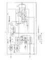
以下、第1実施形態について説明する。本実施形態の通信用スレーブは、特許文献1に開示されているマイクロコンピュータ41に通信機能等を追加したもので構成されている。図7は、特許文献1の図7相当図である。マイコン(マイクロコンピュータシステム)41は、CPU2A,内蔵メモリ3,暴走検知部42などから構成されており、これらは、アドレスバス5,データバス6を介して互いに接続されている。
(First embodiment)
The first embodiment will be described below. The communication slave of this embodiment is configured by adding a communication function and the like to the
CPU2Aは、制御部(信号出力部)7,デコード部8,演算部9,レジスタ部10などを内蔵しており、制御部7は、R/W(リード/ライト)などの制御信号を出力してバス5及び6に対するアクセスを行い、CPU外部とのデータ転送を制御する。内蔵メモリ3にはCPU2Aの制御プログラムが記憶されており、CPU2Aが前記プログラムの命令や、内蔵メモリ3に記憶されているデータを読み込むとそれらはレジスタ部10に格納され、デコード部8によりデコードされる。すると、演算部9がその読み込み結果に基づいて演算処理を実行し、演算結果のデータは、必要に応じてレジスタ部10内のデータレジスタ18や内蔵メモリ3に書き込まれる。
The
制御部7は、CPU2Aが実行しているアクセスサイクルが「命令フェッチ」であるか、それ以外の「データアクセス」等であるのかを示す命令フェッチ信号を出力する。また制御部7は、自身が現在実行中であるタスクが、2つのうち何れかを示すタスク情報信号(タスク実行信号)も出力する。各タスクのプログラムは、内蔵メモリ3に記憶されている。
The
2つのタスクの一方は、マイコン1におけるシステムの基層的な部分を管理するため、重要度がより高いタスク(最重要タスク,以下、タスクSと称す)として設定されている。即ち、他方のタスク(以下、タスクXと称す)の暴走を監視するためのルーチンや、フェイルセーフ用のバックアップシーケンスなどを実行する。そして、タスクSは、固定ループ動作することでソフトウエアタイマとしても機能するため、分岐命令などのコーディングは予め禁止されており、基本的にループ周回周期毎に実行が必要な処理を行う。
また、他方のタスクXは、数値演算処理などを行なうのに適したタスクであり、分岐命令の実行も許可されている。そして、タスクXは、タスクSのループ周回回数によって計時される時間を利用した処理も行なう。
One of the two tasks is set as a task having a higher importance (the most important task, hereinafter referred to as task S) in order to manage the basic layer of the system in the
The other task X is a task suitable for performing numerical operation processing and the like, and execution of branch instructions is permitted. Task X also performs processing using the time counted by the number of loops of task S.
暴走検知部42は、タスクS領域(2)上限レジスタ11A,タスクS領域(2)下限レジスタ12A,プログラム領域判定部13,3入力ANDゲート15及び46,タスクS領域(1)上限レジスタ43,タスクS領域(1)下限レジスタ44及びデータ領域判定部45などを備えている。上限レジスタ11A,下限レジスタ12Aには、CPU2Aが起動した場合の初期処理で、内蔵メモリ3におけるタスクSのプログラムアドレスの上限値(終了アドレス),下限値(開始アドレス)が夫々書き込まれる。また、上限レジスタ43には、データ領域の上限値が設定され、下限レジスタ44には、データ領域の下限値が設定される。
The
プログラム領域判定部13は、アドレスバス5に出力されるアドレスと、上記レジスタ12,13に設定保持されるアドレスとを比較して、前者のアドレスがタスクSのプログラム領域内(上限,下限の間)であるか否かを判定する。そして、タスクSのプログラム領域内であれば、その状態を示す領域判定信号をアクティブ(ハイ)にする。領域判定信号は、NOTゲート16を介してANDゲート15の入力端子に与えられている。また、CPU2Aの制御部7が出力するタスク情報信号が、ANDゲート15の入力端子に与えられている。
The program
ANDゲート15の残る1つの入力端子には、制御部7により出力される命令フェッチ信号が与えられている。命令フェッチ信号は、CPU2Aが命令リードサイクルを実行する場合にハイレベルを示す。ANDゲート15,46の出力端子は、具体的には図示しないが、CPU2Aに対し例外処理を実行させるための割り込み信号として出力される。
The remaining one input terminal of the
データ領域判定部45は、プログラム領域判定部13と同様に、アドレスバス3に出力されるアドレスと、上記レジスタ43,44に設定保持されるアドレスとを比較して、前者のアドレスがタスクSのデータ領域内(上限,下限の間)であるか否かを判定する。そして、タスクSのデータ領域内である場合は、その状態を示す領域判定信号をアクティブ(ハイ)にする。領域判定信号は、ANDゲート46の入力端子に与えられている。
Similar to the program
ANDゲート46の他の入力端子の1つには、CPU2の制御部7によって出力される制御信号R/W(リード/ライト)が与えられており、残る1つの入力端子には、タスク情報信号がNOTゲート47を介して与えられている。制御信号R/Wは、CPU2がリードサイクルを実行する場合にロウレベルを、ライトサイクルを実行する場合にハイレベルを示すように出力される。
One of the other input terminals of the
また、ANDゲート15,46の出力端子は、ORゲート48の各入力端子に夫々接続されており、ORゲート48の出力端子は、レジスタ11A,12A,43,44のクリア端子に接続されており、ANDゲート15,46の何れの出力レベルがハイになると、各レジスタはクリアされるようになっている。但し、レジスタ11A,43についてはデータ値が変化しないため、クリア端子を削除しても良い。
The output terminals of the
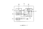
図1に示すように、通信用スレーブ21は、図5に示すマイコン41を用いて構成されている。バス5及び6には通信回路22が接続されている。通信回路22は、通信端子23に通信バスが接続され、マスタ(何れも図示せず)と通信を行う機能を有する。発振回路24は、例えばCR発振回路等で構成されており、CPU2Aを含む通信用スレーブ21の各部にメインクロックを供給する。
As shown in FIG. 1, the
図2に示すように、通信回路22は、受信検出回路25,送信待ち制御回路26,送信回路27,周期検出回路28,バスI/F29等を備えて構成されている。受信検出回路25は、受信端子23Rを介してマスタより送信された信号を受信し、その信号が同期信号である場合のみ出力端子のレベルをハイに変化させて同期検出信号をアクティブにするが、その他の場合はローに維持する。
As shown in FIG. 2, the
送信待ち制御回路26は、加算器30,マルチプレクサ31及び通信カウンタレジスタ32で構成されるサイクルカウンタ33(計測カウンタ,待機時間カウンタ)を備えている。加算器30は、通信カウンタレジスタ32の出力データに「1」を加算した値を、マルチプレクサ31の入力端子の一方に出力する。マルチプレクサ31の入力端子の他方にはデータ値「0」が与えられている。マルチプレクサ31の切り換え制御は同期検出信号によって行われ、当該信号がローであれば加算器30側を選択し、ハイであればデータ値「0」側を選択する。
The transmission
通信カウンタレジスタ32は、発振回路24より供給されるメインクロックパルスが入力される毎にレジスタ値を更新する。したがって、同期検出信号がローレベルを示す期間は通信カウンタレジスタ32の値はメインクロックパルスが入力される毎にインクリメントされ続け、同期検出信号がハイレベルを示すとゼロクリアされる。尚、メインクロックは、以降に説明する「レジスタ」の全てに供給されており、各レジスタは、メインクロックパルスの入力タイミングでレジスタ値を更新する。
The
比較器34は、通信カウンタレジスタ32のレジスタ値と、送信待ち時間レジスタ35のレジスタ値とを比較する。送信待ち時間レジスタ35には、バスI/F29を介してCPU2Aより送信待ち時間相当値が書き込み設定される。そして、比較器34は、双方のレジスタ値が一致すると、送信回路27に送信要求トリガを出力する。上記メインクロックパルスは、送信回路27にも入力されている。
The
同期検出信号は、周期検出回路28のANDゲート36(禁止手段)の一方の入力端子に与えられている。また、ANDゲート36の他方の入力端子には、モニタ許可レジスタ37(禁止手段)のレジスタ値が与えられている。モニタ許可レジスタ37は、送信待ち時間レジスタ35と同様に、バスI/F29を介してCPU2Aより、許可/禁止に応じて1/0のデータ値が書き込み設定される。ANDゲート36の出力信号は、マルチプレクサ38,39の切り換えを制御する。
The synchronization detection signal is given to one input terminal of the AND gate 36 (prohibiting means) of the
マルチプレクサ38の出力端子は、モニタ用サイクル数レジスタ50の入力端子に接続されており、マルチプレクサ38の入力端子の一方は、モニタ用サイクル数レジスタ50の出力端子に接続されている。また、マルチプレクサ38の入力端子の一方には、通信カウンタレジスタ32のレジスタ値が与えられている。マルチプレクサ38は、ANDゲート36の出力信号がハイレベルであれば通信カウンタレジスタ32側を選択し、ローレベルであればモニタ用サイクル数レジスタ50側を選択する。
The output terminal of the
したがって、モニタ用サイクル数レジスタ50のレジスタ値は、上記信号がハイレベルであれば通信カウンタレジスタ32のレジスタ値で更新され、ローレベルであればその時点のレジスタ値を維持する。そして、モニタ用サイクル数レジスタ50のレジスタ値は、バスI/F29を介してデータバス6に出力可能となっている。
Therefore, the register value of the monitor
マルチプレクサ39(フラグセット部)の出力端子は、もう1つのマルチプレクサ51(フラグセット部)を介して検出フラグレジスタ52(フラグセット部)の入力端子に接続されている。マルチプレクサ39の入力端子の一方は、検出フラグレジスタ52の出力端子に接続されており、入力端子の他方にはデータ値「1」が与えられている。また、マルチプレクサ51の入力端子の他方にはデータ値「0」が与えられている。マルチプレクサ51の切り換え制御は「ソフトクリア要求」によって行われる。
The output terminal of the multiplexer 39 (flag set unit) is connected to the input terminal of the detection flag register 52 (flag set unit) via another multiplexer 51 (flag set unit). One of the input terminals of the
ここで「ソフトクリア要求」とは、CPU2Aのプログラム動作により検出フラグレジスタ52をクリアすることを意味し、例えば図示しないクリア要のレジスタにCPU2Aが書き込みを行うことで、所定期間だけデータ値「1」が出力されてマルチプレクサ51を切り替える。
Here, the “soft clear request” means that the
したがって、検出フラグレジスタ52のレジスタ値は、ソフトクリア要求が発生しない限りその時点のレジスタ値を維持し、ソフトクリア要求が発生するとゼロクリアされる。そして、検出フラグレジスタ52のレジスタ値は、ANDゲート36の出力信号がハイレベルになるとマルチプレクサ39及び51を介してデータ値「1」が格納される。この検出フラグレジスタ52のレジスタ値も、バスI/F29を介してデータバス6に出力可能となっている。
Therefore, the register value of the
次に、本実施形態の作用について図3及び図4を参照して説明する。尚、暴走検知部42によるCPU2Aの暴走検知処理については特許文献1と同様であるから、説明を省略する。図4に示すように、マスタは周期的に(例えば数100μs程度)、通信バス上に同期信号を出力する。そして、各スレーブ(1〜3)は、同期信号をトリガとして各スレーブに設定される待機時間(待ち(1)〜(3))の経過待ちをした後に、マスタに対してデータを送信する。
Next, the effect | action of this embodiment is demonstrated with reference to FIG.3 and FIG.4. Note that the runaway detection processing of the
マスタに搭載される発振回路は例えば水晶発振子を用いたもので、同期信号の出力周期は高精度のクロック信号に基づいて決定されている。一方、スレーブについては、一般に1つの通信ネットワークに数多く接続されるノードであるため、コストの制約から高価な水晶発振子を用いることはなく、安価なCR発振回路等が用いられている。そこで、本実施形態の通信用スレーブ21は、図3に示すように、同期信号の出力間隔を、発振回路24が出力するメインクロックを用いてカウントする((a)〜(c)参照)。そして、そのカウント値をモニタすることで、発振回路24の発振動作が正常か否かを監視する。
The oscillation circuit mounted on the master uses a crystal oscillator, for example, and the output period of the synchronization signal is determined based on a highly accurate clock signal. On the other hand, since the slave is a node generally connected to one communication network, an expensive crystal oscillator is used without using an expensive crystal oscillator due to cost restrictions. Therefore, as shown in FIG. 3, the
尚、通信バス上に、同期信号以外の通信用データも伝送される場合は、受信検出回路25において両者を弁別すれば良い。また、例えばDSI等のプロトコルでは、マスタが送信するデータはバス上の電圧を変化させ、スレーブが送信するデータはバス上の電流を変化させて伝送するので、受信検出回路25では電圧の変化を捉えるようにすれば同期信号を検出できる。
When communication data other than the synchronization signal is also transmitted on the communication bus, the
図5に示す初期設定処理では、先ず自身のスレーブIDを取得するが(S1)、その取得方法については特に限定しない。例えば、マスタより送信されるコマンドより取得しても良い。それから、送信待ち時間指示レジスタ35に送信待ち時間を書き込んで設定する(S2)。送信待ち時間は、各スレーブ毎に異なる時間を設定するが(図4参照)、例えば上記スレーブIDの値に基づいて設定しても良い。そして、モニタ許可レジスタ37にデータ「1」を書き込んで、同期信号の間隔検出(モニタ)を許可すると(S3)処理を終了する。 In the initial setting process shown in FIG. 5, the slave ID is first acquired (S1), but the acquisition method is not particularly limited. For example, it may be acquired from a command transmitted from the master. Then, the transmission waiting time is written and set in the transmission waiting time instruction register 35 (S2). The transmission waiting time is set differently for each slave (see FIG. 4), but may be set based on the value of the slave ID, for example. Then, when data “1” is written in the monitor permission register 37 and the interval detection (monitoring) of the synchronization signal is permitted (S3), the process is terminated.
図6に示す発振異常監視処理は、複数のタスクの何れか1つ(発振異常監視タスク)により実行される。この処理は、例えば最重要タスクが行うようにしても良い。先ず、検出フラグレジスタ52を参照して、検出フラグがセットされているか否かを判断する(S11)。図3(e)に示すように、検出フラグがセットされていれば(YES)、モニタ用サイクル数レジスタ50のレジスタ値を読み出す(S12)。そして、前記レジスタ値が正常範囲内か否かを判断する(S13)。
The oscillation abnormality monitoring process shown in FIG. 6 is executed by any one of a plurality of tasks (oscillation abnormality monitoring task). This processing may be performed by the most important task, for example. First, it is determined whether or not the detection flag is set with reference to the detection flag register 52 (S11). As shown in FIG. 3E, if the detection flag is set (YES), the register value of the monitor
ここで、「正常範囲」とは、例えばシステム仕様で定められている同期信号の出力周期に相当するメインクロックによるカウント値に、所定の許容値αを加減したものに設定する。モニタ用サイクル数レジスタ50の値が正常範囲内であれば(YES)、異常検知カウンタをクリアする(S14)。「異常検知カウンタ」は、発振異常監視処理内のソフトウェアカウンタである。それから、検出フラグをクリアすると(S15)処理を終了する。
Here, the “normal range” is set to, for example, a value obtained by adding or subtracting a predetermined allowable value α to the count value by the main clock corresponding to the output period of the synchronization signal defined in the system specifications. If the value of the monitor
一方、ステップS13においてモニタ用サイクル数レジスタ50の値が正常範囲外であれば(NO)異常検知カウンタをインクリメントして(S16)、当該カウンタの値が所定値(例えば「3」)に達したか否かを判断する(S17)。所定値に達していなければ(NO)ステップS15に移行し、所定値に達していれば(YES)異常検知処理を行う(S18)。例えば、表示器等の報知手段により発振回路24が異常であることを報知する。ステップS13において「NO」と判断するのは、図3(b),(c)に示すように、周波数が正常範囲を超えて上昇した場合と、正常範囲を下回るように低下した場合とになる。
On the other hand, if the value of the monitor
以上のように本実施形態によれば、通信用スレーブ21を構成するCPU2Aの制御部7は、CPU2AがタスクSを実行している期間にタスク情報信号をアクティブにする。暴走検知部42のプログラム領域判定部13は、タスクSのプログラムが格納されている内蔵メモリ3の上限アドレス,下限アドレスが設定されているレジスタ11,12のレジスタ値とCPU2Aが実行中のプログラムアドレスとを比較して、後者がタスクSの実行領域を示すか否かを判定する。また、データ領域判定部45は、最重要タスクSのデータが格納されているメモリ領域の開始アドレス,終了アドレスが設定されているレジスタ値とCPU2Aが実行中のアドレスとを比較して、最重要タスクSのデータ領域であるか否かを判定する。
As described above, according to the present embodiment, the
そして、暴走検知部42は、プログラム領域判定部13による判定結果とタスク実行信号の出力状態とが不一致である場合に、又はデータ領域判定部45による判定結果とタスク実行信号の出力状態とが不一致である場合に暴走を検知する。従って、最重要タスクSのプログラム領域,データ領域に対して不正なアクセスが行われた場合に、ロジック回路により迅速に暴走を検知できる。
The
そして、通信回路22では、サイクルカウンタ33により、マスタが周期的に送信する同期信号の受信間隔を、発振回路24が出力するメインクロックに基づくカウント動作により計測し、発振異常監視タスクは、モニタ用サイクル数レジスタ50に格納されているサイクルカウンタ33の計測値を読み出して、当該計測値が正常範囲を超えると発振回路24の異常を検知する。したがって、マスタとの間で非同期式通信を行う通信用スレーブ21においても、同期信号の受信間隔を発振回路24が出力するメインクロックに基づき計測することで、発振回路24の異常を検知できる。
In the
また、サイクルカウンタ33には、同期信号を受信してからマスタとの通信を開始するまでの待機時間を計時するための待機時間カウンタを利用するので、新規な回路部品要素の追加を抑制できる。また、同期信号を受信すると検出フラグがセットされる検出フラグレジスタ52を備え、発振異常監視タスクは、検出フラグがセットされるとモニタ用サイクル数レジスタ50格納された計測値を読み出すので、レジスタ50への不要なアクセスを抑制できる。
In addition, since the
更に、モニタ許可レジスタ37に書き込みを行うことで同期信号の受信伝達経路を遮断して、発振異常監視タスクによる発振回路24の異常検知処理を禁止可能としたので、必要に応じて発振回路24の異常検知を行うことができる。加えて、発振異常監視タスクは、計測値が正常範囲を超えると異常検知カウンタをインクリメントし、計測値が正常範囲内であれば異常検知カウンタをクリアして、異常検知カウンタの値が所定値に達すると発振回路24の異常を検知する。したがって、発振回路24の異常を確実に検知することができる。
Furthermore, by writing to the
(第2実施形態)
以下、第1実施形態と同一部分には同一符号を付して説明を省略し、異なる部分について説明する。図8に示すように、第2実施形態は、図6に示すフローチャートのステップS14をS14’に置き換えたもので、モニタ用サイクル数レジスタ50のレジスタ値が正常範囲内であれば、異常検知カウンタをデクリメントする(尚、カウンタ値が「0」であれば「0」を維持する)。異常検知カウンタは、正常範囲外であればステップS16でインクリメントされるので、そのように増減を行った結果としてカウンタ値が所定値に達すれば、ステップS18で異常検知処理が行われる。この様な第2実施形態による場合も、第1実施形態と同様の効果が得られる。
(Second Embodiment)
Hereinafter, the same parts as those in the first embodiment are denoted by the same reference numerals, description thereof will be omitted, and different parts will be described. As shown in FIG. 8, in the second embodiment, step S14 in the flowchart shown in FIG. 6 is replaced with S14 ′, and if the register value of the monitor
(第3実施形態)
図9に示すように、第3実施形態は、図5に示す初期設定処理にステップS4,S5を追加したものである。すなわち、初期設定処理の最初はコマンドモードとなり、マスタより周期設定コマンドが送信される(S4)。周期設定コマンドには、同期信号の出力周期を示すデータが含まれている。各スレーブは上記コマンドを受信して周期データを取得すると、それに許容範囲を加減することで判定用の「正常範囲」を設定する(S5)。
(Third embodiment)
As shown in FIG. 9, the third embodiment is obtained by adding steps S4 and S5 to the initial setting process shown in FIG. That is, at the beginning of the initial setting process, the command mode is set, and a cycle setting command is transmitted from the master (S4). The cycle setting command includes data indicating the output cycle of the synchronization signal. When each slave receives the command and acquires the period data, it sets a “normal range” for determination by adding or subtracting an allowable range to the slave data (S5).
以上のように第3実施形態によれば、発振異常監視タスクは、マスタにより送信される周期設定コマンドを受信すると、そのコマンドに含まれている出力周期データに基づいて正常範囲を設定するので、同期信号の出力間隔がダイナミックに変更設定されるシステム仕様についても対応することができる。 As described above, according to the third embodiment, when the oscillation abnormality monitoring task receives the cycle setting command transmitted from the master, the normal range is set based on the output cycle data included in the command. It is also possible to cope with system specifications in which the output interval of the synchronization signal is dynamically changed.
(第4実施形態)
第4実施形態は、図10に示す正常範囲設定処理を実行する。すなわち、最初に検出フラグがセットされて(S21:YES)、モニタ用サイクル数レジスタ50のレジスタ値を取得すると(S22)、そのレジスタ値(初期サイクル数)に基づいて正常範囲を設定する(S23)。すなわち、実際の同期信号の出力間隔を最初に計測した値に基づいて正常範囲を設定する。このような第4実施形態による場合も、第3実施形態と同様の効果が得られる。
(Fourth embodiment)
In the fourth embodiment, the normal range setting process shown in FIG. 10 is executed. That is, when the detection flag is first set (S21: YES) and the register value of the monitoring
本発明は上記した、又は図面に記載した実施例にのみ限定されるものではなく、以下のような変形又は拡張が可能である。
同期信号の出力周期については、個別の設計に応じて適宜設定すれば良い。
検出フラグがセットされるとCPU2Aに割り込みを発生させて、その割り込みにより発振異常監視処理を行うようにしても良い。
計測カウンタと待機時間カウンタとを別個に設けても良い。
ANDゲート36及びモニタ許可レジスタ37は、必要に応じて設ければ良い。
マスタとスレーブとの通信は、1対1で行っても良い。
The present invention is not limited to the embodiments described above or shown in the drawings, and the following modifications or expansions are possible.
What is necessary is just to set suitably the output period of a synchronizing signal according to an individual design.
When the detection flag is set, an interrupt may be generated in the
A measurement counter and a standby time counter may be provided separately.
The AND
Communication between the master and the slave may be performed on a one-to-one basis.
図面中、2AはCPU、3は内蔵メモリ、4は暴走検知部、7は制御部(信号出力部)、11はタスクS領域上限レジスタ、12はタスクS領域下限レジスタ、13はプログラム領域判定部、21は通信用スレーブ、24は発振回路、33はサイクルカウンタ(計測カウンタ,待機時間カウンタ)、41はマイクロコンピュータ(マイクロコンピュータシステム)、45はデータ領域判定部、50はモニタ用サイクル数レジスタ、52は検出フラグレジスタ(フラグセット部)を示す。
In the drawing, 2A is a CPU, 3 is a built-in memory, 4 is a runaway detection unit, 7 is a control unit (signal output unit), 11 is a task S area upper limit register, 12 is a task S area lower limit register, and 13 is a program area determination unit. , 21 is a communication slave, 24 is an oscillation circuit, 33 is a cycle counter (measurement counter, standby time counter), 41 is a microcomputer (microcomputer system), 45 is a data area determination unit, 50 is a monitor cycle number register,
Claims (8)
システム上の重要度が最高に設定されていると共に、実行間隔が一定となる最重要タスクを含む、複数のタスクを時分割並行的に実施可能であるCPU(2A)と、
このCPUが前記最重要タスクを実行している期間に、タスク実行信号を出力する信号出力部(7)と、
前記最重要タスクのプログラムが格納されているメモリ領域(3)の開始アドレス,終了アドレスの設定値と、前記CPUが実行中のアドレスとを比較することで、前記最重要タスクのプログラム領域であるか否かを判定するプログラム領域判定部(13)と、
前記最重要タスクのデータが格納されているメモリ領域の開始アドレス,終了アドレス
の設定値と、前記CPUが実行中のアドレスとを比較することで、前記最重要タスクのデータ領域であるか否かを判定するデータ領域判定部(45)と、
前記プログラム領域判定部による判定結果と前記タスク実行信号の出力状態とを参照して、双方が不一致である場合に暴走を検知し、また、前記データ領域判定部による判定結果と前記タスク実行信号の出力状態とを参照して、双方が不一致である場合に暴走を検知する暴走検知部(42)と、
前記CPUにクロック信号を供給する発振回路(24)と、
前記マスタが周期的に送信する同期信号の受信間隔を、前記クロック信号に基づくカウント動作により計測する計測カウンタ(33)と、
前記同期信号を受信したタイミングで、前記計測カウンタの計測値が格納されるモニタ用レジスタ(50)とを備え、
前記複数のタスクの何れか1つ(発振異常監視タスクと称す)は、前記モニタ用レジスタに格納された計測値を読み出して、当該計測値が正常範囲を超えると、前記発振回路の異常を検知することを特徴とする通信用スレーブ。 A communication slave (21) for performing asynchronous communication with a master connected via a communication bus,
A CPU (2A) capable of performing a plurality of tasks in a time-sharing manner in parallel, including the most important task having the highest importance on the system and a constant execution interval;
A signal output unit (7) for outputting a task execution signal during a period in which the CPU executes the most important task;
It is the program area of the most important task by comparing the set values of the start address and end address of the memory area (3) in which the program of the most important task is stored with the address being executed by the CPU. A program area determination unit (13) for determining whether or not
Whether or not it is the data area of the most important task by comparing the set values of the start address and end address of the memory area in which the data of the most important task is stored with the address being executed by the CPU A data area determination unit (45) for determining
With reference to the determination result by the program area determination unit and the output state of the task execution signal, a runaway is detected when both do not match, and the determination result by the data area determination unit and the task execution signal With reference to the output state, a runaway detection unit (42) that detects a runaway when both do not match,
An oscillation circuit (24) for supplying a clock signal to the CPU;
A measurement counter (33) for measuring a reception interval of the synchronization signal periodically transmitted by the master by a counting operation based on the clock signal;
Wherein at a timing of receiving the synchronization signal, and a monitor register (50) the measured value of the thermometer Hakaka counter is stored,
Wherein one of the plurality of tasks (called oscillation abnormality monitoring task) reads the metrology value stored in the monitor register, exceeds the measurement value is positive normal range, an abnormality of the oscillator circuit A slave for communication characterized by detection.
前記計測カウンタに、前記待機時間カウンタを使用することを特徴とする請求項1記載の通信用スレーブ。 A standby time counter for measuring a standby time from the reception of the synchronization signal to the start of communication with the master;
The communication slave according to claim 1, wherein the waiting time counter is used as the measurement counter.
前記発振異常監視タスクは、前記検出フラグがセットされると、前記モニタ用レジスタに格納された計測値を読み出すことを特徴とする請求項1又は2記載の通信用スレーブ。 A flag setting unit (39, 51, 52) in which a detection flag is set when the synchronization signal is received;
3. The communication slave according to claim 1, wherein the oscillation abnormality monitoring task reads a measurement value stored in the monitor register when the detection flag is set.
前記計測値が前記正常範囲内であれば、前記異常検知カウンタをクリアして、
前記異常検知カウンタのカウンタ値が所定値に達すると、前記発振回路の異常を検知することを特徴とする請求項1から4の何れか一項に記載の通信用スレーブ。 The oscillation abnormality monitoring task increments an abnormality detection counter when the measured value exceeds the normal range,
If the measured value is within the normal range, clear the abnormality detection counter,
The communication slave according to any one of claims 1 to 4, wherein when the counter value of the abnormality detection counter reaches a predetermined value, an abnormality of the oscillation circuit is detected.
前記計測値が前記正常範囲内であれば、前記異常検知カウンタをデクリメントして、
前記異常検知カウンタのカウンタ値が所定値に達すると、前記発振回路の異常を検知することを特徴とする請求項1から4の何れか一項に記載の通信用スレーブ。 The oscillation abnormality monitoring task increments an abnormality detection counter when the measured value exceeds the normal range,
If the measured value is within the normal range, decrement the abnormality detection counter,
The communication slave according to any one of claims 1 to 4, wherein when the counter value of the abnormality detection counter reaches a predetermined value, an abnormality of the oscillation circuit is detected.
Priority Applications (1)
| Application Number | Priority Date | Filing Date | Title |
|---|---|---|---|
| JP2013029034A JP5987723B2 (en) | 2013-02-18 | 2013-02-18 | Slave for communication |
Applications Claiming Priority (1)
| Application Number | Priority Date | Filing Date | Title |
|---|---|---|---|
| JP2013029034A JP5987723B2 (en) | 2013-02-18 | 2013-02-18 | Slave for communication |
Publications (2)
| Publication Number | Publication Date |
|---|---|
| JP2014157554A JP2014157554A (en) | 2014-08-28 |
| JP5987723B2 true JP5987723B2 (en) | 2016-09-07 |
Family
ID=51578373
Family Applications (1)
| Application Number | Title | Priority Date | Filing Date |
|---|---|---|---|
| JP2013029034A Active JP5987723B2 (en) | 2013-02-18 | 2013-02-18 | Slave for communication |
Country Status (1)
| Country | Link |
|---|---|
| JP (1) | JP5987723B2 (en) |
Families Citing this family (2)
| Publication number | Priority date | Publication date | Assignee | Title |
|---|---|---|---|---|
| DE102017217723A1 (en) * | 2017-10-05 | 2019-04-11 | Robert Bosch Gmbh | Apparatus and method for correcting at least one transmission parameter |
| JP2020086934A (en) * | 2018-11-26 | 2020-06-04 | 株式会社村田製作所 | Counter read circuit |
Family Cites Families (5)
| Publication number | Priority date | Publication date | Assignee | Title |
|---|---|---|---|---|
| JPH10247121A (en) * | 1997-03-05 | 1998-09-14 | Sanyo Electric Co Ltd | Microcomputer |
| JP3991782B2 (en) * | 2002-06-24 | 2007-10-17 | 株式会社デンソー | Electronic control unit |
| JP4893427B2 (en) * | 2006-06-30 | 2012-03-07 | 株式会社デンソー | Microcomputer system |
| JP2009017130A (en) * | 2007-07-03 | 2009-01-22 | Sanyo Electric Co Ltd | Electronic circuit equipped with two or more oscillation circuits |
| JP5509055B2 (en) * | 2009-12-24 | 2014-06-04 | キヤノンファインテック株式会社 | Image forming apparatus |
-
2013
- 2013-02-18 JP JP2013029034A patent/JP5987723B2/en active Active
Also Published As
| Publication number | Publication date |
|---|---|
| JP2014157554A (en) | 2014-08-28 |
Similar Documents
| Publication | Publication Date | Title |
|---|---|---|
| KR101283431B1 (en) | Microcomputer | |
| WO2016062084A1 (en) | Power-off processing method and apparatus, and electronic device | |
| JP6054010B2 (en) | Data determination apparatus, data determination method, and program | |
| US9841795B2 (en) | Method for resetting an electronic device having independent device domains | |
| US20180089046A1 (en) | Self-diagnosis device and self-diagnosis method | |
| JP5987723B2 (en) | Slave for communication | |
| JP5545250B2 (en) | Control device | |
| JP5434942B2 (en) | Control device | |
| JP6049961B1 (en) | CPU monitoring device | |
| JP2010009258A (en) | Fault detection device of software | |
| JP6187508B2 (en) | Control device, bus circuit, method, and program | |
| JP4322606B2 (en) | Watchdog timer | |
| JP2011154459A (en) | Program abnormal operation detection device for computer system | |
| US8527743B2 (en) | Simultaneous checking of plural exit conditions loaded in table subsequent to execution of wait instruction for jitter free exit | |
| JP6741940B2 (en) | Information processing device and PLD management program | |
| JP4842036B2 (en) | Semiconductor device and abnormality detection method of timing control circuit | |
| US10719117B2 (en) | Control apparatus configured to control clock signal generation, method for controlling the same, storage medium, and computer system | |
| JPH0581138A (en) | Microprogram controller | |
| JP3977694B2 (en) | Reset device | |
| JP2014002649A (en) | Semiconductor device and access timing adjustment method | |
| JP6161105B2 (en) | Information processing system | |
| JP4063699B2 (en) | Program runaway detection circuit | |
| JP2001256059A (en) | Interruption input unit and plc system | |
| JP2011191830A (en) | Memory diagnostic method and control equipment for power converter | |
| JP2018025983A (en) | Semiconductor device and control method of the same |
Legal Events
| Date | Code | Title | Description |
|---|---|---|---|
| A621 | Written request for application examination |
Free format text: JAPANESE INTERMEDIATE CODE: A621 Effective date: 20150417 |
|
| A977 | Report on retrieval |
Free format text: JAPANESE INTERMEDIATE CODE: A971007 Effective date: 20151228 |
|
| A131 | Notification of reasons for refusal |
Free format text: JAPANESE INTERMEDIATE CODE: A131 Effective date: 20160112 |
|
| A521 | Request for written amendment filed |
Free format text: JAPANESE INTERMEDIATE CODE: A523 Effective date: 20160223 |
|
| TRDD | Decision of grant or rejection written | ||
| A01 | Written decision to grant a patent or to grant a registration (utility model) |
Free format text: JAPANESE INTERMEDIATE CODE: A01 Effective date: 20160712 |
|
| A61 | First payment of annual fees (during grant procedure) |
Free format text: JAPANESE INTERMEDIATE CODE: A61 Effective date: 20160725 |
|
| R151 | Written notification of patent or utility model registration |
Ref document number: 5987723 Country of ref document: JP Free format text: JAPANESE INTERMEDIATE CODE: R151 |
|
| R250 | Receipt of annual fees |
Free format text: JAPANESE INTERMEDIATE CODE: R250 |
|
| R250 | Receipt of annual fees |
Free format text: JAPANESE INTERMEDIATE CODE: R250 |
|
| R250 | Receipt of annual fees |
Free format text: JAPANESE INTERMEDIATE CODE: R250 |
|
| R250 | Receipt of annual fees |
Free format text: JAPANESE INTERMEDIATE CODE: R250 |
|
| R250 | Receipt of annual fees |
Free format text: JAPANESE INTERMEDIATE CODE: R250 |