JP5974429B2 - Composite material structure and manufacturing method thereof - Google Patents
Composite material structure and manufacturing method thereof Download PDFInfo
- Publication number
- JP5974429B2 JP5974429B2 JP2011158723A JP2011158723A JP5974429B2 JP 5974429 B2 JP5974429 B2 JP 5974429B2 JP 2011158723 A JP2011158723 A JP 2011158723A JP 2011158723 A JP2011158723 A JP 2011158723A JP 5974429 B2 JP5974429 B2 JP 5974429B2
- Authority
- JP
- Japan
- Prior art keywords
- space
- flow path
- base material
- liquid
- microchip
- Prior art date
- Legal status (The legal status is an assumption and is not a legal conclusion. Google has not performed a legal analysis and makes no representation as to the accuracy of the status listed.)
- Active
Links
- 238000004519 manufacturing process Methods 0.000 title claims description 21
- 239000002131 composite material Substances 0.000 title description 36
- 239000000463 material Substances 0.000 claims description 106
- 239000007788 liquid Substances 0.000 claims description 42
- 229920005992 thermoplastic resin Polymers 0.000 claims description 28
- 239000011859 microparticle Substances 0.000 claims description 22
- 238000000034 method Methods 0.000 claims description 18
- 239000000758 substrate Substances 0.000 claims description 8
- 230000001678 irradiating effect Effects 0.000 claims description 5
- 238000005304 joining Methods 0.000 claims description 3
- 238000002834 transmittance Methods 0.000 claims description 3
- 238000005516 engineering process Methods 0.000 description 17
- 230000003287 optical effect Effects 0.000 description 17
- 238000004458 analytical method Methods 0.000 description 12
- 238000001514 detection method Methods 0.000 description 11
- 239000010419 fine particle Substances 0.000 description 9
- 238000010586 diagram Methods 0.000 description 7
- VYPSYNLAJGMNEJ-UHFFFAOYSA-N silicon dioxide Inorganic materials O=[Si]=O VYPSYNLAJGMNEJ-UHFFFAOYSA-N 0.000 description 7
- 210000004027 cell Anatomy 0.000 description 5
- 238000005259 measurement Methods 0.000 description 5
- 239000010453 quartz Substances 0.000 description 5
- 239000011521 glass Substances 0.000 description 4
- 229910052751 metal Inorganic materials 0.000 description 4
- 239000002184 metal Substances 0.000 description 4
- 239000002245 particle Substances 0.000 description 4
- 239000004743 Polypropylene Substances 0.000 description 3
- 230000005540 biological transmission Effects 0.000 description 3
- 230000008602 contraction Effects 0.000 description 3
- 238000003754 machining Methods 0.000 description 3
- 229920003229 poly(methyl methacrylate) Polymers 0.000 description 3
- 239000002861 polymer material Substances 0.000 description 3
- 239000004926 polymethyl methacrylate Substances 0.000 description 3
- 239000004793 Polystyrene Substances 0.000 description 2
- 238000004891 communication Methods 0.000 description 2
- 238000001746 injection moulding Methods 0.000 description 2
- 229920000592 inorganic polymer Polymers 0.000 description 2
- 239000002502 liposome Substances 0.000 description 2
- 244000005700 microbiome Species 0.000 description 2
- 238000000465 moulding Methods 0.000 description 2
- 210000003463 organelle Anatomy 0.000 description 2
- 229920000620 organic polymer Polymers 0.000 description 2
- -1 polyethylene Polymers 0.000 description 2
- 229920002223 polystyrene Polymers 0.000 description 2
- 229920005989 resin Polymers 0.000 description 2
- 239000011347 resin Substances 0.000 description 2
- 239000003566 sealing material Substances 0.000 description 2
- CHRJZRDFSQHIFI-UHFFFAOYSA-N 1,2-bis(ethenyl)benzene;styrene Chemical compound C=CC1=CC=CC=C1.C=CC1=CC=CC=C1C=C CHRJZRDFSQHIFI-UHFFFAOYSA-N 0.000 description 1
- 241000894006 Bacteria Species 0.000 description 1
- 238000000018 DNA microarray Methods 0.000 description 1
- 241000196324 Embryophyta Species 0.000 description 1
- 241000588724 Escherichia coli Species 0.000 description 1
- 241000233866 Fungi Species 0.000 description 1
- 108091005461 Nucleic proteins Proteins 0.000 description 1
- 239000004698 Polyethylene Substances 0.000 description 1
- 240000004808 Saccharomyces cerevisiae Species 0.000 description 1
- 241000723873 Tobacco mosaic virus Species 0.000 description 1
- 241000700605 Viruses Species 0.000 description 1
- 239000000853 adhesive Substances 0.000 description 1
- 230000001070 adhesive effect Effects 0.000 description 1
- 229910052782 aluminium Inorganic materials 0.000 description 1
- XAGFODPZIPBFFR-UHFFFAOYSA-N aluminium Chemical compound [Al] XAGFODPZIPBFFR-UHFFFAOYSA-N 0.000 description 1
- 210000004102 animal cell Anatomy 0.000 description 1
- 210000000601 blood cell Anatomy 0.000 description 1
- 239000000919 ceramic Substances 0.000 description 1
- 210000000349 chromosome Anatomy 0.000 description 1
- 125000004122 cyclic group Chemical group 0.000 description 1
- 238000013461 design Methods 0.000 description 1
- 238000006073 displacement reaction Methods 0.000 description 1
- 238000001312 dry etching Methods 0.000 description 1
- 229920001971 elastomer Polymers 0.000 description 1
- 239000007863 gel particle Substances 0.000 description 1
- PCHJSUWPFVWCPO-UHFFFAOYSA-N gold Chemical compound [Au] PCHJSUWPFVWCPO-UHFFFAOYSA-N 0.000 description 1
- 238000003384 imaging method Methods 0.000 description 1
- 238000003780 insertion Methods 0.000 description 1
- 230000037431 insertion Effects 0.000 description 1
- 239000004816 latex Substances 0.000 description 1
- 229920000126 latex Polymers 0.000 description 1
- 238000004811 liquid chromatography Methods 0.000 description 1
- 239000000696 magnetic material Substances 0.000 description 1
- 150000002739 metals Chemical class 0.000 description 1
- 239000011325 microbead Substances 0.000 description 1
- 210000003470 mitochondria Anatomy 0.000 description 1
- 239000000203 mixture Substances 0.000 description 1
- 238000012986 modification Methods 0.000 description 1
- 230000004048 modification Effects 0.000 description 1
- 102000039446 nucleic acids Human genes 0.000 description 1
- 108020004707 nucleic acids Proteins 0.000 description 1
- 150000007523 nucleic acids Chemical class 0.000 description 1
- 239000004417 polycarbonate Substances 0.000 description 1
- 229920000515 polycarbonate Polymers 0.000 description 1
- 229920000573 polyethylene Polymers 0.000 description 1
- 229920000642 polymer Polymers 0.000 description 1
- 229920000098 polyolefin Polymers 0.000 description 1
- 229920001155 polypropylene Polymers 0.000 description 1
- 102000004169 proteins and genes Human genes 0.000 description 1
- 230000000717 retained effect Effects 0.000 description 1
- 238000007789 sealing Methods 0.000 description 1
- 239000004065 semiconductor Substances 0.000 description 1
- 238000007493 shaping process Methods 0.000 description 1
- 239000010703 silicon Substances 0.000 description 1
- 229910052710 silicon Inorganic materials 0.000 description 1
- 239000000377 silicon dioxide Substances 0.000 description 1
- 239000000126 substance Substances 0.000 description 1
- 238000001039 wet etching Methods 0.000 description 1
Images


Classifications
-
- B—PERFORMING OPERATIONS; TRANSPORTING
- B32—LAYERED PRODUCTS
- B32B—LAYERED PRODUCTS, i.e. PRODUCTS BUILT-UP OF STRATA OF FLAT OR NON-FLAT, e.g. CELLULAR OR HONEYCOMB, FORM
- B32B3/00—Layered products comprising a layer with external or internal discontinuities or unevennesses, or a layer of non-planar shape; Layered products comprising a layer having particular features of form
- B32B3/26—Layered products comprising a layer with external or internal discontinuities or unevennesses, or a layer of non-planar shape; Layered products comprising a layer having particular features of form characterised by a particular shape of the outline of the cross-section of a continuous layer; characterised by a layer with cavities or internal voids ; characterised by an apertured layer
- B32B3/30—Layered products comprising a layer with external or internal discontinuities or unevennesses, or a layer of non-planar shape; Layered products comprising a layer having particular features of form characterised by a particular shape of the outline of the cross-section of a continuous layer; characterised by a layer with cavities or internal voids ; characterised by an apertured layer characterised by a layer formed with recesses or projections, e.g. hollows, grooves, protuberances, ribs
-
- B—PERFORMING OPERATIONS; TRANSPORTING
- B01—PHYSICAL OR CHEMICAL PROCESSES OR APPARATUS IN GENERAL
- B01L—CHEMICAL OR PHYSICAL LABORATORY APPARATUS FOR GENERAL USE
- B01L3/00—Containers or dishes for laboratory use, e.g. laboratory glassware; Droppers
- B01L3/50—Containers for the purpose of retaining a material to be analysed, e.g. test tubes
- B01L3/502—Containers for the purpose of retaining a material to be analysed, e.g. test tubes with fluid transport, e.g. in multi-compartment structures
- B01L3/5027—Containers for the purpose of retaining a material to be analysed, e.g. test tubes with fluid transport, e.g. in multi-compartment structures by integrated microfluidic structures, i.e. dimensions of channels and chambers are such that surface tension forces are important, e.g. lab-on-a-chip
- B01L3/502707—Containers for the purpose of retaining a material to be analysed, e.g. test tubes with fluid transport, e.g. in multi-compartment structures by integrated microfluidic structures, i.e. dimensions of channels and chambers are such that surface tension forces are important, e.g. lab-on-a-chip characterised by the manufacture of the container or its components
-
- B—PERFORMING OPERATIONS; TRANSPORTING
- B01—PHYSICAL OR CHEMICAL PROCESSES OR APPARATUS IN GENERAL
- B01L—CHEMICAL OR PHYSICAL LABORATORY APPARATUS FOR GENERAL USE
- B01L3/00—Containers or dishes for laboratory use, e.g. laboratory glassware; Droppers
- B01L3/50—Containers for the purpose of retaining a material to be analysed, e.g. test tubes
- B01L3/502—Containers for the purpose of retaining a material to be analysed, e.g. test tubes with fluid transport, e.g. in multi-compartment structures
- B01L3/5027—Containers for the purpose of retaining a material to be analysed, e.g. test tubes with fluid transport, e.g. in multi-compartment structures by integrated microfluidic structures, i.e. dimensions of channels and chambers are such that surface tension forces are important, e.g. lab-on-a-chip
- B01L3/502715—Containers for the purpose of retaining a material to be analysed, e.g. test tubes with fluid transport, e.g. in multi-compartment structures by integrated microfluidic structures, i.e. dimensions of channels and chambers are such that surface tension forces are important, e.g. lab-on-a-chip characterised by interfacing components, e.g. fluidic, electrical, optical or mechanical interfaces
-
- B—PERFORMING OPERATIONS; TRANSPORTING
- B32—LAYERED PRODUCTS
- B32B—LAYERED PRODUCTS, i.e. PRODUCTS BUILT-UP OF STRATA OF FLAT OR NON-FLAT, e.g. CELLULAR OR HONEYCOMB, FORM
- B32B27/00—Layered products comprising a layer of synthetic resin
- B32B27/06—Layered products comprising a layer of synthetic resin as the main or only constituent of a layer, which is next to another layer of the same or of a different material
- B32B27/08—Layered products comprising a layer of synthetic resin as the main or only constituent of a layer, which is next to another layer of the same or of a different material of synthetic resin
-
- B—PERFORMING OPERATIONS; TRANSPORTING
- B32—LAYERED PRODUCTS
- B32B—LAYERED PRODUCTS, i.e. PRODUCTS BUILT-UP OF STRATA OF FLAT OR NON-FLAT, e.g. CELLULAR OR HONEYCOMB, FORM
- B32B3/00—Layered products comprising a layer with external or internal discontinuities or unevennesses, or a layer of non-planar shape; Layered products comprising a layer having particular features of form
- B32B3/02—Layered products comprising a layer with external or internal discontinuities or unevennesses, or a layer of non-planar shape; Layered products comprising a layer having particular features of form characterised by features of form at particular places, e.g. in edge regions
- B32B3/08—Layered products comprising a layer with external or internal discontinuities or unevennesses, or a layer of non-planar shape; Layered products comprising a layer having particular features of form characterised by features of form at particular places, e.g. in edge regions characterised by added members at particular parts
-
- B—PERFORMING OPERATIONS; TRANSPORTING
- B32—LAYERED PRODUCTS
- B32B—LAYERED PRODUCTS, i.e. PRODUCTS BUILT-UP OF STRATA OF FLAT OR NON-FLAT, e.g. CELLULAR OR HONEYCOMB, FORM
- B32B3/00—Layered products comprising a layer with external or internal discontinuities or unevennesses, or a layer of non-planar shape; Layered products comprising a layer having particular features of form
- B32B3/26—Layered products comprising a layer with external or internal discontinuities or unevennesses, or a layer of non-planar shape; Layered products comprising a layer having particular features of form characterised by a particular shape of the outline of the cross-section of a continuous layer; characterised by a layer with cavities or internal voids ; characterised by an apertured layer
- B32B3/266—Layered products comprising a layer with external or internal discontinuities or unevennesses, or a layer of non-planar shape; Layered products comprising a layer having particular features of form characterised by a particular shape of the outline of the cross-section of a continuous layer; characterised by a layer with cavities or internal voids ; characterised by an apertured layer characterised by an apertured layer, the apertures going through the whole thickness of the layer, e.g. expanded metal, perforated layer, slit layer regular cells B32B3/12
-
- G—PHYSICS
- G01—MEASURING; TESTING
- G01N—INVESTIGATING OR ANALYSING MATERIALS BY DETERMINING THEIR CHEMICAL OR PHYSICAL PROPERTIES
- G01N21/00—Investigating or analysing materials by the use of optical means, i.e. using sub-millimetre waves, infrared, visible or ultraviolet light
- G01N21/17—Systems in which incident light is modified in accordance with the properties of the material investigated
- G01N21/47—Scattering, i.e. diffuse reflection
- G01N21/49—Scattering, i.e. diffuse reflection within a body or fluid
- G01N21/51—Scattering, i.e. diffuse reflection within a body or fluid inside a container, e.g. in an ampoule
-
- B—PERFORMING OPERATIONS; TRANSPORTING
- B01—PHYSICAL OR CHEMICAL PROCESSES OR APPARATUS IN GENERAL
- B01L—CHEMICAL OR PHYSICAL LABORATORY APPARATUS FOR GENERAL USE
- B01L2200/00—Solutions for specific problems relating to chemical or physical laboratory apparatus
- B01L2200/06—Fluid handling related problems
- B01L2200/0636—Focussing flows, e.g. to laminate flows
-
- B—PERFORMING OPERATIONS; TRANSPORTING
- B01—PHYSICAL OR CHEMICAL PROCESSES OR APPARATUS IN GENERAL
- B01L—CHEMICAL OR PHYSICAL LABORATORY APPARATUS FOR GENERAL USE
- B01L2200/00—Solutions for specific problems relating to chemical or physical laboratory apparatus
- B01L2200/06—Fluid handling related problems
- B01L2200/0689—Sealing
-
- B—PERFORMING OPERATIONS; TRANSPORTING
- B01—PHYSICAL OR CHEMICAL PROCESSES OR APPARATUS IN GENERAL
- B01L—CHEMICAL OR PHYSICAL LABORATORY APPARATUS FOR GENERAL USE
- B01L2200/00—Solutions for specific problems relating to chemical or physical laboratory apparatus
- B01L2200/12—Specific details about manufacturing devices
-
- B—PERFORMING OPERATIONS; TRANSPORTING
- B01—PHYSICAL OR CHEMICAL PROCESSES OR APPARATUS IN GENERAL
- B01L—CHEMICAL OR PHYSICAL LABORATORY APPARATUS FOR GENERAL USE
- B01L2300/00—Additional constructional details
- B01L2300/06—Auxiliary integrated devices, integrated components
- B01L2300/0627—Sensor or part of a sensor is integrated
- B01L2300/0645—Electrodes
-
- B—PERFORMING OPERATIONS; TRANSPORTING
- B01—PHYSICAL OR CHEMICAL PROCESSES OR APPARATUS IN GENERAL
- B01L—CHEMICAL OR PHYSICAL LABORATORY APPARATUS FOR GENERAL USE
- B01L2300/00—Additional constructional details
- B01L2300/06—Auxiliary integrated devices, integrated components
- B01L2300/0627—Sensor or part of a sensor is integrated
- B01L2300/0654—Lenses; Optical fibres
-
- B—PERFORMING OPERATIONS; TRANSPORTING
- B01—PHYSICAL OR CHEMICAL PROCESSES OR APPARATUS IN GENERAL
- B01L—CHEMICAL OR PHYSICAL LABORATORY APPARATUS FOR GENERAL USE
- B01L2300/00—Additional constructional details
- B01L2300/08—Geometry, shape and general structure
- B01L2300/0809—Geometry, shape and general structure rectangular shaped
- B01L2300/0816—Cards, e.g. flat sample carriers usually with flow in two horizontal directions
-
- B—PERFORMING OPERATIONS; TRANSPORTING
- B01—PHYSICAL OR CHEMICAL PROCESSES OR APPARATUS IN GENERAL
- B01L—CHEMICAL OR PHYSICAL LABORATORY APPARATUS FOR GENERAL USE
- B01L2300/00—Additional constructional details
- B01L2300/08—Geometry, shape and general structure
- B01L2300/0832—Geometry, shape and general structure cylindrical, tube shaped
- B01L2300/0838—Capillaries
-
- B—PERFORMING OPERATIONS; TRANSPORTING
- B01—PHYSICAL OR CHEMICAL PROCESSES OR APPARATUS IN GENERAL
- B01L—CHEMICAL OR PHYSICAL LABORATORY APPARATUS FOR GENERAL USE
- B01L2300/00—Additional constructional details
- B01L2300/08—Geometry, shape and general structure
- B01L2300/0861—Configuration of multiple channels and/or chambers in a single devices
- B01L2300/0877—Flow chambers
-
- B—PERFORMING OPERATIONS; TRANSPORTING
- B01—PHYSICAL OR CHEMICAL PROCESSES OR APPARATUS IN GENERAL
- B01L—CHEMICAL OR PHYSICAL LABORATORY APPARATUS FOR GENERAL USE
- B01L2300/00—Additional constructional details
- B01L2300/08—Geometry, shape and general structure
- B01L2300/0887—Laminated structure
-
- B—PERFORMING OPERATIONS; TRANSPORTING
- B32—LAYERED PRODUCTS
- B32B—LAYERED PRODUCTS, i.e. PRODUCTS BUILT-UP OF STRATA OF FLAT OR NON-FLAT, e.g. CELLULAR OR HONEYCOMB, FORM
- B32B2307/00—Properties of the layers or laminate
- B32B2307/40—Properties of the layers or laminate having particular optical properties
- B32B2307/412—Transparent
-
- G—PHYSICS
- G01—MEASURING; TESTING
- G01N—INVESTIGATING OR ANALYSING MATERIALS BY DETERMINING THEIR CHEMICAL OR PHYSICAL PROPERTIES
- G01N21/00—Investigating or analysing materials by the use of optical means, i.e. using sub-millimetre waves, infrared, visible or ultraviolet light
- G01N21/17—Systems in which incident light is modified in accordance with the properties of the material investigated
- G01N21/47—Scattering, i.e. diffuse reflection
- G01N21/49—Scattering, i.e. diffuse reflection within a body or fluid
- G01N21/51—Scattering, i.e. diffuse reflection within a body or fluid inside a container, e.g. in an ampoule
- G01N2021/513—Cuvettes for scattering measurements
-
- G—PHYSICS
- G01—MEASURING; TESTING
- G01N—INVESTIGATING OR ANALYSING MATERIALS BY DETERMINING THEIR CHEMICAL OR PHYSICAL PROPERTIES
- G01N21/00—Investigating or analysing materials by the use of optical means, i.e. using sub-millimetre waves, infrared, visible or ultraviolet light
- G01N21/62—Systems in which the material investigated is excited whereby it emits light or causes a change in wavelength of the incident light
- G01N21/63—Systems in which the material investigated is excited whereby it emits light or causes a change in wavelength of the incident light optically excited
- G01N21/64—Fluorescence; Phosphorescence
- G01N21/645—Specially adapted constructive features of fluorimeters
- G01N2021/6482—Sample cells, cuvettes
-
- G—PHYSICS
- G01—MEASURING; TESTING
- G01N—INVESTIGATING OR ANALYSING MATERIALS BY DETERMINING THEIR CHEMICAL OR PHYSICAL PROPERTIES
- G01N21/00—Investigating or analysing materials by the use of optical means, i.e. using sub-millimetre waves, infrared, visible or ultraviolet light
- G01N21/62—Systems in which the material investigated is excited whereby it emits light or causes a change in wavelength of the incident light
- G01N21/63—Systems in which the material investigated is excited whereby it emits light or causes a change in wavelength of the incident light optically excited
- G01N21/64—Fluorescence; Phosphorescence
- G01N21/645—Specially adapted constructive features of fluorimeters
-
- G—PHYSICS
- G01—MEASURING; TESTING
- G01N—INVESTIGATING OR ANALYSING MATERIALS BY DETERMINING THEIR CHEMICAL OR PHYSICAL PROPERTIES
- G01N2201/00—Features of devices classified in G01N21/00
- G01N2201/06—Illumination; Optics
- G01N2201/061—Sources
- G01N2201/06113—Coherent sources; lasers
-
- Y—GENERAL TAGGING OF NEW TECHNOLOGICAL DEVELOPMENTS; GENERAL TAGGING OF CROSS-SECTIONAL TECHNOLOGIES SPANNING OVER SEVERAL SECTIONS OF THE IPC; TECHNICAL SUBJECTS COVERED BY FORMER USPC CROSS-REFERENCE ART COLLECTIONS [XRACs] AND DIGESTS
- Y10—TECHNICAL SUBJECTS COVERED BY FORMER USPC
- Y10T—TECHNICAL SUBJECTS COVERED BY FORMER US CLASSIFICATION
- Y10T428/00—Stock material or miscellaneous articles
- Y10T428/24—Structurally defined web or sheet [e.g., overall dimension, etc.]
- Y10T428/24479—Structurally defined web or sheet [e.g., overall dimension, etc.] including variation in thickness
- Y10T428/24612—Composite web or sheet
Landscapes
- Chemical & Material Sciences (AREA)
- Health & Medical Sciences (AREA)
- Analytical Chemistry (AREA)
- General Health & Medical Sciences (AREA)
- Dispersion Chemistry (AREA)
- Hematology (AREA)
- Clinical Laboratory Science (AREA)
- Chemical Kinetics & Catalysis (AREA)
- Biochemistry (AREA)
- Life Sciences & Earth Sciences (AREA)
- Physics & Mathematics (AREA)
- General Physics & Mathematics (AREA)
- Immunology (AREA)
- Pathology (AREA)
- Physical Or Chemical Processes And Apparatus (AREA)
- Micromachines (AREA)
- Lining Or Joining Of Plastics Or The Like (AREA)
- Combinations Of Printed Boards (AREA)
- Laminated Bodies (AREA)
- Optical Measuring Cells (AREA)
- Automatic Analysis And Handling Materials Therefor (AREA)
Description
本技術は、複合材料構造物及びその製造方法に関する。より詳しくは、熱変形温度が異なる材料からなる複数の部材を、熱変形を利用して複合化させた複合材料構造物等に関する。 The present technology relates to a composite material structure and a manufacturing method thereof. More specifically, the present invention relates to a composite material structure in which a plurality of members made of materials having different thermal deformation temperatures are combined using thermal deformation.
近年、半導体産業における微細加工技術を応用し、シリコン製あるはガラス製などの基板に化学的又は生物学的な分析のための領域あるいは流路を設けたマイクロチップが開発されてきている。このようなマイクロチップを用いた分析システムは、μ−TAS(micro-Total-Analysis System)、ラボ・オン・チップあるいはバイオチップなどと称され、分析の高速化、高効率化あるいは集積化、さらには分析装置の小型化などを可能にする技術として注目されている。 In recent years, microchips in which regions or flow paths for chemical or biological analysis are provided on a substrate made of silicon or glass have been developed by applying microfabrication technology in the semiconductor industry. Such an analysis system using a microchip is called μ-TAS (micro-Total-Analysis System), a lab-on-chip or a biochip. Has attracted attention as a technology that enables downsizing of analyzers.
μ−TASは、少量の試料で分析が可能なことや、マイクロチップの使い捨てが可能なことなどから、特に貴重な微量試料や多数の検体を扱う生物学的分析への応用が期待されている。μ−TASの応用例として、例えば、液体クロマトグラフィーの電気化学検出器及び医療現場における小型の電気化学センサーなどがある。 Since μ-TAS can be analyzed with a small amount of sample and the microchip can be disposable, it is expected to be applied to biological analysis that handles a particularly small amount of precious samples and many specimens. . Application examples of μ-TAS include, for example, an electrochemical detector for liquid chromatography and a small electrochemical sensor in a medical field.
また、他の応用例として、マイクロチップに配設された流路内で細胞やマイクロビーズなどの微小粒子の特性を光学的、電気的あるいは磁気的に分析する微小粒子分析技術がある。この微小粒子分析技術では、分析により所定の条件を満たすと判定されたポピュレーション(群)を微小粒子中から分別回収することも行われている。 As another application example, there is a microparticle analysis technique for optically, electrically, or magnetically analyzing the characteristics of microparticles such as cells and microbeads in a channel disposed on a microchip. In this microparticle analysis technique, a population (group) determined to satisfy a predetermined condition by analysis is also collected separately from the microparticles.
例えば、特許文献1には、「微小粒子を含む液体が通流される流路と、この流路を通流する液体をチップ外の空間に排出するオリフィスと、が配設され、流路の所定部位に微小粒子の光学特性を検出するための光照射部が構成されたマイクロチップ」が開示されている。このマイクロチップは、オリフィスから吐出される微小粒子を含む液滴の移動方向を制御することにより、光照射部において所定の光学特性を有すると判定された微小粒子を分別回収するために用いられる。 For example, Patent Document 1 discloses that “a flow path through which a liquid containing fine particles flows and an orifice that discharges the liquid flowing through the flow path to a space outside the chip are arranged. There is disclosed a “microchip in which a light irradiation unit for detecting optical characteristics of microparticles is formed at a site”. This microchip is used to separate and collect microparticles determined to have predetermined optical characteristics in the light irradiation unit by controlling the moving direction of the droplets containing microparticles discharged from the orifice.
マイクロチップを複数の部材を組み合わせて構成する場合、各部材に形成された流路あるいは領域を高精度に位置決めして繋ぎ合わせる必要がある。流路等の位置決め方法としては、従来、顕微鏡を用いて各部材の流路等を観察しながら接続を行うという非常に手間がかかる方法がとられていた。 When the microchip is configured by combining a plurality of members, it is necessary to position and connect the flow paths or regions formed in the members with high accuracy. As a method for positioning the flow path or the like, conventionally, a very time-consuming method has been taken in which connection is performed while observing the flow path or the like of each member using a microscope.
そこで、本技術は、各部材に形成された流路あるいは領域を高精度かつ簡便に位置決めして繋ぎ合わせることが可能な複合材料構造物を提供することを主な目的とする。 Therefore, a main object of the present technology is to provide a composite material structure capable of easily positioning and connecting the flow paths or regions formed in the respective members with high accuracy.
上記課題解決のため、本技術は、熱可塑性樹脂からなり、熱圧着により接合された二以上の基材と、前記熱可塑性樹脂よりも熱変形温度が高い材料からなり、前記基材の少なくとも一つに形成された空間内に挿入された一以上の部材と、から構成され、前記空間内に挿入された前記部材が、熱圧着により熱変形した前記基材の前記空間を構成する壁面によって固定保持されている複合材料構造物を提供する。
この複合材料構造物では、前記空間内における前記部材の位置を熱変形した前記壁面によって位置決めすることにより、前記基材の少なくとも一以上と前記部材とにそれぞれ形成された領域が連絡され繋ぎ合わされている。
この複合材料構造物は、前記領域として液体が通流される流路が形成されたマイクロチップとすることができ、さらに前記流路を通流する液体あるいは該液体に含まれる試料に対して光が照射される光照射部を備えるものとできる。この場合、前記光照射部は、前記基材を構成する前記熱可塑性樹脂よりも光透過性に優れた材料からなる部材によって構成することが好適となる。
In order to solve the above-described problem, the present technology includes two or more base materials joined by thermocompression bonding and a material having a higher heat deformation temperature than the thermoplastic resin, and at least one of the base materials. One or more members inserted into a space formed into one, and the member inserted into the space is fixed by a wall surface constituting the space of the base material thermally deformed by thermocompression bonding A retained composite structure is provided.
In this composite material structure, by positioning the position of the member in the space with the thermally deformed wall surface, at least one of the base materials and the region formed on the member are connected and joined together. Yes.
This composite material structure can be a microchip in which a channel through which a liquid flows is formed as the region, and light is applied to the liquid flowing through the channel or a sample contained in the liquid. The light irradiation part to be irradiated can be provided. In this case, it is preferable that the light irradiating part is constituted by a member made of a material having a light transmission property superior to that of the thermoplastic resin constituting the base material.
また、本技術は、熱可塑性樹脂からなり、少なくとも一つに形成された空間を有する二以上の基材を配する工程と、前記空間内に、前記熱可塑性樹脂よりも熱変形温度が高い材料からなる一以上の部材を挿入する工程と、前記基材を熱圧着により接合することによって、前記空間内に挿入された前記部材を、熱変形した前記基材の前記空間を構成する壁面によって固定保持させる工程と、を含む複合材料構造物の製造方法を提供する。
この複合材料構造物の製造方法では、前記空間内における前記部材の位置を熱変形した前記壁面によって位置決めすることにより、前記基材の少なくとも一以上と前記部材とにそれぞれ形成された領域を連絡し繋ぎ合わせることができる。
この複合材料構造物の製造方法において、前記基材の熱圧着は、前記基材を構成する前記熱可塑性樹脂の熱変形温度よりも高く、かつ、前記部材を構成する材料の熱変形温度よりも低い温度で行われる。
Further, the present technology includes a step of arranging two or more base materials having a space formed in at least one made of a thermoplastic resin, and a material having a higher heat deformation temperature than the thermoplastic resin in the space. And fixing the member inserted into the space by a wall surface constituting the space of the base material that is thermally deformed by joining the base material by thermocompression bonding. And a method of manufacturing the composite material structure.
In this method of manufacturing a composite material structure, the position of the member in the space is positioned by the thermally deformed wall surface, thereby communicating at least one of the base materials and the region formed respectively with the member. Can be connected.
In this composite material structure manufacturing method, the thermocompression bonding of the base material is higher than the heat deformation temperature of the thermoplastic resin constituting the base material and higher than the heat deformation temperature of the material constituting the member. Performed at low temperature.
本技術により、各部材に形成された流路あるいは領域を高精度かつ簡便に位置決めして繋ぎ合わせることが可能なマイクロチップが提供される。 According to the present technology, a microchip capable of easily positioning and connecting channels or regions formed in each member with high accuracy is provided.
以下、本技術を実施するための好適な形態について図面を参照しながら説明する。なお、以下に説明する実施形態は、本技術の代表的な実施形態の一例を示したものであり、これにより本技術の範囲が狭く解釈されることはない。説明は以下の順序で行う。
1.複合材料構造物
2.複合材料構造物の製造方法
3.微小粒子分析用マイクロチップ
Hereinafter, preferred embodiments for carrying out the present technology will be described with reference to the drawings. In addition, embodiment described below shows an example of typical embodiment of this technique, and, thereby, the scope of this technique is not interpreted narrowly. The description will be made in the following order.
1. 1.
1.複合材料構造物
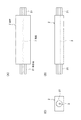
図1は、本技術に係る複合材料構造物の構成を説明する上面模式図である。また、図2及び図3は、本技術に係る複合材料構造物の構成を説明する断面模式図である。図2は図1中P−P断面に対応し、図3はQ−Q断面に対応する。
1. Composite Material Structure FIG. 1 is a schematic top view illustrating the configuration of a composite material structure according to the present technology. 2 and 3 are schematic cross-sectional views illustrating the configuration of the composite material structure according to the present technology. 2 corresponds to the PP cross section in FIG. 1, and FIG. 3 corresponds to the QQ cross section.
図中、符号Aで示す複合材料構造物は、熱圧着により接合された基材11、12と、基材中に埋め込まれて接合された埋め込み部材2(以下、単に「部材2」と称する)とから構成されている。基材11,12及び部材2には、領域3が形成されている。以下、領域3を液体が通流される流路として説明し、「流路3」と称するものとする。また、複合材料構造物Aを前記液体の分析に供されるマイクロチップとして説明し、「マイクロチップA」と称する。
In the figure, a composite material structure denoted by reference symbol A includes
基材11、12は、熱可塑性樹脂からなり、熱圧着により接合されている。基材11、12には、流路3の一部構成として、分析対象とする液体あるいは分析対象物を含む液体を外部から流路3内に導入するための導入口31と、該液体を流路3内から外部へ導出するための排出口32が形成されている。
The
熱可塑性樹脂としては、マイクロチップの材料として従来用いられている樹脂であってよく、ポリカーボネート、ポリメタクリル酸メチル樹脂(PMMA)、環状ポリオレフィン、ポリエチレン、ポリスチレン、ポリプロピレン及びポリメチルジシラザン(PDMS)などが挙げられる。基材11、12への流路3等の成形は、ナノインプリント、射出成型及び機械加工などの従来公知の手法によって行うことができる。
The thermoplastic resin may be a resin conventionally used as a material for a microchip, such as polycarbonate, polymethyl methacrylate resin (PMMA), cyclic polyolefin, polyethylene, polystyrene, polypropylene, and polymethyldisilazane (PDMS). Is mentioned. Molding of the
部材2は、基材11、12を構成する熱可塑性樹脂よりも熱変形温度が高い材料からなる。部材2の材料としては、上述の熱可塑性樹脂、金属、ガラス、石英、セラミック等が挙げられる。部材2への流路3等の成形は、例えば部材2がガラス製の場合、ウェットエッチングやドライエッチングによって行うことができる。また、例えば部材2が金属製の場合には、機械加工によって行えばよい。
The
流路3のうち、基材11、12に形成された部分と部材2に形成された部分とは、図1及び図2に示されるように、位置ずれを生じることなく連絡され、繋ぎ合わされている。これにより、流路3内に導入された液体が、基材11、12に形成された部分と部材2に形成された部分との繋ぎ目において流れに乱れを生じることなく流路3内を通流できるようにされている。
Of the
このような基材11、12に形成された流路3と部材2に形成された流路3との繋ぎ合わせは、熱圧着時に生じる基材11、12の熱変形を利用して、基材11,12に対して部材2を位置決めすることによって達成できる。すなわち、図3に示すように、マイクロチップAでは、部材2が熱変形により収縮した基材11,12の壁面13によって固定保持されることによって、基材11,12と部材2とが位置決めされている。基材11、12の熱変形を利用した基材11,12と部材2との位置決めについては、次の複合材料構造物の製造方法の項において詳しく説明する。
Such a connection between the
ここでは、マイクロチップAとして、二つの基材11,12と一つの部材2が複合化された複合材料構造物を例示したが、本技術に係る複合材料構造物は、基材を三以上含むものであってよく、部材も二以上含んでいてよい。また、ここでは、流路3等の領域が基材11,12のそれぞれに一部ずつ形成されてなる場合を例に説明したが、これらの領域は基材11,12のいずれか一方に全て形成されているものであってよい。
Here, as the microchip A, a composite material structure in which two
2.複合材料構造物の製造方法
次に、図4〜図6を参照して、上述のマイクロチップAを例に、本技術に係る複合材料構造物の製造方法について説明する。図4は、基材11,12の構成を説明する断面模式図であり、図2において部材2を省略した図に相当する。図5は、部材2の構成を説明する模式図であり、(A)は上面図、(B)は側面図、(C)は正面図を示す。図6は、基材11,12と部材2の接合部の構成を説明する断面模式図であり、(A)は基材11,12の熱変形前、(B)は熱変形後を示す。なお、図6は、図1中Q−Q断面に対応している。
2. Next, a method for manufacturing a composite material structure according to the present technology will be described with reference to the above-described microchip A as an example with reference to FIGS. 4 is a schematic cross-sectional view illustrating the configuration of the
まず、第一の工程として、熱可塑性樹脂からなり、空間14を有する基材11,12を配する工程について説明する。本工程では、基材11,12に、両者を重ね合わせた状態において部材2を挿入可能となる空間14を形成する(図4参照)。この空間14は、基材11、12の重ね合わせ時において、一面に流路3が開口し、これと対向する面が開放された直方体形状の空間とされている。空間14は、流路3と同様に、ナノインプリント、射出成型及び機械加工などの手法より成形される。
First, as a first step, a step of arranging
一方、部材2の両端には、基材11,12の空間14に挿入される係合端21が構成されている。係合端21は、直方体形状とされた部材2本体の両端に、正面視八角形(図5(C)参照)の柱体形状で設けられている。部材2本体及び二つの係合端21には、一本の流路3が形成されている。
On the other hand, engaging ends 21 to be inserted into the
次に、第二の工程として、空間14内に、前記熱可塑性樹脂よりも熱変形温度が高い材料からなる部材2を挿入する工程について説明する。本工程では、係合端21を、重ね合わされた基材11、12が形成する空間14に挿入する。空間14に係合端21が挿入された状態を、図6(A)に示す。空間14への係合端21の挿入は、基材11と基材12を重ね合わせた後、空間14に係合端21を挿し入れることによって行ってもよいが、好適には以下のようにして行うことができる。すなわち、まず、基材12の空間14を構成する凹部に部材2の係合端21を係止させる。次に、基材11の空間14を構成する凹部の位置と、基材12に係止させた係合端21との位置が一致するようにして、基材11を基材12に重ね合わせる。
Next, as a second step, a step of inserting the
空間14への係合端21の挿入を容易にするため、空間14の内径L1は、係合端21の外径lと同径か、あるいは外径lよりも若干大きく形成することが好ましい。ただし、空間14の内径L1を係合端21の外径lよりも大きく形成する場合にも、次に説明するように、基材11,12の熱圧着時に、熱変形した空間14を構成する壁面13が係合端21に接触できるようにする必要がある。なお、ここで、内径L1及び外径lは図中上下方向(Y軸方向)に限定して解釈されるものではなく、左右方向(X軸方向)を含めてあらゆる方向の径を意味すると解すべきである。
In order to facilitate the insertion of the
続いて、第三の工程として、基材11,12を熱圧着により接合することによって、空間14内に挿入された部材2を、熱変形した基材11,12の空間14を構成する壁面13によって固定保持させる工程について説明する。本工程では、空間14へ係合端21を挿入した後、基材11,12を熱圧着する。熱圧着は、基材11,12を構成する熱可塑性樹脂の熱変形温度よりも高く、部材2を構成する材料の熱変形温度よりも低い温度で行う。この熱圧着操作により、基材11,12は熱変形し、空間14を構成する壁面13が熱収縮し、空間14が縮小する。一方、部材2は、熱圧着操作によっても熱変形しない。その結果、熱変形後の空間14の内径L2が係合端21の外径lよりも小さくなり、図6(B)に示すように、熱収縮した壁面13によって係合端21が固定保持され、基材11,12と部材2が接合される。
Subsequently, as a third step, the
熱圧着操作の際、壁面13の熱収縮及び空間14の縮小は等方的に生じる。具体的には、空間14を構成する壁面13のうちY軸方向で対向する壁面131,132とX軸方向で対向する壁面133,134との4面は、熱収縮によって空間14側に等しく膨出してくる。その結果、等量膨出した壁面131,132,133,134によって、係合端21が空間14内の中央に保持され、位置決めされることになる。そして、基材11,12に形成された流路3の一部と部材2に形成された流路3の一部とが連絡され、繋ぎ合わされる(図1及び図2参照)。
During the thermocompression operation, the heat shrinkage of the
このように、基材11,12の熱収縮を利用して、空間14内の中央に部材2が保持固定されるようにすることで、基材11,12及び部材2にそれぞれ形成された流路3を簡便かつ高精度に位置決めでき、ずれを生じることなく繋ぎ合わせることが可能となる。
As described above, the
空間14の内径L1及び係合端21の外径lは、このような壁面13の熱収縮量を考慮して、熱収縮した壁面13が係合端21に密に接触できるように適切な径に設定される。すなわち、空間14の内径L1は、熱変形後の内径L2が係合端21の外径lよりも小さくなるように予め設計される。
Outer diameter l of the inner diameter L 1 and the
ここでは、熱収縮した壁面131,132,133,134によって係合端21が空間14内においてX軸方向及びY軸方向の両方向に位置決めされる場合を説明したが、位置決め方向は壁面131,132によってX軸方向にのみ、あるいは壁面133,134によってY軸方向のみの一方向になされてもよい。位置決めを一方向のみに行う場合、空間14の内径L1はX軸方向とY軸方向とで異なっていてもよく、係合端21の外径lも同様にX軸方向とY軸方向とで異なっていてよい。さらに、位置決め方向は、X軸方向及び/又はY軸方向に加えて、これらにZ軸方向(流路3に平行な方向)にも行うことが可能である。
Here, the case where the
また、熱収縮した際、壁面13の一部は係合端21に接触しないように、空間14の形状及び係合端21の形状を設計することが好ましい。熱収縮した際、壁面13の全面が係合端21に密接する場合、空間14側に膨張する熱可塑性樹脂の圧力によって部材2が変形、破壊されるおそれがある。これを回避するため、ここでは、空間14を直方体形状とし、係合端21を八角柱形状としている。これにより、空間14が熱縮小した場合に、係合端21の8面のうち4面は壁面13に接触せず、壁面13との間に空隙を形成することとなるため、この空隙が膨張した熱可塑性樹脂の逃げ場となって部材2に過度の圧力がかかることが防止される。
Moreover, it is preferable to design the shape of the
空間14及び係合端21の形状は、直方体形状と八角柱形状の組み合わせに限定されず、種々の形状の組み合わせであってよい。例えば図7(A)、(B)に示すように、係合端21の形状は、円柱であってもよい。また、例えば図7(C)、(D)に示すように、空間14を八角柱形状とし、係合端21を円柱形状としてもよい。いずれの場合にも、熱収縮した際、壁面13の一部は、係合端21に密接して空間14内に係合端21を位置決めするように機能し、かつ、壁面13の他の一部は係合端21との間に空隙を形成して部材2への過度の圧力を防止するように機能する。
The shape of the
基材11,12の熱変形により接合された基材11,12と部材2との接合部には、封止材を配したり、封止材による処理を行ったりして、液密性を高めるようにしてもよい。封止は、ゴム等の弾性部材(Oリングなど)を接合部に配する方法や、接着剤を接合部に塗布する方法などによって行うことができる。
A sealing material is disposed at the joint between the
3.微小粒子分析用マイクロチップ
上述したマイクロチップAの具体的な実施形態の一例として、マイクロチップAを微小粒子分析のために用いる例を説明する。なお、微小粒子分析用のマイクロチップとしては、先に挙げた特許文献1を参照可能である。
3. Microchip for microparticle analysis As an example of a specific embodiment of the microchip A described above, an example in which the microchip A is used for microparticle analysis will be described. As a microchip for analyzing microparticles, the above-mentioned Patent Document 1 can be referred to.
図8に示すマイクロチップAは、熱圧着により接合された熱可塑性樹脂製基材に、石英からなる部材2が埋め込まれてなり、基材と部材2には分析対象とする微小粒子を含む液体(以下、「サンプル液」と称する)が通流される流路3が形成されている。
The microchip A shown in FIG. 8 is formed by embedding a
サンプル液は、サンプルインレット311から流路3内に導入される。サンプル液に含まれる微小粒子は、細胞や微生物、リポソームなどの生体関連微小粒子、あるいはラテックス粒子やゲル粒子、工業用粒子などの合成粒子などであってよい。生体関連微小粒子には、各種細胞を構成する染色体、リポソーム、ミトコンドリア、オルガネラ(細胞小器官)などが含まれる。対象とする細胞には、動物細胞(血球系細胞など)および植物細胞が含まれる。微生物には、大腸菌などの細菌類、タバコモザイクウイルスなどのウイルス類、イースト菌などの菌類などが含まれる。さらに、生体関連微小粒子には、核酸やタンパク質、これらの複合体などの生体関連高分子も包含され得るものとする。また、工業用粒子は、例えば有機もしくは無機高分子材料、金属などであってもよい。有機高分子材料には、ポリスチレン、スチレン・ジビニルベンゼン、ポリメチルメタクリレートなどが含まれる。無機高分子材料には、ガラス、シリカ、磁性体材料などが含まれる。金属には、金コロイド、アルミなどが含まれる。これら微小粒子の形状は、一般には球形であるのが普通であるが、非球形であってもよく、また大きさや質量なども特に限定されない。
The sample liquid is introduced into the
サンプル液は、シースインレット312から導入されるシース液により周囲を取り囲まれた状態で流路3を送液される。シースインレット312から導入されたシース液は、2方向に分かれて送液された後、サンプルインレット311から導入されたサンプル液との合流部において、サンプル液を2方向から挟み込むようにしてサンプル液に合流する。これにより、合流部において、シース液層流の中央にサンプル液層流が位置された3次元層流が形成される。
The sample liquid is sent through the
符号4は、流路3に詰まりや気泡が生じた際に、流路3内に負圧を加えて流れを一時的に逆流させて詰まりや気泡を解消するための吸引流路を示す。吸引流路4の一端には、真空ポンプ等の負圧源が接続される吸引アウトレット42が形成され、他端は連通口41において流路3に接続している。
Reference numeral 4 indicates a suction flow path for eliminating clogging or bubbles by applying a negative pressure in the
微小粒子は、形成された3次元層流中に一列に配列した状態となって流路3内を通流され、光学検出手段Bによる光照射部まで送液される。光学検出手段Bは、レーザー光源、微小粒子に対してレーザー光を集光・照射する集光レンズ、ダイクロイックミラー、バンドパスフィルターなどからなる照射系と、レーザー光の照射によって微小粒子から発生する測定対象光を検出する検出系と、によって構成される。検出系は、例えば、PMT(photo multiplier tube)や、CCD及びCMOS素子等のエリア撮像素子などによって構成される。なお、図では、光学検出手段Bとして集光レンズのみを示した。また、図では、照射系と検出系を同一の光学経路により構成した場合を示したが、照射系と検出系は別個の光学経路により構成してもよい。
The fine particles are arranged in a line in the formed three-dimensional laminar flow, flow through the
光学検出手段Bの検出系により検出される測定対象光は、測定光の照射によって微小粒子から発生する光であって、例えば、前方散乱光や側方散乱光、レイリー散乱やミー散乱等の散乱光や蛍光などとすることができる。これらの測定対象光は電気信号に変換され、この電気信号に基づいて微小粒子の光学特性が検出される。 The measurement target light detected by the detection system of the optical detection means B is light generated from the microparticles by irradiation of the measurement light. For example, forward scattered light, side scattered light, Rayleigh scattered light, Mie scattered light, etc. It can be light or fluorescence. These measurement target lights are converted into electrical signals, and the optical characteristics of the microparticles are detected based on the electrical signals.
光照射部を通過したサンプル液は、流路3の一端に設けられた吐出口321からチップ外の空間に排出される。この際、振動素子によってマイクロチップAを振動させることで、サンプル液を微小粒子を含む液滴としてチップ外の空間に吐出できる。吐出された液滴には、荷電電極インレット5に挿入された電極によって電荷が付与される。
The sample liquid that has passed through the light irradiation unit is discharged from a discharge port 321 provided at one end of the
チップ外の空間には、吐出された液滴の移動方向に沿って、移動する液滴を挟んで対向する対電極配置されており、この対電極との電気的な反発力(又は吸引力)によって液滴の移動方向が制御されることによって、液滴に含まれる微小粒子がその光学特性に応じて分別、分取される。 In the space outside the chip, a counter electrode is arranged opposite to the moving droplet along the moving direction of the discharged droplet, and an electric repulsive force (or suction force) with the counter electrode is arranged. By controlling the moving direction of the liquid droplets, the fine particles contained in the liquid droplets are sorted and sorted according to their optical characteristics.
マイクロチップAでは、流路3のうち光学検出手段Bによる光照射部を構成する部分を、光透過性に優れ、光学誤差の少ない石英によって形成している。このため、微小粒子へのレーザー光の照射効率が高く、測定対象光も高精度に検出することでき、微小粒子の光学特性を正確に判定して分取を行うことが可能である。
In the microchip A, the portion of the
また、マイクロチップAの光照射部のみを高価な石英とし、他の部分は安価で成形が容易な熱可塑性樹脂によって構成することで、チップ全体の製造コストを抑制することも可能である。なお、部材2の材料は、光透過性に優れ、光学誤差の少ない材料であれば、石英に限定されることはない。
Moreover, it is also possible to suppress the manufacturing cost of the whole chip by making only the light irradiation part of the microchip A expensive quartz and making the other parts by a thermoplastic resin that is inexpensive and easy to mold. The material of the
基材と部材2にそれぞれに形成された流路3は、上述した本技術に係る複合材料構造物の製造方法を適用することによって、位置ずれを生じることなく連絡し、繋ぎ合わされている。例えば、流路3の径が100μmである場合、本技術に係る複合材料構造物の製造方法によれば、数十μm以下の位置決め精度で流路を繋ぎ合わせることができる。
The
このため、マイクロチップAでは、流路3内に形成されたサンプル液とシース液との3次元層流が、基材に形成された部分と部材2に形成された部分との繋ぎ目において乱れることなく流路3内を通流できる。従って、マイクロチップAでは、光照射部におけるレーザー光の焦点位置と微小粒子の送流位置を精緻に一致させて、微小粒子の光学特性を正確に測定することができる。また、吐出口321からチップ外の空間に排出される液滴の形状及び大きさを安定化して、液滴の移動方向の制御及び分取を高精度に行うことができる。
For this reason, in the microchip A, the three-dimensional laminar flow of the sample liquid and the sheath liquid formed in the
本技術に係る複合材料構造物は以下のような構成をとることもできる。
(1)熱可塑性樹脂からなり、熱圧着により接合された二以上の基材と、前記熱可塑性樹脂よりも熱変形温度が高い材料からなり、前記基材の少なくとも一つに形成された空間内に挿入された一以上の部材と、から構成され、前記空間内に挿入された前記部材が、熱圧着により熱変形した前記基材の前記空間を構成する壁面によって固定保持されている複合材料構造物。
(2)前記空間内における前記部材の位置が前記壁面によって位置決めされている上記(1)記載の複合材料構造物。
(3)前記基材の少なくとも一以上と前記部材とにそれぞれ形成された領域が連絡するように、前記部材が前記空間内に位置決めされている上記(1)又は(2)記載の複合材料構造物。
(4)前記領域として液体が通流される流路が形成されたマイクロチップである上記(3)記載の複合材料構造物。
(5)前記流路を通流する液体あるいは該液体に含まれる試料に対して光が照射される光照射部を備え、前記基材を構成する前記熱可塑性樹脂よりも光透過性に優れた材料からなる前記部材によって、前記光照射部が構成されている上記(4)記載の複合材料構造物。
The composite material structure according to the present technology may have the following configuration.
(1) Two or more base materials made of a thermoplastic resin, joined by thermocompression bonding, and a material having a higher heat deformation temperature than the thermoplastic resin, and formed in at least one of the base materials And a composite material structure in which the member inserted into the space is fixed and held by a wall surface constituting the space of the base material that is thermally deformed by thermocompression bonding. object.
(2) The composite material structure according to (1), wherein the position of the member in the space is positioned by the wall surface.
(3) The composite material structure according to the above (1) or (2), wherein the member is positioned in the space so that at least one of the substrates and regions formed in the member communicate with each other. object.
(4) The composite material structure according to the above (3), which is a microchip in which a channel through which a liquid flows is formed as the region.
(5) A light irradiating part for irradiating light to the liquid flowing through the flow path or the sample contained in the liquid is provided, and the light transmission is superior to the thermoplastic resin constituting the substrate. The composite material structure according to the above (4), wherein the light irradiation part is constituted by the member made of a material.
また、本技術に係る複合材料構造物の製造方法は以下のような構成をとることもできる。
(1)熱可塑性樹脂からなり、少なくとも一つに形成された空間を有する二以上の基材を配する工程と、前記空間内に、前記熱可塑性樹脂よりも熱変形温度が高い材料からなる一以上の部材を挿入する工程と、前記基材を熱圧着により接合することによって、前記空間内に挿入された前記部材を、熱変形した前記基材の前記空間を構成する壁面によって固定保持させる工程と、を含む複合材料構造物の製造方法。
(2)前記固定保持させる工程において、前記空間内における前記部材の位置を前記壁面によって位置決めする上記(1)記載の製造方法。
(3)前記固定保持させる工程において、前記基材の少なくとも一以上と前記部材とにそれぞれ形成された領域が連絡するように、前記部材を前記空間内に位置決めする上記(1)又は(2)記載の製造方法。
(4)前記固定保持させる工程において、前記基材を構成する前記熱可塑性樹脂の熱変形温度よりも高く、かつ、前記部材を構成する材料の熱変形温度よりも低い温度で、前記基材の熱圧着を行う上記(1)〜(3)のいずれかに記載の製造方法。
Moreover, the manufacturing method of the composite material structure which concerns on this technique can also take the following structures.
(1) A step of arranging two or more base materials made of a thermoplastic resin and having a space formed in at least one; and a material made of a material having a higher thermal deformation temperature than the thermoplastic resin in the space. The step of inserting the above members, and the step of fixing and holding the member inserted into the space by the wall surface constituting the space of the base material thermally deformed by joining the base material by thermocompression bonding. And a method for manufacturing a composite material structure.
(2) The manufacturing method according to (1), wherein in the step of fixing and holding, the position of the member in the space is positioned by the wall surface.
(3) In the step of fixing and holding, the member is positioned in the space so that at least one of the base materials and the region formed on the member are in contact with each other (1) or (2) The manufacturing method as described.
(4) In the step of fixing and holding, at a temperature higher than the heat deformation temperature of the thermoplastic resin constituting the base material and lower than the heat deformation temperature of the material constituting the member, The manufacturing method in any one of said (1)-(3) which performs thermocompression bonding.
本技術に係る複合材料構造物及びその製造方法によれば、異種材料からなる複数の部材を簡便かつ高精度に位置決めして複合化させることができ、部材の熱収縮を利用して複合化を行うことで部材の公差に対する許容度を大きくできる。このため、本技術は、成形の容易性等などの製造工程上の制約及び光透過性などの機能上の制約から異種材料からなる部材を複合化させて構造物を得る際に有用であり、例えば高機能な光学用途の構造物を構成するために利用できる。 According to the composite material structure and the manufacturing method thereof according to the present technology, a plurality of members made of different materials can be easily and accurately positioned and combined, and the heat shrinkage of the members can be used to combine them. By doing so, the tolerance for the tolerance of the member can be increased. For this reason, the present technology is useful in obtaining a structure by combining members made of different materials from restrictions on manufacturing processes such as ease of molding and functional restrictions such as light transmittance, For example, it can be used to construct a highly functional optical structure.
A:マイクロチップ、B:光学検出手段、11,12:基材、13,131,132,133,134:壁面、14:空間、2:埋め込み部材、21:係合端、3:流路、31:導入口、311:サンプルインレット、312:シースインレット、32:排出口、321:吐出口、4:吸引流路、41:連通口、42:吸引アウトレット、5:荷電電極インレット A: microchip, B: optical detection means, 11, 12: base material, 13, 131, 132, 133, 134: wall surface, 14: space, 2: embedded member, 21: engagement end, 3: flow path, 31: introduction port, 311: sample inlet, 312: sheath inlet, 32: discharge port, 321: discharge port, 4: suction channel, 41: communication port, 42: suction outlet, 5: charged electrode inlet
Claims (10)
前記熱可塑性樹脂よりも熱変形温度が高い材料からなり、前記基材の少なくとも一つが有する空間内に挿入されている一以上の部材と、から構成され、
前記基材のうち少なくとも一つと前記部材のそれぞれに液体が通流される流路が形成されており、
前記流路を通流する前記液体あるいは前記液体に含まれる試料に対して光が照射される光照射部を備え、
前記空間内に挿入されている前記部材が、熱圧着により熱変形した前記基材の前記空間を構成する壁面によって固定保持されているマイクロチップ。 Two or more substrates made of thermoplastic resin and joined by thermocompression bonding;
It is made of a material having a higher heat distortion temperature than the thermoplastic resin, and is composed of one or more members inserted into a space of at least one of the base materials,
A flow path through which a liquid flows is formed in each of at least one of the substrates and the member,
A light irradiation unit for irradiating light to the liquid flowing through the flow path or a sample contained in the liquid ;
The microchip in which the member inserted into the space is fixed and held by a wall surface constituting the space of the base material that is thermally deformed by thermocompression bonding .
前記空間内に、前記熱可塑性樹脂よりも熱変形温度が高い材料からなる一以上の部材を挿入する工程と、
前記基材を熱圧着により接合することによって、前記空間内に挿入された前記部材を、熱変形した前記基材の前記空間を構成する壁面によって固定保持させる工程と、
を含み、
前記固定保持させる工程において、前記基材の少なくとも一以上と前記部材とにそれぞれ形成された流路が連絡するように、前記部材を前記空間内に位置決めするマイクロチップの製造方法。 A step of arranging two or more base materials made of a thermoplastic resin and having a space formed in at least one;
Inserting one or more members made of a material having a higher thermal deformation temperature than the thermoplastic resin into the space;
A step of fixing and holding the member inserted into the space by a wall surface constituting the space of the base material that has been thermally deformed by joining the base material by thermocompression bonding;
Including
A method of manufacturing a microchip, wherein in the fixing and holding step, the member is positioned in the space so that at least one of the base members and a channel formed in the member communicate with each other.
In the step of fixing and holding, the base material is subjected to thermocompression bonding at a temperature higher than the heat deformation temperature of the thermoplastic resin constituting the base material and lower than the heat deformation temperature of the material constituting the member. the process according to any one of claims 7-9 carried out.
Priority Applications (8)
| Application Number | Priority Date | Filing Date | Title |
|---|---|---|---|
| JP2011158723A JP5974429B2 (en) | 2011-07-20 | 2011-07-20 | Composite material structure and manufacturing method thereof |
| IN261DEN2014 IN2014DN00261A (en) | 2011-07-20 | 2012-06-15 | |
| EP12731185.0A EP2734361B1 (en) | 2011-07-20 | 2012-06-15 | Composite structure and manufacturing method therefor |
| CN201280034743.XA CN103702826B (en) | 2011-07-20 | 2012-06-15 | Complex structure body and manufacture method thereof |
| CN201510420058.6A CN105126940B (en) | 2011-07-20 | 2012-06-15 | Complex structure body and the microchip for analyzing particulate |
| PCT/JP2012/003939 WO2013011629A1 (en) | 2011-07-20 | 2012-06-15 | Composite structure and manufacturing method therefor |
| US14/131,730 US9610750B2 (en) | 2011-07-20 | 2012-06-15 | Composite structure and manufacturing method therefor |
| US15/444,906 US10414118B2 (en) | 2011-07-20 | 2017-02-28 | Microchip manufactured with thermocompression |
Applications Claiming Priority (1)
| Application Number | Priority Date | Filing Date | Title |
|---|---|---|---|
| JP2011158723A JP5974429B2 (en) | 2011-07-20 | 2011-07-20 | Composite material structure and manufacturing method thereof |
Publications (3)
| Publication Number | Publication Date |
|---|---|
| JP2013022804A JP2013022804A (en) | 2013-02-04 |
| JP2013022804A5 JP2013022804A5 (en) | 2014-07-31 |
| JP5974429B2 true JP5974429B2 (en) | 2016-08-23 |
Family
ID=46420487
Family Applications (1)
| Application Number | Title | Priority Date | Filing Date |
|---|---|---|---|
| JP2011158723A Active JP5974429B2 (en) | 2011-07-20 | 2011-07-20 | Composite material structure and manufacturing method thereof |
Country Status (6)
| Country | Link |
|---|---|
| US (2) | US9610750B2 (en) |
| EP (1) | EP2734361B1 (en) |
| JP (1) | JP5974429B2 (en) |
| CN (2) | CN103702826B (en) |
| IN (1) | IN2014DN00261A (en) |
| WO (1) | WO2013011629A1 (en) |
Families Citing this family (2)
| Publication number | Priority date | Publication date | Assignee | Title |
|---|---|---|---|---|
| CN108393103A (en) * | 2018-03-03 | 2018-08-14 | 北京工业大学 | A kind of achievable drop size does not depend on the micro-fluidic chip of flow |
| US11665929B2 (en) * | 2019-06-13 | 2023-05-30 | Intel Corporation | Micro light-emitting diode displays with improved power efficiency |
Family Cites Families (22)
| Publication number | Priority date | Publication date | Assignee | Title |
|---|---|---|---|---|
| JPH0524516Y2 (en) * | 1987-04-21 | 1993-06-22 | ||
| JPH03156888A (en) * | 1989-08-28 | 1991-07-04 | Toshiba Corp | Dispersion type el panel and manufacture thereof |
| GB8926294D0 (en) * | 1989-11-21 | 1990-01-10 | British Gas Plc | Method of jointing hollow members by fusion |
| US5427663A (en) | 1993-06-08 | 1995-06-27 | British Technology Group Usa Inc. | Microlithographic array for macromolecule and cell fractionation |
| GB9418981D0 (en) | 1994-09-21 | 1994-11-09 | Univ Glasgow | Apparatus and method for carrying out analysis of samples |
| JP3388392B2 (en) * | 1999-06-02 | 2003-03-17 | 日精樹脂工業株式会社 | IC card manufacturing equipment |
| WO2002028532A2 (en) * | 2000-10-06 | 2002-04-11 | Protasis Corporation | Microfluidic substrate assembly and method for making same |
| US6564475B2 (en) * | 2000-12-22 | 2003-05-20 | K-Swiss Inc. | Footwear with enhanced temperature control |
| AU2003293399A1 (en) | 2002-12-04 | 2004-06-23 | Spinx, Inc. | Devices and methods for programmable microscale manipulation of fluids |
| WO2004081555A1 (en) * | 2003-03-14 | 2004-09-23 | Nec Corporation | Mass spectrometric system and mass spectrometry |
| JP4695851B2 (en) * | 2003-07-10 | 2011-06-08 | シチズンホールディングス株式会社 | Micro chemical chip temperature controller |
| JP4304120B2 (en) * | 2004-04-30 | 2009-07-29 | ベイバイオサイエンス株式会社 | Apparatus and method for sorting biological particles |
| CN1687766A (en) | 2005-04-21 | 2005-10-26 | 复旦大学 | Fibrous electrophoresis chip and preparation method |
| CN101175572A (en) * | 2005-05-19 | 2008-05-07 | 皇家飞利浦电子股份有限公司 | Functional assembly and method of obtaining it |
| JP4695977B2 (en) * | 2005-12-21 | 2011-06-08 | 東ソー・クォーツ株式会社 | Microchip and manufacturing method thereof |
| JP2007263706A (en) * | 2006-03-28 | 2007-10-11 | Aisin Seiki Co Ltd | Microchip for bioassay |
| US8312646B2 (en) * | 2006-05-25 | 2012-11-20 | Nike, Inc. | Article of footwear incorporating a tensile element |
| EP1972909A1 (en) | 2007-03-23 | 2008-09-24 | Koninklijke Philips Electronics N.V. | Luminescence sensor |
| US7880108B2 (en) * | 2007-10-26 | 2011-02-01 | Becton, Dickinson And Company | Deflection plate |
| JP2009243965A (en) * | 2008-03-28 | 2009-10-22 | Sumitomo Bakelite Co Ltd | Flow path device, flow path device with exterior case, method for using flow path device |
| JP4572973B2 (en) * | 2008-06-16 | 2010-11-04 | ソニー株式会社 | Microchip and flow-feeding method in microchip |
| JP5487638B2 (en) | 2009-02-17 | 2014-05-07 | ソニー株式会社 | Apparatus for microparticle sorting and microchip |
-
2011
- 2011-07-20 JP JP2011158723A patent/JP5974429B2/en active Active
-
2012
- 2012-06-15 US US14/131,730 patent/US9610750B2/en active Active
- 2012-06-15 WO PCT/JP2012/003939 patent/WO2013011629A1/en active Application Filing
- 2012-06-15 CN CN201280034743.XA patent/CN103702826B/en active Active
- 2012-06-15 IN IN261DEN2014 patent/IN2014DN00261A/en unknown
- 2012-06-15 EP EP12731185.0A patent/EP2734361B1/en not_active Not-in-force
- 2012-06-15 CN CN201510420058.6A patent/CN105126940B/en active Active
-
2017
- 2017-02-28 US US15/444,906 patent/US10414118B2/en active Active
Also Published As
| Publication number | Publication date |
|---|---|
| EP2734361A1 (en) | 2014-05-28 |
| CN105126940B (en) | 2018-05-18 |
| US10414118B2 (en) | 2019-09-17 |
| IN2014DN00261A (en) | 2015-06-05 |
| US9610750B2 (en) | 2017-04-04 |
| EP2734361B1 (en) | 2017-08-09 |
| CN103702826A (en) | 2014-04-02 |
| CN103702826B (en) | 2015-08-19 |
| US20140154475A1 (en) | 2014-06-05 |
| WO2013011629A1 (en) | 2013-01-24 |
| JP2013022804A (en) | 2013-02-04 |
| CN105126940A (en) | 2015-12-09 |
| US20170203296A1 (en) | 2017-07-20 |
Similar Documents
| Publication | Publication Date | Title |
|---|---|---|
| JP6003020B2 (en) | Microchip and fine particle analyzer | |
| JP4661942B2 (en) | Microchip and its channel structure | |
| JP4572973B2 (en) | Microchip and flow-feeding method in microchip | |
| KR101850548B1 (en) | Microparticle sorting apparatus, microchip module, and method of sorting microparticles | |
| EP2191895B1 (en) | Microparticle analysis device, microfluidic chip for microparticle analysis, and microparticle analysis method | |
| WO2005108963A1 (en) | Microfluidic cell sorter system | |
| KR20130045236A (en) | Microchip and particulate analyzing device | |
| JP2018151319A (en) | Microchip and microparticle measuring apparatus | |
| JP5974429B2 (en) | Composite material structure and manufacturing method thereof | |
| JP5316530B2 (en) | Microchip and its channel structure | |
| CN107427831B (en) | Microchip, analysis device, and analysis method | |
| JP5092881B2 (en) | Channel structure and microchip | |
| WO2021100618A1 (en) | Microchip, sample isolation kit, and microparticle isolation device | |
| WO2022185980A1 (en) | Particle fractionating kit | |
| WO2019230489A1 (en) | Microchip and sample isolation kit | |
| JP2013250229A (en) | Microchip for microparticle fractionation, microparticle fractionation device mounted with microchip for microparticle fractionation, and fractionation method for microparticle |
Legal Events
| Date | Code | Title | Description |
|---|---|---|---|
| A521 | Written amendment |
Free format text: JAPANESE INTERMEDIATE CODE: A523 Effective date: 20140617 |
|
| A621 | Written request for application examination |
Free format text: JAPANESE INTERMEDIATE CODE: A621 Effective date: 20140617 |
|
| A131 | Notification of reasons for refusal |
Free format text: JAPANESE INTERMEDIATE CODE: A131 Effective date: 20150901 |
|
| A521 | Written amendment |
Free format text: JAPANESE INTERMEDIATE CODE: A523 Effective date: 20151030 |
|
| A131 | Notification of reasons for refusal |
Free format text: JAPANESE INTERMEDIATE CODE: A131 Effective date: 20160308 |
|
| A521 | Written amendment |
Free format text: JAPANESE INTERMEDIATE CODE: A523 Effective date: 20160420 |
|
| TRDD | Decision of grant or rejection written | ||
| A01 | Written decision to grant a patent or to grant a registration (utility model) |
Free format text: JAPANESE INTERMEDIATE CODE: A01 Effective date: 20160621 |
|
| A61 | First payment of annual fees (during grant procedure) |
Free format text: JAPANESE INTERMEDIATE CODE: A61 Effective date: 20160704 |
|
| R151 | Written notification of patent or utility model registration |
Ref document number: 5974429 Country of ref document: JP Free format text: JAPANESE INTERMEDIATE CODE: R151 |
|
| R250 | Receipt of annual fees |
Free format text: JAPANESE INTERMEDIATE CODE: R250 |
|
| R250 | Receipt of annual fees |
Free format text: JAPANESE INTERMEDIATE CODE: R250 |