JP5973766B2 - Image processing device - Google Patents
Image processing device Download PDFInfo
- Publication number
- JP5973766B2 JP5973766B2 JP2012079529A JP2012079529A JP5973766B2 JP 5973766 B2 JP5973766 B2 JP 5973766B2 JP 2012079529 A JP2012079529 A JP 2012079529A JP 2012079529 A JP2012079529 A JP 2012079529A JP 5973766 B2 JP5973766 B2 JP 5973766B2
- Authority
- JP
- Japan
- Prior art keywords
- image data
- data
- pixel region
- processing apparatus
- image processing
- Prior art date
- Legal status (The legal status is an assumption and is not a legal conclusion. Google has not performed a legal analysis and makes no representation as to the accuracy of the status listed.)
- Active
Links
Images


Classifications
-
- H—ELECTRICITY
- H04—ELECTRIC COMMUNICATION TECHNIQUE
- H04N—PICTORIAL COMMUNICATION, e.g. TELEVISION
- H04N23/00—Cameras or camera modules comprising electronic image sensors; Control thereof
- H04N23/80—Camera processing pipelines; Components thereof
Landscapes
- Engineering & Computer Science (AREA)
- Multimedia (AREA)
- Signal Processing (AREA)
- Color Television Image Signal Generators (AREA)
- Color Television Systems (AREA)
- Processing Of Color Television Signals (AREA)
Description
本発明は画像処理装置に関し、特に、画像データの伝送データを生成する画像データの処理に関する。 The present invention relates to an image processing apparatus, and more particularly to image data processing for generating transmission data of image data.
従来、ベイヤー(Bayer)構造の画素配列を有する撮像素子を用いた撮像装置が一般に知られている。このような撮像素子は、色フィルタを介して画素を構成する光電変換素子に被写体からの像光を取り込み、像光の強さに応じて画像信号を出力する。そして、後段の処理部が画像信号に所定の処理を施すことによって、ビューファインダや外部の表示装置に画像を表示している。撮像素子には、一般にR,G,B信号をそれぞれ出力可能なR,G,B画素が所定のパターンで配置されている。 2. Description of the Related Art Conventionally, an image pickup apparatus using an image pickup element having a Bayer structure pixel array is generally known. Such an image sensor captures image light from a subject into a photoelectric conversion element that constitutes a pixel via a color filter, and outputs an image signal according to the intensity of the image light. Then, the subsequent processing unit performs predetermined processing on the image signal, thereby displaying an image on the viewfinder or an external display device. Generally, R, G, and B pixels that can output R, G, and B signals, respectively, are arranged in a predetermined pattern on the image sensor.
また、ベイヤー構造の撮像素子により得られた動画データを輝度信号と色差信号に変換し、SMPTE(Societyof Motion Picture and Television Engineers)に提案されているHD−SDI規格(SMPTE 274M)に従って伝送する装置も提案されている(例えば、特許文献1参照)。 In addition, there is also an apparatus that converts moving image data obtained by an image pickup device having a Bayer structure into a luminance signal and a color difference signal and transmits them in accordance with the HD-SDI standard (SMPTE 274M) proposed in SMPTE (Society of Motion Picture and Television Engineers). It has been proposed (see, for example, Patent Document 1).
特許文献1では、動画データを輝度と色差のデータに変換して送信しており、ベイヤー構造の動画データを送信することができなかった。また、HD−SDIのような規格に従ってベイヤー構造の動画データを伝送した場合、受信側では適宜RGBの信号を輝度と色差のデータに変換する処理が行われる。この際、良好に変換処理を行うためには、画素配列の有効画素領域の外側の画素のデータ(周辺画素データ)が必要となる。
In
本発明は、上記の問題点を鑑みてなされたものである。特に、ベイヤー構造の撮像素子から出力された動画データを送信する際に、この動画データを処理するために必要な画素の情報を適宜送信することができる伝送データの生成を目的とする。 The present invention has been made in view of the above problems. In particular, when transmitting moving image data output from an image sensor having a Bayer structure, an object is to generate transmission data that can appropriately transmit pixel information necessary for processing the moving image data.
本発明の一つの実施形態によれば、画像処理装置は、動画データを取得する取得手段と、前記動画データの有効画素領域の画像データを送信するための送信方式に従い、前記取得手段により取得された前記動画データから前記有効画素領域の画像データを含むデータストリームを生成する手段であって、前記有効画素領域の画像データに対し、前記有効画素領域の周辺の画素領域の画像データと、前記周辺の画素領域の画像データが多重されている位置に関する位置情報と、を多重することにより、前記データストリームを生成する生成手段と、前記生成手段により生成された前記データストリームを送信する送信手段とを備える。
According to one embodiment of the present invention, the image processing apparatus is acquired by the acquisition unit according to an acquisition unit that acquires moving image data and a transmission method for transmitting image data of an effective pixel area of the moving image data. Means for generating a data stream including image data of the effective pixel area from the moving image data, wherein the image data of the pixel area around the effective pixel area and the periphery of the image data of the effective pixel area; And generating means for generating the data stream by multiplexing the position information on the position where the image data of the pixel area is multiplexed, and transmitting means for transmitting the data stream generated by the generating means Prepare.
本発明によれば、HD−SDI規格に従ったベイヤーフォーマットの動画データの伝送において、色補間処理で利用する周辺画素の情報を動画データ上の所定の位置に多重化できるので、送信先が受信した動画データを正確に処理することが可能となる。 According to the present invention, in transmission of moving image data in the Bayer format in accordance with the HD-SDI standard, information on peripheral pixels used in color interpolation processing can be multiplexed at a predetermined position on the moving image data, so that the transmission destination can receive it. It is possible to accurately process the moving image data.
以下、添付図面を参照して本発明の実施形態を詳細に説明する。 Hereinafter, embodiments of the present invention will be described in detail with reference to the accompanying drawings.
図1は、本実施例に係わる撮像装置の構成例を示すブロック図である。実施例の撮像装置は、ベイヤー構造の動画データをSDI規格に従って送信する際に、有効領域の周辺の画素(以下、周辺画素と呼ぶ)を多重し、その画素のフレーム内における位置と信号の多重位置を特定できる情報を合わせて伝送する構成を備える。従って、本装置は撮像装置であるとともに画像データの送信装置(データ送信装置)でもある。 FIG. 1 is a block diagram illustrating a configuration example of an imaging apparatus according to the present embodiment. The image pickup apparatus according to the embodiment multiplexes pixels around the effective area (hereinafter referred to as peripheral pixels) when transmitting Bayer-structured moving image data in accordance with the SDI standard, and multiplexes the position of the pixel in the frame and the signal. It has a configuration for transmitting information that can specify the position together. Therefore, this apparatus is not only an imaging apparatus but also an image data transmission apparatus (data transmission apparatus).
図1において、撮像部101は、撮像レンズ102、シャッター103、撮像素子104、前置処理回路105、A/D変換器106、ROM107から構成される。撮像レンズ102は、ズームレンズおよびフォーカスレンズを含む。シャッター103は絞り機能を兼用している。
In FIG. 1, the
撮像素子104はCCDセンサやCMOSセンサなどによって図2に示すようなベイヤー構造のカラーフィルタを配した画素配列を有し、光学像を電気信号に変換する。撮像素子104は、後述する制御部112から供給されるクロックのタイミング(本実施例では、1/30秒)で、画素に蓄積された電荷量を示す電気信号をプログレッシブで前置処理回路105に供給する。前置処理回路105は、撮像素子104の出力ノイズ除去のためのCDS(相関2重サンプリング)回路やAGC(自動利得制御)回路を含む。前置処理回路105は撮像素子からの電気信号を入力し、A/D変換器106は前置処理回路105から出力されるアナログ信号をデジタル信号に変換する。
The
後置処理回路107は、A/D変換器106から供給された画像データをR、Gr、Gb、B(赤、緑、緑、青)の4つの画素プレーンに分離する。そして、それぞれの成分に色再現のリニアマトリックス処理を適用した後、各色10ビットの画素データを信号処理部109に供給する。
The
ROM108には、撮像素子104に関する情報として、総画素数、縦横のサイズ、有効ピクセルの位置などを記録している。
The
信号処理部109は、供給されたR、Gr、Gb、Bの画素データに対して後述の処理を施し、送信するのに適した形式のデータを生成してメモリ114に記憶する。マルチプレクサ110は、メモリ114より送信するデータを読み出して多重し、外部インターフェース111に送る。外部IF111は、SDI規格に従って動画データを外部に送信する。
The
制御部112はCPUを備え、フラッシュメモリ113に記憶された制御用のソフトウェアに従って撮像装置100の各部を制御する。制御部112は、操作部115からの入力を検出し、撮像部101、信号処理部109、マルチプレクサ110を、タイミングの同期をとりながら制御する。制御部112は各種処理で作成したデータを一時的にメモリ114に記録し、必要に応じてそれらを読み出す。フラッシュメモリ113は電気的に消去・記録可能であり、制御部112を動作させるために必要なプログラムや撮像装置100固有の調整データ等があらかじめ書き込まれている。表示制御部117は、撮像部101より得られたベイヤー構造の動画データにディベイヤー(DeBayer)処理等の所定の処理を施して表示用の動画データを生成し、表示部118に送る。表示部118は撮影された動画データを表示する。以上で説明した各構成は、各要素間の制御信号やデータ信号のための伝送路である内部バス116と接続されている。
The
このような撮像装置100において、操作部115より電源が投入されると、制御部112は各部を制御し、撮像部101より撮影された画像データを表示部118に表示して撮影待機状態とする。撮影待機状態において、操作部115より撮影開始の指示があると、制御部112は以下の様に各部を制御し、撮影された画像データを外部IF111より出力する。そして、撮影停止の指示があると、制御部112は、外部IF111からの画像データの出力を停止する。
In such an
図3は、信号処理部109の構成を示している。メモリ303は、撮像部101の後置処理回路107から受け取った各色の画素のデータを一時的に記憶する(画像データ取得手段)。クロック供給部302は、後置処理回路107に対して画素のデータの読み出しクロックを供給する。後置処理回路107からメモリ303に供給される画素データは、制御部112により、有効画素のデータと、周辺画素のデータとを分けてメモリ303に記憶される。読出し部301は、メモリ303から画素のデータを読み出し、信号多重部304にそれを供給する。なお、メモリ303として、メモリ114の記憶領域の一部を利用することも可能である。
FIG. 3 shows the configuration of the
信号多重部304は、供給された画素データを伝送に適した順に並び替え、タイミング基準信号SAV(Start of Active Video)/EAV(End of Active Video)を多重し、さらに各種アンシラリー(ancillary)データを多重したデータストリームを生成する。
The
次に、制御部112が後置処理回路107から供給された画素データをメモリ303に記録するときの動作について説明する。
Next, an operation when the
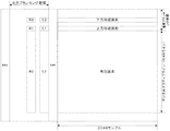
例えば、撮像素子104上の画素領域が図4の画素配置で構成されている場合について説明する。図4に示すように、撮像素子104は、有効画素領域と周辺画素領域から構成される。この画素配列の全体エリアから1回に取得可能な画素データ群をRAWフレームと定義する。RAWフレームの水平方向(横方向)の画素数が4112画素(4096+8+8)、垂直方向(縦方向)の画素数は2176画素(2160+8+8)であり、ベイヤー構造で画素が配列される。
For example, the case where the pixel region on the
制御部112は、ROM108から上記のような画素配列の縦横幅や各エリアの位置の情報、そしてベイヤー構造の各画素の配列方法に関する情報などを読み込む。制御部112は、撮像素子104に関する情報により記録のタイミングの制御を行い、後置処理回路107から供給される信号から、有効画素のデータと周辺画素のデータのそれぞれを異なる領域に分けてメモリ303に記録する。
The
図5は、制御部112がRAM303に記録する、RAWフレームを構成する有効画素領域の各色(R、Gr、Gb、B)の画素データである。各色の画素群は、水平方向が2048画素、垂直方向が1080画素である。また、制御部112は、図4で示した8つのエリア(上方、下方、左側(L1、L2、L3)、右側(R1、R2、R3))に位置している周辺画素のデータを、有効画素領域の画素データとは識別可能な状態でメモリ303に記憶する。
FIG. 5 shows pixel data of each color (R, Gr, Gb, B) in the effective pixel area constituting the RAW frame, which is recorded in the
このとき制御部112は、図6で示すデータテーブルを作成し、周辺画素のデータに関連づけてメモリ114に記憶する。このデータテーブルは、RAWフレームにおける各周辺画素のデータの位置と、周辺画素のデータを伝送するときの伝送信号への多重位置の設定値とを示す。制御部112は(情報取得手段)、RAWフレームの構成に関する情報から、各周辺画素データの位置と範囲を算出する。また、制御部112は、RAWフレームの情報と、伝送方式の両方の組み合わせに応じて、伝送信号に対してあらかじめ設定されている多重位置を選択する(多重位置設定手段)。
At this time, the
図6に示した信号への多重位置の設定値は一例である。伝送方式により、デジタルアクティブラインやブランキング領域のライン数、サンプル数が異なるため、RAWフレームのフォーマットに応じて、周辺画素データの多重位置を設定する。ブランキング領域のうち、他信号が多重されない位置であれば、所定の多重位置を指定できる。
以上が、制御部112が後置処理回路107から供給された画素データをメモリ303に記録するときの動作の説明である。
The set value of the multiplex position for the signal shown in FIG. 6 is an example. Depending on the transmission method, the number of lines and the number of samples in the digital active line and the blanking area are different, so that the multiplexing position of the peripheral pixel data is set according to the format of the RAW frame. A predetermined multiplexing position can be designated as long as it is a position in the blanking area where no other signal is multiplexed.
The above is the description of the operation when the
次に、多重部305から308の動作について説明する。図7は、多重部305から308に共通する構成例を示す。
Next, the operation of the multiplexing
FIFO701は、制御部112から供給される書き込みクロックに同期して、入力された画素データを記憶する。このとき制御部112は、伝送される画素データの多重化構造に応じて、各色の画素データを多重部305から308にそれぞれ配分する。
The
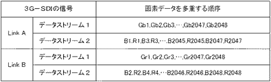
本実施例では、動画データをSDI規格に従って送信する。詳しくは、SMPTE ST 425(3G−SDI)のレベルBに準拠し、SMPTE ST 372(Dual Link)のR’G’B’+A 10ビットの多重化構造を適用して各画素データを配分する。また、画素のサンプルフォーマットは、SMPTE ST 2048−2で規定された、2048×1080/30Pに準拠する。 In this embodiment, moving image data is transmitted according to the SDI standard. More specifically, each pixel data is distributed by applying a 10-bit multiplexing structure of R'G'B '+ A of SMPTE ST 372 (Dual Link) in accordance with level B of SMPTE ST 425 (3G-SDI). The pixel sample format conforms to 2048 × 1080 / 30P defined by SMPTE ST 2048-2.
図8は、この規格に従って、有効映像期間(デジタルアクティブライン)に多重される画素データの各チャンネルへの配分構成を示している。この分配構成に従って制御部112は、データストリームを生成する各多重部に画素データを順番に供給する。例えば、多重部305は、画素データをGb(1)、Gb(2)・・Gb(2048)をこの順番で受け取り、Link Aのデータストリーム1を生成していく。
FIG. 8 shows a distribution configuration of pixel data multiplexed in an effective video period (digital active line) according to this standard to each channel. In accordance with this distribution configuration, the
制御部112は、同様の配分方法で、メモリ303に記録された八つのエリアの周辺画素データをFIFO701に供給する。供給するタイミングは、図6で設定した多重位置(サンプル位置)に従い算出される。
The
ライン計算部702は、撮像装置100から出力された動画データを受信する受信装置に対して、映像信号の区切り位置を認識するための識別子SAV/EAVを生成する。また、ライン番号の管理用のデータLN(Line Number)および伝送エラーチェック用のデータCRCC(Cyclic Redundancy Check Code)を生成する。タイミング制御部703は、制御部112から画素データを読み出すタイミングを制御する読出しクロックと、有効映像期間(デジタルアクティブライン)や垂直/水平ブランキング領域の期間のタイミング情報を受信する。有効映像期間のタイミング情報は、データストリームの信号に有効画素のデータを多重させる期間である。また、ブランキング領域の期間のタイミング情報は、周辺画素データを多重させる期間である。各エリアの周辺画素データを多重するタイミング情報は、制御部112により図6のデータテーブルの情報から算出される。そして、タイミング制御部703は、画素データを多重するタイミングパルスを発生する。
The
切り替え制御部704は、切り替え部706を制御して、FIFO701及びライン計算部702からの出力の一方を選択してRAM705に出力する。切り替え制御704は、供給されたタイミングパルスに基づいて、FIFO701から画素データを読み出すタイミングを切り替える。そして、読出しタイミングを切り替えながら、生成中のデータストリームに画素データを多重したり、SAV/EAV,LN,CRCCを多重したりする。
The switching
以上の動作により、多重部305から308は、それぞれのRAM705に、データストリームを記憶する(第一のデータ多重手段)。図9は、図5で示した各画素プレーンにおける1ラインの画素データを、この1ライン分に相当する4本のデータストリームに多重した結果を示す(多重した周辺画素データは省略する)。例えば、Gb3の“3”の番号は、Gbの画素プレーンの左端の画素データからの順番に対応する。
Through the above operation, the multiplexing
ここでは、RAWフレームを構成する2ラインに配置されたR、Gr、Gb、Bの画素データが、それぞれ1ライン分のデータストリームに多重されることを示している。 Here, R, Gr, Gb, and B pixel data arranged in two lines constituting the RAW frame are each multiplexed into a data stream for one line.
図10は、各多重部が生成する1枚のRAWフレームに対応するデータストリームのデータ構成を示す。周辺画素データは、図6のデータテーブルの多重位置の情報に従ってサンプル位置(同図中のサンプル番号)が特定され、水平および垂直ブランキング領域に多重される。 FIG. 10 shows a data structure of a data stream corresponding to one RAW frame generated by each multiplexing unit. In the peripheral pixel data, the sample position (sample number in the figure) is specified according to the information on the multiplexing position in the data table of FIG. 6, and multiplexed in the horizontal and vertical blanking areas.
図3において、アンシラリー多重部309は、多重部305から308により供給されたデータストリームにタイムコード、ペイロードID、そして図6のデータテーブルの情報などを多重する。多重方法は、SMPTE291に準拠する。
In FIG. 3, an
アンシラリー多重部309は、メモリ114より読み出したデータテーブルの情報を、図11で示すType2のアンシラリーパケット(ANCパケット)の各10ビットで構成されるユーザーデータワード(User Data Words)領域に格納する。格納するデータの形式は、それぞれの情報が値として取得できるものであれば、どのような形式であってもよい。また、ANCパケットの種類はヘッダ情報であるDID(Data IDentifier)とSDID(Secondary Data IDentifier)で識別される。これらには、本実施例で定義するデータテーブルに関する情報(メタ情報)であることを示す所定の値を設定する。
The
アンシラリー多重部309は、一例として、Link Aのデータストリーム1のライン番号6で指定される水平ブランキング領域にこのANCデータパケットを多重する(第二のデータ多重手段)。図12は、上記ANCパケットを多重したデータストリームのデータ構成を示す。
As an example, the
マルチプレクサ110は、アンシラリー多重部309により各種ANCパケットが多重された4本のデータストリームをSMPTE ST 425に準拠してワード単位で交互に多重化して単一のデータストリームとし、3G−SDIの信号として外部に送信する。
The
なお、本実施例では、周辺画素データを多重した位置を特定する情報として、SDIの信号に多重するライン番号、サンプル番号、ライン数、サンプル数の情報を設定した。しかし、この多重位置を特定する情報として、例えば、カメラの型番(タイプ)と動作モードの組み合わせなどにより一意的に多重位置が特定できる、IDの情報を利用する方法もある。 In the present embodiment, information on the line number, sample number, number of lines, and number of samples to be multiplexed on the SDI signal is set as information for specifying the position where the peripheral pixel data is multiplexed. However, as information for specifying the multiple position, there is also a method of using ID information in which the multiple position can be uniquely specified by, for example, a combination of a camera model number (type) and an operation mode.
SDIの信号では、有効画素以外の情報を多重する場合、その情報をANCパケットに格納してブランキング領域に重畳する。本実施例のように有効画素の上方と下方に位置する周辺画素のデータは、数ライン分の多重領域を要する。この周辺画素データは、仮にANCパケットのユーザーデータワード(255ワード)に格納する方法である場合、255ワードの制限があることから、複数パケットに分割して信号に多重することになる。この際、ANCパケットはヘッダの箇所が冗長となり、多重領域をより多く消費してしまう。このような問題を解消するために、周辺画素のデータをSDIのデータストリームのブランキング領域に多重するとき、デジタルアクティブラインへの画素データの多重方法と同一の方法を適用した。これは、SDIの信号上の領域に、周辺画素データを効率的に多重する方法である。 In the SDI signal, when information other than effective pixels is multiplexed, the information is stored in an ANC packet and superimposed on the blanking area. As in this embodiment, the data of the peripheral pixels located above and below the effective pixels requires multiple lines for several lines. If this peripheral pixel data is stored in the user data word (255 words) of the ANC packet, there is a limit of 255 words, so that it is divided into a plurality of packets and multiplexed into a signal. At this time, the header portion of the ANC packet becomes redundant, and more multiplex areas are consumed. In order to solve such a problem, the same method as the method of multiplexing pixel data on the digital active line is applied when the data of peripheral pixels is multiplexed in the blanking region of the SDI data stream. This is a method of efficiently multiplexing peripheral pixel data in an area on an SDI signal.
また、上記のように、多重した周辺画素データであっても、それを多重した位置に関する情報と元のRAWフレームにおけるその周辺画素データの位置情報とをANCパケットに格納して送信している。これにより、受信側はそのパケットを、SMPTE 291に準拠した標準の方法に従うことで、正確に受信することが可能になる。
受信装置は、ANCパケットを解析すれば、有効画素の周辺画素データが伝送信号上で多重されている位置を特定して取り出すことができる。
In addition, as described above, even with respect to multiplexed peripheral pixel data, information related to the multiplexed position and the positional information of the peripheral pixel data in the original RAW frame are stored in the ANC packet and transmitted. As a result, the receiving side can accurately receive the packet by following a standard method based on SMPTE 291.
By analyzing the ANC packet, the receiving apparatus can identify and extract the position where the peripheral pixel data of the effective pixel is multiplexed on the transmission signal.
本実施例では、ベイヤー構造で構成された画素配列4096×2048の有効画素のデータと、周辺画素のデータを伝送した。この画素データは、後工程のワークフローにおいて、ベイヤー構造のRAWフレームの配列に再構成された後、ディベイヤー処理が施されることによって、RGBの信号から構成される画像データに変換することができる。
In this embodiment, the effective pixel data of the
そして、このディベイヤー処理を行うとき、4096×2048の有効画素の左右上下に位置する端領域を正しく現像するために、本実施例で伝送した周辺画素データを利用することができる。 When this debayer processing is performed, the peripheral pixel data transmitted in the present embodiment can be used in order to correctly develop the end regions located on the left, right, top and bottom of the effective pixels of 4096 × 2048.
このように、本発明によれば、ベイヤー構造の画素配列で得られた動画フレームデータの伝送処理工程において、フレーム端の領域の補間処理で不足する画素の情報を伝送信号の所定の位置に多重している。これにより、送信先での受信した画像データの変換処理を正確に行うことが可能となる。 As described above, according to the present invention, in the moving image frame data transmission processing step obtained with the Bayer-structured pixel array, the pixel information that is insufficient in the interpolation processing of the frame end region is multiplexed at a predetermined position of the transmission signal. doing. This makes it possible to accurately convert the received image data at the transmission destination.
なお、本発明の画像処理構成は、上述した撮像装置だけでなく、PC等のデータ処理機能と伝送機能を有する装置にも適用することが可能である。また、本発明のデータ処理のみを他の装置で行い、処理したデータをPC等の通信機能を有する装置に供給して送信する場合の他の装置にも適用できるのは言うまでもない。 Note that the image processing configuration of the present invention can be applied not only to the imaging apparatus described above but also to an apparatus having a data processing function and a transmission function such as a PC. Further, it goes without saying that the present invention can also be applied to other devices in which only the data processing of the present invention is performed by another device and the processed data is supplied to a device such as a PC and transmitted.
また、上述した実施形態において、図3、6〜9、及び11に示す画像データの伝送データの生成構成は、当該構成に含まれる各機能を実現する為のプログラムをメモリ113から読み出し、制御部112のCPUがそれを実行することでも実現できる。
In the above-described embodiment, the image data transmission data generation configuration illustrated in FIGS. 3, 6 to 9, and 11 is read from the
その場合、図3、6〜9、及び11が示す構成に係わる各処理の全部または一部の機能を専用のハードウェアにより実現してもよい。また、上述したメモリは、フラッシュメモリ等の不揮発性のメモリに限らず、光磁気ディスク装置、CD−ROM等の読み出しのみが可能な記録媒体、RAM以外の揮発性のメモリとすることが可能である。また、それらの組合せによるコンピュータ読み取り、書き込み可能な記録媒体により構成してもよい。 In that case, all or some of the functions of the processes related to the configuration shown in FIGS. 3, 6 to 9 and 11 may be realized by dedicated hardware. The above-described memory is not limited to a non-volatile memory such as a flash memory, but may be a magneto-optical disk device, a recording medium such as a CD-ROM, or a volatile memory other than a RAM. is there. Moreover, you may comprise by the computer-readable / writable recording medium by those combination.
また、本発明の伝送データの生成処理の機能を実現する為のプログラムをコンピュータ読み取り可能な記録媒体に記録し、この記録媒体に記録されたプログラムをコンピュータシステムに読み込ませて実行させることにより各処理を実現しても良い。なお、ここでいう「コンピュータシステム」とは、OSや周辺機器等のハードウェアを含むものとする。具体的には、記憶媒体から読み出されたプログラムが、コンピュータに挿入された機能拡張ボードやコンピュータに接続された機能拡張ユニットに備わるメモリに書きこまれる。その後、そのプログラムの指示に基づき、その機能拡張ボードや機能拡張ユニットに備わるCPUなどが実際の処理の一部または全部を行い、その処理によって前述した実施形態の機能が実現される場合も含む。 In addition, a program for realizing the transmission data generation processing function of the present invention is recorded on a computer-readable recording medium, and the program recorded on the recording medium is read into a computer system and executed to execute each processing. May be realized. Here, the “computer system” includes an OS and hardware such as peripheral devices. Specifically, the program read from the storage medium is written into a memory provided in a function expansion board inserted into the computer or a function expansion unit connected to the computer. After that, the CPU of the function expansion board or function expansion unit performs part or all of the actual processing based on the instructions of the program, and the functions of the above-described embodiments are realized by the processing.
また、「コンピュータ読み取り可能な記録媒体」とは、フレキシブルディスク、光磁気ディスク、ROM、CD−ROM等の可搬媒体、コンピュータシステムに内蔵されるハードディスク等の記憶装置のことをいう。さらに「コンピュータ読み取り可能な記録媒体」とは、一定時間プログラムを保持しているものも含むものとする。例えば、インターネット等のネットワークや電話回線等の通信回線を介してプログラムが送信された場合のサーバやクライアントとなるコンピュータシステム内部の揮発メモリ(RAM)等を含む。 The “computer-readable recording medium” refers to a storage device such as a flexible medium, a magneto-optical disk, a portable medium such as a ROM and a CD-ROM, and a hard disk incorporated in a computer system. Furthermore, the “computer-readable recording medium” includes a medium that holds a program for a certain period of time. For example, it includes a volatile memory (RAM) inside a computer system that becomes a server or client when a program is transmitted via a network such as the Internet or a communication line such as a telephone line.
また、上記プログラムは、このプログラムを記憶装置等に格納したコンピュータシステムから、伝送媒体を介して、あるいは、伝送媒体中の伝送波により他のコンピュータシステムに伝送されてもよい。ここで、プログラムを伝送する「伝送媒体」は、インターネット等のネットワーク(通信網)や電話回線等の通信回線(通信線)のように情報を伝送する機能を有する媒体のことをいう。 The program may be transmitted from a computer system storing the program in a storage device or the like to another computer system via a transmission medium or by a transmission wave in the transmission medium. Here, the “transmission medium” for transmitting the program refers to a medium having a function of transmitting information, such as a network (communication network) such as the Internet or a communication line (communication line) such as a telephone line.
また、上記プログラムは、前述した機能の一部を実現する為のものであっても良い。さらに、前述した機能をコンピュータシステムに既に記録されているプログラムとの組合せで実現できるもの、いわゆる差分ファイル(差分プログラム)であっても良い。 The program may be for realizing a part of the functions described above. Furthermore, what can implement | achieve the function mentioned above in combination with the program already recorded on the computer system, and what is called a difference file (difference program) may be sufficient.
また、上記のプログラムを記録したコンピュータ読み取り可能な記録媒体等のプログラムプロダクトも本発明の実施形態として適用することができる。上記のプログラム、記録媒体、伝送媒体およびプログラムプロダクトは、本発明の範疇に含まれる。 A program product such as a computer-readable recording medium in which the above program is recorded can also be applied as an embodiment of the present invention. The above program, recording medium, transmission medium, and program product are included in the scope of the present invention.
以上、この発明の実施形態について図面を参照して詳述してきたが、具体的な構成はこの実施形態に限られるものではなく、この発明の要旨を逸脱しない範囲の設計等も含まれる。 The embodiment of the present invention has been described in detail with reference to the drawings. However, the specific configuration is not limited to this embodiment, and includes designs and the like that do not depart from the gist of the present invention.
Claims (13)
前記動画データの有効画素領域の画像データを送信するための送信方式に従い、前記取得手段により取得された前記動画データから前記有効画素領域の画像データを含むデータストリームを生成する手段であって、前記有効画素領域の画像データに対し、前記有効画素領域の周辺の画素領域の画像データと、前記周辺の画素領域の画像データが多重されている位置に関する位置情報と、を多重することにより、前記データストリームを生成する生成手段と、
前記生成手段により生成された前記データストリームを送信する送信手段とを備えることを特徴とする画像処理装置。 An acquisition means for acquiring video data;
Means for generating a data stream including image data of the effective pixel region from the moving image data acquired by the acquisition unit, according to a transmission method for transmitting image data of the effective pixel region of the moving image data; The image data of the effective pixel region is multiplexed with the image data of the pixel region around the effective pixel region and the position information related to the position where the image data of the peripheral pixel region is multiplexed. Generating means for generating a stream;
An image processing apparatus comprising: a transmission unit that transmits the data stream generated by the generation unit.
前記動画データの有効画素領域の画像データを送信するための送信方式に従い、前記動画データを取得するステップにより取得された前記動画データから前記有効画素領域の画像データを含むデータストリームを生成するステップであって、前記有効画素領域の画像データに対し、前記有効画素領域の周辺の画素領域の画像データと、前記周辺の画素領域の画像データが多重されている位置に関する位置情報と、を多重することにより、前記データストリームを生成するステップと、
前記データストリームを生成するステップにより生成された前記データストリームを送信するステップとを備えることを特徴とする画像処理方法。 Acquiring video data;
A step of generating a data stream including image data of the effective pixel region from the moving image data acquired by the step of acquiring the moving image data according to a transmission method for transmitting image data of the effective pixel region of the moving image data; The image data of the effective pixel region is multiplexed with the image data of the pixel region around the effective pixel region and the position information regarding the position where the image data of the peripheral pixel region is multiplexed. Generating the data stream;
Image processing method characterized by comprising the step of transmitting the data stream generated by the step of generating the data stream.
Priority Applications (2)
| Application Number | Priority Date | Filing Date | Title |
|---|---|---|---|
| JP2012079529A JP5973766B2 (en) | 2012-03-30 | 2012-03-30 | Image processing device |
| US13/849,063 US8970783B2 (en) | 2012-03-30 | 2013-03-22 | Image processing apparatus and control method therefor |
Applications Claiming Priority (1)
| Application Number | Priority Date | Filing Date | Title |
|---|---|---|---|
| JP2012079529A JP5973766B2 (en) | 2012-03-30 | 2012-03-30 | Image processing device |
Publications (3)
| Publication Number | Publication Date |
|---|---|
| JP2013211644A JP2013211644A (en) | 2013-10-10 |
| JP2013211644A5 JP2013211644A5 (en) | 2015-05-07 |
| JP5973766B2 true JP5973766B2 (en) | 2016-08-23 |
Family
ID=49234498
Family Applications (1)
| Application Number | Title | Priority Date | Filing Date |
|---|---|---|---|
| JP2012079529A Active JP5973766B2 (en) | 2012-03-30 | 2012-03-30 | Image processing device |
Country Status (2)
| Country | Link |
|---|---|
| US (1) | US8970783B2 (en) |
| JP (1) | JP5973766B2 (en) |
Families Citing this family (2)
| Publication number | Priority date | Publication date | Assignee | Title |
|---|---|---|---|---|
| US9807336B2 (en) * | 2014-11-12 | 2017-10-31 | Mediatek Inc. | Dynamic adjustment of video frame sampling rate |
| JP6953244B2 (en) | 2017-09-07 | 2021-10-27 | キヤノン株式会社 | Image transmission device and its control method |
Family Cites Families (21)
| Publication number | Priority date | Publication date | Assignee | Title |
|---|---|---|---|---|
| JP2002199414A (en) | 2000-12-26 | 2002-07-12 | Canon Inc | Imaging device and imaging method |
| JP2002330439A (en) * | 2001-04-27 | 2002-11-15 | Matsushita Electric Ind Co Ltd | Transmitter for image information, transmission system for the image information and transmission method for the image information |
| DE10300048B4 (en) * | 2002-01-05 | 2005-05-12 | Samsung Electronics Co., Ltd., Suwon | Image coding method for motion picture expert groups, involves image quantizing data in accordance with quantization parameter, and coding entropy of quantized image data using entropy coding unit |
| JP4114658B2 (en) * | 2004-04-13 | 2008-07-09 | ソニー株式会社 | Data transmitting apparatus and data receiving apparatus |
| JP4264655B2 (en) * | 2005-03-17 | 2009-05-20 | ソニー株式会社 | Video recording system, video recording apparatus, and video signal recording method |
| EP2131583A1 (en) * | 2007-03-29 | 2009-12-09 | Sharp Kabushiki Kaisha | Video transmitter, video receiver, video recorder, video reproducer, and video display |
| JP4623069B2 (en) * | 2007-09-14 | 2011-02-02 | ソニー株式会社 | Information processing apparatus and method, program, and recording medium |
| JP4645638B2 (en) * | 2007-11-22 | 2011-03-09 | ソニー株式会社 | Signal transmitting apparatus, signal transmitting method, signal receiving apparatus, and signal receiving method |
| JP5109697B2 (en) * | 2008-02-07 | 2012-12-26 | ソニー株式会社 | Image transmission device, image reception device, image transmission / reception system, image transmission program, and image reception program |
| JP5414797B2 (en) * | 2008-12-25 | 2014-02-12 | ジーブイビービー ホールディングス エス.エイ.アール.エル. | Transmitting apparatus, receiving apparatus, system, and method used therein |
| JP5271243B2 (en) * | 2009-12-07 | 2013-08-21 | 日本放送協会 | Image feature information multiplexing device, interpolation video generation device, receiver, image feature information multiplexing program, and interpolation video generation program |
| JP5640371B2 (en) * | 2009-12-18 | 2014-12-17 | ソニー株式会社 | Camera system and image processing method |
| CN102131119A (en) * | 2010-01-14 | 2011-07-20 | 索尼公司 | Information processing apparatus, information processing method, and program |
| JP5454215B2 (en) * | 2010-02-22 | 2014-03-26 | ソニー株式会社 | Transmission device, transmission method, reception device, reception method, and signal transmission system |
| US8698885B2 (en) * | 2011-02-14 | 2014-04-15 | Intuitive Surgical Operations, Inc. | Methods and apparatus for demosaicing images with highly correlated color channels |
| JP2012248984A (en) * | 2011-05-26 | 2012-12-13 | Sony Corp | Signal transmitter, signal transmission method, signal receiver, signal reception method and signal transmission system |
| JP5414752B2 (en) * | 2011-08-08 | 2014-02-12 | キヤノン株式会社 | Image processing method, image processing apparatus, imaging apparatus, and image processing program |
| JP5760953B2 (en) * | 2011-10-31 | 2015-08-12 | 富士通株式会社 | Moving picture decoding apparatus, moving picture encoding apparatus, moving picture decoding method, and moving picture encoding method |
| MX2013008943A (en) * | 2011-11-07 | 2013-09-06 | Panasonic Corp | Image encoding method, image decoding method, image encoding device, image decoding device, and image encoding/decoding device. |
| JP6032919B2 (en) * | 2012-03-30 | 2016-11-30 | キヤノン株式会社 | Image processing device |
| JP2013219544A (en) * | 2012-04-09 | 2013-10-24 | Ricoh Co Ltd | Image processing apparatus, image processing method, and image processing program |
-
2012
- 2012-03-30 JP JP2012079529A patent/JP5973766B2/en active Active
-
2013
- 2013-03-22 US US13/849,063 patent/US8970783B2/en not_active Expired - Fee Related
Also Published As
| Publication number | Publication date |
|---|---|
| US8970783B2 (en) | 2015-03-03 |
| JP2013211644A (en) | 2013-10-10 |
| US20130258163A1 (en) | 2013-10-03 |
Similar Documents
| Publication | Publication Date | Title |
|---|---|---|
| JP6032919B2 (en) | Image processing device | |
| US20110261215A1 (en) | Image processing apparatus and method of controlling the same | |
| JP2009010821A (en) | Imaging device and imaging method, recording medium, and program | |
| JP2019114914A (en) | Imaging apparatus, control method of the same, program, and imaging system | |
| JP2008005436A (en) | Imaging apparatus and control method thereof, information processor, printer, and print data generating method | |
| US9445085B2 (en) | Imaging apparatus, method for controlling imaging apparatus, and system therefor | |
| JP2007150439A (en) | Imaging apparatus, imaging method, and program | |
| US20160343403A1 (en) | Moving image generating apparatus, moving image generating method and storage medium | |
| EP1763224B1 (en) | Video signal processing in a camera control unit | |
| JP2020178292A5 (en) | Communication equipment and its control method, program | |
| JP6351212B2 (en) | IMAGING DEVICE, IMAGING DEVICE CONTROL METHOD AND SYSTEM | |
| JP5936323B2 (en) | Image recording apparatus and control method thereof | |
| JP5973766B2 (en) | Image processing device | |
| US20130177287A1 (en) | Reproduction apparatus, image capturing apparatus, and program | |
| JP2010187113A (en) | Imaging apparatus, and white balance bracketing photographing program | |
| JP6548500B2 (en) | File name conversion apparatus, method, program, and recording system | |
| JP2009182754A (en) | Image processor | |
| JP6351213B2 (en) | IMAGING DEVICE, IMAGING DEVICE CONTROL METHOD AND SYSTEM | |
| JP6594485B2 (en) | IMAGING DEVICE, IMAGING DEVICE CONTROL METHOD AND SYSTEM | |
| JP6602425B2 (en) | IMAGING DEVICE, IMAGING DEVICE CONTROL METHOD AND SYSTEM | |
| JP2006094192A (en) | Imaging device | |
| JP2007074371A (en) | Photographing device, display device, and photographing display system | |
| JP2014049882A (en) | Imaging apparatus | |
| JP2018182622A (en) | Imaging apparatus, and control method, program and recording medium thereof | |
| JP2010239267A (en) | Imaging apparatus, method for controlling peripheral darkening correction, and program |
Legal Events
| Date | Code | Title | Description |
|---|---|---|---|
| RD05 | Notification of revocation of power of attorney |
Free format text: JAPANESE INTERMEDIATE CODE: A7425 Effective date: 20130701 |
|
| A521 | Request for written amendment filed |
Free format text: JAPANESE INTERMEDIATE CODE: A523 Effective date: 20150324 |
|
| A621 | Written request for application examination |
Free format text: JAPANESE INTERMEDIATE CODE: A621 Effective date: 20150324 |
|
| A977 | Report on retrieval |
Free format text: JAPANESE INTERMEDIATE CODE: A971007 Effective date: 20151224 |
|
| A131 | Notification of reasons for refusal |
Free format text: JAPANESE INTERMEDIATE CODE: A131 Effective date: 20160107 |
|
| A521 | Request for written amendment filed |
Free format text: JAPANESE INTERMEDIATE CODE: A523 Effective date: 20160302 |
|
| TRDD | Decision of grant or rejection written | ||
| A01 | Written decision to grant a patent or to grant a registration (utility model) |
Free format text: JAPANESE INTERMEDIATE CODE: A01 Effective date: 20160616 |
|
| A61 | First payment of annual fees (during grant procedure) |
Free format text: JAPANESE INTERMEDIATE CODE: A61 Effective date: 20160715 |
|
| R151 | Written notification of patent or utility model registration |
Ref document number: 5973766 Country of ref document: JP Free format text: JAPANESE INTERMEDIATE CODE: R151 |