JP5968152B2 - Switching power supply and image forming apparatus - Google Patents
Switching power supply and image forming apparatus Download PDFInfo
- Publication number
- JP5968152B2 JP5968152B2 JP2012173755A JP2012173755A JP5968152B2 JP 5968152 B2 JP5968152 B2 JP 5968152B2 JP 2012173755 A JP2012173755 A JP 2012173755A JP 2012173755 A JP2012173755 A JP 2012173755A JP 5968152 B2 JP5968152 B2 JP 5968152B2
- Authority
- JP
- Japan
- Prior art keywords
- voltage
- transformer
- switching
- unit
- switching unit
- Prior art date
- Legal status (The legal status is an assumption and is not a legal conclusion. Google has not performed a legal analysis and makes no representation as to the accuracy of the status listed.)
- Active
Links
Images


Classifications
-
- H—ELECTRICITY
- H02—GENERATION; CONVERSION OR DISTRIBUTION OF ELECTRIC POWER
- H02M—APPARATUS FOR CONVERSION BETWEEN AC AND AC, BETWEEN AC AND DC, OR BETWEEN DC AND DC, AND FOR USE WITH MAINS OR SIMILAR POWER SUPPLY SYSTEMS; CONVERSION OF DC OR AC INPUT POWER INTO SURGE OUTPUT POWER; CONTROL OR REGULATION THEREOF
- H02M3/00—Conversion of dc power input into dc power output
- H02M3/22—Conversion of dc power input into dc power output with intermediate conversion into ac
- H02M3/24—Conversion of dc power input into dc power output with intermediate conversion into ac by static converters
- H02M3/28—Conversion of dc power input into dc power output with intermediate conversion into ac by static converters using discharge tubes with control electrode or semiconductor devices with control electrode to produce the intermediate ac
- H02M3/325—Conversion of dc power input into dc power output with intermediate conversion into ac by static converters using discharge tubes with control electrode or semiconductor devices with control electrode to produce the intermediate ac using devices of a triode or a transistor type requiring continuous application of a control signal
- H02M3/335—Conversion of dc power input into dc power output with intermediate conversion into ac by static converters using discharge tubes with control electrode or semiconductor devices with control electrode to produce the intermediate ac using devices of a triode or a transistor type requiring continuous application of a control signal using semiconductor devices only
-
- G—PHYSICS
- G03—PHOTOGRAPHY; CINEMATOGRAPHY; ANALOGOUS TECHNIQUES USING WAVES OTHER THAN OPTICAL WAVES; ELECTROGRAPHY; HOLOGRAPHY
- G03G—ELECTROGRAPHY; ELECTROPHOTOGRAPHY; MAGNETOGRAPHY
- G03G21/00—Arrangements not provided for by groups G03G13/00 - G03G19/00, e.g. cleaning, elimination of residual charge
-
- H—ELECTRICITY
- H02—GENERATION; CONVERSION OR DISTRIBUTION OF ELECTRIC POWER
- H02M—APPARATUS FOR CONVERSION BETWEEN AC AND AC, BETWEEN AC AND DC, OR BETWEEN DC AND DC, AND FOR USE WITH MAINS OR SIMILAR POWER SUPPLY SYSTEMS; CONVERSION OF DC OR AC INPUT POWER INTO SURGE OUTPUT POWER; CONTROL OR REGULATION THEREOF
- H02M3/00—Conversion of dc power input into dc power output
- H02M3/22—Conversion of dc power input into dc power output with intermediate conversion into ac
- H02M3/24—Conversion of dc power input into dc power output with intermediate conversion into ac by static converters
- H02M3/28—Conversion of dc power input into dc power output with intermediate conversion into ac by static converters using discharge tubes with control electrode or semiconductor devices with control electrode to produce the intermediate ac
- H02M3/325—Conversion of dc power input into dc power output with intermediate conversion into ac by static converters using discharge tubes with control electrode or semiconductor devices with control electrode to produce the intermediate ac using devices of a triode or a transistor type requiring continuous application of a control signal
- H02M3/335—Conversion of dc power input into dc power output with intermediate conversion into ac by static converters using discharge tubes with control electrode or semiconductor devices with control electrode to produce the intermediate ac using devices of a triode or a transistor type requiring continuous application of a control signal using semiconductor devices only
- H02M3/33507—Conversion of dc power input into dc power output with intermediate conversion into ac by static converters using discharge tubes with control electrode or semiconductor devices with control electrode to produce the intermediate ac using devices of a triode or a transistor type requiring continuous application of a control signal using semiconductor devices only with automatic control of the output voltage or current, e.g. flyback converters
- H02M3/33523—Conversion of dc power input into dc power output with intermediate conversion into ac by static converters using discharge tubes with control electrode or semiconductor devices with control electrode to produce the intermediate ac using devices of a triode or a transistor type requiring continuous application of a control signal using semiconductor devices only with automatic control of the output voltage or current, e.g. flyback converters with galvanic isolation between input and output of both the power stage and the feedback loop
-
- H—ELECTRICITY
- H02—GENERATION; CONVERSION OR DISTRIBUTION OF ELECTRIC POWER
- H02M—APPARATUS FOR CONVERSION BETWEEN AC AND AC, BETWEEN AC AND DC, OR BETWEEN DC AND DC, AND FOR USE WITH MAINS OR SIMILAR POWER SUPPLY SYSTEMS; CONVERSION OF DC OR AC INPUT POWER INTO SURGE OUTPUT POWER; CONTROL OR REGULATION THEREOF
- H02M1/00—Details of apparatus for conversion
- H02M1/0003—Details of control, feedback or regulation circuits
- H02M1/0032—Control circuits allowing low power mode operation, e.g. in standby mode
- H02M1/0035—Control circuits allowing low power mode operation, e.g. in standby mode using burst mode control
-
- H—ELECTRICITY
- H02—GENERATION; CONVERSION OR DISTRIBUTION OF ELECTRIC POWER
- H02M—APPARATUS FOR CONVERSION BETWEEN AC AND AC, BETWEEN AC AND DC, OR BETWEEN DC AND DC, AND FOR USE WITH MAINS OR SIMILAR POWER SUPPLY SYSTEMS; CONVERSION OF DC OR AC INPUT POWER INTO SURGE OUTPUT POWER; CONTROL OR REGULATION THEREOF
- H02M1/00—Details of apparatus for conversion
- H02M1/0048—Circuits or arrangements for reducing losses
- H02M1/0054—Transistor switching losses
-
- Y—GENERAL TAGGING OF NEW TECHNOLOGICAL DEVELOPMENTS; GENERAL TAGGING OF CROSS-SECTIONAL TECHNOLOGIES SPANNING OVER SEVERAL SECTIONS OF THE IPC; TECHNICAL SUBJECTS COVERED BY FORMER USPC CROSS-REFERENCE ART COLLECTIONS [XRACs] AND DIGESTS
- Y02—TECHNOLOGIES OR APPLICATIONS FOR MITIGATION OR ADAPTATION AGAINST CLIMATE CHANGE
- Y02B—CLIMATE CHANGE MITIGATION TECHNOLOGIES RELATED TO BUILDINGS, e.g. HOUSING, HOUSE APPLIANCES OR RELATED END-USER APPLICATIONS
- Y02B70/00—Technologies for an efficient end-user side electric power management and consumption
- Y02B70/10—Technologies improving the efficiency by using switched-mode power supplies [SMPS], i.e. efficient power electronics conversion e.g. power factor correction or reduction of losses in power supplies or efficient standby modes
Landscapes
- Engineering & Computer Science (AREA)
- Power Engineering (AREA)
- Physics & Mathematics (AREA)
- General Physics & Mathematics (AREA)
- Dc-Dc Converters (AREA)
- Control Or Security For Electrophotography (AREA)
Description
本発明は、直流電圧を生成するスイッチング電源に関する。 The present invention relates to a switching power supply that generates a DC voltage.
近年、様々な電子機器において、消費電力をより低減して省電力化した機器が望まれており、電子機器に電力を供給する電源においても一層の省電力化が望まれている。電子機器の電源の一例であるスイッチング電源の構成概念図を図15に示す。図15において、商用交流電源100から入力される交流電圧を整流部140を介してトランス104に入力し、FET等のスイッチング素子108を制御回路144から送出される信号に基づいて所定の周波数でスイッチング動作させ、トランス104の一次側を駆動する。そして、トランス104の二次側に発生した電圧を平滑部141により平滑することにより直流電圧Vを生成する。このように、所定の周波数でスイッチング素子108を駆動して、所望の直流電圧を生成するスイッチング電源が広く使用されている。このようなスイッチング電源では、例えば、電子機器が動作していな状態のような省電力動作時(軽負荷運転時ともいう)において、スイッチング素子108のスイッチング回数を減らして(スイッチング周波数を低下させて)動作効率を向上させるものがある。軽負荷運転時におけるスイッチング電源の損失の多くは、スイッチング動作による損失であり、この損失を低減させるために、スイッチング素子108がオンしている時間(オン時間ともいう)を長くして、1回当たりのスイッチング動作のエネルギーを大きくする。これにより、休止期間を長くして単位時間当たりのスイッチング回数を減らす工夫がなされている。しかし、休止期間を長くすると、スイッチング周波数がより低下し、スイッチング動作に伴ってトランスから発生する音が可聴域に入る可能性が出てくる。また、この音は、高調波成分を含むために耳障りな音になる。
In recent years, in various electronic devices, devices that reduce power consumption and save power have been desired, and further power savings have been desired for power supplies that supply power to electronic devices. FIG. 15 shows a conceptual diagram of a switching power supply as an example of a power supply for an electronic device. In FIG. 15, an AC voltage input from the commercial
以下、スイッチング周波数が高調波を含む音になる理由について説明する。スイッチング周波数が、数kHz以下になると、スイッチング素子の休止期間が長くなるため、トランス駆動電流波形は、図16に示すようなデルタ関数的な波形になる。ここで、図16は、スイッチング素子を1msec周期、オン時間5μsecの1波駆動パルスで、駆動した際のトランス駆動電流波形、及び、駆動パルス波形を示している。図16(a)はトランスの駆動電流波形であり、縦軸はトランス駆動電流(A)であり横軸は時間(sec)、図16(b)は駆動パルス波形であり、縦軸は駆動電圧(V)であり横軸は時間(sec)である。このようなトランス駆動電流波形に対して、周波数解析(高速フーリエ変換解析(FFT解析ともいう))を行った結果を図17に示す。 Hereinafter, the reason why the switching frequency becomes a sound including harmonics will be described. When the switching frequency becomes several kHz or less, the rest period of the switching element becomes longer, and the transformer drive current waveform becomes a delta function waveform as shown in FIG. Here, FIG. 16 shows a transformer drive current waveform and a drive pulse waveform when the switching element is driven with a 1-wave drive pulse having a 1 msec cycle and an ON time of 5 μsec. 16A shows the drive current waveform of the transformer, the vertical axis shows the transformer drive current (A), the horizontal axis shows time (sec), FIG. 16B shows the drive pulse waveform, and the vertical axis shows the drive voltage. (V) and the horizontal axis is time (sec). FIG. 17 shows the result of frequency analysis (fast Fourier transform analysis (also referred to as FFT analysis)) performed on such a transformer drive current waveform.
図17において、縦軸はトランス駆動電流(mA)、横軸は周波数(Hz)である。図17に示されるように、トランス駆動電流は、スイッチング周波数を基本波として、その逓倍周波数の高調波成分を持ち、この高調波成分で駆動されるエネルギーを有する電流波形になる。また、スイッチング電源のトランスもスイッチング動作して所定の共振周波数で駆動される。このトランスの機械的な共振周波数は、トランスのコア形状にも依存し、概ね、数kHz〜十数kHzの周波数帯域に共振周波数のピークを持つ。ここで、例えば、図16に示されるような、1波駆動パルスをスイッチング素子に与えて、機械的な共振周波数特性が18kHzをピークとして、18kHz周辺の周波数帯域に近い共振レベルを有するトランスを用いて駆動することを考える。この際に、トランスから発生する唸り音の音圧を図18に示す。図18において、縦軸はトランスの唸り音の音圧(dB)、横軸は周波数(Hz)であり、その音圧は、スイッチング周波数を基本波として、包絡線がトランスの機械的な共振周波数特性となるような高調波を含んだ特性になる。つまり、スイッチング周波数とトランスの機械的な共振周波数が重なり合うことにより、トランスの唸り音として可聴域に入る耳障りな音が発生する。 In FIG. 17, the vertical axis represents the transformer drive current (mA), and the horizontal axis represents the frequency (Hz). As shown in FIG. 17, the transformer drive current has a harmonic component of the multiplied frequency with the switching frequency as a fundamental wave, and has a current waveform having energy driven by this harmonic component. In addition, the transformer of the switching power supply also performs a switching operation and is driven at a predetermined resonance frequency. The mechanical resonance frequency of this transformer also depends on the core shape of the transformer, and generally has a resonance frequency peak in a frequency band of several kHz to several tens of kHz. Here, for example, a transformer having a resonance level close to a frequency band around 18 kHz with a mechanical resonance frequency characteristic peaking at 18 kHz is applied to the switching element as shown in FIG. Think about driving. At this time, the sound pressure of the roaring sound generated from the transformer is shown in FIG. In FIG. 18, the vertical axis represents the sound pressure (dB) of the roaring sound of the transformer, and the horizontal axis represents the frequency (Hz). The sound pressure is based on the switching frequency as the fundamental wave, and the envelope is the mechanical resonance frequency of the transformer. It becomes the characteristic including the harmonic that becomes the characteristic. That is, when the switching frequency and the mechanical resonance frequency of the transformer overlap, an unpleasant sound that enters the audible range is generated as a roaring sound of the transformer.
このようなトランスの唸り音の発生を低減する方法の1つとして、トランスの磁界の変化率を抑えて唸り音を低減させる方法が知られている。従来は、トランスの磁界の変化率を抑えるために、トランスのコア材に断面積の大きいものを用いたり、また、スイッチング素子のオン時間を短くしてトランスの1回当たりのスイッチング電流を小さくしたりする方法を採用していた。 As one method for reducing the occurrence of such a roaring sound of the transformer, a method of reducing the roaring sound by suppressing the rate of change of the magnetic field of the transformer is known. Conventionally, in order to reduce the rate of change of the magnetic field of the transformer, a transformer core material having a large cross-sectional area is used, or the switching element ON time is shortened to reduce the switching current per transformer. The method was used.
また、トランス駆動電流波形を工夫してトランスの唸り音の発生を低減する方法としては、スイッチング電源において、ソフトスタート回路を設けて、起動開始時にコンデンサ両端の電圧の立ち上げと立ち下げの際のデューティ比を徐々に変化させる方式がある。トランス駆動電流波形を徐々に大きく、また、徐々に小さくする電流波形にすれば、トランスの磁束変化を小さくできるため、唸り音の発生を低減することができる。なお、このような従来方式は、例えば、特許文献1や特許文献2に記載されている。
In addition, as a method of reducing the generation of transformer noise by devising the transformer drive current waveform, a soft start circuit is provided in the switching power supply, and the voltage at both ends of the capacitor is raised and lowered at the start of startup. There is a method of gradually changing the duty ratio. If the transformer drive current waveform is gradually increased and gradually reduced, the change in the magnetic flux of the transformer can be reduced, so that the generation of the roaring sound can be reduced. Such a conventional method is described in, for example,
しかし、トランスのコア材に断面積の大きいものを用いると、電源の小型化が困難になる。また、スイッチング素子のオン時間を短くする方法では、トランスの磁束変化を小さくすることにより、トランスの唸り音の発生は軽減されるものの、単位時間当たりのスイッチング回数を増やすことになり、スイッチング損失が増加する。また、トランス駆動電流波形を徐々に大きく、また、徐々に小さくするソフトスタートの電流波形にする方法では、軽負荷運転時において、更に消費電力を低減しようとする場合に、二次側負荷に供給するエネルギーが小さくなるため適用が困難になる。なぜなら、軽負荷運転時において、二次側への供給エネルギーがより小さくなると、ソフトスタート回路により徐々に電流波形を大きくする、また、小さくすることが困難であるからである。また、従来の方法では、1回当たりのスイッチング動作で供給するエネルギーを小さくして多くの回数スイッチングを行うか、もしくは、1回当たりのスイッチング動作で供給するエネルギーを変えずに二次側のコンデンサ容量を数倍に大きくする必要がある。前者の方法ではスイッチング損失が増加して効率を著しく損ねる。後者はコストアップになる。すなわち、スイッチング電源は、スイッチング回数を少なくしてスイッチング損失を低減したいが、その場合、1波当たりの駆動パルスによりトランスに与えられるエネルギーが大きくなるために、発生する音が大きくなるという矛盾を抱えている。 However, if a transformer having a large cross-sectional area is used, it is difficult to reduce the size of the power source. Also, in the method of shortening the on-time of the switching element, by reducing the change in the magnetic flux of the transformer, the generation of the roaring noise of the transformer is reduced, but the number of times of switching per unit time is increased and the switching loss is reduced. To increase. In addition, the soft drive current waveform that gradually increases and decreases the transformer drive current waveform is supplied to the secondary load when further reducing power consumption during light load operation. Application becomes difficult because of less energy. This is because it is difficult to gradually increase or decrease the current waveform by the soft start circuit if the energy supplied to the secondary side becomes smaller during light load operation. In the conventional method, the energy supplied in the switching operation per time is reduced and switching is performed many times, or the secondary side capacitor is not changed without changing the energy supplied in the switching operation per time. It is necessary to increase the capacity several times. In the former method, the switching loss increases and the efficiency is remarkably impaired. The latter increases costs. In other words, the switching power supply wants to reduce the switching loss by reducing the number of times of switching, but in that case, the energy given to the transformer by the drive pulse per wave increases, so there is a contradiction that the generated sound increases. ing.
本発明は上記の課題に鑑みてなされたものであり、スイッチング電源の軽負荷運転時において、トランスのサイズを大きくすることなく、かつ、スイッチング損失を増加させずに、トランスの唸り音の発生を低減することを目的する。 The present invention has been made in view of the above-described problems, and at the time of light load operation of a switching power supply, the generation of transformer roaring noise without increasing the size of the transformer and without increasing the switching loss. Aim to reduce.
本発明のスイッチング電源は、トランスと、前記トランスの一次側を駆動するスイッチング部と、前記トランスの二次側に発生する電圧を出力する出力部と、前記スイッチング部を連続的に駆動することにより前記出力部から第一電圧を出力する第一出力状態と、
前記スイッチング部を間欠的に駆動することにより前記出力部から前記第一電圧よりも小さい第二電圧を出力する第二出力状態と、を有し、前記第二出力状態において、前記スイッチング部が間欠的に駆動する際の駆動周期毎の前記スイッチング部のオン回数が周期的に変更されることを特徴とする。
The switching power supply of the present invention includes a transformer, a switching unit that drives a primary side of the transformer, an output unit that outputs a voltage generated on the secondary side of the transformer, and a continuous drive of the switching unit. A first output state for outputting a first voltage from the output unit;
A second output state that outputs a second voltage lower than the first voltage from the output unit by driving the switching unit intermittently, and the switching unit is intermittent in the second output state. turn on times of the switching unit of each drive cycle of the time of driving, characterized in Rukoto is periodically changed.
画像を形成するための画像形成部と、前記画像形成部の動作を制御する制御部と、前記制御部に電力を供給するスイッチング電源とを有し、前記電源は、トランスと、前記トランスの一次側を駆動するスイッチング部と、前記トランスの二次側に発生する電圧を出力する出力部と、前記スイッチング部を連続的に駆動することにより前記出力部から第一電圧を出力する第一の出力状態と、前記スイッチング部を間欠的に駆動することにより前記出力部から前記第一電圧よりも小さい第二電圧を出力する第二出力状態と、を有し、前記第二出力状態において、前記スイッチング部が間欠的に駆動する際の駆動周期毎の前記スイッチング部のオン回数が周期的に変更されることを特徴とする。 An image forming unit for forming an image; a control unit that controls an operation of the image forming unit; and a switching power source that supplies power to the control unit. The power source includes a transformer and a primary of the transformer A switching unit that drives a side, an output unit that outputs a voltage generated on the secondary side of the transformer, and a first output that outputs a first voltage from the output unit by continuously driving the switching unit A second output state in which a second voltage smaller than the first voltage is output from the output unit by intermittently driving the switching unit, and in the second output state, the switching part is the number of times of turning on the switching unit of each drive cycle when intermittently driven and wherein Rukoto is periodically changed.
以上説明したように、本発明によれば、スイッチング電源の軽負荷運転時において、トランスのサイズを大きくすることなく、かつ、スイッチング損失を増加させずに、トランスの唸り音の発生を低減することができる。 As described above, according to the present invention, during the light load operation of the switching power supply, it is possible to reduce the generation of the roaring noise of the transformer without increasing the size of the transformer and without increasing the switching loss. Can do.
以下に、本発明の構成及び動作について説明する。なお、以下に示す実施例は一例であって、この発明の技術的範囲をそれらのみに限定する趣旨のものではない。以下、添付図面を参照しながら、本発明を実施する為の形態を、実施例により詳しく説明する。 The configuration and operation of the present invention will be described below. In addition, the Example shown below is an example, Comprising: It is not the meaning which limits the technical scope of this invention only to them. Hereinafter, embodiments for carrying out the present invention will be described in detail with reference to the accompanying drawings.
(実施例1)
まず、実施例1について図1乃至図11を用いて説明する。なお、図において、上記従来例の説明図と同一構成及び機能に対応する部分については同一符号を付して説明を省略する。
Example 1
First, Example 1 will be described with reference to FIGS. In the figure, portions corresponding to the same configurations and functions as those in the above-described conventional example are denoted by the same reference numerals, and description thereof is omitted.
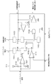
図1は、本実施例のスイッチング電源の構成概念を示している。図1の特徴は、商用交流電源100からの交流電圧から直流電圧Vを生成するスイッチング電源を、整流部140、スイッチング素子108で駆動されるトランス104、平滑部141、負荷状態判断部142及びパルス群生成部143から構成することである。負荷状態判断部142が、スイッチング電源が軽負荷運転状態であると判断した場合、パルス群生成部143は、スイッチング素子108のスイッチング動作を、休止期間を含んだ所定の周期(T1,T2,T3・・・)で行う(この動作はバースト動作ともいう)。そして、駆動パルス群中のパルス数を、所定の波数(n1,n2,n3・・・)のように可変する。このようなスイッチング動作によって、広範囲の周波数帯域に対して、トランス駆動電流波形のFFTスペクトラムのレベルを低減させる。これにより、トランスのサイズを大きくせずに、かつ、スイッチング損失を増加させずに、トランスの唸り音の発生を低減することができる。
FIG. 1 shows the configuration concept of the switching power supply of this embodiment. 1 is characterized in that a switching power source that generates a DC voltage V from an AC voltage from a commercial
まず、本実施例のスイッチング電源の詳細構成を説明する。図2に本実施例のスイッチング電源の構成を示す。なお、本実施例で例示するスイッチング電源は、擬似共振方式のスイッチング電源である。図2において、100は商用交流電源、101はダイオードブリッジ、102は一次電解コンデンサ、103は起動抵抗、104はトランス、105はトランスの一次巻線、106はトランスの二次巻線、107はトランスの補助巻線である。また、108はFETであり、トランス104への電源供給をオンオフするメインのスイッチング素子である。また、109は電流検出抵抗、110はスイッチング制御IC(以下、ICと記す)、111はトランスの二次側からトランスの一次側に信号を伝達する信号伝達部としてのフォトカプラ、112はダイオード、113は電解コンデンサである。114はトランスの二次巻線106に接続されたダイオード、115は電解コンデンサ、116、118、119は抵抗、117はシリーズレギュレータ、120は負荷部である。なお、IC110の一例として、一般的に用いられる擬似共振制御用のICを例に挙げて説明する。
First, a detailed configuration of the switching power supply according to the present embodiment will be described. FIG. 2 shows the configuration of the switching power supply of this embodiment. Note that the switching power supply exemplified in this embodiment is a quasi-resonant switching power supply. In FIG. 2, 100 is a commercial AC power source, 101 is a diode bridge, 102 is a primary electrolytic capacitor, 103 is a starting resistor, 104 is a transformer, 105 is a primary winding of the transformer, 106 is a secondary winding of the transformer, and 107 is a transformer. Auxiliary winding.
ここで、本実施例のトランス104は、EERタイプのトランスを適用している。このEERタイプのトランス104は、ワックス、もしくはワニス等の樹脂を液状に溶かしたものに含浸した後、乾燥させる工程を経て製造される。一般に、含浸されたトランスは未含浸のトランスに比べて唸り音が小さく、また、コイルボビンとコアを安定して固定することができる。この含浸処理は、コイルボビンにコイルを巻き、コアを組み付けてコアテープで固定した状態で行う場合が多い。本実施例に適用したトランス104は、上記の従来例で説明した特性と同様に、その機械的な共振周波数特性が18kHzをピークとして、18kHz周辺の周波数帯域に近い共振レベルを有するものである。
Here, an EER type transformer is applied to the
図3に、図2におけるIC110の内部回路構成のブロック図を示す。図3において、端子1は起動端子であり、1102が電源回路である。電源回路1102は、高耐圧のスイッチ(不図示)を有し、電源端子である端子2から供給される電圧(図1の補助巻線107から供給される電圧)が低い場合、高耐圧スイッチをオンして、IC110の外部に設けられた起動抵抗103を介して電源を得て動作する。FET108(図1)がスイッチング動作すると、トランスの補助巻線107から電圧が供給され、端子2の電圧が上昇して安定した電圧が供給される。するとIC110は、端子1からの電圧供給(起動抵抗による電圧供給)を遮断して、端子2からの電源供給のみで動作可能となる。
FIG. 3 shows a block diagram of the internal circuit configuration of the
端子3はフライバック電圧の下限、すなわち、フライバック電圧の低下を検出する端子である。1101はフライバック電圧下限検出回路であり、フライバック電圧の低下を検出すると、ワンショット回路1104に信号を出力する。1108はフリップフロップであり、ワンショット回路1104よりフライバック電圧の下限が検出されると信号を出力するようにセットを行い、コンパレータ1111の出力によりリセット動作、つまり、出力を停止するように動作する。このように、IC110は端子3に入力されるフライバック電圧が下限となるタイミングに合わせて、端子7から駆動パルス(FET108のゲートに対する信号)を出力し、FET108をターンオンさせる。
The
端子4はフィードバック電圧端子であり、IC110内部の基準電源Vccに対して抵抗1113でプルアップ接続されており、コンパレータ1103、及び、コンパレータ1111に接続されている。コンパレータ1103は、基準電圧1107に接続されており、基準電圧1107よりも端子4の電圧が低くなるとワンショット回路1104をクリアする。従って、端子4の電圧が1107の電圧よりも低い期間、IC110は、FET108をターンオンすることができなくなり、基準電圧1107がパルス停止電圧となる。
A
端子5はグランド端子(GND端子)、端子6は電流検出端子である。端子6はコンパレータ1111に入力されており、端子4のフィードバック電圧と比較してフィードバック電圧よりも検出値が大きくなると、コンパレータ1111が動作して、フリップフロップ1108のリセット端子をHighとする。このようにして、トランスの一次巻線105の電流が大きくなって、電流検出抵抗109からの電圧が上昇すると、FET108をターンオフするように動作する。1106は電源電圧監視のためのコンパレータであり、端子2の電圧が、基準電圧1113よりも低い場合に、IC110が駆動パルスを出力しないように保護する回路である。また、1105はIC110内部の基準電圧を生成する回路であり、基準電圧が確定したことで、端子7の出力を許可するように、AND回路1109に接続されている。1112は安全回路であり、IC110の内部温度の影響で異常電流波形が発生した時に端子7からの出力を停止するよう構成している。
Terminal 5 is a ground terminal (GND terminal), and
電源が投入された時、IC110は端子1の内部回路を起動抵抗103に接続し、起動抵抗103を介して電圧供給を受ける。IC110は端子7にHighを出力して、FET108をターンオンする。この際、電解コンデンサ115には未だ電圧が発生していない、もしくは、低い電圧しか発生(蓄積)していないため、フォトカプラ111のフォトLEDは発光せず、フォトカプラ111のフォトトランジスタもオンしない。このため、端子4の電圧は高く維持されており、トランスの一次巻線105の電流が大きくなるまでIC110は端子7からのHigh出力を継続し、FET108はターンオンを続ける。そして、IC110は、端子4の電圧と端子6の電圧、すなわち、フィードバック電圧と、電流検出抵抗109に発生する電圧を比較し、端子6の電圧が端子4の電圧よりも高くなると、FET108をターンオフする。FET108がターンオフすると、トランスの二次巻線106にダイオード114を介して電解コンデンサ115を充電する方向に電流が発生し、電解コンデンサ115を充電する。この充電電流は、トランス104のエネルギーが放出されるとともに減少し、トランス104がエネルギーを放出し終わると、電解コンデンサ115の電圧よりもトランス二次巻線106の電圧が低くなり、ダイオード114が導通しなくなる。すると、FET108のドレイン端子の電圧も低下し、この電圧は一次電解コンデンサ102の電圧を中心として自由振動を始める。この自由振動する電圧と相似した電圧波形がトランスの補助巻線107に現れ、端子3の電圧が低下する。端子3にはフライバック電圧の下限を検出する機能が備えられており、IC110の端子7をHigh出力としてFET108をターンオンする。このように、FET108のターンオンとターンオフが繰り返されて、端子7より駆動パルスが連続的に出力されて、トランスの一次巻線105を駆動する。また、トランスの補助巻線107に発生する電圧により電解コンデンサ113が充電され、IC110の電源として十分な電圧まで上昇すると、IC110は端子1からの電源供給を停止し、端子2からの電源(補助巻線からの電圧)のみで動作する。
When the power is turned on, the
また、トランス104の二次側に発生して整流、及び、平滑された直流電圧Vが上昇して、予め定められた閾値電圧に近づくと、シャントレギュレータ117が動作して、フォトカプラ111のフォトLEDに電流を流し始める。すると、端子4のフィードバック電圧が低下し、FET108のオン時の最大電流値が低下する。そして、FET108のオン時間が短くなり、トランス104に蓄えられるエネルギーが小さくなるため、出力電圧の上昇が抑えられて、所定の目標直流電圧Vが生成されるように制御される。
Further, when the rectified and smoothed DC voltage V generated on the secondary side of the
次に、図2で説明したスイッチング電源の軽負荷運転時における動作の一例を図4に示す。軽負荷運転時とは、負荷部120が動作せず、負荷部の消費電力が非常に小さい状態であり、スイッチング電源としては消費電力が小さい状態(省電力状態)で動作している。図4において、フィードバック電圧、パルス停止電圧、トランスの一次巻線105に流れる電流に応じた電圧値である電流検出抵抗109の端子電圧、及び、駆動パルスが示されており、IC110は、フィードバック電圧が低下すると、駆動パルスを停止する。軽負荷運転状態となって直流電圧Vが高くなるとシャントレギュレータ117がさらに多く電流を流すため、フォトカプラ111のフォトLED電流が増大し、フォトカプラ111のフォトトランジスタ側の電圧が低下する。その結果、フィードバック電圧が図4に示すように変化して、駆動パルスが停止するパルス停止電圧以下となる。すると、IC110は端子7からの駆動パルスの出力を停止する。次に、負荷部120の電流は引き続き流れ続けているため、電解コンデンサ115に蓄えられている電圧が低下して、シャントレギュレータ117の電流が減少する。この結果、フォトカプラ111のフォトLED電流が減少し、フォトトランジスタ電流が減少するため、フィードバック電圧が上昇し、フィードバック電圧がパルス停止電圧以上になると、IC110は端子7からの駆動パルスの出力を再び開始する。このように、IC110により、軽負荷運転時のFET108の動作を制御しており、この軽負荷運転時のスイッチング動作はバースト動作とも呼ばれる。このバースト動作時において、FET108による短い周期のオフ動作の時間は、トランス104の二次側の電圧を放出する時間、すなわち、トランス104の二次側の出力電圧と二次側のインダクタンスで決定されており、トランス104の機械的な共振周波数よりもかなり高い周波数で動作する。以上が本実施例のスイッチング電源の基本的な動作である。
Next, FIG. 4 shows an example of the operation during the light load operation of the switching power supply described in FIG. The light load operation is a state in which the
次に、本実施例の特徴的な構成及び動作ついて詳細に説明する。図5に本実施例のスイッチング電源の構成を示す。図5のスイッチング電源において、上記図2のスイッチング電源と異なる点は、マイクロコントローラ121(図5では、CPUと記す)、抵抗122、124、コンデンサ123、誤差検出器としてのオペアンプ125、トランジスタ126、及び、二次側の負荷電流を電圧情報に変換するIV変換回路127からなる回路が追加されている点である。本実施例では、軽負荷運転時において、CPU121のデジタル出力ポートPOから送出されるPWM信号に基づく信号を、IC110のフィードバック電圧端子4に入力して、強制的にFET108を駆動する駆動パルス群中のパルス数を可変する制御を行うことを特徴としている。
Next, the characteristic configuration and operation of this embodiment will be described in detail. FIG. 5 shows the configuration of the switching power supply of this embodiment. The switching power supply of FIG. 5 differs from the switching power supply of FIG. 2 in that a microcontroller 121 (referred to as CPU in FIG. 5),
図6に、図5のスイッチング電源における本実施例の特徴的な軽負荷運転時の動作波形を示す。図6において、図4と異なる点は、フィードバック電圧をCPU121が制御している点である。すなわち、CPU121は、デジタル出力ポートPOからPWM信号を出力し、抵抗122、コンデンサ123で平滑したアナログ電圧により、抵抗124、オペアンプ125、及び、トランジスタ126からなる電流源を駆動する。そして、この電流源の出力電流がフォトカプラ111のフォトLEDに流れる。ここで、トランジスタ126のコレクタ端子がシャントレギュレータ117のカソード端子とワイヤードOR接続されており、通常運転時では、CPU121は、デジタル出力ポートPOからLowを出力しており、トランジスタ126はオフされているものとする。一方、軽負荷運転時において、直流電圧Vの目標値が通常運転時よりも低下しているため、シャントレギュレータ117は動作せず、抵抗124、オペアンプ125、及び、トランジスタ126からなる電流源に接続されている回路が支配的に動作を担う構成になる。つまり、軽負荷運転時において、CPU121のデジタル出力ポートPOから出力されるPWM信号によりフィードバック電圧を制御し、この制御に従って生成される駆動パルス群中のパルス数を可変に制御する。図6に示すように、フィードバック電圧がパルス停止電圧よりも高くなる時間Ton_i(iは1以上の整数)を持続させれば、駆動パルス数ni(iは1以上の整数)を増大させることができる。逆に、フィードバック電圧がパルス停止電圧よりも低くなる時間Toff_i(iは1以上の整数)を持続させれば、駆動パルス出力をオフすることができる。ここで、CPU121は、軽負荷運転時において、直流電圧Vを抵抗118、119で分圧した電圧をアナログデジタル入力ポートAD1により監視しており、所望の直流電圧V、電流値を、IC110内部のROM(不図示)等に情報として格納して、予め組み込まれたプログラムに従って、駆動パルス数ni、及び、駆動パルス休止期間Toff_iを制御するものとする。
FIG. 6 shows an operation waveform at the time of light load operation characteristic of the present embodiment in the switching power supply of FIG. 6 is different from FIG. 4 in that the
図7は、軽負荷運転時におけるCPU121による制御動作を示すフローチャートである。まず、スイッチング電源が軽負荷運転状態に遷移しているかどうかをCPU121が判断する(S1)。この負荷状態を判断する方法としては、二次側負荷電流をIV変換回路127により電圧情報に変換し、CPU121のアナログデジタル入力ポートAD2に入力することにより、CPU121によって判断している。他の方法としては、スイッチング電源を搭載している電子機器のその他の機能、例えば、電子機器の動作状態を管理している不図示のコントローラが、電子機器の遷移している動作状態に基づいて、軽負荷運転状態にあると判断する方式でも良い。
FIG. 7 is a flowchart showing the control operation by the
次に、スイッチング電源が軽負荷運転状態であれば、駆動パルス群中のパルス数niを、予め組み込まれたプログラムに基づく値に設定し、駆動パルス群中のパルス数niが、設定された値になるように制御する。すなわち、時間Ton_iだけデジタル出力ポートPOからPWM信号を出力して、フィードバック電圧をパルス停止電圧よりも高くなるようにして駆動パルスを出力する(S2)。ここで、本実施例では、例えば、この駆動パルス数niの設定値は、S2の処理状態に入る毎に、3波→4波→5波→4波→3波→4波→・・・と、1波ずつ加算、あるいは減算し、平均的には4波のパルス数となるように波数を可変制御する処理を行っている。次に、出力した駆動パルス数ni、及び、アナログデジタル入力ポートAD1に入力される直流電圧Vの情報に基づいて、駆動パルス休止期間Toff_iを算出して駆動パルス出力をオフする。すなわち、時間Toff_iだけデジタル出力ポートPOからのPWM信号をオフして、フィードバック電圧をパルス停止電圧よりも低くなるようにして駆動パルス出力をオフする(S3)。この駆動パルスの休止期間Toff_iは、例えば、直流電圧Vが、要求される軽負荷運転時の消費電力の仕様に基づいて決定された目標値の±5%以内の値に収束するように算出している。つまり、休止期間Toff_iを算出する処理において、直流電圧Vが目標値の±5%以内の値であれば、予めプログラムされた休止期間の値をそのまま設定し、目標値の±5%以内の値でない場合には、その値に応じて予めプログラムされた休止期間の値に演算(補正)を施して増減させる。このように、スイッチング電源の軽負荷運転時において、図7における処理S1、S2、S3を繰り返してバースト動作をさせており、処理S2において、毎回、駆動パルス群中の駆動パルス数niを可変する制御を行う。なお、軽負荷運転状態ではなく、通常運転状態や、通常運転状態に遷移すべき条件が発生した場合には、CPU121のデジタル出力ポートPOからのPWM信号をオフして、上記で説明したような通常運転時の直流電圧Vのフィードバック制御を行う(S4)。以上説明したように図7のフローチャートに基づいて、スイッチング電源の軽負荷運転時における直流電圧Vの定電圧制御を行う。
Next, if the switching power supply is in a light load operation state, the pulse number ni in the drive pulse group is set to a value based on a pre-installed program, and the pulse number ni in the drive pulse group is set to the set value. Control to become. That is, the PWM signal is output from the digital output port PO for the time Ton_i, and the drive pulse is output so that the feedback voltage becomes higher than the pulse stop voltage (S2). Here, in this embodiment, for example, the set value of the number of driving pulses ni is 3 waves → 4 waves → 5 waves → 4 waves → 3 waves → 4 waves →... In addition, a process is performed in which the wave number is variably controlled by adding or subtracting one wave at a time so that the average number of pulses is four. Next, based on the output number of drive pulses ni and information on the DC voltage V input to the analog / digital input port AD1, the drive pulse pause period Toff_i is calculated to turn off the drive pulse output. That is, the PWM signal from the digital output port PO is turned off for the time Toff_i, and the drive pulse output is turned off so that the feedback voltage becomes lower than the pulse stop voltage (S3). The drive pulse pause period Toff_i is calculated, for example, so that the DC voltage V converges to a value within ± 5% of the target value determined based on the required power consumption specifications during light load operation. ing. In other words, in the process of calculating the rest period Toff_i, if the DC voltage V is a value within ± 5% of the target value, the pre-programmed rest period value is set as it is, and the value within ± 5% of the target value. If not, a calculation (correction) is performed on the pre-programmed pause period value according to the value to increase or decrease the value. As described above, during the light load operation of the switching power supply, the processes S1, S2, and S3 in FIG. 7 are repeated to perform the burst operation. In process S2, the number of drive pulses ni in the drive pulse group is varied each time. Take control. When the normal operation state or the condition for transition to the normal operation state occurs instead of the light load operation state, the PWM signal from the digital output port PO of the
次に、図8に軽負荷運転時の駆動パルス群の可変制御の概念を示す。図8に示すように、CPU121は、図7のフローチャートに従って、波数niのパルス群を周期Tiで出力する要領で軽負荷運転時のバースト動作を行う。本実施例においては、例えば、パルス数(波数)を、3波→4波→5波→4波→3波→4波→・・・というように1周期におけるFET108のオン回数を周期的に可変制御する。具体的には、駆動パルス群中のパルス数(FET108のオン回数になる)を1波ずつ加算、又は減算し、平均的に4波のパルス数となるように、駆動パルス数を可変制御(散らし制御ともいう)した場合のトランス駆動電流波形、及び、駆動パルス波形を図9に示す。ここで、図9では、FET108を1msec周期(図8の周期T1,T2,T3)、オン時間2.5μsec、駆動パルス間におけるオフ時間20μsecの駆動パルス群で駆動した際のトランス駆動電流波形、及び、駆動パルス波形を示す。図9(a)において縦軸は、トランス駆動電流(A)、横軸は時間(msec)である。図9(b)において、駆動パルス電圧(V)であり、横軸は時間(msec)である。また、図9のトランス駆動電流波形に対して、周波数解析(高速フーリエ変換解析(FFT解析))を行った結果を図10に示す。図10において、縦軸はトランス駆動電流(mA)、横軸は周波数(Hz)である。図10に示されるように、上記従来例における図17で説明した軽負荷運転時に1波の駆動パルスでスイッチング動作する際のFFTスペクトラムに比べて、高調波成分が互いに打ち消しあう効果が生まれ、広範囲の周波数帯域に対してスペクトラムのレベルが低減されることがわかる。このように、バースト動作の周期毎にトランスに入力する駆動パルス数を可変制御することにより、FFTスペクトラムのレベルを低減することができる。ここで、一般に、駆動パルスの1波当たりで、トランスに入力される電圧をE、オン時間をt、一次側インダクタンスをL、一次側インダクタンス電流をI、トランスに蓄えられるエネルギーをUとすると、次式が成り立つ。
Et=LI ・・・(式1)
U=(1/2)×L×(I^2)=(E^2)×(t^2)/(2・L) ・・・(式2)
式2により、1波の駆動パルスによるエネルギーU1と、平均4波の駆動パルス群によるエネルギーU4を等しくさせるためには、平均4波の駆動パルス群によるFET108のオン時間を、1波の駆動パルスによるFET108のオン時間tの1/2にすれば良いことがわかる。
Next, FIG. 8 shows the concept of variable control of the drive pulse group during light load operation. As shown in FIG. 8, the
Et = LI (Formula 1)
U = (1/2) * L * (I ^ 2) = (E ^ 2) * (t ^ 2) / (2.L) (Expression 2)
In order to equalize the energy U1 due to the driving pulse of one wave and the energy U4 due to the driving pulse group of four average waves according to
従って、図16で示される1波の駆動パルスの動作と、図9で示される駆動パルス数を可変制御した動作では、互いにトランス104に入力する単位時間当たりの平均エネルギーが等しくなるように駆動している。(互いの動作における比較を容易にするため、スイッチング電源の二次側の負荷電圧、及び、電流が等しくなる条件で駆動したものある。)次に、上記従来例と同様、図9に示されるような、1msec周期、オン時間2.5μsec、駆動パルス間におけるオフ時間20μsecの駆動パルス群をFET108に与えて、機械的な共振周波数特性が18kHzをピークとして、18kHz周辺の周波数帯域に高い共振レベルを有するトランスを駆動する。この際に、トランス104から発生する唸り音の音圧レベルを図11に示す。図11において、縦軸はトランス104の唸り音の音圧レベル(dB)、横軸は周波数(Hz)である。本実施例に対応する図11と従来例に対応する図18を比較すると明らかなように、従来のように1波の駆動パルスにてスイッチング電源を駆動した場合に比べ、本実施例の駆動パルス数を可変制御した場合は、音圧レベルが低減され、耳障りなトランスの唸り音が低減されていることがわかる。具体的には図18の音圧レベルと本実施例の音圧レベルを比較すると約−15dB〜−20dBの低減効果が得られることがわかる。
Therefore, in the operation of the one-wave drive pulse shown in FIG. 16 and the operation in which the number of drive pulses shown in FIG. 9 is variably controlled, the drive is performed so that the average energy per unit time input to the
以上説明した本実施例の駆動パルス群中のパルス波数を可変制御する動作は、図10に示すように、トランスの駆動電流波形のFFTスペクトラムのレベルを、広範囲の周波数帯域に対して低減させる効果がある。従って、特に広域な周波数帯域において、機械的な共振周波数特性を有するトランスを用いる場合に、トランスの唸り音を低減することができる。なお、駆動パルス群中で可変する駆動パルス数を増大させ過ぎると、スイッチング損失の増大につながるため、本実施例で示したように、3波から5波程度の波数で可変して駆動パルスで駆動パルス群を生成することが好ましい。なお、上記したように、バースト動作の周期毎の駆動パルス数の可変パターンは、スイッチング電源の効率が低下しない程度の値が、予めCPU121のROM(不図示)にプログラムされている。また、本実施例の特徴は、スイッチング電源の軽負荷運転時において、フィードバック電圧を強制的に制御して、FET108の駆動パルス群中のパルス数を可変することである。なお、本実施例で例示したようなCPU121を用いた方法に限ること無く、ハードウエア回路でパルス数を切り換える構成でも良い。
The operation of variably controlling the pulse wave number in the drive pulse group of the present embodiment described above has the effect of reducing the level of the FFT spectrum of the transformer drive current waveform over a wide frequency band as shown in FIG. There is. Therefore, when a transformer having mechanical resonance frequency characteristics is used, particularly in a wide frequency band, the roaring sound of the transformer can be reduced. If the number of drive pulses that can be varied in the drive pulse group is excessively increased, switching loss is increased. As shown in the present embodiment, the drive pulse can be varied with a wave number of about 3 to 5 waves. It is preferable to generate a drive pulse group. Note that, as described above, the variable pattern of the number of drive pulses for each cycle of the burst operation is programmed in advance in the ROM (not shown) of the
以上、本実施例によれば、スイッチング電源の軽負荷運転時において、バースト動作の周期毎のパルス数を可変することによりトランスの唸り音を低減した。この構成により、トランスのサイズを大きくすることなく、かつ、スイッチング損失を増加させずに、トランスの唸り音の発生を低減することが可能になる。特に、広範囲の周波数帯域に対して、トランスの駆動電流波形のFFTスペクトラムのレベルを低減することができるため、広範囲の周波数帯域において、機械的な共振周波数特性を有するトランスに対して唸り音を低減する効果が得られる。 As described above, according to the present embodiment, during the light load operation of the switching power supply, the number of pulses for each burst operation cycle is varied to reduce the noise of the transformer. According to this configuration, it is possible to reduce the occurrence of the roaring noise of the transformer without increasing the size of the transformer and without increasing the switching loss. In particular, the level of the FFT spectrum of the transformer drive current waveform can be reduced for a wide range of frequency bands, thus reducing roaring noise for transformers having mechanical resonance frequency characteristics in a wide range of frequency bands. Effect is obtained.
(実施例2)
次に、実施例2について図12及び図13に基づいて説明する。なお、上記従来例、及び、実施例1と同一構成及び機能に関する部分については同一符号を付して説明を省略する。
(Example 2)
Next, Example 2 will be described with reference to FIGS. In addition, the same code | symbol is attached | subjected about the part regarding the same structure and function as the said prior art example and Example 1, and description is abbreviate | omitted.
図12は、本実施例の特徴を示す、軽負荷運転時の動作波形であり、CPU121が出力するPWM信号によるフィードバック電圧の電圧レベルを可変する制御を加えている点が実施例1の動作と異なる。図12に示すように、フィードバック電圧の電圧レベルを、CPU121のデジタル出力ポートPOから送出するPWM信号のデューティ比を調整することにより、1波当たりの駆動パルスにおけるオン時間を制御する(オン時間を切り換える)ことができる。すなわち、PWM信号のデューティ比を大きくすれば、フィードバック電圧の電圧レベルが高くなり、逆に、PWM信号のデューティ比を小さくすればフィードバック電圧の電圧レベルが低くなる。結果として、1波当たりの駆動パルスにおけるオン時間を長く設定する、もしくは、短く設定することができ、トランスに蓄えるエネルギー調整を、より柔軟に行うことができる。このように、本実施例は、実施例1で説明した駆動パルス群を生成する方法として、更に、フィードバック電圧の電圧レベルを可変することにより、1波当たりの駆動パルスにおけるオン時間を調整する制御を加えている点が特徴である。
FIG. 12 is an operation waveform at the time of light load operation, showing the feature of the present embodiment. The operation of the first embodiment is that control for changing the voltage level of the feedback voltage by the PWM signal output from the
図13に、軽負荷運転時におけるCPU121の制御フローチャートの一部を示す。図13は、実施例1で説明した図7と同様、駆動パルス群中のパルス数niを可変制御すること、及び、直流電圧Vを目標値に収束させる制御である。また、本実施例においても、実施例1と同様に、3波→4波→5波→4波→3波→4波→・・・と、駆動パルス群中のパルス数niを1波ずつ加算、あるいは減算し、平均的には4波のパルス数となるように、駆動パルス数を可変制御している。本実施例では、図7のS2において駆動パルス数を3波→4波→5波と1パルスずつ可変するとともに、フィードバック電圧の電圧レベルを可変する。図13は、この動作の詳細を示している。なお、実施例1の図7におけるS1とS4のステップは動作が共通するためフローチャートのステップの記載及び説明を省略する。
FIG. 13 shows a part of a control flowchart of the
図13において、まず、駆動パルス数を3波生成する場合において、CPU121は、式1、式2に基づいて、所望の直流電圧Vを得るための、1波当たりの駆動パルスにおけるオン時間を算出する。すなわち、そのオン時間に相当するPWM信号のデューティ比を算出し、出力する(S21)。そして、CPU121は、出力した駆動パルス数が3であること、及び、アナログデジタル入力ポートAD1に入力される直流電圧Vの情報に基づいて、駆動パルス休止期間Toff_iを算出して駆動パルス出力をオフする(S22)。次に、駆動パルス数を4波生成する状態において、CPU121は、(S21)と同様の処理を行い、PWM信号を出力する(S23)。以下、同様に、バースト動作の周期毎の休止期間を設けながら、パルス群の出力を、そのパルス数を可変しながら繰り返す(S24、S25、S26)。
In FIG. 13, first, when three drive pulses are generated, the
このように、直流電圧Vを制御するにあたり、トランス駆動電流のFFTスペクトラムの高調波成分が互いに打ち消しあうように制御するために、駆動パルス群中のパルス数を可変にする。そして、更に、かつ、更に、エネルギーを調整するため、1波当たりの駆動パルスにおけるオン時間を可変する。 In this way, when controlling the DC voltage V, the number of pulses in the drive pulse group is made variable so that the harmonic components of the FFT spectrum of the transformer drive current cancel each other. Further, in order to further adjust the energy, the ON time in the drive pulse per wave is varied.
本実施例では、CPU121が1波当たりのオン時間を切り換える切換部として機能したが、CPUに限らずASIC等のハードウエア回路によっても同様の機能を実現することが可能である。
In this embodiment, the
以上のような制御方法により、所望の直流電圧Vを生成するエネルギー調整において、制御方法の自由度を向上させることができる。すなわち、駆動パルス数、スイッチング動作の1波当たりの駆動パルスにおけるオン時間、及び、バースト動作の周期等のパラメータを任意に調整することができる。これにより、出力電圧の精度を維持しつつ、軽負荷運転時のスイッチング動作の効率向上、トランスの唸り音の低減することができる。 With the above control method, the degree of freedom of the control method can be improved in energy adjustment for generating a desired DC voltage V. That is, it is possible to arbitrarily adjust parameters such as the number of drive pulses, the ON time of the drive pulses per wave of the switching operation, and the period of the burst operation. Thereby, while maintaining the accuracy of the output voltage, it is possible to improve the efficiency of the switching operation during light load operation and to reduce the noise of the transformer.
(実施例3)
次に実施例3について図14に基づいて説明する。なお、上記の従来例、及び、実施例1、2と同一の構成や機能を説明する部分については同一符号を付し説明を省略する。
(Example 3)
Next,
本実施例の特徴は図4のCPU121の制御ブロック示す通りであり、バースト周期毎の駆動パルス数の変更パターンを、CPU121の内部に設けた乱数生成部129により決定する点が実施例12とは異なる。実施例1、2では、3波→4波→5波→4波→3波→4波→・・・のように、駆動パルス群中のパルス数niを規則的(周期的)に1波づつ加算、あるいは減算し、平均的には所定のパルス数となるように、駆動パルス数を散らす制御であった。しかし、軽負荷時における直流電圧Vの変動量が小さくなることを考慮すると、実施例1、2で示したような規則的な駆動パルス数の変更パターンでなくても、長期間で見た場合に、平均的に所定のパルス数となるような駆動パルス数niの変更パターンであれば、エネルギーの調整は可能である。そこで、本実施例では、パルス数の変更パターンにランダム性を持たせる。以下にパルス数にランダム性を持たせた場合の制御方法について説明する。
The feature of the present embodiment is as shown in the control block of the
図14において、CPU121のアナログ/デジタル入力ポートAD1、AD2それぞれに対して、直流電圧Vの電圧情報と負荷に流れる電流情報が入力される。この電圧情報と電流情報は、電力情報生成部128に入力され、電力情報に変換されて、PWM信号生成部130に送出される。一方、乱数生成部129は、所定タイミングでPWM信号生成部130に乱数を生成して送出しており、その乱数は、例えば、3〜5程度の数値に設定さしている。PWM信号生成部130は、乱数生成部129から送出された数値に基づいて、駆動パルス群中のパルス数niを決定し、電力情報生成部128から送出される電力情報に基づいて、1波当たりの駆動パルスにおけるオン時間、及び、バースト周期を算出する。そして、PWM信号生成部130は、処理結果に基づいて、駆動パルスを生成するためのPWM信号をデジタル出力ポートPOから出力及び停止する。
In FIG. 14, voltage information on the DC voltage V and current information flowing through the load are input to the analog / digital input ports AD <b> 1 and AD <b> 2 of the
以上制御により、所望の直流電圧Vを生成するエネルギー調整において、制御方法の自由度を向上させることができる。すなわち、駆動パルス数、スイッチング動作の1波当たりの駆動パルスにおけるオン時間、及び、バースト動作の周期等のパラメータを任意に調整することができる。これにより、出力電圧の精度を維持しつつ、軽負荷運転時のスイッチング動作の効率向上、トランスの唸り音の低減することができる。 With the control described above, the degree of freedom of the control method can be improved in the energy adjustment for generating the desired DC voltage V. That is, it is possible to arbitrarily adjust parameters such as the number of drive pulses, the ON time of the drive pulses per wave of the switching operation, and the period of the burst operation. Thereby, while maintaining the accuracy of the output voltage, it is possible to improve the efficiency of the switching operation during light load operation and to reduce the noise of the transformer.
次に、バースト周期毎の駆動パルス数の変更パターンの変形例について説明する。実施例1、2、3で説明した変更パターンとは異なる変更パターンでもトランス駆動電流のFFTスペクトラムの高調波成分が低減する(互いに打ち消しあうように制御する)ことが可能である。 Next, a modified example of the change pattern of the number of drive pulses for each burst period will be described. Even with a change pattern different from the change patterns described in the first, second, and third embodiments, the harmonic components of the FFT spectrum of the transformer drive current can be reduced (controlled so as to cancel each other).
次に、パルス数の変更方法に関する変形例について説明する。 Next, a modified example regarding the method of changing the number of pulses will be described.
<変形例1>
パルス数(波数)を、「1波→1波→2波→1波→1波→2波→・・・」というような変更パターンにした場合のトランス駆動電流波形、及び、駆動パルス波形を図19に示す。ここで、図19では、FET108を1msec周期(図8の周期T1,T2,T3)、オン時間2.5μsec、駆動パルス間におけるオフ時間20μsecの駆動パルス群で駆動した際のトランス駆動電流波形、及び、駆動パルス波形を示す。また、図19のトランス駆動電流波形に対して、周波数解析(高速フーリエ変換解析(FFT解析))を行った結果を図20に示す。図20に示されるように、上記従来例における図17で説明した軽負荷運転時に1波の駆動パルスでスイッチング動作する際のFFTスペクトラムに比べて、高調波成分が互いに打ち消しあう効果が生まれ、広範囲の周波数帯域に対してスペクトラムのレベルが低減されることがわかる。
<
Transformer drive current waveform and drive pulse waveform when the number of pulses (wave number) is changed to “1 wave → 1 wave → 2 waves → 1 wave → 1 wave → 2 waves →... It shows in FIG. Here, in FIG. 19, the transformer drive current waveform when the
<変形例2>
パルス数(波数)を、「1波→2波→1波→2波→・・・」というような変更パターンにした場合のトランス駆動電流波形、及び、駆動パルス波形を図21に示す。また、図21のトランス駆動電流波形に対して、周波数解析(高速フーリエ変換解析(FFT解析))を行った結果を図22に示す。図22に示されるように、上記(変形例1)と同様のスペクトラム低減が行われる。
<
FIG. 21 shows a transformer drive current waveform and a drive pulse waveform when the number of pulses (wave number) is changed to a pattern such as “1 wave → 2 waves → 1 wave → 2 waves →. FIG. 22 shows the result of frequency analysis (fast Fourier transform analysis (FFT analysis)) performed on the transformer drive current waveform of FIG. As shown in FIG. 22, spectrum reduction similar to that described above (Modification 1) is performed.
このように、平均的に所定のパルス数になるようにパルス数を散らすような変更パターンであれば高調波成分が低減することがわかる。 Thus, it can be seen that the harmonic component is reduced if the change pattern disperses the number of pulses so that the average number of pulses is reached.
(スイッチング電源の適用例)
上記実施例1、2のスイッチング電源を、例えばプリンタ、複写機、ファクシミリ等の画像形成装置における低電圧電源として適用することができる。画像形成装置における制御部としてのコントローラへの電力供給、また、用紙を搬送する搬送ローラの駆動部としてのモータへの電力供給のための電源として適用可能である。
(Application example of switching power supply)
The switching power supply of the first and second embodiments can be applied as a low voltage power supply in an image forming apparatus such as a printer, a copying machine, or a facsimile. The present invention can be applied as a power source for supplying power to a controller as a control unit in an image forming apparatus and supplying power to a motor as a driving unit of a conveyance roller that conveys a sheet.
図14(a)に画像形成装置の一例であるレーザビームプリンタの概略構成を示す。レーザビームプリンタ200は、画像形成部210として潜像が形成される像担持体としての感光ドラム211、感光ドラムに形成された潜像をトナーで現像する現像部212を備えている。そして感光ドラム211に現像されたトナー像をカセット216から供給された記録材としてのシート(不図示)に転写して、シートに転写したトナー像を定着器214で定着してトレイ215に排出する。また、図14(b)に画像形成装置の制御部としてのコントローラと駆動部としてのモータへの電源からの電力供給ラインを示す。前述のスイッチング電源は、画像形成装置の画像形成動作を制御するCPU310を有するコントローラへ300の電力供給、また、画像形成のための駆動部としてのモータ312、313に電力を供給する低圧電源として適用できる。供給する電力の一例として、コントローラ300へは3.3V、モータへは24Vを供給する。例えば、モータ312はシートを搬送する搬送ローラを駆動するモータ、モータ313は定着器214を駆動するモータである。そして、画像形成装置が動作していない状態で、コントローラからの指示に応じて装置が省エネルギーモードに移行する際に、スイッチング電源においても出力する電圧を小さくして軽負荷状態に遷移し、上記のようなスイッチング動作に遷移して唸り音を低減して画像形成装置の静穏化が可能になる。なお、上記実施例で説明してスイッチング動作の制御は、ここで説明した画像形成装置に限らず他の電子機器の低電圧電源としても適用可能である。
FIG. 14A shows a schematic configuration of a laser beam printer which is an example of an image forming apparatus. The laser beam printer 200 includes a
100 商用交流電源
104 トランス
108 スイッチング素子
140 整流部
141 平滑部
142 負荷状態判断部
143 パルス群生成部
DESCRIPTION OF
Claims (10)
前記トランスの一次側を駆動するスイッチング部と、
前記トランスの二次側に発生する電圧を出力する出力部と、
前記スイッチング部を連続的に駆動することにより前記出力部から第一電圧を出力する第一出力状態と、
前記スイッチング部を間欠的に駆動することにより前記出力部から前記第一電圧よりも小さい第二電圧を出力する第二出力状態と、を有し、
前記第二出力状態において、前記スイッチング部が間欠的に駆動する際の駆動周期毎の前記スイッチング部のオン回数が周期的に変更されることを特徴とするスイッチング電源。 With a transformer,
A switching unit for driving the primary side of the transformer;
An output unit for outputting a voltage generated on the secondary side of the transformer;
A first output state that outputs a first voltage from the output unit by continuously driving the switching unit;
A second output state that outputs a second voltage smaller than the first voltage from the output unit by driving the switching unit intermittently;
Wherein in the second output state, the switching power supply on the number of the switching unit of each drive cycle when the switching unit is intermittently driven and wherein Rukoto is periodically changed.
前記第二出力状態において、前記伝達部の出力によって前記スイッチング部のオン回数を制御することを特徴とする請求項1乃至3のいずれか1項に記載のスイッチング電源。 Further, a transmission unit that transmits a voltage according to a difference between a voltage output from the output unit and a reference voltage to the primary side of the transformer;
4. The switching power supply according to claim 1, wherein, in the second output state, the number of times the switching unit is turned on is controlled by an output of the transmission unit. 5.
前記第二出力状態において、前記切換部は、前記スイッチング部のオン回数に応じて、前記スイッチング部のオン時間を切り換えることを特徴とする請求項1乃至4のいずれか1項に記載のスイッチング電源。 Furthermore, a switching unit for switching the on-time of the switching unit is provided,
5. The switching power supply according to claim 1, wherein, in the second output state, the switching unit switches an on time of the switching unit according to the number of times the switching unit is turned on. .
前記画像形成部の動作を制御する制御部と、
前記制御部に電力を供給するスイッチング電源とを有し、
前記電源は、
トランスと、前記トランスの一次側を駆動するスイッチング部と、前記トランスの二次側に発生する電圧を出力する出力部と、前記スイッチング部を連続的に駆動することにより前記出力部から第一電圧を出力する第一の出力状態と、前記スイッチング部を間欠的に駆動することにより前記出力部から前記第一電圧よりも小さい第二電圧を出力する第二出力状態と、を有し、
前記第二出力状態において、前記スイッチング部が間欠的に駆動する際の駆動周期毎の前記スイッチング部のオン回数が周期的に変更されることを特徴とする画像形成装置。 An image forming unit for forming an image;
A control unit for controlling the operation of the image forming unit;
A switching power supply for supplying power to the control unit,
The power supply is
A transformer, a switching unit that drives the primary side of the transformer, an output unit that outputs a voltage generated on the secondary side of the transformer, and a first voltage from the output unit by continuously driving the switching unit. And a second output state that outputs a second voltage smaller than the first voltage from the output unit by intermittently driving the switching unit, and
In the second output state, the image forming apparatus on the number of the switching unit of each drive cycle when the switching unit is intermittently driven and wherein Rukoto changed periodically.
前記第二出力状態において、前記伝達部の出力によって前記スイッチング部のオン回数を制御することを特徴とする請求項6乃至8のいずれか1項に記載の画像形成装置。 Further, a transmission unit that transmits a voltage according to a difference between a voltage output from the output unit and a reference voltage to the primary side of the transformer;
9. The image forming apparatus according to claim 6, wherein in the second output state, the number of times the switching unit is turned on is controlled by the output of the transmission unit.
前記第二出力状態において、前記切換部は、前記スイッチング部のオン回数に応じて、前記スイッチング部のオン時間を切り換えることを特徴とする請求項6乃至9のいずれか1項に記載の画像形成装置。 Furthermore, a switching unit for switching the on-time of the switching unit is provided,
10. The image formation according to claim 6, wherein in the second output state, the switching unit switches an on time of the switching unit according to the number of times the switching unit is turned on. apparatus.
Priority Applications (5)
| Application Number | Priority Date | Filing Date | Title |
|---|---|---|---|
| JP2012173755A JP5968152B2 (en) | 2011-09-07 | 2012-08-06 | Switching power supply and image forming apparatus |
| KR1020120095490A KR101517862B1 (en) | 2011-09-07 | 2012-08-30 | Switching power source and image forming apparatus |
| US13/599,940 US8867047B2 (en) | 2011-09-07 | 2012-08-30 | Switching power source and image forming apparatus |
| EP12183257.0A EP2568590B1 (en) | 2011-09-07 | 2012-09-06 | Switching power source and image forming apparatus |
| CN201210331278.8A CN103001496B (en) | 2011-09-07 | 2012-09-07 | Switch power supply and image processing system |
Applications Claiming Priority (3)
| Application Number | Priority Date | Filing Date | Title |
|---|---|---|---|
| JP2011194965 | 2011-09-07 | ||
| JP2011194965 | 2011-09-07 | ||
| JP2012173755A JP5968152B2 (en) | 2011-09-07 | 2012-08-06 | Switching power supply and image forming apparatus |
Publications (3)
| Publication Number | Publication Date |
|---|---|
| JP2013070596A JP2013070596A (en) | 2013-04-18 |
| JP2013070596A5 JP2013070596A5 (en) | 2015-09-24 |
| JP5968152B2 true JP5968152B2 (en) | 2016-08-10 |
Family
ID=47074582
Family Applications (1)
| Application Number | Title | Priority Date | Filing Date |
|---|---|---|---|
| JP2012173755A Active JP5968152B2 (en) | 2011-09-07 | 2012-08-06 | Switching power supply and image forming apparatus |
Country Status (5)
| Country | Link |
|---|---|
| US (1) | US8867047B2 (en) |
| EP (1) | EP2568590B1 (en) |
| JP (1) | JP5968152B2 (en) |
| KR (1) | KR101517862B1 (en) |
| CN (1) | CN103001496B (en) |
Families Citing this family (13)
| Publication number | Priority date | Publication date | Assignee | Title |
|---|---|---|---|---|
| JP5316902B2 (en) | 2010-11-05 | 2013-10-16 | ブラザー工業株式会社 | Power supply system and image forming apparatus |
| JP6168746B2 (en) * | 2012-10-10 | 2017-07-26 | キヤノン株式会社 | Switching power supply and image forming apparatus provided with switching power supply |
| JP6040768B2 (en) * | 2012-12-28 | 2016-12-07 | ブラザー工業株式会社 | Switching power supply, power supply system, and image forming apparatus |
| JP6143499B2 (en) * | 2013-03-08 | 2017-06-07 | キヤノン株式会社 | Power supply device and image forming apparatus |
| DE102013207327A1 (en) * | 2013-04-23 | 2014-10-23 | Tridonic Gmbh & Co. Kg | Converter module for the operation of lamps, with potential-separating clocked converter |
| JP6218446B2 (en) * | 2013-06-14 | 2017-10-25 | キヤノン株式会社 | Power supply device and image forming apparatus |
| JP6218486B2 (en) * | 2013-08-05 | 2017-10-25 | キヤノン株式会社 | Printing apparatus, control method therefor, and program |
| JP6364894B2 (en) | 2014-04-01 | 2018-08-01 | ブラザー工業株式会社 | Power supply system and image forming apparatus |
| JP6758024B2 (en) * | 2015-02-02 | 2020-09-23 | 富士電機株式会社 | Switching power supply |
| CN105719633B (en) * | 2016-03-22 | 2019-10-11 | 奇瑞汽车股份有限公司 | Alarm sound production method and device |
| US9929650B1 (en) * | 2016-09-23 | 2018-03-27 | Texas Instruments Deutschland Gmbh | Implementation of spread spectrum in PFM mode for DC-DC converters |
| WO2018215754A1 (en) * | 2017-05-22 | 2018-11-29 | Cirrus Logic International Semiconductor Limited | A dc-dc converter |
| JP6437072B2 (en) * | 2017-09-27 | 2018-12-12 | キヤノン株式会社 | Power supply device and image forming apparatus |
Family Cites Families (12)
| Publication number | Priority date | Publication date | Assignee | Title |
|---|---|---|---|---|
| DE3751770T2 (en) * | 1986-09-20 | 1996-11-14 | Canon Kk | Power source apparatus |
| JP3567355B2 (en) | 1997-03-04 | 2004-09-22 | 大平電子株式会社 | Switching power supply with power saving function |
| JP3665984B2 (en) | 1998-01-21 | 2005-06-29 | 大平電子株式会社 | Standby power saving switching power supply |
| JP2000116027A (en) * | 1998-03-10 | 2000-04-21 | Fiderikkusu:Kk | Power supply device |
| JP3697218B2 (en) * | 2002-03-20 | 2005-09-21 | キヤノン株式会社 | Power supply |
| JP2006287429A (en) * | 2005-03-31 | 2006-10-19 | Canon Inc | Image forming apparatus |
| US7471530B2 (en) * | 2006-10-04 | 2008-12-30 | Power Integrations, Inc. | Method and apparatus to reduce audio frequencies in a switching power supply |
| US8014176B2 (en) * | 2008-07-25 | 2011-09-06 | Cirrus Logic, Inc. | Resonant switching power converter with burst mode transition shaping |
| US8345944B2 (en) * | 2008-08-06 | 2013-01-01 | Siemens Aktiengesellschaft | System and method for coronary digital subtraction angiography |
| JP5268615B2 (en) * | 2008-12-15 | 2013-08-21 | キヤノン株式会社 | Power supply device and image forming apparatus |
| JP5587051B2 (en) * | 2010-06-22 | 2014-09-10 | キヤノン株式会社 | Switching power supply |
| JP5574846B2 (en) * | 2010-06-22 | 2014-08-20 | キヤノン株式会社 | Switching power supply |
-
2012
- 2012-08-06 JP JP2012173755A patent/JP5968152B2/en active Active
- 2012-08-30 KR KR1020120095490A patent/KR101517862B1/en active IP Right Grant
- 2012-08-30 US US13/599,940 patent/US8867047B2/en active Active
- 2012-09-06 EP EP12183257.0A patent/EP2568590B1/en active Active
- 2012-09-07 CN CN201210331278.8A patent/CN103001496B/en active Active
Also Published As
| Publication number | Publication date |
|---|---|
| CN103001496A (en) | 2013-03-27 |
| EP2568590A2 (en) | 2013-03-13 |
| US20130057875A1 (en) | 2013-03-07 |
| JP2013070596A (en) | 2013-04-18 |
| EP2568590A3 (en) | 2017-07-05 |
| KR101517862B1 (en) | 2015-05-08 |
| CN103001496B (en) | 2016-06-01 |
| EP2568590B1 (en) | 2023-06-28 |
| KR20130027427A (en) | 2013-03-15 |
| US8867047B2 (en) | 2014-10-21 |
Similar Documents
| Publication | Publication Date | Title |
|---|---|---|
| JP5968152B2 (en) | Switching power supply and image forming apparatus | |
| JP5587051B2 (en) | Switching power supply | |
| KR101580715B1 (en) | Power supply device and image forming apparatus | |
| KR101635250B1 (en) | Power supply device and image forming apparatus | |
| JP5574846B2 (en) | Switching power supply | |
| JP6004197B2 (en) | Power converter | |
| US8199533B2 (en) | Switching power supply device | |
| KR101248910B1 (en) | Switching mode power supply and image forming device having the same and method of driving thereof | |
| JP5885399B2 (en) | Switching power supply | |
| JP5971074B2 (en) | Switching power supply | |
| JP2015104281A (en) | Power supply device and image forming apparatus | |
| JP2014060895A (en) | Power supply device | |
| JP2011087394A (en) | Switching element driving control circuit and switching power supply device | |
| JP2009240114A (en) | Switching power supply unit | |
| JP5854031B2 (en) | Switching power supply | |
| JP4023126B2 (en) | converter |
Legal Events
| Date | Code | Title | Description |
|---|---|---|---|
| A521 | Request for written amendment filed |
Free format text: JAPANESE INTERMEDIATE CODE: A523 Effective date: 20150806 |
|
| A621 | Written request for application examination |
Free format text: JAPANESE INTERMEDIATE CODE: A621 Effective date: 20150806 |
|
| TRDD | Decision of grant or rejection written | ||
| A977 | Report on retrieval |
Free format text: JAPANESE INTERMEDIATE CODE: A971007 Effective date: 20160531 |
|
| A01 | Written decision to grant a patent or to grant a registration (utility model) |
Free format text: JAPANESE INTERMEDIATE CODE: A01 Effective date: 20160607 |
|
| A61 | First payment of annual fees (during grant procedure) |
Free format text: JAPANESE INTERMEDIATE CODE: A61 Effective date: 20160705 |
|
| R151 | Written notification of patent or utility model registration |
Ref document number: 5968152 Country of ref document: JP Free format text: JAPANESE INTERMEDIATE CODE: R151 |