JP5947098B2 - Method for manufacturing glass sealed body and method for manufacturing light-emitting device - Google Patents
Method for manufacturing glass sealed body and method for manufacturing light-emitting device Download PDFInfo
- Publication number
- JP5947098B2 JP5947098B2 JP2012105552A JP2012105552A JP5947098B2 JP 5947098 B2 JP5947098 B2 JP 5947098B2 JP 2012105552 A JP2012105552 A JP 2012105552A JP 2012105552 A JP2012105552 A JP 2012105552A JP 5947098 B2 JP5947098 B2 JP 5947098B2
- Authority
- JP
- Japan
- Prior art keywords
- glass
- light
- glass substrate
- electrode
- partition
- Prior art date
- Legal status (The legal status is an assumption and is not a legal conclusion. Google has not performed a legal analysis and makes no representation as to the accuracy of the status listed.)
- Expired - Fee Related
Links
- 239000011521 glass Substances 0.000 title claims description 269
- 238000000034 method Methods 0.000 title claims description 70
- 238000004519 manufacturing process Methods 0.000 title claims description 24
- 238000005192 partition Methods 0.000 claims description 148
- 239000000758 substrate Substances 0.000 claims description 138
- 238000007789 sealing Methods 0.000 claims description 53
- 238000010438 heat treatment Methods 0.000 claims description 36
- 239000011230 binding agent Substances 0.000 claims description 23
- 239000000843 powder Substances 0.000 claims description 13
- 238000007599 discharging Methods 0.000 claims description 7
- 238000001704 evaporation Methods 0.000 claims description 2
- 239000010410 layer Substances 0.000 description 128
- 239000000463 material Substances 0.000 description 26
- 239000000126 substance Substances 0.000 description 26
- 238000002347 injection Methods 0.000 description 17
- 239000007924 injection Substances 0.000 description 17
- 239000011159 matrix material Substances 0.000 description 17
- 230000005525 hole transport Effects 0.000 description 14
- 239000012298 atmosphere Substances 0.000 description 9
- QVGXLLKOCUKJST-UHFFFAOYSA-N atomic oxygen Chemical compound [O] QVGXLLKOCUKJST-UHFFFAOYSA-N 0.000 description 8
- 150000001875 compounds Chemical class 0.000 description 8
- 150000004696 coordination complex Chemical class 0.000 description 8
- 239000001301 oxygen Substances 0.000 description 8
- 229910052760 oxygen Inorganic materials 0.000 description 8
- 230000008569 process Effects 0.000 description 8
- VYPSYNLAJGMNEJ-UHFFFAOYSA-N Silicium dioxide Chemical compound O=[Si]=O VYPSYNLAJGMNEJ-UHFFFAOYSA-N 0.000 description 7
- 239000002274 desiccant Substances 0.000 description 7
- 239000012212 insulator Substances 0.000 description 7
- 150000002894 organic compounds Chemical class 0.000 description 7
- 239000004065 semiconductor Substances 0.000 description 7
- 229910052751 metal Inorganic materials 0.000 description 6
- 239000002184 metal Substances 0.000 description 6
- 229910044991 metal oxide Inorganic materials 0.000 description 6
- 150000004706 metal oxides Chemical class 0.000 description 6
- 239000011347 resin Substances 0.000 description 6
- 229920005989 resin Polymers 0.000 description 6
- IJGRMHOSHXDMSA-UHFFFAOYSA-N Atomic nitrogen Chemical compound N#N IJGRMHOSHXDMSA-UHFFFAOYSA-N 0.000 description 5
- XUIMIQQOPSSXEZ-UHFFFAOYSA-N Silicon Chemical compound [Si] XUIMIQQOPSSXEZ-UHFFFAOYSA-N 0.000 description 5
- 239000011261 inert gas Substances 0.000 description 5
- 229910052710 silicon Inorganic materials 0.000 description 5
- 239000010703 silicon Substances 0.000 description 5
- 108091006149 Electron carriers Proteins 0.000 description 4
- XLOMVQKBTHCTTD-UHFFFAOYSA-N Zinc monoxide Chemical compound [Zn]=O XLOMVQKBTHCTTD-UHFFFAOYSA-N 0.000 description 4
- 229910045601 alloy Inorganic materials 0.000 description 4
- 239000000956 alloy Substances 0.000 description 4
- 229910052782 aluminium Inorganic materials 0.000 description 4
- QVQLCTNNEUAWMS-UHFFFAOYSA-N barium oxide Chemical compound [Ba]=O QVQLCTNNEUAWMS-UHFFFAOYSA-N 0.000 description 4
- XJHCXCQVJFPJIK-UHFFFAOYSA-M caesium fluoride Chemical compound [F-].[Cs+] XJHCXCQVJFPJIK-UHFFFAOYSA-M 0.000 description 4
- 239000002131 composite material Substances 0.000 description 4
- 239000010408 film Substances 0.000 description 4
- 239000007789 gas Substances 0.000 description 4
- 238000005286 illumination Methods 0.000 description 4
- 239000003446 ligand Substances 0.000 description 4
- 239000011777 magnesium Substances 0.000 description 4
- 230000003287 optical effect Effects 0.000 description 4
- 239000003960 organic solvent Substances 0.000 description 4
- 229920000642 polymer Polymers 0.000 description 4
- 239000000565 sealant Substances 0.000 description 4
- 239000002356 single layer Substances 0.000 description 4
- 238000003466 welding Methods 0.000 description 4
- UHOVQNZJYSORNB-UHFFFAOYSA-N Benzene Chemical compound C1=CC=CC=C1 UHOVQNZJYSORNB-UHFFFAOYSA-N 0.000 description 3
- PXHVJJICTQNCMI-UHFFFAOYSA-N Nickel Chemical compound [Ni] PXHVJJICTQNCMI-UHFFFAOYSA-N 0.000 description 3
- KDLHZDBZIXYQEI-UHFFFAOYSA-N Palladium Chemical compound [Pd] KDLHZDBZIXYQEI-UHFFFAOYSA-N 0.000 description 3
- 229910052783 alkali metal Inorganic materials 0.000 description 3
- 150000001340 alkali metals Chemical class 0.000 description 3
- XAGFODPZIPBFFR-UHFFFAOYSA-N aluminium Chemical compound [Al] XAGFODPZIPBFFR-UHFFFAOYSA-N 0.000 description 3
- 238000004891 communication Methods 0.000 description 3
- 230000006866 deterioration Effects 0.000 description 3
- 230000001678 irradiating effect Effects 0.000 description 3
- 239000000203 mixture Substances 0.000 description 3
- IEQIEDJGQAUEQZ-UHFFFAOYSA-N phthalocyanine Chemical compound N1C(N=C2C3=CC=CC=C3C(N=C3C4=CC=CC=C4C(=N4)N3)=N2)=C(C=CC=C2)C2=C1N=C1C2=CC=CC=C2C4=N1 IEQIEDJGQAUEQZ-UHFFFAOYSA-N 0.000 description 3
- BASFCYQUMIYNBI-UHFFFAOYSA-N platinum Chemical compound [Pt] BASFCYQUMIYNBI-UHFFFAOYSA-N 0.000 description 3
- 239000010409 thin film Substances 0.000 description 3
- 239000003981 vehicle Substances 0.000 description 3
- IYZMXHQDXZKNCY-UHFFFAOYSA-N 1-n,1-n-diphenyl-4-n,4-n-bis[4-(n-phenylanilino)phenyl]benzene-1,4-diamine Chemical compound C1=CC=CC=C1N(C=1C=CC(=CC=1)N(C=1C=CC(=CC=1)N(C=1C=CC=CC=1)C=1C=CC=CC=1)C=1C=CC(=CC=1)N(C=1C=CC=CC=1)C=1C=CC=CC=1)C1=CC=CC=C1 IYZMXHQDXZKNCY-UHFFFAOYSA-N 0.000 description 2
- SPDPTFAJSFKAMT-UHFFFAOYSA-N 1-n-[4-[4-(n-[4-(3-methyl-n-(3-methylphenyl)anilino)phenyl]anilino)phenyl]phenyl]-4-n,4-n-bis(3-methylphenyl)-1-n-phenylbenzene-1,4-diamine Chemical group CC1=CC=CC(N(C=2C=CC(=CC=2)N(C=2C=CC=CC=2)C=2C=CC(=CC=2)C=2C=CC(=CC=2)N(C=2C=CC=CC=2)C=2C=CC(=CC=2)N(C=2C=C(C)C=CC=2)C=2C=C(C)C=CC=2)C=2C=C(C)C=CC=2)=C1 SPDPTFAJSFKAMT-UHFFFAOYSA-N 0.000 description 2
- ZVFQEOPUXVPSLB-UHFFFAOYSA-N 3-(4-tert-butylphenyl)-4-phenyl-5-(4-phenylphenyl)-1,2,4-triazole Chemical compound C1=CC(C(C)(C)C)=CC=C1C(N1C=2C=CC=CC=2)=NN=C1C1=CC=C(C=2C=CC=CC=2)C=C1 ZVFQEOPUXVPSLB-UHFFFAOYSA-N 0.000 description 2
- DHDHJYNTEFLIHY-UHFFFAOYSA-N 4,7-diphenyl-1,10-phenanthroline Chemical compound C1=CC=CC=C1C1=CC=NC2=C1C=CC1=C(C=3C=CC=CC=3)C=CN=C21 DHDHJYNTEFLIHY-UHFFFAOYSA-N 0.000 description 2
- XKRFYHLGVUSROY-UHFFFAOYSA-N Argon Chemical compound [Ar] XKRFYHLGVUSROY-UHFFFAOYSA-N 0.000 description 2
- CURLTUGMZLYLDI-UHFFFAOYSA-N Carbon dioxide Chemical compound O=C=O CURLTUGMZLYLDI-UHFFFAOYSA-N 0.000 description 2
- UQSXHKLRYXJYBZ-UHFFFAOYSA-N Iron oxide Chemical compound [Fe]=O UQSXHKLRYXJYBZ-UHFFFAOYSA-N 0.000 description 2
- FYYHWMGAXLPEAU-UHFFFAOYSA-N Magnesium Chemical compound [Mg] FYYHWMGAXLPEAU-UHFFFAOYSA-N 0.000 description 2
- ZCQWOFVYLHDMMC-UHFFFAOYSA-N Oxazole Chemical compound C1=COC=N1 ZCQWOFVYLHDMMC-UHFFFAOYSA-N 0.000 description 2
- 229920001609 Poly(3,4-ethylenedioxythiophene) Polymers 0.000 description 2
- 239000004642 Polyimide Substances 0.000 description 2
- FZWLAAWBMGSTSO-UHFFFAOYSA-N Thiazole Chemical compound C1=CSC=N1 FZWLAAWBMGSTSO-UHFFFAOYSA-N 0.000 description 2
- 239000007983 Tris buffer Substances 0.000 description 2
- 229910021536 Zeolite Inorganic materials 0.000 description 2
- XHCLAFWTIXFWPH-UHFFFAOYSA-N [O-2].[O-2].[O-2].[O-2].[O-2].[V+5].[V+5] Chemical compound [O-2].[O-2].[O-2].[O-2].[O-2].[V+5].[V+5] XHCLAFWTIXFWPH-UHFFFAOYSA-N 0.000 description 2
- 230000001133 acceleration Effects 0.000 description 2
- 229910052784 alkaline earth metal Inorganic materials 0.000 description 2
- 229910000287 alkaline earth metal oxide Inorganic materials 0.000 description 2
- 150000001342 alkaline earth metals Chemical class 0.000 description 2
- 239000002585 base Substances 0.000 description 2
- WZJYKHNJTSNBHV-UHFFFAOYSA-N benzo[h]quinoline Chemical group C1=CN=C2C3=CC=CC=C3C=CC2=C1 WZJYKHNJTSNBHV-UHFFFAOYSA-N 0.000 description 2
- 230000015572 biosynthetic process Effects 0.000 description 2
- 239000011575 calcium Substances 0.000 description 2
- BRPQOXSCLDDYGP-UHFFFAOYSA-N calcium oxide Chemical compound [O-2].[Ca+2] BRPQOXSCLDDYGP-UHFFFAOYSA-N 0.000 description 2
- 239000000292 calcium oxide Substances 0.000 description 2
- ODINCKMPIJJUCX-UHFFFAOYSA-N calcium oxide Inorganic materials [Ca]=O ODINCKMPIJJUCX-UHFFFAOYSA-N 0.000 description 2
- 239000011651 chromium Substances 0.000 description 2
- 230000000295 complement effect Effects 0.000 description 2
- 239000004020 conductor Substances 0.000 description 2
- 239000010949 copper Substances 0.000 description 2
- XCJYREBRNVKWGJ-UHFFFAOYSA-N copper(II) phthalocyanine Chemical compound [Cu+2].C12=CC=CC=C2C(N=C2[N-]C(C3=CC=CC=C32)=N2)=NC1=NC([C]1C=CC=CC1=1)=NC=1N=C1[C]3C=CC=CC3=C2[N-]1 XCJYREBRNVKWGJ-UHFFFAOYSA-N 0.000 description 2
- HNPSIPDUKPIQMN-UHFFFAOYSA-N dioxosilane;oxo(oxoalumanyloxy)alumane Chemical compound O=[Si]=O.O=[Al]O[Al]=O HNPSIPDUKPIQMN-UHFFFAOYSA-N 0.000 description 2
- 230000000694 effects Effects 0.000 description 2
- 230000005281 excited state Effects 0.000 description 2
- 239000010931 gold Substances 0.000 description 2
- 230000005283 ground state Effects 0.000 description 2
- RBTKNAXYKSUFRK-UHFFFAOYSA-N heliogen blue Chemical compound [Cu].[N-]1C2=C(C=CC=C3)C3=C1N=C([N-]1)C3=CC=CC=C3C1=NC([N-]1)=C(C=CC=C3)C3=C1N=C([N-]1)C3=CC=CC=C3C1=N2 RBTKNAXYKSUFRK-UHFFFAOYSA-N 0.000 description 2
- AMWRITDGCCNYAT-UHFFFAOYSA-L hydroxy(oxo)manganese;manganese Chemical compound [Mn].O[Mn]=O.O[Mn]=O AMWRITDGCCNYAT-UHFFFAOYSA-L 0.000 description 2
- 238000003384 imaging method Methods 0.000 description 2
- 230000001771 impaired effect Effects 0.000 description 2
- 238000003780 insertion Methods 0.000 description 2
- 230000037431 insertion Effects 0.000 description 2
- 239000011810 insulating material Substances 0.000 description 2
- 239000004973 liquid crystal related substance Substances 0.000 description 2
- 229910052749 magnesium Inorganic materials 0.000 description 2
- 239000007769 metal material Substances 0.000 description 2
- 229910000476 molybdenum oxide Inorganic materials 0.000 description 2
- 229910052757 nitrogen Inorganic materials 0.000 description 2
- QGLKJKCYBOYXKC-UHFFFAOYSA-N nonaoxidotritungsten Chemical compound O=[W]1(=O)O[W](=O)(=O)O[W](=O)(=O)O1 QGLKJKCYBOYXKC-UHFFFAOYSA-N 0.000 description 2
- PQQKPALAQIIWST-UHFFFAOYSA-N oxomolybdenum Chemical compound [Mo]=O PQQKPALAQIIWST-UHFFFAOYSA-N 0.000 description 2
- YRZZLAGRKZIJJI-UHFFFAOYSA-N oxyvanadium phthalocyanine Chemical compound [V+2]=O.C12=CC=CC=C2C(N=C2[N-]C(C3=CC=CC=C32)=N2)=NC1=NC([C]1C=CC=CC1=1)=NC=1N=C1[C]3C=CC=CC3=C2[N-]1 YRZZLAGRKZIJJI-UHFFFAOYSA-N 0.000 description 2
- 230000000737 periodic effect Effects 0.000 description 2
- 239000004033 plastic Substances 0.000 description 2
- 229920001721 polyimide Polymers 0.000 description 2
- 125000002943 quinolinyl group Chemical group N1=C(C=CC2=CC=CC=C12)* 0.000 description 2
- 229910052761 rare earth metal Inorganic materials 0.000 description 2
- 150000002910 rare earth metals Chemical class 0.000 description 2
- 229910002027 silica gel Inorganic materials 0.000 description 2
- 239000000741 silica gel Substances 0.000 description 2
- 235000012239 silicon dioxide Nutrition 0.000 description 2
- 229910052814 silicon oxide Inorganic materials 0.000 description 2
- 238000001179 sorption measurement Methods 0.000 description 2
- 238000004528 spin coating Methods 0.000 description 2
- 238000004544 sputter deposition Methods 0.000 description 2
- 229910001930 tungsten oxide Inorganic materials 0.000 description 2
- 238000001771 vacuum deposition Methods 0.000 description 2
- 229910001935 vanadium oxide Inorganic materials 0.000 description 2
- 210000003462 vein Anatomy 0.000 description 2
- XLYOFNOQVPJJNP-UHFFFAOYSA-N water Substances O XLYOFNOQVPJJNP-UHFFFAOYSA-N 0.000 description 2
- 239000010457 zeolite Substances 0.000 description 2
- 239000011701 zinc Substances 0.000 description 2
- 239000011787 zinc oxide Substances 0.000 description 2
- OBMPIWRNYHXYBC-UHFFFAOYSA-N 1-n,1-n,3-n,3-n,5-n,5-n-hexakis(3-methylphenyl)benzene-1,3,5-triamine Chemical compound CC1=CC=CC(N(C=2C=C(C)C=CC=2)C=2C=C(C=C(C=2)N(C=2C=C(C)C=CC=2)C=2C=C(C)C=CC=2)N(C=2C=C(C)C=CC=2)C=2C=C(C)C=CC=2)=C1 OBMPIWRNYHXYBC-UHFFFAOYSA-N 0.000 description 1
- STTGYIUESPWXOW-UHFFFAOYSA-N 2,9-dimethyl-4,7-diphenyl-1,10-phenanthroline Chemical compound C=12C=CC3=C(C=4C=CC=CC=4)C=C(C)N=C3C2=NC(C)=CC=1C1=CC=CC=C1 STTGYIUESPWXOW-UHFFFAOYSA-N 0.000 description 1
- UOCMXZLNHQBBOS-UHFFFAOYSA-N 2-(1,3-benzoxazol-2-yl)phenol zinc Chemical compound [Zn].Oc1ccccc1-c1nc2ccccc2o1.Oc1ccccc1-c1nc2ccccc2o1 UOCMXZLNHQBBOS-UHFFFAOYSA-N 0.000 description 1
- FQJQNLKWTRGIEB-UHFFFAOYSA-N 2-(4-tert-butylphenyl)-5-[3-[5-(4-tert-butylphenyl)-1,3,4-oxadiazol-2-yl]phenyl]-1,3,4-oxadiazole Chemical compound C1=CC(C(C)(C)C)=CC=C1C1=NN=C(C=2C=C(C=CC=2)C=2OC(=NN=2)C=2C=CC(=CC=2)C(C)(C)C)O1 FQJQNLKWTRGIEB-UHFFFAOYSA-N 0.000 description 1
- HONWGFNQCPRRFM-UHFFFAOYSA-N 2-n-(3-methylphenyl)-1-n,1-n,2-n-triphenylbenzene-1,2-diamine Chemical compound CC1=CC=CC(N(C=2C=CC=CC=2)C=2C(=CC=CC=2)N(C=2C=CC=CC=2)C=2C=CC=CC=2)=C1 HONWGFNQCPRRFM-UHFFFAOYSA-N 0.000 description 1
- OGGKVJMNFFSDEV-UHFFFAOYSA-N 3-methyl-n-[4-[4-(n-(3-methylphenyl)anilino)phenyl]phenyl]-n-phenylaniline Chemical group CC1=CC=CC(N(C=2C=CC=CC=2)C=2C=CC(=CC=2)C=2C=CC(=CC=2)N(C=2C=CC=CC=2)C=2C=C(C)C=CC=2)=C1 OGGKVJMNFFSDEV-UHFFFAOYSA-N 0.000 description 1
- 239000004925 Acrylic resin Substances 0.000 description 1
- 229920000178 Acrylic resin Polymers 0.000 description 1
- 229910017073 AlLi Inorganic materials 0.000 description 1
- OYPRJOBELJOOCE-UHFFFAOYSA-N Calcium Chemical compound [Ca] OYPRJOBELJOOCE-UHFFFAOYSA-N 0.000 description 1
- VYZAMTAEIAYCRO-UHFFFAOYSA-N Chromium Chemical compound [Cr] VYZAMTAEIAYCRO-UHFFFAOYSA-N 0.000 description 1
- RYGMFSIKBFXOCR-UHFFFAOYSA-N Copper Chemical compound [Cu] RYGMFSIKBFXOCR-UHFFFAOYSA-N 0.000 description 1
- QPLDLSVMHZLSFG-UHFFFAOYSA-N Copper oxide Chemical compound [Cu]=O QPLDLSVMHZLSFG-UHFFFAOYSA-N 0.000 description 1
- 239000005751 Copper oxide Substances 0.000 description 1
- 229910052693 Europium Inorganic materials 0.000 description 1
- GYHNNYVSQQEPJS-UHFFFAOYSA-N Gallium Chemical compound [Ga] GYHNNYVSQQEPJS-UHFFFAOYSA-N 0.000 description 1
- XEEYBQQBJWHFJM-UHFFFAOYSA-N Iron Chemical compound [Fe] XEEYBQQBJWHFJM-UHFFFAOYSA-N 0.000 description 1
- WHXSMMKQMYFTQS-UHFFFAOYSA-N Lithium Chemical compound [Li] WHXSMMKQMYFTQS-UHFFFAOYSA-N 0.000 description 1
- ZOKXTWBITQBERF-UHFFFAOYSA-N Molybdenum Chemical compound [Mo] ZOKXTWBITQBERF-UHFFFAOYSA-N 0.000 description 1
- 239000004952 Polyamide Substances 0.000 description 1
- GWEVSGVZZGPLCZ-UHFFFAOYSA-N Titan oxide Chemical compound O=[Ti]=O GWEVSGVZZGPLCZ-UHFFFAOYSA-N 0.000 description 1
- NRTOMJZYCJJWKI-UHFFFAOYSA-N Titanium nitride Chemical compound [Ti]#N NRTOMJZYCJJWKI-UHFFFAOYSA-N 0.000 description 1
- WGLPBDUCMAPZCE-UHFFFAOYSA-N Trioxochromium Chemical compound O=[Cr](=O)=O WGLPBDUCMAPZCE-UHFFFAOYSA-N 0.000 description 1
- 229910052769 Ytterbium Inorganic materials 0.000 description 1
- HCHKCACWOHOZIP-UHFFFAOYSA-N Zinc Chemical compound [Zn] HCHKCACWOHOZIP-UHFFFAOYSA-N 0.000 description 1
- WIHRQSPNTXGILI-UHFFFAOYSA-N [O-2].[In+3].[W+2]=O Chemical compound [O-2].[In+3].[W+2]=O WIHRQSPNTXGILI-UHFFFAOYSA-N 0.000 description 1
- AZWHFTKIBIQKCA-UHFFFAOYSA-N [Sn+2]=O.[O-2].[In+3] Chemical compound [Sn+2]=O.[O-2].[In+3] AZWHFTKIBIQKCA-UHFFFAOYSA-N 0.000 description 1
- NIXOWILDQLNWCW-UHFFFAOYSA-N acrylic acid group Chemical group C(C=C)(=O)O NIXOWILDQLNWCW-UHFFFAOYSA-N 0.000 description 1
- 239000000853 adhesive Substances 0.000 description 1
- 230000001070 adhesive effect Effects 0.000 description 1
- 230000002411 adverse Effects 0.000 description 1
- 125000000217 alkyl group Chemical group 0.000 description 1
- 150000001408 amides Chemical class 0.000 description 1
- 229910000410 antimony oxide Inorganic materials 0.000 description 1
- 239000007864 aqueous solution Substances 0.000 description 1
- 229910052786 argon Inorganic materials 0.000 description 1
- -1 aromatic amine compounds Chemical class 0.000 description 1
- 150000004945 aromatic hydrocarbons Chemical class 0.000 description 1
- UMIVXZPTRXBADB-UHFFFAOYSA-N benzocyclobutene Chemical compound C1=CC=C2CCC2=C1 UMIVXZPTRXBADB-UHFFFAOYSA-N 0.000 description 1
- GQVWHWAWLPCBHB-UHFFFAOYSA-L beryllium;benzo[h]quinolin-10-olate Chemical compound [Be+2].C1=CC=NC2=C3C([O-])=CC=CC3=CC=C21.C1=CC=NC2=C3C([O-])=CC=CC3=CC=C21 GQVWHWAWLPCBHB-UHFFFAOYSA-L 0.000 description 1
- 230000002457 bidirectional effect Effects 0.000 description 1
- 230000005540 biological transmission Effects 0.000 description 1
- UFVXQDWNSAGPHN-UHFFFAOYSA-K bis[(2-methylquinolin-8-yl)oxy]-(4-phenylphenoxy)alumane Chemical compound [Al+3].C1=CC=C([O-])C2=NC(C)=CC=C21.C1=CC=C([O-])C2=NC(C)=CC=C21.C1=CC([O-])=CC=C1C1=CC=CC=C1 UFVXQDWNSAGPHN-UHFFFAOYSA-K 0.000 description 1
- 229910000416 bismuth oxide Inorganic materials 0.000 description 1
- 239000005385 borate glass Substances 0.000 description 1
- 229910052810 boron oxide Inorganic materials 0.000 description 1
- 239000005388 borosilicate glass Substances 0.000 description 1
- XZCJVWCMJYNSQO-UHFFFAOYSA-N butyl pbd Chemical compound C1=CC(C(C)(C)C)=CC=C1C1=NN=C(C=2C=CC(=CC=2)C=2C=CC=CC=2)O1 XZCJVWCMJYNSQO-UHFFFAOYSA-N 0.000 description 1
- 229910052792 caesium Inorganic materials 0.000 description 1
- TVFDJXOCXUVLDH-UHFFFAOYSA-N caesium atom Chemical compound [Cs] TVFDJXOCXUVLDH-UHFFFAOYSA-N 0.000 description 1
- 229910052791 calcium Inorganic materials 0.000 description 1
- WUKWITHWXAAZEY-UHFFFAOYSA-L calcium difluoride Chemical compound [F-].[F-].[Ca+2] WUKWITHWXAAZEY-UHFFFAOYSA-L 0.000 description 1
- 238000004364 calculation method Methods 0.000 description 1
- 150000001716 carbazoles Chemical class 0.000 description 1
- 239000001569 carbon dioxide Substances 0.000 description 1
- 229910002092 carbon dioxide Inorganic materials 0.000 description 1
- 230000001413 cellular effect Effects 0.000 description 1
- 239000000919 ceramic Substances 0.000 description 1
- 229910052804 chromium Inorganic materials 0.000 description 1
- 229910000423 chromium oxide Inorganic materials 0.000 description 1
- 229910017052 cobalt Inorganic materials 0.000 description 1
- 239000010941 cobalt Substances 0.000 description 1
- GUTLYIVDDKVIGB-UHFFFAOYSA-N cobalt atom Chemical compound [Co] GUTLYIVDDKVIGB-UHFFFAOYSA-N 0.000 description 1
- 229910052802 copper Inorganic materials 0.000 description 1
- 229910000431 copper oxide Inorganic materials 0.000 description 1
- 239000000412 dendrimer Substances 0.000 description 1
- 229920000736 dendritic polymer Polymers 0.000 description 1
- 238000001514 detection method Methods 0.000 description 1
- 238000010586 diagram Methods 0.000 description 1
- TYIXMATWDRGMPF-UHFFFAOYSA-N dibismuth;oxygen(2-) Chemical compound [O-2].[O-2].[O-2].[Bi+3].[Bi+3] TYIXMATWDRGMPF-UHFFFAOYSA-N 0.000 description 1
- JKWMSGQKBLHBQQ-UHFFFAOYSA-N diboron trioxide Chemical compound O=BOB=O JKWMSGQKBLHBQQ-UHFFFAOYSA-N 0.000 description 1
- 229910001873 dinitrogen Inorganic materials 0.000 description 1
- 238000006073 displacement reaction Methods 0.000 description 1
- 238000001035 drying Methods 0.000 description 1
- 230000009977 dual effect Effects 0.000 description 1
- 230000005684 electric field Effects 0.000 description 1
- 238000005401 electroluminescence Methods 0.000 description 1
- 238000010893 electron trap Methods 0.000 description 1
- 238000005516 engineering process Methods 0.000 description 1
- OGPBJKLSAFTDLK-UHFFFAOYSA-N europium atom Chemical compound [Eu] OGPBJKLSAFTDLK-UHFFFAOYSA-N 0.000 description 1
- 239000000945 filler Substances 0.000 description 1
- 239000006260 foam Substances 0.000 description 1
- 229910052733 gallium Inorganic materials 0.000 description 1
- 238000007496 glass forming Methods 0.000 description 1
- PCHJSUWPFVWCPO-UHFFFAOYSA-N gold Chemical compound [Au] PCHJSUWPFVWCPO-UHFFFAOYSA-N 0.000 description 1
- 229910052737 gold Inorganic materials 0.000 description 1
- 230000006872 improvement Effects 0.000 description 1
- 229910052738 indium Inorganic materials 0.000 description 1
- APFVFJFRJDLVQX-UHFFFAOYSA-N indium atom Chemical compound [In] APFVFJFRJDLVQX-UHFFFAOYSA-N 0.000 description 1
- AMGQUBHHOARCQH-UHFFFAOYSA-N indium;oxotin Chemical compound [In].[Sn]=O AMGQUBHHOARCQH-UHFFFAOYSA-N 0.000 description 1
- 150000002484 inorganic compounds Chemical class 0.000 description 1
- 229910010272 inorganic material Inorganic materials 0.000 description 1
- 238000009434 installation Methods 0.000 description 1
- 229910052743 krypton Inorganic materials 0.000 description 1
- DNNSSWSSYDEUBZ-UHFFFAOYSA-N krypton atom Chemical compound [Kr] DNNSSWSSYDEUBZ-UHFFFAOYSA-N 0.000 description 1
- 238000003475 lamination Methods 0.000 description 1
- 229910000464 lead oxide Inorganic materials 0.000 description 1
- ZPPSOOVFTBGHBI-UHFFFAOYSA-N lead(2+);oxido(oxo)borane Chemical compound [Pb+2].[O-]B=O.[O-]B=O ZPPSOOVFTBGHBI-UHFFFAOYSA-N 0.000 description 1
- 239000007788 liquid Substances 0.000 description 1
- 229910001338 liquidmetal Inorganic materials 0.000 description 1
- 229910052744 lithium Inorganic materials 0.000 description 1
- PQXKHYXIUOZZFA-UHFFFAOYSA-M lithium fluoride Chemical compound [Li+].[F-] PQXKHYXIUOZZFA-UHFFFAOYSA-M 0.000 description 1
- FUJCRWPEOMXPAD-UHFFFAOYSA-N lithium oxide Chemical compound [Li+].[Li+].[O-2] FUJCRWPEOMXPAD-UHFFFAOYSA-N 0.000 description 1
- 229910001947 lithium oxide Inorganic materials 0.000 description 1
- 230000005923 long-lasting effect Effects 0.000 description 1
- 239000000395 magnesium oxide Substances 0.000 description 1
- CPLXHLVBOLITMK-UHFFFAOYSA-N magnesium oxide Inorganic materials [Mg]=O CPLXHLVBOLITMK-UHFFFAOYSA-N 0.000 description 1
- AXZKOIWUVFPNLO-UHFFFAOYSA-N magnesium;oxygen(2-) Chemical compound [O-2].[Mg+2] AXZKOIWUVFPNLO-UHFFFAOYSA-N 0.000 description 1
- 230000005389 magnetism Effects 0.000 description 1
- 238000002844 melting Methods 0.000 description 1
- 230000008018 melting Effects 0.000 description 1
- 229910052750 molybdenum Inorganic materials 0.000 description 1
- 239000011733 molybdenum Substances 0.000 description 1
- 239000000178 monomer Substances 0.000 description 1
- IBHBKWKFFTZAHE-UHFFFAOYSA-N n-[4-[4-(n-naphthalen-1-ylanilino)phenyl]phenyl]-n-phenylnaphthalen-1-amine Chemical group C1=CC=CC=C1N(C=1C2=CC=CC=C2C=CC=1)C1=CC=C(C=2C=CC(=CC=2)N(C=2C=CC=CC=2)C=2C3=CC=CC=C3C=CC=2)C=C1 IBHBKWKFFTZAHE-UHFFFAOYSA-N 0.000 description 1
- 229910052759 nickel Inorganic materials 0.000 description 1
- 229910000484 niobium oxide Inorganic materials 0.000 description 1
- URLJKFSTXLNXLG-UHFFFAOYSA-N niobium(5+);oxygen(2-) Chemical compound [O-2].[O-2].[O-2].[O-2].[O-2].[Nb+5].[Nb+5] URLJKFSTXLNXLG-UHFFFAOYSA-N 0.000 description 1
- 150000004767 nitrides Chemical class 0.000 description 1
- 239000003921 oil Substances 0.000 description 1
- 239000012788 optical film Substances 0.000 description 1
- 239000011368 organic material Substances 0.000 description 1
- AHLBNYSZXLDEJQ-FWEHEUNISA-N orlistat Chemical compound CCCCCCCCCCC[C@H](OC(=O)[C@H](CC(C)C)NC=O)C[C@@H]1OC(=O)[C@H]1CCCCCC AHLBNYSZXLDEJQ-FWEHEUNISA-N 0.000 description 1
- TWNQGVIAIRXVLR-UHFFFAOYSA-N oxo(oxoalumanyloxy)alumane Chemical compound O=[Al]O[Al]=O TWNQGVIAIRXVLR-UHFFFAOYSA-N 0.000 description 1
- VTRUBDSFZJNXHI-UHFFFAOYSA-N oxoantimony Chemical compound [Sb]=O VTRUBDSFZJNXHI-UHFFFAOYSA-N 0.000 description 1
- YEXPOXQUZXUXJW-UHFFFAOYSA-N oxolead Chemical compound [Pb]=O YEXPOXQUZXUXJW-UHFFFAOYSA-N 0.000 description 1
- DYIZHKNUQPHNJY-UHFFFAOYSA-N oxorhenium Chemical compound [Re]=O DYIZHKNUQPHNJY-UHFFFAOYSA-N 0.000 description 1
- SJLOMQIUPFZJAN-UHFFFAOYSA-N oxorhodium Chemical compound [Rh]=O SJLOMQIUPFZJAN-UHFFFAOYSA-N 0.000 description 1
- BPUBBGLMJRNUCC-UHFFFAOYSA-N oxygen(2-);tantalum(5+) Chemical compound [O-2].[O-2].[O-2].[O-2].[O-2].[Ta+5].[Ta+5] BPUBBGLMJRNUCC-UHFFFAOYSA-N 0.000 description 1
- 229910052763 palladium Inorganic materials 0.000 description 1
- 239000002245 particle Substances 0.000 description 1
- 239000005365 phosphate glass Substances 0.000 description 1
- 229910001392 phosphorus oxide Inorganic materials 0.000 description 1
- 229910052697 platinum Inorganic materials 0.000 description 1
- 229920000172 poly(styrenesulfonic acid) Polymers 0.000 description 1
- 229920002647 polyamide Polymers 0.000 description 1
- CHWRSCGUEQEHOH-UHFFFAOYSA-N potassium oxide Chemical compound [O-2].[K+].[K+] CHWRSCGUEQEHOH-UHFFFAOYSA-N 0.000 description 1
- 229910001950 potassium oxide Inorganic materials 0.000 description 1
- 238000003825 pressing Methods 0.000 description 1
- 239000010453 quartz Substances 0.000 description 1
- 230000005855 radiation Effects 0.000 description 1
- 230000009467 reduction Effects 0.000 description 1
- 230000004044 response Effects 0.000 description 1
- 229910003449 rhenium oxide Inorganic materials 0.000 description 1
- 229910003450 rhodium oxide Inorganic materials 0.000 description 1
- 229910001925 ruthenium oxide Inorganic materials 0.000 description 1
- WOCIAKWEIIZHES-UHFFFAOYSA-N ruthenium(iv) oxide Chemical compound O=[Ru]=O WOCIAKWEIIZHES-UHFFFAOYSA-N 0.000 description 1
- 239000003566 sealing material Substances 0.000 description 1
- 238000000926 separation method Methods 0.000 description 1
- 239000000377 silicon dioxide Substances 0.000 description 1
- LIVNPJMFVYWSIS-UHFFFAOYSA-N silicon monoxide Chemical compound [Si-]#[O+] LIVNPJMFVYWSIS-UHFFFAOYSA-N 0.000 description 1
- 229910052709 silver Inorganic materials 0.000 description 1
- KKCBUQHMOMHUOY-UHFFFAOYSA-N sodium oxide Chemical compound [O-2].[Na+].[Na+] KKCBUQHMOMHUOY-UHFFFAOYSA-N 0.000 description 1
- 229910001948 sodium oxide Inorganic materials 0.000 description 1
- 238000003980 solgel method Methods 0.000 description 1
- 239000007787 solid Substances 0.000 description 1
- 239000011343 solid material Substances 0.000 description 1
- 238000003892 spreading Methods 0.000 description 1
- 230000007480 spreading Effects 0.000 description 1
- 238000003860 storage Methods 0.000 description 1
- 229910052712 strontium Inorganic materials 0.000 description 1
- CIOAGBVUUVVLOB-UHFFFAOYSA-N strontium atom Chemical compound [Sr] CIOAGBVUUVVLOB-UHFFFAOYSA-N 0.000 description 1
- 229910001936 tantalum oxide Inorganic materials 0.000 description 1
- 229910052714 tellurium Inorganic materials 0.000 description 1
- PORWMNRCUJJQNO-UHFFFAOYSA-N tellurium atom Chemical compound [Te] PORWMNRCUJJQNO-UHFFFAOYSA-N 0.000 description 1
- VSAISIQCTGDGPU-UHFFFAOYSA-N tetraphosphorus hexaoxide Chemical compound O1P(O2)OP3OP1OP2O3 VSAISIQCTGDGPU-UHFFFAOYSA-N 0.000 description 1
- XOLBLPGZBRYERU-UHFFFAOYSA-N tin dioxide Chemical compound O=[Sn]=O XOLBLPGZBRYERU-UHFFFAOYSA-N 0.000 description 1
- 229910001887 tin oxide Inorganic materials 0.000 description 1
- QUBMWJKTLKIJNN-UHFFFAOYSA-B tin(4+);tetraphosphate Chemical compound [Sn+4].[Sn+4].[Sn+4].[O-]P([O-])([O-])=O.[O-]P([O-])([O-])=O.[O-]P([O-])([O-])=O.[O-]P([O-])([O-])=O QUBMWJKTLKIJNN-UHFFFAOYSA-B 0.000 description 1
- OGIDPMRJRNCKJF-UHFFFAOYSA-N titanium oxide Inorganic materials [Ti]=O OGIDPMRJRNCKJF-UHFFFAOYSA-N 0.000 description 1
- TVIVIEFSHFOWTE-UHFFFAOYSA-K tri(quinolin-8-yloxy)alumane Chemical compound [Al+3].C1=CN=C2C([O-])=CC=CC2=C1.C1=CN=C2C([O-])=CC=CC2=C1.C1=CN=C2C([O-])=CC=CC2=C1 TVIVIEFSHFOWTE-UHFFFAOYSA-K 0.000 description 1
- WFKWXMTUELFFGS-UHFFFAOYSA-N tungsten Chemical compound [W] WFKWXMTUELFFGS-UHFFFAOYSA-N 0.000 description 1
- 229910052721 tungsten Inorganic materials 0.000 description 1
- 239000010937 tungsten Substances 0.000 description 1
- LSGOVYNHVSXFFJ-UHFFFAOYSA-N vanadate(3-) Chemical compound [O-][V]([O-])([O-])=O LSGOVYNHVSXFFJ-UHFFFAOYSA-N 0.000 description 1
- 230000000007 visual effect Effects 0.000 description 1
- 229910052724 xenon Inorganic materials 0.000 description 1
- FHNFHKCVQCLJFQ-UHFFFAOYSA-N xenon atom Chemical compound [Xe] FHNFHKCVQCLJFQ-UHFFFAOYSA-N 0.000 description 1
- NAWDYIZEMPQZHO-UHFFFAOYSA-N ytterbium Chemical compound [Yb] NAWDYIZEMPQZHO-UHFFFAOYSA-N 0.000 description 1
- 229910052725 zinc Inorganic materials 0.000 description 1
- OYQCBJZGELKKPM-UHFFFAOYSA-N zinc indium(3+) oxygen(2-) Chemical compound [O-2].[Zn+2].[O-2].[In+3] OYQCBJZGELKKPM-UHFFFAOYSA-N 0.000 description 1
- GWDUZCIBPDVBJM-UHFFFAOYSA-L zinc;2-(2-hydroxyphenyl)-3h-1,3-benzothiazole-2-carboxylate Chemical compound [Zn+2].OC1=CC=CC=C1C1(C([O-])=O)SC2=CC=CC=C2N1.OC1=CC=CC=C1C1(C([O-])=O)SC2=CC=CC=C2N1 GWDUZCIBPDVBJM-UHFFFAOYSA-L 0.000 description 1
- QEPMORHSGFRDLW-UHFFFAOYSA-L zinc;2-(2-hydroxyphenyl)-3h-1,3-benzoxazole-2-carboxylate Chemical compound [Zn+2].OC1=CC=CC=C1C1(C([O-])=O)OC2=CC=CC=C2N1.OC1=CC=CC=C1C1(C([O-])=O)OC2=CC=CC=C2N1 QEPMORHSGFRDLW-UHFFFAOYSA-L 0.000 description 1
Images


Classifications
-
- C—CHEMISTRY; METALLURGY
- C03—GLASS; MINERAL OR SLAG WOOL
- C03C—CHEMICAL COMPOSITION OF GLASSES, GLAZES OR VITREOUS ENAMELS; SURFACE TREATMENT OF GLASS; SURFACE TREATMENT OF FIBRES OR FILAMENTS MADE FROM GLASS, MINERALS OR SLAGS; JOINING GLASS TO GLASS OR OTHER MATERIALS
- C03C27/00—Joining pieces of glass to pieces of other inorganic material; Joining glass to glass other than by fusing
- C03C27/06—Joining glass to glass by processes other than fusing
-
- H—ELECTRICITY
- H01—ELECTRIC ELEMENTS
- H01J—ELECTRIC DISCHARGE TUBES OR DISCHARGE LAMPS
- H01J9/00—Apparatus or processes specially adapted for the manufacture, installation, removal, maintenance of electric discharge tubes, discharge lamps, or parts thereof; Recovery of material from discharge tubes or lamps
- H01J9/24—Manufacture or joining of vessels, leading-in conductors or bases
- H01J9/245—Manufacture or joining of vessels, leading-in conductors or bases specially adapted for gas discharge tubes or lamps
- H01J9/247—Manufacture or joining of vessels, leading-in conductors or bases specially adapted for gas discharge tubes or lamps specially adapted for gas-discharge lamps
- H01J9/248—Manufacture or joining of vessels, leading-in conductors or bases specially adapted for gas discharge tubes or lamps specially adapted for gas-discharge lamps the vessel being flat
-
- H—ELECTRICITY
- H10—SEMICONDUCTOR DEVICES; ELECTRIC SOLID-STATE DEVICES NOT OTHERWISE PROVIDED FOR
- H10K—ORGANIC ELECTRIC SOLID-STATE DEVICES
- H10K50/00—Organic light-emitting devices
- H10K50/80—Constructional details
- H10K50/84—Passivation; Containers; Encapsulations
- H10K50/842—Containers
- H10K50/8426—Peripheral sealing arrangements, e.g. adhesives, sealants
Landscapes
- Chemical & Material Sciences (AREA)
- Engineering & Computer Science (AREA)
- General Chemical & Material Sciences (AREA)
- Ceramic Engineering (AREA)
- Life Sciences & Earth Sciences (AREA)
- Chemical Kinetics & Catalysis (AREA)
- Manufacturing & Machinery (AREA)
- Geochemistry & Mineralogy (AREA)
- Materials Engineering (AREA)
- Organic Chemistry (AREA)
- Physics & Mathematics (AREA)
- Optics & Photonics (AREA)
- Electroluminescent Light Sources (AREA)
Description
本発明は、デバイスを外気より保護する封止体の作製方法に係り、開示される発明の一形態は、ガラス封止体の作製方法およびガラス封止体を備えた発光装置の作製方法に関する。 The present invention relates to a method for manufacturing a sealed body that protects a device from the outside air, and one embodiment of the disclosed invention relates to a method for manufacturing a glass sealed body and a method for manufacturing a light-emitting device including the glass sealed body.
なお、本明細書中において発光装置とは、有機EL表示装置などの表示装置、もしくは照明やサイン(例えば、信号機や警告灯)などの光源(照明装置)を指す。また、デバイスとは発光素子を含む。 Note that in this specification, a light-emitting device refers to a display device such as an organic EL display device or a light source (illumination device) such as an illumination or a sign (for example, a traffic light or a warning light). The device includes a light emitting element.
近年、自発光型の発光素子としてエレクトロルミネッセンス(Electro Luminescence、以下ELと称す)を利用したEL素子を有した発光装置の研究が活発化している。当該発光装置は、有機EL表示装置や有機EL照明などに利用されている。このような発光装置は有機発光ダイオードとも呼ばれている。EL素子の設けられた発光装置は、動画表示に適した速い応答速度、低電圧、低消費電力駆動などの特徴を有しているため、新世代の携帯電話や携帯情報端末(PDA)をはじめ、次世代表示装置として大きく注目されている。 In recent years, research on light-emitting devices having an EL element using electroluminescence (hereinafter referred to as EL) as a self-luminous light-emitting element has been actively conducted. The light emitting device is used for an organic EL display device, an organic EL illumination, and the like. Such a light emitting device is also called an organic light emitting diode. A light emitting device provided with an EL element has features such as a fast response speed suitable for moving image display, low voltage, and low power consumption driving, and therefore, a new generation of mobile phones and personal digital assistants (PDAs) As a next-generation display device, much attention has been paid.
EL素子をマトリクス状に配置して形成された発光装置には、パッシブマトリクス駆動(単純マトリクス型)とアクティブマトリクス駆動(アクティブマトリクス型)といった駆動方法を用いることが可能である。画素密度が増えた場合には、画素(または1ドット)毎にスイッチが設けられているアクティブマトリクス型の方が低電圧駆動できるので有利であると考えられている。 For light-emitting devices formed by arranging EL elements in a matrix, driving methods such as passive matrix driving (simple matrix type) and active matrix driving (active matrix type) can be used. When the pixel density increases, the active matrix type in which a switch is provided for each pixel (or one dot) is considered to be advantageous because it can be driven at a lower voltage.
EL素子の一種である有機EL素子は「正孔輸送層、発光層、電子輸送層」に代表される積層構造を有している。また、これらの層の材料は低分子系(モノマー系)材料と高分子系(ポリマー系)材料に大別され、低分子系材料は、例えば、蒸着法を用いて薄膜とする。 An organic EL element which is a kind of EL element has a laminated structure represented by “a hole transport layer, a light emitting layer, and an electron transport layer”. Moreover, the material of these layers is roughly classified into a low molecular (monomer) material and a high molecular (polymer) material, and the low molecular material is formed into a thin film using, for example, an evaporation method.
「正孔輸送層、発光層、電子輸送層」などは発光に関わる層であり、陽極と、陰極とで挟まれている。本明細書中では、陽極と陰極とで挟まれた積層構造を有する発光に関わる層をまとめて「有機EL層」と呼称する。有機EL素子における発光には、一重項励起状態から基底状態に戻る際に発生するもの(蛍光)と三重項励起状態から基底状態に戻る際に発生するもの(リン光)とがあることが知られている。 “Hole transport layer, light emitting layer, electron transport layer” and the like are layers related to light emission, and are sandwiched between an anode and a cathode. In the present specification, layers related to light emission having a laminated structure sandwiched between an anode and a cathode are collectively referred to as an “organic EL layer”. It is known that there are two types of light emission in organic EL devices: one that occurs when returning from the singlet excited state to the ground state (fluorescence) and one that occurs when returning from the triplet excited state to the ground state (phosphorescence). It has been.
有機EL素子を有する有機EL表示装置は、バックライトを必要とする液晶表示装置と異なり自発光型であるため、高いコントラストを実現し易く、視野特性も広いことから視認性に優れている。すなわち、屋外で用いられる表示装置としては、液晶表示装置よりも適しており、携帯電話、デジタルカメラの表示装置等をはじめとして、様々な形での使用が提案されている。 Unlike a liquid crystal display device that requires a backlight, an organic EL display device having an organic EL element is a self-luminous type, so that high contrast is easily realized and the visual field characteristics are wide, so that the visibility is excellent. That is, a display device used outdoors is more suitable than a liquid crystal display device, and use in various forms including a mobile phone, a display device of a digital camera, and the like has been proposed.
また、有機EL素子を用いれば、大面積な面状の発光装置を形成することも容易である。このことは、白熱電球やLEDに代表される点光源、あるいは蛍光灯に代表される線光源では得難い特色である。加えて、有機EL素子の発光効率が白熱電球や蛍光灯よりも高いという試算から、次世代の照明器具に好適であるとして注目されている。 If an organic EL element is used, it is easy to form a large area planar light emitting device. This is a feature that is difficult to obtain with a point light source typified by an incandescent bulb or LED, or a line light source typified by a fluorescent lamp. In addition, from the trial calculation that the luminous efficiency of the organic EL element is higher than that of the incandescent bulb and the fluorescent lamp, it is attracting attention as being suitable for the next-generation lighting fixture.
有機EL素子の欠点として、有機EL層やそれを両側から挟んでいる電極が、水分や酸素に曝されると急速にその性能を低下させることが挙げられる。これに関しては、有機EL層や両電極を大気に曝さないよう、例えば、特許文献1のような先行技術に記された技術が知られている。特許文献1に記された技術は、ガラス基板の縁に沿って、ペースト状の粉末ガラスをノズルから吐出させつつ走査させることにより、閉曲線を成す隔壁を当該粉末ガラスにより形成後、焼成することにより粉末ガラス同士を融合させてフリットガラスとし、さらに他のガラス基板に当該隔壁を押し付け、レーザ溶接により当該隔壁と他のガラス基板とを溶着させ、高い密閉性を有するガラス封止体を形成するものである。当該ガラス封止体で有機EL素子を保護すれば、劣化の抑えられた有機EL素子を得ることができる。ガラス封止体の一部またはすべてを可視光線に対して透光性を有するものとすると、発光素子を当該ガラス封止体の中に設置しても、外部に光を取り出すことが可能となる。 A disadvantage of the organic EL element is that the performance of the organic EL layer and the electrode sandwiching it from both sides is rapidly reduced when exposed to moisture or oxygen. In this regard, for example, a technique described in the prior art such as Patent Document 1 is known so that the organic EL layer and both electrodes are not exposed to the atmosphere. The technique described in Patent Document 1 is such that by scanning a paste-like powder glass while being ejected from a nozzle along the edge of the glass substrate, a partition wall that forms a closed curve is formed by the powder glass and then fired. Fused glass is fused to form frit glass, and the partition is pressed against another glass substrate, and the partition and the other glass substrate are welded by laser welding to form a highly sealed glass sealed body. It is. If an organic EL element is protected with the said glass sealing body, the organic EL element by which deterioration was suppressed can be obtained. When a part or all of the glass sealing body has a light-transmitting property with respect to visible light, light can be extracted to the outside even if the light-emitting element is installed in the glass sealing body. .
フリットガラスを隔壁として2枚のガラス基板により有機EL素子をガラスで密封する技術は、シール材によりガラス基板同士を貼り付ける方式と比べ密封性が格段に高く、乾燥剤を不要にするなど大きな利点を有している。乾燥剤を使わなくてすむため、トップエミッション方式を採用しても、乾燥剤で光が一部遮蔽されるなどの不都合が生じない。しかしながら、ペースト状の粉末ガラスをノズルから吐出させ、閉曲線を描くことにより隔壁を形成するため、当該閉曲線を閉じる箇所において粉末ガラスの連続性が損なわれ、その部分の封止が十分でなくなる恐れが多分にあった。あるいは、このようにして作製されたガラス封止体にちょっとした衝撃や外力を加えると、当該部分から封止が破れる恐れがあった。 The technology that seals the organic EL element with glass using two glass substrates with frit glass as a partition has much higher sealing performance than the method of pasting glass substrates together with a sealing material, and makes it unnecessary to use a desiccant. have. Since it is not necessary to use a desiccant, even if the top emission method is adopted, there is no inconvenience that light is partially blocked by the desiccant. However, since the partition glass is formed by discharging the paste-like powder glass from the nozzle and drawing a closed curve, the continuity of the powder glass may be impaired at the location where the closed curve is closed, and the sealing of the portion may not be sufficient. Maybe there was. Alternatively, when a slight impact or external force is applied to the glass sealing body thus manufactured, the sealing may be broken from the portion.
本発明は、上記問題を鑑み、封止の破れにくいガラス封止体の作製方法を提供することを課題の一とする。また、当該ガラス封止体を備えた発光装置を作製する方法を提供することを課題の一とする。 In view of the above problems, an object of the present invention is to provide a method for manufacturing a sealed glass body that is difficult to break. Another object is to provide a method for manufacturing a light-emitting device including the glass sealing body.
本発明の一態様は、閉曲線を成す吐出口より粉末ガラスとバインダを含むペーストを吐出させ、当該ペーストにより第1のガラス基板上に閉曲線を成す隔壁を設ける工程と、隔壁を加熱し、バインダを揮発させると共に粉末ガラス同士を融合させてフリットガラスとする工程と、フリットガラスと第2のガラス基板を密着させつつ加熱し、フリットガラスと第2のガラス基板とを溶着させ、フリットガラスと第1のガラス基板と第2のガラス基板とで閉空間を形成する工程と、を有するガラス封止体の作製方法である。 In one embodiment of the present invention, a paste containing powdered glass and a binder is discharged from a discharge port that forms a closed curve, and a partition that forms a closed curve on the first glass substrate is provided by the paste, and the partition is heated, A process of volatilizing and fusing glass powder together to form a frit glass, and heating the frit glass and the second glass substrate in close contact with each other to weld the frit glass and the second glass substrate, thereby frit glass and first glass Forming a closed space between the glass substrate and the second glass substrate.
また、本発明の別の一態様は、閉曲線を成す吐出口より粉末ガラスとバインダを含むペーストを吐出させ、当該ペーストにより第1のガラス基板上に閉曲線を成す隔壁を設ける工程と、隔壁を加熱し、バインダを揮発させると共に粉末ガラス同士を融合させてフリットガラスとする工程と、第2のガラス基板上に発光素子を形成する工程と、フリットガラスと第2のガラス基板を密着させ、フリットガラスを急速加熱することによりフリットガラスと第2のガラス基板とを溶着させ、フリットガラスと第1のガラス基板と第2のガラス基板とで閉空間を形成して発光素子を当該閉空間に密封する工程と、を有する発光装置の作製方法である。 In another embodiment of the present invention, a paste containing powdered glass and a binder is discharged from a discharge port that forms a closed curve, and a partition that forms a closed curve on the first glass substrate is provided by the paste, and the partition is heated. A step of volatilizing the binder and fusing the powdered glass to form a frit glass; a step of forming a light emitting element on the second glass substrate; and a close contact between the frit glass and the second glass substrate. The frit glass and the second glass substrate are welded by rapidly heating the glass substrate, and a closed space is formed by the frit glass, the first glass substrate, and the second glass substrate, and the light emitting element is sealed in the closed space. A light emitting device having a process.
上記発光素子から出ている電極の端子の一部は、フリットガラスと第2のガラス基板の間に挟まれていてもよい。このとき、予めフリットガラスに凹部を形成し、当該電極端子の一部と噛み合わせることにより、閉空間の密封性を上げることができる。当該凹部を形成するには、例えば、ペーストの塗布後に所望の形状の型を隔壁に押し付けるなどすればよい。その後、加熱することでペーストが硬化するため、当該凹部を有するフリットガラスが得られる。 A part of the terminal of the electrode extending from the light emitting element may be sandwiched between the frit glass and the second glass substrate. At this time, by forming a recess in the frit glass in advance and meshing with a part of the electrode terminal, the sealing performance of the closed space can be improved. In order to form the concave portion, for example, a mold having a desired shape may be pressed against the partition after applying the paste. Then, since the paste is cured by heating, a frit glass having the concave portion is obtained.
また、本発明の別の一態様は、第1のガラス基板上に発光素子を形成する工程と、閉曲線を成す吐出口より粉末ガラスとバインダを含むペーストを吐出させ、当該ペーストにより第1のガラス基板上に発光素子を囲む閉曲線を成す隔壁を形成する工程と、隔壁を局所加熱し、バインダを揮発させると共に粉末ガラス同士を融合させてペーストをフリットガラスとする工程と、フリットガラスと第2のガラス基板を密着させ、フリットガラスを局所加熱し、フリットガラスと第2のガラス基板とを溶着させ、フリットガラスと第1のガラス基板と第2のガラス基板とで閉空間を形成して発光素子を当該閉空間に密封する工程と、を有する発光装置の作製方法である。 Another embodiment of the present invention is a process for forming a light-emitting element over a first glass substrate, and a paste containing powdered glass and a binder is discharged from a discharge port that forms a closed curve. A step of forming a partition wall forming a closed curve surrounding the light emitting element on the substrate, a step of locally heating the partition wall, volatilizing the binder and fusing the powdered glass together to form a paste of the frit glass, a frit glass and a second A glass substrate is brought into close contact, the frit glass is locally heated, the frit glass and the second glass substrate are welded, and a closed space is formed by the frit glass, the first glass substrate, and the second glass substrate. A method for manufacturing a light-emitting device.
通常、有機ELを含む発光素子は隔壁の加熱温度に耐えないが、隔壁のみを局所的に加熱することができれば、このような工程が可能となる。局所加熱には、フラッシュランプやレーザや急速加熱ヒーターなどが利用できる。当該工程は局所加熱を2度行うが、バインダの揮発量が無視できる程度であれば、1度にまとめても構わない。すなわち、バインダを揮発させると共に粉末ガラス同士を融合させてペーストをフリットガラスとする過程で、フリットガラスと第2のガラス基板とを溶着させ、フリットガラスと第1のガラス基板と第2のガラス基板とで閉空間を形成して発光素子を当該閉空間に密封する。 Normally, a light-emitting element including an organic EL cannot withstand the heating temperature of the partition wall, but such a process can be performed if only the partition wall can be locally heated. For local heating, a flash lamp, a laser, a rapid heater, or the like can be used. In this process, local heating is performed twice. However, the steps may be combined once if the binder volatilization amount is negligible. That is, in the process of volatilizing the binder and fusing the powdered glass to make the paste into the frit glass, the frit glass and the second glass substrate are welded, and the frit glass, the first glass substrate, and the second glass substrate. And forming a closed space to seal the light emitting element in the closed space.
また、当該発光素子より電極の端子を取り出す場合、当該端子の一部と重なる部分にはペーストの量を減らすまたは無くすなどして隔壁の段差を小さくすることにより、後に形成する閉空間の密封性を上げることができる。当該段差を小さくする方法には、例えば、ペーストで隔壁を形成後、平坦な板を押し付けて隔壁表面を平坦化する方法や、ペーストの吐出量を当該端子上のみ減らし、端子部に塗るペーストの量を減らす方法などがある。 In addition, when taking out the terminal of the electrode from the light emitting element, the sealing property of the closed space to be formed later is reduced by reducing the step of the partition wall by reducing or eliminating the amount of paste in a part overlapping the part of the terminal. Can be raised. For example, a method of reducing the level difference includes, for example, a method of flattening the surface of the partition wall by pressing a flat plate after forming the partition wall with paste, or a method of reducing the paste discharge amount only on the terminal and applying the paste applied to the terminal portion. There are ways to reduce the amount.
また、第1のガラス基板上に加えて、予め第2のガラス基板上にフリットガラスの隔壁を形成していてもよい。フリットガラス同士を密着させて隔壁を局所加熱することにより、溶着をさらに容易にすることができるため好ましい。あるいは、第1のガラス基板または第2のガラス基板に形成された隔壁により、他方の隔壁を囲んでもよい。 In addition to the first glass substrate, a frit glass partition may be formed on the second glass substrate in advance. It is preferable that the frit glasses are brought into close contact with each other and the partition wall is locally heated so that welding can be further facilitated. Alternatively, the other partition wall may be surrounded by a partition wall formed on the first glass substrate or the second glass substrate.
なお、本明細書中において「ペースト」とは、粉末ガラスとバインダを含むものとする。本明細書中でいう「バインダ」は、粉末ガラスの粒1つ1つをつなげて粘度を持たせる役割を果たす。また、本明細書中において「フリットガラス」とは、粉末ガラス同士を融合させたものとする。また、本明細書中において、「急速加熱ヒーター」とは10秒で200℃以上の昇温を可能にするヒーターを指すものとする。 In this specification, “paste” includes powdered glass and a binder. The “binder” referred to in the present specification plays a role of connecting the individual particles of the powder glass to impart viscosity. Further, in this specification, “frit glass” is obtained by fusing powdered glasses together. Further, in this specification, the “rapid heating heater” refers to a heater that can raise a temperature of 200 ° C. or more in 10 seconds.
本発明の一態様により、一様な隔壁を有する封止の極めて破れにくいガラス封止体およびガラス封止体を備えた発光装置の作製方法を提供できる。このようなガラス封止体は衝撃や外力に極めて強いため、過酷な環境下での使用においても、その密封性を保持できる。例えば、酸素や水分などを含む外気に弱いとされる有機ELを含む発光素子を携帯し、屋外で使用する場合にも、長期に渡る発光素子の特性維持を可能にする。 According to one embodiment of the present invention, a glass sealing body having a uniform partition wall and a glass sealing body that is extremely difficult to break, and a method for manufacturing a light-emitting device including the glass sealing body can be provided. Since such a glass sealed body is extremely resistant to impacts and external forces, the sealing performance can be maintained even when used under harsh environments. For example, even when a light-emitting element including an organic EL that is considered to be weak against the outside air containing oxygen or moisture is carried and used outdoors, the characteristics of the light-emitting element can be maintained for a long period of time.
以下では、本明細書に開示する発明の実施の形態について図面を用いて詳細に説明する。ただし、本明細書に開示する発明は以下の説明に限定されず、その形態および詳細を様々に変更し得ることは、当業者であれば容易に理解される。また、本明細書に開示する発明は以下に示す実施の形態の記載内容に限定して解釈されるものではない。 Hereinafter, embodiments of the invention disclosed in this specification will be described in detail with reference to the drawings. However, the invention disclosed in this specification is not limited to the following description, and it is easily understood by those skilled in the art that modes and details can be variously changed. Further, the invention disclosed in this specification is not construed as being limited to the description of the embodiments below.
なお、第1、第2として付される序数詞は便宜上用いるものであり、工程順または積層順を示すものではない。また、本明細書において発明を特定するための事項として固有の名称を示すものではない。 The ordinal numbers attached as the first and second are used for convenience and do not indicate the order of steps or the order of lamination. In addition, a specific name is not shown as a matter for specifying the invention in this specification.
(実施の形態1)
本実施の形態では、ガラス封止体の作製方法の一形態を、図1乃至図4を用いて説明する。図1に、環状に整形されたペーストを吐出する装置10の一例を示す。本明細書中において、「環状」とは閉曲線を太くしたもので曲線のほかに角や直線などを含んでいてもよい。ペースト201は、容器202の中に収められている。粉末ガラスとバインダを含んでいるペースト201は、攪拌機203を、制御棒204を中心に回転させることにより一様に混ぜ合わされる。図1では攪拌機203は1枚の羽を有しているが、複数枚有していてもよい。また、外部の攪拌機にてペースト201を予め調合すれば、装置10において攪拌機を省くこともできる。
(Embodiment 1)
In this embodiment, one embodiment of a method for manufacturing a glass sealed body will be described with reference to FIGS. FIG. 1 shows an example of a
粉末ガラスは、例えば、酸化マグネシウム、酸化カルシウム、酸化バリウム、酸化リチウム、酸化ナトリウム、酸化カリウム、酸化ホウ素、酸化バナジウム、酸化亜鉛、酸化テルル、酸化アルミニウム、二酸化シリコン、酸化鉛、酸化スズ、酸化リン、酸化ルテニウム、酸化ロジウム、酸化鉄、酸化銅、酸化チタン、酸化タングステン、酸化ビスマス、酸化アンチモン、ホウ酸鉛ガラス、リン酸スズガラス、バナジン酸塩ガラスおよびホウケイ酸ガラスよりなる群から選択された1以上の化合物を含むことが望ましい。これに、例えば、有機溶媒で希釈した樹脂バインダを混ぜ、ペーストとする。 Powdered glass is, for example, magnesium oxide, calcium oxide, barium oxide, lithium oxide, sodium oxide, potassium oxide, boron oxide, vanadium oxide, zinc oxide, tellurium oxide, aluminum oxide, silicon dioxide, lead oxide, tin oxide, phosphorus oxide 1 selected from the group consisting of: ruthenium oxide, rhodium oxide, iron oxide, copper oxide, titanium oxide, tungsten oxide, bismuth oxide, antimony oxide, lead borate glass, tin phosphate glass, vanadate glass and borosilicate glass It is desirable to include the above compounds. To this, for example, a resin binder diluted with an organic solvent is mixed to obtain a paste.
図1(A)の状態では、仕切り205と容器202の間に隙間があるため、そこからペースト201が入り込み、仕切り206とストッパ207まで達する。制御棒204を少し下げると、図1(B)の状態となり、ペースト201の一部が仕切り205と仕切り206とストッパ207の間に一定量閉じ込められる。さらに制御棒204を下げると、図1(C)の状態となり、仕切り205がストッパ207に支えられると共に、仕切り206とストッパ207の間に生じる隙間から環状に整形されたペーストが一定量吐出される。当該環状に整形されたペーストは、装置10の下部に配置されたガラス基板208上に落とされ、隔壁となる。
In the state of FIG. 1A, since there is a gap between the
図2(A)に環状に整形されたペースト209aの例を示す。この例では、表示装置などを封止するのに好適な長方形状としたが、閉曲線を成すものであれば、円状、楕円状などいかなる形状としてもよい。ペースト209aはガラス基板208に載置され、隔壁209を形成する(図2(B)参照)。
FIG. 2A shows an example of the
図2(B)の状態において、隔壁209に含まれる有機溶媒および樹脂バインダを気化させて除去するため、ガラス基板208全体を加熱処理する。当該加熱処理は、ランプやヒーターなどを利用して行う。このとき、有機溶媒および樹脂バインダを効率よく除去するために、酸素を含む雰囲気で実施することが好ましい。有機溶媒および樹脂バインダを酸化させて二酸化炭素として放出することができるからである。当該加熱処理で、粉末ガラスを溶融し固化させることにより、当該粉末ガラス同士を融合させ、隔壁209をフリットガラスとすることができる。あるいは、当該加熱処理をフラッシュランプにて行ってもよい。フラッシュランプは隔壁209のみに熱を加えることが可能であるため、ガラス基板208を加熱したくないときには有効な手段である。このような例として、ガラス基板208に有機EL素子が形成されている場合などがある。また、フラッシュランプは大面積光源であるため隔壁209全体を同時に加熱できる。このような処理をすると、隔壁209に応力が蓄積されにくいためさらに好ましい。
In the state of FIG. 2B, in order to vaporize and remove the organic solvent and the resin binder contained in the
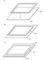
その後、所望の雰囲気下においてガラス基板210を隔壁209に密着させ(図2(C)参照)、加熱処理を行うと、両者が溶着し、ガラス封止体が完成する。当該加熱処理は、ランプやヒーターなどを利用して行う。また、ガラス基板210を隔壁209に密着させた状態で、フラッシュランプを照射し、フリットガラスを瞬時に溶融し固化させてもよい。当該雰囲気は、封止するデバイスの特性にもよるが、例えば、水分や酸素などの少ないものとするとよい。例えば、ドライ窒素やその他の乾燥した気体、代表的には不活性ガスとすればよい。また、これらの混合気体でもよい。フラッシュランプは隔壁209に対し、高いエネルギー密度で照射されるように、隔壁209に沿って配置される。さらにエネルギー密度を高めるために、円筒状のミラーやレンズを用い、光を隔壁209に集めてもよい。これらの構成例については後に記す。フラッシュランプの形状は、隔壁の形状に合わせるとよい。図2に示したように長方形の隔壁を形成する場合は、例えば、細長い円筒状のものを4本用い長方形を形成する。
After that, when the
フラッシュランプには、例えば、発光管の内部に希ガスであるキセノン、クリプトンおよびアルゴンのうちの1種以上が封入されているものを用いる。これにより、例えば、200nm以上1100nm以下の波長領域の光が放射される。これらのランプは、発光時間を10μs以上10ms以下、または100μs以上10ms以下とすることが可能で、局所的に高いエネルギーを与えるのに適している。また、発光管の長さを例えば、1m以上とすることが可能であるため、大型のガラス封止体を作製することができる。この工程の最大の特長は、隔壁209全体を同時に溶融し固化させることができることにある。これにより、隔壁209やそれに接着させるガラス基板208、ガラス基板210の間に応力がほとんど残らないため、衝撃や歪みなどの外力に対して極めて強いガラス封止体を得ることができる。これによる効果は、特に長期間使用したい有機EL照明や有機ELを利用した表示装置を当該ガラス封止体に密封する際、顕著に現れる。なお、局所加熱には、フラッシュランプ以外にレーザや急速加熱ヒーターなどを適用できる。
As the flash lamp, for example, a lamp in which at least one of xenon, krypton, and argon, which are rare gases, is sealed inside the arc tube is used. Thereby, for example, light in a wavelength region of 200 nm to 1100 nm is emitted. These lamps can have a light emission time of 10 μs to 10 ms, or 100 μs to 10 ms, and are suitable for giving high energy locally. Further, since the length of the arc tube can be set to 1 m or more, for example, a large glass sealed body can be manufactured. The greatest feature of this step is that the
次に、図3および図4を用いて複数のガラス封止体を作製する例を示す。まず、装置10より、環状に整形されたペースト452aを吐出させ(図3(A)参照)、ガラス基板450上に隔壁452を複数形成する(図3(B)参照)。隔壁452はいくつあっても構わない。隔壁452は、装置10により形成されるため環状で継ぎ目のないものである。これらを加熱処理しフリットガラスとする。続いて、所望の雰囲気下においてガラス基板451を隔壁452に密着させ(図4(A)参照)、加熱処理を行う。当該加熱処理には、ヒーターやランプ、レーザなどを用いることができる。また、前述したフラッシュランプを用いてもよい。細長い円筒形状のフラッシュランプ453を格子状に配置すると、隔壁452に沿って、光を照射することができる(図4(B)参照)。このとき、隔壁452で形成される各閉空間の間に接着剤を塗布し、ガラス基板450とガラス基板451とを仮止めしてもよい。これにより、隔壁452とガラス基板450とガラス基板451とで形成される閉空間内の雰囲気を、一時的に同閉空間に閉じ込めることができ、フラッシュランプ453を照射する雰囲気を大気中とすることができるため、装置構成が簡易になり好ましい。これは隔壁が1つであっても有効な方法である。また、ガラス基板451を隔壁452に合わせ複数用いても良い。このようにすると、複数のガラス封止体を分離することが容易になる。当該分離には、例えば、レーザスクライバーなどを用いる。
Next, an example in which a plurality of glass sealed bodies is manufactured using FIGS. 3 and 4 will be described. First, an annularly shaped
以上示したように、本発明の一態様であるガラス封止体の隔壁には継ぎ目がないため、本実施の形態によって衝撃や歪みなどの外力に強いガラス封止体を提供することができる。そのため、当該ガラス封止体に保護されたデバイスは長期に渡り、性能を維持できる。 As described above, since the partition wall of the glass sealed body that is one embodiment of the present invention has no seam, this embodiment can provide a glass sealed body that is resistant to external forces such as impact and distortion. Therefore, the device protected by the glass sealing body can maintain performance over a long period of time.
以上、本実施の形態に示す構成、方法などは、他の実施の形態に示す構成、方法などと適宜組み合わせて用いることができる。 The structures, methods, and the like described in this embodiment can be combined as appropriate with any of the structures, methods, and the like described in the other embodiments.
(実施の形態2)
実施の形態1に記載のガラス封止体を用いた本発明の一態様である発光装置の作製方法を、図5および図6を用いて説明する。
(Embodiment 2)
A method for manufacturing a light-emitting device which is one embodiment of the present invention using the glass sealed body described in Embodiment 1 is described with reference to FIGS.
有機EL素子のような発光素子には、電力を供給するための電極が設けられており、これから端子を出し、外部電源に接続できるようになっている。しかしながら、当該端子の設置位置において凸部が形成されるため、封止の密封性が悪くなることがある。当該凸部の弊害を抑える方法の一例は、図6に沿って説明する。 A light emitting element such as an organic EL element is provided with an electrode for supplying electric power, and a terminal can be taken out from the electrode and connected to an external power source. However, since the convex portion is formed at the installation position of the terminal, the sealing performance of the seal may be deteriorated. An example of a method for suppressing the adverse effects of the convex portions will be described with reference to FIG.
まず、図5(A)に示すように、ガラス基板100上に有機EL素子125を設ける。有機EL素子125は、例えば、ガラス基板100に近いほうから陽極、発光層、陰極の順に積まれた積層構造を有する。陽極と陰極を入れ替えてもよい。これらの他に別の層を追加で設けても構わない。陽極からは端子126aが、陰極からは端子126bがそれぞれ出ており、これらを外部電源に接続することで、有機EL素子125に電力を供給できる。
First, as shown in FIG. 5A, an
続いて、図5(B)に示すように、隔壁122を実施の形態1で示した方法により形成する。隔壁122は有機EL素子125を囲むように形成し、端子126a、端子126bの一部を隔壁122の成す閉曲線の外に位置させる。
Subsequently, as illustrated in FIG. 5B, the
通常、端子126a、端子126bには少なからず厚み(代表的には数十nm以上数十μm以下程度)があるため、隔壁122とガラス基板100との密着性が悪くなる部分が生じる可能性がある。加えて、隔壁122最表面の平坦性もそれに沿って損なわれる。これらの不具合を抑制するために、例えば、図6に示すような方法を採用するとよい。
In general, since the terminal 126a and the terminal 126b are not limited in thickness (typically, several tens of nanometers to several tens of micrometers or less), there is a possibility that a portion where the adhesion between the
具体的には、ガラス基板100上に端子301があり、端子301をまたいで隔壁302aを形成すると、図6(A)に示すような隔壁302aと端子301の間の空間や、端子301と重なる隔壁302aの部分に凸部が形成される可能性がある。当該空間はガラス封止体の密封性を著しく損なう可能性があるため、これを出来るだけ小さくする必要がある。また、同様に隔壁302a上の凸部はその上に溶着させる基板との隙間を作る原因となるため、これも出来るだけ小さくしなくてはならない。
Specifically, when the terminal 301 is provided over the
例えば、図6(B)に示すように、隔壁302aを加熱処理する前に、平坦な板303を隔壁302aに押し付けることにより、隔壁302aの形状を変形させ、隔壁302とする。隔壁302aは、加熱処理前なので柔軟性が高く、このような工程が可能である。これにより、隔壁302aと端子301との間の空間や、隔壁302aの最表面に形成される凸部が小さくなるまたは消失する。その後、平坦な板303を隔壁302から離すと、隔壁302の形状が保たれる。平坦な板303を隔壁302の材質と異なるものとすると、接着性が悪いため、平坦な板303を隔壁302に押し付けたまま加熱処理しても構わない。図5で示すように、ガラス基板100上には、熱に弱い有機EL素子125が形成されているため、隔壁122を局所的に加熱し、隔壁122中にあるバインダを揮発させ、さらに粉末ガラス同士を融合させてフリットガラスを得る必要がある。フラッシュランプは局所加熱には有効な手段の1つであるため、ここではフラッシュランプでの加熱処理の例を示す。
For example, as illustrated in FIG. 6B, before the
このとき平坦な板303はフラッシュランプに対し透光性を有している必要があり、例えば、プラスチック基板などが挙げられる。また、ガラス基板100と端子301とに当該透光性があれば、ガラス基板100の下方よりフラッシュランプを照射してもよい。このとき平坦な板303に透光性は問われないため、金属やセラミックスなど、フリットガラスとの接着性の悪い材質のものを採用できる。なお、端子126aおよび端子126bの凸部が無視できるほど小さいものであれば、図6に示したような工程を省くことができる。
At this time, the
また、隔壁122をガラス基板100の表面ではなく、ガラス基板101の表面に設け、端子の凸部と噛み合う凹部を予め隔壁122に設けてもよい。例えば、隔壁122を加熱処理する前に、端子の凸部またはそれと同形状のものを隔壁122に押し付けると、容易に当該凹部を形成できる。勿論、端子126aおよび端子126bの凸部が無視できるほど小さいものであれば、当該凹部の形成工程を省くことができる。隔壁122の加熱処理を行う際は、ガラス基板101の表面に有機EL素子が形成されておらず、局所加熱する必要がないため、ヒーターやランプなどを利用してもよい。また、隔壁122は、ガラス基板100とガラス基板101の双方に設けてもよい。フリットガラス同士を密着させてフラッシュランプを照射することにより、溶着をさらに容易にすることができる。また、ガラス基板100またはガラス基板101に形成された隔壁により、他方の隔壁を囲んでもよい。
Alternatively, the
その後、図5(C)に示すように、ガラス基板101を隔壁122に押し付けた状態で、例えば、フラッシュランプ123により、隔壁122を溶融後固化させ、ガラス基板101と隔壁122を溶着させる。このときの雰囲気は、水分や酸素など有機EL素子に有害なものを極力排除したものとするのが好ましい。具体的には、ドライ窒素や水分の少ないその他の不活性ガスなどを用いるとよい。また、ガラス基板101はガラス基板100と比較して小さなものを用いる。これにより、端子126a、端子126bを露出させることができるため、外部電源への接続を容易にする。なお、局所加熱には、フラッシュランプ以外にレーザや急速加熱ヒーターなどを適用できる。
Thereafter, as shown in FIG. 5C, in a state where the
以上示したように、本発明の一態様であるガラス封止体の隔壁には継ぎ目がないため、本実施の形態によって衝撃や歪みなどの外力に強い発光装置を提供することができる。そのため、当該発光装置は長期に渡り、性能を維持できる。 As described above, since the partition wall of the glass sealed body which is one embodiment of the present invention has no seam, this embodiment can provide a light-emitting device that is resistant to external forces such as impact and distortion. Therefore, the light-emitting device can maintain performance for a long time.
以上、本実施の形態に示す構成、方法などは、他の実施の形態に示す構成、方法などと適宜組み合わせて用いることができる。 The structures, methods, and the like described in this embodiment can be combined as appropriate with any of the structures, methods, and the like described in the other embodiments.
(実施の形態3)
先の実施の形態に記載のフラッシュランプに適用する光学系の例を、図7を用いて説明する。図7には、ガラス基板100上に本発明の一態様に係る継ぎ目の無い隔壁122が形成されており、ガラス基板101が隔壁122に密着された状態を示している。
(Embodiment 3)
An example of an optical system applied to the flash lamp described in the above embodiment will be described with reference to FIG. In FIG. 7, a
図7(A)に示すように、円筒状のミラー127をフラッシュランプ123に被せることで、四方に広がる光を一方向に集めることが可能となる。例えば、図7の紙面に平行な方向における円筒状のミラー127の断面形状を楕円とし、当該楕円の焦点にフラッシュランプ123を配置し、他の焦点に隔壁122を配置することにより、光を効率よく隔壁122に集めることができる。
As shown in FIG. 7A, by covering a
その他の例として、図7(B)に示すように、フラッシュランプ123と隔壁122の間に、凸レンズ128を設け、広がる光を収束させてもよい。また、ミラー127と凸レンズ128とを組み合わせて用いてもよい。これらの光学系を用いてフラッシュランプ123を発光させると少ないエネルギーで隔壁122とガラス基板101とを溶着できる。
As another example, a
隔壁122には継ぎ目がなく、また、本実施の形態に示すフラッシュランプと組み合わせて用いると、隔壁122全体を同時に加熱処理できるため溶着時の歪みの発生がほとんどなく、本実施の形態によって衝撃や歪みなどの外力に強いガラス封止体を提供することができる。そのため、当該ガラス封止体に保護されたデバイスは長期に渡り、性能を維持できる。
The
以上、本実施の形態に示す構成、方法などは、他の実施の形態に示す構成、方法などと適宜組み合わせて用いることができる。 The structures, methods, and the like described in this embodiment can be combined as appropriate with any of the structures, methods, and the like described in the other embodiments.
(実施の形態4)
本実施の形態では、先の実施の形態に示した環状に整形されたペーストを吐出する装置の他の一例を図8に示す。
(Embodiment 4)
In this embodiment, FIG. 8 illustrates another example of a device that discharges an annularly shaped paste described in the above embodiment.
図8(A)は平面図、図8(B)は、図8(A)中の鎖線M−Nで切断した断面図である。配管251は、ペースト252を環状のノズル253に供給するディスペンス装置(図示しない)に接続されている。当該ディスペンス装置により、ペースト252がノズル253内部に満たされる。その後、環状に配置された圧電素子254に電圧を加えて変形させ、圧電素子254aとすることで、環状に整形されたペースト252aを吐出させる(図8(C)参照)。圧電素子254に加える電圧によりペーストの吐出量を制御することができるため、最適な吐出量を選択できる。これにより、ガラス基板255上に閉曲線でできた隔壁が形成される。図8では、圧電素子254を一体物として図示したが、細かく分けて環状に配置してもよい。このようにすることで、圧電素子254の変形の程度を局所的に変えることができるため、局所的にペーストの吐出量を変えることができる。このため、例えば、実施の形態2に示した電極の端子126aおよび端子126b上でペーストの吐出量を減らすことで隔壁122表面の平坦性などを改善することができる。本実施の形態では、ペースト252aの形状を長方形としたが、その他の閉曲線としても構わない。その後、先の実施の形態に示した要領でガラス封止体を形成する。
8A is a plan view, and FIG. 8B is a cross-sectional view taken along a chain line MN in FIG. 8A. The
以上示したように、本発明の一態様であるガラス封止体の隔壁には継ぎ目がないため、本実施の形態によって衝撃や歪みなどの外力に強いガラス封止体を提供することができる。そのため、当該ガラス封止体に保護されたデバイスは長期に渡り、性能を維持できる。 As described above, since the partition wall of the glass sealed body that is one embodiment of the present invention has no seam, this embodiment can provide a glass sealed body that is resistant to external forces such as impact and distortion. Therefore, the device protected by the glass sealing body can maintain performance over a long period of time.
以上、本実施の形態に示す構成、方法などは、他の実施の形態に示す構成、方法などと適宜組み合わせて用いることができる。 The structures, methods, and the like described in this embodiment can be combined as appropriate with any of the structures, methods, and the like described in the other embodiments.
(実施の形態5)
本実施の形態では、先の実施の形態に示した環状に整形されたペーストを吐出する装置の他の一例を図9に示す。
(Embodiment 5)
In this embodiment, FIG. 9 illustrates another example of a device that discharges an annularly shaped paste described in the above embodiment.
図9(A)は平面図、図9(B)は、図9(A)中の鎖線O−Pで切断した断面図である。配管261は、ペースト262を環状のノズル263に供給するディスペンス装置(図示しない)に接続されている。当該ディスペンス装置により、ペースト262がノズル263内部に満たされる。その後、環状に配置された急速加熱ヒーター264を加熱させ、その周辺のペースト262に泡266を発生させることにより、環状に整形されたペースト262aを吐出させる(図9(C)参照)。これにより、ガラス基板265上に閉曲線でできた隔壁が形成される。図9では、急速加熱ヒーター264を一体物として図示したが、細かく分けて環状に配置してもよい。このようにすることで、急速加熱ヒーター264の加熱温度を局所的に変えることができるため、局所的にペーストの吐出量を変えることができる。このため、例えば、実施の形態2に示した電極の端子126aおよび端子126b上でペーストの吐出量を減らすことで隔壁122表面の平坦性などを改善することができる。本実施の形態では、ペースト262aの形状を長方形としたが、その他の閉曲線としても構わない。その後、先の実施の形態に示した要領でガラス封止体を形成する。
9A is a plan view, and FIG. 9B is a cross-sectional view taken along a chain line OP in FIG. 9A. The
以上示したように、本発明の一態様であるガラス封止体の隔壁には継ぎ目がないため、本実施の形態によって衝撃や歪みなどの外力に強いガラス封止体を提供することができる。そのため、当該ガラス封止体に保護されたデバイスは長期に渡り、性能を維持できる。 As described above, since the partition wall of the glass sealed body that is one embodiment of the present invention has no seam, this embodiment can provide a glass sealed body that is resistant to external forces such as impact and distortion. Therefore, the device protected by the glass sealing body can maintain performance over a long period of time.
以上、本実施の形態に示す構成、方法などは、他の実施の形態に示す構成、方法などと適宜組み合わせて用いることができる。 The structures, methods, and the like described in this embodiment can be combined as appropriate with any of the structures, methods, and the like described in the other embodiments.
(実施の形態6)
実施の形態2に記載の有機EL素子125の一態様について、図10(A)を用いて説明する。理解を容易にするため、端子126a、端子126bについては言及しない。
(Embodiment 6)
One mode of the
発光素子は、一対の電極(第1の電極102および第2の電極104)と、当該一対の電極間に挟まれた有機EL層103を有する。また、本実施の形態で説明する発光素子は、ガラス基板100上に設けられている。
The light-emitting element includes a pair of electrodes (a
ガラス基板100は、発光素子の支持体として用いられる。ガラス基板100としては、長方形の板状のものは勿論、曲面を有するものなど様々な形状のものを用いることができる。
The
第1の電極102および第2の電極104は、一方が陽極として機能し、他方が陰極として機能する。本実施の形態においては、第1の電極102を陽極として用い、第2の電極104を陰極として用いるものとして説明するが、本発明はこの構成に限定されるものではない。
One of the
陽極として用いる材料は、仕事関数の大きい(具体的には4.0eV以上)金属、合金、導電性化合物、またはこれらの混合物などが好ましい。具体的には、酸化インジウム−酸化スズ(ITO:Indium Tin Oxide)、シリコン若しくは酸化シリコンを含有した酸化インジウム−酸化スズ、酸化インジウム−酸化亜鉛、酸化亜鉛を含む酸化タングステン−酸化インジウム等が挙げられる。この他、金(Au)、白金(Pt)、ニッケル(Ni)、タングステン(W)、クロム(Cr)、モリブデン(Mo)、鉄(Fe)、コバルト(Co)、銅(Cu)、パラジウム(Pd)、または金属材料の窒化物(例えば、窒化チタン)等が挙げられる。 The material used as the anode is preferably a metal, an alloy, a conductive compound, or a mixture thereof having a high work function (specifically, 4.0 eV or more). Specific examples include indium tin oxide (ITO), indium oxide-tin oxide containing silicon or silicon oxide, indium oxide-zinc oxide, tungsten oxide-indium oxide containing zinc oxide, and the like. . In addition, gold (Au), platinum (Pt), nickel (Ni), tungsten (W), chromium (Cr), molybdenum (Mo), iron (Fe), cobalt (Co), copper (Cu), palladium ( Pd), or a nitride of a metal material (for example, titanium nitride).
陰極として用いる材料は、仕事関数の小さい(具体的には3.8eV以下)金属、合金、電気伝導性化合物、またはこれらの混合物などが好ましい。具体的には、元素周期表の第1族または第2族に属する元素、すなわち、リチウム(Li)やセシウム(Cs)等のアルカリ金属、カルシウム(Ca)、ストロンチウム(Sr)等のアルカリ土類金属、マグネシウム(Mg)が挙げられる。また、アルカリ金属またはアルカリ土類金属を含む合金(例えば、MgAg、AlLi)を用いることもできる。また、ユウロピウム(Eu)、イッテルビウム(Yb)などの希土類金属、または希土類金属を含む合金を用いることもできる。また、有機EL層103の一部として、第2の電極104に接する電子注入層を設ける場合、仕事関数の大小に関わらず、Al、Ag、ITOなどの様々な導電性材料を第2の電極104として用いることができる。これら導電性材料は、スパッタリング法やインクジェット法、スピンコート法等を用いて薄膜とすることが可能である。
The material used as the cathode is preferably a metal, an alloy, an electrically conductive compound, or a mixture thereof having a low work function (specifically, 3.8 eV or less). Specifically, elements belonging to Group 1 or Group 2 of the periodic table of elements, that is, alkali metals such as lithium (Li) and cesium (Cs), alkaline earths such as calcium (Ca) and strontium (Sr) A metal, magnesium (Mg) is mentioned. Alternatively, an alloy containing an alkali metal or an alkaline earth metal (eg, MgAg, AlLi) can be used. Alternatively, a rare earth metal such as europium (Eu) or ytterbium (Yb), or an alloy containing a rare earth metal can be used. Further, when an electron injection layer in contact with the
有機EL層103は、単層構造で構成されることも可能であるが、通常、積層構造から構成される。有機EL層103の積層構造については特に限定されず、電子輸送性の高い物質を含む層(電子輸送層)または正孔輸送性の高い物質を含む層(正孔輸送層)、電子注入性の高い物質を含む層(電子注入層)、正孔注入性の高い物質を含む層(正孔注入層)、バイポーラ性(電子および正孔の輸送性の高い物質)の物質を含む層、発光材料を含む層(発光層)などを適宜組み合わせて構成すればよい。例えば、正孔注入層、正孔輸送層、発光層、電子輸送層、電子注入層等を適宜組み合わせて構成することができる。図10(A)においては、第1の電極102の上に形成された有機EL層103として、正孔注入層111、正孔輸送層112、発光層113、電子輸送層114が順に積層された構造を示している。
The
発光素子は、第1の電極102と第2の電極104との間に生じた電位差により電流が流れ、発光性の高い物質を含む層である発光層113において正孔と電子とが再結合し、発光するものである。つまり、発光層113に発光領域が形成されるような構成となっている。
In the light-emitting element, current flows due to a potential difference generated between the
発光は、第1の電極102または第2の電極104のいずれか一方または両方を通って外部に取り出される。従って、第1の電極102または第2の電極104のいずれか一方または両方は、透光性を有する電極でなる。第1の電極102のみが透光性を有する電極である場合、発光は第1の電極102を通って基板側から取り出される。また、第2の電極104のみが透光性を有する電極である場合、発光は第2の電極104を通って基板と逆側から取り出される。第1の電極102および第2の電極104がいずれも透光性を有する電極である場合、発光は第1の電極102および第2の電極104を通って、基板側および基板と逆側の両方から取り出される。
Light emission is extracted outside through one or both of the
発光層113に接する正孔輸送層112や電子輸送層114、特に発光層113における発光領域に近い方に接するキャリア(電子または正孔)輸送層は、発光層113で生成した励起子からのエネルギー移動を抑制するため、発光層を構成する発光材料、または発光層に含まれる発光中心物質よりも大きなエネルギーギャップを有する物質で構成することが好ましい。
The
正孔注入層111は、正孔注入性の高い物質を含み、第1の電極102から正孔輸送層112へ正孔の注入を補助する機能を有する。正孔注入層111には、第1の電極102と正孔輸送層112との間のイオン化ポテンシャルの差を緩和し、正孔が注入され易くなるものを選ぶ。具体的には、正孔注入層111は、イオン化ポテンシャルを正孔輸送層112よりも小さく、第1の電極102よりも大きいものとするか、正孔輸送層112と第1の電極102との間に1〜2nmの薄膜として設けたときにエネルギーバンドを曲げるものを用いて形成することが好ましい。正孔注入性の高い物質には、フタロシアニン(略称:H2Pc)や銅フタロシアニン(CuPc)等のフタロシアニン系の化合物、またはポリ(エチレンジオキシチオフェン)/ポリ(スチレンスルホン酸)水溶液(PEDOT/PSS)等の高分子がある。
The
正孔輸送層112は、正孔輸送性の高い物質を含む。正孔輸送性の高い物質とは、正孔の移動度が電子のそれよりも高いものを指し、電子の移動度に対する正孔の移動度の比(=正孔移動度/電子移動度)が100よりも大きいものを利用するのが好ましい。また、正孔輸送層112の正孔移動度は、1×10−6cm2/Vs以上とするのが好ましい。具体的には、4,4’−ビス[N−(1−ナフチル)−N−フェニルアミノ]ビフェニル(略称:NPB)、4,4’−ビス[N−(3−メチルフェニル)−N−フェニルアミノ]ビフェニル(略称:TPD)、4,4’,4’’−トリス(N,N−ジフェニルアミノ)トリフェニルアミン(略称:TDATA)、4,4’,4’’−トリス[N−(3−メチルフェニル)−N−フェニルアミノ]トリフェニルアミン(略称:MTDATA)、4,4’−ビス{N−[4−(N,N−ジ−m−トリルアミノ)フェニル]−N−フェニルアミノ}ビフェニル(略称:DNTPD)、1,3,5−トリス[N,N−ジ(m−トリル)アミノ]ベンゼン(略称:m−MTDAB)、4,4’,4’’−トリス(N−カルバゾリル)トリフェニルアミン(略称:TCTA)、フタロシアニン(略称:H2Pc)、銅フタロシアニン(略称:CuPc)、バナジルフタロシアニン(略称:VOPc)などを利用できる。また、正孔輸送層112は、単層構造としてもよいし、積層構造としてもよい。
The
電子輸送層114は、電子輸送性の高い物質を含む。電子輸送性の高い物質とは、電子の移動度が正孔のそれよりも高いものを指し、正孔の移動度に対する電子の移動度の比(=電子移動度/正孔移動度)が100よりも大きいものを利用するのが好ましい。また、電子輸送層114の電子移動度は、1×10−6cm2/Vs以上とするのが好ましい。具体的には、キノリン骨格を有する金属錯体、ベンゾキノリン骨格を有する金属錯体、オキサゾール系配位子を有する金属錯体、チアゾール系配位子を有する金属錯体を利用できる。キノリン骨格を有する金属錯体の具体例としては、トリス(8−キノリノラト)アルミニウム(略称:Alq3)、トリス(4−メチル−8−キノリノラト)アルミニウム(略称:Almq3)、ビス(2−メチル−8−キノリノラト)(4−フェニルフェノラト)アルミニウム(略称:BAlq)が挙げられる。また、ベンゾキノリン骨格を有する金属錯体の具体例としては、ビス(10−ヒドロキシベンゾ[h]キノリナト)ベリリウム(略称:BeBq2)が挙げられる。また、オキサゾール系配位子を有する金属錯体の具体例としては、ビス[2−(2−ヒドロキシフェニル)ベンズオキサゾラト]亜鉛(略称:Zn(BOX)2)が挙げられる。また、チアゾール系配位子を有する金属錯体の具体例としては、ビス[2−(2−ヒドロキシフェニル)ベンゾチアゾラト]亜鉛(略称:Zn(BTZ)2)が挙げられる。また、金属錯体以外にも、2−(4−ビフェニリル)−5−(4−tert−ブチルフェニル)−1,3,4−オキサジアゾール(略称:PBD)や、1,3−ビス[5−(p−tert−ブチルフェニル)−1,3,4−オキサジアゾール−2−イル]ベンゼン(略称:OXD−7)、3−(4−ビフェニリル)−4−フェニル−5−(4−tert−ブチルフェニル)−1,2,4−トリアゾール(略称:TAZ 01)、バソフェナントロリン(略称:BPhen)、バソキュプロイン(略称:BCP)なども用いることができる。具体例を挙げた上述の物質は、主に10−6cm2/Vs以上の電子移動度を有する物質である。なお、正孔よりも電子の輸送性の高い物質であれば、これら以外の物質を電子輸送層114として用いてもよい。また、電子輸送層114は、単層構造としてもよいし、積層構造としてもよい。 The electron transport layer 114 includes a substance having a high electron transport property. A substance having a high electron transporting property refers to a substance having electron mobility higher than that of holes, and the ratio of electron mobility to hole mobility (= electron mobility / hole mobility) is 100. It is preferable to use a larger one. The electron mobility of the electron transport layer 114 is preferably 1 × 10 −6 cm 2 / Vs or higher. Specifically, a metal complex having a quinoline skeleton, a metal complex having a benzoquinoline skeleton, a metal complex having an oxazole ligand, and a metal complex having a thiazole ligand can be used. Specific examples of the metal complex having a quinoline skeleton include tris (8-quinolinolato) aluminum (abbreviation: Alq 3 ), tris (4-methyl-8-quinolinolato) aluminum (abbreviation: Almq 3 ), bis (2-methyl- 8-quinolinolato) (4-phenylphenolato) aluminum (abbreviation: BAlq). As a specific example of the metal complex having a benzoquinoline skeleton, bis (10-hydroxybenzo [h] quinolinato) beryllium (abbreviation: BeBq 2 ) can be given. As a specific example of a metal complex having an oxazole-based ligand, bis [2- (2-hydroxyphenyl) benzoxazolate] zinc (abbreviation: Zn (BOX) 2 ) can be given. As a specific example of a metal complex having a thiazole-based ligand, bis [2- (2-hydroxyphenyl) benzothiazolate] zinc (abbreviation: Zn (BTZ) 2 ) can be given. In addition to metal complexes, 2- (4-biphenylyl) -5- (4-tert-butylphenyl) -1,3,4-oxadiazole (abbreviation: PBD), 1,3-bis [5 -(P-tert-butylphenyl) -1,3,4-oxadiazol-2-yl] benzene (abbreviation: OXD-7), 3- (4-biphenylyl) -4-phenyl-5- (4- tert-Butylphenyl) -1,2,4-triazole (abbreviation: TAZ 01), bathophenanthroline (abbreviation: BPhen), bathocuproin (abbreviation: BCP), and the like can also be used. The above-described substances with specific examples are mainly substances having an electron mobility of 10 −6 cm 2 / Vs or more. Note that a substance other than these substances may be used for the electron-transport layer 114 as long as it has a property of transporting more electrons than holes. Further, the electron transport layer 114 may have a single-layer structure or a stacked structure.
また、発光層113と電子輸送層114との間に電子キャリアの移動を制御する層を設けてもよい。電子キャリアの移動を制御する層は、上述したような電子輸送性の高い材料に対して、電子トラップ性の高い物質を少量添加した層である。電子キャリアの移動を制御する層を設けることにより、電子キャリアの移動を抑制し、キャリアバランスを調節することが可能となる。このような構成は、発光層を電子が突き抜けてしまうことにより発生する問題(例えば、素子寿命の低下)の抑制に大きな効果を発揮する。
Further, a layer for controlling the movement of electron carriers may be provided between the light-emitting
また、電子輸送層114と第2の電極104との間に、第2の電極104に接して電子注入層を設けてもよい。電子注入層としては、電子輸送性を有する物質からなる層中に、フッ化リチウム(LiF)、フッ化セシウム(CsF)、フッ化カルシウム(CaF2)などのようなアルカリ金属、アルカリ土類金属、またはそれらの化合物を含有させたものを用いればよい。具体例としては、Alq3中にマグネシウム(Mg)を含有させたものを用いることができる。電子注入層を設けることにより、第2の電極104からの電子注入を効率良く行うことができる。
Further, an electron injection layer may be provided in contact with the
また、有機EL層103は、乾式法、湿式法を問わず、種々の方法を用いて形成できる。例えば、真空蒸着法、インクジェット法、またはスピンコート法を用いることができる。また、有機EL層103を積層構造とする場合、各層毎に異なる方法を用いて形成してもよいし、各層全てを同一の方法で形成してもよい。
The
また、第1の電極102、第2の電極104は、ゾル−ゲル法や液状の金属材料を用いた湿式法で形成してもよいし、スパッタリング法や真空蒸着法などの乾式法で形成してもよい。このような発光素子と本発明の一態様であるガラス封止体を組み合わせることにより、より長寿命で衝撃や歪みなどの外力に強い発光装置を得ることができる。
The
以上、本実施の形態に示す構成、方法などは、他の実施の形態に示す構成、方法などと適宜組み合わせて用いることができる。 The structures, methods, and the like described in this embodiment can be combined as appropriate with any of the structures, methods, and the like described in the other embodiments.
(実施の形態7)
本実施の形態では、本発明の一態様として、複数の発光ユニットを積層した構成を有する発光素子(以下、「タンデム型の発光素子」という)について、図10(B)を参照しながら説明する。タンデム型の発光素子は、第1の電極と第2の電極との間に、複数の発光ユニットを有する。発光ユニットとしては、先に示した有機EL層103と同様な構成を用いることができる。
(Embodiment 7)
In this embodiment, as one embodiment of the present invention, a light-emitting element having a structure in which a plurality of light-emitting units is stacked (hereinafter referred to as a “tandem light-emitting element”) is described with reference to FIG. . A tandem light-emitting element includes a plurality of light-emitting units between a first electrode and a second electrode. As the light emitting unit, a structure similar to that of the
図10(B)において、第1の電極501と第2の電極502との間には、第1の発光ユニット511と第2の発光ユニット512が積層されている。第1の電極501と第2の電極502は、実施の形態6と同様なものを適用することができる。また、第1の発光ユニット511と第2の発光ユニット512は同じ構成であっても異なる構成であってもよく、各ユニットの構成は、それぞれ実施の形態6に示したものと同様なものを適用することができる。
In FIG. 10B, a first light-emitting
第1の発光ユニット511と第2の発光ユニット512との間には、電荷発生層513が設けられている。電荷発生層513は、有機化合物と金属酸化物の複合材料を含み、第1の電極501と第2の電極502に電圧を印加したときに、一方の側の発光ユニットに電子を注入し、他方の側の発光ユニットに正孔を注入する機能を有する。有機化合物と金属酸化物の複合材料は、キャリア注入性、キャリア輸送性に優れているため、低電圧駆動、低電流駆動を可能にする。
A
正孔輸送性の有機化合物には、正孔移動度が10−6cm2/Vs以上であるものを用いることが好ましい。具体的には、芳香族アミン化合物、カルバゾール化合物、芳香族炭化水素、高分子化合物(オリゴマー、デンドリマー、ポリマー等)などが利用できる。また、それらと混ぜる金属酸化物には、元素周期表における第4族乃至第8族に属する金属の酸化物を用いればよく、具体的には、酸化バナジウム、酸化ニオブ、酸化タンタル、酸化クロム、酸化モリブデン、酸化タングステン、酸化マンガン、酸化レニウムが挙げられ、これらの金属酸化物は電子受容性が高いため、好ましい。特に、酸化モリブデンは大気中でも安定であり、吸湿性が低く、かつ扱いやすいため、特に好ましい。 As the hole-transporting organic compound, an organic compound having a hole mobility of 10 −6 cm 2 / Vs or higher is preferably used. Specifically, aromatic amine compounds, carbazole compounds, aromatic hydrocarbons, polymer compounds (oligomers, dendrimers, polymers, etc.) can be used. Further, as the metal oxide mixed with them, an oxide of a metal belonging to Group 4 to Group 8 in the periodic table of elements may be used. Specifically, vanadium oxide, niobium oxide, tantalum oxide, chromium oxide, Examples thereof include molybdenum oxide, tungsten oxide, manganese oxide, and rhenium oxide, and these metal oxides are preferable because of their high electron accepting properties. Molybdenum oxide is particularly preferable because it is stable in the air, has a low hygroscopic property, and is easy to handle.
また、電荷発生層513は、単層構造でもよいし、積層構造でもよい。例えば、有機化合物と金属酸化物の複合材料を含む層と、電子供与性物質の中から選ばれた一の化合物、および電子輸送性の高い化合物を含む層とを積層した構造としてもよいし、有機化合物と金属酸化物の複合材料を含む層と、透明導電膜とを積層した構造としてもよい。
The
本実施の形態では、2つの発光ユニットを有する発光素子について説明したが、本発明はこの構成に限定されるものではない。すなわち、タンデム型の発光素子は、3つ以上の発光ユニットを有していてもよい。この場合も、各発光ユニットの間には電荷発生層を設ける。例えば、第1のユニットと、それよりも長波長の発光(例えば、赤色の発光)を呈する第1の発光材料を用いて作製される第2のユニットと、第1のユニットよりも長波長、かつ第1の発光材料よりも短波長の発光(例えば、緑色の発光)を呈する第2の発光材料を用いて作製される第3のユニットとを有する発光素子を構成してもよい。これらの発光ユニットを用いることにより、白色の発光装置を得ることができる。 Although the light-emitting element having two light-emitting units has been described in this embodiment mode, the present invention is not limited to this structure. That is, the tandem light-emitting element may include three or more light-emitting units. Also in this case, a charge generation layer is provided between the light emitting units. For example, a first unit, a second unit manufactured using a first light-emitting material that emits light having a longer wavelength (for example, red light), and a longer wavelength than the first unit, In addition, a light-emitting element including a third unit manufactured using a second light-emitting material that emits light having a shorter wavelength than the first light-emitting material (for example, green light emission) may be configured. By using these light emitting units, a white light emitting device can be obtained.
本実施の形態に係るタンデム型の発光素子は、一対の電極間に複数の発光ユニットを電荷発生層で仕切って配置するため、電流密度を低く保ったまま高輝度の発光を可能にする。電流密度を低くできるため、高輝度でも長寿命な発光素子とすることができる。このような発光素子と本発明の一態様であるガラス封止体を組み合わせることにより、より長寿命で衝撃や歪みなどの外力に強い発光装置を得ることができる。 In the tandem light-emitting element according to this embodiment, a plurality of light-emitting units are partitioned by a charge generation layer between a pair of electrodes, and thus high-luminance light emission is possible while keeping a current density low. Since the current density can be reduced, a light-emitting element with high luminance and a long lifetime can be obtained. By combining such a light-emitting element and the glass sealed body that is one embodiment of the present invention, a light-emitting device that has a longer life and is resistant to external forces such as impact and distortion can be obtained.
以上、本実施の形態に示す構成、方法などは、他の実施の形態に示す構成、方法などと適宜組み合わせて用いることができる。 The structures, methods, and the like described in this embodiment can be combined as appropriate with any of the structures, methods, and the like described in the other embodiments.
(実施の形態8)
本実施の形態では、本発明の一態様であるガラス封止体により封止された、パッシブマトリクス型の発光装置、およびアクティブマトリクス型の発光装置について説明する。
(Embodiment 8)
In this embodiment, a passive matrix light-emitting device and an active matrix light-emitting device which are sealed with a glass sealing body that is one embodiment of the present invention will be described.
図11および図12にパッシブマトリクス型の発光装置の例を示す。 11 and 12 show examples of passive matrix light-emitting devices.
パッシブマトリクス型(単純マトリクス型ともいう)の発光装置は、ストライプ状(帯状)に並列された複数の陽極と、ストライプ状に並列された複数の陰極とが互いに直交するように設けられており、その交差部に発光層が挟まれた構造となっている。従って、選択された(電圧が印加された)陽極と選択された陰極との交点にあたる画素が点灯することになる。 A light emitting device of a passive matrix type (also referred to as a simple matrix type) is provided so that a plurality of anodes arranged in stripes (bands) and a plurality of cathodes arranged in stripes are orthogonal to each other. The light emitting layer is sandwiched between the intersections. Therefore, the pixel corresponding to the intersection between the selected anode (to which voltage is applied) and the selected cathode is turned on.
図11(A)乃至図11(C)は、封止前における画素部の平面図であり、図11(A)乃至図11(C)中の鎖線A−A’で切断した断面を図11(D)に示す。 11A to 11C are plan views of the pixel portion before sealing, and a cross section taken along a chain line AA ′ in FIGS. 11A to 11C is shown in FIG. Shown in (D).
ガラス基板601上には、下地絶縁層として絶縁層602が形成されている。なお、絶縁層602が必要でなければ特に形成しなくともよい。絶縁層602上には、ストライプ状の複数の第1の電極603が等間隔で配置されている(図11(A)参照)。なお、本実施の形態で示す第1の電極603は、実施の形態6における第1の電極102に相当する。
An insulating
また、第1の電極603上には、各画素に対応する開口部605を有する隔壁604が設けられている。隔壁604は、絶縁材料で形成されている。例えば、ポリイミド、アクリル、ポリアミド、ポリイミドアミド、レジスト、もしくはベンゾシクロブテン等の感光性または非感光性の有機材料や、アルキル基を含むSiOx膜等のSOG膜を絶縁材料として用いることができる。また、各画素に対応する開口部605は、発光領域となる(図11(B)参照)。
A
開口部605を有する隔壁604上には、第1の電極603と交差する複数の隔壁606が設けられている(図11(C)参照)。複数の隔壁606は、それぞれ互いに平行に設けられており、逆テーパ状をなしている。
A plurality of
第1の電極603および隔壁604上には、有機EL層607および第2の電極608が順次積層されている(図11(D)参照)。なお、本実施の形態で示す有機EL層607は、実施の形態6における有機EL層103に相当し、第2の電極608は、第2の電極104に相当する。隔壁604および隔壁606を合わせた高さは、有機EL層607および第2の電極608を合わせた厚さより大きくなるように設定されているため、図11(D)に示すように複数の領域に分離された有機EL層607、および第2の電極608が形成される。なお、複数に分離された領域は、それぞれ電気的に独立している。
An
第2の電極608は、第1の電極603と交差するストライプをなす。なお、有機EL層607および第2の電極608を形成すると、逆テーパ状の隔壁606上にも同様の層が形成されるが、有機EL層607、および第2の電極608とは分断されている。
The
続いて、ガラス基板601を基に実施の形態2で示したようにガラス封止体を形成する。これにより、発光素子の劣化を著しく抑制できる。なお、密閉された空間には、乾燥した充填材や不活性ガスを充填しても良い。さらに、水分などによる発光素子の劣化を防ぐために当該ガラス封止体に乾燥材などを封入してもよい。乾燥剤によって微量な水分が除去され、十分乾燥される。乾燥剤としては、酸化カルシウムや酸化バリウムなどのアルカリ土類金属の酸化物、ゼオライト、またはシリカゲル等を用いることができる。アルカリ土類金属の酸化物は、化学吸着によって水分を吸収する性質を有する。また、ゼオライトやシリカゲルは、物理吸着によって水分を吸着する性質を有する。
Subsequently, a glass sealing body is formed based on the
次に、図11(A)乃至図11(D)に示したパッシブマトリクス型の発光装置にFPC(フレキシブルプリントサーキット)などを実装したものの平面図を図12に示す。 Next, FIG. 12 shows a plan view of the passive matrix light emitting device shown in FIGS. 11A to 11D in which an FPC (flexible printed circuit) or the like is mounted.
図12において、画像表示を構成する画素部では、走査線群とデータ線群が互いに直交している。 In FIG. 12, in the pixel portion constituting the image display, the scanning line group and the data line group are orthogonal to each other.
ここで図12の図11との関係を示すと、第1の電極603が走査線703に相当し、第2の電極608がデータ線708に相当し、逆テーパ状の隔壁606が隔壁706に相当する。データ線708と走査線703の間には、図11に示した有機EL層607が挟まれており、領域705で示される交差部が画素1つ分となる。
Here, the relationship between FIG. 11 and FIG. 11 shows that the
走査線703は配線端で接続配線709と電気的に接続され、接続配線709が入力端子710を介してFPC711bに接続される。また、データ線708は入力端子712を介してFPC711aに接続される。データ線708と接続配線709は、図5に示した端子126a、端子126bに相当する。これらをまたいでフリットガラスの隔壁を形成し、例えば、先の実施の形態に示した方法により、ガラス封止体を形成する。
The
また、必要に応じて、光の射出面に偏光板、円偏光板(楕円偏光板を含む)、位相差板(λ/4板、λ/2板)、カラーフィルタなどの光学フィルムを適宜設けてもよい。また、偏光板または円偏光板に加えて反射防止膜を設け、外光の反射を抑えてもよい。あるいは、光の射出面に凹凸を設け、反射光を拡散させることにより、外光が光の射出面に映り込むのを抑えることができる。 If necessary, optical films such as a polarizing plate, a circular polarizing plate (including an elliptical polarizing plate), a retardation plate (λ / 4 plate, λ / 2 plate), and a color filter are appropriately provided on the light exit surface. May be. In addition to a polarizing plate or a circularly polarizing plate, an antireflection film may be provided to suppress reflection of external light. Alternatively, it is possible to prevent external light from being reflected on the light exit surface by providing irregularities on the light exit surface and diffusing the reflected light.
なお、図12では、駆動回路を基板上に設けない例を示したが、基板上に駆動回路を有するICチップを設けてもよい。 Note that although FIG. 12 illustrates an example in which the driver circuit is not provided over the substrate, an IC chip having the driver circuit may be provided over the substrate.
ICチップを用いる場合には、画素部の周辺(外側)の領域に、画素部へ各信号を伝送する駆動回路が形成されたデータ線側IC、走査線側ICをそれぞれ取り付ける。取り付け方式には、COG方式、TCP、ワイヤボンディング方式等を用いることができる。TCPはTABテープにICを設けたものであり、TABテープを素子形成基板上の配線に接続してICを取り付ける。データ線側ICおよび走査線側ICは、シリコン基板やSOI(Silicon On Insulator)基板に形成されたものであってもよいし、ガラス基板、石英基板、またはプラスチック基板上に形成されたものであってもよい。 In the case of using an IC chip, a data line side IC and a scanning line side IC in which a driving circuit for transmitting each signal to the pixel portion is formed are attached to the periphery (outside) of the pixel portion. For the attachment method, a COG method, TCP, a wire bonding method, or the like can be used. TCP is a TAB tape provided with an IC, and the TAB tape is connected to a wiring on an element formation substrate to attach the IC. The data line side IC and the scanning line side IC may be formed on a silicon substrate or an SOI (Silicon On Insulator) substrate, or may be formed on a glass substrate, a quartz substrate, or a plastic substrate. May be.
次に、アクティブマトリクス型の発光装置の例について、図13を用いて説明する。なお、図13(A)は発光装置を示す平面図であり、図13(B)は図13(A)を鎖線B−B’で切断した断面図である。本実施の形態に係るアクティブマトリクス型の発光装置は、ガラス基板801上に設けられた画素部802と、駆動回路部(ソース側駆動回路)803と、駆動回路部(ゲート側駆動回路)804とを有する。画素部802、駆動回路部803、および駆動回路部804は、隔壁805とガラス基板801とガラス基板806とで形成されたガラス封止体の中に封止されている。
Next, an example of an active matrix light-emitting device is described with reference to FIGS. 13A is a plan view showing the light-emitting device, and FIG. 13B is a cross-sectional view taken along the chain line B-B ′ of FIG. 13A. An active matrix light-emitting device according to this embodiment includes a
ガラス基板801上には、駆動回路部803および駆動回路部804に外部からの信号(ビデオ信号、クロック信号、スタート信号、またはリセット信号等)や電位を伝達する外部入力端子を接続するための引き回し配線807が設けられる。ここでは、外部入力端子としてFPC808を設ける例を示している。なお、ここではFPCしか図示されていないが、このFPCにはプリント配線基板(PWB)が取り付けられていてもよい。本明細書における発光装置は、発光装置本体だけでなく、発光装置本体にFPCまたはPWBが取り付けられた状態のものも範疇に含むものとする。
On the
次に、アクティブマトリクス型の発光装置の断面構造について図13(B)を用いて説明する。なお、ガラス基板801上には駆動回路部803および駆動回路部804および画素部802が形成されているが、図13(B)においては、ソース側駆動回路である駆動回路部803と、画素部802を示している。
Next, a cross-sectional structure of the active matrix light-emitting device is described with reference to FIG. Note that a
駆動回路部803は、nチャネル型TFT809とpチャネル型TFT810とを組み合わせたCMOS回路を有する例を示している。なお、駆動回路部は、種々のCMOS回路、PMOS回路、またはNMOS回路で形成することができる。また、本実施の形態では、同一基板上に画素部と駆動回路が形成されたドライバー一体型を示すが、本発明はこの構成に限定されるものではなく、画素部が形成された基板とは別の基板に駆動回路を形成することもできる。
In the example, the
画素部802は、スイッチング用のTFT811と、電流制御用のTFT812と、電流制御用のTFT812の配線(ソース電極またはドレイン電極)に電気的に接続された陽極813とを含む複数の画素により形成されている。また、陽極813の端部を覆って絶縁物814が形成されている。ここでは、ポジ型の感光性アクリル樹脂を用いることにより形成する。なお、スイッチング用のTFT811や電流制御用のTFT812といったTFTの構造は、特に限定されない。例えば、スタガ型のTFTでもよいし、逆スタガ型のTFTでもよい。また、トップゲート型のTFTでもよいし、ボトムゲート型のTFTでもよい。また、TFTに用いる半導体の材料についても特に限定されず、シリコンを用いてもよいし、インジウム、ガリウム、および亜鉛を含む酸化物等の酸化物半導体を用いてもよい。また、TFTに用いる半導体の結晶性についても特に限定されず、非晶質半導体を用いてもよいし、結晶性半導体を用いてもよい。
The
発光素子817は、陽極813、有機EL層815、および陰極816によって構成されている。発光素子の構造、材料等については先に示した通りである。なお、図13における陽極813、有機EL層815、および陰極816はそれぞれ実施の形態6における第1の電極102、有機EL層103、第2の電極104に相当する。また、ここでは図示しないが、陰極816は外部入力端子であるFPC808に電気的に接続されている。
The
絶縁物814は、陽極813の端部に設けられている。そして、絶縁物814の上層に形成される陰極816の被覆性を良好なものとするため、絶縁物814の角部に丸みを持たせるとよい。例えば、0.2μm以上3μm以下の曲率半径を有する曲面とするのが好ましい。また、絶縁物814の材料としては、光を当てるとエッチャントに不溶解性となるネガ型の感光性樹脂、或いは光をあてるとエッチャントに溶解性となるポジ型の感光性樹脂などの有機化合物や、酸化シリコン、酸窒化シリコン等の無機化合物を用いることができる。
The
また、図13(B)に示す断面図では発光素子817を1つのみ図示しているが、画素部802においては、複数の発光素子がマトリクス状に配置されている。例えば、画素部802に3種類(R、G、B)の発光が得られる発光素子をそれぞれ選択的に形成し、フルカラー表示可能な発光装置を形成することができる。また、先の実施の形態に示した白色の発光素子とカラーフィルタを組み合わせることによってフルカラー表示可能な発光装置としてもよい。また、当該発光素子は、ボトムエミッション方式、トップエミッション方式、または両面射出方式のいずれも採ることができる。
In the cross-sectional view illustrated in FIG. 13B, only one light-emitting
また、発光素子817は、ガラス基板801、ガラス基板806、および隔壁805で囲まれたガラス封止体818内部に設けられている。ガラス封止体818は、希ガスまたは窒素ガスが充填されていてもよいし、固体で充填されていてもよい。
In addition, the light-emitting
以上のようにして、本発明の一態様に係るガラス封止体で封止されたアクティブマトリクス型の発光装置を得ることができる。このような発光装置は、より長寿命で衝撃や歪みなどの外力に強いなどの特徴を有する。 As described above, an active matrix light-emitting device sealed with a glass sealing body according to one embodiment of the present invention can be obtained. Such a light emitting device has characteristics such as longer life and resistance to external forces such as impact and distortion.
以上、本実施の形態に示す構成、方法などは、他の実施の形態に示す構成、方法などと適宜組み合わせて用いることができる。 The structures, methods, and the like described in this embodiment can be combined as appropriate with any of the structures, methods, and the like described in the other embodiments.
(実施の形態9)
本実施の形態では、上記実施の形態で説明した発光装置を用いて作製される電子機器および、当該発光装置を照明装置として用いる具体例について、図14および図15を用いて説明する。
(Embodiment 9)
In this embodiment, electronic devices manufactured using the light-emitting device described in the above embodiment and specific examples in which the light-emitting device is used as a lighting device will be described with reference to FIGS.
本発明を適用可能な電子機器の一例として、テレビジョン装置(テレビ、またはテレビジョン受信機ともいう)、コンピュータ用などのモニタ、デジタルカメラ、デジタルビデオカメラ、デジタルフォトフレーム、携帯電話機、携帯型ゲーム機、携帯情報端末、音響再生装置、遊技機(パチンコ機、スロットマシン等)、ゲーム筐体が挙げられる。これらの電子機器および照明装置の具体例を図14および図15に示す。 As an example of an electronic device to which the present invention can be applied, a television device (also referred to as a television or a television receiver), a monitor for a computer, a digital camera, a digital video camera, a digital photo frame, a mobile phone, a portable game Machines, portable information terminals, sound reproducing devices, gaming machines (pachinko machines, slot machines, etc.), and game cases. Specific examples of these electronic devices and lighting devices are shown in FIGS.
図14(A)は、テレビジョン装置9100を示している。テレビジョン装置9100は、筐体9101に表示部9103が組み込まれている。本発明の一態様を用いて作製される発光装置は、表示部9103に用いることが可能であり、表示部9103により映像を表示することが可能である。なお、ここではスタンド9105により筐体9101を支持した構成を示している。
FIG. 14A illustrates a
テレビジョン装置9100の操作は、筐体9101が備える操作スイッチや、別体のリモコン操作機9110により行うことができる。リモコン操作機9110が備える操作キー9109により、チャンネルや音量の操作を行うことができ、表示部9103に表示される映像を操作することができる。また、リモコン操作機9110に、当該リモコン操作機9110から出力する情報を表示する表示部9107を設ける構成としてもよい。
The
図14(A)に示すテレビジョン装置9100は、受信機やモデムなどを備えている。テレビジョン装置9100は、受信機により一般のテレビ放送の受信を行うことができ、さらにモデムを介して有線または無線による通信ネットワークに接続することにより、一方向(送信者から受信者)または双方向(送信者と受信者間、あるいは受信者間同士など)の情報通信を行うことも可能である。
A
先の実施の形態に示したガラス封止体で封止された発光装置を利用すれば、発光素子が劣化しにくいため、当該発光装置をテレビジョン装置の表示部9103に用いることで、従来に比べて丈夫で長寿命なテレビジョン装置とすることができる。
If the light-emitting device sealed with the glass sealant described in the above embodiment is used, the light-emitting element is unlikely to deteriorate. Therefore, by using the light-emitting device for the
図14(B)はコンピュータであり、本体9201、筐体9202、表示部9203、キーボード9204、外部接続ポート9205、ポインティングデバイス9206等を含む。コンピュータは、本発明の一態様を用いて作製される発光装置をその表示部9203に用いることにより作製される。
FIG. 14B illustrates a computer, which includes a
また、先の実施の形態に示したガラス封止体で封止された発光装置を利用すれば、発光素子が劣化しにくいため、当該発光装置をコンピュータの表示部9203に用いることで、従来に比べて丈夫で長寿命な表示部とすることが可能となる。
In addition, when the light-emitting device sealed with the glass sealant described in the above embodiment is used, a light-emitting element is hardly deteriorated; thus, by using the light-emitting device for a
図14(C)は携帯型ゲーム機であり、筐体9301と筐体9302で構成されており、連結部9303により、開閉可能に連結されている。筐体9301には表示部9304が組み込まれ、筐体9302には表示部9305が組み込まれている。また、図14(C)に示す携帯型ゲーム機は、操作キー9309、接続端子9310、センサ9311(力、変位、位置、速度、加速度、角速度、回転数、距離、光、液、磁気、温度、化学物質、音声、時間、硬度、電場、電流、電圧、電力、放射線、流量、湿度、傾度、振動、においまたは赤外線を測定する機能を含むもの)、マイクロフォン9312等の入力手段を備えている。さらに、スピーカ部9306、記録媒体挿入部9307、LEDランプ9308等を備えていてもよい。もちろん、携帯型ゲーム機の構成は上述のものに限定されず、表示部9304および表示部9305の両方、または一方に上記実施の形態を適用して形成される発光装置が少なくとも用いられていればよい。
FIG. 14C illustrates a portable game machine, which includes a
図14(C)に示す携帯型ゲーム機は、記録媒体に記録されているプログラムまたはデータを読み出して表示部に表示する機能や、他の携帯型ゲーム機と無線通信を行って情報を共有する機能を有する。なお、図14(C)に示す携帯型ゲーム機が有する機能はこれに限定されず、様々な機能を有することができる。 The portable game machine shown in FIG. 14C shares information by reading a program or data recorded in a recording medium and displaying the program or data on a display unit, or by performing wireless communication with another portable game machine. It has a function. Note that the function of the portable game machine illustrated in FIG. 14C is not limited to this, and the portable game machine can have a variety of functions.
また、先の実施の形態に示したガラス封止体で封止された発光装置を利用すれば、発光素子が劣化しにくいため、当該発光装置を携帯型ゲーム機の表示部9304、表示部9305に用いることで、従来に比べて丈夫で長寿命な携帯型ゲーム機とすることが可能となる。
In addition, when the light-emitting device sealed with the glass sealant described in the above embodiment is used, the light-emitting element is hardly deteriorated; therefore, the light-emitting device is used for the
図14(D)は卓上型の照明装置であり、照明部9401、傘9402、可変アーム9403、支柱9404、台9405、電源スイッチ9406を含む。卓上型の照明装置は、本発明の一態様を用いて作製される発光装置を照明部9401に用いることにより作製される。なお、照明装置の形式は、卓上型に限らず、天井固定型や、壁掛け型、携帯型も含まれる。
FIG. 14D illustrates a tabletop lighting device, which includes a
図14(E)は、携帯電話機の一例を示している。携帯電話機9500は、筐体9501に組み込まれた表示部9502の他、操作ボタン9503、外部接続ポート9504、スピーカ9505、マイク9506などを備えている。携帯電話機9500は、本発明の一態様を用いて作製される発光装置を表示部9502に採用している。
FIG. 14E illustrates an example of a mobile phone. A
図14(E)に示す携帯電話機9500は、表示部9502を指などで触れることで、情報を入力する、電話を掛ける、またはメールを作成するなどの操作を行うことができる。
A
表示部9502の画面は、主として3つのモードがある。第1は、画像の表示を主とする表示モードであり、第2は、文字等の情報の入力を主とする入力モードである。第3は表示モードと入力モードの2つのモードが混合したものである。
There are mainly three screen modes of the
例えば、電話を掛ける、またはメールを作成する場合は、表示部9502を文字の入力を主とする入力モードとし、画面に表示させた文字の入力操作を行えばよい。この場合、表示部9502の画面のほとんどにキーボードまたは番号ボタンを表示させることが好ましい。
For example, when making a call or creating a mail, the
また、携帯電話機9500内部に、ジャイロ、加速度センサ等の傾きを検出するセンサを有する検出装置を設けることで、携帯電話機9500の向き(縦向きか横向きか)を判断して、表示部9502の画面表示を自動的に切り替えるようにすることができる。
Further, by providing a detection device having a sensor for detecting inclination such as a gyroscope or an acceleration sensor in the
また、画面モードの切り替えは、表示部9502を触れる、または筐体9501の操作ボタン9503の操作により行われる。また、表示部9502に表示される画像の種類によって切り替えるようにすることもできる。例えば、表示部に表示する画像信号が動画のデータであれば表示モード、テキストデータであれば入力モードに切り替える。
Further, the screen mode is switched by touching the
また、入力モードにおいて、表示部9502の光センサで検出される信号を検知し、表示部9502のタッチ操作による入力が一定期間ない場合には、画面のモードを入力モードから表示モードに切り替えるように制御してもよい。
Further, in the input mode, when a signal detected by the optical sensor of the
また、表示部9502は、イメージセンサとして機能させることもできる。例えば、表示部9502に掌や指を触れ、掌紋、指紋等を撮像することで、本人認証を行うことができる。また、表示部に近赤外光を発光するバックライトまたは近赤外光を発光するセンシング用光源を用いれば、指静脈、掌静脈などを撮像することもできる。
The
先の実施の形態に示したガラス封止体で封止された発光装置を利用すれば、発光素子が劣化しにくいため、当該発光装置を携帯電話機の表示部9502に用いることで、従来に比べて丈夫で長寿命な携帯電話機とすることが可能となる。
When the light-emitting device sealed with the glass sealant described in the above embodiment is used, the light-emitting element is unlikely to deteriorate. Therefore, when the light-emitting device is used for the
図15は、本発明の一態様を用いて作製される発光装置を、室内の照明装置1001として用いた例である。本発明の一態様を用いて作製される発光装置は大面積化も可能であるため、大面積の照明装置として用いることができる。また、上記実施の形態で示した発光装置は、薄型化が可能であるため、ロール型の照明装置1002として用いることもできる。このようなデバイスを作製するには、例えば、巻き取ることが可能な極薄ガラス基板をガラス封止体の一部として利用すればよい。巻き取れるほどの極薄ガラス基板であっても、水分や酸素などを極めて通しにくいため、本発明に適用することは好ましい。なお、図15に示すように、室内の照明装置1001を備えた部屋で、図14(D)で説明した卓上型の照明装置1003を併用してもよい。
FIG. 15 illustrates an example in which a light-emitting device manufactured using one embodiment of the present invention is used as an
また、先の実施の形態に示したガラス封止体で封止された発光装置を利用すれば、発光素子が劣化しにくいため、当該発光装置を照明装置として用いることで、従来に比べて丈夫で長寿命な照明装置とすることができる。 In addition, when the light-emitting device sealed with the glass sealing body described in the above embodiment is used, a light-emitting element is hardly deteriorated. Thus, a long-life lighting device can be obtained.
図16に本発明の一形態に係るガラス封止体で封止された発光装置を自動車のフロントガラスやダッシュボードに用いる一態様を示す。 FIG. 16 illustrates one mode in which a light-emitting device sealed with a glass sealing body according to one embodiment of the present invention is used for a windshield or a dashboard of an automobile.
自動車のフロントガラスに設けられた本発明の一形態に係るガラス封止体で封止された発光装置を、表示装置5000、表示装置5001に示す。実施の形態6または実施の形態7に記載の発光素子は、第1の電極と第2の電極に透光性を与えることにより、反対側が透けて見える、いわゆるシースルー状態の表示装置とすることができる。シースルー状態の表示であれば、自動車のフロントガラスに設置したとしても、視界の妨げになることなく設置することができる。なお、駆動のためのトランジスタなどを設ける場合には、有機半導体材料による有機トランジスタや、酸化物半導体を用いたトランジスタなど、透光性を有するトランジスタを用いると良い。
A
ピラー部分に設けられた、実施の形態6または実施の形態7に記載の発光素子を、表示装置5002に示す。表示装置5002には、車体に設けられた撮像手段からの映像を映し出すことによって、ピラーで遮られた視界を補完することができる。また、同様に、ダッシュボード部分に設けられた表示装置5003は車体によって遮られた視界を、自動車の外側に設けられた撮像手段からの映像を映し出すことによって、死角を補い、安全性を高めることができる。見えない部分を補完するように映像を映すことによって、より自然に違和感なく安全確認を行うことができる。
The light-emitting element described in Embodiment 6 or 7 provided in the pillar portion is shown in a
表示装置5004や表示装置5005はナビゲーション情報、スピードメーターやタコメーター、走行距離、給油量、ギア状態、エアコンの設定など、その他様々な情報を提供することができる。表示は使用者の好みに合わせて適宜その表示項目やレイアウトを変更することができる。なお、これら情報は表示装置5000乃至表示装置5003にも設けることができる。また、表示装置5000乃至表示装置5005は照明装置として用いることも可能である。
The
本発明の一形態に係るガラス封止体で封止された発光装置は、長寿命で衝撃や歪みなどの外力に極めて強いため、車載用に好適に用いることができる。 A light-emitting device sealed with a glass sealing body according to one embodiment of the present invention has a long lifetime and is extremely resistant to external forces such as impact and distortion, and thus can be suitably used for in-vehicle use.
以上、本実施の形態に示す構成、方法などは、他の実施の形態に示す構成、方法などと適宜組み合わせて用いることができる。 The structures, methods, and the like described in this embodiment can be combined as appropriate with any of the structures, methods, and the like described in the other embodiments.
(実施の形態10)
本実施の形態では、本発明の一形態に係るガラス封止体で封止された発光装置を照明装置として用いる例を、図17を参照しながら説明する。図17(B)は照明装置の平面図、図17(A)は、図17(B)におけるC−C’断面図である。
(Embodiment 10)
In this embodiment, an example in which a light-emitting device sealed with a glass sealing body according to one embodiment of the present invention is used as a lighting device will be described with reference to FIGS. FIG. 17B is a plan view of the lighting device, and FIG. 17A is a cross-sectional view along CC ′ in FIG.
本実施の形態における照明装置は、支持体である透光性を有するガラス基板400上に、第1の電極401が形成されている。ガラス基板400および第1の電極401は実施の形態6におけるガラス基板100および第1の電極102に相当する。
In the lighting device in this embodiment, a
第1の電極401上には補助配線402が設けられている。本実施の形態では、第1の電極401側から発光を取り出す例を示したため、第1の電極401は透光性を有する材料により形成する。補助配線402は透光性を有する材料の導電率の低さを補うために設けられており、第1の電極401の抵抗が高いことによる電圧降下を起因とする発光面内の輝度むらを抑制する機能を有する。補助配線402は少なくとも第1の電極401の材料よりも導電率の大きい材料を用いて形成する。例えば、アルミニウムなどを用いると好ましい。なお、補助配線402における第1の電極401と接する部分以外の表面は絶縁層で覆われていることが好ましい。これは、取り出すことができない補助配線402上部からの発光を抑制するためであり、無効電流を低減し、電力効率の低下を抑制するためである。なお、補助配線402の形成と同時に第2の電極404に電圧を供給するためのパッド412を形成しても良い。
An
第1の電極401と補助配線402上には有機EL層403が形成されている。有機EL層403は実施の形態6における有機EL層103の構成、もしくは実施の形態7における発光ユニット511、発光ユニット512および電荷発生層513を合わせた構成に相当する。なお、有機EL層403は第1の電極401よりも平面的に見て少し大きく形成することが、第1の電極401と第2の電極404とのショートを抑制する絶縁層の役割も担えるため好ましい構成である。
An
有機EL層403を覆って第2の電極404を形成する。第2の電極404は実施の形態6における第2の電極104に相当し、同様の構成を有する。本実施の形態においては、発光は第1の電極401側から取り出されるため、第2の電極404は反射率の高い材料によって形成されることが好ましい。本実施の形態において、第2の電極404はパッド412と接続することによって、電圧が供給されるものとする。
A
以上、第1の電極401、有機EL層403、および第2の電極404(および補助配線402)を有する発光素子を、本発明の一形態に係るガラス封止体により封止することによって照明装置が完成する。隔壁405、隔壁406は先の実施の形態に示したフリットガラスであり、どちらか一方でもかまわない。すなわち、ガラス封止体は、ガラス基板400とガラス基板407と、隔壁405または隔壁406からなる。当該ガラス封止体内部には、先の実施の形態に示したように不活性ガス408などを充填させる。また、水分や酸素などを放出しない固形物を充填させてもよい。また、内側の隔壁406に乾燥剤を混ぜると水分を吸着することができ、さらなる信頼性の向上につながる。また、隔壁406と隔壁405の両方を設ける場合には、隔壁406は隔壁405の内側に保護されているためフリットガラスとする必要はなく、例えば乾燥機能や酸素吸蔵機能などを有する機能性材料であってもよい。
As described above, a lighting device is manufactured by sealing a light-emitting element including the
また、パッド412、第1の電極401および補助配線402の一部を隔壁405、隔壁406の外に伸張して設けることによって、外部入力端子とすることができる。また、その上にコンバーターなどを搭載したICチップ420などを設けても良い。
Further, by providing part of the
以上、本実施の形態に記載の照明装置は、発光素子を高い封止性能を持つガラス封止体により密封するため、長寿命で衝撃や歪みなどの外力に強いものとすることができる。 As described above, since the lighting device described in this embodiment seals a light-emitting element with a glass sealing body having high sealing performance, the lighting device can have a long lifetime and be resistant to external forces such as impact and distortion.
以上のように、本発明の一態様を用いて作製される発光装置を用いて電子機器や照明装置を提供することができる。本発明の一態様を用いて作製される発光装置の適用範囲は極めて広く、様々な分野の電子機器に適用することが可能である。 As described above, an electronic device or a lighting device can be provided using a light-emitting device manufactured using one embodiment of the present invention. The application range of the light-emitting device manufactured using one embodiment of the present invention is so wide that the light-emitting device can be applied to electronic devices in various fields.
10 装置
100 ガラス基板
101 ガラス基板
102 電極
103 有機EL層
104 電極
111 正孔注入層
112 正孔輸送層
113 発光層
114 電子輸送層
122 隔壁
123 フラッシュランプ
125 有機EL素子
126a 端子
126b 端子
127 ミラー
128 凸レンズ
201 ペースト
202 容器
203 攪拌機
204 制御棒
205 仕切り
206 仕切り
207 ストッパ
208 ガラス基板
209 隔壁
209a ペースト
210 ガラス基板
251 配管
252 ペースト
252a ペースト
253 ノズル
254 圧電素子
254a 圧電素子
255 ガラス基板
261 配管
262 ペースト
262a ペースト
263 ノズル
264 急速加熱ヒーター
265 ガラス基板
266 泡
301 端子
302 隔壁
302a 隔壁
303 板
400 ガラス基板
401 電極
402 補助配線
403 有機EL層
404 電極
405 隔壁
406 隔壁
407 ガラス基板
408 不活性ガス
412 パッド
420 ICチップ
450 ガラス基板
451 ガラス基板
452 隔壁
452a ペースト
453 フラッシュランプ
501 電極
502 電極
511 発光ユニット
512 発光ユニット
513 電荷発生層
601 ガラス基板
602 絶縁層
603 電極
604 隔壁
605 開口部
606 隔壁
607 有機EL層
608 電極
703 走査線
705 領域
706 隔壁
708 データ線
709 接続配線
710 入力端子
711a FPC
711b FPC
712 入力端子
801 ガラス基板
802 画素部
803 駆動回路部
804 駆動回路部
805 隔壁
806 ガラス基板
807 配線
808 FPC
809 nチャネル型TFT
810 pチャネル型TFT
811 TFT
812 TFT
813 陽極
814 絶縁物
815 有機EL層
816 陰極
817 発光素子
818 ガラス封止体
1001 照明装置
1002 照明装置
1003 照明装置
5000 表示装置
5001 表示装置
5002 表示装置
5003 表示装置
5004 表示装置
5005 表示装置
9100 テレビジョン装置
9101 筐体
9103 表示部
9105 スタンド
9107 表示部
9109 操作キー
9110 リモコン操作機
9201 本体
9202 筐体
9203 表示部
9204 キーボード
9205 外部接続ポート
9206 ポインティングデバイス
9301 筐体
9302 筐体
9303 連結部
9304 表示部
9305 表示部
9306 スピーカ部
9307 記録媒体挿入部
9308 LEDランプ
9309 操作キー
9310 接続端子
9311 センサ
9312 マイクロフォン
9401 照明部
9402 傘
9403 可変アーム
9404 支柱
9405 台
9406 電源スイッチ
9500 携帯電話機
9501 筐体
9502 表示部
9503 操作ボタン
9504 外部接続ポート
9505 スピーカ
9506 マイク
10
711b FPC
712
809 n-channel TFT
810 p-channel TFT
811 TFT
812 TFT
813
Claims (4)
前記隔壁を加熱し、前記バインダを揮発させると共に前記粉末ガラス同士を融合させてフリットガラスとする工程と、
前記フリットガラスと第2のガラス基板とを加熱して溶着させ、前記フリットガラスと前記第1のガラス基板と前記第2のガラス基板とで閉空間を形成する工程と、を有することを特徴とするガラス封止体の作製方法。 A step of discharging a paste containing powdered glass and a binder from a discharge port having a closed curve, and providing a partition wall having a closed curve on the first glass substrate by the paste;
Heating the partition wall, volatilizing the binder and fusing the powder glass together to form a frit glass;
Wherein the frit glass and the second glass substrate is welded by heating pressurization, and characterized by having a step of forming a closed space between the frit glass and the first glass substrate and the second glass substrate A method for producing a sealed glass body.
前記隔壁を加熱し、前記バインダを揮発させると共に前記粉末ガラス同士を融合させてフリットガラスとする工程と、
第2のガラス基板上に発光素子を形成する工程と、
前記フリットガラスと前記第2のガラス基板とを加熱して溶着させ、前記フリットガラスと前記第1のガラス基板と前記第2のガラス基板とで閉空間を形成して前記発光素子を前記閉空間に密封する工程と、を有することを特徴とする発光装置の作製方法。 A step of discharging a paste containing powdered glass and a binder from a discharge port having a closed curve, and providing a partition wall having a closed curve on the first glass substrate by the paste;
Heating the partition wall, volatilizing the binder and fusing the powder glass together to form a frit glass;
Forming a light emitting element on the second glass substrate;
The frit glass and the second glass substrate with pressurized hot be welded, the said light-emitting element to form a closed space between the frit glass and the first glass substrate and the second glass substrate closed And a step of sealing the space. A method for manufacturing a light-emitting device.
前記隔壁を加熱し、前記バインダを揮発させると共に前記粉末ガラス同士を融合させてフリットガラスとする工程と、
第2のガラス基板上に発光素子を形成する工程と、
前記フリットガラスと前記第2のガラス基板とを加熱して溶着させ、前記フリットガラスと前記第1のガラス基板と前記第2のガラス基板とで閉空間を形成して前記発光素子を前記閉空間に密封する工程と、を有し、
前記発光素子の電極につながる端子の一部は、前記閉空間の外に位置し、
前記端子と重なる前記フリットガラスに前記端子の凸部と噛み合う凹部を設けることを特徴とする発光装置の作製方法。 A step of discharging a paste containing powdered glass and a binder from a discharge port having a closed curve, and providing a partition wall having a closed curve on the first glass substrate by the paste;
Heating the partition wall, volatilizing the binder and fusing the powder glass together to form a frit glass;
Forming a light emitting element on the second glass substrate;
The frit glass and the second glass substrate are heated and welded to form a closed space with the frit glass, the first glass substrate, and the second glass substrate, and the light emitting element is placed in the closed space. Sealing with
A part of the terminal connected to the electrode of the light emitting element is located outside the closed space,
A method for manufacturing a light-emitting device , wherein a concave portion that meshes with a convex portion of the terminal is provided in the frit glass that overlaps with the terminal .
閉曲線を有する吐出口より粉末ガラスとバインダを含むペーストを吐出させ、前記ペーストにより前記第1のガラス基板上に前記発光素子を囲む閉曲線を有する隔壁を形成する工程と、
前記隔壁を加熱し、前記バインダを揮発させると共に前記粉末ガラス同士を融合させてフリットガラスとする工程と、
前記フリットガラスと第2のガラス基板とを加熱して溶着させ、前記フリットガラスと前記第1のガラス基板と前記第2のガラス基板とで閉空間を形成して前記発光素子を前記閉空間に密封する工程と、を有することを特徴とする発光装置の作製方法。 Forming a light emitting element on the first glass substrate;
A step of discharging a paste containing powdered glass and a binder from a discharge port having a closed curve, and forming a partition having a closed curve surrounding the light emitting element on the first glass substrate by the paste;
A step of the frit glass the partition wall heated pressurized, by fusing the glass powder together with evaporating the binder,
Wherein the frit glass and the second glass substrate is welded to pressurized heat the frit glass and the first in the glass substrate and the second glass substrate to form a closed space between the closed space of the light emitting element the method for manufacturing a light emitting device comprising: the step of sealing, characterized in that it has to.
Priority Applications (1)
| Application Number | Priority Date | Filing Date | Title |
|---|---|---|---|
| JP2012105552A JP5947098B2 (en) | 2011-05-13 | 2012-05-04 | Method for manufacturing glass sealed body and method for manufacturing light-emitting device |
Applications Claiming Priority (3)
| Application Number | Priority Date | Filing Date | Title |
|---|---|---|---|
| JP2011107804 | 2011-05-13 | ||
| JP2011107804 | 2011-05-13 | ||
| JP2012105552A JP5947098B2 (en) | 2011-05-13 | 2012-05-04 | Method for manufacturing glass sealed body and method for manufacturing light-emitting device |
Publications (3)
| Publication Number | Publication Date |
|---|---|
| JP2012256593A JP2012256593A (en) | 2012-12-27 |
| JP2012256593A5 JP2012256593A5 (en) | 2015-06-18 |
| JP5947098B2 true JP5947098B2 (en) | 2016-07-06 |
Family
ID=47140920
Family Applications (1)
| Application Number | Title | Priority Date | Filing Date |
|---|---|---|---|
| JP2012105552A Expired - Fee Related JP5947098B2 (en) | 2011-05-13 | 2012-05-04 | Method for manufacturing glass sealed body and method for manufacturing light-emitting device |
Country Status (2)
| Country | Link |
|---|---|
| US (1) | US8950216B2 (en) |
| JP (1) | JP5947098B2 (en) |
Families Citing this family (26)
| Publication number | Priority date | Publication date | Assignee | Title |
|---|---|---|---|---|
| JP5308718B2 (en) | 2008-05-26 | 2013-10-09 | 浜松ホトニクス株式会社 | Glass welding method |
| DE112009001347T5 (en) * | 2008-06-11 | 2011-04-21 | Hamamatsu Photonics K.K., Hamamatsu | Melt bonding process for glass |
| KR101651300B1 (en) * | 2008-06-23 | 2016-08-25 | 하마마츠 포토닉스 가부시키가이샤 | Fusion-bonding process for glass |
| JP5481167B2 (en) * | 2009-11-12 | 2014-04-23 | 浜松ホトニクス株式会社 | Glass welding method |
| JP5525246B2 (en) | 2009-11-25 | 2014-06-18 | 浜松ホトニクス株式会社 | Glass welding method and glass layer fixing method |
| JP5535589B2 (en) * | 2009-11-25 | 2014-07-02 | 浜松ホトニクス株式会社 | Glass welding method and glass layer fixing method |
| JP5481172B2 (en) | 2009-11-25 | 2014-04-23 | 浜松ホトニクス株式会社 | Glass welding method and glass layer fixing method |
| JP5466929B2 (en) * | 2009-11-25 | 2014-04-09 | 浜松ホトニクス株式会社 | Glass welding method and glass layer fixing method |
| JP5535588B2 (en) | 2009-11-25 | 2014-07-02 | 浜松ホトニクス株式会社 | Glass welding method and glass layer fixing method |
| JP5481173B2 (en) * | 2009-11-25 | 2014-04-23 | 浜松ホトニクス株式会社 | Glass welding method and glass layer fixing method |
| JP5567319B2 (en) | 2009-11-25 | 2014-08-06 | 浜松ホトニクス株式会社 | Glass welding method and glass layer fixing method |
| JP5535590B2 (en) | 2009-11-25 | 2014-07-02 | 浜松ホトニクス株式会社 | Glass welding method and glass layer fixing method |
| TWI550865B (en) | 2011-05-05 | 2016-09-21 | 半導體能源研究所股份有限公司 | Semiconductor device and method for manufacturing the same |
| KR102038844B1 (en) | 2011-06-16 | 2019-10-31 | 가부시키가이샤 한도오따이 에네루기 켄큐쇼 | Sealed body, method for manufacturing sealed body, light-emitting device, and method for manufacturing light-emitting device |
| KR102058387B1 (en) | 2011-11-28 | 2019-12-24 | 가부시키가이샤 한도오따이 에네루기 켄큐쇼 | Glass pattern and method for forming the same, sealed body and method for manufacturing the same, and light-emitting device |
| TWI569490B (en) | 2011-11-28 | 2017-02-01 | 半導體能源研究所股份有限公司 | Sealed body, light-emitting module, and method of manufacturing sealed body |
| TW201707202A (en) | 2011-11-29 | 2017-02-16 | 半導體能源研究所股份有限公司 | Sealed structure, light-emitting device, electronic device, and lighting device |
| TWI577006B (en) | 2011-11-29 | 2017-04-01 | 半導體能源研究所股份有限公司 | Sealed structure, light-emitting device, electronic device, and lighting device |
| KR20140016170A (en) | 2012-07-30 | 2014-02-07 | 가부시키가이샤 한도오따이 에네루기 켄큐쇼 | Sealing structure and organic electroluminescence device |
| JP6429465B2 (en) | 2013-03-07 | 2018-11-28 | 株式会社半導体エネルギー研究所 | Apparatus and manufacturing method thereof |
| CN104556645B (en) * | 2014-12-11 | 2017-12-15 | 连云港奇晴光电照明有限公司 | A kind of quartz glass tube for being used to seal oxidizable material up for safekeeping |
| KR20180135440A (en) * | 2016-01-27 | 2018-12-20 | 코닝 인코포레이티드 | Method and apparatus for bonding a substrate at room temperature |
| DE102016110868A1 (en) * | 2016-06-14 | 2017-12-14 | Leander Kilian Gross | Method and device for encapsulating components |
| CN106397276B (en) * | 2016-08-31 | 2017-12-26 | 广东丽臣奥威实业有限公司 | The production method of AEO sulfonated bodies |
| CN106501998B (en) * | 2016-10-26 | 2020-01-17 | 京东方科技集团股份有限公司 | Backlight source, display device and driving method thereof |
| CN110642534A (en) * | 2019-11-06 | 2020-01-03 | 武汉理工大学 | Vacuum glass with composite layer sealing structure and anodic bonding packaging method thereof |
Family Cites Families (44)
| Publication number | Priority date | Publication date | Assignee | Title |
|---|---|---|---|---|
| US3118540A (en) * | 1960-04-26 | 1964-01-21 | Kronprinz Ag | Apparatus for lubricationg of hot extruding of metal ingots |
| US4676817A (en) * | 1986-08-25 | 1987-06-30 | Harshaw/Filtrol Partnership | Method and apparatus for forming a hermetic seal between glass and metal |
| US5725670A (en) * | 1994-02-18 | 1998-03-10 | Nordson Corporation | Apparatus for powder coating welded cans |
| US6113450A (en) | 1998-05-14 | 2000-09-05 | Candescent Technologies Corporation | Seal material frit frame for flat panel displays |
| DE69937695T2 (en) | 1998-06-15 | 2008-04-30 | Matsushita Electric Industrial Co. Ltd. | Method and apparatus for producing a plasma display device |
| DE19836018A1 (en) * | 1998-08-10 | 2000-02-17 | Weitmann & Konrad Fa | Arrangement for applying powder to printed sheets |
| GB9903146D0 (en) * | 1998-09-10 | 1999-04-07 | Williams David G | Method and apparatus for applying a viscous or paste material onto a substrate |
| JP3058454U (en) * | 1998-10-14 | 1999-06-18 | 谷電機工業株式会社 | Printing paste supply device |
| JP2000117177A (en) * | 1998-10-14 | 2000-04-25 | Nec Kansai Ltd | Apparatus for applying frit glass |
| TW509960B (en) | 2000-04-04 | 2002-11-11 | Matsushita Electric Ind Co Ltd | Highly productive method of producing plasma display panel |
| US6646284B2 (en) | 2000-12-12 | 2003-11-11 | Semiconductor Energy Laboratory Co., Ltd. | Light emitting device and method of manufacturing the same |
| JP3931600B2 (en) * | 2001-07-31 | 2007-06-20 | 株式会社デンソー | Filling method of fluid substance |
| US6676049B2 (en) * | 2001-11-16 | 2004-01-13 | Efc Systems, Inc. | Bell cup powder spray applicator |
| US7121642B2 (en) | 2002-08-07 | 2006-10-17 | Osram Opto Semiconductors Gmbh | Drop volume measurement and control for ink jet printing |
| US6998776B2 (en) | 2003-04-16 | 2006-02-14 | Corning Incorporated | Glass package that is hermetically sealed with a frit and method of fabrication |
| US20120164750A1 (en) * | 2003-07-14 | 2012-06-28 | Gjerde Douglas T | Method and Device for Sample Preparation |
| US7418977B2 (en) * | 2004-10-04 | 2008-09-02 | Albert-Ludwigs-Universitaet | Liquid-handling apparatus having a liquid switch and method for handling liquids |
| JP2006294365A (en) * | 2005-04-08 | 2006-10-26 | Hitachi Ltd | Image display device and manufacturing method thereof |
| KR20070002554A (en) * | 2005-06-30 | 2007-01-05 | 엘지.필립스 엘시디 주식회사 | Liquid crystal display device and fabricating the same |
| US7431628B2 (en) | 2005-11-18 | 2008-10-07 | Samsung Sdi Co., Ltd. | Method of manufacturing flat panel display device, flat panel display device, and panel of flat panel display device |
| KR100688795B1 (en) * | 2006-01-25 | 2007-03-02 | 삼성에스디아이 주식회사 | Organic light-emitting display device and the preparing method of the same |
| US8164257B2 (en) | 2006-01-25 | 2012-04-24 | Samsung Mobile Display Co., Ltd. | Organic light emitting display and method of fabricating the same |
| KR100671638B1 (en) | 2006-01-26 | 2007-01-19 | 삼성에스디아이 주식회사 | Organic light emitting display device |
| KR100688790B1 (en) | 2006-01-27 | 2007-03-02 | 삼성에스디아이 주식회사 | Organic light emitting display device and fabricating method of the same |
| KR100732817B1 (en) | 2006-03-29 | 2007-06-27 | 삼성에스디아이 주식회사 | Organic light-emitting display device and the preparing method of the same |
| US20080124558A1 (en) * | 2006-08-18 | 2008-05-29 | Heather Debra Boek | Boro-silicate glass frits for hermetic sealing of light emitting device displays |
| KR100787463B1 (en) | 2007-01-05 | 2007-12-26 | 삼성에스디아이 주식회사 | A glass frit, a composition for preparing seal material and a light emitting device |
| KR100838077B1 (en) | 2007-01-12 | 2008-06-16 | 삼성에스디아이 주식회사 | Manufacturing method of flat panel display device |
| KR100867925B1 (en) | 2007-03-08 | 2008-11-10 | 삼성에스디아이 주식회사 | Organic light emitting diode display device and manufacturing of thereof |
| JP2008288376A (en) * | 2007-05-17 | 2008-11-27 | Toshiba Matsushita Display Technology Co Ltd | Display unit and manufacturing method thereof |
| US7886451B2 (en) * | 2008-03-05 | 2011-02-15 | The Fredericks Company | Integral electrode tilt sensor and method for making same |
| KR100926622B1 (en) * | 2008-03-17 | 2009-11-11 | 삼성모바일디스플레이주식회사 | Apparatus and Method for hermetic sealing using frit |
| US7992411B2 (en) * | 2008-05-30 | 2011-08-09 | Corning Incorporated | Method for sintering a frit to a glass plate |
| US8448468B2 (en) * | 2008-06-11 | 2013-05-28 | Corning Incorporated | Mask and method for sealing a glass envelope |
| JP5357256B2 (en) * | 2008-07-28 | 2013-12-04 | コーニング インコーポレイテッド | Method for sealing a liquid in a glass package and the resulting glass package |
| US20100095705A1 (en) * | 2008-10-20 | 2010-04-22 | Burkhalter Robert S | Method for forming a dry glass-based frit |
| US8505337B2 (en) * | 2009-07-17 | 2013-08-13 | Corning Incorporated | Methods for forming fritted cover sheets and glass packages comprising the same |
| JP2011065895A (en) | 2009-09-17 | 2011-03-31 | Toshiba Corp | Glass sealer, light emitting device, and method of manufacturing the glass sealer |
| JP5166468B2 (en) * | 2010-03-23 | 2013-03-21 | 株式会社東芝 | Paste coating apparatus and paste coating method |
| DE102010018686B4 (en) * | 2010-04-22 | 2017-08-17 | Fraunhofer-Gesellschaft zur Förderung der angewandten Forschung e.V. | Apparatus and method for laser cladding with powdered filler material |
| JP5918607B2 (en) * | 2011-04-15 | 2016-05-18 | 株式会社半導体エネルギー研究所 | Method for producing glass encapsulant |
| US10829984B2 (en) * | 2012-05-18 | 2020-11-10 | Guardian Glass, LLC | Method and apparatus for making vacuum insulated glass (VIG) window unit including pump-out tube |
| US9371683B2 (en) * | 2012-05-18 | 2016-06-21 | Guardian Industries Corp. | Method and apparatus for making vacuum insulated glass (VIG) window unit including pump-out tube |
| US8833105B2 (en) * | 2012-05-18 | 2014-09-16 | Guardian Industries Corp. | Method and apparatus for making vacuum insulated glass (VIG) window unit including pump-out tube sealing technique |
-
2012
- 2012-05-04 JP JP2012105552A patent/JP5947098B2/en not_active Expired - Fee Related
- 2012-05-10 US US13/468,607 patent/US8950216B2/en not_active Expired - Fee Related
Also Published As
| Publication number | Publication date |
|---|---|
| US8950216B2 (en) | 2015-02-10 |
| JP2012256593A (en) | 2012-12-27 |
| US20120285200A1 (en) | 2012-11-15 |
Similar Documents
| Publication | Publication Date | Title |
|---|---|---|
| JP5947098B2 (en) | Method for manufacturing glass sealed body and method for manufacturing light-emitting device | |
| JP6111022B2 (en) | Method for manufacturing sealing body and method for manufacturing light-emitting device | |
| JP6008546B2 (en) | Method for manufacturing electroluminescence device | |
| JP6208410B2 (en) | Manufacturing method of sealing body | |
| JP6509924B2 (en) | Method of producing sealed body | |
| JP4975161B2 (en) | Method for manufacturing light emitting device | |
| JP6220511B2 (en) | Encapsulant and light emitting device | |
| JP2020035757A (en) | Sealing structure | |
| TWI570906B (en) | Sealed structure, light-emitting device, electronic device, and lighting device | |
| JP6116207B2 (en) | Method for manufacturing sealing body and method for manufacturing light-emitting device | |
| JP2021180181A (en) | Sealed body and light emitting device | |
| JP2003133070A (en) | Manufacturing method for laminated film, electro- optical device, manufacturing method for electro-optical device, manufacturing method for organic electroluminescent device, and electronic apparatus | |
| JP2002117985A (en) | Luminescent device | |
| JP4015044B2 (en) | WIRING BOARD, ELECTRONIC DEVICE, AND ELECTRONIC DEVICE | |
| US9755189B2 (en) | Method for forming projections and depressions, sealing structure, and light-emitting device | |
| JP5918607B2 (en) | Method for producing glass encapsulant | |
| JP4015045B2 (en) | WIRING BOARD, ELECTRONIC DEVICE, AND ELECTRONIC DEVICE | |
| JP5238136B2 (en) | Light emitting device | |
| JP2012129515A (en) | Material for light-emitting element, light-emitting element, light-emitting device, electronic apparatus and illuminating device | |
| JPWO2013094375A1 (en) | Manufacturing method of organic light emitting device | |
| JP2013062027A (en) | Production method of sealing body and manufacturing method of light-emitting device | |
| JP2006309254A (en) | Wiring board, electronic device and electronic apparatus | |
| JP4679549B2 (en) | Light emitting device, electric appliance and lighting equipment | |
| JP2012129513A (en) | Material for light-emitting element, light-emitting element, electronic apparatus and illuminating device |
Legal Events
| Date | Code | Title | Description |
|---|---|---|---|
| A521 | Request for written amendment filed |
Free format text: JAPANESE INTERMEDIATE CODE: A523 Effective date: 20150428 |
|
| A621 | Written request for application examination |
Free format text: JAPANESE INTERMEDIATE CODE: A621 Effective date: 20150428 |
|
| A977 | Report on retrieval |
Free format text: JAPANESE INTERMEDIATE CODE: A971007 Effective date: 20160317 |
|
| TRDD | Decision of grant or rejection written | ||
| A01 | Written decision to grant a patent or to grant a registration (utility model) |
Free format text: JAPANESE INTERMEDIATE CODE: A01 Effective date: 20160510 |
|
| A61 | First payment of annual fees (during grant procedure) |
Free format text: JAPANESE INTERMEDIATE CODE: A61 Effective date: 20160602 |
|
| R150 | Certificate of patent or registration of utility model |
Ref document number: 5947098 Country of ref document: JP Free format text: JAPANESE INTERMEDIATE CODE: R150 |
|
| LAPS | Cancellation because of no payment of annual fees |