JP5940775B2 - LED light source device for liquid crystal display backlight and liquid crystal display device - Google Patents
LED light source device for liquid crystal display backlight and liquid crystal display device Download PDFInfo
- Publication number
- JP5940775B2 JP5940775B2 JP2011166236A JP2011166236A JP5940775B2 JP 5940775 B2 JP5940775 B2 JP 5940775B2 JP 2011166236 A JP2011166236 A JP 2011166236A JP 2011166236 A JP2011166236 A JP 2011166236A JP 5940775 B2 JP5940775 B2 JP 5940775B2
- Authority
- JP
- Japan
- Prior art keywords
- light source
- source device
- led light
- liquid crystal
- substrate
- Prior art date
- Legal status (The legal status is an assumption and is not a legal conclusion. Google has not performed a legal analysis and makes no representation as to the accuracy of the status listed.)
- Expired - Fee Related
Links
- 239000004973 liquid crystal related substance Substances 0.000 title claims description 108
- 239000000758 substrate Substances 0.000 claims description 201
- 229920005989 resin Polymers 0.000 claims description 128
- 239000011347 resin Substances 0.000 claims description 128
- 239000002184 metal Substances 0.000 claims description 92
- 229910052751 metal Inorganic materials 0.000 claims description 92
- 239000011521 glass Substances 0.000 claims description 77
- 239000000463 material Substances 0.000 claims description 48
- 101100434911 Mus musculus Angpt1 gene Proteins 0.000 claims description 47
- 239000000919 ceramic Substances 0.000 claims description 7
- 239000010410 layer Substances 0.000 description 250
- 230000004048 modification Effects 0.000 description 85
- 238000012986 modification Methods 0.000 description 85
- 239000004065 semiconductor Substances 0.000 description 67
- 238000004519 manufacturing process Methods 0.000 description 30
- 239000012790 adhesive layer Substances 0.000 description 15
- 239000003822 epoxy resin Substances 0.000 description 13
- 238000000034 method Methods 0.000 description 13
- 229920000647 polyepoxide Polymers 0.000 description 13
- 230000017525 heat dissipation Effects 0.000 description 11
- 229920001707 polybutylene terephthalate Polymers 0.000 description 11
- 238000010304 firing Methods 0.000 description 9
- -1 polybutylene terephthalate Polymers 0.000 description 9
- 229920000106 Liquid crystal polymer Polymers 0.000 description 8
- 239000004977 Liquid-crystal polymers (LCPs) Substances 0.000 description 8
- 238000004544 sputter deposition Methods 0.000 description 8
- 230000000694 effects Effects 0.000 description 6
- 238000005304 joining Methods 0.000 description 6
- 229910052697 platinum Inorganic materials 0.000 description 6
- 230000008569 process Effects 0.000 description 6
- 229910052709 silver Inorganic materials 0.000 description 6
- 239000000853 adhesive Substances 0.000 description 5
- 230000001070 adhesive effect Effects 0.000 description 5
- 239000007788 liquid Substances 0.000 description 5
- 230000009467 reduction Effects 0.000 description 5
- 239000004925 Acrylic resin Substances 0.000 description 4
- 229920000178 Acrylic resin Polymers 0.000 description 4
- OAICVXFJPJFONN-UHFFFAOYSA-N Phosphorus Chemical compound [P] OAICVXFJPJFONN-UHFFFAOYSA-N 0.000 description 4
- 238000004891 communication Methods 0.000 description 4
- 229920005668 polycarbonate resin Polymers 0.000 description 4
- 239000004431 polycarbonate resin Substances 0.000 description 4
- 230000001737 promoting effect Effects 0.000 description 4
- 239000002356 single layer Substances 0.000 description 4
- PNEYBMLMFCGWSK-UHFFFAOYSA-N aluminium oxide Inorganic materials [O-2].[O-2].[O-2].[Al+3].[Al+3] PNEYBMLMFCGWSK-UHFFFAOYSA-N 0.000 description 3
- 230000005540 biological transmission Effects 0.000 description 3
- 230000008859 change Effects 0.000 description 3
- 239000000945 filler Substances 0.000 description 3
- 239000011159 matrix material Substances 0.000 description 3
- 238000010521 absorption reaction Methods 0.000 description 2
- 238000005336 cracking Methods 0.000 description 2
- 238000010586 diagram Methods 0.000 description 2
- 239000011295 pitch Substances 0.000 description 2
- 229920002050 silicone resin Polymers 0.000 description 2
- 238000000638 solvent extraction Methods 0.000 description 2
- 241001085205 Prenanthella exigua Species 0.000 description 1
- 229920006332 epoxy adhesive Polymers 0.000 description 1
- 230000005484 gravity Effects 0.000 description 1
- 230000012447 hatching Effects 0.000 description 1
- 230000006872 improvement Effects 0.000 description 1
- 239000006072 paste Substances 0.000 description 1
- 238000004382 potting Methods 0.000 description 1
Images


Classifications
-
- H—ELECTRICITY
- H05—ELECTRIC TECHNIQUES NOT OTHERWISE PROVIDED FOR
- H05K—PRINTED CIRCUITS; CASINGS OR CONSTRUCTIONAL DETAILS OF ELECTRIC APPARATUS; MANUFACTURE OF ASSEMBLAGES OF ELECTRICAL COMPONENTS
- H05K1/00—Printed circuits
- H05K1/02—Details
- H05K1/03—Use of materials for the substrate
- H05K1/0306—Inorganic insulating substrates, e.g. ceramic, glass
-
- G—PHYSICS
- G02—OPTICS
- G02B—OPTICAL ELEMENTS, SYSTEMS OR APPARATUS
- G02B6/00—Light guides; Structural details of arrangements comprising light guides and other optical elements, e.g. couplings
- G02B6/0001—Light guides; Structural details of arrangements comprising light guides and other optical elements, e.g. couplings specially adapted for lighting devices or systems
- G02B6/0011—Light guides; Structural details of arrangements comprising light guides and other optical elements, e.g. couplings specially adapted for lighting devices or systems the light guides being planar or of plate-like form
- G02B6/0066—Light guides; Structural details of arrangements comprising light guides and other optical elements, e.g. couplings specially adapted for lighting devices or systems the light guides being planar or of plate-like form characterised by the light source being coupled to the light guide
- G02B6/0073—Light emitting diode [LED]
-
- G—PHYSICS
- G02—OPTICS
- G02B—OPTICAL ELEMENTS, SYSTEMS OR APPARATUS
- G02B6/00—Light guides; Structural details of arrangements comprising light guides and other optical elements, e.g. couplings
- G02B6/0001—Light guides; Structural details of arrangements comprising light guides and other optical elements, e.g. couplings specially adapted for lighting devices or systems
- G02B6/0011—Light guides; Structural details of arrangements comprising light guides and other optical elements, e.g. couplings specially adapted for lighting devices or systems the light guides being planar or of plate-like form
- G02B6/0013—Means for improving the coupling-in of light from the light source into the light guide
- G02B6/0023—Means for improving the coupling-in of light from the light source into the light guide provided by one optical element, or plurality thereof, placed between the light guide and the light source, or around the light source
- G02B6/0031—Reflecting element, sheet or layer
-
- G—PHYSICS
- G02—OPTICS
- G02B—OPTICAL ELEMENTS, SYSTEMS OR APPARATUS
- G02B6/00—Light guides; Structural details of arrangements comprising light guides and other optical elements, e.g. couplings
- G02B6/0001—Light guides; Structural details of arrangements comprising light guides and other optical elements, e.g. couplings specially adapted for lighting devices or systems
- G02B6/0011—Light guides; Structural details of arrangements comprising light guides and other optical elements, e.g. couplings specially adapted for lighting devices or systems the light guides being planar or of plate-like form
- G02B6/0066—Light guides; Structural details of arrangements comprising light guides and other optical elements, e.g. couplings specially adapted for lighting devices or systems the light guides being planar or of plate-like form characterised by the light source being coupled to the light guide
- G02B6/0068—Arrangements of plural sources, e.g. multi-colour light sources
-
- G—PHYSICS
- G02—OPTICS
- G02B—OPTICAL ELEMENTS, SYSTEMS OR APPARATUS
- G02B6/00—Light guides; Structural details of arrangements comprising light guides and other optical elements, e.g. couplings
- G02B6/0001—Light guides; Structural details of arrangements comprising light guides and other optical elements, e.g. couplings specially adapted for lighting devices or systems
- G02B6/0011—Light guides; Structural details of arrangements comprising light guides and other optical elements, e.g. couplings specially adapted for lighting devices or systems the light guides being planar or of plate-like form
- G02B6/0081—Mechanical or electrical aspects of the light guide and light source in the lighting device peculiar to the adaptation to planar light guides, e.g. concerning packaging
- G02B6/0083—Details of electrical connections of light sources to drivers, circuit boards, or the like
-
- H—ELECTRICITY
- H01—ELECTRIC ELEMENTS
- H01L—SEMICONDUCTOR DEVICES NOT COVERED BY CLASS H10
- H01L2224/00—Indexing scheme for arrangements for connecting or disconnecting semiconductor or solid-state bodies and methods related thereto as covered by H01L24/00
- H01L2224/01—Means for bonding being attached to, or being formed on, the surface to be connected, e.g. chip-to-package, die-attach, "first-level" interconnects; Manufacturing methods related thereto
- H01L2224/42—Wire connectors; Manufacturing methods related thereto
- H01L2224/47—Structure, shape, material or disposition of the wire connectors after the connecting process
- H01L2224/48—Structure, shape, material or disposition of the wire connectors after the connecting process of an individual wire connector
- H01L2224/4805—Shape
- H01L2224/4809—Loop shape
- H01L2224/48091—Arched
-
- H—ELECTRICITY
- H01—ELECTRIC ELEMENTS
- H01L—SEMICONDUCTOR DEVICES NOT COVERED BY CLASS H10
- H01L2224/00—Indexing scheme for arrangements for connecting or disconnecting semiconductor or solid-state bodies and methods related thereto as covered by H01L24/00
- H01L2224/01—Means for bonding being attached to, or being formed on, the surface to be connected, e.g. chip-to-package, die-attach, "first-level" interconnects; Manufacturing methods related thereto
- H01L2224/42—Wire connectors; Manufacturing methods related thereto
- H01L2224/47—Structure, shape, material or disposition of the wire connectors after the connecting process
- H01L2224/48—Structure, shape, material or disposition of the wire connectors after the connecting process of an individual wire connector
- H01L2224/481—Disposition
- H01L2224/48151—Connecting between a semiconductor or solid-state body and an item not being a semiconductor or solid-state body, e.g. chip-to-substrate, chip-to-passive
- H01L2224/48221—Connecting between a semiconductor or solid-state body and an item not being a semiconductor or solid-state body, e.g. chip-to-substrate, chip-to-passive the body and the item being stacked
- H01L2224/48225—Connecting between a semiconductor or solid-state body and an item not being a semiconductor or solid-state body, e.g. chip-to-substrate, chip-to-passive the body and the item being stacked the item being non-metallic, e.g. insulating substrate with or without metallisation
- H01L2224/48227—Connecting between a semiconductor or solid-state body and an item not being a semiconductor or solid-state body, e.g. chip-to-substrate, chip-to-passive the body and the item being stacked the item being non-metallic, e.g. insulating substrate with or without metallisation connecting the wire to a bond pad of the item
-
- H—ELECTRICITY
- H01—ELECTRIC ELEMENTS
- H01L—SEMICONDUCTOR DEVICES NOT COVERED BY CLASS H10
- H01L2224/00—Indexing scheme for arrangements for connecting or disconnecting semiconductor or solid-state bodies and methods related thereto as covered by H01L24/00
- H01L2224/01—Means for bonding being attached to, or being formed on, the surface to be connected, e.g. chip-to-package, die-attach, "first-level" interconnects; Manufacturing methods related thereto
- H01L2224/42—Wire connectors; Manufacturing methods related thereto
- H01L2224/47—Structure, shape, material or disposition of the wire connectors after the connecting process
- H01L2224/49—Structure, shape, material or disposition of the wire connectors after the connecting process of a plurality of wire connectors
- H01L2224/491—Disposition
- H01L2224/49105—Connecting at different heights
- H01L2224/49107—Connecting at different heights on the semiconductor or solid-state body
-
- H—ELECTRICITY
- H01—ELECTRIC ELEMENTS
- H01L—SEMICONDUCTOR DEVICES NOT COVERED BY CLASS H10
- H01L2224/00—Indexing scheme for arrangements for connecting or disconnecting semiconductor or solid-state bodies and methods related thereto as covered by H01L24/00
- H01L2224/73—Means for bonding being of different types provided for in two or more of groups H01L2224/10, H01L2224/18, H01L2224/26, H01L2224/34, H01L2224/42, H01L2224/50, H01L2224/63, H01L2224/71
- H01L2224/732—Location after the connecting process
- H01L2224/73251—Location after the connecting process on different surfaces
- H01L2224/73265—Layer and wire connectors
-
- H—ELECTRICITY
- H01—ELECTRIC ELEMENTS
- H01L—SEMICONDUCTOR DEVICES NOT COVERED BY CLASS H10
- H01L24/00—Arrangements for connecting or disconnecting semiconductor or solid-state bodies; Methods or apparatus related thereto
- H01L24/01—Means for bonding being attached to, or being formed on, the surface to be connected, e.g. chip-to-package, die-attach, "first-level" interconnects; Manufacturing methods related thereto
- H01L24/26—Layer connectors, e.g. plate connectors, solder or adhesive layers; Manufacturing methods related thereto
- H01L24/28—Structure, shape, material or disposition of the layer connectors prior to the connecting process
- H01L24/29—Structure, shape, material or disposition of the layer connectors prior to the connecting process of an individual layer connector
-
- H—ELECTRICITY
- H01—ELECTRIC ELEMENTS
- H01L—SEMICONDUCTOR DEVICES NOT COVERED BY CLASS H10
- H01L24/00—Arrangements for connecting or disconnecting semiconductor or solid-state bodies; Methods or apparatus related thereto
- H01L24/01—Means for bonding being attached to, or being formed on, the surface to be connected, e.g. chip-to-package, die-attach, "first-level" interconnects; Manufacturing methods related thereto
- H01L24/42—Wire connectors; Manufacturing methods related thereto
- H01L24/47—Structure, shape, material or disposition of the wire connectors after the connecting process
- H01L24/48—Structure, shape, material or disposition of the wire connectors after the connecting process of an individual wire connector
-
- H—ELECTRICITY
- H01—ELECTRIC ELEMENTS
- H01L—SEMICONDUCTOR DEVICES NOT COVERED BY CLASS H10
- H01L24/00—Arrangements for connecting or disconnecting semiconductor or solid-state bodies; Methods or apparatus related thereto
- H01L24/01—Means for bonding being attached to, or being formed on, the surface to be connected, e.g. chip-to-package, die-attach, "first-level" interconnects; Manufacturing methods related thereto
- H01L24/42—Wire connectors; Manufacturing methods related thereto
- H01L24/47—Structure, shape, material or disposition of the wire connectors after the connecting process
- H01L24/49—Structure, shape, material or disposition of the wire connectors after the connecting process of a plurality of wire connectors
-
- H—ELECTRICITY
- H01—ELECTRIC ELEMENTS
- H01L—SEMICONDUCTOR DEVICES NOT COVERED BY CLASS H10
- H01L2924/00—Indexing scheme for arrangements or methods for connecting or disconnecting semiconductor or solid-state bodies as covered by H01L24/00
- H01L2924/0001—Technical content checked by a classifier
- H01L2924/00014—Technical content checked by a classifier the subject-matter covered by the group, the symbol of which is combined with the symbol of this group, being disclosed without further technical details
-
- H—ELECTRICITY
- H01—ELECTRIC ELEMENTS
- H01L—SEMICONDUCTOR DEVICES NOT COVERED BY CLASS H10
- H01L2924/00—Indexing scheme for arrangements or methods for connecting or disconnecting semiconductor or solid-state bodies as covered by H01L24/00
- H01L2924/01—Chemical elements
- H01L2924/01014—Silicon [Si]
-
- H—ELECTRICITY
- H01—ELECTRIC ELEMENTS
- H01L—SEMICONDUCTOR DEVICES NOT COVERED BY CLASS H10
- H01L2924/00—Indexing scheme for arrangements or methods for connecting or disconnecting semiconductor or solid-state bodies as covered by H01L24/00
- H01L2924/01—Chemical elements
- H01L2924/01078—Platinum [Pt]
-
- H—ELECTRICITY
- H01—ELECTRIC ELEMENTS
- H01L—SEMICONDUCTOR DEVICES NOT COVERED BY CLASS H10
- H01L2924/00—Indexing scheme for arrangements or methods for connecting or disconnecting semiconductor or solid-state bodies as covered by H01L24/00
- H01L2924/06—Polymers
- H01L2924/078—Adhesive characteristics other than chemical
-
- H—ELECTRICITY
- H01—ELECTRIC ELEMENTS
- H01L—SEMICONDUCTOR DEVICES NOT COVERED BY CLASS H10
- H01L2924/00—Indexing scheme for arrangements or methods for connecting or disconnecting semiconductor or solid-state bodies as covered by H01L24/00
- H01L2924/10—Details of semiconductor or other solid state devices to be connected
- H01L2924/11—Device type
- H01L2924/12—Passive devices, e.g. 2 terminal devices
- H01L2924/1203—Rectifying Diode
- H01L2924/12035—Zener diode
-
- H—ELECTRICITY
- H01—ELECTRIC ELEMENTS
- H01L—SEMICONDUCTOR DEVICES NOT COVERED BY CLASS H10
- H01L2924/00—Indexing scheme for arrangements or methods for connecting or disconnecting semiconductor or solid-state bodies as covered by H01L24/00
- H01L2924/10—Details of semiconductor or other solid state devices to be connected
- H01L2924/11—Device type
- H01L2924/12—Passive devices, e.g. 2 terminal devices
- H01L2924/1204—Optical Diode
- H01L2924/12041—LED
-
- H—ELECTRICITY
- H01—ELECTRIC ELEMENTS
- H01L—SEMICONDUCTOR DEVICES NOT COVERED BY CLASS H10
- H01L33/00—Semiconductor devices having potential barriers specially adapted for light emission; Processes or apparatus specially adapted for the manufacture or treatment thereof or of parts thereof; Details thereof
- H01L33/48—Semiconductor devices having potential barriers specially adapted for light emission; Processes or apparatus specially adapted for the manufacture or treatment thereof or of parts thereof; Details thereof characterised by the semiconductor body packages
- H01L33/58—Optical field-shaping elements
- H01L33/60—Reflective elements
-
- H—ELECTRICITY
- H05—ELECTRIC TECHNIQUES NOT OTHERWISE PROVIDED FOR
- H05K—PRINTED CIRCUITS; CASINGS OR CONSTRUCTIONAL DETAILS OF ELECTRIC APPARATUS; MANUFACTURE OF ASSEMBLAGES OF ELECTRICAL COMPONENTS
- H05K2201/00—Indexing scheme relating to printed circuits covered by H05K1/00
- H05K2201/01—Dielectrics
- H05K2201/0137—Materials
- H05K2201/017—Glass ceramic coating, e.g. formed on inorganic substrate
-
- H—ELECTRICITY
- H05—ELECTRIC TECHNIQUES NOT OTHERWISE PROVIDED FOR
- H05K—PRINTED CIRCUITS; CASINGS OR CONSTRUCTIONAL DETAILS OF ELECTRIC APPARATUS; MANUFACTURE OF ASSEMBLAGES OF ELECTRICAL COMPONENTS
- H05K2201/00—Indexing scheme relating to printed circuits covered by H05K1/00
- H05K2201/10—Details of components or other objects attached to or integrated in a printed circuit board
- H05K2201/10007—Types of components
- H05K2201/10106—Light emitting diode [LED]
-
- H—ELECTRICITY
- H05—ELECTRIC TECHNIQUES NOT OTHERWISE PROVIDED FOR
- H05K—PRINTED CIRCUITS; CASINGS OR CONSTRUCTIONAL DETAILS OF ELECTRIC APPARATUS; MANUFACTURE OF ASSEMBLAGES OF ELECTRICAL COMPONENTS
- H05K2201/00—Indexing scheme relating to printed circuits covered by H05K1/00
- H05K2201/20—Details of printed circuits not provided for in H05K2201/01 - H05K2201/10
- H05K2201/2054—Light-reflecting surface, e.g. conductors, substrates, coatings, dielectrics
Landscapes
- Engineering & Computer Science (AREA)
- Microelectronics & Electronic Packaging (AREA)
- Physics & Mathematics (AREA)
- Chemical & Material Sciences (AREA)
- Ceramic Engineering (AREA)
- Inorganic Chemistry (AREA)
- General Physics & Mathematics (AREA)
- Optics & Photonics (AREA)
- Liquid Crystal (AREA)
- Planar Illumination Modules (AREA)
- Led Device Packages (AREA)
Description
本発明は、LEDチップを備えた液晶表示装置バックライト用LED光源装置および液晶表示装置に関する。 The present invention relates to an LED light source device for a liquid crystal display device backlight including an LED chip and a liquid crystal display device.
図84は、従来のLED光源装置の一例を示している。同図に示されたLED光源装置Xは、LEDチップ(図示略)を内蔵しており、たとえば白色光を発する。LED光源装置Xは、液晶表示装置のバックライトの光源として用いられる。上記バックライトは、LED光源装置Xと導光板90によって構成される。導光板90は、たとえば透明なポリカーボネイト樹脂やアクリル樹脂によって形成されており、入射面91を有する。LED光源装置Xは、入射面91に正対する位置に配置されている。LED光源装置Xからの光は、入射面91から入射した後に、図示しない溝などの反射手段によって導光板90の厚さ方向に反射される。この光を液晶パネル(図示略)によって選択的に透過させることにより液晶表示装置の画像が形成される。
FIG. 84 shows an example of a conventional LED light source device. The LED light source device X shown in the figure incorporates an LED chip (not shown) and emits, for example, white light. The LED light source device X is used as a light source of a backlight of a liquid crystal display device. The backlight includes the LED light source device X and the
しかしながら、上記液晶表示装置の画質を高めるためには、LED光源装置Xからの光の輝度を高めることが求められる。LED光源装置Xの輝度向上には、上記LEDチップからの光をLED光源装置Xから出射する効率を高めることが必要である。そのためには、LED光源装置X内で吸収されてしまう光の割合を縮小することが重要であり、LED光源装置Xにおいては、いまだ改善の余地があった。 However, in order to improve the image quality of the liquid crystal display device, it is required to increase the luminance of light from the LED light source device X. In order to improve the luminance of the LED light source device X, it is necessary to increase the efficiency of emitting light from the LED chip from the LED light source device X. For this purpose, it is important to reduce the proportion of light absorbed in the LED light source device X. In the LED light source device X, there is still room for improvement.
本発明は、上記した事情のもとで考え出されたものであって、輝度向上を図ることが可能である液晶表示装置バックライト用LED光源装置およびこれを用いた液晶表示装置を提供することをその課題とする。 The present invention has been conceived under the circumstances described above, and provides an LED light source device for a backlight of a liquid crystal display device capable of improving luminance and a liquid crystal display device using the same. Is the subject.
本発明の第1の側面によって提供される液晶表示装置バックライト用LED光源装置は、複数のLEDチップを備える液晶表示装置バックライト用LED光源装置であって、基板と、上記基板の主面を覆う金属膜と、を備えており、上記複数のLEDチップは、上記金属膜に実装されていることを特徴としている。 An LED light source device for a liquid crystal display device backlight provided by the first aspect of the present invention is an LED light source device for a liquid crystal display device backlight comprising a plurality of LED chips, and includes a substrate and a main surface of the substrate. And a plurality of LED chips are mounted on the metal film.
本発明の好ましい実施の形態においては、上記基板は、セラミックスからなる。 In a preferred embodiment of the present invention, the substrate is made of ceramics.
本発明の好ましい実施の形態においては、上記金属膜は、少なくともその最外層がAl層からなる。 In a preferred embodiment of the present invention, at least the outermost layer of the metal film is an Al layer.
本発明の好ましい実施の形態においては、上記金属膜は、上記Al層の少なくとも一部と上記基板との間に介在するAgPt層をさらに含む。 In a preferred embodiment of the present invention, the metal film further includes an AgPt layer interposed between at least a part of the Al layer and the substrate.
本発明の好ましい実施の形態においては、上記金属膜は、AgPt層のみからなる。 In a preferred embodiment of the present invention, the metal film consists only of an AgPt layer.
本発明の好ましい実施の形態においては、上記AgPt層は、AgおよびPtを含むペーストを印刷した後に、このペーストを焼成することによって形成されている。 In a preferred embodiment of the present invention, the AgPt layer is formed by printing a paste containing Ag and Pt and then baking the paste.
本発明の好ましい実施の形態においては、上記Al層は、スパッタによって形成されている。 In a preferred embodiment of the present invention, the Al layer is formed by sputtering.
本発明の好ましい実施の形態においては、上記金属膜と上記基板との間に介在するガラス層をさらに備える。 In a preferred embodiment of the present invention, a glass layer interposed between the metal film and the substrate is further provided.
本発明の好ましい実施の形態においては、上記ガラス層には、上記基板の厚さ方向視において上記LEDチップを内包する窓部が設けられている。 In a preferred embodiment of the present invention, the glass layer is provided with a window portion containing the LED chip as viewed in the thickness direction of the substrate.
本発明の好ましい実施の形態においては、上記ガラス層は、上記窓部の縁につながっており、かつ上記LEDチップから遠ざかるほど、上記基板の主面からその法線方向に遠ざかるように傾斜した傾斜面を有する。 In a preferred embodiment of the present invention, the glass layer is connected to the edge of the window portion, and as it is further away from the LED chip, the glass layer is inclined so as to be away from the main surface of the substrate in the normal direction. Has a surface.
本発明の好ましい実施の形態においては、上記傾斜面は、上記LEDチップを囲む枠状である。 In a preferred embodiment of the present invention, the inclined surface has a frame shape surrounding the LED chip.
本発明の好ましい実施の形態においては、上記ガラス層は、ガラスを含むペーストを印刷した後に、このペーストを焼成することによって形成されている。 In a preferred embodiment of the present invention, the glass layer is formed by printing a paste containing glass and firing the paste.
本発明の好ましい実施の形態においては、上記LEDチップを囲む枠状のリフレクタをさらに備えている。 In a preferred embodiment of the present invention, a frame-shaped reflector surrounding the LED chip is further provided.
本発明の好ましい実施の形態においては、上記リフレクタは、白色樹脂からなる。 In a preferred embodiment of the present invention, the reflector is made of a white resin.
本発明の好ましい実施の形態においては、上記リフレクタが囲う空間には、上記LEDチップを覆う透光樹脂が充填されている。 In a preferred embodiment of the present invention, the space surrounded by the reflector is filled with a translucent resin that covers the LED chip.
本発明の好ましい実施の形態においては、上記透光樹脂には、蛍光材料が混入されている。 In a preferred embodiment of the present invention, a fluorescent material is mixed in the translucent resin.
本発明の好ましい実施の形態においては、上記基板は、長矩形状であり、上記複数のLEDチップは、上記基板の長手方向に沿って配列されている。 In a preferred embodiment of the present invention, the substrate has a long rectangular shape, and the plurality of LED chips are arranged along the longitudinal direction of the substrate.
本発明の好ましい実施の形態においては、上記金属膜は、上記基板の幅方向一端寄りにおいて上記基板の長手方向に長く延びる共通帯状部と、上記共通帯状部と平行に配列されており、かつ上記長手方向において最も端に位置するものが上記共通帯状部と導通する複数のアイランド部からなる1以上のアイランド群と、を有しており、上記複数のLEDチップは、上記複数のアイランド部に各別に実装されている。 In a preferred embodiment of the present invention, the metal film is arranged near the one end in the width direction of the substrate so as to extend long in the longitudinal direction of the substrate, and is arranged in parallel with the common strip. The one located at the end in the longitudinal direction has one or more island groups composed of a plurality of island portions that are electrically connected to the common band-shaped portion, and the plurality of LED chips are arranged on the plurality of island portions. Implemented separately.
本発明の好ましい実施の形態においては、上記金属膜は、上記基板の長手方向一端寄りに設けられた接続端子部と、上記共通帯状部に沿って上記長手方向に配列された2つの上記アイランド群と、上記基板の幅方向において上記共通帯状部とは上記アイランド群を挟んで反対側に配置されており、上記長手方向に沿って上記接続端子部から長く延びており、かつ上記2つのアイランド群のうち上記接続端子部から遠いものに含まれる上記複数のアイランド部のうち上記接続端子部にもっとも近いものと導通する連絡帯状部と、を有する。 In a preferred embodiment of the present invention, the metal film includes a connection terminal portion provided near one end in the longitudinal direction of the substrate, and the two island groups arranged in the longitudinal direction along the common band-shaped portion. And in the width direction of the substrate, the common band-like portion is disposed on the opposite side across the island group, extends from the connection terminal portion along the longitudinal direction, and the two island groups Among the plurality of island parts included in the part far from the connection terminal part, and a communication band-like part that conducts with the one closest to the connection terminal part.
本発明の第2の側面によって提供される液晶表示装置は、本発明の第1の側面によって提供される液晶表示装置バックライト用LED光源装置と、全体略板状であり、厚さ方向に沿って広がるとともに上記液晶表示装置バックライト用LED光源装置と正対する入射面、上記厚さ方向と直角である方向に広がるとともに上記入射面から進行してきた光を上記厚さ方向に向けて反射する反射面、および上記反射面と上記厚さ方向において離間しているとともに上記反射面から進行してきた光を出射する出射面を有する導光部材と、上記出射面から出射された光を選択的に透過させることにより画像を形成する液晶パネルと、を備えることを特徴としている。 The liquid crystal display device provided by the second aspect of the present invention and the LED light source device for backlight of the liquid crystal display device provided by the first aspect of the present invention are generally plate-shaped and are along the thickness direction. A reflection surface that spreads in the direction perpendicular to the thickness direction and reflects light traveling from the incidence surface toward the thickness direction. A light guide member having a surface, a light guide member that is spaced apart from the reflective surface in the thickness direction and emits light traveling from the reflective surface, and selectively transmits the light emitted from the light exit surface And a liquid crystal panel for forming an image by forming the image.
このような構成によれば、上記LEDチップからの光のうち上記金属膜に向けて発せられた光は、上記金属膜によって反射される。このため、より多くの光を上記液晶表示装置バックライト用LED光源装置から出射することが可能であり、輝度向上を図ることができる。 According to such a configuration, light emitted from the LED chip toward the metal film is reflected by the metal film. For this reason, more light can be emitted from the LED light source device for the backlight of the liquid crystal display device, and the luminance can be improved.
本発明の第3の側面によって提供される液晶表示装置バックライト用LED光源装置は、複数のLEDチップを備える液晶表示装置バックライト用LED光源装置であって、上記複数のLEDチップが実装された主面を有する基板と、上記基板に取り付けられており、上記複数のLEDチップを各別に囲む内面を有する複数の開口が形成されたリフレクタと、を備えていることを特徴としている。 An LED light source device for a liquid crystal display device backlight provided by the third aspect of the present invention is an LED light source device for a liquid crystal display device backlight including a plurality of LED chips, and the plurality of LED chips are mounted thereon. It is characterized by comprising a substrate having a main surface and a reflector attached to the substrate and having a plurality of openings each having an inner surface surrounding each of the plurality of LED chips.
本発明の好ましい実施の形態においては、上記内面は、上記主面の法線方向において上記主面から離れるほど上記主面と直角である方向において上記LEDチップから離れるように傾斜している。 In a preferred embodiment of the present invention, the inner surface is inclined so as to move away from the LED chip in a direction perpendicular to the main surface in a direction normal to the main surface.
本発明の好ましい実施の形態においては、上記開口は、平面視矩形状である。 In a preferred embodiment of the present invention, the opening has a rectangular shape in plan view.
本発明の好ましい実施の形態においては、上記基板は、長矩形状であり、上記複数のLEDチップは、上記基板の長手方向に沿って列状に配置されている。 In a preferred embodiment of the present invention, the substrate has a long rectangular shape, and the plurality of LED chips are arranged in a row along the longitudinal direction of the substrate.
本発明の好ましい実施の形態においては、上記リフレクタは、隣り合う上記開口の間に位置し、かつ部分的に断面積が小とされている小断面部を有する。 In a preferred embodiment of the present invention, the reflector has a small cross-sectional portion that is located between the adjacent openings and has a small cross-sectional area.
本発明の好ましい実施の形態においては、上記小断面部は、上記リフレクタのうち上記基板とは反対側に位置する面から凹む凹部が形成されることによって構成されている。 In preferable embodiment of this invention, the said small cross-sectional part is comprised by forming the recessed part dented from the surface located in the opposite side to the said board | substrate among the said reflectors.
本発明の好ましい実施の形態においては、上記小断面部は、上記リフレクタのうち上記基板側に位置する面から凹む凹部が形成されることによって構成されている。 In preferable embodiment of this invention, the said small cross-sectional part is comprised by forming the recessed part dented from the surface located in the said board | substrate side among the said reflectors.
本発明の好ましい実施の形態においては、上記小断面部は、上記リフレクタのうち幅方向を向く側面から凹む凹部が形成されることによって構成されている。 In preferable embodiment of this invention, the said small cross-sectional part is comprised by forming the recessed part recessed from the side surface which faces the width direction among the said reflectors.
本発明の好ましい実施の形態においては、上記リフレクタは、白色樹脂からなる。 In a preferred embodiment of the present invention, the reflector is made of a white resin.
本発明の好ましい実施の形態においては、上記白色樹脂は、液晶ポリマまたはポリブチレンテレフタレートである。 In a preferred embodiment of the present invention, the white resin is a liquid crystal polymer or polybutylene terephthalate.
本発明の好ましい実施の形態においては、上記LEDチップは、Siからなるサブマウント基板、およびこのサブマウンド基板に搭載された半導体層を有しており、かつ、上記サブマウント基板が上記基板側に位置するように実装されており、上記主面の法線方向に対して直角である方向を向く上記サブマウント基板の側面の少なくとも一部を覆い、かつ上記サブマウント基板よりも反射率が高い材質からなる不透明樹脂を備える。 In a preferred embodiment of the present invention, the LED chip has a submount substrate made of Si, and a semiconductor layer mounted on the submount substrate, and the submount substrate is on the substrate side. A material that is mounted so as to be positioned and covers at least a part of the side surface of the submount substrate facing a direction perpendicular to the normal direction of the main surface, and has a higher reflectance than the submount substrate An opaque resin is provided.
本発明の好ましい実施の形態においては、上記不透明樹脂は、上記サブマウント基板の上記側面のすべてを覆っている。 In a preferred embodiment of the present invention, the opaque resin covers all of the side surfaces of the submount substrate.
本発明の好ましい実施の形態においては、上記不透明樹脂は、上記半導体層をすべて露出させている。 In a preferred embodiment of the present invention, the opaque resin exposes all of the semiconductor layer.
本発明の好ましい実施の形態においては、上記不透明樹脂は、平面視において上記リフレクタの上記開口によって囲まれた領域のうち上記サブマウント基板を除く部分を覆っている。 In a preferred embodiment of the present invention, the opaque resin covers a portion excluding the submount substrate in a region surrounded by the opening of the reflector in a plan view.
本発明の好ましい実施の形態においては、上記不透明樹脂は、白色である。 In a preferred embodiment of the present invention, the opaque resin is white.
本発明の好ましい実施の形態においては、上記不透明樹脂上に積層されているとともに、上記半導体層を覆っており、かつ上記半導体層からの光によって励起されることにより上記半導体層からの光とは異なる光を発する蛍光体材料を含む蛍光部を有する透光樹脂をさらに備える。 In a preferred embodiment of the present invention, the light from the semiconductor layer is laminated on the opaque resin, covers the semiconductor layer, and is excited by light from the semiconductor layer. Further provided is a light-transmitting resin having a fluorescent portion containing a phosphor material that emits different light.
本発明の好ましい実施の形態においては、上記透光樹脂は、上記蛍光部と上記不透明樹脂との間に介在し、かつ上記蛍光体材料を含まない透明部を有する。 In a preferred embodiment of the present invention, the translucent resin has a transparent portion that is interposed between the fluorescent portion and the opaque resin and does not contain the phosphor material.
本発明の好ましい実施の形態においては、上記サブマウント基板には、上記半導体層に過大な逆電圧が印加されることを回避するためのツェナーダイオードが作りこまれている。 In a preferred embodiment of the present invention, a Zener diode is built in the submount substrate to avoid applying an excessive reverse voltage to the semiconductor layer.
本発明の好ましい実施の形態においては、上記LEDチップに対して隣り合う位置に実装されており、かつ上記半導体層に過大な逆電圧が印加されることを回避するためのツェナーダイオードをさらに備えており、上記ツェナーダイオードは、上記不透明樹脂によって覆われている。 In a preferred embodiment of the present invention, the semiconductor device further includes a Zener diode that is mounted at a position adjacent to the LED chip and that prevents an excessive reverse voltage from being applied to the semiconductor layer. The Zener diode is covered with the opaque resin.
本発明の好ましい実施の形態においては、上記基板の上記主面を覆う金属膜を備えており、上記複数のLEDチップは、上記金属膜に実装されている。 In preferable embodiment of this invention, the metal film which covers the said main surface of the said board | substrate is provided, and the said several LED chip is mounted in the said metal film.
本発明の好ましい実施の形態においては、上記基板は、セラミックスからなる。 In a preferred embodiment of the present invention, the substrate is made of ceramics.
本発明の好ましい実施の形態においては、上記金属膜は、少なくともその最外層がAl層からなる。 In a preferred embodiment of the present invention, at least the outermost layer of the metal film is an Al layer.
本発明の好ましい実施の形態においては、上記金属膜は、上記Al層の少なくとも一部と上記基板との間に介在するAgPt層をさらに含む。 In a preferred embodiment of the present invention, the metal film further includes an AgPt layer interposed between at least a part of the Al layer and the substrate.
本発明の好ましい実施の形態においては、上記金属膜は、AgPt層のみからなる。 In a preferred embodiment of the present invention, the metal film consists only of an AgPt layer.
本発明の好ましい実施の形態においては、上記AgPt層は、AgおよびPtを含むペーストを印刷した後に、このペーストを焼成することによって形成されている。 In a preferred embodiment of the present invention, the AgPt layer is formed by printing a paste containing Ag and Pt and then baking the paste.
本発明の好ましい実施の形態においては、上記Al層は、スパッタによって形成されている。 In a preferred embodiment of the present invention, the Al layer is formed by sputtering.
本発明の好ましい実施の形態においては、上記金属膜と上記基板との間に介在するガラス層をさらに備える。 In a preferred embodiment of the present invention, a glass layer interposed between the metal film and the substrate is further provided.
本発明の好ましい実施の形態においては、上記ガラス層には、上記基板の厚さ方向視において上記LEDチップを内包する窓部が設けられている。 In a preferred embodiment of the present invention, the glass layer is provided with a window portion containing the LED chip as viewed in the thickness direction of the substrate.
本発明の好ましい実施の形態においては、上記ガラス層は、上記窓部の縁につながっており、かつ上記LEDチップから遠ざかるほど、上記基板の主面からその法線方向に遠ざかるように傾斜した傾斜面を有する。 In a preferred embodiment of the present invention, the glass layer is connected to the edge of the window portion, and as it is further away from the LED chip, the glass layer is inclined so as to be away from the main surface of the substrate in the normal direction. Has a surface.
本発明の好ましい実施の形態においては、上記傾斜面は、上記LEDチップを囲む枠状である。 In a preferred embodiment of the present invention, the inclined surface has a frame shape surrounding the LED chip.
本発明の好ましい実施の形態においては、上記ガラス層は、ガラスを含むペーストを印刷した後に、このペーストを焼成することによって形成されている。 In a preferred embodiment of the present invention, the glass layer is formed by printing a paste containing glass and firing the paste.
本発明の好ましい実施の形態においては、上記基板は、長矩形状であり、上記複数のLEDチップは、上記基板の長手方向に沿って配列されており、上記金属膜は、上記基板の幅方向一端寄りにおいて上記基板の長手方向に長く延びる共通帯状部と、上記共通帯状部と平行に配列されており、かつ上記長手方向において最も端に位置するものが上記共通帯状部と導通する複数のアイランド部からなる1以上のアイランド群と、を有しており、上記複数のLEDチップは、上記複数のアイランド部に各別に実装されている。 In a preferred embodiment of the present invention, the substrate has a long rectangular shape, the plurality of LED chips are arranged along the longitudinal direction of the substrate, and the metal film has one end in the width direction of the substrate. A plurality of island portions that are arranged in parallel to the common strip portion and that are located at the end in the longitudinal direction are electrically connected to the common strip portion. One or more island groups, and the plurality of LED chips are individually mounted on the plurality of island portions.
本発明の好ましい実施の形態においては、上記金属膜は、上記基板の長手方向一端寄りに設けられた接続端子部と、上記共通帯状部に沿って上記長手方向に配列された2つの上記アイランド群と、上記基板の幅方向において上記共通帯状部とは上記アイランド群を挟んで反対側に配置されており、上記長手方向に沿って上記接続端子部から長く延びており、かつ上記2つのアイランド群のうち上記接続端子部から遠いものに含まれる上記複数のアイランド部のうち上記接続端子部にもっとも近いものと導通する連絡帯状部と、を有する。 In a preferred embodiment of the present invention, the metal film includes a connection terminal portion provided near one end in the longitudinal direction of the substrate, and the two island groups arranged in the longitudinal direction along the common band-shaped portion. And in the width direction of the substrate, the common band-like portion is disposed on the opposite side across the island group, extends from the connection terminal portion along the longitudinal direction, and the two island groups Among the plurality of island parts included in the part far from the connection terminal part, and a communication band-like part that conducts with the one closest to the connection terminal part.
本発明の第4の側面によって提供される液晶表示装置は、本発明の第1の側面によって提供される液晶表示装置バックライト用LED光源装置と、全体略板状であり、厚さ方向に沿って広がるとともに上記液晶表示装置バックライト用LED光源装置と正対する入射面、上記厚さ方向と直角である方向に広がるとともに上記入射面から進行してきた光を上記厚さ方向に向けて反射する反射面、および上記反射面と上記厚さ方向において離間しているとともに上記反射面から進行してきた光を出射する出射面を有する導光部材と、上記出射面から出射された光を選択的に透過させることにより画像を形成する液晶パネルと、を備えることを特徴としている。 The liquid crystal display device provided by the fourth aspect of the present invention and the LED light source device for backlight of the liquid crystal display device provided by the first aspect of the present invention are generally plate-shaped and are along the thickness direction. A reflection surface that spreads in the direction perpendicular to the thickness direction and reflects light traveling from the incidence surface toward the thickness direction. A light guide member having a surface, a light guide member that is spaced apart from the reflective surface in the thickness direction and emits light traveling from the reflective surface, and selectively transmits the light emitted from the light exit surface And a liquid crystal panel for forming an image by forming the image.
このような構成によれば、上記LEDチップから上記基板の面内方向に進行した光は、上記開口の内面によって反射される。したがって、上記LED光源装置の高輝度化を図ることができる。 According to such a configuration, the light traveling from the LED chip in the in-plane direction of the substrate is reflected by the inner surface of the opening. Therefore, the brightness of the LED light source device can be increased.
本発明の第5の側面によると、複数のLEDチップと、上記複数のLEDチップが実装された主面を有する基板と、不透明樹脂と、を備え、上記複数のLEDチップのいずれか一つは、Siからなるサブマウント基板と、上記サブマウント基板に搭載された半導体層と、を含み、上記不透明樹脂は、上記サブマウント基板よりも反射率が高い材質からなり、上記サブマウント基板は、上記主面の法線方向に対して直角である方向を向く側面を有し、上記側面の少なくとも一部は、上記不透明樹脂に覆われている、液晶表示装置バックライト用LED光源装置が提供される。 According to a fifth aspect of the present invention, it comprises a plurality of LED chips, a substrate having a main surface on which the plurality of LED chips are mounted, and an opaque resin, and any one of the plurality of LED chips is , A submount substrate made of Si, and a semiconductor layer mounted on the submount substrate, the opaque resin is made of a material having a higher reflectance than the submount substrate, and the submount substrate is There is provided an LED light source device for a backlight of a liquid crystal display device, having a side surface facing a direction perpendicular to the normal direction of the main surface, and at least a part of the side surface being covered with the opaque resin. .
好ましくは、上記不透明樹脂は、上記サブマウント基板の上記側面のすべてを覆っている。 Preferably, the opaque resin covers all of the side surfaces of the submount substrate.
好ましくは、上記不透明樹脂は、上記半導体層をすべて露出させている。 Preferably, the opaque resin exposes all of the semiconductor layer.
好ましくは、上記不透明樹脂は、白色である。 Preferably, the opaque resin is white.
好ましくは、上記不透明樹脂上に積層され且つ上記半導体層を覆っている透光樹脂を更に備え、上記透光樹脂は、蛍光部を含み、上記蛍光部は、上記半導体層からの光によって励起されることにより上記半導体層からの光とは異なる光を発する蛍光体材料を有する。 Preferably, the light-transmitting resin further includes a light-transmitting resin laminated on the opaque resin and covering the semiconductor layer, and the light-transmitting resin includes a fluorescent part, and the fluorescent part is excited by light from the semiconductor layer. Thus, a phosphor material that emits light different from the light from the semiconductor layer is provided.
好ましくは、上記透光樹脂は、透明部を含み、上記透明部は、上記蛍光部と上記不透明樹脂との間に介在し、且つ、上記蛍光体材料を含まない。 Preferably, the translucent resin includes a transparent portion, and the transparent portion is interposed between the fluorescent portion and the opaque resin, and does not include the phosphor material.
好ましくは、上記サブマウント基板には、上記半導体層に過大な逆電圧が印加されることを回避するためのツェナーダイオードが作りこまれている。 Preferably, a Zener diode for avoiding an excessive reverse voltage being applied to the semiconductor layer is formed on the submount substrate.
好ましくは、上記LEDチップに対して隣り合う位置に実装され、且つ、上記半導体層に過大な逆電圧が印加されることを回避するためのツェナーダイオードを更に備え、上記ツェナーダイオードは、上記不透明樹脂によって覆われている。 Preferably, the device further includes a Zener diode that is mounted at a position adjacent to the LED chip and prevents an excessive reverse voltage from being applied to the semiconductor layer, and the Zener diode includes the opaque resin. Covered by.
好ましくは、上記複数のLEDチップのいずれか一つを囲む内面を有する開口が形成されたリフレクタと、上記リフレクタと上記基板との間に介在する接着層と、を更に備える。 Preferably, the light emitting device further includes a reflector having an opening having an inner surface surrounding any one of the plurality of LED chips, and an adhesive layer interposed between the reflector and the substrate.
好ましくは、上記リフレクタは、上記接着層に接する底面を有し、上記リフクレクタは、上記底面から上記基板に向かって突出する突出部を含み、上記突出部は、上記法線方向視において、上記接着層と上記不透明樹脂との間に位置する。 Preferably, the reflector has a bottom surface in contact with the adhesive layer, the reflector includes a projecting portion projecting from the bottom surface toward the substrate, and the projecting portion is the adhesive in the normal direction view. Located between the layer and the opaque resin.
好ましくは、上記突出部は、上記不透明樹脂に接する。 Preferably, the protrusion is in contact with the opaque resin.
好ましくは、上記突出部は、上記法線方向視において、上記不透明樹脂を囲む形状である。 Preferably, the protrusion has a shape surrounding the opaque resin in the normal direction view.
好ましくは、上記リフレクタは、上記法線方向視において、上記複数のLEDチップのいずれか一つを囲む第1表面と、上記第1表面とつながり且つ上記第1表面に対し傾く第2表面と、を有し、上記第2表面は、上記第1表面によって上記法線方向視において囲まれた領域とは反対側を向く。 Preferably, the reflector has a first surface surrounding any one of the plurality of LED chips in the normal direction view, a second surface connected to the first surface and inclined with respect to the first surface, And the second surface faces the opposite side to the region surrounded by the first surface in the normal direction view.
好ましくは、上記リフレクタは、上記法線方向を向く第3表面を有し、上記第2表面は、上記第3表面から上記第1表面に向かって起立している。 Preferably, the reflector has a third surface facing the normal direction, and the second surface stands from the third surface toward the first surface.
好ましくは、上記透光樹脂は、上記法線方向に向かって膨らむ形状である。 Preferably, the translucent resin has a shape that swells in the normal direction.
好ましくは、上記基板に取り付けられ且つ互いに離間した複数のリフレクタを更に備え、上記複数のリフレクタの各々には、上記複数のLEDチップのいずれか一つを囲む内面を有する開口が形成されている。 Preferably, a plurality of reflectors attached to the substrate and spaced apart from each other are further provided, and each of the plurality of reflectors has an opening having an inner surface surrounding any one of the plurality of LED chips.
好ましくは、上記基板に取り付けられ且つ複数の開口が形成されたリフレクタを更に備え、上記複数の開口は各々、上記複数のLEDチップのいずれか一つを囲む内面を有する。 Preferably, the apparatus further includes a reflector attached to the substrate and formed with a plurality of openings, and each of the plurality of openings has an inner surface surrounding any one of the plurality of LED chips.
好ましくは、上記内面は、上記主面の法線方向において上記主面から離れるほど、上記法線方向と直角である方向において上記LEDチップから離れるように傾斜している。 Preferably, the inner surface is inclined away from the LED chip in a direction perpendicular to the normal direction as the distance from the main surface increases in the normal direction of the main surface.
好ましくは、上記開口は、平面視矩形状である。 Preferably, the opening has a rectangular shape in plan view.
好ましくは、上記基板は、長矩形状であり、上記複数のLEDチップは、上記基板の長手方向に沿って列状に配置されている。 Preferably, the substrate has a long rectangular shape, and the plurality of LED chips are arranged in a row along the longitudinal direction of the substrate.
好ましくは、上記リフレクタは、上記複数の開口のうち隣り合う2つの開口の間に位置し且つ部分的に断面積が小とされている小断面部を有する。 Preferably, the reflector has a small cross-sectional portion that is located between two adjacent openings of the plurality of openings and that has a partially reduced cross-sectional area.
好ましくは、上記小断面部は、上記リフレクタのうち上記基板とは反対側に位置する面から凹む凹部が形成されることによって構成されている。 Preferably, the small cross-sectional portion is configured by forming a concave portion recessed from a surface of the reflector located on the side opposite to the substrate.
好ましくは、上記小断面部は、上記リフレクタのうち上記基板側に位置する面から凹む凹部が形成されることによって構成されている。 Preferably, the small cross-sectional portion is configured by forming a concave portion recessed from a surface of the reflector located on the substrate side.
好ましくは、上記小断面部は、上記リフレクタのうち幅方向を向く側面から凹む凹部が形成されることによって構成されている。 Preferably, the small cross-sectional portion is configured by forming a concave portion recessed from a side surface facing the width direction of the reflector.
好ましくは、上記リフレクタは、白色樹脂からなる。 Preferably, the reflector is made of a white resin.
好ましくは、上記白色樹脂は、液晶ポリマまたはポリブチレンテレフタレートである。 Preferably, the white resin is a liquid crystal polymer or polybutylene terephthalate.
好ましくは、上記不透明樹脂は、平面視において、上記複数の開口のいずれか一つによって囲まれた領域のうち上記サブマウント基板を除く領域を覆っている。 Preferably, the opaque resin covers a region excluding the submount substrate in a region surrounded by any one of the plurality of openings in a plan view.
好ましくは、上記基板を覆う金属膜を更に備え、上記複数のLEDチップは、上記金属膜に実装されている。 Preferably, a metal film covering the substrate is further provided, and the plurality of LED chips are mounted on the metal film.
好ましくは、上記基板は、セラミックスからなる。 Preferably, the substrate is made of ceramics.
好ましくは、上記金属膜は、最外層を構成するAl層を含む。 Preferably, the metal film includes an Al layer constituting the outermost layer.
好ましくは、上記金属膜は、上記Al層の少なくとも一部と上記基板との間に介在するAgPt層を含む。 Preferably, the metal film includes an AgPt layer interposed between at least a part of the Al layer and the substrate.
好ましくは、上記金属膜は、AgPt層のみからなる。 Preferably, the metal film is composed only of an AgPt layer.
好ましくは、上記AgPt層は、AgおよびPtを含むペーストを印刷した後に、このペーストを焼成することによって形成されている。 Preferably, the AgPt layer is formed by printing a paste containing Ag and Pt and then firing the paste.
好ましくは、上記Al層は、スパッタによって形成されている。 Preferably, the Al layer is formed by sputtering.
好ましくは、上記金属膜に導通するワイヤを更に備え、上記複数のLEDチップのいずれか一つは、上記半導体層に積層された電極を含み、上記電極には、上記ワイヤがボンディングされている。 Preferably, a wire conducting to the metal film is further provided, and any one of the plurality of LED chips includes an electrode laminated on the semiconductor layer, and the wire is bonded to the electrode.
好ましくは、上記基板は、長矩形状であり、上記複数のLEDチップは、上記基板の長手方向に沿って配列されており、上記金属膜は、共通帯状部と、1以上のアイランド群と、を含み、上記共通帯状部は、上記基板の幅方向の一端寄りにおいて上記基板の長手方向に長く延び、上記1以上のアイランド群の各々は、上記長手方向に沿って配列された複数のアイランド部を有し、上記複数のアイランド部のうち上記長手方向において最も端に位置するアイランド部は、上記共通帯状部と導通し、上記複数のLEDチップは各々、上記複数のアイランド部のいずれか一つに実装されている。 Preferably, the substrate has a long rectangular shape, the plurality of LED chips are arranged along a longitudinal direction of the substrate, and the metal film includes a common strip portion and one or more island groups. The common strip-like portion extends long in the longitudinal direction of the substrate near one end in the width direction of the substrate, and each of the one or more island groups includes a plurality of island portions arranged along the longitudinal direction. And the island portion located at the end in the longitudinal direction among the plurality of island portions is electrically connected to the common band-shaped portion, and the plurality of LED chips are each in any one of the plurality of island portions. Has been implemented.
好ましくは、上記金属膜は、接続端子部と、連絡帯状部と、を含み、上記接続端子部は、上記基板の長手方向の一端寄りに設けられ、上記1以上のアイランド群の個数は、2以上であり、上記1以上のアイランド群のいずれか2つのアイランド群は、上記共通帯状部に沿って配列され、上記連絡帯状部は、上記基板の幅方向において上記共通帯状部とは上記複数のアイランド群のいずれか一つを挟んで反対側に配置されており、且つ、上記長手方向に沿って上記接続端子部から長く延びており、上記連絡帯状部は、上記2つのアイランド群のうち上記接続端子部から遠いアイランド群に含まれる複数のアイランド部のうち上記接続端子部に最も近いアイランド部と導通する。 Preferably, the metal film includes a connection terminal portion and a connecting band-shaped portion, the connection terminal portion is provided near one end in the longitudinal direction of the substrate, and the number of the one or more island groups is 2 The two or more island groups of the one or more island groups are arranged along the common band-shaped portion, and the communication band-shaped portion is defined as the plurality of the common band-shaped portions in the width direction of the substrate. It is arranged on the opposite side across either one of the island groups, and extends long from the connection terminal portion along the longitudinal direction, and the connecting band portion is the above-mentioned two island groups. Of the plurality of island portions included in the island group far from the connection terminal portion, electrical connection is established with the island portion closest to the connection terminal portion.
本発明の第6の側面によると、本発明の第1の側面によって提供される液晶表示装置バックライト用LED光源装置と、入射面、反射面、および、出射面を有する導光板と、上記出射面から出射された光を選択的に透過させることにより画像を形成する液晶パネルと、を備え、上記入射面は、上記導光板の厚さ方向に平行な平面に沿って広がり、且つ、上記液晶表示装置バックライト用LED光源装置と正対し、上記反射面は、上記厚さ方向と直角である平面に沿って広がり、且つ、上記入射面から進行してきた光を上記厚さ方向に向けて反射し、上記出射面は、上記厚さ方向において上記反射面と離間し、且つ、上記反射面から進行してきた光を出射する、液晶表示装置が提供される。 According to a sixth aspect of the present invention, an LED light source device for a liquid crystal display backlight provided by the first aspect of the present invention, a light guide plate having an incident surface, a reflective surface, and an output surface, and the output A liquid crystal panel that forms an image by selectively transmitting light emitted from the surface, and the incident surface extends along a plane parallel to the thickness direction of the light guide plate, and the liquid crystal Directly facing the LED light source device for a display device backlight, the reflecting surface extends along a plane perpendicular to the thickness direction, and reflects the light traveling from the incident surface toward the thickness direction. In addition, a liquid crystal display device is provided in which the emission surface is separated from the reflection surface in the thickness direction and emits light traveling from the reflection surface.
このような構成によれば、上記不透明樹脂は、上記サブマウント基板の上記側面によって上記半導体層からの光が吸収されることを防ぐ働きを果たす。これにより、上記液晶表示装置バックライト用LED光源装置の高輝度化を図ることができる。 According to such a configuration, the opaque resin functions to prevent light from the semiconductor layer from being absorbed by the side surface of the submount substrate. Thereby, the brightness of the LED light source device for the backlight of the liquid crystal display device can be increased.
本発明のその他の特徴および利点は、添付図面を参照して以下に行う詳細な説明によって、より明らかとなろう。 Other features and advantages of the present invention will become more apparent from the detailed description given below with reference to the accompanying drawings.
以下、本発明の好ましい実施の形態につき、図面を参照して具体的に説明する。 Hereinafter, preferred embodiments of the present invention will be specifically described with reference to the drawings.
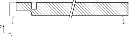
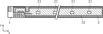
図1〜図4は、本発明の第1実施形態に基づく液晶表示装置バックライト用のLED光源装置を示している。本実施形態のLED光源装置A1は、基板1、ガラス層2、金属膜3、複数のLEDチップ4、リフレクタ51、および透光樹脂55を備えている。LED光源装置A1は、図8および図9に示すように、たとえば液晶表示装置B1のバックライトを構成する光源として用いられる。なお、理解の便宜上、図1においてはガラス層2および透光樹脂55を省略しており、図2においては、透光樹脂55を省略している。
1 to 4 show an LED light source device for a liquid crystal display backlight according to a first embodiment of the present invention. The LED light source device A1 of this embodiment includes a
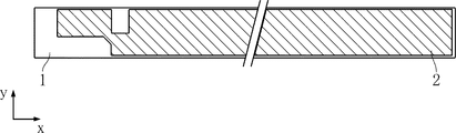
基板1は、たとえばアルミナなどのセラミックスからなり、x方向を長手方向、y方向を幅方向とする長矩形状とされている。本実施形態の基板1は、長さが222mm程度、幅が6.0mm程度、厚さが1.0mm程度とされている。
The
ガラス層2は、金属膜3を形成するのに適した平滑な面を提供するためのものであり、基板1の主面11に形成されている。ガラス層2の厚さは、たとえば100μm程度である。図5は、LED光源装置A1の製造工程において、基板1にガラス層2を形成した状態を示している。ガラス層2の形成は、たとえばガラスペーストを印刷した後に、このガラスペーストを焼成することによって行う。
The
同図に示すように、ガラス層2には、複数の窓部21が形成されている。複数の窓部21は、それぞれが矩形状であり、x方向にほぼ等ピッチで配列されている。窓部21は、x方向寸法が1.8mm程度、y方向寸法が1.2mm程度とされている。また、図3および図4に示すように、ガラス層2には、傾斜面22が形成されている。傾斜面22は、窓部21の外縁につながっており、x方向またはy方向において窓部21から遠ざかるほど、z方向図中上方に位置する傾斜とされている。本実施形態においては、傾斜面22は、z方向視において矩形の枠状とされている。
As shown in the figure, a plurality of
金属膜3は、LEDチップ4への給電機能を果たすものであり、窓部21に重なる部分を除き、ガラス層2上に形成されている。本実施形態においては、金属膜3は、Al層31およびAgPt層32からなる。図6は、LED光源装置A1の製造工程において、AgPt層32を形成した状態を示している。AgPt層32の形成は、たとえばAgおよびPtを含むペーストを印刷した後に、このペーストを焼成することによって行う。AgPt層の厚さは、たとえば10μm程度である。
The
Al層31は、金属膜3の最外層を構成するものである。図7は、LED光源装置A1の製造工程においてAl層31を形成した状態を示している。Al層31の形成は、たとえばスパッタ法を用いて行う。Al層31の厚さは、たとえば1.2μm程度である。Al層31とガラス層2との間には、部分的にAgPt層が介在している。
The
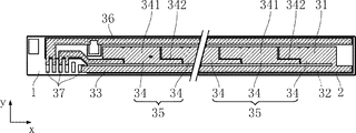
図1〜図4に示すように、金属膜3は、共通帯状部33、複数のアイランド群35、連絡帯状部36、および複数の接続端子部37を有している。図1に示すように、共通帯状部33は、x方向に長く延びる帯状であり、基板1のほぼ全長にわたって形成されている。共通帯状部33の幅は、たとえば1mm程度である。共通帯状部33は、y方向において、基板1の一端寄りに位置している。図4、図6、および図7から理解されるように、本実施形態においては、共通帯状部33は、Al層31とAgPt層32とが積層された構造となっている。
As shown in FIGS. 1 to 4, the
図1に示すように、複数のアイランド群35は、x方向に並べて配置されており、本実施形態においては、2つのアイランド群35が設けられている。各アイランド群35は、複数のアイランド部34によって構成されている。複数のアイランド部34は、共通帯状部33と平行に、x方向に配列されている。本実施形態においては、各アイランド群35が、12個のアイランド部34を含んでいる。図3、図4、図6、および図7から理解されるように、本実施形態においては、アイランド部34は、Al層31のみの単層構造とされている。
As shown in FIG. 1, the plurality of
図2に示すように、アイランド部34は、本体部341と延出部342を有している。本体部341は、x方向を長手方向とし、一部が欠落した矩形状とされている。本実施形態においては、本体部341は、x方向寸法が9.0mm程度、y方向寸法が2.5mm程度である。図2〜図4に示すように、本体部341は、ガラス層2の窓部21および傾斜面22を覆うように形成されている。本体部341のうち窓部21を覆う部分には、LEDチップ4が実装されており、本体部341のうち窓部21に隣接するガラス層2の部分を覆う部分には、ツェナーダイオード41が実装されている。延出部342は、本体部341からx方向に長く延びる部分であり、本実施形態においては、幅が0.5mm程度、長さが3.0mm程度とされている。図2に示すように、あるアイランド部34の延出部342は、x方向左方に隣接するアイランド部34の本体部341の欠落部分にはまり込むように配置されている。
As shown in FIG. 2, the
連絡帯状部36は、x方向に長く延びる帯状であり、基板1のほぼ全長にわたって形成されている。連絡帯状部36の幅は、たとえば1mm程度である。連絡帯状部36は、y方向において、アイランド群35を挟んで共通帯状部33とは反対側の基板1の一端寄りに位置している。図4、図6、および図7から理解されるように、本実施形態においては、共通帯状部33は、Al層31とAgPt層32とが積層された構造となっている。
The connecting
図1に示すように、複数の接続端子部37は、基板1のx方向一端寄りに形成されており、たとえば液晶表示装置B1の電源もしくは制御部(いずれも図示略)と接続するために用いられる。図6および図7から理解されるように、接続端子部37は、AgPt層32によって構成されている。
As shown in FIG. 1, the plurality of
図1においてx方向右方に位置する接続端子部37は、共通帯状部33につながっており、x方向左方に位置する接続端子部37は、連絡帯状部36につながっている。x方向中央に位置する接続端子部37は、複数のアイランド部34のうちx方向においてもっとも左に位置するもの(接続端子部37にもっとも近いもの)につながっている。また、各アイランド群35に含まれる複数のアイランド部34のうちx方向右端に位置するもの(接続端子部37からもっとも遠いもの)は、共通帯状部33につながっている。また、x方向右方(接続端子部37に対して遠い方)に位置するアイランド群35に含まれる複数のアイランド部34のうちx方向左端に位置するもの(接続端子部37からもっとも近いもの)は、連絡帯状部36につながっている。
In FIG. 1, the
LEDチップ4は、たとえばSiからなるサブマウント基板44とGaNからなるn型半導体層、活性層およびp型半導体層が積層された半導体層43とを有する構造とされており、たとえば青色光を発する。半導体層43には、サブマウント基板44側に形成された電極パッド(図示略)が形成されている。これらの電極パッドが、サブマウント基板44に形成された配線パターン(図示略)に接合されている。図2に示すように、LEDチップ4は、アイランド部34の本体部341のうち窓部21を覆う部分に実装されている。これにより、z方向視において、LEDチップ4は、窓部21に内包されており、枠状の傾斜面22に囲まれている。LEDチップ4には、2つの電極が形成されており、一方の電極は、ワイヤ42によって実装されたアイランド部34の本体部341に接続されている。他方の電極は、ワイヤ42によって隣接するアイランド部34の延出部342に接続されている。本実施形態のLEDチップ4は、x方向寸法が1.9mm程度、y方向寸法が1.3mm程度とされている。サブマウント基板44をアイランド部34に接合することにより、LEDチップ4から金属膜3への放熱を高める効果が期待できる。LEDチップ4とアイランド部34との接合は、たとえばAgペースト、エポキシ樹脂、あるいは高伝導率を有する材料からなるフィラーが混入されたエポキシ樹脂を用いれば、放熱効果の促進に好ましい。なお、本実施形態のLEDチップ4は、いわゆる2ワイヤタイプであるが、これと異なり、1本のワイヤ42によって実装可能であるいわゆる1ワイヤタイプのLEDチップ4や、ワイヤ42を用いない実装が可能であるいわゆるフリップチップタイプのLEDチップ4を用いてもよい。
The
上述した金属膜3の構成と、LEDチップ4の実装形態により、本実施形態においては、LED光源装置A1には、互いに直列に接続された12個のLEDチップ4からなるLEDチップ4のグループが2つ含まれており、これらのLEDチップ4のグループどうしが互いに並列に接続された回路を構成している。
Due to the configuration of the
ツェナーダイオード41は、LEDチップ4に過大な逆電圧が印加されるのを防止するためのものであり、アイランド部34の本体部341のうち窓部21を覆う部分に隣接する部分に実装されている。ツェナーダイオード41は、ワイヤ42によって隣接するアイランド部34の延出部342に接続されている。なお、LEDチップ4のサブマウント基板44にツェナーダイオード41と同等の機能を果たす素子を作りこんでもよい。
The
リフレクタ51は、LEDチップ4からの光をより多くz方向へと進行させるためのものであり、たとえば白色樹脂からなる矩形枠状である。リフレクタ51を形成するときには、LEDチップ4の実装が完了している。このため、リフレクタ51は、たとえば利府ロー炉において高温にさらされることがない。これにより、この白色樹脂としては、ポリブチレンテレフタレート(PBT)樹脂を用いることができる。PBT樹脂は、リフレクタ51の表面の反射率を高めるのに適している。リフレクタ51は、LEDチップ4およびツェナーダイオード41を囲むように金属膜3上(一部は、ガラス層2上)に形成されている。本実施形態においては、リフレクタ51は、x方向寸法が6.8mm程度、y方向寸法が3.0mm程度、z方向高さが1mm程度とされている。また、リフレクタ51のうちLEDチップ4を収容する開口部分のサイズは、x方向寸法が3.9mm程度、y方向寸法が1.9mm程度とされている。
The
透光樹脂55は、図3および図4に示すように、リフレクタ51によって囲まれた空間に充填されており、LEDチップ4およびツェナーダイオード41を覆っている。透光樹脂55は、たとえば透明なエポキシ樹脂に蛍光材料が混入された材質からなる。この蛍光材料は、たとえばLEDチップ4からの青色光によって励起されることにより黄色光を発する。LEDチップ4からの青色光と上記蛍光材料からの黄色光とが混色することにより、LED光源装置A1からは白色光が発せられる。なお、上記蛍光材料に代えて、青色光によって励起されることにより赤色光を発する蛍光材料と緑色光を発する蛍光材料とを合わせて用いてもよい。
As shown in FIGS. 3 and 4, the
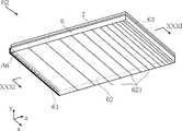
図8および図9は、LED光源装置A1を用いた液晶表示装置の一例を示している。同図に示された液晶表示装置B1は、LED光源装置A1、導光板6、および液晶パネル7を備えている。
8 and 9 show an example of a liquid crystal display device using the LED light source device A1. The liquid crystal display device B1 shown in the figure includes an LED light source device A1, a light guide plate 6, and a
導光板6は、LED光源装置A1とともにバックライトを構成するものであり、たとえば透明なポリカーボネイト樹脂やアクリル樹脂からなる。導光板6は、zx平面に広がる板状とされている。導光板6は、入射面61、反射面62、および出射面63を有している。入射面61は、z方向に対してな平滑な面であり、LED光源装置A1と正対している。反射面62は、y方向に対して直角な面であり、複数の溝621が形成されている。出射面63は、y方向に対して直角な平滑な面であり、反射面とは反対側に位置している。
The light guide plate 6 constitutes a backlight together with the LED light source device A1, and is made of, for example, transparent polycarbonate resin or acrylic resin. The light guide plate 6 has a plate shape extending in the zx plane. The light guide plate 6 has an
図9に示すように、LED光源装置A1から出射された光は、入射面61から入射したのちに、導光板6内を進行する。進行してきた光は、反射面62の溝621によって反射あるいは拡散されることにより、y方向に向けて進行する。反射面62から進行してきた光は、出射面63から出射する。これにより、LED光源装置A1が発光すると、導光板6の出射面63前面から白色光が発せられる。
As shown in FIG. 9, the light emitted from the LED light source device A <b> 1 travels through the light guide plate 6 after entering from the
液晶パネル7は、導光板6から出射された光を選択的に透過させることにより液晶表示装置B1が表示するべき画像を形成するためのものである。液晶パネル7は、たとえば対抗する2枚の透明基板とこれらの透明基板に挟まれた液晶層とからなり、たとえばアクティブマトリクス方式によって、画素ごとに透過状態を変更可能に構成されている。
The
次に、LED光源装置A1および液晶表示装置B1の作用について説明する。 Next, the operation of the LED light source device A1 and the liquid crystal display device B1 will be described.
本実施形態によれば、LEDチップ4からの光のうち金属膜3に向けて発せられた光は、金属膜3によって反射される。このため、より多くの光をLED光源装置A1から出射することが可能であり、輝度向上を図ることができる。特に、金属膜3は、最外層がAl層31からなるため、吸収される割合は小さい。これは、LED光源装置A1の輝度向上に有利である。本実施形態においては、金属膜3は、共通帯状部33、複数のアイランド部34、および連絡帯状部36を区画するためのスリットが形成されているほかは、基板1の主面11のほとんどを覆っている。これにより、LEDチップ4からの光が不当に吸収されてしまうことを抑制することができる。
According to the present embodiment, the light emitted from the
金属膜3は、ガラス層2上に形成されている。このため、金属膜3の表面は、鏡面に近い平滑な面となっている。これにより、LEDチップ4からの光をより高い割合で反射することが可能である。スパッタによって形成されたAl層31は、高密度であり、鏡面状態を実現するのに適している。
The
金属膜3(本体部341)のうち傾斜面22を覆う部分は、LEDチップ4を囲む枠状の反射領域を形成している。このため、LEDチップ4からの光をより高い割合で出射することが可能である。印刷および焼成を用いた手法によれば、ガラス層2の傾斜面22を適切に形成することができる。また、リフレクタ51によってもLEDチップ4からの光が吸収されてしまうことを抑制可能である。
A portion of the metal film 3 (main body portion 341) that covers the
LEDチップ4は、z方向視において窓部21に内包されている。これにより、LEDチップ4と基板1との間には、金属膜3が介在するのみであり、ガラス層2は介在していない。これは、LEDチップ4の放熱促進に適している。
The
金属膜3に共通帯状部33、複数のアイランド部34、および連絡帯状部36を備えることにより、複数のLEDチップ4を適切に接続することが可能である。
By providing the
共通帯状部33および連絡帯状部36をAl層31とAgPt層32の積層構造とすることにより、抵抗値を低下させることが可能である。共通帯状部33および連絡帯状部36は、比較的狭幅であり、かつ長さが長いため、電圧低下が生じやすい。上述した積層構造によれば、共通帯状部33および連絡帯状部36の電圧低下を抑制することができる。
By making the
LED光源装置A1の輝度向上を図ることにより、液晶表示装置B1は、より明るく、より鮮明な画像を表示することができる。 By improving the luminance of the LED light source device A1, the liquid crystal display device B1 can display a brighter and clearer image.
図10〜図20は、本発明の他の実施形態を示している。なお、これらの図において、上記実施形態と同一または類似の要素には、上記実施形態と同一の符号を付している。 10 to 20 show another embodiment of the present invention. In these drawings, the same or similar elements as those in the above embodiment are denoted by the same reference numerals as those in the above embodiment.
図10および図11は、本発明の第2実施形態に基づくLED光源装置を示している。本実施形態のLED光源装置A2は、金属膜3の構成が上述した実施形態と異なっている。本実施形態においては、金属膜3は、AgPt層32のみからなる。AgPt層32は、明るい白色を呈するものであり、比較的反射率が高い。したがって、このような構成によってもLED光源装置A2の輝度向上を図ることができる。また、LED光源装置A2を製造する際には、Al層31を形成する工程を省略可能である。これにより、LED光源装置A2のコスト低減を図ることができる。
10 and 11 show an LED light source device according to the second embodiment of the present invention. The LED light source device A2 of the present embodiment is different from the above-described embodiment in the configuration of the
図12および図13は、本発明の第3実施形態に基づくLED光源装置を示している。本実施形態のLED光源装置A3は、ガラス層2に窓部21および傾斜面22が形成されていない点が上述した実施形態と異なっている。このような実施形態においては、本体部341の全面が鏡面状態となる。これによって、LEDチップ4からの光がz方向へと反射する割合を高めるという効果が期待できる。
12 and 13 show an LED light source device according to a third embodiment of the present invention. The LED light source device A3 of this embodiment is different from the above-described embodiment in that the
図14および図15は、本発明の第4実施形態に基づくLED光源装置を示している。本実施形態のLED光源装置A4は、ガラス層2を備えない点が上述した実施形態と異なっている。ガラス層2を備えない場合、金属膜3の表面は、艶消し状態の白色面となる。このような状態の金属膜3であっても、最外層がAl層31からなるため、反射率は相対的に高い。したがって、LED光源装置A4の輝度向上を図ることができる。また、ガラス層2を形成する工程を省略可能であるため、LED光源装置A4のコスト低減に有利である。また、LEDチップ4からの放熱促進を図ることができる。
14 and 15 show an LED light source device according to a fourth embodiment of the present invention. The LED light source device A4 of this embodiment is different from the above-described embodiment in that the
図16および図17は、本発明の第5実施形態に基づくLED光源装置を示している。本実施形態のLED光源装置A5は、リフレクタ51を備えない点が上述した実施形態と異なっている。本実施形態においては、透光樹脂55は、たとえば液体樹脂材料をポッティングによってLEDチップ4を覆うように滴下したのちに、この液体樹脂材料を硬化させることによって形成する。このような実施形態によっても、基板1の主面11のほとんどが金属膜3によって覆われているため、LEDチップ4からの光が不当に吸収されてしまうことを抑制可能であり、LED光源装置A5の輝度向上を図ることができる。
16 and 17 show an LED light source device according to a fifth embodiment of the present invention. The LED light source device A5 of the present embodiment is different from the above-described embodiment in that the
図18は、本発明の第1実施形態に基づくLED光源装置と、これの変形例とを組み合わせた構成を示している。同図に示されたLED光源装置A1’は、上述したLED光源装置A1と比較して、接続端子部37が省略されている点が異なっている。LED光源装置A1とLED光源装置A1’の共通帯状部33どうし、および連絡帯状部36どうしが、それぞれ配線38によって接続されている。このような構成により、より大きな画面サイズの液晶表示装置のバックライト用LED光源装置を実現することができる。
FIG. 18 shows a configuration in which the LED light source device according to the first embodiment of the present invention and a modification thereof are combined. The LED light source device A1 'shown in the figure is different from the LED light source device A1 described above in that the
図19および図20は、LED光源装置A1において、異なる種類のLEDチップ4が適用された構成を示している。以下に説明するLEDチップ4は、LED光源装置A1のみならず、LED光源装置A2〜A5、およびLED光源装置A1’に用いることができることはもちろんである。
19 and 20 show a configuration in which different types of
図19に示されたLED光源装置A1に用いられたLEDチップ4は、いわゆる2ワイヤタイプと称される構造を有する。具体的には、下層からn型半導体層、活性層、およびp型半導体層が積層された半導体層43によって構成されており、n型半導体層およびp型半導体層に導通する2つの電極パッド(図示略)が図中上面に配置されている。これらの電極パッドに、ワイヤ42がボンディングされている。
The
図20に示されたLEDチップ4は、ワイヤ42を用いることなく実装可能なタイプである。具体的には、サブマウント基板44に2つのスルーホール電極441が形成されている。これらのスルーホール電極441は、サブマウント基板44に形成された配線パターンを介して、半導体層43のn型半導体層およびp型半導体層にそれぞれ導通している。スルーホール電極441の下面には、実装用のバンプ442が形成されている。LEDチップ4は、このバンプ442によって、金属膜3に実装されている。
The
本発明に係る液晶表示装置バックライト用LED光源装置および液晶表示装置は、上述した実施形態に限定されるものではない。本発明に係る液晶表示装置バックライト用LED光源装置および液晶表示装置の各部の具体的な構成は、種々に設計変更自在である。 The LED light source device for a liquid crystal display device backlight and the liquid crystal display device according to the present invention are not limited to the above-described embodiments. The specific configuration of each part of the liquid crystal display backlight LED light source device and the liquid crystal display device according to the present invention can be varied in design in various ways.
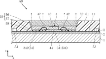
図21〜図25は、本発明の第6実施形態に基づく液晶表示装置バックライト用のLED光源装置を示している。本実施形態のLED光源装置A6は、基板1、ガラス層2、金属膜3、複数のLEDチップ4、リフレクタ51、透光樹脂55、および白色樹脂58を備えている。LED光源装置A6は、図30および図31に示すように、たとえば液晶表示装置B2のバックライトを構成する光源として用いられる。なお、理解の便宜上、図21および図22においてはガラス層2、および透光樹脂55を省略しており、図23においては、透光樹脂55を省略している。
21 to 25 show an LED light source device for a liquid crystal display backlight according to a sixth embodiment of the present invention. The LED light source device A6 of this embodiment includes a
基板1は、たとえばアルミナなどのセラミックスからなり、x方向を長手方向、y方向を幅方向とする長矩形状とされている。本実施形態の基板1は、長さが222mm程度、幅が6.0mm程度、厚さが1.0mm程度とされている。
The
ガラス層2は、金属膜3を形成するのに適した平滑な面を提供するためのものであり、基板1の主面11に形成されている。ガラス層2の厚さは、たとえば100μm程度である。図26は、LED光源装置A6の製造工程において、基板1にガラス層2を形成した状態を示している。ガラス層2の形成は、たとえばガラスペーストを印刷した後に、このガラスペーストを焼成することによって行う。
The
金属膜3は、LEDチップ4への給電機能を果たすものであり、ガラス層2上に形成されている。本実施形態においては、金属膜3は、Al層31およびAgPt層32からなる。図27は、LED光源装置A6の製造工程において、AgPt層32を形成した状態を示している。AgPt層32の形成は、たとえばAgおよびPtを含むペーストを印刷した後に、このペーストを焼成することによって行う。AgPt層32の厚さは、たとえば10μm程度である。
The
Al層31は、金属膜3の最外層を構成するものである。図28は、LED光源装置A6の製造工程においてAl層31を形成した状態を示している。Al層31の形成は、たとえばスパッタ法を用いて行う。Al層31の厚さは、たとえば1.2μm程度である。Al層31とガラス層2との間には、部分的にAgPt層32が介在している。
The
図22〜図25に示すように、金属膜3は、共通帯状部33、複数のアイランド群35、連絡帯状部36、および複数の接続端子部37を有している。図22に示すように、共通帯状部33は、x方向に長く延びる帯状であり、基板1のほぼ全長にわたって形成されている。共通帯状部33の幅は、たとえば1mm程度である。共通帯状部33は、y方向において、基板1の一端寄りに位置している。図25、図27、および図28から理解されるように、本実施形態においては、共通帯状部33は、Al層31とAgPt層32とが積層された構造となっている。
As shown in FIGS. 22 to 25, the
図22に示すように、複数のアイランド群35は、x方向に並べて配置されており、本実施形態においては、2つのアイランド群35が設けられている。各アイランド群35は、複数のアイランド部34によって構成されている。複数のアイランド部34は、共通帯状部33と平行に、x方向に配列されている。本実施形態においては、各アイランド群35が、12個のアイランド部34を含んでいる。図24、図25、図27、および図28から理解されるように、本実施形態においては、アイランド部34は、Al層31のみの単層構造とされている。
As shown in FIG. 22, the plurality of
図23および図24に示すように、アイランド部34は、本体部341と延出部342を有している。本体部341は、x方向を長手方向とし、一部が欠落した矩形状とされている。本実施形態においては、本体部341は、x方向寸法が9.0mm程度、y方向寸法が2.5mm程度である。本体部341には、LEDチップ4が実装されている。延出部342は、本体部341からx方向に長く延びる部分であり、本実施形態においては、幅が0.5mm程度、長さが3.0mm程度とされている。図23に示すように、あるアイランド部34の延出部342は、x方向右方に隣接するアイランド部34の本体部341の欠落部分にはまり込むように配置されている。
As shown in FIGS. 23 and 24, the
連絡帯状部36は、x方向に長く延びる帯状であり、基板1のほぼ全長にわたって形成されている。連絡帯状部36の幅は、たとえば1mm程度である。連絡帯状部36は、y方向において、アイランド群35を挟んで共通帯状部33とは反対側の基板1の一端寄りに位置している。図25、図27、および図28から理解されるように、本実施形態においては、共通帯状部33は、Al層31とAgPt層32とが積層された構造となっている。
The connecting
図22に示すように、複数の接続端子部37は、基板1のx方向一端寄りに形成されており、たとえば液晶表示装置B2の電源もしくは制御部(いずれも図示略)と接続するために用いられる。図27および図28から理解されるように、接続端子部37は、AgPt層32によって構成されている。
As shown in FIG. 22, the plurality of
図22においてx方向右方に位置する接続端子部37は、共通帯状部33につながっており、x方向左方に位置する接続端子部37は、連絡帯状部36につながっている。x方向中央に位置する接続端子部37は、複数のアイランド部34のうちx方向においてもっとも左に位置するもの(接続端子部37にもっとも近いもの)につながっている。また、各アイランド群35に含まれる複数のアイランド部34のうちx方向右端に位置するもの(接続端子部37からもっとも遠いもの)は、共通帯状部33につながっている。また、x方向右方(接続端子部37に対して遠い方)に位置するアイランド群35に含まれる複数のアイランド部34のうちx方向左端に位置するもの(接続端子部37からもっとも近いもの)は、連絡帯状部36につながっている。
In FIG. 22, the
LEDチップ4は、Siからなるサブマウント基板44とたとえばGaNからなるn型半導体層、活性層およびp型半導体層が積層された半導体層43とを有する構造とされており、たとえば青色光を発する。半導体層43には、サブマウント基板44側に形成された電極パッド(図示略)が形成されている。これらの電極パッドが、サブマウント基板44に形成された配線パターン(図示略)に接合されている。サブマウント基板44には、ツェナーダイオードが作りこまれている。このツェナーダイオードは、半導体層43に過大な逆電圧が印加されることを回避するためのものである。
The
図23に示すように、LEDチップ4は、アイランド部34に実装されている。LEDチップ4には、2つの電極が形成されており、一方の電極は、ワイヤ42によって実装されたアイランド部34の本体部341に接続されている。他方の電極は、ワイヤ42によって隣接するアイランド部34の延出部342に接続されている。本実施形態のLEDチップ4は、x方向寸法が1.9mm程度、y方向寸法が1.3mm程度とされている。サブマウント基板44をアイランド部34に接合することにより、LEDチップ4から金属膜3への放熱を高める効果が期待できる。LEDチップ4とアイランド部34との接合は、たとえばAgペースト、エポキシ樹脂、あるいは高熱伝導率を有する材料からなるフィラーが混入されたエポキシ樹脂を用いれば、放熱効果の促進に好ましい。
As shown in FIG. 23, the
上述した金属膜3の構成と、LEDチップ4の実装形態により、本実施形態においては、LED光源装置A6には、互いに直列に接続された12個のLEDチップ4からなるLEDチップ4のグループが2つ含まれており、これらのLEDチップ4のグループどうしが互いに並列に接続された回路を構成している。
According to the configuration of the
リフレクタ51は、LEDチップ4からの光をより多くz方向へと進行させるためのものであり、たとえば液晶ポリマまたはポリブチレンテレフタレートなどの白色樹脂からなる。リフレクタ51は、x方向に長く延びた形状であり、複数の開口52および複数の凹部53が形成されている。各開口52は、z方向視において矩形状とされている。図24および図25に示すように開口52の内面は、各LEDチップ4を囲んでおり、主面11の法線方向において基板1から遠ざかるほどLEDチップ4から遠くなるように傾斜している。各凹部53は、図22〜図24に示すように、隣り合う開口52の間に位置している。各凹部53は、リフレクタ51の上面から凹む断面矩形状の溝である。リフレクタ51のうち凹部53が形成された部位は、yz平面における断面積が部分的に縮小しており、本発明で言う小断面部に相当する。本実施形態においては、リフレクタ51のy方向寸法が2.0〜4.0mm程度とされている。
The
LED光源装置A6の製造工程においては、図29に示すように、リフレクタ51は、LEDチップ4の実装が完了した基板1に対して貼りつけられる。本実施形態においては、リフレクタ51は、y方向寸法が3.0mm程度、z方向高さが1mm程度とされている。また、開口52のサイズは、x方向寸法が3.9mm程度、y方向寸法が1.9mm程度とされている。凹部53は、x方向寸法が0.5〜4.0mm程度、z方向深さが0.2〜0.8mm程度とされている。
In the manufacturing process of the LED light source device A6, as shown in FIG. 29, the
白色樹脂58は、本発明で言う不透明樹脂の一例に相当し、たとえば白色のエポキシ樹脂などLEDチップ4からの光に対して不透明であり、かつサブマウント基板44よりも高反射率である材質からなる。図23〜図25に示すように、白色樹脂58は、リフレクタ51の開口52に囲まれた領域のうち、LEDチップ4を除く部分を覆っている。また、白色樹脂58は、サブマウント基板44の側面をすべて覆っている。なお、本実施形態とは異なり、サブマウント基板44の側面の一部が白色樹脂58に覆われている構成であってもよい。
The
透光樹脂55は、図24および図25に示すように、開口52内に充填されており、LEDチップ4を覆っている。透光樹脂55は、透明部57と蛍光部56とからなる。透明部57は、白色樹脂58上に積層されており、本実施形態においては、半導体層43を覆っている。透明部57は、たとえば透明なエポキシ樹脂またはシリコーン樹脂からなる。蛍光部56は、透明部57上に積層されており、たとえば透明なエポキシ樹脂に蛍光材料が混入された材質からなる。この蛍光材料は、たとえばLEDチップ4からの青色光によって励起されることにより黄色光を発する。LEDチップ4からの青色光と上記蛍光材料からの黄色光とが混色することにより、LED光源装置A6からは白色光が発せられる。なお、上記蛍光材料に代えて、青色光によって励起されることにより赤色光を発する蛍光材料と緑色光を発する蛍光材料とを合わせて用いてもよい。
As shown in FIGS. 24 and 25, the
図30および図31は、LED光源装置A6を用いた液晶表示装置の一例を示している。同図に示された液晶表示装置B2は、LED光源装置A6、導光板6、および液晶パネル7を備えている。
30 and 31 show an example of a liquid crystal display device using the LED light source device A6. The liquid crystal display device B2 shown in the figure includes an LED light source device A6, a light guide plate 6, and a
導光板6は、LED光源装置A6とともにバックライトを構成するものであり、たとえば透明なポリカーボネイト樹脂やアクリル樹脂からなる。導光板6は、zx平面に広がる板状とされている。導光板6は、入射面61、反射面62、および出射面63を有している。入射面61は、z方向に対して平滑な面であり、LED光源装置A6と正対している。反射面62は、y方向に対して直角な面であり、複数の溝621が形成されている。出射面63は、y方向に対して直角な平滑な面であり、反射面62とは反対側に位置している。
The light guide plate 6 constitutes a backlight together with the LED light source device A6, and is made of, for example, transparent polycarbonate resin or acrylic resin. The light guide plate 6 has a plate shape extending in the zx plane. The light guide plate 6 has an
図31に示すように、LED光源装置A6から出射された光は、入射面61から入射したのちに、導光板6内を進行する。進行してきた光は、反射面62の溝621によって反射あるいは拡散されることにより、y方向に向けて進行する。反射面62から進行してきた光は、出射面63から出射する。これにより、LED光源装置A6が発光すると、導光板6の出射面63全面から白色光が発せられる。
As shown in FIG. 31, the light emitted from the LED light source device A <b> 6 proceeds through the light guide plate 6 after entering from the
液晶パネル7は、導光板6から出射された光を選択的に透過させることにより液晶表示装置B2が表示するべき画像を形成するためのものである。液晶パネル7は、たとえば対向する2枚の透明基板とこれらの透明基板に挟まれた液晶層とからなり、たとえばアクティブマトリクス方式によって、画素ごとに透過状態を変更可能に構成されている。
The
次に、LED光源装置A6および液晶表示装置B2の作用について説明する。 Next, the operation of the LED light source device A6 and the liquid crystal display device B2 will be described.
各LEDチップ4がリフレクタ51の開口52に囲まれていることにより、LEDチップ4から側方に進行した光は、開口52によって反射される。開口52の内面は、図24および図25に示すように、上方に向けて開くように傾斜している。このため、反射された光は、LED光源装置A6外へと出射されやすい。したがって、LED光源装置A6の高輝度化を図ることができる。
Since each
さらに、図29に示すように、リフレクタ51を形成するときには、LEDチップ4の実装が完了している。このため、リフレクタ51は、たとえばLEDチップ4を実装する工程において用いられるリフロー炉において高温にさらされることがない。これにより、この白色樹脂としては、液晶ポリマまたはポリブチレンテレフタレートを用いることができる。液晶ポリマまたはポリブチレンテレフタレートは、リフレクタ51の表面の反射率を高めるのに適している。これは、LED光源装置A6の高輝度化に有利である。
Furthermore, as shown in FIG. 29, when the
図29に示すように、リフレクタ51は、基板1に取り付けられる前においては、それ単独で取り扱われることが多い。リフレクタ51の保持方法によっては、リフレクタ51に過大なモーメントが作用しうる。複数の凹部53が形成された複数の小断面部は、これら以外の部位よりも弾性変形しやすい。したがって、リフレクタ51にモーメントが作用したときには、上記複数の小断面部が積極的に変形することにより、リフレクタ51のいずれかの部分に亀裂が入ることなどを防止することができる。
As shown in FIG. 29, the
凹部53は、リフレクタ51のうち基板1とは反対側の面から凹むように形成されている。これにより、リフレクタ51のうち基板1と接合されている面積は、上記小断面部を設けることによっては縮小されていない。したがって、リフレクタ51の保護を図りつつ、リフレクタ51と基板1との接合力低下を回避することができる。
The
本実施形態によれば、白色樹脂58は、LEDチップ4のサブマウント基板44の側面を覆っている。サブマウント基板44の材質であるSiは、比較的光を吸収しやすい。白色樹脂58は、サブマウント基板44の側面によって半導体層43からの光が吸収されることを防ぐ働きを果たす。これにより、LED光源装置A6の高輝度化をさらに促進することができる。
According to the present embodiment, the
また、白色樹脂58は、開口52によって囲まれた領域のうちLEDチップ4を除く部分すべてを覆っている。このため、基板1などによって半導体層43からの光が吸収されてしまうことを回避することが可能である。これは、LED光源装置A6の高輝度化に有利である。
Further, the
LEDチップ4は、サブマウント基板44に作りこまれたツェナーダイオードを有している。このツェナーダイオードにより、半導体層43に過大な逆電圧が印加されることを防止することができる。また、このツェナーダイオードを設けることによってLED光源装置A6の高輝度化が阻害されることはない。
The
透光樹脂55に透明部57を設けることにより、透光樹脂55に含まれる蛍光材料の量を削減することができる。これは、LED光源装置A6の低コスト化に有利である。
By providing the
LED光源装置A6の輝度向上を図ることにより、液晶表示装置B2は、より明るく、より鮮明な画像を表示することができる。 By improving the luminance of the LED light source device A6, the liquid crystal display device B2 can display a brighter and clearer image.
図32〜図49は、本発明の他の実施形態を示している。なお、これらの図において、上記実施形態と同一または類似の要素には、上記実施形態と同一の符号を付している。 32 to 49 show another embodiment of the present invention. In these drawings, the same or similar elements as those in the above embodiment are denoted by the same reference numerals as those in the above embodiment.
図32は、LED光源装置A6の凹部53についての変形例を示している。本変形例のLED光源装置A6は、凹部53の構成が上述したLED光源装置A6と異なっている。本変形例においては、リフレクタ51のy方向を向く側面から凹むように、複数の凹部53が形成されている。より具体的には、隣り合う開口52の間に1対の凹部53が配置されている。1対の凹部53は、リフレクタ51のy方向両側に形成されている。このような変形例によっても、LED光源装置A6の高輝度化を図りつつ、リフレクタ51に亀裂が生じることなどを防止することができる。
FIG. 32 shows a modification of the
図33は、LED光源装置A6の凹部53についての他の変形例を示している。本変形例のLED光源装置A6は、凹部53の構成が上述したLED光源装置A6と異なっている。本変形例においては、リフレクタ51の基板1に接合された面から凹むように、複数の凹部53が形成されている。各凹部53は、隣り合う開口52の間に配置されている。このような変形例によっても、LED光源装置A6の高輝度化を図りつつ、リフレクタ51に亀裂が生じることなどを防止することができる。
FIG. 33 shows another modification of the
図34および図35は、LED光源装置A6の金属膜3についての変形例を示している。本変形例においては、金属膜3は、AgPt層32のみからなる。このような変形例によれば、LED光源装置A6を製造する際には、Al層31を形成する工程を省略可能である。これにより、LED光源装置A6のコスト低減を図ることができる。
34 and 35 show a modification of the
図36および図37は、LED光源装置A6の他の変形例を示している。本変形例においては、ガラス層2を備えない点が上述したLED光源装置A6と異なっている。このような変形例によれば、ガラス層2を形成する工程を省略可能であるため、LED光源装置A6のコスト低減に有利である。また、LEDチップ4からの放熱促進を図ることができる。
36 and 37 show another modification of the LED light source device A6. The present modification is different from the LED light source device A6 described above in that the
図38は、LED光源装置A6のLEDチップ4についての変形例を示している。本変形例のLEDチップ4は、ワイヤ42を用いることなく実装可能なタイプである。具体的には、サブマウント基板44に2つのスルーホール電極441が形成されている。これらのスルーホール電極441は、サブマウント基板44に形成された配線パターンを介して、半導体層43のn型半導体層およびp型半導体層にそれぞれ導通している。スルーホール電極441の下面には、実装用のバンプ442が形成されている。LEDチップ4は、このバンプ442によって、金属膜3に実装されている。
FIG. 38 shows a modification of the
図39は、LED光源装置A6の透光樹脂55についての変形例を示している。本変形例においては、透光樹脂55が蛍光部56のみによって構成されている。このような変形例によっても、LED光源装置A6の高輝度化を図ることができる。
FIG. 39 shows a modification of the
図40は、LED光源装置A6の変形例を示している。本変形例は、LEDチップ4とは別体とされたツェナーダイオード41を備えている。ツェナーダイオード41は、LEDチップ4とともにアイランド部34の本体部341に実装されている。ツェナーダイオード41は、LEDチップ4の半導体層43に過大な逆電圧が印加されることを防止する。また、ツェナーダイオード41は、白色樹脂58によって覆われている。これにより、LEDチップ4からの光がツェナーダイオード41によって吸収されることを防止することができる。
FIG. 40 shows a modification of the LED light source device A6. This modification includes a
図41は、本発明の第6実施形態に基づくLED光源装置と、これの変形例とを組み合わせた構成を示している。同図に示されたLED光源装置A6’は、上述したLED光源装置A6と比較して、接続端子部37が省略されている点が異なっている。LED光源装置A6とLED光源装置A6’の共通帯状部33どうし、および連絡帯状部36どうしが、それぞれ配線38によって接続されている。このような構成により、より大きな画面サイズの液晶表示装置のバックライト用LED光源装置を実現することができる。
FIG. 41 shows a configuration in which the LED light source device according to the sixth embodiment of the present invention and a modification thereof are combined. The LED light source device A6 'shown in the figure is different from the LED light source device A6 described above in that the
図42〜図44は、本発明の第7実施形態に基づくLED光源装置A7を示している。本実施形態のLED光源装置A7は、白色樹脂58を備えない点と、ガラス層2および金属膜3の構成とが、上述したLED光源装置A6と異なっている。
42 to 44 show an LED light source device A7 according to the seventh embodiment of the present invention. The LED light source device A7 of this embodiment is different from the LED light source device A6 described above in that the
ガラス層2には、複数の窓部21が形成されている。複数の窓部21は、それぞれが矩形状であり、x方向にほぼ等ピッチで配列されている。窓部21は、x方向寸法が1.8mm程度、y方向寸法が1.2mm程度とされている。また、図43および図44に示すように、ガラス層2には、傾斜面22が形成されている。傾斜面22は、窓部21の外縁につながっており、x方向またはy方向において窓部21から遠ざかるほど、z方向図中上方に位置する傾斜とされている。本実施形態においては、傾斜面22は、z方向視において矩形の枠状とされている。
A plurality of
本体部341は、ガラス層2の窓部21および傾斜面22を覆うように形成されている。本体部341のうち窓部21を覆う部分には、LEDチップ4が実装されており、本体部341のうち窓部21に隣接するガラス層2を覆う部分には、ツェナーダイオード41が実装されている。アイランド部34は、Al層31のみの単層構造とされている。
The
LEDチップ4は、アイランド部34の本体部341のうち窓部21を覆う部分に実装されている。これにより、z方向視において、LEDチップ4は、窓部21に内包されており、枠状の傾斜面22に囲まれている。
The
LED光源装置A7の製造方法においては、まず、図45に示すように基板1に複数の窓部21を有するガラス層2を形成する。ついで、図46に示すようにAgPt層32を形成する。そして、図47に示すように、窓部21を覆うようにAl層31を形成する。
In the manufacturing method of the LED light source device A7, first, the
本実施形態によれば、LEDチップ4からの光のうち金属膜3に向けて発せられた光は、金属膜3によって反射される。このため、より多くの光をLED光源装置A7から出射することが可能であり、輝度向上を図ることができる。特に、金属膜3は、最外層がAl層31からなるため、吸収される割合は小さい。これは、LED光源装置A7の輝度向上に有利である。本実施形態においては、金属膜3は、共通帯状部33、複数のアイランド部34、および連絡帯状部36を区画するためのスリットが形成されているほかは、基板1の主面11のほとんどを覆っている。これにより、LEDチップ4からの光が不当に吸収されてしまうことを抑制することができる。
According to the present embodiment, the light emitted from the
金属膜3は、ガラス層2上に形成されている。このため、金属膜3の表面は、鏡面に近い平滑な面となっている。これにより、LEDチップ4からの光をより高い割合で反射することが可能である。スパッタによって形成されたAl層31は、高密度であり、鏡面状態を実現するのに適している。
The
金属膜3(本体部341)のうち傾斜面22を覆う部分は、LEDチップ4を囲む枠状の反射領域を形成している。このため、LEDチップ4からの光をより高い割合で出射することが可能である。印刷および焼成を用いた手法によれば、ガラス層2の傾斜面22を適切に形成することができる。また、リフレクタ51によってもLEDチップ4からの光が吸収されてしまうことを抑制可能である。
A portion of the metal film 3 (main body portion 341) that covers the
LEDチップ4は、z方向視において窓部21に内包されている。これにより、LEDチップ4と基板1との間には、金属膜3が介在するのみであり、ガラス層2は介在していない。これは、LEDチップ4の放熱促進に適している。
The
金属膜3に共通帯状部33、複数のアイランド部34、および連絡帯状部36を備えることにより、複数のLEDチップ4を適切に接続することが可能である。
By providing the
共通帯状部33および連絡帯状部36をAl層31とAgPt層32の積層構造とすることにより、抵抗値を低下させることが可能である。共通帯状部33および連絡帯状部36は、比較的狭幅であり、かつ長さが長いため、電圧低下が生じやすい。上述した積層構造によれば、共通帯状部33および連絡帯状部36の電圧低下を抑制することができる。
By making the
なお、金属膜3の構成は、本実施形態の構成に限定されず、たとえば図34〜図37に示した構成を採用できることはもちろんである。
In addition, the structure of the
図48は、LED光源装置A7のLEDチップ4についての変形例を示している。本変形例のLEDチップ4は、いわゆる2ワイヤタイプと称される構造を有する。具体的には、下層からn型半導体層、活性層、およびp型半導体層が積層された半導体層43によって構成されており、n型半導体層およびp型半導体層に導通する2つの電極パッド(図示略)が図中上面に配置されている。これらの電極パッドに、ワイヤ42がボンディングされている。
FIG. 48 shows a modification of the
図49は、本発明の第8実施形態に基づくLED光源装置を示している。本実施形態のLED光源装置A8は、1つの基板1に2つのリフレクタ51が取り付けられている点が、上述したLED光源装置A6と異なっている。本実施形態においては、リフレクタ51は、x方向長さが基板1の半分弱程度とされている。2つのリフレクタ51は、x方向に直列に配置されており、LED光源装置A6と同様に、それぞれに形成された開口52がLEDチップ4を格別に囲んでいる。
FIG. 49 shows an LED light source device according to the eighth embodiment of the present invention. The LED light source device A8 of this embodiment is different from the LED light source device A6 described above in that two
このような実施形態によっても、LED光源装置A6の高輝度化を図ることができる。また、基板1に対してx方向が短いリフレクタ51を用意することにより、基板1の長さに応じて、1枚の基板1に取り付けるリフレクタ51の個数を調整することができる。これにより、異なる長さの複数種類の基板1に対してリフレクタ51を共通部品化することが可能であり、様々な長さのLED光源装置A7を効率よく製造することができる。
Also according to such an embodiment, the brightness of the LED light source device A6 can be increased. In addition, by preparing the
本発明に係る液晶表示装置バックライト用LED光源装置および液晶表示装置は、上述した実施形態に限定されるものではない。本発明に係る液晶表示装置バックライト用LED光源装置および液晶表示装置の各部の具体的な構成は、種々に設計変更自在である。 The LED light source device for a liquid crystal display device backlight and the liquid crystal display device according to the present invention are not limited to the above-described embodiments. The specific configuration of each part of the liquid crystal display backlight LED light source device and the liquid crystal display device according to the present invention can be varied in design in various ways.
図50〜図54は、本発明の第9実施形態に基づく液晶表示装置バックライト用のLED光源装置を示している。本実施形態のLED光源装置A9は、基板1、ガラス層2、金属膜3、複数のLEDチップ4、リフレクタ51、透光樹脂55、および白色樹脂58を備えている。LED光源装置A9は、図59および図60に示すように、たとえば液晶表示装置B3のバックライトを構成する光源として用いられる。なお、理解の便宜上、図50および図51においてはガラス層2、および透光樹脂55を省略しており、図52においては、透光樹脂55を省略している。
50 to 54 show an LED light source device for a liquid crystal display backlight according to a ninth embodiment of the present invention. The LED light source device A9 of this embodiment includes a
基板1は、たとえばアルミナなどのセラミックスからなり、x方向を長手方向、y方向を幅方向とする長矩形状とされている。本実施形態の基板1は、長さが222mm程度、幅が6.0mm程度、厚さが1.0mm程度とされている。基板1は主面11を有する。主面11の法線方向は方向zに一致する。以下、適宜、法線方向zと称する。
The
ガラス層2は、金属膜3を形成するのに適した平滑な面を提供するためのものであり、基板1の主面11に形成されている。ガラス層2の厚さは、たとえば100μm程度である。図55は、LED光源装置A9の製造工程において、基板1にガラス層2を形成した状態を示している。ガラス層2の形成は、たとえばガラスペーストを印刷した後に、このガラスペーストを焼成することによって行う。
The
金属膜3は、LEDチップ4への給電機能を果たすものであり、ガラス層2上に形成されている。本実施形態においては、金属膜3は、Al層31およびAgPt層32からなる。図56は、LED光源装置A9の製造工程において、AgPt層32を形成した状態を示している。AgPt層32の形成は、たとえばAgおよびPtを含むペーストを印刷した後に、このペーストを焼成することによって行う。AgPt層32の厚さは、たとえば10μm程度である。
The
Al層31は、金属膜3の最外層を構成するものである。図57は、LED光源装置A9の製造工程においてAl層31を形成した状態を示している。Al層31の形成は、たとえばスパッタ法を用いて行う。Al層31の厚さは、たとえば1.2μm程度である。Al層31とガラス層2との間には、部分的にAgPt層32が介在している。
The
図51〜図54に示すように、金属膜3は、共通帯状部33、複数のアイランド群35、連絡帯状部36、および複数の接続端子部37を有している。図51に示すように、共通帯状部33は、x方向に長く延びる帯状であり、基板1のほぼ全長にわたって形成されている。共通帯状部33の幅は、たとえば1mm程度である。共通帯状部33は、y方向において、基板1の一端寄りに位置している。図54、図56、および図57から理解されるように、本実施形態においては、共通帯状部33は、Al層31とAgPt層32とが積層された構造となっている。
As shown in FIGS. 51 to 54, the
図51に示すように、複数のアイランド群35は、x方向に並べて配置されており、本実施形態においては、2つのアイランド群35が設けられている。各アイランド群35は、複数のアイランド部34によって構成されている。複数のアイランド部34は、共通帯状部33と平行に、x方向に配列されている。本実施形態においては、各アイランド群35が、12個のアイランド部34を含んでいる。図53、図54、図56、および図57から理解されるように、本実施形態においては、アイランド部34は、Al層31のみの単層構造とされている。
As shown in FIG. 51, the plurality of
図52および図53に示すように、アイランド部34は、本体部341と延出部342を有している。本体部341は、x方向を長手方向とし、一部が欠落した矩形状とされている。本実施形態においては、本体部341は、x方向寸法が9.0mm程度、y方向寸法が2.5mm程度である。本体部341には、LEDチップ4が実装されている。延出部342は、本体部341からx方向に長く延びる部分であり、本実施形態においては、幅が0.5mm程度、長さが3.0mm程度とされている。図52に示すように、あるアイランド部34の延出部342は、x方向右方に隣接するアイランド部34の本体部341の欠落部分にはまり込むように配置されている。
As shown in FIGS. 52 and 53, the
連絡帯状部36は、x方向に長く延びる帯状であり、基板1のほぼ全長にわたって形成されている。連絡帯状部36の幅は、たとえば1mm程度である。連絡帯状部36は、y方向において、アイランド群35を挟んで共通帯状部33とは反対側の基板1の一端寄りに位置している。図54、図56、および図57から理解されるように、本実施形態においては、共通帯状部33は、Al層31とAgPt層32とが積層された構造となっている。
The connecting
図51に示すように、複数の接続端子部37は、基板1のx方向一端寄りに形成されており、たとえば液晶表示装置B3の電源もしくは制御部(いずれも図示略)と接続するために用いられる。図56および図57から理解されるように、接続端子部37は、AgPt層32によって構成されている。
As shown in FIG. 51, the plurality of
図51においてx方向右方に位置する接続端子部37は、共通帯状部33につながっており、x方向左方に位置する接続端子部37は、連絡帯状部36につながっている。x方向中央に位置する接続端子部37は、複数のアイランド部34のうちx方向において最も左に位置するもの(接続端子部37に最も近いもの)につながっている。また、各アイランド群35に含まれる複数のアイランド部34のうちx方向右端に位置するもの(接続端子部37から最も遠いもの)は、共通帯状部33につながっている。また、x方向右方(接続端子部37に対して遠い方)に位置するアイランド群35に含まれる複数のアイランド部34のうちx方向左端に位置するもの(接続端子部37から最も近いもの)は、連絡帯状部36につながっている。
In FIG. 51, the
LEDチップ4は、Siからなるサブマウント基板44とたとえばGaNからなるn型半導体層、活性層およびp型半導体層が積層された半導体層43とを有する構造とされており、たとえば青色光を発する。半導体層43には、サブマウント基板44側に形成された電極パッド(図示略)が形成されている。これらの電極パッドが、サブマウント基板44に形成された配線パターン(図示略)に接合されている。サブマウント基板44には、ツェナーダイオードが作りこまれている。このツェナーダイオードは、半導体層43に過大な逆電圧が印加されることを回避するためのものである。
The
図52に示すように、LEDチップ4は、アイランド部34に実装されている。LEDチップ4には、2つの電極が形成されており、一方の電極は、ワイヤ42によって実装されたアイランド部34の本体部341に接続されている。他方の電極は、ワイヤ42によって隣接するアイランド部34の延出部342に接続されている。本実施形態のLEDチップ4は、x方向寸法が1.9mm程度、y方向寸法が1.3mm程度とされている。サブマウント基板44をアイランド部34に接合することにより、LEDチップ4から金属膜3への放熱を高める効果が期待できる。LEDチップ4とアイランド部34との接合は、たとえばAgペースト、エポキシ樹脂、あるいは高熱伝導率を有する材料からなるフィラーが混入されたエポキシ樹脂を用いれば、放熱効果の促進に好ましい。
As shown in FIG. 52, the
上述した金属膜3の構成と、LEDチップ4の実装形態により、本実施形態においては、LED光源装置A9には、互いに直列に接続された12個のLEDチップ4からなるLEDチップ4のグループが2つ含まれており、これらのLEDチップ4のグループどうしが互いに並列に接続された回路を構成している。
According to the configuration of the
リフレクタ51は、LEDチップ4からの光をより多くz方向へと進行させるためのものであり、たとえば液晶ポリマまたはポリブチレンテレフタレートなどの白色樹脂からなる。リフレクタ51は、x方向に長く延びた形状であり、複数の開口52および複数の凹部53が形成されている。各開口52は、z方向視において矩形状とされている。図53および図54に示すように開口52の内面は、各LEDチップ4を囲んでおり、主面11の法線方向zにおいて基板1から遠ざかるほどLEDチップ4から遠くなるように傾斜している。各凹部53は、図51〜図53に示すように、隣り合う開口52の間に位置している。各凹部53は、リフレクタ51の上面から凹む断面矩形状の溝である。リフレクタ51のうち凹部53が形成された部位は、yz平面における断面積が部分的に縮小しており、本発明で言う小断面部に相当する。本実施形態においては、リフレクタ51のy方向寸法が2.0〜4.0mm程度とされている。
The
LED光源装置A9の製造工程においては、図58に示すように、リフレクタ51は、LEDチップ4の実装が完了した基板1に対して貼りつけられる。本実施形態においては、リフレクタ51は、y方向寸法が3.0mm程度、z方向高さが1mm程度とされている。また、開口52のサイズは、x方向寸法が3.9mm程度、y方向寸法が1.9mm程度とされている。凹部53は、x方向寸法が0.5〜4.0mm程度、z方向深さが0.2〜0.8mm程度とされている。
In the manufacturing process of the LED light source device A9, as shown in FIG. 58, the
白色樹脂58は、本発明で言う不透明樹脂の一例に相当し、たとえば白色のエポキシ樹脂などLEDチップ4からの光に対して不透光であり、かつサブマウント基板44よりも反射率が高い材質からなる。図52〜図54に示すように、白色樹脂58は、リフレクタ51の開口52に囲まれた領域のうち、LEDチップ4を除く部分を覆っている。また、白色樹脂58は、サブマウント基板44の側面をすべて覆っている。なお、本実施形態とは異なり、サブマウント基板44の側面の一部が白色樹脂58に覆われている構成であってもよい。白色樹脂58は半導体層43から離間している。すなわち、白色樹脂58は半導体層43をすべて露出させている。
The
透光樹脂55は、図53および図54に示すように、開口52内に充填されており、LEDチップ4を覆っている。透光樹脂55は、透明部57と蛍光部56とを含む。透明部57は、白色樹脂58上に積層されており、本実施形態においては、半導体層43を覆っている。透明部57は、たとえば透明なエポキシ樹脂またはシリコーン樹脂からなる。蛍光部56は、透明部57上に積層されており、たとえば透明なエポキシ樹脂に蛍光材料が混入された材質からなる。なお、透明部57には、このような蛍光材料が混入されていない。蛍光部56に混入された蛍光材料は、たとえばLEDチップ4からの青色光によって励起されることにより黄色光を発する。LEDチップ4からの青色光と上記蛍光材料からの黄色光とが混色することにより、LED光源装置A9からは白色光が発せられる。なお、上記蛍光材料に代えて、青色光によって励起されることにより赤色光を発する蛍光材料と緑色光を発する蛍光材料とを合わせて用いてもよい。
As shown in FIGS. 53 and 54, the
図59および図60は、LED光源装置A9を用いた液晶表示装置の一例を示している。同図に示された液晶表示装置B3は、LED光源装置A9、導光板6、および液晶パネル7を備えている。
59 and 60 show an example of a liquid crystal display device using the LED light source device A9. The liquid crystal display device B3 shown in the figure includes an LED light source device A9, a light guide plate 6, and a
導光板6は、LED光源装置A9とともにバックライトを構成するものであり、たとえば透明なポリカーボネイト樹脂やアクリル樹脂からなる。導光板6は、zx平面に広がる板状とされている。導光板6は、入射面61、反射面62、および出射面63を有している。入射面61は、z方向に対して直角な、平滑な面であり、LED光源装置A9と正対している。反射面62は、y方向に対して直角な面であり、複数の溝621が形成されている。出射面63は、y方向に対して直角な平滑な面であり、反射面62とは反対側に位置している。
The light guide plate 6 constitutes a backlight together with the LED light source device A9, and is made of, for example, transparent polycarbonate resin or acrylic resin. The light guide plate 6 has a plate shape extending in the zx plane. The light guide plate 6 has an
図60に示すように、LED光源装置A9から出射された光は、入射面61から入射したのちに、導光板6内を進行する。進行してきた光は、反射面62の溝621によって反射あるいは拡散されることにより、y方向に向けて進行する。反射面62から進行してきた光は、出射面63から出射する。これにより、LED光源装置A9が発光すると、導光板6の出射面63全面から白色光が発せられる。
As shown in FIG. 60, the light emitted from the LED light source device A9 proceeds through the light guide plate 6 after entering from the
液晶パネル7は、導光板6から出射された光を選択的に透過させることにより液晶表示装置B3が表示するべき画像を形成するためのものである。液晶パネル7は、たとえば対向する2枚の透明基板とこれらの透明基板に挟まれた液晶層とからなり、たとえばアクティブマトリクス方式によって、画素ごとに透過状態を変更可能に構成されている。
The
次に、LED光源装置A9および液晶表示装置B3の作用について説明する。 Next, the operation of the LED light source device A9 and the liquid crystal display device B3 will be described.
本実施形態によれば、白色樹脂58は、LEDチップ4のサブマウント基板44の側面を覆っている。サブマウント基板44の材質であるSiは、比較的光を吸収しやすい。白色樹脂58は、サブマウント基板44の側面によって半導体層43からの光が吸収されることを防ぐ働きを果たす。これにより、LED光源装置A9の高輝度化を図ることができる。
According to the present embodiment, the
また、白色樹脂58は、開口52によって囲まれた領域のうちLEDチップ4を除く部分すべてを覆っている。このため、基板1などによって半導体層43からの光が吸収されてしまうことを回避することが可能である。これは、LED光源装置A9の高輝度化に有利である。
Further, the
LEDチップ4は、サブマウント基板44に作りこまれたツェナーダイオードを有している。このツェナーダイオードにより、半導体層43に過大な逆電圧が印加されることを防止することができる。また、このツェナーダイオードを設けることによってLED光源装置A9の高輝度化が阻害されることはない。
The
透光樹脂55に透明部57を設けることにより、透光樹脂55に含まれる蛍光材料の量を削減することができる。これは、LED光源装置A9の低コスト化に有利である。
By providing the
各LEDチップ4がリフレクタ51の開口52に囲まれていることにより、LEDチップ4から側方に進行した光は、開口52によって反射される。開口52の内面は、図53および図54に示すように、上方に向けて開くように傾斜している。このため、反射された光は、LED光源装置A9外へと出射されやすい。したがって、LED光源装置A9の高輝度化を更に促進することができる。
Since each
更に、図58に示すように、リフレクタ51を形成するときには、LEDチップ4の実装が完了している。このため、リフレクタ51は、たとえばLEDチップ4を実装する工程において用いられるリフロー炉において高温にさらされることがない。これにより、この白色樹脂としては、液晶ポリマまたはポリブチレンテレフタレートを用いることができる。液晶ポリマまたはポリブチレンテレフタレートは、リフレクタ51の表面の反射率を高めるのに適している。これは、LED光源装置A9の高輝度化に有利である。
Further, as shown in FIG. 58, when the
図58に示すように、リフレクタ51は、基板1に取り付けられる前においては、それ単独で取り扱われることが多い。リフレクタ51の保持方法によっては、リフレクタ51に過大なモーメントが作用しうる。複数の凹部53が形成された複数の小断面部は、これら以外の部位よりも弾性変形しやすい。したがって、リフレクタ51にモーメントが作用したときには、上記複数の小断面部が積極的に変形することにより、リフレクタ51のいずれかの部分に亀裂が入ることなどを防止することができる。
As shown in FIG. 58, the
凹部53は、リフレクタ51のうち基板1とは反対側の面から凹むように形成されている。これにより、リフレクタ51のうち基板1と接合されている面積は、上記小断面部を設けることによっては縮小されていない。したがって、リフレクタ51の保護を図りつつ、リフレクタ51と基板1との接合力低下を回避することができる。
The
LED光源装置A9の輝度向上を図ることにより、液晶表示装置B3は、より明るく、より鮮明な画像を表示することができる。 By improving the luminance of the LED light source device A9, the liquid crystal display device B3 can display a brighter and clearer image.
図61〜図83は、本発明の他の実施形態を示している。なお、これらの図において、上記実施形態と同一または類似の要素には、上記実施形態と同一の符号を付している。 61 to 83 show another embodiment of the present invention. In these drawings, the same or similar elements as those in the above embodiment are denoted by the same reference numerals as those in the above embodiment.
図61は、LED光源装置A9の凹部53についての変形例を示している。本変形例のLED光源装置A9は、凹部53の構成が上述したLED光源装置A9と異なっている。本変形例においては、リフレクタ51のy方向を向く側面から凹むように、複数の凹部53が形成されている。より具体的には、隣り合う開口52の間に1対の凹部53が配置されている。1対の凹部53は、リフレクタ51のy方向両側に形成されている。このような変形例によっても、LED光源装置A9の高輝度化を図りつつ、リフレクタ51に亀裂が生じることなどを防止することができる。
FIG. 61 shows a modification of the
図62は、LED光源装置A9の凹部53についての他の変形例を示している。本変形例のLED光源装置A9は、凹部53の構成が上述したLED光源装置A9と異なっている。本変形例においては、リフレクタ51の基板1に接合された面から凹むように、複数の凹部53が形成されている。各凹部53は、隣り合う開口52の間に配置されている。このような変形例によっても、LED光源装置A9の高輝度化を図りつつ、リフレクタ51に亀裂が生じることなどを防止することができる。
FIG. 62 shows another modification of the
図63および図64は、LED光源装置A9の金属膜3についての変形例を示している。本変形例においては、金属膜3は、AgPt層32のみからなる。このような変形例によれば、LED光源装置A9を製造する際には、Al層31を形成する工程を省略可能である。これにより、LED光源装置A9のコスト低減を図ることができる。
63 and 64 show a modification of the
図65および図66は、LED光源装置A9の他の変形例を示している。本変形例においては、ガラス層2を備えない点が上述したLED光源装置A9と異なっている。このような変形例によれば、ガラス層2を形成する工程を省略可能であるため、LED光源装置A9のコスト低減に有利である。また、LEDチップ4からの放熱促進を図ることができる。
65 and 66 show another modification of the LED light source device A9. This modification differs from the LED light source device A9 described above in that the
図67は、LED光源装置A9のLEDチップ4についての変形例を示している。本変形例のLEDチップ4は、ワイヤ42を用いることなく実装可能なタイプである。具体的には、サブマウント基板44に2つのスルーホール電極441が形成されている。これらのスルーホール電極441は、サブマウント基板44に形成された配線パターンを介して、半導体層43のn型半導体層およびp型半導体層にそれぞれ導通している。スルーホール電極441の下面には、実装用のバンプ442が形成されている。LEDチップ4は、このバンプ442によって、金属膜3に実装されている。
FIG. 67 shows a modification of the
図68は、LED光源装置A9の透光樹脂55についての変形例を示している。本変形例においては、透光樹脂55が蛍光部56のみによって構成されている。このような変形例によっても、LED光源装置A9の高輝度化を図ることができる。
FIG. 68 shows a modification of the
図69は、本発明の第9実施形態に基づくLED光源装置と、これの変形例とを組み合わせた構成を示している。同図に示されたLED光源装置A9’は、上述したLED光源装置A9と比較して、接続端子部37が省略されている点が異なっている。LED光源装置A9とLED光源装置A9’の共通帯状部33どうし、および連絡帯状部36どうしが、それぞれ配線38によって接続されている。このような構成により、より大きな画面サイズの液晶表示装置のバックライト用LED光源装置を実現することができる。
FIG. 69 shows a configuration in which the LED light source device according to the ninth embodiment of the present invention and a modification thereof are combined. The LED light source device A9 'shown in the figure is different from the LED light source device A9 described above in that the
図70〜図73は、本発明の第10実施形態に基づくLED光源装置A10を示している。本実施形態のLED光源装置A10は、複数のリフレクタ51を備える点、およびLEDチップ4とは別体とされたツェナーダイオード41を備えている点が、上述した実施形態と異なっている。複数のリフレクタ51は互いに離間している。
70 to 73 show an LED light source device A10 according to the tenth embodiment of the present invention. The LED light source device A10 of this embodiment is different from the above-described embodiment in that it includes a plurality of
本実施形態においては、基板1に複数のリフレクタ51が取り付けられている。各リフレクタ51には、LEDチップ4を収容する開口52が形成されている。ツェナーダイオード41は、LEDチップ4とともにアイランド部34の本体部341に実装されている。ツェナーダイオード41は、LEDチップ4の半導体層43に過大な逆電圧が印加されることを防止する。また、ツェナーダイオード41は、白色樹脂58によって覆われている。これにより、LEDチップ4からの光がツェナーダイオード41によって吸収されることを防止することができる。
In the present embodiment, a plurality of
なお、ツェナーダイオード41がLEDチップ4とは別体ではなく、サブマウント基板44に形成され、且つ、互いに離間した複数のリフレクタ51を備える構成を採用してもよい。
Note that the
図74は、本発明の第11実施形態に基づくLED光源装置を示している。本実施形態のLED光源装置A11は、1つの基板1に2つのリフレクタ51が取り付けられている点が、上述したLED光源装置A9と異なっている。本実施形態においては、リフレクタ51は、x方向長さが基板1の半分弱程度とされている。2つのリフレクタ51は、x方向に直列に配置されており、LED光源装置A9と同様に、それぞれに形成された開口52がLEDチップ4を格別に囲んでいる。
FIG. 74 shows an LED light source device according to the eleventh embodiment of the present invention. The LED light source device A11 of the present embodiment is different from the LED light source device A9 described above in that two
このような実施形態によっても、LED光源装置A11の高輝度化を図ることができる。また、基板1に対してx方向が短いリフレクタ51を用意することにより、基板1の長さに応じて、1枚の基板1に取り付けるリフレクタ51の個数を調整することができる。これにより、異なる長さの複数種類の基板1に対してリフレクタ51を共通部品化することが可能であり、様々な長さのLED光源装置A11を効率よく製造することができる。
Also according to such an embodiment, it is possible to increase the brightness of the LED light source device A11. In addition, by preparing the
図75は、LEDチップ4についての変形例を示している。本変形例にかかるLED光源装置A12のLEDチップ4は、サブマウント基板44にワイヤ42がボンディングされているのではなく、半導体層43に積層された電極481にワイヤ42がボンディングされている点において、図53等に示したLEDチップ4と異なる。
FIG. 75 shows a modification of the
具体的には、LEDチップ4は、サブマウント基板44と、半導体層43と、2つの電極481と、を有する。サブマウント基板44および半導体層43は、上述の構成と同様であるから、説明を省略する。各電極481は半導体層43に積層されている。各電極481は、主面11の法線方向zを向いている。
Specifically, the
透明部57は、ワイヤ42の一部と、電極481とを直接覆っている。蛍光部56はワイヤ42の一部を直接覆っている。図76に示すように、蛍光部56は、ワイヤ42を直接覆っていなくてもよい。
The
図75、図76に示す構成によっても、LED光源装置A9,A10に関して述べた利点と同様の利点を得ることができる。なお、本変形例にかかるLEDチップ4の構成を、上述のLED光源装置A9,A10のいずれにおいても、採用することができる。
The configuration shown in FIGS. 75 and 76 can provide the same advantages as those described with respect to the LED light source devices A9 and A10. In addition, the structure of the
図77、図78は、リフレクタ51についての変形例を示している。本変形例にかかるLED光源装置A13のリフレクタ51は、突出部512を含む点において、図53等に示したリフレクタ51と異なる。なお、本変形例においては、LED光源装置A13が、LED光源装置A10に関して説明したように複数のリフレクタ51を備えているとして、説明する。また、LED光源装置A13は接着層8を備える。LED光源装置A9,A10等も接着層を備えていてもよいが、理解の便宜上、記載を省略していた。接着層8は、リフレクタ51と基板1との間に介在している。
77 and 78 show a modification of the
接着層8は、リフレクタ51を基板1に対し接合している。接着層8は、たとえば、エポキシ系の接着剤である。具体的には、本実施形態において、接着層8は、ガラス層2および金属膜3に接している。
The
各リフレクタ51は、底面511と、突出部512と、を更に有する。本変形例において各リフレクタ51の構成はいずれも同一であるから、一つのリフレクタ51について説明する。底面511は、基板1の位置する側(すなわち、図77、図78の下方)を向く。突出部512は、底面511から基板1に向かって突出する。突出部512は、主面11の法線方向z視において、接着層8と白色樹脂58との間に位置する。図79は、図77、図78のXXX−XXX線に沿うリフレクタ51の底面図である。図79では、LEDチップ4が配置されるべき位置を点線で示している。また、白色樹脂58が配置されるべき領域を、ハッチングにより示している。図79に示すように、本実施形態では、突出部512は、法線方向z視(xy平面視、以下同様)において、白色樹脂58を囲む形状である。突出部512と基板1との間に、接着層8が介在していてもよい。
Each
本変形例のLED光源装置A13を製造する際、接着層8になる液状の接着剤を底面511に塗布した状態で、リフレクタ51を基板1に対し貼り合わせる。このとき、底面511に塗布された接着剤は、突出部512によってせき止められるため、突出部512よりも白色樹脂58の配置される側に侵入しにくい。よって、接着層8が、リフレクタ51から、白色樹脂58の配置される側にはみ出ることを防止できる。そのため、接着層8になる液状の接着剤をより多く底面511に塗布することができる。これにより、接着層8によって、リフレクタ51を基板1に対し、より強固に接合することができる。
When manufacturing the LED light source device A13 of this modification, the
また、本変形例においては、突出部512は、法線方向z視において、白色樹脂58を囲む形状である。このような構成は、接着層8が、リフレクタ51から白色樹脂58の配置される側にはみ出ることを防止するのにより好適である。
In the present modification, the protruding
図80、図81は、リフレクタ51についての他の変形例を示している。図82は、リフレクタ51のみを示す平面図である。図82では、LEDチップ4が配置されるべき位置を点線で示している。本変形例にかかるLED光源装置A14のリフレクタ51は、表面591,592,593,594を有する点において、LED光源装置A13と主に相違する。また、本変形例において透光樹脂55は、法線方向zに向かって膨らむ形状である。
80 and 81 show another modification of the
表面591は、主面11の法線方向zを向く。図82に示すように、表面591は、法線方向z視において、複数のLEDチップ4のいずれか一つを囲んでいる。表面591は平坦である。表面591は透光樹脂55に覆われている。表面592は、表面591につながり且つ表面591に対し傾く。本変形例においては、表面592と表面591との境界は尖っている。表面592は、表面591に方向z視において囲まれた領域とは反対側を向く。すなわち、図80において、表面592は、右側もしくは左側を向く。表面592は、透光樹脂55に覆われておらず、透光樹脂55から露出している。表面593は、表面591につながり且つ表面591に対し傾く。本変形例においては、表面593と表面591との境界は尖っている。表面593は、表面591に方向z視において囲まれた領域とは反対側を向く。すなわち、図81において、表面593は、右側もしくは左側を向く。図82に示すように、表面593は表面592とつながっている。表面593は、透光樹脂55に覆われておらず、透光樹脂55から露出している。表面594は主面11の法線方向zを向く。表面594からは、表面592が表面591に向かって起立している。表面594は、透光樹脂55に覆われておらず、透光樹脂55から露出している。なお、本実施形態と異なり、リフレクタ51が表面594に相当する面を有さなくても良い。すなわち、リフレクタ51が筒状であってもよい。また、リフレクタ51が突出部512を有さなくてもよい。
The
図83に示すように、本変形例にかかるLED光源装置A14は液晶パネル7とともに用いられることにより液晶表示装置B4を構成する。しかしLED光源装置A14は、上述のLED光源A9,A10,A12,A13とは異なり、導光板6とともに用いられない。複数のLED光源装置A14が、液晶パネル7に対向する位置に配置され、面状の光源として機能する。
As shown in FIG. 83, the LED light source device A14 according to this modification is used together with the
本変形例によると、透光樹脂55になる液状の樹脂材を開口52に充填する場合、当該樹脂材は、表面591も覆うことがある。上記樹脂材を開口52に充填する際、表面592は、表面591よりも重力方向において下側に位置する。そのため、上記樹脂材が表面591を覆っても、樹脂材の表面張力の影響により、樹脂材が表面592に流れにくい。これにより、樹脂材を表面591上にて留まらせることができる。よって、樹脂材が硬化したものである透光樹脂55を、法線方向z視において、表面591ないし表面591に囲まれた領域内に形成することができる。したがって、透光樹脂55の形状が大きく崩れることを防止でき、所望の形状の透光樹脂55を形成することができる。
According to this modification, when the liquid resin material that becomes the
なお、LED光源装置A14は導光板6とともに用いないのが好ましいが、LED光源装置A9と同様に、導光板6とともに用いられてもよい。 The LED light source device A14 is preferably not used together with the light guide plate 6, but may be used together with the light guide plate 6 similarly to the LED light source device A9.
本発明にかかる液晶表示装置バックライト用LED光源装置および液晶表示装置は、上述した実施形態に限定されるものではない。本発明にかかる液晶表示装置バックライト用LED光源装置および液晶表示装置の各部の具体的な構成は、種々に設計変更自在である。 The LED light source device for a liquid crystal display device backlight and the liquid crystal display device according to the present invention are not limited to the above-described embodiments. The specific configuration of each part of the liquid crystal display device backlight LED light source device and the liquid crystal display device according to the present invention can be varied in design in various ways.
B1〜B4 液晶表示装置
A1〜A14(液晶表示装置バックライト用)LED光源装置
1 基板
11 主面
2 ガラス層
21 窓部
22 傾斜面
3 金属膜
31 Al層
32 AgPt層
33 共通帯状部
34 アイランド部
341 本体部
342 延出部
35 アイランド群
36 連絡帯状部
37 接続端子部
38 配線
4 LEDチップ
41 ツェナーダイオード
42 ワイヤ
43 半導体層
44 基板
441 スルーホール電極
442 バンプ
481 電極
51 リフレクタ
511 底面
512 突出部
52 開口
53 凹部
55 透光樹脂
56 蛍光部
57 透明部
58 白色樹脂(不透明樹脂)
591 (第1)表面
592,593 (第2)表面
594 (第3)表面
6 導光板
61 入射面
62 反射面
621 溝
63 出射面
7 液晶パネル
8 接着層
B1 to B4 Liquid crystal display devices A1 to A14 (for liquid crystal display device backlight) LED
591 (first)
Claims (16)
基板と、
上記基板の主面を覆う金属膜と、
上記金属膜と上記基板との間に介在するガラス層とを備えており、
上記複数のLEDチップは、上記金属膜に実装されており、
上記ガラス層には、上記基板の厚さ方向視において上記LEDチップを内包する窓部が設けられていることを特徴とする、液晶表示装置バックライト用LED光源装置。 An LED light source device for a liquid crystal display backlight comprising a plurality of LED chips,
A substrate,
A metal film covering the main surface of the substrate;
A glass layer interposed between the metal film and the substrate,
The plurality of LED chips are mounted on the metal film,
The LED light source device for a backlight of a liquid crystal display device, wherein the glass layer is provided with a window portion that encloses the LED chip as viewed in the thickness direction of the substrate.
上記複数のLEDチップは、上記基板の長手方向に沿って配列されている、請求項1ないし12のいずれかに記載の液晶表示装置バックライト用LED光源装置。 The substrate has a long rectangular shape,
The plurality of LED chips are arranged along a longitudinal direction of the substrate, a liquid crystal display device backlight LED light source device according to any one of claims 1 to 12.
上記複数のLEDチップは、上記複数のアイランド部に各別に実装されている、請求項13に記載の液晶表示装置バックライト用LED光源装置。 The metal film has a common strip extending long in the longitudinal direction of the substrate near one end in the width direction of the substrate, and arranged in parallel with the common strip, and located at the end in the longitudinal direction. One or more island groups consisting of a plurality of island portions that are electrically connected to the common band-shaped portion,
The LED light source device for a liquid crystal display device backlight according to claim 13 , wherein the plurality of LED chips are individually mounted on the plurality of island portions.
全体略板状であり、厚さ方向に沿って広がるとともに上記液晶表示装置バックライト用LED光源装置と正対する入射面、上記厚さ方向と直角である方向に広がるとともに上記入射面から進行してきた光を上記厚さ方向に向けて反射する反射面、および上記反射面と上記厚さ方向において離間しているとともに上記反射面から進行してきた光を出射する出射面を有する導光部材と、
上記出射面から出射された光を選択的に透過させることにより画像を形成する液晶パネルと、
を備えることを特徴とする、液晶表示装置。 An LED light source device for a liquid crystal display device backlight according to any one of claims 1 to 15 ,
It is generally plate-shaped and spreads along the thickness direction, and enters the LED light source device for backlight of the liquid crystal display device backlight, spreads in the direction perpendicular to the thickness direction and travels from the incident surface. A light guide member having a reflection surface that reflects light in the thickness direction, and a light emission member that is spaced apart from the reflection surface in the thickness direction and emits light traveling from the reflection surface;
A liquid crystal panel that forms an image by selectively transmitting light emitted from the emission surface;
A liquid crystal display device comprising:
Priority Applications (3)
| Application Number | Priority Date | Filing Date | Title |
|---|---|---|---|
| JP2011166236A JP5940775B2 (en) | 2010-08-27 | 2011-07-29 | LED light source device for liquid crystal display backlight and liquid crystal display device |
| US13/217,929 US9510442B2 (en) | 2010-08-27 | 2011-08-25 | LED light source unit for backlight of liquid crystal display, and liquid crystal display |
| CN201110253637.8A CN102384405B (en) | 2010-08-27 | 2011-08-26 | LED light source unit for backlight of liquid crystal display, and liquid crystal display |
Applications Claiming Priority (9)
| Application Number | Priority Date | Filing Date | Title |
|---|---|---|---|
| JP2010190469 | 2010-08-27 | ||
| JP2010190469 | 2010-08-27 | ||
| JP2010259269 | 2010-11-19 | ||
| JP2010259270 | 2010-11-19 | ||
| JP2010259269 | 2010-11-19 | ||
| JP2010259270 | 2010-11-19 | ||
| JP2011144716 | 2011-06-29 | ||
| JP2011144716 | 2011-06-29 | ||
| JP2011166236A JP5940775B2 (en) | 2010-08-27 | 2011-07-29 | LED light source device for liquid crystal display backlight and liquid crystal display device |
Publications (2)
| Publication Number | Publication Date |
|---|---|
| JP2013033777A JP2013033777A (en) | 2013-02-14 |
| JP5940775B2 true JP5940775B2 (en) | 2016-06-29 |
Family
ID=45770488
Family Applications (1)
| Application Number | Title | Priority Date | Filing Date |
|---|---|---|---|
| JP2011166236A Expired - Fee Related JP5940775B2 (en) | 2010-08-27 | 2011-07-29 | LED light source device for liquid crystal display backlight and liquid crystal display device |
Country Status (3)
| Country | Link |
|---|---|
| US (1) | US9510442B2 (en) |
| JP (1) | JP5940775B2 (en) |
| CN (1) | CN102384405B (en) |
Families Citing this family (18)
| Publication number | Priority date | Publication date | Assignee | Title |
|---|---|---|---|---|
| US9142747B2 (en) * | 2011-11-17 | 2015-09-22 | Lumens Co., Ltd. | Light emitting device package and backlight unit comprising the same |
| US9117991B1 (en) * | 2012-02-10 | 2015-08-25 | Flextronics Ap, Llc | Use of flexible circuits incorporating a heat spreading layer and the rigidizing specific areas within such a construction by creating stiffening structures within said circuits by either folding, bending, forming or combinations thereof |
| CN102707349B (en) * | 2012-03-31 | 2015-07-29 | 深圳市华星光电技术有限公司 | The manufacture method in the reflection horizon of reflection LCD |
| WO2014162642A1 (en) * | 2013-04-04 | 2014-10-09 | 東芝ライテック株式会社 | Lighting device |
| JP6233560B2 (en) * | 2013-04-04 | 2017-11-22 | 東芝ライテック株式会社 | VEHICLE LIGHTING DEVICE AND VEHICLE LIGHT |
| JP6221403B2 (en) * | 2013-06-26 | 2017-11-01 | 日亜化学工業株式会社 | Light emitting device |
| KR20150015905A (en) * | 2013-08-02 | 2015-02-11 | 삼성디스플레이 주식회사 | Light emitting module and backlight assembly having the same |
| US9389354B2 (en) * | 2013-12-16 | 2016-07-12 | Shenzhen China Star Optoelectronics Technology Co., Ltd | Backlight module |
| JP2016029686A (en) * | 2014-07-25 | 2016-03-03 | サンケン電気株式会社 | Light-emitting device |
| JP6414485B2 (en) | 2015-02-27 | 2018-10-31 | 日亜化学工業株式会社 | Light emitting device |
| JP6284277B2 (en) * | 2015-04-15 | 2018-02-28 | ミネベアミツミ株式会社 | Surface lighting device |
| US20160313491A1 (en) * | 2015-04-24 | 2016-10-27 | Qualcomm Mems Technologies, Inc. | Illumination structure for use with frontlight |
| WO2017038667A1 (en) * | 2015-08-31 | 2017-03-09 | シャープ株式会社 | Light source unit, lighting device, and display device |
| CN106784203B (en) * | 2017-03-31 | 2019-01-04 | 深圳市华星光电技术有限公司 | A kind of dot structure and manufacturing method |
| US10699932B2 (en) * | 2018-04-10 | 2020-06-30 | Asm Technology Singapore Pte Ltd | Apparatus and method for inspecting substantially transparent electronic devices |
| TWI684293B (en) * | 2018-06-29 | 2020-02-01 | 同泰電子科技股份有限公司 | Backlight circuit board structure with high reflectivity and method for making thereof |
| JP6733716B2 (en) * | 2018-10-03 | 2020-08-05 | 日亜化学工業株式会社 | Light emitting device |
| JP7137079B2 (en) * | 2018-11-22 | 2022-09-14 | 日亜化学工業株式会社 | Light emitting device and manufacturing method thereof |
Family Cites Families (24)
| Publication number | Priority date | Publication date | Assignee | Title |
|---|---|---|---|---|
| JPH05304318A (en) * | 1992-02-06 | 1993-11-16 | Rohm Co Ltd | Led array board |
| EP2397875A3 (en) * | 2001-12-14 | 2012-05-02 | QUALCOMM MEMS Technologies, Inc. | Uniform illumination system |
| JP2004146132A (en) | 2002-10-22 | 2004-05-20 | Citizen Electronics Co Ltd | Flat light source |
| WO2004071141A2 (en) * | 2003-02-07 | 2004-08-19 | Matsushita Electric Industrial Co., Ltd. | Metal base wiring board for retaining light emitting elements, light emitting source, lighting apparatus, and display apparatus |
| CN100587560C (en) * | 2003-04-01 | 2010-02-03 | 夏普株式会社 | Assembly for lighting device, lighting device, back side lighting device and display |
| JP4363268B2 (en) * | 2004-07-08 | 2009-11-11 | 三菱電機株式会社 | Surface light source device |
| CN2720645Y (en) * | 2004-07-29 | 2005-08-24 | 亿光电子工业股份有限公司 | Anti-electrostatic package structure for light-emitting diode |
| JP2006060070A (en) * | 2004-08-20 | 2006-03-02 | Kyoritsu Elex Co Ltd | Light-emitting diode, package therefor, and method for manufacturing the package |
| JP4922555B2 (en) | 2004-09-24 | 2012-04-25 | スタンレー電気株式会社 | LED device |
| KR100593935B1 (en) * | 2005-03-24 | 2006-06-30 | 삼성전기주식회사 | Light emitting diode package and method for manufacturing the same |
| JP2006339224A (en) | 2005-05-31 | 2006-12-14 | Tanazawa Hakkosha:Kk | Substrate for led and led package |
| KR20060131327A (en) * | 2005-06-16 | 2006-12-20 | 엘지전자 주식회사 | Method of manufacturing light emitting diode |
| JP2007123130A (en) | 2005-10-28 | 2007-05-17 | Citizen Electronics Co Ltd | Backlight unit and display device provided with same |
| GB2432967A (en) * | 2005-11-30 | 2007-06-06 | Unity Opto Technology Co Ltd | White light LED with fluorescent powder containing wavelength converting plate |
| US8395725B2 (en) * | 2006-01-19 | 2013-03-12 | Kabushiki Kaisha Toshiba | Light emitting module, backlight using the same, and liquid crystal display device |
| CN100539224C (en) | 2006-10-31 | 2009-09-09 | 东芝照明技术株式会社 | Light-emitting device |
| CN201062757Y (en) * | 2007-06-05 | 2008-05-21 | 诸建平 | Illuminating device of white light surface light source |
| CN100536130C (en) | 2007-10-12 | 2009-09-02 | 上海大学 | High heat radiation multi-chip integrated high-power white light LED module and its making method |
| JP2009231440A (en) * | 2008-03-21 | 2009-10-08 | Nippon Carbide Ind Co Inc | Wiring substrate for mounting light emitting element, and light emitting device |
| JP2010027937A (en) * | 2008-07-23 | 2010-02-04 | Panasonic Corp | Wiring board and linear light unit |
| JP5493312B2 (en) * | 2008-08-22 | 2014-05-14 | ソニー株式会社 | Surface light emitting device and image display device |
| JP2010250962A (en) * | 2009-04-10 | 2010-11-04 | Toshiba Lighting & Technology Corp | Light-emitting module and lighting fixture |
| CN201475693U (en) * | 2009-06-08 | 2010-05-19 | 吴丹凤 | Packaging structure of LED with high luminous efficiency |
| KR101352276B1 (en) * | 2009-07-24 | 2014-01-16 | 엘지디스플레이 주식회사 | Apparatus for radiating heat of light emitting diode and liquid crystal display using the same |
-
2011
- 2011-07-29 JP JP2011166236A patent/JP5940775B2/en not_active Expired - Fee Related
- 2011-08-25 US US13/217,929 patent/US9510442B2/en active Active
- 2011-08-26 CN CN201110253637.8A patent/CN102384405B/en not_active Expired - Fee Related
Also Published As
| Publication number | Publication date |
|---|---|
| CN102384405B (en) | 2015-01-14 |
| JP2013033777A (en) | 2013-02-14 |
| US20120057099A1 (en) | 2012-03-08 |
| CN102384405A (en) | 2012-03-21 |
| US9510442B2 (en) | 2016-11-29 |
Similar Documents
| Publication | Publication Date | Title |
|---|---|---|
| JP5940775B2 (en) | LED light source device for liquid crystal display backlight and liquid crystal display device | |
| JP6852336B2 (en) | Light emitting device | |
| JP4757477B2 (en) | Light source unit, illumination device using the same, and display device using the same | |
| JP4909450B2 (en) | Light emitting device, backlight unit, liquid crystal display device, and illumination device | |
| KR101389719B1 (en) | Semiconductor light-emitting device | |
| JP6127468B2 (en) | Light emitting device | |
| JP5768435B2 (en) | Light emitting device | |
| WO2011111399A1 (en) | Light emitting module, light source device, liquid crystal display device, and method for manufacturing light emitting module | |
| TWI784376B (en) | Light-emitting device and liquid crystal display device | |
| JP2012114284A (en) | Led module and illuminating device | |
| JP2012113919A (en) | Lighting device | |
| JP2013115116A (en) | Led module | |
| JP2015023219A (en) | Led light emitting device and manufacturing method of the same | |
| JP2022007896A (en) | Light-emitting device and led package | |
| JP2016174120A (en) | Light emission device | |
| JP2015220307A (en) | Light-emitting device and method for manufacturing the same | |
| JP2018174334A (en) | Light-emitting device and manufacturing method thereof | |
| KR20120047061A (en) | Light emitting device array, and backlight unit and display having the same | |
| JP6087098B2 (en) | Light source device, LED lamp, and liquid crystal display device | |
| JP2013080860A (en) | Led light source device | |
| KR101859148B1 (en) | lead frame assembly and light emitting chip array module of the same | |
| WO2020262552A1 (en) | Linear light-emitting device | |
| JP2019145820A (en) | Light-emitting device | |
| JP7005817B2 (en) | Linear light emitting device and planar light emitting device | |
| JP6959557B2 (en) | Light emitting device |
Legal Events
| Date | Code | Title | Description |
|---|---|---|---|
| A621 | Written request for application examination |
Free format text: JAPANESE INTERMEDIATE CODE: A621 Effective date: 20140724 |
|
| A977 | Report on retrieval |
Free format text: JAPANESE INTERMEDIATE CODE: A971007 Effective date: 20150519 |
|
| A131 | Notification of reasons for refusal |
Free format text: JAPANESE INTERMEDIATE CODE: A131 Effective date: 20150616 |
|
| A521 | Request for written amendment filed |
Free format text: JAPANESE INTERMEDIATE CODE: A523 Effective date: 20150805 |
|
| A131 | Notification of reasons for refusal |
Free format text: JAPANESE INTERMEDIATE CODE: A131 Effective date: 20151104 |
|
| A521 | Request for written amendment filed |
Free format text: JAPANESE INTERMEDIATE CODE: A523 Effective date: 20151225 |
|
| TRDD | Decision of grant or rejection written | ||
| A01 | Written decision to grant a patent or to grant a registration (utility model) |
Free format text: JAPANESE INTERMEDIATE CODE: A01 Effective date: 20160510 |
|
| A61 | First payment of annual fees (during grant procedure) |
Free format text: JAPANESE INTERMEDIATE CODE: A61 Effective date: 20160519 |
|
| R150 | Certificate of patent or registration of utility model |
Ref document number: 5940775 Country of ref document: JP Free format text: JAPANESE INTERMEDIATE CODE: R150 |
|
| LAPS | Cancellation because of no payment of annual fees |