JP5934914B2 - Laser array light source unit - Google Patents
Laser array light source unit Download PDFInfo
- Publication number
- JP5934914B2 JP5934914B2 JP2012095882A JP2012095882A JP5934914B2 JP 5934914 B2 JP5934914 B2 JP 5934914B2 JP 2012095882 A JP2012095882 A JP 2012095882A JP 2012095882 A JP2012095882 A JP 2012095882A JP 5934914 B2 JP5934914 B2 JP 5934914B2
- Authority
- JP
- Japan
- Prior art keywords
- hole
- laser
- insulator
- lead electrode
- light source
- Prior art date
- Legal status (The legal status is an assumption and is not a legal conclusion. Google has not performed a legal analysis and makes no representation as to the accuracy of the status listed.)
- Active
Links
Images


Classifications
-
- H—ELECTRICITY
- H04—ELECTRIC COMMUNICATION TECHNIQUE
- H04N—PICTORIAL COMMUNICATION, e.g. TELEVISION
- H04N9/00—Details of colour television systems
- H04N9/12—Picture reproducers
- H04N9/31—Projection devices for colour picture display, e.g. using electronic spatial light modulators [ESLM]
- H04N9/3102—Projection devices for colour picture display, e.g. using electronic spatial light modulators [ESLM] using two-dimensional electronic spatial light modulators
- H04N9/3111—Projection devices for colour picture display, e.g. using electronic spatial light modulators [ESLM] using two-dimensional electronic spatial light modulators for displaying the colours sequentially, e.g. by using sequentially activated light sources
-
- H—ELECTRICITY
- H01—ELECTRIC ELEMENTS
- H01S—DEVICES USING THE PROCESS OF LIGHT AMPLIFICATION BY STIMULATED EMISSION OF RADIATION [LASER] TO AMPLIFY OR GENERATE LIGHT; DEVICES USING STIMULATED EMISSION OF ELECTROMAGNETIC RADIATION IN WAVE RANGES OTHER THAN OPTICAL
- H01S5/00—Semiconductor lasers
- H01S5/02—Structural details or components not essential to laser action
- H01S5/024—Arrangements for thermal management
- H01S5/02469—Passive cooling, e.g. where heat is removed by the housing as a whole or by a heat pipe without any active cooling element like a TEC
-
- H—ELECTRICITY
- H01—ELECTRIC ELEMENTS
- H01S—DEVICES USING THE PROCESS OF LIGHT AMPLIFICATION BY STIMULATED EMISSION OF RADIATION [LASER] TO AMPLIFY OR GENERATE LIGHT; DEVICES USING STIMULATED EMISSION OF ELECTROMAGNETIC RADIATION IN WAVE RANGES OTHER THAN OPTICAL
- H01S5/00—Semiconductor lasers
- H01S5/40—Arrangement of two or more semiconductor lasers, not provided for in groups H01S5/02 - H01S5/30
- H01S5/4025—Array arrangements, e.g. constituted by discrete laser diodes or laser bar
-
- H—ELECTRICITY
- H04—ELECTRIC COMMUNICATION TECHNIQUE
- H04N—PICTORIAL COMMUNICATION, e.g. TELEVISION
- H04N9/00—Details of colour television systems
- H04N9/12—Picture reproducers
- H04N9/31—Projection devices for colour picture display, e.g. using electronic spatial light modulators [ESLM]
- H04N9/3141—Constructional details thereof
- H04N9/315—Modulator illumination systems
- H04N9/3161—Modulator illumination systems using laser light sources
-
- H—ELECTRICITY
- H04—ELECTRIC COMMUNICATION TECHNIQUE
- H04N—PICTORIAL COMMUNICATION, e.g. TELEVISION
- H04N9/00—Details of colour television systems
- H04N9/12—Picture reproducers
- H04N9/31—Projection devices for colour picture display, e.g. using electronic spatial light modulators [ESLM]
- H04N9/3141—Constructional details thereof
- H04N9/315—Modulator illumination systems
- H04N9/3164—Modulator illumination systems using multiple light sources
-
- H—ELECTRICITY
- H01—ELECTRIC ELEMENTS
- H01S—DEVICES USING THE PROCESS OF LIGHT AMPLIFICATION BY STIMULATED EMISSION OF RADIATION [LASER] TO AMPLIFY OR GENERATE LIGHT; DEVICES USING STIMULATED EMISSION OF ELECTROMAGNETIC RADIATION IN WAVE RANGES OTHER THAN OPTICAL
- H01S5/00—Semiconductor lasers
- H01S5/02—Structural details or components not essential to laser action
- H01S5/022—Mountings; Housings
- H01S5/02208—Mountings; Housings characterised by the shape of the housings
- H01S5/02212—Can-type, e.g. TO-CAN housings with emission along or parallel to symmetry axis
Landscapes
- Physics & Mathematics (AREA)
- Optics & Photonics (AREA)
- Engineering & Computer Science (AREA)
- Multimedia (AREA)
- Signal Processing (AREA)
- Condensed Matter Physics & Semiconductors (AREA)
- General Physics & Mathematics (AREA)
- Electromagnetism (AREA)
- Semiconductor Lasers (AREA)
Description
本発明は、レーザアレイ光源ユニットに関する。さらに詳しくは、複数の半導体レーザから発せられる熱が効率的に放熱されるよう配置されたレーザアレイ光源ユニットに関する。 The present invention relates to a laser array light source unit. More specifically, the present invention relates to a laser array light source unit arranged so that heat generated from a plurality of semiconductor lasers is efficiently radiated.
従来、大画面の画像を効率的に得るための一形態として、映像信号に応じた画像を形成する小型のDMD(デジタルマイクロミラーデバイス)等の空間光変調素子を、水銀ランプなどの光源からの光で照明し、投射レンズによってその光学像をスクリーン上に拡大投射する、プロジェクタなどの投射型画像表示装置が用いられている。 Conventionally, as one form for efficiently obtaining a large screen image, a spatial light modulation element such as a small DMD (digital micromirror device) that forms an image according to a video signal is used from a light source such as a mercury lamp. Projection-type image display devices such as projectors that illuminate with light and project an enlarged optical image onto a screen by a projection lens are used.
最近では、環境への配慮はもちろんのこと、光源の発光効率の向上や高輝度RGB原色光の実用化により、これまで明るさ不足のために応用が難しいとされてきたプロジェクタなどの画像表示系の光源として、LEDや半導体レーザなどの固体光源の利用が注目されている。 Recently, not only environmental considerations, but also image display systems such as projectors that have been considered difficult to apply due to insufficient brightness due to improvements in light source luminous efficiency and practical use of high-luminance RGB primary color light. As a light source, the use of solid light sources such as LEDs and semiconductor lasers has attracted attention.
特に半導体レーザを光源としたプロジェクタにおいて、単一の光源で光量が不足する場合、複数の固体光源を電気的に直列に接続し、複数の固体光源から発せられる光線を集光して用いられる場合がある。その際、それぞれの半導体レーザから発せられる熱を効率的に放熱させて、高い出力を維持させることが重要である。また、複数の半導体レーザをそれぞれ電気的直列に接続する際に、それぞれの半導体レーザのリード電極が互いに接触してショートしたり、電波ノイズを発生したりしないよう物理的・電気的に分離することが重要である。 In particular, in a projector using a semiconductor laser as the light source, when the amount of light is insufficient with a single light source, a plurality of solid light sources are electrically connected in series, and rays emitted from the plurality of solid light sources are condensed and used. There is. At that time, it is important to efficiently dissipate heat generated from each semiconductor laser to maintain a high output. Also, when multiple semiconductor lasers are connected in electrical series, the lead electrodes of each semiconductor laser must be physically and electrically separated from each other so that they do not contact each other to cause a short circuit or generate radio noise. is important.
ここで、特許文献1には、半導体レーザの複数のリード電極を回路基板に挿入する際に挿入ミスが発生しないよう、それぞれのリード電極に対応する位置にテーパを施した案内孔が形成されたガイド部材を備えた装置が開示されている。また、特許文献2および特許文献3には、半導体レーザに設けられたリード電極がショートしたり、電波ノイズを発生したりしないよう物理的に分離する構成を有する装置が開示されている。
Here, in
ここで、特許文献3に記載の装置は、コピー機を想定した単一光源によるものであり、複数の半導体レーザを電気的直列に接続する場合の配線等については考慮されていない。特許文献1、特許文献2、および特許文献3に記載の装置には、半導体レーザを複数備える場合に、半導体レーザより発生した熱を効率的に放熱することができ、かつ、組立が容易な構成は開示されていない。
Here, the apparatus described in
本発明は、かかる従来の問題に鑑みてなされたものであり、半導体レーザより発生した熱を効率的に放熱することができ、かつ、組立が容易であり、さらに、複数の半導体レーザを密に配置した場合であっても物理的・電気的に分離した構成を有するレーザアレイ光源ユニットを提供することを目的とする。 The present invention has been made in view of such a conventional problem, and can efficiently dissipate heat generated from a semiconductor laser, is easy to assemble, and moreover, a plurality of semiconductor lasers are closely packed. An object of the present invention is to provide a laser array light source unit having a physically and electrically separated configuration even when arranged.
本発明のレーザアレイ光源ユニットは、
本体部と、2本のリード電極からなる足部とからなる複数の半導体レーザと、
該半導体レーザの本体部を保持する受け面を有し、上記半導体レーザの足部を挿入する貫通孔を備えたレーザホルダと、
上記半導体レーザを上記レーザホルダに固定するための押さえ部材と、
上記半導体レーザのそれぞれのリード電極を挿入する貫通孔が形成された電極挿入部を複数有するインシュレータと、
上記複数の半導体レーザの少なくとも2個以上を電気的直列に接続するための配線基材とを含み、
上記インシュレータは、上記複数の半導体レーザの配列方向と同方向に、上記電極挿入部の間を接続するための連結部を有し、
上記配線基材には、上記半導体レーザのそれぞれのリード電極を挿入する第1の貫通孔が設けられてなることを特徴とする。
The laser array light source unit of the present invention is
A plurality of semiconductor lasers comprising a main body part and a foot part comprising two lead electrodes;
A laser holder having a receiving surface for holding the main body of the semiconductor laser and having a through-hole into which the foot of the semiconductor laser is inserted;
A holding member for fixing the semiconductor laser to the laser holder;
An insulator having a plurality of electrode insertion portions each having a through-hole into which each lead electrode of the semiconductor laser is inserted;
A wiring substrate for electrically connecting at least two of the plurality of semiconductor lasers in electrical series,
The insulator has a connecting portion for connecting the electrode insertion portions in the same direction as the arrangement direction of the plurality of semiconductor lasers,
The wiring substrate is provided with a first through hole into which each lead electrode of the semiconductor laser is inserted.
本発明は、かかる構成を有することにより、半導体レーザより発生した熱を効率的に放熱することができ、かつ、組立が容易であり、さらに、複数の半導体レーザを密に配置した場合であっても物理的・電気的に分離した構成を有するレーザアレイ光源ユニットを提供することができる。 The present invention has such a configuration and can efficiently dissipate heat generated from the semiconductor laser, is easy to assemble, and further includes a plurality of semiconductor lasers arranged closely. In addition, a laser array light source unit having a physically and electrically separated configuration can be provided.
上記レーザホルダには、上記レーザホルダの受け面が形成された面から見た反対面に放熱面が形成され、
該放熱面と接触する受熱面を有する冷却装置がさらに含まれてなることが好ましい。
In the laser holder, a heat dissipation surface is formed on the opposite surface seen from the surface on which the receiving surface of the laser holder is formed,
It is preferable that a cooling device having a heat receiving surface in contact with the heat radiating surface is further included.
本発明は、かかる構成を有することにより、半導体レーザより発生した熱がレーザホルダの放熱面に伝播した後に、効率よく冷却装置の受熱面に移動され、冷却効率を向上させることができる。 By having such a configuration, the present invention can efficiently move the heat generated from the semiconductor laser to the heat receiving surface of the cooling device after being propagated to the heat radiating surface of the laser holder, thereby improving the cooling efficiency.
上記リード電極を挿入する上記インシュレータの貫通孔は、
上記リード電極を挿入するリード電極挿入口と、
挿入方向に沿ってテーパ状に縮径されて形成された細径部と、
該細径部から逆テーパ状に拡径されたリード電極出口とを有することが好ましい。
The through hole of the insulator into which the lead electrode is inserted is
A lead electrode insertion slot for inserting the lead electrode;
A narrow-diameter portion formed by being tapered in a taper shape along the insertion direction;
It is preferable to have a lead electrode outlet that is expanded in a reverse taper shape from the small diameter portion.
本発明は、かかる構成を有することにより、本発明のレーザアレイ光源ユニットの組立時において、半導体レーザの足部を構成する2本のリード電極がインシュレータの貫通孔のテーパ部分に沿って挿入されるため、挿入ミスや、挿入ミスに起因するリード電極の破損を防ぐことができる。また、逆テーパが設けられていることにより、半田付けを行った場合に半田盛りが逆テーパ部分に入り込むことができ、半田不良を生じることがない。さらに、細径部が設けられているため、リード電極を当接しながら保持することができ、レーザホルダに挿入された半導体レーザの位置を、より確実に定めることができるとともに、それぞれの半導体レーザのそれぞれのリード電極を物理的・電気的に分離することができる。 By having such a configuration, the present invention inserts two lead electrodes constituting the legs of the semiconductor laser along the tapered portion of the through hole of the insulator when the laser array light source unit of the present invention is assembled. Therefore, it is possible to prevent an insertion error and damage to the lead electrode due to the insertion error. Further, since the reverse taper is provided, when soldering is performed, the solder pile can enter the reverse taper portion, and no solder failure occurs. Furthermore, since the small diameter portion is provided, the lead electrode can be held while abutting, the position of the semiconductor laser inserted in the laser holder can be determined more reliably, and each of the semiconductor lasers can be determined. Each lead electrode can be physically and electrically separated.
上記半導体レーザのそれぞれのリード電極を挿入する、上記配線基材の第1の貫通孔の孔径は、上記インシュレータの貫通孔の細径部よりも大きいことが好ましい。 It is preferable that the hole diameter of the first through hole of the wiring base material into which each lead electrode of the semiconductor laser is inserted is larger than the narrow diameter part of the through hole of the insulator.
本発明は、かかる構成を有することにより、インシュレータの貫通孔を通過させたリード電極が、配線基材の第1の貫通孔を容易に通過することができ、挿入ミスや、挿入ミスに起因するリード電極の破損をより確実に防ぐことができる。 By having such a configuration, the present invention allows the lead electrode that has passed through the through-hole of the insulator to easily pass through the first through-hole of the wiring substrate, resulting in an insertion error or an insertion error. Breakage of the lead electrode can be prevented more reliably.
上記配線基材のうち、インシュレータに沿って配列された半導体レーザの各列に対してそれぞれ設けられた列配線部の幅は、上記インシュレータの幅とほぼ等しいことが好ましい。 Of the wiring base material, the width of the column wiring portion provided for each column of the semiconductor lasers arranged along the insulator is preferably substantially equal to the width of the insulator.
本発明は、かかる構成を有することにより、インシュレータが配置された箇所と重なる位置に配線基材が配置されることになり、配線基材が本発明のレーザアレイ光源ユニットの放熱に利用される空間を余分に占めることがない。その結果、半導体レーザより発生した熱を効率的に放熱する空間を充分に確保することができる。 In the present invention, by having such a configuration, the wiring base material is disposed at a position overlapping with the place where the insulator is disposed, and the wiring base material is used for heat radiation of the laser array light source unit of the present invention. Does not occupy extra. As a result, a sufficient space for efficiently radiating the heat generated from the semiconductor laser can be secured.
上記インシュレータの連結部は、電極挿入部の上記リード電極出口が形成された面と面一に形成されてなることが好ましい。 The connecting portion of the insulator is preferably formed flush with the surface of the electrode insertion portion where the lead electrode outlet is formed.
本発明は、かかる構成を有することにより、連結部が配線基材に沿って配置されることとなり、連結部がレーザアレイ光源ユニット1において放熱に利用される空間を狭めることがなく、半導体レーザより発生した熱を効率的に放熱する空間を充分に確保することができる。
By having such a configuration, the present invention allows the connecting portion to be arranged along the wiring substrate, and the connecting portion does not narrow the space used for heat dissipation in the laser array
上記配線基材は、上記リード電極を挿入する第1の貫通孔とは異なる第2の貫通孔を有し、
該第2の貫通孔は、
上記レーザホルダに基準孔が設けられる場合において、該基準孔と対応する位置に配置される孔であり、
上記第2の貫通孔と上記基準孔が対応する位置に配置された状態において、上記配線基材に設けられた上記第1の貫通孔が、上記インシュレータの貫通孔と対応する位置に配置されるか、
または、
上記配線基材は、上記リード電極を挿入する第1の貫通孔とは異なる第2の貫通孔を有し、
該第2の貫通孔は、
上記レーザホルダに基準ピンが設けられる場合において、該基準ピンを通す孔であり、
上記第2の貫通孔に上記基準ピンが挿入された状態において、上記配線基材に設けられた上記第1の貫通孔が、上記インシュレータの貫通孔と対応する位置に配置されるか、
さらには、
上記配線基材は、上記リード電極を挿入する第1の貫通孔とは異なる第2の貫通孔を有し、
該第2の貫通孔は、
上記レーザホルダに基準孔が設けられ、かつ、該レーザホルダを保持するために用いられる冶具に上記基準孔に通す基準ピンが設けられる場合において、該基準ピンを通す孔であり、
上記第2の貫通孔および上記基準孔に上記基準ピンが挿入された状態において、上記配線基材に設けられた上記第1の貫通孔が、上記インシュレータの貫通孔と対応する位置に配置されることが好ましい。
The wiring substrate has a second through hole different from the first through hole into which the lead electrode is inserted,
The second through hole is
When a reference hole is provided in the laser holder, the hole is disposed at a position corresponding to the reference hole,
In a state where the second through hole and the reference hole are arranged at corresponding positions, the first through hole provided in the wiring substrate is arranged at a position corresponding to the through hole of the insulator. Or
Or
The wiring substrate has a second through hole different from the first through hole into which the lead electrode is inserted,
The second through hole is
In the case where a reference pin is provided in the laser holder, it is a hole through which the reference pin passes.
In the state where the reference pin is inserted into the second through hole, the first through hole provided in the wiring substrate is disposed at a position corresponding to the through hole of the insulator,
Moreover,
The wiring substrate has a second through hole different from the first through hole into which the lead electrode is inserted,
The second through hole is
When a reference hole is provided in the laser holder, and a reference pin that passes through the reference hole is provided in a jig used to hold the laser holder, the hole through which the reference pin passes,
In a state where the reference pin is inserted into the second through hole and the reference hole, the first through hole provided in the wiring base is disposed at a position corresponding to the through hole of the insulator. It is preferable.
本発明は、かかる構成のいずれかを有することにより、配線基材の第1の貫通孔とインシュレータの貫通孔とが対応する位置に確実に位置決めされることとなり、インシュレータの貫通孔に半導体レーザのリード電極が挿入される際の挿入ミスや、挿入ミスに起因するリード電極の破損をより確実に防ぐことができる。 According to the present invention, by having one of such configurations, the first through hole of the wiring substrate and the through hole of the insulator are surely positioned at corresponding positions, and the semiconductor laser is inserted into the through hole of the insulator. It is possible to more reliably prevent an insertion error when the lead electrode is inserted and damage to the lead electrode due to the insertion error.
上記複数の半導体レーザを、上記インシュレータと上記配線基材とを介して上記レーザホルダに取付けた状態において、
上記レーザホルダは、上記レーザホルダの受け面が形成された面から見た反対面に、上記配線基材の貫通孔より突出した上記半導体レーザのそれぞれのリード電極の長さよりも長い冷却装置接触部を有し、
該冷却装置接触部の端部に形成された放熱面と、上記冷却装置の受熱面とが接触することが好ましい。
In a state where the plurality of semiconductor lasers are attached to the laser holder via the insulator and the wiring base material,
The laser holder has a cooling device contact portion that is longer than the length of each lead electrode of the semiconductor laser protruding from the through hole of the wiring substrate on the opposite surface as viewed from the surface on which the receiving surface of the laser holder is formed Have
It is preferable that the heat radiating surface formed at the end of the cooling device contact portion and the heat receiving surface of the cooling device are in contact with each other.
本発明は、かかる構成を有することにより、冷却装置の受熱面を平面で構成することができ、冷却効率を向上させることができる。また、冷却装置の製造コストを低減することができる。 By having such a configuration, the present invention can configure the heat receiving surface of the cooling device as a flat surface and improve the cooling efficiency. Moreover, the manufacturing cost of the cooling device can be reduced.
上記複数の半導体レーザを、上記インシュレータと上記配線基材とを介して上記レーザホルダに取付けた状態において、
上記冷却装置は、上記配線基材の貫通孔より突出した上記半導体レーザのそれぞれのリード電極が上記冷却装置と非接触状態で挿入され得る深さの凹部を有し、
上記レーザホルダの受け面が形成された面から見た反対面に形成された放熱面と、上記冷却装置の受熱面とが接触することが好ましい。
In a state where the plurality of semiconductor lasers are attached to the laser holder via the insulator and the wiring base material,
The cooling device has a recess having a depth at which each lead electrode of the semiconductor laser protruding from the through hole of the wiring substrate can be inserted in a non-contact state with the cooling device,
It is preferable that the heat radiating surface formed on the opposite surface viewed from the surface on which the receiving surface of the laser holder is formed and the heat receiving surface of the cooling device are in contact with each other.
本発明は、かかる構成を有することにより、冷却装置を小型にすることができ、その結果、レーザアレイ光源ユニットそのものも小型化することができる。 In the present invention, by having such a configuration, the cooling device can be reduced in size, and as a result, the laser array light source unit itself can also be reduced in size.
本発明によれば、半導体レーザより発生した熱を効率的に放熱することができ、かつ、組立が容易であり、さらに、複数の半導体レーザを密に配置した場合であっても物理的・電気的に分離した構成を有するレーザアレイ光源ユニットを提供することができる。 According to the present invention, the heat generated from the semiconductor laser can be efficiently radiated, the assembly is easy, and even if a plurality of semiconductor lasers are densely arranged, the physical and electrical It is possible to provide a laser array light source unit having an isolated structure.
(実施の形態1)
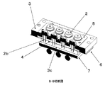
以下、本実施の形態にかかるレーザアレイ光源ユニット1を、図面を参照しながら説明する。図1は、本実施の形態にかかるレーザアレイ光源ユニット1の説明図である。図2は、本実施の形態にかかる半導体レーザ2の説明図であり、図2(a)は、本実施の形態にかかる半導体レーザ2の発光面側の斜視図であり、図2(b)は、本実施の形態にかかる半導体レーザ2の裏面側の斜視図である。図3は、本実施の形態にかかるレーザホルダ3の説明図である。図4は、本実施の形態にかかるインシュレータ4の説明図であり、図4(a)は、本実施の形態にかかるインシュレータ4の斜視図であり、図4(b)は、図4(a)にかかるインシュレータ4をA−Aの位置で切断した切断図である。図4(c)は、図4(b)におけるインシュレータ4の貫通孔4aの拡大断面図である。
(Embodiment 1)
Hereinafter, the laser array
図1に示されるように、レーザアレイ光源ユニット1は、複数の半導体レーザ2の本体部2aが、押さえ部材5によりレーザホルダ3に付勢された状態で保持されてなる。図1では図示しない裏面に向けて、半導体レーザ2の足部2bが、レーザホルダ3の貫通孔3aを貫通している。レーザホルダ3の貫通孔3aを貫通した足部2bのそれぞれのリード電極は、それぞれのリード電極を挿入することのできるインシュレータ4の貫通孔4aをさらに貫通し、配線基材6に設けられた第1の貫通孔6cを貫通する。これらの部材を貫通したそれぞれのリード電極は、半田により半田付けされ、固定される。以下、それぞれの部材およびこれらの配置について説明する。
As shown in FIG. 1, the laser array
<半導体レーザ>
半導体レーザ2について説明する。半導体レーザ2は、レーザアレイ光源ユニット1において光源として機能する。半導体レーザ2は、図2(a)および図2(b)に示されるように、本体部2aと、2本のリード電極からなる足部2bとからなる。本体部2aには、レーザ光を発するレーザ発光部2cが設けられている。本体部2aの形状としては、レーザ発光部2cを中心とした膨出部2dと、膨出部2dの周囲に設けられた縁部2eとからなる。縁部2eには、切欠き2fが設けられており、かかる切欠き2fは、後述するレーザホルダ3の貫通孔3aへ半導体レーザ2の足部2bを挿入する際の目安として機能する。縁部2eは、押さえ部材5と当接するため、押さえ部材5により半導体レーザ2はレーザホルダ3に付勢される。図2に示されるように、半導体レーザ2の裏面には、2本のリード電極からなる足部2bが設けられている。リード電極は、複数の半導体レーザ2を一列または縦横に並べた際に、1つの半導体レーザ2のアノードと、隣り合う半導体レーザ2のカソードとが横並びとなるよう配置される。かかる配置を取ることにより、半導体レーザ2のそれぞれのリード電極を後述する配線基材6と接続した際に、電気的直列に接続されることとなる。
<Semiconductor laser>
The
リード電極の線径としては、半導体レーザ2の種類により種々のものが存在するため一概に決定することはできないが、本実施の形態では、0.45±0.10mmのものを使用することができ、1つの半導体レーザ2におけるリード電極のアノードとカソードとは、2.54mm程度離間されている。
The wire diameter of the lead electrode cannot be determined unconditionally because there are various types depending on the type of the
<レーザホルダ>
レーザホルダ3について説明する。レーザホルダ3は、半導体レーザ2を保持するホルダとして機能する。レーザホルダ3は、図3に示されるように、半導体レーザ2の本体部2aの裏面が当接して半導体レーザ2を保持する受け面3bが設けられている。受け面3bの略中央部には、半導体レーザ2の足部2bを挿入することのできる貫通孔3aが設けられている。レーザホルダ3の受け面3bおよび貫通孔3aは、使用する半導体レーザ2の個数および配列に併せて設けられ、図3では、4個×6個の半導体レーザ2を使用する場合を想定して、計24個の受け面3bおよび貫通孔3aが設けられている。
<Laser holder>
The
受け面3bは、半導体レーザ2の本体部2aと当接することにより、半導体レーザ2から発せられる熱を伝播することができる。そのため、受け面3bは熱伝導性のよい材料で構成されており、本実施の形態では、アルミニウム製の受け面3bを有するレーザホルダ3から構成されている。
The receiving
貫通孔3aの形状としては特に限定されないが、隣り合う貫通孔3aに、それぞれ半導体レーザ2のリード電極を挿入した際に、挿入後のリード電極のアノードとカソードが一列に整列することが好ましい。そのため、たとえば図3に示されるような角が丸い長方形の断面形状を呈していることが好ましい。
The shape of the through
<インシュレータ>
インシュレータ4について説明する。一般に、半導体レーザ2の足部2bをレーザホルダ3の貫通孔3aに挿入した後に、貫通した足部2bのそれぞれのリード電極は、後述する配線基材6と接続するために長さが余分に設けられている。その場合、それぞれのリード電極は、物理的・電気的に接触してショートする可能性がある。そのため、それぞれのリード電極が挿入される貫通孔4aが形成された電極挿入部4fが複数設けられたインシュレータ4を使用し、それぞれのリード電極が物理的・電気的に接触しないよう貫通孔4aが設けられる。
<Insulator>
The
図4(b)に示されるように、インシュレータ4は、それぞれのリード電極が挿入される貫通孔4aが設けられており、1つの半導体レーザ2の2本のリード電極を通す貫通孔4aが形成された電極挿入部4fと、他の隣り合う半導体レーザ2の2本のリード電極を通す貫通孔4aが形成された電極挿入部4fとが、連結部4bにより連結されてなる。連結部4bは、複数の半導体レーザ2の配列方向と同方向に設けられてなる。このように、連結部4bを用いて一列に接続することにより、複数の半導体レーザ2のそれぞれに対応するインシュレータを複数個用意する場合と比較して、インシュレータの位置決めが容易となり、製造時の作業の効率化を図ることができる。連結部4bの形状として特に限定されないが、図4(b)に示されるように、リード電極出口4eが設けられた面と面一に形成されてなることが好ましい。かかる構成を有することにより、連結部4bが後述する配線基材6に沿って配置されることとなり、連結部4bがレーザアレイ光源ユニット1において放熱に利用される空間を狭めることがなく、半導体レーザ2より発生した熱を効率的に放熱する空間を充分に確保することができる。
As shown in FIG. 4B, the
インシュレータ4を構成する材料としては、絶縁性を有するものであれば特に限定することなく使用することができる。本実施の形態では、高耐熱性、耐薬品性、精密成形性に優れたポリフェニレンサルファイド樹脂(PPS)製のインシュレータ4が採用されている。
Any material can be used for the
図4(b)に示されるように、インシュレータ4の貫通孔4aは、リード電極を挿入するリード電極挿入口4cと、挿入方向に沿ってテーパ状に縮径されて形成された細径部4dと、該細径部4dから逆テーパ状に拡径されたリード電極出口4eを有する。このように、貫通孔4aは、リード電極の挿入方向に沿ってテーパ状に縮径された構造を有しているため、レーザアレイ光源ユニット1の組立時において、インシュレータ4の貫通孔4aへのリード電極の挿入が容易となり、挿入ミスや、挿入ミスに起因するリード電極の破損を防ぐことができる。また、細径部4dが設けられていることにより、リード電極を当接しながら保持することができ、レーザホルダ3に挿入された半導体レーザ2の位置を、より確実に定めることができるとともに、それぞれのリード電極を物理的・電気的により確実に分離することができる。さらに、細径部4dからリード電極出口4eにかけて逆テーパ状に拡径されているため、半田付けを行った場合に半田盛りが逆テーパ部分に入り込むことができ、半田不良を生じることがない。リード電極挿入口4cの径としては特に限定されないが、上記した半導体レーザ2のリード電極の線径が0.45±0.10mmであり、1つの半導体レーザ2におけるリード電極のアノードとカソードとが、それぞれ2.54mm程度離間されている場合には、たとえば1.4mm程度である。同様に、リード電極出口4eの径は、たとえば0.9mm程度であり、細径部4dの径は、たとえば0.70mm程度である。
As shown in FIG. 4B, the through
<配線基材>
配線基材6について説明する。配線基材6は、半導体レーザ2を電気的直列に配線する基材である。配線基材6を形成する材料としては特に限定されないが、フレキシブルプリント基板を採用することができる。フレキシブルプリント基板を構成する絶縁部6a(ベースフィルム)や導電部6bを構成する材料としては、公知のものを使用することができ、たとえば絶縁部6aとしてはポリイミドフィルム、導電部6bとしては銅を採用することができる。
<Wiring substrate>
The
図5は、本実施の形態にかかる配線基材6の説明図である。図5に示されるように、導電部6bと絶縁部6aとから構成される。導電部6bには、1つの半導体レーザ2のリード電極のアノードと、隣り合う半導体レーザ2のリード電極のカソードとが電気的に接続されるよう、アノードのリード電極とカソードのリード電極のそれぞれに対して、半導体レーザ2のリード電極を挿入する第1の貫通孔6cが設けられている。
FIG. 5 is an explanatory diagram of the
図5では、横並びに4個の半導体レーザ2を配置したものを1列とし、その列を6列設けた場合の配線基材6の導電部6bの構成を示しており、隣り合う4個の半導体レーザ2が1列をなし、さらに、隣り合う2列が電気的直列に接続されてなる。このように、配線基材6を配置することにより、上記したインシュレータ4の連結部4bと配線基材6の導電部6bとが重なるように配置されることとなる。その結果、レーザアレイ光源ユニット1の内部空間において、配線基材6は、インシュレータ4の下に敷設された構成となり、半導体レーザ2より発生した熱を効率的に放熱する空間を充分に確保することができる。
FIG. 5 shows the configuration of the
配線基材6の第1の貫通孔6cの孔径は、インシュレータ4の貫通孔4aを貫通した半導体レーザ2のそれぞれのリード電極が、容易に第1の貫通孔6c内に挿入されるよう、インシュレータ4の細径部4dよりも大きく形成されてなることが好ましく、かつ、第1の貫通孔6cとリード電極の線径との差(リード電極の直径と第1の貫通孔6cとの挿入余裕幅の2倍)と、リード電極の直径との和にほぼ等しいことが好ましい。第1の貫通孔6cの孔径が、この程度の大きさで構成されていることにより、インシュレータ4の貫通孔4aを貫通した半導体レーザ2のそれぞれのリード電極は、配線基材6の第1の貫通孔6cを容易に貫通することができ、かつ、半田付けをした際に半田不良を生じることもない。第1の貫通孔6cの孔径の具体例としては、上記した半導体レーザ2のリード電極の線径が0.45±0.10mmであり、第1の貫通孔6cにリード電極を挿入した場合の挿入余裕幅が0.25mm程度の場合には、たとえば0.95mm程度となる。
The diameter of the first through
配線基材6のうち、半導体レーザの各列に対してそれぞれ設けられた列配線部6eの幅は、上記した配線基材6の第1の貫通孔6cの孔径と、半田付けをした際の半田パターンの幅の2倍と、列配線部6eの余裕幅の2倍との和にほぼ等しいことが好ましく、かつ、インシュレータ4の幅とほぼ等しいことが好ましい。配線基材6の列配線部6eの幅が、この程度の幅で構成されていることにより、インシュレータ4が配置された箇所と重なる位置に配線基材6の列配線部6eが配置されることになり、配線基材6がレーザアレイ光源ユニット1の放熱に利用される空間を余分に占めることがなく、半導体レーザ2より発生した熱を効率的に放熱する空間を充分に確保することができる。配線基材6の列配線部6eの幅の具体例としては、上記した第1の貫通孔6cの孔径が0.95mm程度であり、列配線部6eの余裕幅が0.4mm程度であり、半田パターンの幅が0.3mm程度の場合には、たとえば2.4mm程度となる。列配線部6eの幅と、インシュレータ4の幅とはほぼ等しいため、インシュレータ4の幅もたとえば2.4mm程度となる。
Of the
<押さえ部材>
押さえ部材5について説明する。押さえ部材5は、半導体レーザ2の本体部2aと、レーザホルダ3の受け面3bとが接触するよう付勢する部材である。図1、図6A〜図6Cおよび図7Aに示されるように、押さえ部材5の貫通孔5aは、半導体レーザ2の膨出部2dよりも大きな径を有し、かつ、縁部2eよりも小さな径を有する。そのため、押さえ部材5の貫通孔5aに半導体レーザ2の膨出部2dを挿入して半導体レーザ2の本体部2aをレーザホルダ3に付勢すると、半導体レーザ2より発生した熱が放熱される。押さえ部材5は、レーザホルダ3のねじ穴にねじを締め付けることにより、レーザホルダ3に固着されている。
<Presser member>
The holding
押さえ部材5の材質としては特に限定されないが、保持と放熱性の観点から、図1にかかるレーザアレイ光源ユニット1では、バネ性のあるステンレス製の押さえ部材5が使用されている。このように、押さえ部材5を板ばねとして機能させて半導体レーザ2をレーザホルダ3に押さえつけたのち、半導体レーザ2のそれぞれのリード電極は、配線基材6と半田付けにより固着される。
The material of the
<冷却装置>
冷却装置7について説明する。冷却装置7は、本発明にかかるレーザアレイ光源ユニット1の使用時において、それぞれの半導体レーザ2から発生する熱をより効率よく放熱するために予備的に設けられる。
<Cooling device>
The
冷却装置7の種類としては特に限定されず、風冷式、気体冷却式、相変化冷却式、液冷却式の各種冷却方式を採用した冷却装置を使用することができる。図1に示されるように、本実施の形態では、銅製のヒートパイプからなる冷却装置7が採用されている。
The type of the
冷却装置7(放熱器、又は、ヒートシンク)の設置場所としては特に限定されず、たとえば半導体レーザ2のレーザ発光部2cから発せられるレーザの進路を阻害しない態様において、半導体レーザ2の斜め前方から風冷式の冷却装置を配置してもよく、図1に示されるようにレーザホルダ3の裏面(受け面3bが形成された面から見た反対面)に接触させてもよい。
The installation location of the cooling device 7 (heat radiator or heat sink) is not particularly limited. For example, in a mode that does not hinder the course of the laser emitted from the laser light emitting unit 2c of the
レーザホルダ3と冷却装置7との位置関係について説明する。レーザホルダ3と冷却装置7とは、レーザホルダ3の裏面と冷却装置7とが接触している。すなわち、レーザホルダ3の裏面は、半導体レーザ2より発生した熱を放熱するための放熱面として機能する。また、冷却装置7において、当該レーザホルダ3の放熱面と接触する面は、受熱面として機能する。このように、放熱面と受熱面を接触させる構成としては、以下の構成を挙げることができる。
The positional relationship between the
第1の態様としては、図6A〜図6Dに示される。図6A〜図6Dは、レーザホルダ3と冷却装置7との接触状態を説明する説明図であり、図6Aはレーザアレイ光源ユニット1の全体図を示しており、図6Bは、図6Aに示されたレーザアレイ光源ユニット1をA−Aの位置で切断した切断図を示しており、図6Cは、図6Aに示されたレーザアレイ光源ユニット1をB−Bの位置で切断した切断図を示しており、図6Dは、図6Cの切断図をほぼ側面方向から示している。図6B〜Dに示されるように、半導体レーザ2をインシュレータ4と配線基材6とを介してレーザホルダ3に取付けた状態において、レーザホルダ3の裏面には、配線基材6の第1の貫通孔6cより突出したリード電極よりも、突出長が長い冷却装置接触部3cを有している。冷却装置接触部3cは、レーザホルダ3の裏面から突出し、配線基材6の列配線部6e間を通過している。配線基材6の裏面からの突出長について、冷却装置接触部3cとリード電極を比較すると冷却装置接触部3cの方が長い。そして、当該冷却装置接触部3cの端部が放熱面として機能し、冷却装置7の受熱面と接触している。このように、第1の態様では、冷却装置7の受熱面を平面で構成することができるため、冷却効率を向上させることができる。また、冷却装置7の受熱面の構造が単純であるため、製造コストを低減することができる。
The first aspect is shown in FIGS. 6A to 6D. 6A to 6D are explanatory views for explaining the contact state between the
第2の態様としては、図7A〜図7Cに示される。図7A〜図7Cは、レーザホルダ3と冷却装置7との接触状態を説明する説明図であり、図7Aはレーザアレイ光源ユニットの全体図を示しており、図7Bは、図7Aに示されたレーザアレイ光源ユニットをA−Aの位置で切断した切断図を示しており、図7Cは、図7Aに示されたレーザアレイ光源ユニットをB−Bの位置で切断した切断図を示している。図7Bおよび図7Cに示されるように、半導体レーザ2をインシュレータ4と配線基材6とを介してレーザホルダ3に取付けた状態において、レーザホルダ3の裏面に突出したリード電極の余分は、冷却装置7に設けられた凹部7aに挿入されている。凹部7aは、リード電極が冷却装置7と非接触状態で挿入され得る深さを有するよう構成されている。そして、レーザホルダ3の裏面が放熱面となり、冷却装置7の受熱面と接触している。図6Cおよび図6Dに示される第1の態様と比較して明らかなように、このように冷却装置7に凹部7aを設けることによって、冷却装置7を小型にすることができる。その結果、レーザアレイ光源ユニットそのものも小型化することができる。
The second aspect is shown in FIGS. 7A to 7C. 7A to 7C are explanatory views for explaining the contact state between the
(実施の形態2)
本実施の形態にかかるレーザアレイ光源ユニットの構成について、図8を参照しながら説明する。図8は、本実施の形態にかかる配線基材6とレーザホルダ3との位置を説明する説明図である。図8に示されるように、配線基材6は、リード電極を挿入する第1の貫通孔6cとは異なる第2の貫通孔6dを有し、当該第2の貫通孔6dは、レーザホルダ3に設けられた基準ピン3eを通す孔である。基準ピン3eが第2の貫通孔6dを貫通した状態において、配線基材6に設けられた第1の貫通孔6cは、インシュレータ4の貫通孔4aと対応する位置に配置されるよう構成されている。なお、かかる構成以外については実施の形態1において説明した構成を採用することができるため、同一の参照符号を付して説明を省略する。
(Embodiment 2)
The configuration of the laser array light source unit according to the present embodiment will be described with reference to FIG. FIG. 8 is an explanatory diagram for explaining the positions of the
このように、配線基材6に第2の貫通孔6dを設け、レーザホルダ3の基準ピン3eを貫通させることで、自動的に第1の貫通孔6cとインシュレータ4の貫通孔4aが対応する位置に位置決めされる。その結果、インシュレータ4の貫通孔4aに半導体レーザ2のリード電極が挿入される際の挿入ミスや、挿入ミスに起因するリード電極の破損をより確実に防ぐことができる。
As described above, by providing the
(実施の形態3)
本実施の形態にかかるレーザアレイ光源ユニットの構成について、図9Aおよび図9Bを参照しながら説明する。図9Aは、本実施の形態にかかる配線基材6とレーザホルダ3と冶具8との位置を説明する説明図であり、図9Bは、配線基材6とレーザホルダ3との位置を説明する説明図であり、冶具8を取り外した状態における配線基材6とレーザホルダ3との位置関係を説明するために示している。ここでいう冶具8とは、実際の製造工程において、レーザアレイ光源ユニットを組み立てる際に使用される部材である。
(Embodiment 3)
The configuration of the laser array light source unit according to the present embodiment will be described with reference to FIGS. 9A and 9B. FIG. 9A is an explanatory diagram for explaining the positions of the
この場合、図9Aに示されるように、配線基材6は、リード電極を挿入する第1の貫通孔6cとは異なる第2の貫通孔6dを有し、当該第2の貫通孔6dには、レーザホルダ3に設けられた基準孔3dとともに、冶具8に設けられた基準ピン8aが通される。基準ピン8aがレーザホルダ3の基準孔3dと、配線基材6の第2の貫通孔6dを貫通した状態において、配線基材6に設けられた第1の貫通孔6cは、インシュレータ4の貫通孔4aと対応する位置に配置されるよう構成されている。なお、かかる構成以外については実施の形態1において説明した構成を採用することができるため、同一の参照符号を付して説明を省略する。
In this case, as shown in FIG. 9A, the
このように、配線基材6に第2の貫通孔6dを設け、レーザホルダ3の基準孔3dとともに冶具8の基準ピン8aを貫通させることで、自動的に第1の貫通孔6cとインシュレータ4の貫通孔4aとが対応する位置に位置決めされる。その結果、インシュレータ4の貫通孔4aに半導体レーザ2のリード電極が挿入される際の挿入ミスや、挿入ミスに起因するリード電極の破損をより確実に防ぐことができる。
As described above, the second through
(実施の形態4)
本実施の形態にかかるプロジェクタについて、図10を参照しながら説明する。図10は、本発明にかかるレーザアレイ光源ユニット1を使用したプロジェクタ9の構成を説明する模式図である。図10に示されるように、それぞれの半導体レーザ2から発せられた光は、それぞれの半導体レーザ2の前に設けられたコリメートレンズ10によりコリメートされた後、集光レンズ11を通過する。その後、ダイクロイックミラー12と第1コンデンサレンズ群13aを透過し、緑の蛍光体が塗布された蛍光体ホイール14に励起され、半導体レーザ光と反対方向に緑色が発光する。発光した光は、第1コンデンサレンズ群13aを戻り、緑反射ダイクロイックミラー12Gで反射され、青反射ダイクロイックミラー12B、赤反射ダイクロイックミラー12R、第2コンデンサレンズ13bを透過し、ロッドインテグレータ16に入射される。青色LED15Bと赤色LED15Rは、第1コンデンサレンズ群13aを透過し、青反射ダイクロイックミラー12B、および赤反射ダイクロイックミラー12Rで各色のLED光を反射し、第2コンデンサレンズ13bを透過し、ロッドインテグレータ16に入射される。ロッドインテグレータ16を経て均一化された光は、リレーレンズ17および反射レンズ18を経てDMD19(デジタルマイクロミラーデバイス)を通過する。DMD19を通過した光は投射レンズ20を通過し、対象物に投射される。
(Embodiment 4)
The projector according to the present embodiment will be described with reference to FIG. FIG. 10 is a schematic diagram for explaining the configuration of the
なお、本発明のレーザアレイ光源ユニットは、プロジェクタ以外にも、複写機、ファクシミリ、プリンタ、デジタルラボなどの各種画像形成装置の操作光学系に使用することができる。 In addition to the projector, the laser array light source unit of the present invention can be used for an operation optical system of various image forming apparatuses such as a copying machine, a facsimile, a printer, and a digital laboratory.
本発明のレーザアレイ光源ユニットは、複数の半導体レーザから発せられる熱が効率的に放熱されるよう配置されたレーザアレイ光源ユニットであり、半導体レーザより発生した熱を効率的に放熱することができ、かつ、組立が容易であり、さらに、複数の半導体レーザを密に配置した場合であっても物理的・電気的に分離した構成を有するレーザアレイ光源ユニットを提供することができるため、たとえばプロジェクタ等に使用する画像形成装置の操作光学系等に用いることができる。 The laser array light source unit of the present invention is a laser array light source unit arranged so that heat generated from a plurality of semiconductor lasers can be efficiently dissipated, and can efficiently dissipate heat generated from the semiconductor lasers. In addition, since a laser array light source unit having a configuration that is physically and electrically separated even when a plurality of semiconductor lasers are densely arranged can be provided. For example, it can be used in an operation optical system of an image forming apparatus used for the above.
1 レーザアレイ光源ユニット
2 半導体レーザ
2a 本体部
2b 足部
2c レーザ発光部
2d 膨出部
2e 縁部
2f 切欠き
3 レーザホルダ
3a、4a、5a 貫通孔
3b 受け面
3c 冷却装置接触部
3d 基準孔
3e、8a 基準ピン
4 インシュレータ
4b 連結部
4c リード電極挿入口
4d 細径部
4e リード電極出口
4f 電極挿入部
5 押さえ部材
6 配線基材
6a 絶縁部
6b 導電部
6c 第1の貫通孔
6d 第2の貫通孔
6e 列配線部
7 冷却装置
7a 凹部
8 冶具
9 プロジェクタ
10 コリメートレンズ
11 集光レンズ
12G 緑反射ダイクロイックミラー
12B 青反射ダイクロイックミラー
12R 赤反射ダイクロイックミラー
13a 第1コンデンサレンズ群
13b 第2コンデンサレンズ
14 蛍光体ホイール
15B 青色LED
15R 赤色LED
16 ロッドインテグレータ
17 リレーレンズ
18 反射レンズ
19 DMD
20 投射レンズ
DESCRIPTION OF
15R Red LED
16
20 Projection lens
Claims (9)
該半導体レーザの本体部を保持する受け面を有し、前記半導体レーザの足部を挿入する貫通孔を備えたレーザホルダと、
前記半導体レーザのそれぞれのリード電極を挿入する貫通孔が形成された電極挿入部を複数有するインシュレータと、
前記複数の半導体レーザの少なくとも2個以上を電気的直列に接続するための配線基材とを含み、
前記インシュレータは、前記複数の半導体レーザの配列方向と同方向に、前記電極挿入部の間を接続するための連結部を有し、
前記配線基材には、前記半導体レーザのそれぞれのリード電極を挿入する第1の貫通孔が設けられており、前記インシュレータに沿って配列された半導体レーザの各列に対してそれぞれ設けられた列配線部の幅は、前記インシュレータの幅とほぼ等しいことを特徴とするレーザアレイ光源ユニット。 A plurality of semiconductor lasers comprising a main body part and a foot part comprising two lead electrodes;
A laser holder having a receiving surface for holding the main body of the semiconductor laser, and a through-hole for inserting a foot of the semiconductor laser;
An insulator having a plurality of electrode insertion portions each having a through hole into which each lead electrode of the semiconductor laser is inserted;
A wiring substrate for electrically connecting at least two of the plurality of semiconductor lasers in electrical series;
The insulator has a connecting portion for connecting the electrode insertion portions in the same direction as the arrangement direction of the plurality of semiconductor lasers,
The wiring substrate is provided with first through holes into which the respective lead electrodes of the semiconductor lasers are inserted, and columns provided for the respective columns of the semiconductor lasers arranged along the insulator. The laser array light source unit according to claim 1 , wherein a width of the wiring portion is substantially equal to a width of the insulator .
該放熱面と接触する受熱面を有する冷却装置がさらに含まれてなる請求項1記載のレーザアレイ光源ユニット。 In the laser holder, a heat dissipation surface is formed on the opposite surface seen from the surface on which the receiving surface of the laser holder is formed,
The laser array light source unit according to claim 1, further comprising a cooling device having a heat receiving surface in contact with the heat radiating surface.
前記リード電極を挿入するリード電極挿入口と、
挿入方向に沿ってテーパ状に縮径されて形成された細径部と、
該細径部から逆テーパ状に拡径されたリード電極出口とを有することを特徴とする請求項1記載のレーザアレイ光源ユニット。 The insulator through-hole into which the lead electrode is inserted is
A lead electrode insertion slot for inserting the lead electrode;
A narrow-diameter portion formed by being tapered in a taper shape along the insertion direction;
The laser array light source unit according to claim 1, further comprising: a lead electrode outlet that is expanded in a reverse taper shape from the narrow diameter portion.
た面と面一に形成されてなることを特徴とする請求項1に記載のレーザアレイ光源ユニット。 2. The laser array light source unit according to claim 1 , wherein the connecting portion of the insulator is formed flush with a surface of the electrode insertion portion where the lead electrode outlet is formed.
該第2の貫通孔は、
前記レーザホルダに基準ピンが設けられる場合において、該基準ピンを通す孔であり、
前記第2の貫通孔に前記基準ピンが挿入された状態において、前記配線基材に設けられた前記第1の貫通孔が、前記インシュレータの貫通孔と対応する位置に配置される請求項5記載のレーザアレイ光源ユニット。 The wiring substrate has a second through hole different from the first through hole into which the lead electrode is inserted,
The second through hole is
When a reference pin is provided in the laser holder, it is a hole through which the reference pin passes.
In a state in which the reference pin into the second through-holes are inserted, the provided on the wiring substrate first through hole, according to claim 5, wherein disposed in a position corresponding to the through hole of the insulator Laser array light source unit.
該第2の貫通孔は、
前記レーザホルダに基準孔が設けられ、かつ、該レーザホルダを保持するために用いられる冶具に前記基準孔に通す基準ピンが設けられる場合において、該基準ピンを通す孔であり、
前記第2の貫通孔および前記基準孔に前記基準ピンが挿入された状態において、前記配線基材に設けられた前記第1の貫通孔が、前記インシュレータの貫通孔と対応する位置に配置される請求項5記載のレーザアレイ光源ユニット。 The wiring substrate has a second through hole different from the first through hole into which the lead electrode is inserted,
The second through hole is
In the case where a reference hole is provided in the laser holder, and a reference pin that passes through the reference hole is provided in a jig used to hold the laser holder, the hole through which the reference pin passes,
In a state where the reference pin is inserted into the second through hole and the reference hole, the first through hole provided in the wiring substrate is disposed at a position corresponding to the through hole of the insulator. The laser array light source unit according to claim 5 .
前記レーザホルダは、前記レーザホルダの受け面が形成された面から見た反対面に、前記配線基材の第1の貫通孔より突出した前記半導体レーザのそれぞれのリード電極よりも突出長が大きい冷却装置接触部を有し、
該冷却装置接触部の端部に形成された放熱面と、前記冷却装置の受熱面とが接触することを特徴とする請求項2記載のレーザアレイ光源ユニット。 In a state where the plurality of semiconductor lasers are attached to the laser holder via the insulator and the wiring base material,
The projecting length of the laser holder is larger than each lead electrode of the semiconductor laser projecting from the first through hole of the wiring substrate on the opposite surface as viewed from the surface on which the receiving surface of the laser holder is formed. A cooling device contact portion,
3. The laser array light source unit according to claim 2, wherein a heat radiation surface formed at an end of the cooling device contact portion and a heat receiving surface of the cooling device are in contact with each other.
前記冷却装置は、前記配線基材の第1の貫通孔より突出した前記半導体レーザのそれぞれのリード電極が前記冷却装置と非接触状態で挿入され得る深さの凹部を有し、
前記レーザホルダの受け面が形成された面から見た反対面に形成された放熱面と、前記冷却装置の受熱面とが接触することを特徴とする請求項2記載のレーザアレイ光源ユニット。 In a state where the plurality of semiconductor lasers are attached to the laser holder via the insulator and the wiring base material,
The cooling device has a recess having a depth at which each lead electrode of the semiconductor laser protruding from the first through hole of the wiring substrate can be inserted in a non-contact state with the cooling device;
3. The laser array light source unit according to claim 2, wherein a heat radiating surface formed on an opposite surface as viewed from a surface on which the receiving surface of the laser holder is formed contacts a heat receiving surface of the cooling device.
Priority Applications (2)
| Application Number | Priority Date | Filing Date | Title |
|---|---|---|---|
| JP2012095882A JP5934914B2 (en) | 2011-05-13 | 2012-04-19 | Laser array light source unit |
| US13/469,102 US8718109B2 (en) | 2011-05-13 | 2012-05-11 | Laser array light source unit |
Applications Claiming Priority (3)
| Application Number | Priority Date | Filing Date | Title |
|---|---|---|---|
| JP2011108705 | 2011-05-13 | ||
| JP2011108705 | 2011-05-13 | ||
| JP2012095882A JP5934914B2 (en) | 2011-05-13 | 2012-04-19 | Laser array light source unit |
Publications (3)
| Publication Number | Publication Date |
|---|---|
| JP2012256860A JP2012256860A (en) | 2012-12-27 |
| JP2012256860A5 JP2012256860A5 (en) | 2014-11-27 |
| JP5934914B2 true JP5934914B2 (en) | 2016-06-15 |
Family
ID=47141855
Family Applications (1)
| Application Number | Title | Priority Date | Filing Date |
|---|---|---|---|
| JP2012095882A Active JP5934914B2 (en) | 2011-05-13 | 2012-04-19 | Laser array light source unit |
Country Status (2)
| Country | Link |
|---|---|
| US (1) | US8718109B2 (en) |
| JP (1) | JP5934914B2 (en) |
Families Citing this family (29)
| Publication number | Priority date | Publication date | Assignee | Title |
|---|---|---|---|---|
| JP6311424B2 (en) * | 2013-04-22 | 2018-04-18 | 日亜化学工業株式会社 | Light source device |
| JP6423997B2 (en) * | 2013-07-09 | 2018-11-14 | オリンパス株式会社 | Heat treatment apparatus for light source and light source apparatus |
| JP6187023B2 (en) * | 2013-08-20 | 2017-08-30 | セイコーエプソン株式会社 | Light source device and projector |
| DE102013217796A1 (en) * | 2013-09-05 | 2015-03-05 | Osram Opto Semiconductors Gmbh | Optoelectronic component, optoelectronic device and method for producing an optoelectronic device |
| JPWO2015145608A1 (en) * | 2014-03-26 | 2017-04-13 | 株式会社島津製作所 | Laser equipment |
| JP6460370B2 (en) * | 2014-05-22 | 2019-01-30 | カシオ計算機株式会社 | Light source device and image projection device |
| JP6492462B2 (en) * | 2014-08-29 | 2019-04-03 | 日亜化学工業株式会社 | Light source device |
| JP6507942B2 (en) * | 2014-08-29 | 2019-05-08 | 日亜化学工業株式会社 | Holding member for semiconductor light emitting device, light source device and manufacturing method thereof |
| US11848534B2 (en) | 2014-11-24 | 2023-12-19 | Evolve Additive Solutions, Inc. | Additive manufacturing system with laser assembly |
| JP6215857B2 (en) * | 2015-02-26 | 2017-10-18 | ファナック株式会社 | Air-cooled laser apparatus provided with an L-shaped heat conducting member having a radiation fin |
| JP6547562B2 (en) | 2015-09-30 | 2019-07-24 | 日亜化学工業株式会社 | Light source device |
| JP6720502B2 (en) * | 2015-10-30 | 2020-07-08 | 株式会社島津製作所 | Laser device manufacturing method |
| CN105428993A (en) * | 2015-12-30 | 2016-03-23 | 重庆贝华科技有限公司 | Coaxial laser bonding wire fixture device |
| CN109565147A (en) | 2016-07-28 | 2019-04-02 | Nec显示器解决方案株式会社 | The method of light supply apparatus, projection display equipment and cooling semiconductor light-emitting elements |
| CN209183945U (en) * | 2016-08-30 | 2019-07-30 | Nec显示器解决方案株式会社 | Light supply apparatus, light-source system and projection display device |
| JP6512455B2 (en) * | 2016-12-20 | 2019-05-15 | カシオ計算機株式会社 | Electronic device and projection device |
| CN106532428B (en) * | 2016-12-29 | 2024-02-09 | 西安炬光科技股份有限公司 | Refrigerating method and system for cooling medium and semiconductor laser |
| JP6971441B2 (en) * | 2017-09-28 | 2021-11-24 | 日亜化学工業株式会社 | Light source module and its manufacturing method |
| US10422514B2 (en) * | 2017-12-19 | 2019-09-24 | Sharp Kabushiki Kaisha | Light source module |
| JP7014645B2 (en) * | 2018-03-06 | 2022-02-01 | シャープ株式会社 | Semiconductor light emitting device |
| CN110277721A (en) * | 2018-03-16 | 2019-09-24 | 青岛海信激光显示股份有限公司 | A kind of laser die group, laser light source and laser projection device |
| CN208506478U (en) | 2018-07-23 | 2019-02-15 | 中强光电股份有限公司 | Liquid cooling radiation module and projection arrangement |
| CN208752384U (en) | 2018-09-25 | 2019-04-16 | 中强光电股份有限公司 | Projector and its laser module |
| CN109188823B (en) * | 2018-10-18 | 2021-07-13 | 华北水利水电大学 | Laser array light source for optical scanning |
| US11592145B2 (en) | 2019-01-10 | 2023-02-28 | Hisense Laser Display Co., Ltd. | Laser light source and laser projection device |
| US11570411B2 (en) * | 2019-01-10 | 2023-01-31 | Hisense Laser Display Co., Ltd. | Laser light source and laser projection device |
| JP7423924B2 (en) | 2019-07-22 | 2024-01-30 | 岩崎電気株式会社 | Light source unit and lighting device |
| US11821615B2 (en) | 2020-08-11 | 2023-11-21 | Signify Holding B.V. | System comprising luminescent material and two-phase cooling device |
| CN113009416B (en) * | 2021-04-08 | 2024-03-12 | 国网江苏省电力有限公司检修分公司 | Insulator detection positioning method based on laser sensor array |
Family Cites Families (7)
| Publication number | Priority date | Publication date | Assignee | Title |
|---|---|---|---|---|
| JP3642551B2 (en) | 1998-03-13 | 2005-04-27 | 日本オプネクスト株式会社 | Laser diode module, method for manufacturing the same, and laser diode |
| JP2001326411A (en) * | 2000-05-12 | 2001-11-22 | Hitachi Koki Co Ltd | Semiconductor laser device |
| JP2004325929A (en) * | 2003-04-25 | 2004-11-18 | Kyocera Mita Corp | Optical scanner |
| JP2005093599A (en) | 2003-09-16 | 2005-04-07 | Ricoh Opt Ind Co Ltd | Light source unit |
| JP4862597B2 (en) * | 2006-10-10 | 2012-01-25 | 富士ゼロックス株式会社 | Connection member, electric substrate, optical scanning device, and image forming apparatus |
| JP4871852B2 (en) * | 2007-12-05 | 2012-02-08 | シャープ株式会社 | Burn-in equipment |
| JP5473535B2 (en) * | 2009-10-28 | 2014-04-16 | 三菱電機株式会社 | Light source device |
-
2012
- 2012-04-19 JP JP2012095882A patent/JP5934914B2/en active Active
- 2012-05-11 US US13/469,102 patent/US8718109B2/en active Active
Also Published As
| Publication number | Publication date |
|---|---|
| US20120287954A1 (en) | 2012-11-15 |
| JP2012256860A (en) | 2012-12-27 |
| US8718109B2 (en) | 2014-05-06 |
Similar Documents
| Publication | Publication Date | Title |
|---|---|---|
| JP5934914B2 (en) | Laser array light source unit | |
| JP4467493B2 (en) | Backlight device and display device including the same | |
| US9341930B2 (en) | Light source device and projector | |
| US10054849B2 (en) | Light source device and projector | |
| US9323139B2 (en) | Light source device and projector | |
| US20150355533A1 (en) | Semiconductor element cooling structure and electronic apparatus provided with same | |
| JP2007265961A (en) | Luminaire | |
| JP2009032650A (en) | Lighting system, and luminaire | |
| JP6880855B2 (en) | Light source device and projector | |
| JP2007103748A (en) | Heat exchanger, liquid-cooling system, light source equipment, projector, electronic device unit, and electronic equipment | |
| JP6500223B2 (en) | Light source device and projection type image display device | |
| JP6187023B2 (en) | Light source device and projector | |
| JP4978053B2 (en) | Light emitting device and lighting device | |
| JP6205579B2 (en) | Light source device and projection display device | |
| JP2007103702A (en) | Heat exchanger, manufacturing method thereof, liquid-cooling system, light source equipment, projector, electronic device unit, and electronic equipment | |
| JP2005100810A (en) | Light source and projector | |
| JP2009170642A (en) | Electric device | |
| JP6137265B2 (en) | Light source device and projector | |
| JP7279571B2 (en) | Light source device and projector | |
| JP2018157057A (en) | Printed circuit board and electronic apparatus | |
| JP5436169B2 (en) | Light source device | |
| JP6811912B1 (en) | Laser light source device and manufacturing method of laser light source device | |
| JP6259998B2 (en) | Light source device and projection-type image display device using the same | |
| US20230209023A1 (en) | Light source assembly, optical engine, and projector | |
| JP2009252767A (en) | Light-emitting device |
Legal Events
| Date | Code | Title | Description |
|---|---|---|---|
| A711 | Notification of change in applicant |
Free format text: JAPANESE INTERMEDIATE CODE: A711 Effective date: 20141003 |
|
| RD02 | Notification of acceptance of power of attorney |
Free format text: JAPANESE INTERMEDIATE CODE: A7422 Effective date: 20141008 |
|
| A521 | Request for written amendment filed |
Free format text: JAPANESE INTERMEDIATE CODE: A523 Effective date: 20141010 |
|
| A621 | Written request for application examination |
Free format text: JAPANESE INTERMEDIATE CODE: A621 Effective date: 20141010 |
|
| A977 | Report on retrieval |
Free format text: JAPANESE INTERMEDIATE CODE: A971007 Effective date: 20150717 |
|
| A131 | Notification of reasons for refusal |
Free format text: JAPANESE INTERMEDIATE CODE: A131 Effective date: 20150804 |
|
| A521 | Request for written amendment filed |
Free format text: JAPANESE INTERMEDIATE CODE: A523 Effective date: 20150929 |
|
| TRDD | Decision of grant or rejection written | ||
| A01 | Written decision to grant a patent or to grant a registration (utility model) |
Free format text: JAPANESE INTERMEDIATE CODE: A01 Effective date: 20160301 |
|
| A61 | First payment of annual fees (during grant procedure) |
Free format text: JAPANESE INTERMEDIATE CODE: A61 Effective date: 20160314 |
|
| R151 | Written notification of patent or utility model registration |
Ref document number: 5934914 Country of ref document: JP Free format text: JAPANESE INTERMEDIATE CODE: R151 |