JP5934058B2 - In situ flexible circuit embossing to form electrical interconnects - Google Patents
In situ flexible circuit embossing to form electrical interconnects Download PDFInfo
- Publication number
- JP5934058B2 JP5934058B2 JP2012184354A JP2012184354A JP5934058B2 JP 5934058 B2 JP5934058 B2 JP 5934058B2 JP 2012184354 A JP2012184354 A JP 2012184354A JP 2012184354 A JP2012184354 A JP 2012184354A JP 5934058 B2 JP5934058 B2 JP 5934058B2
- Authority
- JP
- Japan
- Prior art keywords
- conductive pads
- embossed
- press
- flex circuit
- piezoelectric elements
- Prior art date
- Legal status (The legal status is an assumption and is not a legal conclusion. Google has not performed a legal analysis and makes no representation as to the accuracy of the status listed.)
- Expired - Fee Related
Links
- 238000004049 embossing Methods 0.000 title claims description 7
- 238000011065 in-situ storage Methods 0.000 title description 3
- 239000004020 conductor Substances 0.000 claims description 25
- 238000000034 method Methods 0.000 claims description 24
- 238000003825 pressing Methods 0.000 claims description 8
- 239000012811 non-conductive material Substances 0.000 claims description 6
- 239000002699 waste material Substances 0.000 claims 2
- 239000000976 ink Substances 0.000 description 46
- 239000010410 layer Substances 0.000 description 26
- 239000000463 material Substances 0.000 description 19
- 230000015572 biosynthetic process Effects 0.000 description 18
- 239000000853 adhesive Substances 0.000 description 16
- 230000001070 adhesive effect Effects 0.000 description 16
- 238000004519 manufacturing process Methods 0.000 description 9
- 238000013461 design Methods 0.000 description 8
- 238000012546 transfer Methods 0.000 description 7
- 238000005516 engineering process Methods 0.000 description 6
- 239000002184 metal Substances 0.000 description 6
- 229910052751 metal Inorganic materials 0.000 description 6
- 230000008569 process Effects 0.000 description 6
- 230000008878 coupling Effects 0.000 description 5
- 238000010168 coupling process Methods 0.000 description 5
- 238000005859 coupling reaction Methods 0.000 description 5
- 229910052451 lead zirconate titanate Inorganic materials 0.000 description 5
- PXHVJJICTQNCMI-UHFFFAOYSA-N Nickel Chemical compound [Ni] PXHVJJICTQNCMI-UHFFFAOYSA-N 0.000 description 4
- 238000007639 printing Methods 0.000 description 4
- 238000012545 processing Methods 0.000 description 4
- 239000003822 epoxy resin Substances 0.000 description 3
- 229920000647 polyepoxide Polymers 0.000 description 3
- 229910000679 solder Inorganic materials 0.000 description 3
- 239000004593 Epoxy Substances 0.000 description 2
- 239000012790 adhesive layer Substances 0.000 description 2
- 238000004891 communication Methods 0.000 description 2
- 230000007246 mechanism Effects 0.000 description 2
- 229910052759 nickel Inorganic materials 0.000 description 2
- 239000004033 plastic Substances 0.000 description 2
- 229920001169 thermoplastic Polymers 0.000 description 2
- 239000004416 thermosoftening plastic Substances 0.000 description 2
- 239000004677 Nylon Substances 0.000 description 1
- 229910045601 alloy Inorganic materials 0.000 description 1
- 239000000956 alloy Substances 0.000 description 1
- 238000003491 array Methods 0.000 description 1
- 239000003990 capacitor Substances 0.000 description 1
- 238000005229 chemical vapour deposition Methods 0.000 description 1
- 230000007423 decrease Effects 0.000 description 1
- 238000000280 densification Methods 0.000 description 1
- 238000000151 deposition Methods 0.000 description 1
- 230000008021 deposition Effects 0.000 description 1
- 238000010586 diagram Methods 0.000 description 1
- 238000001312 dry etching Methods 0.000 description 1
- 230000000694 effects Effects 0.000 description 1
- 238000007772 electroless plating Methods 0.000 description 1
- 229920006332 epoxy adhesive Polymers 0.000 description 1
- 230000009969 flowable effect Effects 0.000 description 1
- 239000012530 fluid Substances 0.000 description 1
- 238000007373 indentation Methods 0.000 description 1
- 238000000608 laser ablation Methods 0.000 description 1
- HFGPZNIAWCZYJU-UHFFFAOYSA-N lead zirconate titanate Chemical compound [O-2].[O-2].[O-2].[O-2].[O-2].[Ti+4].[Zr+4].[Pb+2] HFGPZNIAWCZYJU-UHFFFAOYSA-N 0.000 description 1
- 239000002991 molded plastic Substances 0.000 description 1
- 229920001778 nylon Polymers 0.000 description 1
- 239000006072 paste Substances 0.000 description 1
- 239000002985 plastic film Substances 0.000 description 1
- 229920001296 polysiloxane Polymers 0.000 description 1
- 230000037452 priming Effects 0.000 description 1
- 229920005989 resin Polymers 0.000 description 1
- 239000011347 resin Substances 0.000 description 1
- 230000004044 response Effects 0.000 description 1
- 230000002441 reversible effect Effects 0.000 description 1
- 238000007650 screen-printing Methods 0.000 description 1
- 238000000926 separation method Methods 0.000 description 1
- 238000005507 spraying Methods 0.000 description 1
- 238000003892 spreading Methods 0.000 description 1
- 230000007480 spreading Effects 0.000 description 1
- 238000004544 sputter deposition Methods 0.000 description 1
- 239000010935 stainless steel Substances 0.000 description 1
- 229910001220 stainless steel Inorganic materials 0.000 description 1
- 230000003746 surface roughness Effects 0.000 description 1
Images


Classifications
-
- B—PERFORMING OPERATIONS; TRANSPORTING
- B41—PRINTING; LINING MACHINES; TYPEWRITERS; STAMPS
- B41J—TYPEWRITERS; SELECTIVE PRINTING MECHANISMS, i.e. MECHANISMS PRINTING OTHERWISE THAN FROM A FORME; CORRECTION OF TYPOGRAPHICAL ERRORS
- B41J2/00—Typewriters or selective printing mechanisms characterised by the printing or marking process for which they are designed
- B41J2/005—Typewriters or selective printing mechanisms characterised by the printing or marking process for which they are designed characterised by bringing liquid or particles selectively into contact with a printing material
- B41J2/01—Ink jet
- B41J2/135—Nozzles
- B41J2/14—Structure thereof only for on-demand ink jet heads
- B41J2/14201—Structure of print heads with piezoelectric elements
- B41J2/14233—Structure of print heads with piezoelectric elements of film type, deformed by bending and disposed on a diaphragm
-
- B—PERFORMING OPERATIONS; TRANSPORTING
- B41—PRINTING; LINING MACHINES; TYPEWRITERS; STAMPS
- B41J—TYPEWRITERS; SELECTIVE PRINTING MECHANISMS, i.e. MECHANISMS PRINTING OTHERWISE THAN FROM A FORME; CORRECTION OF TYPOGRAPHICAL ERRORS
- B41J2/00—Typewriters or selective printing mechanisms characterised by the printing or marking process for which they are designed
- B41J2/005—Typewriters or selective printing mechanisms characterised by the printing or marking process for which they are designed characterised by bringing liquid or particles selectively into contact with a printing material
- B41J2/01—Ink jet
- B41J2/135—Nozzles
- B41J2/16—Production of nozzles
- B41J2/1607—Production of print heads with piezoelectric elements
- B41J2/161—Production of print heads with piezoelectric elements of film type, deformed by bending and disposed on a diaphragm
-
- B—PERFORMING OPERATIONS; TRANSPORTING
- B41—PRINTING; LINING MACHINES; TYPEWRITERS; STAMPS
- B41J—TYPEWRITERS; SELECTIVE PRINTING MECHANISMS, i.e. MECHANISMS PRINTING OTHERWISE THAN FROM A FORME; CORRECTION OF TYPOGRAPHICAL ERRORS
- B41J2/00—Typewriters or selective printing mechanisms characterised by the printing or marking process for which they are designed
- B41J2/005—Typewriters or selective printing mechanisms characterised by the printing or marking process for which they are designed characterised by bringing liquid or particles selectively into contact with a printing material
- B41J2/01—Ink jet
- B41J2/135—Nozzles
- B41J2/16—Production of nozzles
- B41J2/1621—Manufacturing processes
- B41J2/1623—Manufacturing processes bonding and adhesion
-
- Y—GENERAL TAGGING OF NEW TECHNOLOGICAL DEVELOPMENTS; GENERAL TAGGING OF CROSS-SECTIONAL TECHNOLOGIES SPANNING OVER SEVERAL SECTIONS OF THE IPC; TECHNICAL SUBJECTS COVERED BY FORMER USPC CROSS-REFERENCE ART COLLECTIONS [XRACs] AND DIGESTS
- Y10—TECHNICAL SUBJECTS COVERED BY FORMER USPC
- Y10T—TECHNICAL SUBJECTS COVERED BY FORMER US CLASSIFICATION
- Y10T29/00—Metal working
- Y10T29/42—Piezoelectric device making
-
- Y—GENERAL TAGGING OF NEW TECHNOLOGICAL DEVELOPMENTS; GENERAL TAGGING OF CROSS-SECTIONAL TECHNOLOGIES SPANNING OVER SEVERAL SECTIONS OF THE IPC; TECHNICAL SUBJECTS COVERED BY FORMER USPC CROSS-REFERENCE ART COLLECTIONS [XRACs] AND DIGESTS
- Y10—TECHNICAL SUBJECTS COVERED BY FORMER USPC
- Y10T—TECHNICAL SUBJECTS COVERED BY FORMER US CLASSIFICATION
- Y10T29/00—Metal working
- Y10T29/49—Method of mechanical manufacture
- Y10T29/49002—Electrical device making
- Y10T29/49117—Conductor or circuit manufacturing
- Y10T29/49124—On flat or curved insulated base, e.g., printed circuit, etc.
- Y10T29/49126—Assembling bases
-
- Y—GENERAL TAGGING OF NEW TECHNOLOGICAL DEVELOPMENTS; GENERAL TAGGING OF CROSS-SECTIONAL TECHNOLOGIES SPANNING OVER SEVERAL SECTIONS OF THE IPC; TECHNICAL SUBJECTS COVERED BY FORMER USPC CROSS-REFERENCE ART COLLECTIONS [XRACs] AND DIGESTS
- Y10—TECHNICAL SUBJECTS COVERED BY FORMER USPC
- Y10T—TECHNICAL SUBJECTS COVERED BY FORMER US CLASSIFICATION
- Y10T29/00—Metal working
- Y10T29/49—Method of mechanical manufacture
- Y10T29/49002—Electrical device making
- Y10T29/49117—Conductor or circuit manufacturing
- Y10T29/49124—On flat or curved insulated base, e.g., printed circuit, etc.
- Y10T29/49147—Assembling terminal to base
- Y10T29/49151—Assembling terminal to base by deforming or shaping
-
- Y—GENERAL TAGGING OF NEW TECHNOLOGICAL DEVELOPMENTS; GENERAL TAGGING OF CROSS-SECTIONAL TECHNOLOGIES SPANNING OVER SEVERAL SECTIONS OF THE IPC; TECHNICAL SUBJECTS COVERED BY FORMER USPC CROSS-REFERENCE ART COLLECTIONS [XRACs] AND DIGESTS
- Y10—TECHNICAL SUBJECTS COVERED BY FORMER USPC
- Y10T—TECHNICAL SUBJECTS COVERED BY FORMER US CLASSIFICATION
- Y10T29/00—Metal working
- Y10T29/49—Method of mechanical manufacture
- Y10T29/49401—Fluid pattern dispersing device making, e.g., ink jet
Landscapes
- Engineering & Computer Science (AREA)
- Manufacturing & Machinery (AREA)
- Particle Formation And Scattering Control In Inkjet Printers (AREA)
Description
ドロップ・オン・デマンド・インク・ジェット技術は、印刷産業において広く用いられている。ドロップ・オン・デマンド・インク・ジェット技術を用いるプリンタは、サーマル・インク・ジェット技術、またはピエゾ技術のいずれかを用いることができる。ピエゾ・インク・ジェットは、サーマル・インク・ジェットよりも製造費用が高いにも関わらず、一般的に、より広範なインクを使用できかつコゲーションによる問題点をなくすることができるという理由で好まれる。 Drop-on-demand ink-jet technology is widely used in the printing industry. Printers that use drop-on-demand ink jet technology can use either thermal ink jet technology or piezo technology. Although piezo ink jets are more expensive to manufacture than thermal ink jets, they are generally preferred because they can use a wider range of inks and eliminate the problems of kogation. It is.
ピエゾ・インク・ジェット・プリント・ヘッドは、一般的には、軟質のダイヤフラムと、ダイヤフラムへ付着される圧電素子(すなわち、トランスデューサまたはアクチュエータ)のアレイとを含む。圧電素子へ電圧が、典型的には電圧源へ電気接続される電極との電気接続を介して印加されると、圧電素子は曲がり、または偏向してダイヤフラムを屈曲させ、これにより、チャンバから一定量のインクがノズルを介して放出される。この屈曲はさらに、主インクリザーバから開口を通じてチャンバへインクを引き込み、放出されたインクが置換される。 Piezo ink jet print heads typically include a soft diaphragm and an array of piezoelectric elements (ie, transducers or actuators) attached to the diaphragm. When a voltage is applied to the piezoelectric element, typically through an electrical connection with an electrode that is electrically connected to a voltage source, the piezoelectric element bends or deflects to flex the diaphragm, thereby constant from the chamber. A quantity of ink is ejected through the nozzle. This bend further draws ink from the main ink reservoir through the opening into the chamber and displaces the ejected ink.
ピエゾ・インク・ジェット技術を採用するインク・ジェット・プリンタの印刷解像度を上げることが、設計エンジニアの目標である。解像度を上げるための1つの方法が、圧電素子の密度を上げることである。 The design engineer's goal is to increase the printing resolution of ink jet printers that employ piezo ink jet technology. One way to increase the resolution is to increase the density of the piezoelectric elements.
圧電素子のアレイをフレキシブルプリント回路(フレックス回路)のパッドまたは電極に、またはプリント回路基板(PCB)に付着するために、導電性エポキシ樹脂、導体ペースト、または別の導電性材料のような一定量の(すなわち、微小液滴)の導体が各圧電素子の上端に個別に与えられる。フレックス回路またはPCBの電極は、各圧電素子とフレックス回路またはPCBの電極との間の電気連通を促進するために、各微小液滴と接触して配置される。 A quantity such as conductive epoxy, conductive paste, or another conductive material to attach an array of piezoelectric elements to pads or electrodes of a flexible printed circuit (flex circuit) or to a printed circuit board (PCB) (I.e., microdroplet) conductors are individually provided at the top of each piezoelectric element. A flex circuit or PCB electrode is placed in contact with each microdroplet to facilitate electrical communication between each piezoelectric element and the flex circuit or PCB electrode.
プリントヘッドの解像度及び密度が増大するにつれて、電気相互接続の提供に利用可能な面積は低減する。インク供給構造体のような他の機能のヘッド内へのルーティングは、この低減されたスペースを巡って競合し、かつ使用される材料のタイプを制限する。従来の構造体より製造が容易な電気接点を有するプリントヘッドを製造する方法、および結果的に得られるプリントヘッドが望まれている。 As the resolution and density of the printhead increases, the area available for providing electrical interconnects decreases. Routing into other functional heads, such as ink supply structures, competes for this reduced space and limits the type of material used. What is desired is a method of manufacturing a printhead having electrical contacts that is easier to manufacture than conventional structures, and the resulting printhead.
本教示の一実施形態は、インク・ジェット・プリント・ヘッドを形成するための方法であって、複数の圧電素子を有するジェット・スタック・サブアセンブリをプレス内に配置すること、複数の導電性パッドを有するフレキシブルプリント回路(フレックス回路)を複数の圧電素子と位置合わせすること、および、複数の導電性パッドを変形させるためにプレス内のフレックス回路に圧力を印加することを含み、プレス内の複数の導電性パッドの変形中、複数の導電性パッドと複数の圧電素子との間に電気接触が確立される、方法を含むことができる。 One embodiment of the present teachings is a method for forming an ink jet print head comprising placing a jet stack subassembly having a plurality of piezoelectric elements in a press, a plurality of conductive pads Aligning a flexible printed circuit (flex circuit) with a plurality of piezoelectric elements and applying pressure to the flex circuit in the press to deform the plurality of conductive pads, A method may be included in which electrical contact is established between the plurality of conductive pads and the plurality of piezoelectric elements during deformation of the plurality of conductive pads.
本教示の別の実施形態は、プリンタを形成するための方法であって、複数の圧電素子を有するジェット・スタック・サブアセンブリをプレス内に配置すること、複数の導電性パッドを有するフレキシブルプリント回路(フレックス回路)を複数の圧電素子と位置整合すること、および、複数の導電性パッドを変形させるためにプレス内のフレックス回路に圧力を印加することを含むインク・ジェット・プリント・ヘッドを形成するための方法を使用してインク・ジェット・プリント・ヘッドを形成することを含む、プリンタを形成するための方法を含むことができる。プレス内の複数の導電性パッドの変形中、複数の導電性パッドと複数の圧電素子との間に電気接触が確立される。本方法は、プリントヘッドをプリンタハウジング内へ封入することをさらに含むことができる。 Another embodiment of the present teachings is a method for forming a printer, comprising placing a jet stack subassembly having a plurality of piezoelectric elements in a press, a flexible printed circuit having a plurality of conductive pads. Forming an ink jet print head including aligning a (flex circuit) with a plurality of piezoelectric elements and applying pressure to the flex circuit in the press to deform the plurality of conductive pads A method for forming a printer can be included, including forming an ink jet print head using the method for. During the deformation of the plurality of conductive pads in the press, electrical contact is established between the plurality of conductive pads and the plurality of piezoelectric elements. The method can further include encapsulating the print head in a printer housing.
これらの図面が示す詳細の中には、厳密な構造上の精度、ディテール及び縮尺を保持するというよりは本教示の理解を容易にするために単純化されて描かれたものがある点に留意されたい。 It should be noted that some of the details shown in these drawings are simplified for ease of understanding of the present teachings, rather than maintaining precise structural accuracy, detail and scale. I want to be.
上記のように、フレックス回路またはプリント回路基板上の複数のパッドを使用して圧電素子のアレイの各圧電素子に電気信号が渡されることができる。典型的には、パッドは平坦であり、金属はんだ、金属充填エポキシ樹脂、またはZ軸導体を使用して圧電素子に電気接続される。別のタイプの接続は、例えば、フレックス回路の形成中にエンボス加工して複数の起伏のあるフレックス回路バンプ電極(すなわち、フレックス回路パッド)を形成することによって事前形成される、フレックス回路上の複数のパッドの使用を含むことができる。各バンプ電極は導体を使用して固有の圧電素子に電気的に結合される。電気接続が完了すると、フレックス回路はアンダーフィルを施されることができる。 As described above, electrical signals can be passed to each piezoelectric element of the array of piezoelectric elements using a plurality of pads on the flex circuit or printed circuit board. Typically, the pad is flat and is electrically connected to the piezoelectric element using metal solder, metal-filled epoxy, or a Z-axis conductor. Another type of connection is a plurality of flex circuit bumps that are pre-formed, for example, by embossing during flex circuit formation to form a plurality of undulating flex circuit bump electrodes (ie, flex circuit pads). Can include the use of pads. Each bump electrode is electrically coupled to a unique piezoelectric element using a conductor. Once the electrical connection is complete, the flex circuit can be underfilled.
本教示による実施形態は、プリンタの一部として用いられることが可能なプリントヘッドのジェットスタックの製造を単純化することができる。さらに、本教示は、印刷解像度を上げるために、特にトランスデューサアレイの継続的な高密化に伴って、トランスデューサアレイへの接続を単純化させることができる。本教示は、フレックス回路パッドのアレイを圧電素子のアレイに電気的に結合するための方法を含むことができる。一実施形態では、フレックス回路パッドのアレイは、圧電素子のアレイとの電気相互接続中にエンボス加工(すなわち、事前形成、バンプ、または鋳造)されることができる。前もってフレックス回路の予備形成中にではなく、例えば、スタックプレス内でフレックス回路パッドの圧電素子のアレイへの電気接続中にパッドをin situエンボス加工することは、別個のパッド形成工程をなくし、処理を単純化することができ、かつ製造費用を低減することができる。 Embodiments in accordance with the present teachings can simplify the manufacture of a jet stack of printheads that can be used as part of a printer. Furthermore, the present teachings can simplify the connection to the transducer array to increase print resolution, particularly with continued densification of the transducer array. The present teachings can include a method for electrically coupling an array of flex circuit pads to an array of piezoelectric elements. In one embodiment, the array of flex circuit pads can be embossed (ie, preformed, bumped, or cast) during electrical interconnection with the array of piezoelectric elements. Emitting pads in situ during electrical connection to an array of flex circuit pad piezoelectric elements in a stack press, for example, not during pre-formation of the flex circuit in advance, eliminates separate pad formation steps and processes Can be simplified, and the manufacturing cost can be reduced.
本教示の一実施形態は、ジェットスタック、プリントヘッドおよびそのプリントヘッドを含むプリンタの形成を含むことができる。図1の斜視図では、圧電素子層10は接着材14によって転写キャリア12へ分離可能に接着されている。圧電素子層10は、内部誘電体として機能するための例えばジルコン酸チタン酸鉛層を、例えば約25μmから約150μmまでの間の厚さで含むことができる。圧電素子層10は、誘電PZTの各側面に導電層を設けるために、両側を例えば無電解メッキ処理を用いてニッケルでメッキされることが可能である。ニッケルメッキされたPZTは、本質的には、内部PZT材料にわたって電位差を発生させる平行板キャパシタとして機能する。キャリア12は、金属シート、プラスチックシートまたは別の転写キャリアを含むことが可能である。圧電素子層10を転写キャリア12へ付着する接着層14は、ダイシングテープ、熱プラスチックまたは別の接着材を含むことが可能である。別の実施形態では、転写キャリア12は、別個の接着層14が不要であるように、粘着性熱プラスチック層等の物質であることができる。
One embodiment of the present teachings can include the formation of a jet stack, a print head, and a printer that includes the print head. In the perspective view of FIG. 1, the
図1の構造体の形成後、図2に描かれているように、圧電素子層10はダイシングされ、複数の個々の圧電素子20が形成される。図2は4x3アレイの圧電素子を描いているが、より大きいアレイが形成される可能性もあることは認識されるであろう。例えば、現行のプリントヘッドは、344x20アレイの圧電素子を有することも可能である。ダイシングは、ウェーハ・ダイシング・ソー等のソーのような機械技術を用いて、ドライエッチングプロセスを用いて、レーザ・アブレーション・プロセス、他を用いて実行されてもよい。隣接する各圧電素子20の完全な分離を保証するために、ダイシングプロセスは、接着材14の一部を除去して転写キャリア12上で停止した後に、または接着材14を通過してキャリア12内の途中までダイシングした後に終了することができる。
After the structure of FIG. 1 is formed, the
個々の圧電素子20を形成した後、図2のアセンブリは、図3の断面図に描かれているように、ジェット・スタック・サブアセンブリ30へ付着されることが可能である。図3の断面図は、図2の構造体のディテールをより良く示すために拡大されたものであり、1つの部分的な圧電素子20及び2つの完全な圧電素子20の断面を描いている。ジェット・スタック・サブアセンブリ30は、任意の数のジェットスタック設計において既知の技術を使用して製造されることが可能であり、単純化するためにブロック形態で描かれている。一実施形態では、図2の構造体は、接着材32を用いてジェット・スタック・サブアセンブリ30へ付着されることが可能である。例えば、測定された一定量の接着材32が圧電素子20の上面上、ジェット・スタック・サブアセンブリ30の表面上、または双方の何れかへ分配される、スクリーン印刷される、ローラで延ばされる、等々が可能である。一実施形態では、ジェット・スタック・サブアセンブリ30の表面上へ、各圧電素子20毎に一滴の接着材を置くことができる。接着材32を付した後、ジェット・スタック・サブアセンブリ30及び圧電素子20は互いに位置合わせされ、次いで圧電素子20が接着材32でジェット・スタック・サブアセンブリ30へ機械的に接続される。接着材32は、その接着材が図3の構造体をもたらすことに適する技術によって硬化される。
After forming the individual
続いて、図3の構造体から転写キャリア12及び接着材14が除去され、図4の構造体がもたらされる。
Subsequently, the
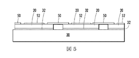
次に、描かれているように、パターン化絶縁層50が各圧電素子20の上面の上に形成されることが可能である。絶縁層50は、圧電素子アレイ20の上面に位置合わせされ、被着されるパターン化事前形成ステンシルを含むことができる。別の実施形態では、絶縁層50は、各圧電素子20の上面を露出させるようにパターニングおよびエッチングされるブランケット層として形成されることが可能である。完成した絶縁層50は、約1μm〜約100μm厚、または約10μm〜約50 μmまたは約15μm〜約30μmであることができる。換言すれば、絶縁層50の上面は、各圧電素子20の上面の、約1μm〜約100μm、または約10μm〜約50 μmまたは約15μm〜約30μm上である。
A patterned insulating
絶縁層50が形成された後、図5に描かれているように、導体52が各圧電素子20の上面に被着されることができる。導体52は導電性ペースト、金属、合金、導電性エポキシ樹脂、または別の導体であることができ、スクリーン印刷、液滴散布、スプレー、スパッタリング、化学気相成長、他のような任意の適切な技術によって与えられることができる。一実施形態では、絶縁層50は、隣接する圧電素子20同士の電気的短絡の可能性を低減するために、各圧電素子20の上面にわたる、一定量の流動可能な導体52の流れを含むことができる。
After the insulating
次に、フレックス回路60が図5の構造と、図6の拡大断面図に描かれているエンボス加工ダイのような整列したダイ62との間に入れられる。さまざまな設計のフレックス回路60が企図される。一実施形態では、フレックス回路60は、第1の誘電体層68(すなわち、はんだマスク)と第2の誘電体層70との間に入れられる複数の配線66によって連続するパッド64のアレイを含むことができる。
Next,
整列したダイ62は、パターン化バンプ72の適切なアレイを形成するように化学エッチングまたは選択的にメッキされる、金属、例えば316Lステンレス鋼のような任意の適切な剛体材料から形成されることができる。整列したダイ62の材料は、スタックプレス内で材料に課される圧力および熱に耐えるのに十分であるべきである。整列したダイ62として十分に機能し得る他の材料は、成型プラスチック、樹脂、ナイロン、他のような二次材料を含んでもよい。 The aligned dies 62 may be formed from any suitable rigid material, such as a metal, eg, 316L stainless steel, that is chemically etched or selectively plated to form a suitable array of patterned bumps 72. it can. The material of the aligned die 62 should be sufficient to withstand the pressure and heat imposed on the material in the stack press. Other materials that may function satisfactorily as aligned dies 62 may include secondary materials such as molded plastic, resin, nylon, etc.
一実施形態では、フレックス回路60はスタックプレス内で図5の構造体と整列したダイ62との間に入れられる。スタックプレスは底板74と上板76とを含むことができる。別の実施形態において、押圧が整列したダイ62の表面にわたって均一に分散されることを保証することを助けるために、対応するボンディングパッド78が整列したダイ62とスタックプレス上板76との間に配置されることができる。
In one embodiment, the
図5の構造体、フレックス回路60、および整列したダイ62が図6に描かれているようにスタックプレス内に配置されると、十分な圧力が整列したダイ62に加えられて、図7に描かれているようにフレックス回路を変形(すなわち、形成または成形)する。図7は、整列したダイ62を除去する前で、かつスタックプレスから除去された後であり、使用される場合は対応するパッド78が除去された後である、フレックス回路60の付着および変形後の図5の構造体を描いている。プレスによって与えられた圧力はフレックス回路パッド64のアレイを偏向させ、フレックス回路設計に応じて、描かれているように配線66を変形させることができる。一実施形態では、フレックス回路60をエンボス加工するために、約25psi〜約300psiの圧力が整列したダイ62に加えられることができる。圧力が不十分であると、フレックス回路64のエンボス加工が不十分な結果になる可能性があり、パッド64と圧電素子20との間で電気的な開状態が生じる可能性があり、一方で過剰な圧力は圧電素子20または他のジェットスタック機構を損傷する可能性がある。
When the structure of FIG. 5,
プレス内で圧力を加えている間、使用される導体に応じて、導体52を硬化させるために熱が加えられることができる。別の実施形態において、導体52はプレス内にある間に加熱および冷却されることができ、例えば、導体が金属はんだである場合、フレックス回路パッド64のトランスデューサ20に対する電気的結合がもたらされる。さらに別の実施形態において、導体52はフレックス回路60がプレスから除去された後に加熱および/または硬化されることができる。
While applying pressure in the press, depending on the conductor used, heat can be applied to cure the
続いて、整列したダイ62が除去され、図8に描かれているものに類似する構造体がもたらされる。この実施形態において、導体52は各フレックス回路パッド64と圧電素子20との間の電気的結合を促進することができる。加えて、フレックス回路がその元のより平坦な形状に戻る傾向を有する場合、導体は各フレックス回路パッド64を圧電素子20のうちの1つと電気的に接触したままに固定することができる。
Subsequently, the aligned die 62 is removed, resulting in a structure similar to that depicted in FIG. In this embodiment, the
次に、デバイスの設計に応じて追加の処理を実行することができる。追加の処理は例えば、導電性、誘電体、パターン化、または連続であることができ、図9に描かれているもののような層90によって共に概略的に表されている1つまたは複数の追加の層の形成を含むことができる。
Then, additional processing can be performed depending on the device design. The additional processing can be, for example, conductive, dielectric, patterned, or continuous, and one or more additional that are schematically represented together by a
次に、ジェット・スタック・サブアセンブリ30の設計に応じて、ジェットスタックを完成させるためにさまざまな処理工程が実行されることができる。例えば、1つまたは複数のインクポート開口92が図9に描かれているもののような層90を貫通して形成されることができる。さらに、デバイスの設計に応じて、インクポート開口92は、その開口92が電気的な開状態または他の望ましくない効果をもたらさない限り、フレックス回路60の一部を貫通して形成されることができる。インクポート開口92が描かれている場所に形成される場合、開口92はジェット・スタック・サブアセンブリを貫通して、例えば、ジェット・スタック・ダイヤフラムを貫通して延在することができる。別の実施形態では、フレックス回路60および/または圧電アレイ20が存在していない、描かれていない場所に1つまたは複数のインクポート開口が形成されてもよい。一実施形態では、図9に描かれているように、有孔プレート94が接着材(単純化するために個別に描かれてはいない)を用いてジェット・スタック・サブアセンブリ30に付着されることができる。有孔プレート94は、印刷中にインクが通って放出される複数のノズル96を含むことができる。有孔プレート94が付着されると、ジェットスタック98は完成する。ジェットスタック98は、単純化するために図示または説明されていない他の層、他の設計、他の開口、および追加の処理要件を含むことができる。
Next, depending on the design of the
次に、マニホールド100がジェットスタック98の上面に接着されることができ、これはマニホールド100をジェットスタック98に物理的に付着させる。マニホールド100の付着は、接着材等の流体密封シール式接続部102を使用することを含むことができ、結果的に図10に描かれているようなインク・ジェット・プリント・ヘッド104が生じる。インク・ジェット・プリント・ヘッド104は、マニホールド100の表面及びジェットスタック98の上面によって形成される、一定量のインクを貯蔵するためのインクリザーバ106を含むことができる。リザーバ106からのインクはポート92を通じてジェットスタック98に送達され、インクポートは部分的に、任意の上に重なる層90、フレックス回路60、絶縁層50、およびジェット・スタック・サブアセンブリ30を貫通する連続的な開口によって提供される。図10が簡易図であることは、理解されるであろう。実際のプリントヘッドは、図10には描かれていない、例えば左右への追加的構造体である様々な構造体及び差異を含んでもよいが、これらは、説明を単純にするために描画を省かれている。図10は2つのポート92を描いているが、600DPIジェットスタックは3つ以上のポートを含み得る。
Next, the manifold 100 can be adhered to the top surface of the
使用に際して、プリントヘッド104のマニホールド100内のリザーバ106は、一定量のインクを含む。プリントヘッドの最初のプライミングは、インクをリザーバ106からポート92を介してジェットスタック98内へと流れ込ませるために使用されることが可能である。フレックス回路パッドアレイのパッド64、導体52、および圧電電極20に伝達される、各配線66に加えられる電圧112に応答して、各PZT圧電素子20はそれに応じて適切な時点において曲がるかまたは偏向する。圧電素子20の偏向はジェットスタック98の一部であるダイヤフラム(個別には描かれていない)を屈曲させ、これによりジェットスタック内に圧力パルスが生じ、インクの一滴がノズル96から放出される。
In use, the
これにより、上述の方法及び構造体は、インク・ジェット・プリンタのためのジェットスタック98を形成する。一実施形態では、ジェットスタック98は、図11に描かれているようなインク・ジェット・プリント・ヘッド120の一部として使用されることが可能である。
Thus, the method and structure described above forms a
図11は、本教示の一実施形態による、1つまたは複数のプリントヘッド104および1つまたは複数のノズル96から噴出されるインク122を含むプリンタ120を描いたものである。各プリントヘッド104は、用紙、プラスチック、他のような印刷媒体124上へ所望される画像を生成するために、デジタル命令に従って動作するように構成される。各プリントヘッド104は、スワス毎に印刷画像を生成するために、走査動作において印刷媒体124に対して前後に移動することができる。代替的には、プリントヘッド104が固定して保持されかつ印刷媒体124がそれと相対的に移動されて、単一の通過でプリントヘッド104と同じ幅の画像が生成されてもよい。プリントヘッド104は、印刷媒体124より狭い、またはこれと同幅であることが可能である。プリンタハードウェアはプリンタハウジング126内に封入されることができる。別の実施形態では、プリントヘッドは、印刷媒体への後続の転写のために回転ドラムまたはベルトのような中間表面に印刷することができる。
FIG. 11 depicts a
図12Aおよび12Bに描かれているもののような代替の実施形態では、導体は使用されず、粗表面の接触による電気接触が確立される。この実施形態では、図6に描かれているもののようなフレックス回路60は、パッド64および圧電素子20が、図12A、12Bの拡大図に描かれているような複数の表面凹凸を含むように形成されることができる。複数のフレックス回路パッド64上の凹凸は、パッド64がそれらから形成される1つまたは複数の材料の自然な表面の粗さとして形成されることができ、1.0μm未満〜約3.0μmの平均高さを有することができる。続いて、図13に描かれているように、上述のような整列したダイ62が使用されてフレックス回路パッド64がエンボス加工される。この実施形態では、追加の導体はパッド64と圧電素子20との間に入れられない。フレックス回路パッド64上の表面凹凸と圧電素子20上の表面凹凸との間の物理接触に依拠して、パッド64と圧電素子20との間の電気的結合および電気的連通の確立が提供される。すなわち、複数のフレックス回路パッド64と複数の圧電素子20との間の導電性パスは、2つ表面の間の直接の物理接触によって提供される。
In alternative embodiments, such as those depicted in FIGS. 12A and 12B, no conductor is used and electrical contact is established by rough surface contact. In this embodiment, a
図13はさらに、本教示の実施形態のいずれかとともに使用されることができる任意選択の材料130の使用を描いたものである。例えば、高い応力が塑性変形を引き起こしていない場合、または降伏力に達していない場合、エポキシ樹脂または接着材のような任意選択の材料130は、可逆変形を回避するために、かつパッド64と圧電素子20との間の電気接触を維持するためにアクチュエータ20の上面の上で使用されることができる。任意選択の材料130は、図13に描かれているもののようなエンボス加工処理から生じる、フレックス回路60内のくぼみまたはディンプル内にのみ形成されることができる。別の実施形態では、材料130は、図8の構造体の上面全体にわたって形成されることができ、従って、図9における層90のそれと類似の形態をとることができる。
FIG. 13 further depicts the use of an
別の代替の実施形態では、図5〜10に描かれているもののような材料52は、接着材として使用され、かつ導体としては使用されない非導電材料であることができる。材料は例えば、非導電性エポキシ樹脂であることができる。材料52が不導体である実施形態では、電気接触は上述のような粗表面の接触によって確立されることができ、不導体は、例えばプリントヘッドの電気的動作の間に、エンボス加工されたフレックス回路パッド64を圧電素子20と電気接触したままに物理的に固定するであろう。別の実施形態では、非導電材料52は図13を参照して記載されるように任意選択の材料130とともに使用されることができる。
In another alternative embodiment,
本教示の別の実施形態が図14〜16に描かれている。この実施形態では、フレックス回路を形成するために整列したダイは使用されず、図14の拡大断面図に描かれているもののような対応するパッド140が使用される。対応するパッドは、約500μm〜約20ミリメートル(mm)厚、または約2mm〜約10mm厚、または約6mm〜約7mm厚のシリコーンの層であることができる。パッドが過剰に厚いと、フレックス回路パッドを形成するために変形させるための過剰な圧力が必要になるであろうし、パッドが過剰に薄いと、十分に変形せず、従ってフレックス回路を形成しないであろう。図6の実施形態と同様に、このアセンブリは、図14に描かれているもののような底板74および上板76を含むことができるスタックプレス内に配置されることができる。プレスによって、約5psi〜約500psi、または約10psi〜約450psi、または約25psi〜約400psiの範囲内の圧力がアセンブリに印加されることができ、これは対応するパッド140にフレックス回路にわたって均一な圧力を印加させる。圧力が不十分であると、フレックス回路64のエンボス加工が不十分な結果になる可能性があり、パッド64と圧電素子20との間で電気的な開状態が生じる可能性があり、一方で過剰な圧力は圧電素子20または他のジェットスタック機構を損傷する可能性がある。スタックプレス内で対応するパッドに圧力を印加している間、対応するパッド140は変形して、図15に描かれているように各アクチュエータ20の上の支持されていない領域に入り込み、フレックス回路パッド64をエンボス加工する。図16は、スタックプレスから除去された後で、かつ対応するパッド140を除去した後の図15のジェットスタック構造体を描いている。この実施形態では、バンプ電極64のアレイと圧電素子20のアレイとの間の電気接触が、図12Aおよび12Bに描かれているもののような粗表面の接触によって確立されることができるか、または別個の導体が使用されることができる。
Another embodiment of the present teachings is depicted in FIGS. In this embodiment, aligned dies are not used to form the flex circuit, and
図14〜16の実施形態では、スタックプレス内の圧力下で対応するパッドが自己整合を提供するとともに、偏向して圧電素子の各々の上の圧力のより低い、支持されていない領域内に入り込むため、整列したダイのフレックス回路および圧電素子アレイへの位置的不整合が回避される。 In the embodiment of FIGS. 14-16, the corresponding pad provides self-alignment under pressure in the stack press and deflects into the lower unsupported regions on each of the piezoelectric elements. Thus, positional misalignment of the aligned dies to the flex circuit and the piezoelectric element array is avoided.
従って、本明細書に記載されている本教示の様々な実施形態は、プリントヘッドの製造中の、フレックス回路の圧電素子アレイへの付着の間に複数のフレックス回路をin situでエンボス加工することによって、コストを低減することができる。本教示の様々な実施形態は、接合中にコンタクトパッド領域内で変形を引き起こすために局部的に応力の高い領域を生成する。本教示の実施形態では、フレックス回路の製造中の、別個の形成の間ではなく、フレックス回路のトランスデューサアレイへの電気的結合の間にフレックス回路が物理的に形成されるため、コストが低減されることができる。 Accordingly, various embodiments of the present teachings described herein emboss a plurality of flex circuits in situ during attachment of the flex circuit to the piezoelectric element array during printhead manufacture. Thus, the cost can be reduced. Various embodiments of the present teachings create locally stressed areas to cause deformation in the contact pad area during bonding. Embodiments of the present teachings reduce costs because the flex circuit is physically formed during electrical coupling to the transducer array of the flex circuit rather than during separate formation during manufacture of the flex circuit. Can.
Claims (5)
複数の圧電素子を備えるジェット・スタック・サブアセンブリをプレス内に配置することと、
パターン化バンプのアレイを含むダイを、フレックス回路とプレス板との間に配置することと、
ボンディングパッドを、前記ダイと前記プレス板との間に配置することと、
フレキシブルプリント回路(フレックス回路)の平坦で、エンボス加工されていない複数の導電性パッドを前記複数の圧電素子と位置合わせすることであって、前記平坦で、エンボス加工されていない複数の導電性パッドは、複数のフレックス回路の配線と連続し、複数のフレックス回路の配線と同じ導体層から形成される、ことと、
前記平坦で、エンボス加工されていない複数の導電性パッドを、起伏のある、エンボス加工された複数の導電性パッドに変形させるために前記プレス内で前記ダイとの接触を通じて前記フレックス回路に圧力を印加することと、を含み、前記プレス内の前記平坦で、エンボス加工されていない複数の導電性パッドの変形中、前記起伏のある、エンボス加工された複数の導電性パッドと前記複数の圧電素子との間に電気接触が確立される、方法。 A method for forming an ink jet print head comprising:
Placing a jet stack subassembly comprising a plurality of piezoelectric elements in a press;
The containing waste Lee an array of patterned bumps, and be disposed between the flex circuit and the press plate,
The Bonn loading pad, and positioning between the pressing plate and the die,
Aligning a plurality of flat, unembossed conductive pads of a flexible printed circuit (flex circuit) with the plurality of piezoelectric elements, the plurality of flat, non-embossed conductive pads Is formed from the same conductor layer as the wiring of the plurality of flex circuits, and is continuous with the wiring of the plurality of flex circuits.
The flat, a plurality of conductive pads that are not embossed, undulating, the flex circuit through contact with front Kida Lee in the press in order to deform the plurality of conductive pads embossed Applying pressure, and during deformation of the flat, unembossed conductive pads in the press, the undulating, embossed conductive pads and the plurality of conductive pads A method wherein electrical contact is established with a piezoelectric element.
前記プレス内での前記フレックス回路への圧力の前記印加の間に、前記エンボス加工された複数の導電性パッドの各々を各圧電素子の前記表面上の前記導体と接触させることと、をさらに含み、
前記複数の導電性パッドおよび前記複数の圧電素子による前記導体の接触を通じて前記エンボス加工されていない複数の導電性パッドと前記複数の圧電素子との間で電気接触が確立される、請求項1に記載の方法。 Attaching a conductor to the surface of each piezoelectric element of the plurality of piezoelectric elements;
Contacting each of the plurality of embossed conductive pads with the conductor on the surface of each piezoelectric element during the application of pressure to the flex circuit within the press. ,
The electrical contact is established between the plurality of unembossed conductive pads and the plurality of piezoelectric elements through contact of the conductors with the plurality of conductive pads and the plurality of piezoelectric elements. The method described.
前記複数の圧電素子の各圧電素子の表面に非導電材料を付着させることと、
前記プレス内の前記フレックス回路への圧力の前記印加の間に前記起伏のある、エンボス加工された複数の導電性パッドの各々を各圧電素子の前記表面上の前記非導電材料と接触させることと、
前記起伏のある、エンボス加工された複数の導電性パッドの各々との接触中に前記非導電材料を硬化させることと、をさらに含み、前記硬化した非導電材料は、前記起伏のある、エンボス加工された複数の導電性パッドの各々と前記複数の圧電素子との間の物理接触を維持する、請求項1に記載の方法。 Before placing the jet stack subassembly in the press,
Attaching a non-conductive material to the surface of each piezoelectric element of the plurality of piezoelectric elements;
Contacting each of the undulating, embossed conductive pads with the non-conductive material on the surface of each piezoelectric element during the application of pressure to the flex circuit in the press; ,
Curing the non-conductive material during contact with each of the undulating, embossed conductive pads, wherein the hardened non-conductive material is the undulating embossing The method of claim 1, wherein physical contact is maintained between each of the plurality of conductive pads formed and the plurality of piezoelectric elements.
複数の圧電素子を備えるジェット・スタック・サブアセンブリをプレス内に配置することと、
パターン化バンプのアレイを含むダイを、フレックス回路とプレス板との間に配置することと、
ボンディングパッドを、前記ダイと前記プレス板との間に配置することと、
フレキシブルプリント回路(フレックス回路)の平坦で、エンボス加工されていない複数の導電性パッドを前記複数の圧電素子と位置合わせすることであって、前記平坦で、エンボス加工されていない複数の導電性パッドは、複数のフレックス回路の配線と連続し、複数のフレックス回路の配線と同じ導体層から形成される、ことと、
前記平坦で、エンボス加工されていない複数の導電性パッドを、起伏のある、エンボス加工された複数の導電性パッドに変形させるために前記プレス内で前記ダイとの接触を通じて前記フレックス回路に圧力を印加することと、を含み、前記プレス内の前記平坦で、エンボス加工されていない複数の導電性パッドの変形中、前記起伏のある、エンボス加工された複数の導電性パッドと前記複数の圧電素子との間に電気接触が確立される方法を使用してインク・ジェット・プリント・ヘッドを形成することと、
前記プリントヘッドをプリンタハウジング内に封入することと、を含む、方法。 A method for forming a printer comprising:
Placing a jet stack subassembly comprising a plurality of piezoelectric elements in a press;
The containing waste Lee an array of patterned bumps, and be disposed between the flex circuit and the press plate,
The Bonn loading pad, and positioning between the pressing plate and the die,
Aligning a plurality of flat, unembossed conductive pads of a flexible printed circuit (flex circuit) with the plurality of piezoelectric elements, the plurality of flat, non-embossed conductive pads Is formed from the same conductor layer as the wiring of the plurality of flex circuits, and is continuous with the wiring of the plurality of flex circuits.
The flat, a plurality of conductive pads that are not embossed, undulating, the flex circuit through contact with front Kida Lee in the press in order to deform the plurality of conductive pads embossed Applying pressure, and during deformation of the flat, unembossed conductive pads in the press, the undulating, embossed conductive pads and the plurality of conductive pads Forming an ink jet print head using a method in which electrical contact is established with a piezoelectric element;
Encapsulating the print head in a printer housing.
Applications Claiming Priority (2)
| Application Number | Priority Date | Filing Date | Title |
|---|---|---|---|
| US13/232,465 US8584331B2 (en) | 2011-09-14 | 2011-09-14 | In situ flexible circuit embossing to form an electrical interconnect |
| US13/232,465 | 2011-09-14 |
Publications (3)
| Publication Number | Publication Date |
|---|---|
| JP2013060008A JP2013060008A (en) | 2013-04-04 |
| JP2013060008A5 JP2013060008A5 (en) | 2015-10-08 |
| JP5934058B2 true JP5934058B2 (en) | 2016-06-15 |
Family
ID=47828541
Family Applications (1)
| Application Number | Title | Priority Date | Filing Date |
|---|---|---|---|
| JP2012184354A Expired - Fee Related JP5934058B2 (en) | 2011-09-14 | 2012-08-23 | In situ flexible circuit embossing to form electrical interconnects |
Country Status (3)
| Country | Link |
|---|---|
| US (1) | US8584331B2 (en) |
| JP (1) | JP5934058B2 (en) |
| CN (1) | CN102991136B (en) |
Families Citing this family (5)
| Publication number | Priority date | Publication date | Assignee | Title |
|---|---|---|---|---|
| US8628173B2 (en) * | 2010-06-07 | 2014-01-14 | Xerox Corporation | Electrical interconnect using embossed contacts on a flex circuit |
| US9079392B2 (en) * | 2013-09-26 | 2015-07-14 | Xerox Corporation | Double sided flex for improved bump interconnect |
| US10038267B2 (en) * | 2014-06-12 | 2018-07-31 | Palo Alto Research Center Incorporated | Circuit interconnect system and method |
| US10797421B2 (en) * | 2018-05-23 | 2020-10-06 | Xerox Corporation | Landing electrical contact |
| US10813225B2 (en) * | 2019-02-15 | 2020-10-20 | Xerox Corporation | Radio-frequency identification (RFID) label or conductive trace thermal transfer printing method |
Family Cites Families (14)
| Publication number | Priority date | Publication date | Assignee | Title |
|---|---|---|---|---|
| JPH05169655A (en) * | 1991-12-26 | 1993-07-09 | Seiko Epson Corp | Ink jet recording head and its manufacturing method |
| DE69710240T2 (en) * | 1996-04-10 | 2002-06-27 | Seiko Epson Corp | Ink jet recording head |
| JPH10112584A (en) * | 1996-10-04 | 1998-04-28 | Seiko Epson Corp | Connecting method for circuit board, connecting structure for circuit board, and liquid crystal device using the structure |
| US6464324B1 (en) * | 2000-01-31 | 2002-10-15 | Picojet, Inc. | Microfluid device and ultrasonic bonding process |
| JP4362996B2 (en) * | 2001-08-22 | 2009-11-11 | 富士ゼロックス株式会社 | Piezoelectric / electrostrictive actuator having lattice arrangement and manufacturing method thereof |
| JP2003124256A (en) * | 2001-10-12 | 2003-04-25 | Matsushita Electric Ind Co Ltd | Mounting method of flexible substrate |
| JP3906225B2 (en) * | 2002-11-27 | 2007-04-18 | 住友ベークライト株式会社 | Circuit board, multilayer wiring board, method for manufacturing circuit board, and method for manufacturing multilayer wiring board |
| TWI263403B (en) * | 2004-01-22 | 2006-10-01 | Murata Manufacturing Co | Electronic component manufacturing method |
| JP4628067B2 (en) * | 2004-11-12 | 2011-02-09 | 株式会社 ハリーズ | Interposer joining method and electronic component. |
| JP4661228B2 (en) * | 2005-01-13 | 2011-03-30 | セイコーエプソン株式会社 | Droplet discharge head and droplet discharge apparatus |
| JP4497053B2 (en) * | 2005-08-15 | 2010-07-07 | セイコーエプソン株式会社 | Device mounting structure, liquid discharge head, liquid discharge apparatus, electronic device, and electronic apparatus |
| JP5074789B2 (en) * | 2007-03-06 | 2012-11-14 | 住友電気工業株式会社 | Connection structure |
| JP2009096851A (en) * | 2007-10-15 | 2009-05-07 | Three M Innovative Properties Co | Nonconductive adhesive composition, nonconductive adhesive film, and methods for production and use thereof |
| JP2010225732A (en) * | 2009-03-23 | 2010-10-07 | Seiko Epson Corp | Liquid droplet ejection head, and liquid droplet ejection device |
-
2011
- 2011-09-14 US US13/232,465 patent/US8584331B2/en active Active
-
2012
- 2012-08-23 JP JP2012184354A patent/JP5934058B2/en not_active Expired - Fee Related
- 2012-09-06 CN CN201210328054.1A patent/CN102991136B/en not_active Expired - Fee Related
Also Published As
| Publication number | Publication date |
|---|---|
| CN102991136B (en) | 2015-08-26 |
| CN102991136A (en) | 2013-03-27 |
| US20130061469A1 (en) | 2013-03-14 |
| US8584331B2 (en) | 2013-11-19 |
| JP2013060008A (en) | 2013-04-04 |
Similar Documents
| Publication | Publication Date | Title |
|---|---|---|
| US9381737B2 (en) | Method of manufacturing a print head | |
| JP5934058B2 (en) | In situ flexible circuit embossing to form electrical interconnects | |
| EP1657059B1 (en) | Piezoelectric actuator, method for manufacturing piezoelectric actuator, and liquid transporting apparatus | |
| JP5793095B2 (en) | Method for forming an inkjet printhead | |
| US7891093B2 (en) | Method for manufacturing an inkjet head | |
| JP4134773B2 (en) | Inkjet head | |
| JP4281608B2 (en) | Recording head manufacturing method and recording head | |
| JP4899678B2 (en) | Liquid transfer device, actuator unit, and method of manufacturing liquid transfer device | |
| JP2009078564A (en) | Method of manufacturing recording head, and recording head | |
| JP4887747B2 (en) | Piezoelectric actuator, method for manufacturing piezoelectric actuator, and liquid transfer device | |
| JP5886723B2 (en) | Bonded silicon structures for high density printheads | |
| JP2006116953A (en) | Liquid ejecting apparatus and manufacturing method therefor | |
| US20060170737A1 (en) | Ink-Jet Head | |
| WO2001042024A1 (en) | Ink jet head and printer | |
| US7815293B2 (en) | Ink-jet head and method of producing the same | |
| JP4634118B2 (en) | Inkjet device | |
| CN107303757B (en) | Method of forming piezoelectric actuator electrode | |
| JPH09300609A (en) | Ink-jet head | |
| JP2013067166A (en) | High density electrical interconnect using limited density flex circuits | |
| JP2006082393A (en) | Ink-jet recording head and ink-jet printer | |
| JP2004160942A (en) | Ink jet head and its manufacturing process | |
| JP3656800B2 (en) | Ink jet recording apparatus and manufacturing method thereof | |
| JP2010012724A (en) | Liquid droplet discharge head, image forming apparatus, and method for manufacturing liquid droplet discharge head | |
| US20170320324A1 (en) | Inkjet head and printer | |
| US8205969B2 (en) | Jet stack with precision port holes for ink jet printer and associated method |
Legal Events
| Date | Code | Title | Description |
|---|---|---|---|
| RD04 | Notification of resignation of power of attorney |
Free format text: JAPANESE INTERMEDIATE CODE: A7424 Effective date: 20131212 |
|
| A521 | Written amendment |
Free format text: JAPANESE INTERMEDIATE CODE: A523 Effective date: 20150821 |
|
| A621 | Written request for application examination |
Free format text: JAPANESE INTERMEDIATE CODE: A621 Effective date: 20150821 |
|
| A871 | Explanation of circumstances concerning accelerated examination |
Free format text: JAPANESE INTERMEDIATE CODE: A871 Effective date: 20150821 |
|
| A975 | Report on accelerated examination |
Free format text: JAPANESE INTERMEDIATE CODE: A971005 Effective date: 20150930 |
|
| A131 | Notification of reasons for refusal |
Free format text: JAPANESE INTERMEDIATE CODE: A131 Effective date: 20151027 |
|
| A521 | Written amendment |
Free format text: JAPANESE INTERMEDIATE CODE: A523 Effective date: 20160105 |
|
| A131 | Notification of reasons for refusal |
Free format text: JAPANESE INTERMEDIATE CODE: A131 Effective date: 20160209 |
|
| A521 | Written amendment |
Free format text: JAPANESE INTERMEDIATE CODE: A523 Effective date: 20160325 |
|
| TRDD | Decision of grant or rejection written | ||
| A01 | Written decision to grant a patent or to grant a registration (utility model) |
Free format text: JAPANESE INTERMEDIATE CODE: A01 Effective date: 20160426 |
|
| A61 | First payment of annual fees (during grant procedure) |
Free format text: JAPANESE INTERMEDIATE CODE: A61 Effective date: 20160506 |
|
| R150 | Certificate of patent or registration of utility model |
Ref document number: 5934058 Country of ref document: JP Free format text: JAPANESE INTERMEDIATE CODE: R150 |
|
| R250 | Receipt of annual fees |
Free format text: JAPANESE INTERMEDIATE CODE: R250 |
|
| R250 | Receipt of annual fees |
Free format text: JAPANESE INTERMEDIATE CODE: R250 |
|
| LAPS | Cancellation because of no payment of annual fees |