JP5910806B2 - Optical module and atomic oscillator for an atomic oscillator - Google Patents
Optical module and atomic oscillator for an atomic oscillator Download PDFInfo
- Publication number
- JP5910806B2 JP5910806B2 JP2011055432A JP2011055432A JP5910806B2 JP 5910806 B2 JP5910806 B2 JP 5910806B2 JP 2011055432 A JP2011055432 A JP 2011055432A JP 2011055432 A JP2011055432 A JP 2011055432A JP 5910806 B2 JP5910806 B2 JP 5910806B2
- Authority
- JP
- Japan
- Prior art keywords
- light
- optical filter
- substrate
- atomic oscillator
- incident
- Prior art date
- Legal status (The legal status is an assumption and is not a legal conclusion. Google has not performed a legal analysis and makes no representation as to the accuracy of the status listed.)
- Active
Links
- 230000003287 optical effect Effects 0.000 title claims description 198
- 239000004065 semiconductor Substances 0.000 claims description 80
- 239000000758 substrate Substances 0.000 claims description 52
- 150000001340 alkali metals Chemical class 0.000 claims description 31
- 229910052783 alkali metal Inorganic materials 0.000 claims description 22
- 239000002585 base Substances 0.000 claims description 16
- 230000000694 effects Effects 0.000 claims description 15
- 239000000463 material Substances 0.000 claims description 12
- BJQHLKABXJIVAM-UHFFFAOYSA-N bis(2-ethylhexyl) phthalate Chemical compound CCCCC(CC)COC(=O)C1=CC=CC=C1C(=O)OCC(CC)CCCC BJQHLKABXJIVAM-UHFFFAOYSA-N 0.000 claims description 11
- 150000001875 compounds Chemical class 0.000 claims description 8
- 239000010410 layer Substances 0.000 description 83
- 230000008859 change Effects 0.000 description 12
- 238000001514 detection method Methods 0.000 description 12
- 238000010586 diagram Methods 0.000 description 8
- 229910001218 Gallium arsenide Inorganic materials 0.000 description 7
- 230000005699 Stark effect Effects 0.000 description 7
- 238000004519 manufacturing process Methods 0.000 description 7
- 230000005684 electric field Effects 0.000 description 6
- 229910000980 Aluminium gallium arsenide Inorganic materials 0.000 description 4
- 229910004298 SiO 2 Inorganic materials 0.000 description 4
- 230000007423 decrease Effects 0.000 description 4
- 230000007613 environmental effect Effects 0.000 description 4
- 238000005215 recombination Methods 0.000 description 4
- 230000006798 recombination Effects 0.000 description 4
- 238000001228 spectrum Methods 0.000 description 4
- 230000005284 excitation Effects 0.000 description 3
- 239000000835 fiber Substances 0.000 description 3
- 230000004888 barrier function Effects 0.000 description 2
- TVFDJXOCXUVLDH-UHFFFAOYSA-N caesium atom Chemical compound [Cs] TVFDJXOCXUVLDH-UHFFFAOYSA-N 0.000 description 2
- 230000001427 coherent effect Effects 0.000 description 2
- 239000012535 impurity Substances 0.000 description 2
- 230000031700 light absorption Effects 0.000 description 2
- 238000012986 modification Methods 0.000 description 2
- 230000004048 modification Effects 0.000 description 2
- 239000013307 optical fiber Substances 0.000 description 2
- 230000010355 oscillation Effects 0.000 description 2
- SBIBMFFZSBJNJF-UHFFFAOYSA-N selenium;zinc Chemical compound [Se]=[Zn] SBIBMFFZSBJNJF-UHFFFAOYSA-N 0.000 description 2
- 239000011734 sodium Substances 0.000 description 2
- 239000000126 substance Substances 0.000 description 2
- 238000002834 transmittance Methods 0.000 description 2
- DGAQECJNVWCQMB-PUAWFVPOSA-M Ilexoside XXIX Chemical compound C[C@@H]1CC[C@@]2(CC[C@@]3(C(=CC[C@H]4[C@]3(CC[C@@H]5[C@@]4(CC[C@@H](C5(C)C)OS(=O)(=O)[O-])C)C)[C@@H]2[C@]1(C)O)C)C(=O)O[C@H]6[C@@H]([C@H]([C@@H]([C@H](O6)CO)O)O)O.[Na+] DGAQECJNVWCQMB-PUAWFVPOSA-M 0.000 description 1
- 238000010521 absorption reaction Methods 0.000 description 1
- 230000009471 action Effects 0.000 description 1
- 229910052792 caesium Inorganic materials 0.000 description 1
- 239000000969 carrier Substances 0.000 description 1
- 238000005253 cladding Methods 0.000 description 1
- 239000012792 core layer Substances 0.000 description 1
- 230000005686 electrostatic field Effects 0.000 description 1
- 230000003993 interaction Effects 0.000 description 1
- 229910052751 metal Inorganic materials 0.000 description 1
- 239000002184 metal Chemical group 0.000 description 1
- 230000005693 optoelectronics Effects 0.000 description 1
- 230000000737 periodic effect Effects 0.000 description 1
- 239000012466 permeate Substances 0.000 description 1
- 238000002310 reflectometry Methods 0.000 description 1
- 229910052701 rubidium Inorganic materials 0.000 description 1
- IGLNJRXAVVLDKE-UHFFFAOYSA-N rubidium atom Chemical compound [Rb] IGLNJRXAVVLDKE-UHFFFAOYSA-N 0.000 description 1
- 239000002356 single layer Substances 0.000 description 1
- 229910052708 sodium Inorganic materials 0.000 description 1
- 230000003595 spectral effect Effects 0.000 description 1
Images


Classifications
-
- H—ELECTRICITY
- H03—ELECTRONIC CIRCUITRY
- H03L—AUTOMATIC CONTROL, STARTING, SYNCHRONISATION, OR STABILISATION OF GENERATORS OF ELECTRONIC OSCILLATIONS OR PULSES
- H03L7/00—Automatic control of frequency or phase; Synchronisation
- H03L7/26—Automatic control of frequency or phase; Synchronisation using energy levels of molecules, atoms, or subatomic particles as a frequency reference
-
- G—PHYSICS
- G04—HOROLOGY
- G04F—TIME-INTERVAL MEASURING
- G04F5/00—Apparatus for producing preselected time intervals for use as timing standards
- G04F5/14—Apparatus for producing preselected time intervals for use as timing standards using atomic clocks
- G04F5/145—Apparatus for producing preselected time intervals for use as timing standards using atomic clocks using Coherent Population Trapping
Landscapes
- Physics & Mathematics (AREA)
- Life Sciences & Earth Sciences (AREA)
- Ecology (AREA)
- General Physics & Mathematics (AREA)
- Spectroscopy & Molecular Physics (AREA)
- Semiconductor Lasers (AREA)
- Stabilization Of Oscillater, Synchronisation, Frequency Synthesizers (AREA)
- Optical Filters (AREA)
Description
本発明は、原子発振器用の光学モジュールおよび原子発振器に関する。 The present invention relates to an optical module for an atomic oscillator and an atomic oscillator.
近年、量子干渉効果のひとつであるCPT(Coherent Population Trapping)を利用した原子発振器が提案され、装置の小型化や低消費電力化が期待されている。CPTを利用した原子発振器は、アルカリ金属原子に互いに波長(周波数)の異なる2つの共鳴光を同時に照射すると、2つの共鳴光の吸収が停止する現象(EIT現象:Electromagnetically Induced Transparency)を利用した発振器である。例えば、特許文献1には、CPTを利用した原子発振器として、コヒーレントな光を発する光源と、アルカリ金属原子が封入されたガスセルと、ガスセルを透過した光の強度を検出する受光素子と、を有する光学モジュールを含んで構成された原子発振器が記載されている。 In recent years, atomic oscillators using CPT (Coherent Population Trapping), which is one of the quantum interference effects, have been proposed, and miniaturization of devices and low power consumption are expected. An atomic oscillator using a CPT is an oscillator using a phenomenon (EIT phenomenon: Electromagnetically Induced Transparency) in which absorption of two resonance lights is stopped simultaneously when two resonance lights having different wavelengths (frequencies) are simultaneously irradiated onto an alkali metal atom. It is. For example, Patent Document 1 includes, as an atomic oscillator using CPT, a light source that emits coherent light, a gas cell in which alkali metal atoms are sealed, and a light receiving element that detects the intensity of light transmitted through the gas cell. An atomic oscillator configured to include an optical module is described.
CPTを利用した原子発振器では、例えば、光源として半導体レーザーが用いられる。光源として半導体レーザーを用いた原子発振器では、例えば、半導体レーザーの駆動電流を変調することによって半導体レーザーから出射される光に側帯波を発生させて、EIT現象を発現させている。 In an atomic oscillator using CPT, for example, a semiconductor laser is used as a light source. In an atomic oscillator using a semiconductor laser as a light source, for example, a sideband is generated in the light emitted from the semiconductor laser by modulating the driving current of the semiconductor laser, thereby causing the EIT phenomenon.
しかしながら、駆動電流が変調された半導体レーザーから出射される光には、側帯波だけでなく、EIT現象に寄与しない中心波長を有する基本波(搬送波)も含まれる。この基本波がアルカリ金属原子に照射されると、アルカリ金属原子が吸収する光の波長(周波数)が変化して(ACシュタルク効果)、原子発振器の周波数の安定度を低下させる場合がある。 However, the light emitted from the semiconductor laser whose drive current is modulated includes not only the sideband wave but also a fundamental wave (carrier wave) having a center wavelength that does not contribute to the EIT phenomenon. When the alkali metal atom is irradiated with this fundamental wave, the wavelength (frequency) of the light absorbed by the alkali metal atom changes (AC Stark effect), which may reduce the frequency stability of the atomic oscillator.
本発明のいくつかの態様に係る目的の1つは、周波数安定度の高い原子発振器を得ることが可能な原子発振器用の光学モジュールを提供することにある。また、本発明のいくつかの態様に係る目的の1つは、上記原子発振器用の光学モジュールを有する原子発振器を提供することにある。 One of the objects according to some embodiments of the present invention is to provide an optical module for an atomic oscillator capable of obtaining an atomic oscillator with high frequency stability. Another object of some aspects of the present invention is to provide an atomic oscillator having the optical module for the atomic oscillator.
本発明に係る原子発振器用の光学モジュールは、
量子干渉効果を利用する原子発振器用の光学モジュールであって、
所定の波長を有する基本波、当該基本波の側帯波、を含む光を出射する光源と、
前記光源からの光が入射し、当該入射した光のうち前記側帯波を透過させる波長選択部と、
アルカリ金属ガスを封入し、前記波長選択部を透過した光が照射されるガスセルと、
前記ガスセルに照射された光のうち前記ガスセルを透過した光の強度を検出する光検出部と、
を含み、
前記波長選択部は、
所定の波長範囲の光を透過させる光フィルター部と、
前記光フィルター部が透過させる光の波長範囲を変化させる光フィルター特性制御部と、
を有する。
An optical module for an atomic oscillator according to the present invention,
An optical module for an atomic oscillator using the quantum interference effect,
A light source that emits light including a fundamental wave having a predetermined wavelength, and a sideband of the fundamental wave;
A wavelength selection unit that receives light from the light source and transmits the sideband of the incident light;
A gas cell in which an alkali metal gas is sealed and irradiated with light transmitted through the wavelength selection unit;
A light detector for detecting the intensity of light transmitted through the gas cell among the light irradiated to the gas cell;
Including
The wavelength selector is
An optical filter that transmits light in a predetermined wavelength range;
An optical filter characteristic control unit that changes a wavelength range of light transmitted by the optical filter unit;
Have
このような原子発振器用の光学モジュールによれば、波長選択部が、光源からの光に含まれる基本波の強度を減少または基本波を消滅させることができる。これにより、EIT現象に寄与しない基本波がアルカリ金属原子に照射されることを抑制または防止できる。したがって、ACシュタルク効果による周波数変動を抑制することができ、周波数安定度の高い発振器を提供できる。さらに、波長選択部が、光フィルター部が透過させる光の波長範囲を変化させる光フィルター特性制御部を有しているため、製造誤差や環境変化等による光フィルター部の波長選択特性(光フィルター部が透過させる光の波長範囲)のずれを補正することができる。 According to such an optical module for an atomic oscillator, the wavelength selection unit can reduce the intensity of the fundamental wave included in the light from the light source or eliminate the fundamental wave. Thereby, it can suppress or prevent that the fundamental wave which does not contribute to an EIT phenomenon is irradiated to an alkali metal atom. Therefore, frequency fluctuation due to the AC Stark effect can be suppressed, and an oscillator with high frequency stability can be provided. Furthermore, since the wavelength selection unit has an optical filter characteristic control unit that changes the wavelength range of the light transmitted by the optical filter unit, the wavelength selection characteristic (optical filter unit) of the optical filter unit due to manufacturing error, environmental change, etc. Can be corrected.
本発明に係る原子発振器用の光学モジュールにおいて、
前記光フィルター部は、エタロンであり、
前記光フィルター特性制御部は、電気光学効果によって、前記光フィルター部が透過させる光の波長範囲を変化させることができる。
In the optical module for an atomic oscillator according to the present invention,
The optical filter portion is an etalon,
The optical filter characteristic control unit can change a wavelength range of light transmitted by the optical filter unit by an electro-optic effect.
このような原子発振器用の光学モジュールによれば、光フィルター部を簡易な構成にすることができる。さらに、光フィルター部の波長選択特性を、高精度かつ容易に制御できる。 According to such an optical module for an atomic oscillator, the optical filter portion can be configured simply. Furthermore, the wavelength selection characteristic of the optical filter section can be controlled with high accuracy and ease.
本発明に係る原子発振器用の光学モジュールにおいて、
前記光フィルター部は、
前記波長選択部に入射した光を反射させ、互いに対向する第1ミラーおよび第2ミラーと、
前記第1ミラーと前記第2ミラーとの間に配置された基板と、
を有し、
前記基板の材質は、化合物半導体であることができる。
In the optical module for an atomic oscillator according to the present invention,
The optical filter section is
A first mirror and a second mirror that reflect the light incident on the wavelength selection unit and face each other;
A substrate disposed between the first mirror and the second mirror;
Have
The substrate may be a compound semiconductor.
このような原子発振器用の光学モジュールによれば、第1ミラーと第2ミラーとの間の距離を小さくでき、装置の小型化を図ることができる。 According to such an optical module for an atomic oscillator, the distance between the first mirror and the second mirror can be reduced, and the apparatus can be miniaturized.
本発明に係る原子発振器用の光学モジュールにおいて、
前記光フィルター特性制御部は、前記基板に電圧を印加する第1電極および第2電極を有することができる。
In the optical module for an atomic oscillator according to the present invention,
The optical filter characteristic control unit may include a first electrode and a second electrode that apply a voltage to the substrate.
このような原子発振器用の光学モジュールによれば、光フィルター特性制御部を簡易な構成にすることができる。 According to such an optical module for an atomic oscillator, the optical filter characteristic control unit can have a simple configuration.
本発明に係る原子発振器用の光学モジュールにおいて、
さらに、化合物半導体の基体を含み、
前記光源は、半導体レーザーであり、
前記光フィルター部および前記光源は、前記基体上に位置し、
前記第1電極は、前記基体の前記光フィルター部が位置する側と反対側に位置し、
前記第2電極は、前記光フィルター部の前記基体が位置する側と反対側に位置することができる。
In the optical module for an atomic oscillator according to the present invention,
In addition, a compound semiconductor substrate,
The light source is a semiconductor laser;
The light filter part and the light source are located on the base,
The first electrode is located on the opposite side of the base on which the optical filter portion is located,
The second electrode may be located on the opposite side of the optical filter portion from the side where the substrate is located.
このような原子発振器用の光学モジュールによれば、波長選択部および光源が同じ基体に形成されているため、装置の小型化を図ることができる。 According to such an optical module for an atomic oscillator, since the wavelength selection unit and the light source are formed on the same substrate, the apparatus can be miniaturized.
なお、本発明に係る記載では、「上方」という文言を、例えば、「特定のもの(以下、「A」という)の「上方」に他の特定のもの(以下、「B」という)を形成する」などと用いる場合に、A上に直接Bを形成するような場合と、A上に他のものを介してBを形成するような場合とが含まれるものとして、「上方」という文言を用いている。同様に、「下方」という文言は、A下に直接Bを形成するような場合と、A下に他のものを介してBを形成するような場合とが含まれるものとする。 In the description according to the present invention, the word “upper” is used, for example, “specifically” (hereinafter referred to as “A”) is formed above another specific thing (hereinafter referred to as “B”). The word “above” is used to include the case where B is formed directly on A and the case where B is formed on A via another object. Used. Similarly, the term “below” includes a case where B is directly formed under A and a case where B is formed under another through A.
本発明に係る原子発振器用の光学モジュールにおいて、
前記光フィルター部の前記基板は、前記基体側から積層された第1層、第2層、および第3層を有し、
前記第1層の屈折率および前記第3層の屈折率は、前記第2層の屈折率より小さく、
前記第2層は、前記光源から出射した光を伝播させることができる。
In the optical module for an atomic oscillator according to the present invention,
The substrate of the optical filter portion has a first layer, a second layer, and a third layer laminated from the base side,
The refractive index of the first layer and the refractive index of the third layer are smaller than the refractive index of the second layer,
The second layer can propagate light emitted from the light source.
このような原子発振器用の光学モジュールによれば、基板を光導波路とすることができる。したがって、波長選択部から射出される光のビーム径を制御することができ、波長選択部を透過した光をガスセルに効率よく照射することができる。 According to such an optical module for an atomic oscillator, the substrate can be an optical waveguide. Therefore, the beam diameter of the light emitted from the wavelength selection unit can be controlled, and the light transmitted through the wavelength selection unit can be efficiently irradiated onto the gas cell.
本発明に係る原子発振器用の光学モジュールにおいて、
前記光源は、端面発光型レーザーであることができる。
In the optical module for an atomic oscillator according to the present invention,
The light source may be an edge emitting laser.
このような原子発振器用の光学モジュールによれば、端面発光型レーザーを構成する層の膜厚の制御によって、光源(端面発光型レーザー)と波長選択部との間のアライメントができる。したがって、光源と波長選択部との間のアライメント精度を向上させることができる。さらに、例えば、波長選択部に光源からの光を入射させるための光学素子が不要となる。 According to such an optical module for an atomic oscillator, alignment between the light source (edge-emitting laser) and the wavelength selection unit can be performed by controlling the film thickness of the layer constituting the edge-emitting laser. Therefore, the alignment accuracy between the light source and the wavelength selector can be improved. Furthermore, for example, an optical element for making the light from the light source incident on the wavelength selection unit becomes unnecessary.
本発明に係る原子発振器用の光学モジュールにおいて、
前記光源は、面発光型レーザーであることができる。
In the optical module for an atomic oscillator according to the present invention,
The light source may be a surface emitting laser.
このような原子発振器用の光学モジュールによれば、面発光型レーザーは、端面発光型レーザーと比べて、ゲインを生じさせるための電流が少ないため、低消費電力化を図ることができる。 According to such an optical module for an atomic oscillator, the surface-emitting laser has a smaller current for generating a gain than the edge-emitting laser, so that the power consumption can be reduced.
本発明に係る原子発振器は、
本発明に係る原子発振器用の光学モジュールを含む。
The atomic oscillator according to the present invention is
An optical module for an atomic oscillator according to the present invention is included.
このような原子発振器は、本発明に係る原子発振器用の光学モジュールを含むため、ACシュタルク効果による周波数変動を抑制することができ、周波数安定度を高めることができる。 Since such an atomic oscillator includes the optical module for an atomic oscillator according to the present invention, frequency fluctuation due to the AC Stark effect can be suppressed and frequency stability can be increased.
本発明に係る原子発振器は、
量子干渉効果を利用する原子発振器用であって、
所定の波長を有する基本波、当該基本波の側帯波、を含む光を出射する光源と、
前記光源からの光が入射し、当該入射した光のうち前記側帯波を透過する波長選択部と、
アルカリ金属ガスを封入し、前記波長選択部を透過した光が照射されるガスセルと、
前記ガスセルに照射された光のうち前記ガスセルを透過した光の強度を検出する光検出部と、
を含み、
前記波長選択部は、
所定の波長範囲の光を選択して射出する光フィルター部と、
前記光フィルター部が選択する波長範囲を変化させる光フィルター特性制御部と、
を有する。
The atomic oscillator according to the present invention is
For atomic oscillators using quantum interference effects,
A light source that emits light including a fundamental wave having a predetermined wavelength, and a sideband of the fundamental wave;
A wavelength selection unit that receives light from the light source and transmits the sideband of the incident light;
A gas cell in which an alkali metal gas is sealed and irradiated with light transmitted through the wavelength selection unit;
A light detector for detecting the intensity of light transmitted through the gas cell among the light irradiated to the gas cell;
Including
The wavelength selector is
An optical filter unit for selecting and emitting light in a predetermined wavelength range;
An optical filter characteristic control unit that changes a wavelength range selected by the optical filter unit;
Have
このような原子発振器によれば、波長選択部が、光源からの光に含まれる基本波の強度を減少または基本波を消滅させることができる。これにより、EIT現象に寄与しない基本波がアルカリ金属原子に照射されることを抑制または防止できる。したがって、ACシュタルク効果による周波数変動を抑制することができ、周波数安定度の高い発振器を提供できる。さらに、波長選択部が、光フィルター部が透過させる光の波長範囲を変化させる光フィルター特性制御部を有しているため、製造誤差や環境変化等による光フィルター部の波長選択特性(光フィルター部が透過させる光の波長範囲)のずれを補正することができる。 According to such an atomic oscillator, the wavelength selection unit can reduce the intensity of the fundamental wave included in the light from the light source or eliminate the fundamental wave. Thereby, it can suppress or prevent that the fundamental wave which does not contribute to an EIT phenomenon is irradiated to an alkali metal atom. Therefore, frequency fluctuation due to the AC Stark effect can be suppressed, and an oscillator with high frequency stability can be provided. Furthermore, since the wavelength selection unit has an optical filter characteristic control unit that changes the wavelength range of the light transmitted by the optical filter unit, the wavelength selection characteristic (optical filter unit) of the optical filter unit due to manufacturing error, environmental change, etc. Can be corrected.
以下、本発明の好適な実施形態について、図面を参照しながら説明する。 Preferred embodiments of the present invention will be described below with reference to the drawings.
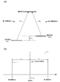
まず、本実施形態に係る光学モジュールおよび原子発振器について、図面を参照しながら説明する。本実施形態に係る原子発振器は、本実施形態に係る光学モジュールを含む。図1は、本実施形態に係る原子発振器1の機能ブロック図である。原子発振器1は、量子干渉効果を利用した発振器である。 First, an optical module and an atomic oscillator according to this embodiment will be described with reference to the drawings. The atomic oscillator according to the present embodiment includes the optical module according to the present embodiment. FIG. 1 is a functional block diagram of an atomic oscillator 1 according to this embodiment. The atomic oscillator 1 is an oscillator using a quantum interference effect.
原子発振器1は、光学モジュール2と、制御部50と、を含む。
The atomic oscillator 1 includes an
光学モジュール2は、光源10と、波長選択部20と、ガスセル30と、光検出部40と、を含む。
The
光源10は、所定の中心波長(中心周波数)を有する基本波Fと、互いに異なる波長を有する第1側帯波W1および第2側帯波W2と、を含む第1光L1を発生させる。
The
波長選択部20は、第1光L1から第1側帯波W1および第2側帯波W2を選択し、第2光L2として射出する。波長選択部20は、所定の波長範囲の光を選択して射出する光フィルター部20aと、光フィルター部20aの選択する波長範囲を変化させる光フィルター特性制御部20bと、を有する。
The
ガスセル30は、アルカリ金属ガスを封入しており、ガスセル30には、第2光L2が照射される。
The
光検出部40は、ガスセル30を透過した第2光L2の強度を検出する。
The light detection unit 40 detects the intensity of the second light L2 that has passed through the
制御部50は、光検出部40の検出結果に基づいて、第1側帯波W1および第2側帯波W2の波長(周波数)差が、ガスセル30に封入されたアルカリ金属原子の2つの基底準位のエネルギー差に相当する周波数に等しくなるように制御する。制御部50は、光検出部40の検出結果に基づいて、変調周波数fmを有する検出信号を発生させる。そして、光源10は、この検出信号に基づいて所定の周波数f0を有する基本波Fを変調して、周波数f1=f0+fmを有する第1側帯波W1、および周波数f2=f0−fmを有する第2側帯波W2を発生させる。
Based on the detection result of the light detection unit 40, the
図2(A)は、アルカリ金属原子のΛ型3準位モデルと第1側帯波W1及び第2側帯波W2の関係を示す図である。図2(B)は、光源10で発生する第1光L1の周波数スペクトラムを示す図である。
FIG. 2A is a diagram showing the relationship between the Λ-type three-level model of alkali metal atoms and the first sideband wave W1 and the second sideband wave W2. FIG. 2B is a diagram showing a frequency spectrum of the first light L1 generated by the
図2(B)に示すように、光源10において発生する第1光L1は、中心周波数f0(=v/λ0:vは光の速度、λ0はレーザー光の中心波長)を有する基本波Fと、中心周波数f0に対して上側サイドバンドに周波数f1を有する第1側帯波W1と、中心周波数f0に対して下側サイドバンドに周波数f2を有する第2側帯波W2と、を含む。第1側帯波W1の周波数f1は、f1=f0+fmであり、第2側帯波W2の周波数f2は、f2=f0−fmである。
As shown in FIG. 2B, the first light L1 generated in the
図2(A)及び図2(B)に示すように、第1側帯波W1の周波数f1と第2側帯波W2の周波数f2との周波数差が、アルカリ金属原子の基底準位GL1と基底準位GL2のエネルギー差ΔE12に相当する周波数と一致している。したがって、アルカリ金属原子は、周波数f1を有する第1側帯波W1と周波数f2を有する第2側帯波W2によってEIT現象を起こす。 As shown in FIG. 2 (A) and FIG. 2 (B), the frequency difference between the frequency f 2 of the frequency f 1 and the second sideband wave W2 of the first sideband W1 is a ground level GL1 alkali metal atom It coincides with the frequency corresponding to the energy difference Delta] E 12 ground levels GL2. Thus, alkali metal atom, causes EIT phenomenon by the second sideband wave W2 having a first sideband wave W1 and the frequency f 2 having a frequency f 1.
ここで、EIT現象について説明する。アルカリ金属原子と光との相互作用は、Λ型3準位系モデルで説明できることが知られている。図2(A)に示すように、アルカリ金属原子は2つの基底準位を有し、基底準位GL1と励起準位とのエネルギー差に相当する波長(周波数f1)を有する第1側帯波W1、あるいは基底準位GL2と励起準位とのエネルギー差に相当する波長(周波数f2)を有する第2側帯波W2を、それぞれ単独でアルカリ金属原子に照射すると、光吸収が起きる。ところが、図2(B)に示すように、このアルカリ金属原子に、周波数差f1−f2が基底準位GL1と基底準位GL2のエネルギー差ΔE12に相当する周波数と正確に一致する第1側帯波W1と第2側帯波W2を同時に照射すると、2つの基底準位の重ね合わせ状態、即ち量子干渉状態になり、励起準位への励起が停止して第1側帯波W1と第2側帯波W2がアルカリ金属原子を透過する透明化現象(EIT現象)が起きる。このEIT現象を利用し、第1側帯波W1と第2側帯波W2との周波数差f1−f2が基底準位GL1と基底準位GL2のエネルギー差ΔE12に相当する周波数からずれた時の光吸収挙動の急峻な変化を検出し制御することで、高精度な発振器をつくることができる。
Here, the EIT phenomenon will be described. It is known that the interaction between alkali metal atoms and light can be explained by a Λ-type three-level model. As shown in FIG. 2A, the alkali metal atom has two ground levels, and a first sideband having a wavelength (frequency f 1 ) corresponding to the energy difference between the ground level GL1 and the excited level. When an alkali metal atom is irradiated with W1 or a second sideband wave W2 having a wavelength (frequency f 2 ) corresponding to the energy difference between the ground level GL2 and the excitation level, light absorption occurs. However, as shown in FIG. 2B, the frequency difference f 1 -f 2 exactly matches the frequency corresponding to the energy difference ΔE 12 between the ground level GL 1 and the
しかし、図2(B)に示した第1光L1がガスセル30に直接照射されると、第1側帯波W1と第2側帯波W2と同時に、基本波Fがガスセル30すなわちアルカリ金属原子に照射されることになる。EIT現象に寄与しない基本波Fがアルカリ金属原子に照射されると、ACシュタルク効果により、アルカリ金属原子が吸収する光の波長(周波数)が変化する。これにより、アルカリ金属原子を透過する第1側帯波W1と第2側帯波W2の量が変化してしまう。EIT現象を利用した発振器においては、アルカリ金属原子を透過する第1側帯波W1と第2側帯波W2の量を検知することで変調周波数fmを安定化させ、この変調周波数fmを発信器の出力として利用することにより、発信器の周波数安定度を高めている。したがって、基本波Fによって生じるACシュタルク効果は、第1側帯波W1と第2側帯波W2の検知精度を低下させ、変調周波数fmの安定度を低下させる。すなわち、発信器の周波数安定度を低下させてしまう。
However, when the first light L1 shown in FIG. 2B is directly applied to the
図3は、波長選択部20から射出された第2光L2の周波数スペクトラムを示す図である。
Figure 3 is a diagram showing a frequency spectrum of the second light L2 emitted from the wavelength
第2光L2は、第1光L1と比べて、基本波Fが消滅または基本波Fの強度が減少した光である。図3の例では、第2光L2は、中心周波数f0に対して上側サイドバンドに周波数f1を有する第1側帯波W1、および中心周波数f0に対して下側サイドバンドに周波数f2を有する第2側帯波W2のみを有している。このように、光学モジュール2では、波長選択部20によって、基本波Fの強度を減少または基本波Fを消滅させることができる。
The second light L2 is light in which the fundamental wave F disappears or the intensity of the fundamental wave F decreases compared to the first light L1. FIG The third example, the second light L2, the center frequency the first sideband having a frequency f 1 to the upper sideband with respect to f 0 W1, and the center frequency f 2 to the lower sideband with respect to the frequency f 0 Only the second sideband W2 having Thus, in the
以下、本実施形態の原子発振器のより具体的な構成について説明する。 Hereinafter, a more specific configuration of the atomic oscillator of this embodiment will be described.
図4は、原子発振器1の構成を示すブロック図である。 FIG. 4 is a block diagram showing the configuration of the atomic oscillator 1.
原子発振器1は、図4に示すように、光学モジュール2と、電流駆動回路150と、変調回路160と、を含む。
As shown in FIG. 4, the atomic oscillator 1 includes an
光学モジュール2は、半導体レーザー110と、波長選択装置120と、ガスセル130と、光検出器140と、を含む。
The
半導体レーザー110は、所定の中心波長を有する基本波Fと、互いに異なる波長を有する第1側帯波W1および第2側帯波W2と、を含む第1光L1を発生させる。半導体レーザー110が出射するレーザー光(第1光L1)は、電流駆動回路150が出力する駆動電流によって中心周波数f0(中心波長λ0)が制御され、変調回路160の出力信号(変調信号)によって変調がかけられる。すなわち、電流駆動回路150による駆動電流に、変調信号の周波数成分を有する交流電流を重畳することにより、半導体レーザー110が出射する第1光L1に変調をかけることができる。これにより、第1光L1には、第1側帯波W1、および第2側帯波W2が生成される。半導体レーザー110において発生する光は、可干渉性を有するため、量子干渉効果を得るために好適である。
The
図2(B)に示すように、第1光L1は、中心周波数f0(=v/λ0:vは光の速度、λ0は第1光L1の中心波長)を有する基本波Fと、中心周波数f0に対して上側サイドバンドに周波数f1を有する第1側帯波W1と、中心周波数f0に対して下側サイドバンドに周波数f2を有する第2側帯波W2と、を含む。第1側帯波W1の周波数f1は、f1=f0+fmであり、第2側帯波W2の周波数f2は、f2=f0−fmである。 As shown in FIG. 2B, the first light L1 includes a fundamental wave F having a center frequency f 0 (= v / λ 0 : v is the speed of light, and λ 0 is the center wavelength of the first light L1). includes a first sideband W1 having a frequency f 1 to the upper sideband with respect to the center frequency f 0, and the second sideband wave W2 having a frequency f 2 to the lower sideband with respect to the center frequency f 0, the . Frequency f 1 of the first sideband W1 is f 1 = f 0 + f m , the frequency f 2 of the second sideband wave W2 is f 2 = f 0 -f m.
波長選択装置120は、第1光L1から第1側帯波W1および第2側帯波W2を選択し、第2光L2として射出する。波長選択装置120は、所定の波長範囲の光を選択して射出する光フィルター素子120aと、光フィルター素子120aが選択する波長範囲を変化させる光フィルター特性制御装置120bと、を有する。
The
光フィルター素子120aは、第1光から第1側帯波W1および第2側帯波W2を選択して射出することができる。そのため、光フィルター素子120aに入射した第1光L1の基本波Fの強度を減少または基本波Fを消滅させて、第2光L2として射出することができる。すなわち、第2光L2では、第1光L1と比べて、基本波Fの強度が減少または基本波Fが消滅している。図3の例では、第2光L2は、第1側帯波W1、および第2側帯波W2のみを有している。光フィルター素子120aは、後述するように、エタロンであってもよいし、ファイバーブラッググレーティング(FBG)であってもよい。
The
光フィルター特性制御装置120bは、光フィルター素子120aが選択する波長範囲(波長選択特性)を変化させることができる。光フィルター特性制御装置120bは、例えば、電気光学効果によって、光フィルター素子120a(例えば、エタロン)の波長選択特性を変化させることができる。ここで、電気光学効果とは、物質の光に対する屈折率が、外部より静電場を加えることによって変化する現象をいう。光フィルター特性制御装置120bは、例えば、光フィルター素子120aに電場を印加することにより光フィルター素子120aの屈折率を変化させ、光フィルター素子120aの波長選択特性を変化させる。波長選択装置120は、光フィルター特性制御装置120bによって、製造誤差や環境変化(熱、光など)等による光フィルター素子120aの波長選択特性のずれを補正することができるため、第1光L1から第1側帯波W1および第2側帯波W2を、精度よく選択することができる。
The optical filter
光フィルター特性制御装置120bは、光検出器140の出力信号に基づいて、光フィルター素子120aに加える電場の強度を調整し、光フィルター素子120aの波長選択特性を制御してもよい。光学モジュール2では、例えば、光フィルター素子120a、ガスセル130、光検出器140、光フィルター特性制御装置120bを通るフィードバックループにより光フィルター素子120aに印加される電場の強度が調整され、光フィルター素子120aの波長選択特性が制御される。
The optical filter
また、光フィルター特性制御装置120bは、予め取得された光フィルター素子120aの波長選択特性のずれのデータに基づいて、光フィルター素子120aに印加される電場の強度を調整し、光フィルター素子120aの波長選択特性のずれを補正してもよい。
In addition, the optical filter
ガスセル130は、容器中に気体状のアルカリ金属原子(ナトリウム(Na)原子、ルビジウム(Rb)原子、セシウム(Cs)原子等)が封入されたものである。ガスセル130には、波長選択装置120から射出された第2光L2が照射される。
The
このガスセル130に対して、アルカリ金属原子の2つの基底準位のエネルギー差に相当する周波数(波長)差を有する2つの光波(第1側帯波および第2側帯波)が照射されると、アルカリ金属原子がEIT現象を起こす。例えば、アルカリ金属原子がセシウム原子であれば、D1線における基底準位GL1と基底準位GL2のエネルギー差に相当する周波数が9.19263・・・GHzなので、周波数差が9.19263・・・GHzの2つの光波が照射されるとEIT現象を起こす。
When the
光検出器140は、ガスセル130を透過した第2光L2を検出し、検出した光の量に応じた信号強度の信号を出力する。光検出器140の出力信号は、電流駆動回路150および変調回路160に入力される。また、光検出器140の出力信号は、さらに、光フィルター特性制御装置120bに入力されてもよい。光検出器140は、例えば、フォトダイオードである。
The
電流駆動回路150は、光検出器140の出力信号に応じた大きさの駆動電流を発生させて半導体レーザー110に供給し、第1光L1の中心周波数f0(中心波長λ0)を制御する。半導体レーザー110、波長選択装置120、ガスセル130、光検出器140、電流駆動回路150を通るフィードバックループにより第1光の中心周波数f0(中心波長λ0)が微調整されて安定する。
The
変調回路160は、光検出器140の出力信号に応じた変調周波数fmを有する変調信号を発生させる。この変調信号は、光検出器140の出力信号が最大になるように変調周波数fmが微調整されながら半導体レーザー110に供給される。半導体レーザー110が出射するレーザー光は、変調信号により変調がかけられ、第1側帯波W1と第2側帯波W2を発生させる。
なお、半導体レーザー110、波長選択装置120、ガスセル130、光検出器140は、それぞれ図1の光源10、波長選択部20、ガスセル30、光検出部40に対応する。また、光フィルター素子120aは、図1の光フィルター部20aに対応し、光フィルター特性制御装置120bは、図1の光フィルター特性制御部20bに対応する。また、電流駆動回路150、変調回路160は、図1の制御部50に対応する。
The
このような構成の原子発振器1において、半導体レーザー110が発生させる第1光L1の第1側帯波W1と第2側帯波W2の周波数差がガスセル130に含まれるアルカリ金属原子の2つの基底準位のエネルギー差に相当する周波数と正確に一致しなければ、アルカリ金属原子がEIT現象を起こさないため、第1側帯波W1と照射光W2の周波数に応じて光検出器140の検出量は極めて敏感に変化する(検出量が増加する)。そのため、半導体レーザー110、波長選択装置120、ガスセル130、光検出器140、および変調回路160を通るフィードバックループにより、第1側帯波W1と第2側帯波W2との周波数差がアルカリ金属原子の2つの基底準位のエネルギー差に相当する周波数と極めて正確に一致するようにフィードバック制御がかかる。その結果、変調周波数は極めて安定した周波数になるので、変調信号を原子発振器1の出力信号(クロック出力)とすることができる。
In the atomic oscillator 1 having such a configuration, the frequency difference between the first sideband wave W1 and the second sideband wave W2 of the first light L1 generated by the
図5は、光学モジュール2の要部(半導体レーザー110および波長選択装置120)を模式的に示す断面図である。
FIG. 5 is a cross-sectional view schematically showing main parts (
光学モジュール2は、図5に示すように、さらに、基体170を含む。半導体レーザー110および波長選択装置120は、基体170に形成されている。このように半導体レーザー110および波長選択装置120がモノリシックに形成されることにより、装置の小型化を図ることができる。
As shown in FIG. 5, the
基体170の材質は、化合物半導体である。具体的には、基体170の材質は、例えば、GaAs、InP、GaN等のIII−V族半導体や、ZnO、ZnSe等のII−VI族半導体である。ここでは、基体170の材質が第1導電型(例えばn型)GaAsである場合について説明する。
The material of the
半導体レーザー110は、第1半導体層112と、活性層114と、第2半導体層116と、を含む面発光型レーザーである。
The
第1半導体層112は、基体170上に形成されている。第1半導体層112は、例えば、n型(第1導電型)Al0.9Ga0.1As層とn型Al0.15Ga0.85As層とを交互に積層した分布ブラッグ反射型(DBR)半導体ミラーである。
The
活性層114は、第1半導体層112上に形成されている。活性層114は、例えば、GaAsウェル層とAl0.3Ga0.7Asバリア層とから構成される量子井戸構造を3つ重ねた多重量子井戸(MQW)構造を有する。
The
第2半導体層116は、例えば、p型(第2導電型)Al0.15Ga0.85As層とp型Al0.9Ga0.1As層とを交互に積層したDBR半導体ミラーである。
The
p型の第2半導体層116、不純物がドーピングされていない活性層114、およびn型の第1半導体層112により、pinダイオードが形成される。
The p-type
半導体レーザー110の電極118は、基体170の下面に形成されている。電極118は、基体170を介して、第1半導体層112と電気的に接続されている。電極118は、半導体レーザー110を駆動するための一方の電極である。なお、電極118は、後述する光フィルター特性制御装置120bの第1電極128と共通の電極である。
The electrode 118 of the
半導体レーザー110の電極119は、第2半導体層116の上面に形成されている。電極119は、第2半導体層116と電気的に接続されている。電極119は、半導体レーザー110を駆動するための他方の電極である。
The
電極118,119で、pinダイオードに順方向の電圧を印加すると、活性層114において、電子と正孔との再結合が起こり、該再結合による発光が生じる。そこで生じた光が第2半導体層116と第1半導体層112との間を往復する際に誘導放出が起こり、光の強度が増幅される。光利得が光損失を上まわると、レーザー発振が起こり、第2半導体層116の上面からレーザー光(第1光L1)が出射される。半導体レーザー110から出射された光L1は、プリズム180で反射されて、波長選択装置120(光フィルター素子120a)に入射する。プリズム180は、第1光L1の進行方向を変えて、第1光L1を波長選択装置120(光フィルター素子120a)に入射させるための光学素子である。なお、本実施形態においては、第1光L1の進行方向を変えるためにプリズム180を用いているが、第1光L1を反射させて進行方向を変えることができれば、他の光学素子を用いてもよい。例えば、反射ミラーなどを用いることができる。
When a forward voltage is applied to the pin diode by the
光学モジュール2において、光フィルター素子120aは、図示の例では、エタロンである。光フィルター素子120aは、第1ミラー121と、第2ミラー122と、第1ミラー121と第2ミラー122との間に配置された基板123と、を含む。ミラー121および122は、ミラーに入射した光の一部を透過させ、一部を反射させるような半透過ミラーである。
In the
光フィルター素子120aは、ミラー121,122間の干渉作用により、入射した光L1のうち、所定の波長範囲の光(第1側帯波W1および第2側帯波W2)を透過させる。光フィルター素子120aに光が入射すると、ミラー121,122間の干渉作用により、基板123の長さ(第1ミラー121と第2ミラー122との間の距離)Dおよび基板123の屈折率に応じた波長の光が選択的に光フィルター素子120aを透過する。光フィルター素子120aでは、第1側帯波W1および第2側帯波W2に対する透過率が大きく、基本波Fに対する透過率が小さい。これにより、光フィルター素子120aに入射した光L1の基本波Fの強度を減少または基本波Fを消滅させて射出することができる。したがって、光フィルター素子120aは、例えば、第1側帯波W1および第2側帯波W2のみを含む第2光L2を射出することができる。
The
第1ミラー121と第2ミラー122は、基板123を介して、互いに対向している。第1ミラー121および第2ミラー122は、例えば、Ta2O5膜とSiO2膜とを交互に積層した多層膜からなる。ミラー121,122は、例えば、Ta2O5膜とSiO2膜を3ペア成膜した層構造を有している。第1ミラー121および第2ミラー122の反射率は、例えば、90%である。
The
基板123は、基体170上に形成されている。基板123は、基体170側から順に形成された、第1層124、第2層125、および第3層126を有している。第1層124の屈折率および第3層126の屈折率は、第2層125の屈折率より小さい。したがって、第1層124および第3層126は、クラッド層として機能し、第2層125は、第1光L1を伝播させるコア層として機能する。すなわち、基板123は、第1光L1を伝搬させる光導波路である。光学モジュール2では、基板123が光導波路であるため、光フィルター素子120aから射出される光L2のビーム径を制御することができ、ガスセル130に光L2を効率よく照射することができる。第1層124および第3層126の材質は、例えば、AlGaAsであり、第2層125の材質は、例えば、GaAsである。
The
なお、基板123は、光導波路を形成しなくてもよい。基板123は、複数の層124,125,126を有さずに、単層であってもよい。
The
基板123の材質は、特に限定されず、GaAs、InP、GaN等のIII−V族半導体や、ZnO、ZnSe等のII−VI族半導体であってもよい。基板123の材質として、例えば、GaAsを用いた場合、フリースペクトラルレンジを9.2GHz、半値全幅を0.3GHz程度とすると、基板123の長さDは28.46mm程度である。エタロンの基板の材質として一般的なSiO2を用いた場合、基板の長さは、70.66mm程度である。このように、基板123の材質として、屈折率の大きい化合物半導体を用いることで、基板123の長さDを短くすることができる。
The material of the
光フィルター特性制御装置120bは、光フィルター素子120aに電場を供給するための第1電極128および第2電極129を有している。光フィルター特性制御装置120bは、電極128,129間に電圧を印加することにより、基板123に電場を供給することができる。これにより、電気光学効果が生じて基板123の屈折率が変化し、光フィルター素子120aの波長選択特性を変化させることができる。第1電極128は、基体170の、光フィルター素子120aが位置する側と反対側に位置している。第1電極128は、基体170の下方に形成されている。第1電極128は、上述した半導体レーザー110の電極118と共通の電極である。第2電極129は、光フィルター素子120aの、基体170が位置する側と反対側に位置している。第2電極129は、絶縁層190を介して、光フィルター素子120aの上方に形成されている。電極128,129
間に、絶縁層190が形成されることにより、電極128,129間に電流が流れて電圧降下が生じることを防ぐことができる。
The optical filter
By forming the insulating
なお、ここでは、光フィルター素子120aがエタロンである場合について説明したが、光フィルター素子120aは、光ファイバーのコアに周期的な屈折率変化を与えたファイバーブラッググレーティングであってもよい。ファイバーブラッググレーティングは、光ファイバーを用いているため、変形が容易であり、設計の自由度を向上できる。
Although the case where the
また、ここでは、光フィルター素子120aの波長選択特性を、電気光学効果を用いて補正したが、例えば、熱光学効果(物質の光に対する屈折率が、外部より熱を加えることによって変化する現象をいう)を用いて補正してもよい。この場合、光学モジュール2は、光フィルター素子120aに熱を供給するための部材を有していてもよい。
Here, the wavelength selection characteristic of the
光学モジュール2および原子発振器1は、例えば、以下の特徴を有する。
The
光学モジュール2によれば、波長選択装置120が、第1光L1の基本波Fの強度を減少または基本波Fを消滅させることができる。これにより、EIT現象に寄与しない基本波Fがアルカリ金属原子に照射されることを抑制または防止できる。したがって、ACシュタルク効果による周波数変動を抑制することができ、周波数安定度の高い発振器を提供できる。
According to the
光学モジュール2によれば、波長選択装置120が、光フィルター特性制御装置120bを有しているため、製造誤差や環境変化(熱、光など)等による光フィルター素子120aの波長選択特性(光フィルター素子が選択する波長範囲)のずれを補正することができる。したがって、波長選択装置120は、第1光L1から第1側帯波W1および第2側帯波W2を、精度よく選択して射出することができる。
According to the
例えば、光フィルター素子120aがエタロンである場合、光フィルター素子120aの波長選択特性(光フィルター素子が選択する波長範囲)は、図5に示す基板123の長さDおよび基板123の屈折率に依存する。しかしながら、光フィルター素子120aの製造工程において、基板123の長さDを正確に制御することは困難であり、基板123の長さDに製造誤差が生じる場合がある。このような場合であっても、光学モジュール2によれば、光フィルター特性制御装置120bを有するため、この製造誤差に起因する波長選択特性のずれを補正することができる。
For example, when the
光学モジュール2では、光フィルター素子120aが、エタロンである。したがって、光フィルター素子を簡易な構成にすることができる。また、光フィルター素子(エタロン)120aの基板123の材質が化合物半導体である。したがって、基板123の材質が、SiO2である場合と比べて、基板123の長さDを短くすることができ、装置の小型化を図ることができる。
In the
光学モジュール2では、光フィルター特性制御装置120bが、電気光学効果によって、光フィルター素子120aの波長選択特性を変化させることができる。これにより、光フィルター素子の波長選択特性を、高精度かつ容易に制御できる。さらに、光フィルター特性制御装置120bが、基板123に電圧を印加するための第1電極128および第2電極129を含んで構成されている。したがって、光フィルター特性制御装置120bを簡易な構成にすることができる。
In the
光学モジュール2では、波長選択装置120および半導体レーザー(光源)110が基体170に形成されている。このように波長選択装置120と半導体レーザー110を基体170にモノリシックに形成することにより、装置の小型化を図ることができる。
In the
光学モジュール2では、上述のように、光フィルター素子(エタロン)120aの基板123が光導波路である。したがって、光フィルター素子120aから射出される光L2のビーム径を制御することができ、ガスセル130に効率よく光L2を照射することができる。
In the
光学モジュール2では、半導体レーザー110が面発光型レーザーである。面発光型レーザーは、端面発光型レーザーと比べて、ゲインを生じさせるための電流が少ないため、低消費電力化を図ることができる。
In the
原子発振器1では、光学モジュール2を有している。したがって、上述のように、周波数安定度の高めることができる。
The atomic oscillator 1 has an
なお、上述した実施形態は一例であって、これらに限定されるわけではない。 The above-described embodiment is an example, and the present invention is not limited to these.
例えば、上述した図5に示す半導体レーザー110は、面発光型レーザーであったが、半導体レーザーは、端面発光型レーザーであってもよい。図6は、端面発光型レーザーを用いた光学モジュール2Dの要部を模式的に示す断面図である。以下、図6に示す光学モジュール2Dにおいて、上述した図5に示す光学モジュール2の構成と同様の構成については同一の符号を付し、その説明を省略する。
For example, although the
第1半導体層112は、基体170上に形成されている。第1半導体層112としては、例えば、第1導電型(例えばn型)AlGaAs層などを用いることができる。
The
活性層114は、第1半導体層112上に形成されている。活性層114は、例えば、GaAsウェル層とAlGaAsバリア層とから構成される量子井戸構造を3つ重ねた多重量子井戸(MQW)構造を有する。
The
第2半導体層116は、活性層114上に形成されている。第2半導体層116としては、例えば、第2導電型(例えばp型)のAlGaAs層などを用いることができる。
The
例えば、p型の第2半導体層116、不純物がドーピングされていない活性層114、およびn型の第1半導体層112により、pinダイオードが構成される。第2半導体層116および第1半導体層112の各々は、活性層114よりも禁制帯幅が大きく、屈折率が小さい層である。活性層114は、光を増幅する機能を有する。第1半導体層112および第2半導体層116は、活性層114を挟んで、注入キャリア(電子および正孔)並びに光を閉じ込める機能を有する。
For example, the p-type
半導体レーザー110では、電極118,119間に、pinダイオードの順バイアス電圧を印加すると、活性層114において電子と正孔との再結合が起こる。この再結合により発光が生じる。この生じた光を起点として、連鎖的に誘導放出が起こり、光強度が増幅される。光利得が光損失を上まわると、レーザー発振が起こり、レーザー光が生じ、活性層114の側面からレーザー光(第1光L1)が出射される。
In the
光学モジュール2Dによれば、半導体レーザー110として端面発光型レーザーを用いることで、半導体レーザー110の各層112,114,116の積層方向に対して垂直にレーザー光を出射することができる。したがって、各層112,114,116の膜厚の制御によって、半導体レーザー110と波長選択装置120との間のアライメントができる。したがって、半導体レーザー110と波長選択装置120との間のアライメント精度を向上させることができる。さらに、例えば、波長選択装置120にレーザー光を入射させるためのプリズム等の光学素子が不要となる。
According to the
上記のように、本発明の実施形態について詳細に説明したが、本発明の新規事項および効果から実体的に逸脱しない多くの変形が可能であることは当業者には容易に理解できよう。従って、このような変形例はすべて本発明の範囲に含まれるものとする。 Although the embodiments of the present invention have been described in detail as described above, those skilled in the art will readily understand that many modifications are possible without substantially departing from the novel matters and effects of the present invention. Accordingly, all such modifications are intended to be included in the scope of the present invention.
1 原子発振器、2 光学モジュール、10 光源、20 波長選択部、
20a 光フィルター部、20b 光フィルター特性制御部、
30 ガスセル、40 光検出部、50 制御部、110 半導体レーザー、
112 第1半導体層、114 活性層、116 第2半導体層、
118,119 電極、120 波長選択装置、120a 光フィルター素子、
120b 光フィルター特性制御装置、121 第1ミラー、122 第2ミラー、
123 基板、124 第1層、125 第2層、126 第3層、
128 第1電極、129 第2電極、130 ガスセル、
140 光検出器、150 電流駆動回路、160 変調回路、170 基体、
180 プリズム
1 atomic oscillator, 2 optical module, 10 light source, 20 wavelength selector,
20a optical filter unit, 20b optical filter characteristic control unit,
30 gas cell, 40 light detector, 50 controller, 110 semiconductor laser,
112 first semiconductor layer, 114 active layer, 116 second semiconductor layer,
118,119 electrodes, 120 wavelength selection device, 120a optical filter element,
120b optical filter characteristic control device, 121 first mirror, 122 second mirror,
123 substrate, 124 first layer, 125 second layer, 126 third layer,
128 first electrode, 129 second electrode, 130 gas cell,
140 photodetector, 150 current drive circuit, 160 modulation circuit, 170 substrate,
180 prism
Claims (8)
所定の波長を有する基本波、当該基本波の側帯波、を含む光を出射する面発光型レーザーと、
前記面発光型レーザーから出射された光が入射する入射部を有し、当該入射部に入射した光のうち前記側帯波を透過させる波長選択部と、
アルカリ金属ガスを封入し、前記波長選択部を透過した光が照射されるガスセルと、
前記ガスセルに照射された光のうち前記ガスセルを透過した光の強度を検出する光検出部と、
化合物半導体の基体と、
を含み、
前記波長選択部は、
所定の波長範囲の光を透過させる光フィルター部と、
前記光フィルター部が透過させる光の波長範囲を変化させる光フィルター特性制御部と、
を有し、
前記面発光型レーザーは、前記基体上に位置し、かつ、光を出射する出射部を備え、
前記基体は、前記面発光型レーザーが前記基体上に位置する面に対して突出する凸部を含み、
前記光フィルター部は、前記凸部上に位置し、
前記面発光型レーザーから出射された光は、反射面を有するプリズムを介して前記光フィルター部に入射し、
前記入射部と前記基体の前記面発光型レーザーが位置する面との距離は、前記出射部と前記基体の前記面発光型レーザーが位置する面との距離より離れていることを特徴とする原子発振器用の光学モジュール。 An optical module for an atomic oscillator using the quantum interference effect,
A surface emitting laser that emits light including a fundamental wave having a predetermined wavelength, and a sideband of the fundamental wave;
A wavelength selection unit that includes an incident unit on which light emitted from the surface-emitting laser is incident, and transmits the sideband among the light incident on the incident unit;
A gas cell in which an alkali metal gas is sealed and irradiated with light transmitted through the wavelength selection unit;
A light detector for detecting the intensity of light transmitted through the gas cell among the light irradiated to the gas cell;
A compound semiconductor substrate;
Including
The wavelength selector is
An optical filter that transmits light in a predetermined wavelength range;
An optical filter characteristic control unit that changes a wavelength range of light transmitted by the optical filter unit;
Have
The surface-emitting type laser is located on the substrate and includes an emission part that emits light,
The base includes a convex portion that protrudes with respect to a surface on which the surface-emitting laser is positioned on the base;
The optical filter portion is located on the convex portion,
The light emitted from the surface emitting laser is incident on the optical filter unit through a prism having a reflective surface,
The distance between the incident portion and the surface of the substrate on which the surface-emitting laser is located is greater than the distance between the emitting portion and the surface of the substrate on which the surface-emitting laser is located. Optical module for oscillator.
前記光フィルター特性制御部は、電気光学効果によって、前記光フィルター部が透過させる光の波長範囲を変化させる、ことを特徴とする請求項1に記載の原子発振器用の光学
モジュール。 The optical filter portion is an etalon,
The optical module for an atomic oscillator according to claim 1, wherein the optical filter characteristic control unit changes a wavelength range of light transmitted by the optical filter unit by an electro-optic effect.
前記波長選択部に入射した光を反射させ、互いに対向する第1ミラーおよび第2ミラーと、
前記第1ミラーと前記第2ミラーとの間に配置された基板と、
を有し、
前記基板の材質は、化合物半導体である、ことを特徴とする請求項2に記載の原子発振器用の光学モジュール。 The optical filter section is
A first mirror and a second mirror that reflect the light incident on the wavelength selection unit and face each other;
A substrate disposed between the first mirror and the second mirror;
Have
The optical module for an atomic oscillator according to claim 2, wherein a material of the substrate is a compound semiconductor.
前記第2電極は、前記光フィルター部の前記基体が位置する側と反対側に位置する、ことを特徴とする請求項4に記載の原子発振器用の光学モジュール。 The first electrode is located on the opposite side of the base on which the optical filter portion is located,
5. The optical module for an atomic oscillator according to claim 4, wherein the second electrode is located on a side opposite to a side where the base of the optical filter portion is located.
前記第1層の屈折率および前記第3層の屈折率は、前記第2層の屈折率より小さく、
前記第2層は、前記面発光型レーザーから出射した光を伝播させる、ことを特徴とする請求項5に記載の原子発振器用の光学モジュール。 The substrate of the optical filter portion has a first layer, a second layer, and a third layer laminated from the base side,
The refractive index of the first layer and the refractive index of the third layer are smaller than the refractive index of the second layer,
The optical module for an atomic oscillator according to claim 5, wherein the second layer propagates light emitted from the surface-emitting type laser.
所定の波長を有する基本波、当該基本波の側帯波、を含む光を出射する面発光型レーザーと、
前記面発光型レーザーから出射された光が入射する入射部を有し、当該入射部に入射した光のうち前記側帯波を透過させる波長選択部と、
アルカリ金属ガスを封入し、前記波長選択部を透過した光が照射されるガスセルと、
前記ガスセルに照射された光のうち前記ガスセルを透過した光の強度を検出する光検出部と、
化合物半導体の基体と、
を含み、
前記波長選択部は、
所定の波長範囲の光を透過させる光フィルター部と、
前記光フィルター部が透過させる光の波長範囲を変化させる光フィルター特性制御部と、
を有し、
前記面発光型レーザーは、前記基体上に位置し、かつ、光を出射する出射部を備え、
前記基体は、前記面発光型レーザーが前記基体上に位置する面に対して突出する凸部を含み、
前記光フィルター部は、前記凸部上に位置し、
前記面発光型レーザーから出射された光は、反射面を有するプリズムを介して前記光フィルター部に入射し、
前記入射部と前記基体の前記面発光型レーザーが位置する面との距離は、前記出射部と前記基体の前記面発光型レーザーが位置する面との距離より離れていることを特徴とする原子発振器。 An atomic oscillator that uses the quantum interference effect,
A surface emitting laser that emits light including a fundamental wave having a predetermined wavelength, and a sideband of the fundamental wave;
A wavelength selection unit that includes an incident unit on which light emitted from the surface-emitting laser is incident, and transmits the sideband among the light incident on the incident unit ;
A gas cell in which an alkali metal gas is sealed and irradiated with light transmitted through the wavelength selection unit;
A light detector for detecting the intensity of light transmitted through the gas cell among the light irradiated to the gas cell;
A compound semiconductor substrate;
Including
The wavelength selector is
An optical filter that transmits light in a predetermined wavelength range;
An optical filter characteristic control unit that changes a wavelength range of light transmitted by the optical filter unit;
Have
The surface-emitting type laser is located on the substrate and includes an emission part that emits light,
The base includes a convex portion that protrudes with respect to a surface on which the surface-emitting laser is positioned on the base;
The optical filter portion is located on the convex portion,
The light emitted from the surface emitting laser is incident on the optical filter unit through a prism having a reflective surface,
The distance between the incident portion and the surface of the substrate on which the surface-emitting laser is located is greater than the distance between the emitting portion and the surface of the substrate on which the surface-emitting laser is located. Oscillator.
Priority Applications (4)
| Application Number | Priority Date | Filing Date | Title |
|---|---|---|---|
| JP2011055432A JP5910806B2 (en) | 2011-03-14 | 2011-03-14 | Optical module and atomic oscillator for an atomic oscillator |
| CN201210064106.9A CN102684694B (en) | 2011-03-14 | 2012-03-12 | Optical module for atomic oscillator and atomic oscillator |
| EP12159014.5A EP2501044B1 (en) | 2011-03-14 | 2012-03-12 | Optical module for atomic oscillator and atomic oscillator |
| US13/418,688 US8638177B2 (en) | 2011-03-14 | 2012-03-13 | Optical module for atomic oscillator and atomic oscillator |
Applications Claiming Priority (1)
| Application Number | Priority Date | Filing Date | Title |
|---|---|---|---|
| JP2011055432A JP5910806B2 (en) | 2011-03-14 | 2011-03-14 | Optical module and atomic oscillator for an atomic oscillator |
Publications (3)
| Publication Number | Publication Date |
|---|---|
| JP2012191119A JP2012191119A (en) | 2012-10-04 |
| JP2012191119A5 JP2012191119A5 (en) | 2014-04-10 |
| JP5910806B2 true JP5910806B2 (en) | 2016-04-27 |
Family
ID=45977171
Family Applications (1)
| Application Number | Title | Priority Date | Filing Date |
|---|---|---|---|
| JP2011055432A Active JP5910806B2 (en) | 2011-03-14 | 2011-03-14 | Optical module and atomic oscillator for an atomic oscillator |
Country Status (4)
| Country | Link |
|---|---|
| US (1) | US8638177B2 (en) |
| EP (1) | EP2501044B1 (en) |
| JP (1) | JP5910806B2 (en) |
| CN (1) | CN102684694B (en) |
Families Citing this family (13)
| Publication number | Priority date | Publication date | Assignee | Title |
|---|---|---|---|---|
| JP6056118B2 (en) * | 2011-03-23 | 2017-01-11 | セイコーエプソン株式会社 | Optical module and atomic oscillator |
| JP6028922B2 (en) * | 2013-02-15 | 2016-11-24 | セイコーエプソン株式会社 | Quantum interference device and atomic oscillator |
| CN103454902B (en) * | 2013-06-24 | 2015-12-09 | 苏州大学 | A kind of atomic clock |
| JP6234090B2 (en) * | 2013-07-09 | 2017-11-22 | 三菱電機株式会社 | Semiconductor device |
| US9442293B2 (en) | 2014-05-06 | 2016-09-13 | Microsoft Technology Licensing, Llc | Composite variable light attenuator |
| US9746739B2 (en) | 2014-06-05 | 2017-08-29 | Microsoft Technology Licensing, Llc | See-through dimming panel |
| US20160363617A1 (en) | 2015-06-15 | 2016-12-15 | The Regents Of The University Of Michigan | Atom-Based Electromagnetic Radiation Electric-Field Sensor |
| CN107579409B (en) * | 2017-09-22 | 2019-06-18 | 合肥工业大学 | A kind of bright squeezed type light field generator |
| KR20230044321A (en) | 2017-12-18 | 2023-04-03 | 리드베르크 테크놀로지스 인코퍼레이티드 | Atom-based electromagnetic field sensing element and measurement system |
| US10656405B2 (en) * | 2018-01-20 | 2020-05-19 | International Business Machines Corporation | Color image capture under controlled environment for mobile devices |
| CN110333651B (en) * | 2019-07-15 | 2021-04-02 | 温州激光与光电子协同创新中心 | Laser atomic clock locked based on coherent population trapping mode |
| CN110361604B (en) * | 2019-07-23 | 2021-08-13 | 北京无线电计量测试研究所 | Electric field detection quantum component, preparation method and quantum field intensity sensor |
| CN117269935B (en) * | 2023-11-21 | 2024-03-29 | 中国科学技术大学 | Full-receiving light path of small-caliber monoatomic filter of resonance fluorescence laser radar |
Family Cites Families (17)
| Publication number | Priority date | Publication date | Assignee | Title |
|---|---|---|---|---|
| US6201821B1 (en) | 2000-06-05 | 2001-03-13 | Agilent Technologies, Inc. | Coherent population trapping-based frequency standard having a reduced magnitude of total a.c. stark shift |
| US6806784B2 (en) * | 2001-07-09 | 2004-10-19 | The National Institute Of Standards And Technology | Miniature frequency standard based on all-optical excitation and a micro-machined containment vessel |
| US6570459B1 (en) | 2001-10-29 | 2003-05-27 | Northrop Grumman Corporation | Physics package apparatus for an atomic clock |
| DE60329666D1 (en) * | 2002-04-09 | 2009-11-26 | California Inst Of Techn | ATOM WATCH BASED ON AN OPTOELECTRONIC OSCILLATOR |
| US6900702B2 (en) | 2002-08-14 | 2005-05-31 | Honeywell International Inc. | MEMS frequency standard for devices such as atomic clock |
| WO2004111717A1 (en) * | 2003-06-13 | 2004-12-23 | Nippon Telegraph And Telephone Corporation | Variable wavelength optical filter |
| US6993058B2 (en) * | 2003-04-28 | 2006-01-31 | Agilent Technologies, Inc. | Coherent population trapping detector |
| CN2664290Y (en) * | 2003-06-24 | 2004-12-15 | 深圳市东方汉华软件技术有限公司 | A circuit structure for temperature-compensation and frequency correction of oscillation frequency source |
| JP2005037762A (en) * | 2003-07-17 | 2005-02-10 | Sun Tec Kk | Optical element, tunable optical filter, optical add drop module, and tunable light source |
| JP4720635B2 (en) | 2006-06-14 | 2011-07-13 | エプソントヨコム株式会社 | Atomic oscillator, passive atomic oscillator, temperature control method for atomic oscillator, and temperature control method for passive atomic oscillator |
| JP2009089116A (en) | 2007-10-01 | 2009-04-23 | Epson Toyocom Corp | Optical module for atomic oscillator |
| JP5343356B2 (en) | 2008-01-07 | 2013-11-13 | セイコーエプソン株式会社 | Atomic oscillator |
| JP4952603B2 (en) | 2008-02-05 | 2012-06-13 | セイコーエプソン株式会社 | Atomic oscillator |
| US7944317B2 (en) * | 2008-08-11 | 2011-05-17 | Honeywell International Inc. | Cold atom micro primary standard |
| JP5001239B2 (en) * | 2008-08-19 | 2012-08-15 | 日本電信電話株式会社 | Semiconductor tunable laser |
| JP5256999B2 (en) * | 2008-10-29 | 2013-08-07 | セイコーエプソン株式会社 | Physical part of atomic oscillator |
| JP5429469B2 (en) * | 2009-09-07 | 2014-02-26 | セイコーエプソン株式会社 | Quantum interference device, atomic oscillator and magnetic sensor |
-
2011
- 2011-03-14 JP JP2011055432A patent/JP5910806B2/en active Active
-
2012
- 2012-03-12 EP EP12159014.5A patent/EP2501044B1/en not_active Not-in-force
- 2012-03-12 CN CN201210064106.9A patent/CN102684694B/en active Active
- 2012-03-13 US US13/418,688 patent/US8638177B2/en active Active
Also Published As
| Publication number | Publication date |
|---|---|
| US8638177B2 (en) | 2014-01-28 |
| EP2501044B1 (en) | 2014-02-26 |
| US20120235756A1 (en) | 2012-09-20 |
| JP2012191119A (en) | 2012-10-04 |
| CN102684694A (en) | 2012-09-19 |
| EP2501044A1 (en) | 2012-09-19 |
| CN102684694B (en) | 2017-04-12 |
Similar Documents
| Publication | Publication Date | Title |
|---|---|---|
| JP5910806B2 (en) | Optical module and atomic oscillator for an atomic oscillator | |
| JP5699467B2 (en) | Optical module and atomic oscillator | |
| JP5910808B2 (en) | Optical module and atomic oscillator for an atomic oscillator | |
| JP5910807B2 (en) | Optical module and atomic oscillator for an atomic oscillator | |
| JP2006261424A (en) | Semiconductor laser device and gas detector | |
| CN104937791A (en) | Laser device, optical modulation device, and optical semiconductor element | |
| JP6056118B2 (en) | Optical module and atomic oscillator | |
| JP2015175902A (en) | Optical waveguide, spot size converter, polarization filter, optical coupler, optical detector, optical splitter, and laser element | |
| JP2019062036A (en) | Modulation light source | |
| JP5700056B2 (en) | Optical module and atomic oscillator | |
| JP2005345949A (en) | Wavelength conversion light source and driving method therefor | |
| JP2015128172A (en) | Optical module and atomic oscillator | |
| JP2010102045A (en) | Mode synchronization semiconductor laser | |
| US20130044773A1 (en) | Optical sources having proximity coupled laser source and waveguide | |
| JP2016072371A (en) | Atom oscillator | |
| JP2013229357A (en) | Distribution feedback type semiconductor laser and otdr device |
Legal Events
| Date | Code | Title | Description |
|---|---|---|---|
| A521 | Request for written amendment filed |
Free format text: JAPANESE INTERMEDIATE CODE: A523 Effective date: 20140226 |
|
| A621 | Written request for application examination |
Free format text: JAPANESE INTERMEDIATE CODE: A621 Effective date: 20140226 |
|
| RD07 | Notification of extinguishment of power of attorney |
Free format text: JAPANESE INTERMEDIATE CODE: A7427 Effective date: 20140619 |
|
| A131 | Notification of reasons for refusal |
Free format text: JAPANESE INTERMEDIATE CODE: A131 Effective date: 20150204 |
|
| A521 | Request for written amendment filed |
Free format text: JAPANESE INTERMEDIATE CODE: A523 Effective date: 20150327 |
|
| A131 | Notification of reasons for refusal |
Free format text: JAPANESE INTERMEDIATE CODE: A131 Effective date: 20150902 |
|
| A521 | Request for written amendment filed |
Free format text: JAPANESE INTERMEDIATE CODE: A523 Effective date: 20151029 |
|
| TRDD | Decision of grant or rejection written | ||
| A01 | Written decision to grant a patent or to grant a registration (utility model) |
Free format text: JAPANESE INTERMEDIATE CODE: A01 Effective date: 20160302 |
|
| A61 | First payment of annual fees (during grant procedure) |
Free format text: JAPANESE INTERMEDIATE CODE: A61 Effective date: 20160315 |
|
| R150 | Certificate of patent or registration of utility model |
Ref document number: 5910806 Country of ref document: JP Free format text: JAPANESE INTERMEDIATE CODE: R150 |
|
| R250 | Receipt of annual fees |
Free format text: JAPANESE INTERMEDIATE CODE: R250 |
|
| R250 | Receipt of annual fees |
Free format text: JAPANESE INTERMEDIATE CODE: R250 |