JP5907479B2 - ANTENNA DEVICE AND ELECTRONIC DEVICE - Google Patents
ANTENNA DEVICE AND ELECTRONIC DEVICE Download PDFInfo
- Publication number
- JP5907479B2 JP5907479B2 JP2013059429A JP2013059429A JP5907479B2 JP 5907479 B2 JP5907479 B2 JP 5907479B2 JP 2013059429 A JP2013059429 A JP 2013059429A JP 2013059429 A JP2013059429 A JP 2013059429A JP 5907479 B2 JP5907479 B2 JP 5907479B2
- Authority
- JP
- Japan
- Prior art keywords
- conductive
- antenna
- conductive element
- housing
- antenna element
- Prior art date
- Legal status (The legal status is an assumption and is not a legal conclusion. Google has not performed a legal analysis and makes no representation as to the accuracy of the status listed.)
- Active
Links
Images


Classifications
-
- H—ELECTRICITY
- H01—ELECTRIC ELEMENTS
- H01Q—ANTENNAS, i.e. RADIO AERIALS
- H01Q1/00—Details of, or arrangements associated with, antennas
- H01Q1/27—Adaptation for use in or on movable bodies
- H01Q1/273—Adaptation for carrying or wearing by persons or animals
-
- H—ELECTRICITY
- H01—ELECTRIC ELEMENTS
- H01Q—ANTENNAS, i.e. RADIO AERIALS
- H01Q1/00—Details of, or arrangements associated with, antennas
- H01Q1/12—Supports; Mounting means
- H01Q1/22—Supports; Mounting means by structural association with other equipment or articles
- H01Q1/24—Supports; Mounting means by structural association with other equipment or articles with receiving set
- H01Q1/241—Supports; Mounting means by structural association with other equipment or articles with receiving set used in mobile communications, e.g. GSM
- H01Q1/242—Supports; Mounting means by structural association with other equipment or articles with receiving set used in mobile communications, e.g. GSM specially adapted for hand-held use
- H01Q1/243—Supports; Mounting means by structural association with other equipment or articles with receiving set used in mobile communications, e.g. GSM specially adapted for hand-held use with built-in antennas
-
- H—ELECTRICITY
- H01—ELECTRIC ELEMENTS
- H01Q—ANTENNAS, i.e. RADIO AERIALS
- H01Q5/00—Arrangements for simultaneous operation of antennas on two or more different wavebands, e.g. dual-band or multi-band arrangements
- H01Q5/30—Arrangements for providing operation on different wavebands
- H01Q5/378—Combination of fed elements with parasitic elements
- H01Q5/385—Two or more parasitic elements
-
- H—ELECTRICITY
- H01—ELECTRIC ELEMENTS
- H01Q—ANTENNAS, i.e. RADIO AERIALS
- H01Q1/00—Details of, or arrangements associated with, antennas
- H01Q1/12—Supports; Mounting means
- H01Q1/22—Supports; Mounting means by structural association with other equipment or articles
- H01Q1/2283—Supports; Mounting means by structural association with other equipment or articles mounted in or on the surface of a semiconductor substrate as a chip-type antenna or integrated with other components into an IC package
Description
本発明は、アンテナ装置及び電子機器に関し、特に、小型の筐体を有し、かつ、無線通信機能を備えた携帯型の電子機器に適用されるアンテナ装置に関する。 The present invention relates to an antenna device and an electronic device, and more particularly to an antenna device applied to a portable electronic device having a small casing and having a wireless communication function.
近年、各種の無線通信機能を備えた携帯型の電子機器の普及が著しい。例えばスマートフォン(高機能携帯電話機)やタブレット型端末、デジタルカメラ、スポーツウォッチ(ランニングウォッチ)、登山用GPS機器等の種々の電子機器において、公衆の無線通信回線(携帯電話回線、高速データ通信回線等)への接続機能や、無線LAN(Local Area Network)やブルートゥース(Bluetooth;登録商標)等の近距離無線通信機能、GPS(Global Positioning System;全地球測位システム)衛星からの電磁波を利用した測位機能を搭載したものが知られている。 In recent years, portable electronic devices having various wireless communication functions have been widely used. For example, in various electronic devices such as smart phones (high-function mobile phones), tablet-type terminals, digital cameras, sports watches (running watches), and climbing GPS devices, public wireless communication lines (mobile phone lines, high-speed data communication lines, etc.) ), Short-range wireless communication functions such as wireless local area network (LAN) and Bluetooth (registered trademark), and positioning functions using electromagnetic waves from GPS (Global Positioning System) satellites The one with is known.
特に、近年の健康志向の高まりや趣味の多様化等により、日常的にウォーキングやランニング、サイクリング等の運動を行って健康状態を維持、増進する人々や、登山やトレッキング等により自然の中で過ごす趣味を持つ人々が増えている。このような場面で利用されるスポーツウォッチやアウトドア用の電子機器においては、小型軽量であることに加え、例えば無線LANやブルートゥース(登録商標)等の近距離無線通信機能や、GPSによる測位機能、時刻修正機能を備えた高機能な機器であることが求められている。現在、このような要望に対応する機器が種々商品化されている。このような電子機器については、例えば特許文献1に、GPS衛星からの電磁波を受信するための方形状のパッチアンテナが、筐体内の略中央に配置された構造を有する腕時計型端末が記載されている。
In particular, people who maintain and improve their health by performing daily activities such as walking, running, cycling, etc. due to the recent increase in health consciousness and diversification of hobbies, and spending in nature by climbing, trekking, etc. An increasing number of people have hobbies. In sports watches and outdoor electronic devices used in such situations, in addition to being small and light, for example, short-range wireless communication functions such as wireless LAN and Bluetooth (registered trademark), GPS positioning functions, It is required to be a highly functional device with a time correction function. Currently, various devices that meet such demands have been commercialized. For such an electronic device, for example,
上述した特許文献1に記載されているような腕時計型端末においては、小型筐体に多くの電子部品を内蔵する必要があるため、GPSや各種の無線通信のためのアンテナとして、小型のものを適用せざるを得ないという制約がある。そのため、電磁波の送受信特性の劣化や、電磁波の狭帯域化等の無線通信機能の性能劣化を招くという問題を有していた。
In the wristwatch type terminal described in
また、特許文献1に示したような方形型のパッチアンテナ等を適用した場合、良好な送受信特性を実現するためには、アンテナのサイズ(面積と厚み)を考慮する必要がある。ここで、アンテナの性能を高めるためにアンテナを大型化した場合には、周辺の電子部品のレイアウト設計や、腕時計型端末(電子機器)の筐体のデザインに影響を与える可能性があり、一方、筐体を小型化、薄型化しようとすると、アンテナの構造設計やアンテナの性能に制約が生じることがあるという問題も有していた。
In addition, when a rectangular patch antenna or the like as shown in
そこで、本発明の目的は、上述した問題点に鑑み、各種の無線通信やGPS等に適用されるアンテナ装置の実装スペースを狭小化することができて、設計上の制約を抑制しつつ電磁波の送受信特性に優れたアンテナ装置、及び、当該アンテナ装置を備えた電子機器を提供することを目的とする。 Therefore, in view of the above-described problems, the object of the present invention is to reduce the mounting space of an antenna device applied to various types of wireless communication, GPS, etc. It is an object of the present invention to provide an antenna device having excellent transmission / reception characteristics and an electronic device including the antenna device.
本発明に係る第1のアンテナ装置は、
少なくとも一つの特定の周波数の電磁波を送信又は受信するアンテナ素子と、
前記アンテナ素子と離間して前記アンテナ素子に対向して配置され、導電性を有する材料により形成され、無給電素子をなす導電性素子と、
内部に密閉された空間を有する筐体と、
を備え、
前記アンテナ素子は、前記筐体の内部に設けられており、
前記導電性素子は、
前記筐体に取り付けられたバンド部材内に設けられ、
前記アンテナ素子と電磁界結合して、前記特定の周波数に対して共振して、前記電磁波を送信又は受信し、
前記バンド部材の、前記導電性素子に接している領域の部材は、絶縁性を有する部材により形成され、
前記導電性素子は、
直線状の第1の辺と直線状の第2の辺とを有し、
前記第1の辺及び前記第2の辺は、それぞれ前記特定の周波数の波長の1/2 n (n=0、1、2、3、・・)の長さを有し、
前記導電性素子は、前記第1の辺と前記第2の辺とが互いに交差する方向に延在して、屈曲した形状を有していることを特徴とする。
本発明に係る第2のアンテナ装置は、
少なくとも一つの特定の周波数の電磁波を送信又は受信するアンテナ素子と、
前記アンテナ素子と離間して前記アンテナ素子に対向して配置され、導電性を有する材料により形成され、無給電素子をなす導電性素子と、
内部に密閉された空間を有する筐体と、
を備え、
前記アンテナ素子は、前記筐体の内部に設けられており、
前記導電性素子は、
前記筐体の外面又は前記筐体を構成する部材内の、前記アンテナ素子に対向する位置に設けられ、
前記アンテナ素子と電磁界結合して、前記特定の周波数に対して共振して、前記電磁波を送信又は受信し、
前記筐体の、前記導電性素子に接している領域の部材は、絶縁性を有する材料により形成され、
前記導電性素子は、直線状の第1の辺を有し、
前記第1の辺の長さは前記特定の周波数の波長の1/2 n (n=0、1、2、3、・・)の長さに設定されていることを特徴とする。
A first antenna device according to the present invention includes:
An antenna element for transmitting or receiving electromagnetic waves of at least one specific frequency;
A conductive element disposed away from the antenna element and facing the antenna element, formed of a conductive material, and forming a parasitic element;
A housing having a sealed space inside,
With
The antenna element is provided inside the housing,
The conductive element is
Provided in-band member attached to the housing,
Said antenna elements and electromagnetically coupling said resonating to a particular frequency, transmitting or receiving the electromagnetic wave,
A member of the band member that is in contact with the conductive element is formed of an insulating member,
The conductive element is
A linear first side and a linear second side;
Each of the first side and the second side has a length of 1/2 n (n = 0, 1, 2, 3,...) Of the wavelength of the specific frequency ,
The conductive elements may extend in a direction of the first side and said second side intersect with each other, it characterized that you have have a bent shape.
The second antenna device according to the present invention is:
An antenna element for transmitting or receiving electromagnetic waves of at least one specific frequency;
A conductive element disposed away from the antenna element and facing the antenna element, formed of a conductive material, and forming a parasitic element;
A housing having a sealed space inside,
With
The antenna element is provided inside the housing,
The conductive element is
Provided at a position facing the antenna element in the outer surface of the casing or a member constituting the casing,
Electromagnetic field coupling with the antenna element, resonating with respect to the specific frequency, transmitting or receiving the electromagnetic wave,
The member of the region in contact with the conductive element of the housing is formed of an insulating material,
The conductive element has a linear first side;
The length of the first side is set to a length of 1/2 n (n = 0, 1, 2, 3,...) Of the wavelength of the specific frequency .
本発明に係る電子機器は、
外部の機器との通信を制御する通信制御機能を有する電子機器本体部と、
上記のアンテナ装置と、
を備え、
前記アンテナ装置に前記電子機器本体部から信号が供給されていることを特徴とする。
The electronic device according to the present invention is
An electronic device main body having a communication control function for controlling communication with an external device ;
The above antenna device;
With
A signal is supplied to the antenna device from the electronic device main body.
本発明によれば、各種の無線通信やGPS等に適用されるアンテナ装置の実装スペースを狭小化することができて設計上の制約を抑制するとともに、優れた電磁波の放射特性を実現することができる。 According to the present invention, it is possible to reduce the mounting space of an antenna device applied to various types of wireless communication, GPS, and the like, thereby suppressing design restrictions and realizing excellent electromagnetic wave radiation characteristics. it can.
以下、本発明に係るアンテナ装置及び電子機器について、実施形態を示して詳しく説明する。
<第1の実施形態>
Hereinafter, an antenna device and an electronic apparatus according to the present invention will be described in detail with reference to embodiments.
<First Embodiment>
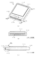
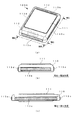
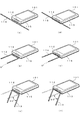
図1は、本発明に係るアンテナ装置を適用した電子機器の第1の実施形態を示す概略構成図である。ここで、図1(a)は、本実施形態に係る電子機器の外観構成を示す斜視図であり、図1(b)は、図1(a)に示した電子機器におけるIB−IB線(本明細書においては図1中に示したローマ数字の「1」に対応する記号として便宜的に「I」を用いる。以下同じ。)に沿って矢視した側面を示す図であり、図1(c)は、図1(a)に示した電子機器におけるIC−IC線に沿って矢視した側面を示す図である。なお、図1においては、図示を明瞭にするために、導電性素子に便宜的にハッチングを施して示した。また、図2は、本実施形態に係る電子機器の要部の拡大断面図である。ここで、図2(a)は、図1(c)に示したIIA部(本明細書においては図1中に示したローマ数字の「2」に対応する記号として便宜的に「II」を用いる)の拡大断面図であり、図2(b)、(c)は、当該IIA部の他の構成例を示す図である。 FIG. 1 is a schematic configuration diagram showing a first embodiment of an electronic apparatus to which an antenna device according to the present invention is applied. Here, FIG. 1A is a perspective view showing an external configuration of the electronic apparatus according to the present embodiment, and FIG. 1B is an IB-IB line in the electronic apparatus shown in FIG. In this specification, “I” is used as a symbol corresponding to the Roman numeral “1” shown in FIG. 1 for the sake of convenience. The same shall apply hereinafter.) FIG. (C) is a figure which shows the side surface seen from the arrow along the IC-IC line in the electronic device shown to Fig.1 (a). In FIG. 1, for the sake of clarity, the conductive elements are shown hatched for convenience. FIG. 2 is an enlarged cross-sectional view of a main part of the electronic apparatus according to the present embodiment. Here, FIG. 2A shows the IIA section shown in FIG. 1C (in this specification, “II” is used as a symbol corresponding to the Roman numeral “2” shown in FIG. 1 for convenience). FIG. 2B and FIG. 2C are diagrams showing another configuration example of the IIA part.
第1の実施形態に係る電子機器100Aは、例えば図1(a)〜(c)に示すように、矩形状の平面形状を有する一対の面(図面上面及び下面)が対向して配置された筐体110を有している。筐体110の一面側(図面上面側)には、例えば表示部111が組み込まれ、電子機器100Aの動作や機能に応じた種々の情報が表示される。また、筐体110の内部には、アンテナ素子112が設けられている。アンテナ素子112は、例えば図2(a)に示すように、絶縁性の回路基板114上に、通信回路(図示を省略)とともに搭載された構成を有している。上記のアンテナ素子112に対向する筐体110の一側面(図1(a)手前側の側面)の外面には、当該側面の延在方向(図1(b)の左右方向)に沿って、導電性素子113が設けられている。ここで、本発明に係るアンテナ装置は、少なくとも上記のアンテナ素子112と導電性素子113とを含む構成に対応している。
In the
電子機器100Aの筐体110は、少なくとも筐体110の内部に設けられたアンテナ素子112と対向し、かつ、導電性素子113が設けられている領域及びその近傍(具体的には、図2(a)に示す導電性素子113が設けられる領域の側面部分及びその近傍)が、樹脂材料等の絶縁性部材により形成されている。
The
アンテナ素子112及び回路基板114を含む通信回路は、例えば無線LANやブルートゥース(登録商標)等の近距離無線通信技術を用いて、電子機器100Aと外部の他の通信機器(ネットワーク機器やパーソナルコンピュータ等)との間で各種データを送受信する機能や、GPS衛星からの電磁波を受信して、電子機器100Aを携帯する利用者の現在位置を測定する機能等を実現する。通信回路は、所望の通信機能を実現するために、アンテナ素子112を介して、所定の周波数の電磁波を送受信する。ここで、アンテナ素子112は、送受信する電磁波やその通信方式等に応じて、直線偏波用や円偏波用の各種のアンテナが適用される。また、電子機器100Aにより実現される通信機能に応じて、回路基板114上には、1乃至複数のアンテナ素子が搭載される。なお、図1(a)、図2(a)においては、アンテナ素子112として、小型かつ薄型の筐体110であっても内蔵が可能な直線偏波用のチップアンテナを適用した構成を示す。
The communication circuit including the
導電性素子113は、例えば銅等の金属材料や導電性の樹脂材料等により構成される導電性部材が適用され、アンテナ素子112に対向する、筐体110の側面の任意の領域に設けられている。ここで、導電性素子113は、アンテナ素子112から放射される電磁波の偏波方向と導電性素子113の延在方向とが一致又は略一致するように設けられている。具体的には、導電性素子113は、図1(a)、(b)に示すように、筐体110の側面の延在方向に沿って、直線状の棒状部材や薄板、薄膜、カーボンメッシュ等により形成されている。また、導電性素子113は、筐体110の側面に沿って設けられる延在方向の長さ(寸法)が、アンテナ素子112により送受信を行う電磁波の波長λの例えば1/2n(n=0、1、2、3:実質的にはλ、λ/2、λ/4、λ/8)になるように設定されている。
For the
なお、導電性素子113として導電性の棒状部材や薄板を用いる場合には、例えば図2(a)に示すように、一部が露出するように筐体110の側面に埋め込まれた構成や、当該側面に貼り付けられた構成を適用することができる。また、導電性素子113として導電性の薄膜等を用いる場合には、例えば導電性を有する塗装材料を筐体110の側面に直接塗布したものや、導電性の薄膜を筐体110に貼り付けたもの、金属蒸着法やスパッタリング法により形成したもの等を適用することができる。
When a conductive rod-like member or a thin plate is used as the
すなわち、本実施形態に適用される導電性素子113は、筐体110の内部に設けられたアンテナ素子112により送受信される電磁波の周波数で共振する配置、形状及び寸法を有し、当該電磁波を伝搬するためにアンテナ素子112から放射される電磁波に対して共振して、同等又はより強い電磁波を筐体110の外部へ放射する、いわゆる導波器としての機能を実現するように構成されている。ここで、本実施形態に係るアンテナ装置においては、電磁波に対して良好に共振するための構成として、上述したアンテナ素子112から放射される電磁波の偏波方向と導電性素子113の延在方向との関係や、導電性素子113の形状や寸法、アンテナ素子112と導電性素子113との離間距離等の種々の要素のうち、いずれか一つ、又は、任意の組み合わせを適用するものであってもよいし、さらに他の要素(例えば導電性素子113を構成する材料等)を適用するものであってもよい。導電性素子113の具体的な形状や寸法、配置等については、後述するシミュレーション結果の検証において詳しく説明する。
That is, the
なお、本実施形態に係る電子機器100Aにおいては、図1、図2(a)に示したように、筐体110の側面(外面)に、少なくとも一部が露出するように導電性素子113が設けられた構成を示したが、本発明はこれに限定されるものではない。本発明に適用される導電性素子113は、例えば図2(b)に示すように、筐体110の側面の肉厚部の内部に、インサート成形法等を用いて埋め込まれているものであってもよいし、筐体110と同じ絶縁性材料により形成されたカバー部材により被覆されているものであってもよい。また、導電性素子113は、例えば図2(c)に示すように、アンテナ素子112に対向する筐体110の内面側に設けられているものであってもよい。このように、導電性素子113は、アンテナ素子112に対向する領域に設けられるものであれば、筐体110の外部に露出しない構成を適用するものであってもよい。さらに、導電性素子113の他の構成としては、導電性の樹脂材料を適用し、絶縁性の樹脂材料により形成される筐体110の、アンテナ素子112に対向する領域の側面部分に、2色成形法等を用いて筐体110と一体的に形成された構成を適用するものであってもよい。
In the
上述したような構成を有するアンテナ装置を備えた電子機器100Aにおいては、筐体110の内部に設けられたアンテナ素子112から放射された電磁波が、アンテナ素子112に対して所定の配置(延在方向及び離間距離)、形状や寸法で設けられた導電性素子113により励振されて再放射されることにより、電磁波を筐体110の内部に閉じ込めることなく外部に放射することができる。これにより、簡易かつ小型の構成で電磁波の送受信特性(アンテナ特性)を向上させることができる。
In the
また、本実施形態においては、上記のように、筐体110の側面に設けられた導電性素子113により、電磁波の送受信特性を向上させることができるので、筐体110の内部に設けられるアンテナ素子112として、小型や薄型のアンテナを適用することができる。これにより、筐体110に内蔵されたアンテナ素子が、周辺の電子部品のレイアウト設計や、筐体のデザインに与える影響を抑制することができる。
In the present embodiment, as described above, since the electromagnetic wave transmission / reception characteristics can be improved by the
さらに、本実施形態において、導電性素子113を筐体110の側面及びその近傍に露出して設けた構成を適用した場合には、当該導電性素子113が電子機器100Aの利用者だけでなく、多くの人に視覚的に認識されることになる。この場合、少なくとも上記の電磁波に対して共振する機能を確保しつつ、導電性素子113の素材や形状等を任意に変更することにより、露出した導電性素子113を筐体110の装飾やデザインの一部として適用する(組み入れる)ことができ、電子機器の商品価値を高めることができる。
Furthermore, in the present embodiment, when a configuration in which the
次に、本実施形態における効果(電磁波の送受信特性の改善効果)について、シミュレーション実験の結果を示して具体的に説明する。
まず、本実施形態に係るアンテナ装置におけるアンテナ素子112に対する導電性素子113の配置と、電磁波の送受信特性との関係について説明する。
Next, the effect in this embodiment (the effect of improving the transmission / reception characteristics of electromagnetic waves) will be specifically described by showing the results of a simulation experiment.
First, the relationship between the arrangement of the
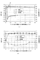
図3は、本実施形態に係るアンテナ装置におけるシミュレーション実験に適用したパラメータを説明するための図である。ここで、図3(a)は、本実施形態に係る導電性素子のアンテナ素子(裏蓋端部)からの離間距離(遠近方向の距離)を説明するための図であり、図3(b)は、本実施形態に係る導電性素子のアンテナ素子(裏蓋端部)に対する相対位置(上下方向の位置)を説明するための図である。また、図4、図5は、本実施形態に係るアンテナ装置における導電性素子の配置と、電磁波の送受信特性との関係(シミュレーション結果)を示す図である。ここで、図4(a)及び図5は、本実施形態に係る導電性素子のアンテナ素子(裏蓋端部)からの離間距離と、電磁波の送受信感度に相当する電磁波の送受信特性と、の関係、及び、同離間距離と共振周波数との関係を示す図である。また、図4(b)は、本実施形態に係る導電性素子のアンテナ素子(裏蓋端部)に対する相対位置と送受信特性との関係、及び、同相対位置と共振周波数との関係を示す図である。 FIG. 3 is a diagram for explaining parameters applied to a simulation experiment in the antenna device according to the present embodiment. Here, FIG. 3A is a diagram for explaining a separation distance (distance in the perspective direction) from the antenna element (back cover end portion) of the conductive element according to the present embodiment, and FIG. ) Is a diagram for explaining the relative position (position in the vertical direction) of the conductive element according to the present embodiment with respect to the antenna element (back cover end). 4 and 5 are diagrams showing the relationship (simulation result) between the arrangement of conductive elements and the transmission / reception characteristics of electromagnetic waves in the antenna device according to this embodiment. Here, FIGS. 4A and 5 show the distance between the conductive element according to the present embodiment from the antenna element (back cover end) and the transmission / reception characteristics of the electromagnetic wave corresponding to the transmission / reception sensitivity of the electromagnetic wave. It is a figure which shows the relationship and the relationship between the separation distance and the resonance frequency. FIG. 4B is a diagram showing the relationship between the relative position of the conductive element according to this embodiment with respect to the antenna element (back cover end) and the transmission / reception characteristics, and the relationship between the relative position and the resonance frequency. It is.
本実施形態においては、次のような条件を有する電子機器(アンテナ装置)を対象にしてシミュレーション実験を実行した。一般に、携帯型の電子機器においては、アンテナ素子の周辺に導電性の部品が配置された構成や、防水性能を高めるため、金属製の裏蓋を備えた構成が採用されている。このような導電性の部品や裏蓋は、アンテナ装置の特性に大きな影響を与えることが知られている。 In the present embodiment, a simulation experiment was performed on an electronic device (antenna device) having the following conditions. In general, in portable electronic devices, a configuration in which conductive parts are arranged around an antenna element and a configuration with a metal back cover are employed in order to improve waterproof performance. It is known that such conductive parts and back covers have a great influence on the characteristics of the antenna device.
そこで、本実施形態においては、実製品に近い条件でシミュレーション実験を行うために、図3(a)、(b)に示すように、上述した電子機器100Aの他面側(図1、図2の下面側)に、金属製の裏蓋が設けられた構成を有する電子機器を対象として各パラメータを設定した。すなわち、本実施形態に係る導電性素子113のアンテナ素子112からの遠近方向の距離(離間距離)として、図3(a)に示すように、筐体110の他面側に設けられた裏蓋115の端部から導電性素子113までの水平方向(図面左右方向)の距離Laを規定した(以下、便宜的に「離間距離La」と記す)。また、本実施形態に係る導電性素子113のアンテナ素子112に対する上下方向の位置(相対位置)として、図3(b)に示すように、筐体110の他面側に設けられた裏蓋115の底面から導電性素子113までの垂直方向(図面上下方向)の距離Haを規定した(以下、便宜的に「相対位置Ha」と記す)。なお、このシミュレーション実験においては、導電性素子113として、断面が1mm角(1mm×1mm)で、延在方向の長さが31.1mmの銅製の部材を用いた。また、アンテナ素子112が送受信する電磁波の周波数をGPSに適用される1.57542GHzに設定した。
Therefore, in the present embodiment, in order to perform a simulation experiment under conditions close to the actual product, as shown in FIGS. 3A and 3B, the other surface side of the
図3(b)に示した導電性素子113の裏蓋115の端部からの相対位置Haを0mmに設定した状態(相対位置Ha=0mm;裏蓋115の底面と面一)で、図3(a)に示した導電性素子113の裏蓋115の端部からの離間距離Laを変えながら、電磁波の放射効率、及び、共振周波数を導出するシミュレーション実験により、図4(a)に示すような結果が得られた。電磁波の放射効率は、その値が大きいほど電磁波の受信感度又は送信効率が高く、電磁波の送受信特性が良好であることを示している。ここで、離間距離Laや相対位置Haを変えたときに、電磁波の放射効率が最も高くなる周波数が変化するため、図4(a)では、各離間距離Laにおいて、この放射効率が最大となる周波数での放射効率の値を「効率」として示し、この放射効率が最大となる周波数(共振周波数)を「周波数」として示している。後述する図4(b)、図5、図6、図13、図15においても同様である。また、図4、図5では、比較のために、導電性素子113を有していない、従来の構造の場合の電磁波の放射効率の値を「従来効率」として示している。図4(a)によれば、離間距離Laを概ね0.2mm以上に設定した場合に、高い放射効率が得られ、特に概ね0.3mmに設定した状態(図中「B」)で放射効率が最大値を示し、離間距離Laが概ね0.2mmから2mmの間で、放射効率が、導電性素子113を有していない従来の場合より高くなる傾向を示した。また、離間距離Laを概ね1.0mm以上に設定した場合に、共振周波数が安定する傾向を示した。
In a state where the relative position Ha from the end of the
なお、図4(a)に示した結果では、離間距離Laが小さい(すなわち、導電性素子113が裏蓋115の端部に近い)ほど、放射効率が高くなる傾向を示したが、極端に小さい場合(離間距離Laが概ね0.1mm)や、導電性素子113が裏蓋115に接触した状態(離間距離Laが0mm)には、放射効率が大幅に劣化する(不安定になる)現象が観測された。また、離間距離Laが小さいほど(離間距離Laが概ね0.5mm以下)、共振周波数が不安定になる現象が観測された。
In addition, in the result shown to Fig.4 (a), although the separation distance La was small (namely, the
次いで、上述したシミュレーション実験の結果(図4(a))に基づいて、高い放射効率が得られるとともに、安定した共振周波数を示すように、導電性素子113を裏蓋115の端部から1.0mm離した状態(離間距離La=1.0mm)で、導電性素子113の裏蓋115の端部からの相対位置Haを変えながら、電磁波の放射効率、及び、共振周波数を導出するシミュレーション実験により、図4(b)に示すような結果が得られた。これによれば、相対位置Haを概ね1mm以上に設定した場合に、高い放射効率が得られ、特に概ね5mmに設定した状態で放射効率が最大値を示し、相対位置Haが概ね1mmから8mmの間で、放射効率が、導電性素子113を有していない場合より高くなる傾向を示した。ここで、相対位置Haを概ね5mmに設定した状態は、アンテナ素子112の直上(図3では左方の対向位置)に導電性素子113を配置した状態に相当する。また、相対位置Haを概ね1.0mm以上に設定した場合に、共振周波数が安定する傾向を示した。
Next, based on the result of the simulation experiment described above (FIG. 4A), the
次いで、上述したシミュレーション実験の結果(図4(b))に基づいて、高い放射効率が得られるとともに、安定した共振周波数を示すように、導電性素子113を裏蓋115の端部から5mmの位置に設定した状態(相対位置Ha=5mm;アンテナ素子112の直上位置)で、導電性素子113の裏蓋115の端部からの離間距離Laを変えながら、電磁波の放射効率、及び、共振周波数を導出するシミュレーション実験により、図5に示すような結果が得られた。これによれば、離間距離Laを概ね1.1mmに設定した状態(図中「C」)で放射効率が最大値を示し、離間距離Laが概ね4mm以下のとき、放射効率が、導電性素子113を有していない場合より高くなる傾向を示した。また、離間距離Laを概ね1.0mm以上に設定した場合に、共振周波数が安定する傾向を示した。なお、図5に示した結果では、離間距離Laが大きい(すなわち、導電性素子113が裏蓋115の端部から遠い)ほど、放射効率が低くなる傾向を示したが、離間距離Laが概ね1mm以下の場合には、放射効率に周期的な変化(図中「D」)が見られ、不安定になる現象が観測された。
Next, based on the result of the simulation experiment described above (FIG. 4B), high radiation efficiency is obtained, and the
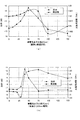
次に、本実施形態に係るアンテナ装置におけるアンテナ素子112の長さ(寸法)と、電磁波の放射効率との関係について説明する。
図6は、本実施形態に係るアンテナ装置における導電性素子の長さと、電磁波の放射効率との関係(シミュレーション結果)を示す図である。ここで、図6(a)は、本実施形態に係る導電性素子を裏蓋に接触させた状態(導通状態)における、導電性素子の長さと放射効率との関係、及び、同長さと共振周波数との関係を示す図である。また、図6(b)は、本実施形態に係る導電性素子を裏蓋から離間させた状態(非導通状態)における、導電性素子の長さと放射効率との関係、及び、同長さと共振周波数との関係を示す図である。
Next, the relationship between the length (dimension) of the
FIG. 6 is a diagram illustrating a relationship (simulation result) between the length of the conductive element and the radiation efficiency of the electromagnetic wave in the antenna device according to the present embodiment. Here, FIG. 6A shows the relationship between the length of the conductive element and the radiation efficiency in a state where the conductive element according to the present embodiment is in contact with the back cover (conductive state), and the length and resonance. It is a figure which shows the relationship with a frequency. FIG. 6B shows the relationship between the length of the conductive element and the radiation efficiency in a state where the conductive element according to this embodiment is separated from the back cover (non-conductive state), and the length and resonance. It is a figure which shows the relationship with a frequency.
図3(b)に示した相対位置Haを0mmに設定し、かつ、図3(a)に示した離間距離Laを0mmに設定した状態(導電性素子113が裏蓋115に接触した状態)で、上述したシミュレーション実験と同等の形状、及び、延在方向の長さ(31.1mm)を有する導電性素子113を基準として、その長さを変えながら、電磁波の放射効率、及び、共振周波数を導出するシミュレーション実験により、図6(a)に示すような結果が得られた。これによれば、導電性素子113の長さを概ね75mm以上に長く設定した場合、放射効率が劣化する現象が観測された。また、導電性素子113の長さが長いほど(概ね50mm以上)共振周波数が比較的大きく変化する現象が観測された。
The relative position Ha shown in FIG. 3B is set to 0 mm, and the separation distance La shown in FIG. 3A is set to 0 mm (the
これに対して、図3(a)に示した離間距離Laを0.5mmに設定した状態(導電性素子113を裏蓋115の端部から0.5mm離した状態)で、導電性素子113の延在方向の長さを変えながら、電磁波の放射効率、及び、共振周波数を導出するシミュレーション実験により、図6(b)に示すような結果が得られた。これによれば、導電性素子113の長さを概ね75mm以上に長く設定した場合であっても、高い放射効率が得られ、特に概ね75mmに設定した状態で放射効率が最大値を示した。また、導電性素子113の長さが長いほど(概ね75mm以上)共振周波数が安定する傾向を示した。ここで、図6(a)、(b)に示した導電性素子113の延在方向の長さは、基準値(初期値)が31.1mmに設定されているので、導電性素子113の全長は概ね106mm(=31.1+75)になる。一方、GPSに適用される電磁波の周波数は1.57542GHzであるので、上記の導電性素子113の全長106mmは、この場合の電磁波の波長λの概ね1/2(=λ/2)に相当する。
On the other hand, in the state where the separation distance La shown in FIG. 3A is set to 0.5 mm (the state where the
なお、図示を省略したが、発明者らは、同様のシミュレーション実験により、放射効率の導出に用いた電磁波の波長λの概ね1/2n(n=0、1、2、3、・・・)の長さに対応するように、上記の導電性素子113の全長を設定することにより、当該長さの近傍で概ね高い放射効率及び安定した共振周波数が得られる傾向があることを確認した。
Although not shown, the inventors conducted a similar simulation experiment to approximately ½ n (n = 0, 1, 2, 3,...) Of the wavelength λ of the electromagnetic wave used to derive the radiation efficiency. It was confirmed that, by setting the total length of the
したがって、上述した各シミュレーション実験の結果に基づいて、アンテナ素子に対する導電性素子の配置や、当該導電性素子の形状及び寸法(長さ)を適切に設定することにより、アンテナ素子により送受信する電磁波の周波数で共振して、電磁波に対して良好に共振することができるアンテナ装置を実現することができる。 Therefore, based on the result of each simulation experiment described above, by appropriately setting the arrangement of the conductive element with respect to the antenna element and the shape and size (length) of the conductive element, the electromagnetic wave transmitted and received by the antenna element can be determined. An antenna device that resonates at a frequency and can resonate well with electromagnetic waves can be realized.
次に、上述したシミュレーション実験の結果に基づいて高い放射効率及び安定した共振周波数が実現されるように、配置や形状、寸法が設定された導電性素子を用いて、本実施形態に係るアンテナ装置の放射特性について説明する。ここでは、アンテナ装置に本実施形態に係る導電性素子を備えていない構成(以下、「比較例」と記す)を用いて、比較検証する。 Next, the antenna device according to the present embodiment using the conductive elements whose arrangement, shape, and dimensions are set so that high radiation efficiency and a stable resonance frequency are realized based on the result of the simulation experiment described above. The radiation characteristics will be described. Here, comparative verification is performed using a configuration in which the antenna device does not include the conductive element according to the present embodiment (hereinafter referred to as “comparative example”).
図7は、本実施形態に係るアンテナ装置における放射特性を示す図(シミュレーション結果)である。図7(a)は、本実施形態の比較例となるアンテナ装置における放射特性を示す図であり、図7(b)は、本実施形態に係るアンテナ装置における放射特性を示す図である。 FIG. 7 is a diagram (simulation result) showing radiation characteristics in the antenna device according to the present embodiment. FIG. 7A is a diagram illustrating a radiation characteristic in an antenna device as a comparative example of the present embodiment, and FIG. 7B is a diagram illustrating a radiation characteristic in the antenna device according to the present embodiment.
まず、上述した電子機器100Aにおいて、筐体110の側面に導電性素子113が設けられていない構成を有する比較例における電磁波の放射特性について説明する。比較例において、GPSに適用される1.57542GHz(概ね1.6GHz)の周波数の電磁波を、直線偏波型のアンテナ素子を用いて送受信した際の放射特性を導出するシミュレーション実験を行った結果、図7(a)に示すような放射パターンが得られた。ここで、図1に示した電子機器100Aを参照して比較例について説明すると、図7(a)は、筐体110において、表示部111が設けられた一面(又は他面)を含む平面における全周方向(0〜360°)の放射パターンである。このシミュレーション実験により得られた、比較例の平均利得は−6.35dBiであった。
First, in the
これに対して、筐体110の内部に設けられたアンテナ素子112に対向する側面に、上述したシミュレーション実験の結果に基づいて、高い放射効率及び安定した共振周波数が実現されるように、導電性素子113が適切な配置や形状、寸法に設定された本実施形態において、上述した比較例と同一条件で放射特性を導出するシミュレーション実験を行った結果、図7(b)に示すような放射パターンが得られた。このシミュレーション実験により得られた、本実施形態の平均利得は−5.9dBiであった。このことから、本実施形態に係る構成によれば、導電性素子113が設けられていない構成(比較例)に比較して、利得が改善(概ね0.45dBi)することが判明した。
On the other hand, on the side surface facing the
本実施形態における放射特性の改善効果について検証する。一般に、腕時計型端末等の小型の電子機器においては、筐体が小型や薄型で密閉構造であるため、内部に実装されるアンテナ装置は、十分な放射抵抗を得ることができず、また、必要な接地(グラウンド)板もサイズを小さくしなければならない。そのため、アンテナ装置における放射効率が悪く、給電される電力の多くが熱として消費され、この消費エネルギーの多くが電子機器の筐体周辺に近傍電磁波を発生させたり、筐体に意図しない多量のリーク電流(漏れ電流)として滞在したりすることになる。これにより、本来の電磁波の送受信に直接関与する電磁波が影響を受けて、その放射特性が悪化し、電子機器の通信状態が不安定になるという問題を有していた。 The effect of improving the radiation characteristics in this embodiment will be verified. In general, in a small electronic device such as a wristwatch type terminal, the housing is small and thin and has a hermetically sealed structure. Therefore, the antenna device mounted inside cannot obtain sufficient radiation resistance and is necessary. The grounding plate must also be reduced in size. Therefore, the radiation efficiency of the antenna device is poor, and much of the supplied power is consumed as heat, and much of this energy consumption generates nearby electromagnetic waves around the casing of the electronic device, or a large amount of unintended leakage in the casing. Or stay as current (leakage current). As a result, the electromagnetic waves directly involved in the transmission and reception of the original electromagnetic waves are affected, the radiation characteristics are deteriorated, and the communication state of the electronic device becomes unstable.
そこで、本実施形態においては、筐体110の内部に設けられたアンテナ素子112に対向する側面に導電性素子113を配置した構成を適用している。これにより、導電性素子113により、上述した近傍電磁波やリーク電流を生じるエネルギーを効率的に受け、アンテナ素子112から放射された電磁波に対して共振して、筐体110の外部方向に効率良く再放射させることができる。したがって、本実施形態によれば、図3に示したように、平均利得を改善させて放射特性を向上させたアンテナ装置を実現することができる。
Therefore, in the present embodiment, a configuration in which the
<第1の実施形態の変形例>
次に、上述した第1の実施形態の変形例について説明する。
図8は、第1の実施形態に係るアンテナ装置を適用した電子機器の変形例を示す概略構成図である。ここで、図8(a)は、本実施形態に係る電子機器の外観構成を示す斜視図であり、図8(b)は、図8(a)に示した電子機器におけるVIIIB−VIIIB線(本明細書においては図8中に示したローマ数字の「8」に対応する記号として便宜的に「VIII」を用いる。以下同じ。)に沿って矢視した側面を示す図であり、図8(c)は、図8(a)に示した電子機器におけるVIIIC−VIIIC線に沿って矢視した側面を示す図である。図9は、第1の実施形態に係るアンテナ装置を適用した電子機器の他の変形例を示す概略構成図である。なお、図8、図9においても、図示を明瞭にするために、導電性素子に便宜的にハッチングを施して示した。また、上述した実施形態と同等の構成については同一の符号を付して説明を簡略化する。
<Modification of First Embodiment>
Next, a modification of the above-described first embodiment will be described.
FIG. 8 is a schematic configuration diagram illustrating a modified example of the electronic apparatus to which the antenna device according to the first embodiment is applied. Here, FIG. 8A is a perspective view showing an external configuration of the electronic apparatus according to the present embodiment, and FIG. 8B is a line VIIIB-VIIIB in the electronic apparatus shown in FIG. In the present specification, “VIII” is used as a symbol corresponding to the Roman numeral “8” shown in FIG. 8 for the sake of convenience. The same shall apply hereinafter.) FIG. (C) is a figure which shows the side surface which looked at the arrow along the VIIIC-VIIIC line | wire in the electronic device shown to Fig.8 (a). FIG. 9 is a schematic configuration diagram illustrating another modification of the electronic device to which the antenna device according to the first embodiment is applied. 8 and 9 also show the conductive elements hatched for the sake of convenience for the sake of clarity. Further, the same components as those in the above-described embodiment are denoted by the same reference numerals, and the description is simplified.
上述した第1の実施形態においては、筐体110の内部に設けられたアンテナ素子112に対向する筐体110の一側面にのみ、導電性素子113を設けた構成を示した。本実施形態の変形例においては、例えば図8(a)〜(c)に示すように、アンテナ素子112に対向する側面(図8(a)手前側の側面)を含む、筐体110の4側面の各々に個別に導電性素子113a〜113dを設けた構成を有している。
In the first embodiment described above, the configuration in which the
このような構成を有するアンテナ装置を備えた電子機器100Aによれば、上述した実施形態と同様に、電磁波の放射特性(アンテナ特性)を向上させることができる。特に、筐体110の各側面に導電性素子113が設けられているので、アンテナ素子112から放射され、筐体110の内部に閉じ込められた電磁波を、4方向に配置された導電性素子113より受けて励起し、筐体110の外部に再放射することができるので、電磁波の放射特性をより向上させることができる。
According to the
また、本実施形態においては、導電性素子113が筐体110の各側面に露出して設けられているので、導電性素子113の素材や形状等を任意に設定することにより、筐体110の装飾やデザインとしての統一感を持たせることができ、より多様なデザインの創出に寄与することができる。
In the present embodiment, since the
なお、図8においては筐体の4側面の全てに導電性素子を個別に設けた構成を示したが、本発明はこれに限定されるものではない。例えば図9(a)に示すように、筐体110の対向する2側面(図ではアンテナ素子112に近接する側面と、それに対向する側面)に個別に導電性素子113a、113bを設けた構成を有しているものであってもよい。また、例えば図9(b)に示すように、筐体の3側面(図ではアンテナ素子112に近接する側面と、それに隣接する両側面)に個別に導電性素子113a、113c、113dを設けた構成を有しているものであってもよい。さらに、例えば図9(c)に示すように、相互に隣接する任意の複数の側面(図ではアンテナ素子112に近接する側面と、それに隣接する両側面の、計3側面)に連続して一体的に形成された導電性素子113eを設けた構成を有しているものであってもよい。
Although FIG. 8 shows a configuration in which conductive elements are individually provided on all four side surfaces of the housing, the present invention is not limited to this. For example, as shown in FIG. 9A, a configuration in which conductive elements 113a and 113b are individually provided on two opposing side surfaces of the housing 110 (the side surface close to the
<第2の実施形態>
次に、本発明に係るアンテナ装置を適用した電子機器の第2の実施形態について説明する。
<Second Embodiment>
Next, a second embodiment of an electronic apparatus to which the antenna device according to the present invention is applied will be described.
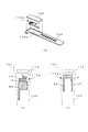
図10は、第2の実施形態に係る電子機器を示す概略構成図である。ここで、図10(a)は、本実施形態に係る電子機器の外観構成を示す斜視図であり、図10(b)は、図10(a)に示した電子機器をベルト部側から見た側面を示す図であり、図10(c)は、図10(b)に示した電子機器におけるXC−XC線(本明細書においては図10中に示したローマ数字の「10」に対応する記号として便宜的に「X」を用いる。)に沿った断面構造を示す概略図である。なお、図10(a)、(b)においては、図示を明瞭にするために、導電性素子に便宜的にハッチングを施して示した。また、上述した第1の実施形態と同等の構成については同一の符号を付して説明を簡略化する。図11は、本実施形態に適用される導電性素子を示す概略構成図である。ここで、図11(a)、(b)は、ベルト部への導電性素子の組み付け構造を示す概略図であり、図11(c)〜(e)は、導電性素子の他の平面形状を示す概略図である。 FIG. 10 is a schematic configuration diagram illustrating an electronic apparatus according to the second embodiment. Here, FIG. 10A is a perspective view showing an external configuration of the electronic apparatus according to the present embodiment, and FIG. 10B is a view of the electronic apparatus shown in FIG. FIG. 10C corresponds to the XC-XC line in the electronic device shown in FIG. 10B (corresponding to the Roman numeral “10” shown in FIG. 10 in this specification). For the sake of convenience, “X” is used as a symbol to indicate the cross-sectional structure). In FIGS. 10A and 10B, the conductive elements are hatched for the sake of convenience for the sake of clarity. Further, the same components as those in the first embodiment described above are denoted by the same reference numerals, and the description is simplified. FIG. 11 is a schematic configuration diagram showing a conductive element applied to this embodiment. Here, FIGS. 11A and 11B are schematic views showing the assembly structure of the conductive element to the belt portion, and FIGS. 11C to 11E are other planar shapes of the conductive element. FIG.
上述した第1の実施形態においては、単体の筐体110からなる電子機器110Aにおいて、筐体110の1乃至複数の側面に導電性素子113を設けた構成を示した。第2の実施形態においては、機器本体に一体的にベルト部が付設された腕時計型の電子機器において、当該ベルト部に導電性素子が設けられた構成を有している。
In the above-described first embodiment, the configuration in which the
具体的には、第2の実施形態に係る電子機器100Bは、例えば図10(a)〜(c)に示すように、上述した第1の実施形態に示した電子機器100Aと同等の構成を有する機器本体(筐体)101と、機器本体101を手首等の人体に装着するためのベルト部(バンド部材)102と、を備えた腕時計型の構成を有している。
Specifically, the
機器本体101は、上述した電子機器100Aと同様に、内部にアンテナ素子112が設けられている。ここで、本実施形態に係る機器本体101においては、アンテナ素子112に対向する機器本体101の側面には、導波器として機能する導電性素子は設けられていない。
The device
ベルト部102は、ウレタン樹脂等の絶縁性材料からなる帯状部材より構成され、機器本体101の対向する一対の側面近傍であって、機器本体101の他面側(図面下面側)に、それぞれ取り付けられている。また、機器本体101の内部に設けられたアンテナ素子112に対向する、ベルト部102の任意の領域には、所定の平面形状を有する導電性素子113fが設けられている。ここで、導電性素子113fは、例えば導電性の薄板や薄膜からなり、図11(a)、(b)に示すように、ベルト部102に設けられた凹状の収納部102aに導電性素子113fを収納した状態で、例えばベルト部102と同等の素材のカバー部材103により収納部102aを閉止することにより、ベルト部102の内部に組み込まれる。
The
導電性素子113fの平面形状は、例えば図10(a)、(b)に示すように、機器本体101側を基部とする幅広部を有し、ベルト部102の先端方向に向かって幅が狭くなるように形成された一対の突出部が設けられている。このような導電性素子113fにおいて、幅広部は、機器本体101の内部に設けられるアンテナ素子112の延在方向(又は、機器本体101の側面)に対して、所定の離間距離を有して対向するように延在し、アンテナ素子112から放射される電磁波を受ける受け側の辺(第1の辺)Saを有している。また、突出部は、ベルト部102の延在方向に沿って突出し、上記受け側の辺Saにおいて受けた電磁波に対して共振して再放射するための放射側の辺(第2の辺)Sbを有している。そして、本実施形態においては、導電性素子113fの受け側の辺Saと放射側の辺Sbは、略垂直になるように設定されている。
For example, as shown in FIGS. 10A and 10B, the planar shape of the conductive element 113f has a wide portion whose base is the device
ここで、本実施形態においては、導電性素子113fの受け側の辺Saの長さが、例えばアンテナ素子112により送受信される電磁波の波長λの1/8(=λ/8)に設定され、放射側の辺Sbの長さが、例えば上記波長λの1/4(=λ/4)に設定されている。これにより、導電性素子113fは、上述した第1の実施形態と同様に、アンテナ素子112及びその周辺から放射される電磁波を効率良く受け、一旦電流に変換した後、共振した電磁波を再び空間に放射する導波器として機能する。
Here, in the present embodiment, the length of the side Sa on the receiving side of the conductive element 113f is set to 1/8 (= λ / 8) of the wavelength λ of the electromagnetic wave transmitted and received by the
このような導電性素子113fは、導電性の薄板や薄膜を所定の平面形状にパターニングすることにより形成される。ここで、導電性素子113fは、上述した第1の実施形態と同様に、導電性塗料を塗布する手法や、金属蒸着法、スパッタリング法等を適用して形成することができる。 Such a conductive element 113f is formed by patterning a conductive thin plate or thin film into a predetermined planar shape. Here, the conductive element 113f can be formed by applying a conductive coating method, a metal vapor deposition method, a sputtering method, or the like, as in the first embodiment described above.
なお、導電性素子113fは、図10(a)、(b)又は図11(a)、(b)に示した形状に限定されるものではなく、上述したように、アンテナ素子112から放射される電磁波を受けて励振し、外部に再放射することができる形状や寸法を有するものであれば、他の平面形状を有するものであってもよい。具体的には、導電性素子113fは、例えば図11(c)に示すように、略均一な幅の、略コの字型の平面形状を有するものや、例えば図11(d)に示すように、図10(a)、(b)に示した導電性素子において、基部近傍にまで切れ込みを形成した略U字型の平面形状を有するもの、例えば図11(e)に示すように、図10(a)、(b)に示した導電性素子において、基部の幅広部から略均一な幅の、単一の突出部が形成された平面形状を有するもの等を、良好に適用することができる。
Note that the conductive element 113f is not limited to the shape shown in FIGS. 10A and 10B or FIGS. 11A and 11B, and is radiated from the
また、ベルト部102の任意の領域に、導電性素子113fを設けるための構成についても、図11(a)、(b)に示した組み込み方法に限定されるものではなく、導波器としての機能を実現することができるものであれば、他の構造を有するものであってもよい。具体的には、導電性素子113fは、上述した第1の実施形態に示したように、絶縁性材料からなるベルト部102の表面に、導電性塗料を塗布する手法や、導電性の薄膜を貼り付ける手法、金属蒸着法やスパッタリング法等を適用して形成するものであってもよい。また、導電性素子113fは、インサート成形法等を用いてベルト部102に導電性部材が埋め込まれているものであってもよいし、2色成形法等を用いてベルト部102に導電性樹脂が一体的に形成されているものであってもよい。
Further, the configuration for providing the conductive element 113f in an arbitrary region of the
また、導電性素子113fは、図10に示したように、機器本体101に付設された一対のベルト部102のうちの一方のみ(アンテナ素子112に近接する側のベルト部)に設けた構成に限定されるものではなく、一対のベルト部102の双方に設けた構成を有するものであってもよい。このとき、各々のベルト部102に設けられる導電性素子113fの形状や寸法等を、適切に設定することにより、電磁波の放射特性をさらに向上させることができる。
Further, as shown in FIG. 10, the conductive element 113 f is provided in only one of the pair of
このような構成を有するアンテナ装置を備えた電子機器100Bによれば、上述した第1の実施形態と同様に、機器本体101に内蔵されたアンテナ素子112に対向するように、ベルト部102に導電性素子113fを配置することができるので、平均利得を改善させて放射特性を向上させたアンテナ装置を実現することができる。特に、導電性素子113fを機器本体101に付設されたベルト部102の任意の領域に設けることができるので、導電性素子113fの形状の設計自由度を高めることができ、伝送線路を適切に設計することにより、円偏波に対応したアンテナ装置や、指向性制御が可能なアンテナ装置を実現することができる。また、この場合、導電性素子113fを電子機器100Bの装飾やデザインの一部として組み入れることができ、商品価値を一層高めることができる。また、導電性素子113fをベルト部102に設けることにより、機器本体101の設計を変更する必要がないので、機器本体の製造方法やコストに影響を与えることなく、ベルト部102のような付属の部品への適用のみで放射特性を向上させることができる。
According to the
次に、本実施形態における効果(電磁波の放射特性の改善効果)について、シミュレーション実験の結果を示して具体的に説明する。
まず、本実施形態に係るアンテナ装置におけるアンテナ素子112に対する導電性素子113の形状及び配置時の傾斜角度と、電磁波の放射効率との関係について説明する。
Next, the effect in this embodiment (the effect of improving the radiation characteristics of electromagnetic waves) will be specifically described by showing the results of a simulation experiment.
First, the relationship between the shape of the
図12は、本実施形態に係るアンテナ装置におけるシミュレーション実験に適用したパラメータを説明するための図である。ここで、図12(a)、(d)は、本実施形態に係る導電性素子が直線形状を有し、機器本体の側面の延在方向に沿って配置された状態を示す概略斜視図であり、図12(b)、(e)は、導電性素子が屈曲形状を有し、傾斜角度0°で配置された状態を示す概略斜視図であり、図12(c)、(f)は、導電性素子が屈曲形状を有し、傾斜角度60°で配置された状態を示す概略斜視図である。また、図13は、本実施形態に係るアンテナ装置における導電性素子の形状及び配置時の傾斜角度と、電磁波の放射効率との関係(シミュレーション結果)を示す図である。 FIG. 12 is a diagram for explaining parameters applied to a simulation experiment in the antenna device according to the present embodiment. Here, FIGS. 12A and 12D are schematic perspective views showing a state in which the conductive element according to the present embodiment has a linear shape and is arranged along the extending direction of the side surface of the apparatus main body. FIGS. 12B and 12E are schematic perspective views showing a state in which the conductive element has a bent shape and is arranged at an inclination angle of 0 °. FIGS. 12C and 12F are views. FIG. 3 is a schematic perspective view showing a state where the conductive element has a bent shape and is arranged at an inclination angle of 60 °. FIG. 13 is a diagram showing the relationship (simulation result) between the shape of the conductive element in the antenna device according to this embodiment, the inclination angle at the time of arrangement, and the radiation efficiency of electromagnetic waves.
本実施形態においては、図12(a)〜(f)に示すような構成を有する電子機器(アンテナ装置)を対象にしてシミュレーション実験を実行した。すなわち、図12(a)、(d)に示すアンテナ装置は、上述した第1の実施形態において検証したシミュレーション実験の結果に基づいて、アンテナ素子112に対する配置や、その形状及び寸法(長さ)が適切に設定された直線形状の導電性部材から構成される導電性素子113を備えている。また、図12(b)、(e)に示すアンテナ装置は、図12(a)、(d)に示した直線形状の導電性部材を、所定の位置で直角に折り曲げてコの字状に形成し、さらに傾斜角度0°で配置した導電性素子113を備えている。また、図12(c)、(f)に示すアンテナ装置は、図12(b)、(e)に示したコの字状の導電性部材を、傾斜角度60°で配置した導電性素子113を備えている。なお、このシミュレーション実験においては、導電性素子113として、断面が1mm角(1mm×1mm)で、延在方向の長さが106.1mm(=31.1+75)の銅製の部材を用い、アンテナ素子112を用いて送受信する電磁波の周波数として、GPSに適用される1.57542GHzに設定した。
In the present embodiment, a simulation experiment was performed on an electronic device (antenna device) having a configuration as illustrated in FIGS. That is, the antenna device shown in FIGS. 12A and 12D is arranged with respect to the
図10に示した構成と同様に、機器本体101に一体的に付設されたベルト部102の任意の領域(ここでは機器本体101側の端部)に、アンテナ素子112に対向するように導電性素子113を配置した状態(概ね上述した相対位置Haが0mmとなる裏蓋115と面一の状態)で、図12(a)〜(c)に示すように、導電性素子113を直線形状とした場合、及び、導電性素子113をコの字型に直角に折り曲げて、さらに傾斜角度を0°、60°に設定した場合の、電磁波の放射効率、及び、共振周波数を導出するシミュレーション実験により、図13の左側に示すグラフのような結果が得られた。
Similar to the configuration shown in FIG. 10, a conductive region is provided so as to face the
また、上述した第1の実施形態に示した各シミュレーション実験の結果に基づいて、高い放射効率及び安定した共振周波数を示した、アンテナ素子112の直上に導電性素子113を配置した状態(図3に示した左方の対向位置で概ね相対位置Haが5mmとなる状態)で、図12(d)〜(e)に示すように、導電性素子113を直線形状とした場合、及び、導電性素子113をコの字型に直角に折り曲げて、さらに傾斜角度を0°、60°に設定した場合の、電磁波の放射効率、及び、共振周波数を導出するシミュレーション実験により、図13の右側に示すグラフのような結果が得られた。
In addition, based on the results of the simulation experiments shown in the first embodiment described above, the
これらのシミュレーション実験の結果によれば、導電性素子113をコの字型に折り曲げた屈曲形状とした場合には、傾斜角度を60°に設定することにより、導電性素子113を直線形状とした場合と略同等の高い受信感度が得られた。また、屈曲形状の導電性素子113の傾斜角度に関わらず、略同等の共振周波数を示した。
According to the results of these simulation experiments, when the
次に、本実施形態に係るアンテナ装置におけるアンテナ素子112の配置時の離間距離と、電磁波の放射効率との関係について説明する。
図14は、本実施形態に係るアンテナ装置におけるシミュレーション実験に適用したパラメータを説明するための図である。ここで、図14(a)、(b)は、本実施形態に係る導電性素子をベルト部端部の任意の領域に配置した場合に、高い放射効率が得られるとともに、安定した共振周波数を示す最適位置を初期位置として、当該初期位置からの変位を示す図である。また、図14(c)、(d)は、導電性素子をアンテナ素子の直上に配置した場合に、高い放射効率が得られるとともに、安定した共振周波数を示す最適位置を初期位置として、当該初期位置からの変位を示す図である。また、図15は、本実施形態に係るアンテナ装置における導電性素子の配置と、電磁波の放射効率との関係(シミュレーション結果)を示す図である。ここで、図15(a)は、本実施形態に係る導電性素子をベルト部端部に配置した状態における、上記初期位置からの変位(高い放射効率が得られるとともに、安定した共振周波数を示す最適位置からの距離)と放射効率との関係、及び、同変位と共振周波数との関係を示す図である。また、図15(b)は、本実施形態に係る導電性素子をアンテナ素子の直上に配置した状態(非導通状態)における、上記初期位置からの変位(最適位置からの距離)と放射効率との関係、及び、同変位と共振周波数との関係を示す図である。
Next, the relationship between the separation distance when the
FIG. 14 is a diagram for explaining parameters applied to a simulation experiment in the antenna device according to the present embodiment. Here, FIGS. 14A and 14B show that when the conductive element according to this embodiment is arranged in an arbitrary region at the end of the belt portion, high radiation efficiency is obtained and a stable resonance frequency is obtained. It is a figure which shows the displacement from the said initial position by making the optimal position shown into an initial position. 14 (c) and 14 (d) show that when the conductive element is arranged immediately above the antenna element, high radiation efficiency is obtained, and the initial position is the optimum position showing a stable resonance frequency. It is a figure which shows the displacement from a position. FIG. 15 is a diagram showing a relationship (simulation result) between the arrangement of conductive elements and the radiation efficiency of electromagnetic waves in the antenna device according to the present embodiment. Here, FIG. 15A shows the displacement from the initial position in the state where the conductive element according to the present embodiment is disposed at the end portion of the belt (high radiation efficiency is obtained and a stable resonance frequency is obtained. It is a figure which shows the relationship between the distance from the optimal position) and radiation efficiency, and the relationship between the displacement and resonance frequency. FIG. 15B shows the displacement from the initial position (distance from the optimal position) and the radiation efficiency in a state where the conductive element according to the present embodiment is disposed immediately above the antenna element (non-conductive state). It is a figure which shows the relationship of these, and the relationship between the displacement and resonance frequency.
機器本体101に一体的に付設されたベルト部102の端部の任意の領域に、アンテナ素子112に対向するように導電性素子113を配置し、さらに傾斜角度を60°に設定した状態で、図14(a)、(b)に示すように、導電性素子113を上記傾斜角度で機器本体101から遠ざかる方向に移動させて、初期位置からの変位Baを変えながら、GPSに適用される1.57542GHzの周波数を有する電磁波の放射効率、及び、共振周波数を導出するシミュレーション実験により、図15(a)に示すような結果が得られた。これによれば、変位Baが大きくなるほど(導電性素子113を機器本体101から離すほど)、放射効率が顕著に低下する傾向を示した。また、変位Baを概ね3mm以上に設定した場合に、共振周波数が安定する傾向を示した。
In a state where the
また、導電性素子113をアンテナ素子112の直上に配置し、さらに傾斜角度を60°に設定した状態で、図14(c)、(d)に示すように、導電性素子113を上記傾斜角度で機器本体101から遠ざかる方向に移動させて、初期位置からの変位Baを変えながら、同一条件で電磁波の放射効率、及び、共振周波数を導出するシミュレーション実験により、図15(b)に示すような結果が得られた。これによれば、変位Baが比較的低く設定されている場合(概ね3mm以下)には比較的高い放射効率が得られ、変位Baが大きくなるほど、放射効率が低下する傾向を示した。また、変位Baが大きくなるほど、共振周波数が安定する傾向を示した。
Further, with the
なお、図示を省略したが、発明者らは、同様のシミュレーション実験により、導電性素子の形状を、アンテナ素子112により送受信される電磁波の波長に基づいて、コの字型、又は、これに類似する形状(すなわち、アンテナ素子112からの電磁波の受け側となる辺と、励振された電磁波の放射側となる辺が略直角に形成された任意の平面形状;図11(c)〜(e)参照)設定することにより、概ね高い放射効率及び安定した共振周波数が得られる傾向があることを確認した。
Although not shown, the inventors conducted a similar simulation experiment to determine the shape of the conductive element based on the wavelength of electromagnetic waves transmitted and received by the
したがって、上述した各シミュレーション実験の結果に基づいて、アンテナ素子に対する導電性素子の配置や傾斜角度、当該導電性素子の形状及び寸法(長さ)を適切に設定することにより、アンテナ素子により送受信する電磁波の周波数で共振して、電磁波に対して良好に共振することができるアンテナ装置を実現することができる。 Therefore, transmission / reception is performed by the antenna element by appropriately setting the arrangement and inclination angle of the conductive element with respect to the antenna element, and the shape and size (length) of the conductive element based on the result of each simulation experiment described above. An antenna device that resonates at the frequency of the electromagnetic wave and can resonate well with the electromagnetic wave can be realized.
次に、上述したシミュレーション実験の結果に基づいて、高い放射効率及び安定した共振周波数が実現されるように、配置や傾斜角度、形状、寸法が設定された導電性素子を用いて、本実施形態に係るアンテナ装置の放射特性について説明する。ここでは、機器本体101に付設されたベルト部102に本実施形態に係る導電性素子を備えていない構成(以下、「比較例」と記す)を用いて、比較検証する。
Next, based on the result of the simulation experiment described above, the present embodiment uses a conductive element whose arrangement, inclination angle, shape, and dimensions are set so that high radiation efficiency and a stable resonance frequency are realized. The radiation characteristics of the antenna device according to the above will be described. Here, the
図16は、本実施形態の比較例となるアンテナ装置における放射特性を示す図(シミュレーション結果)であり、図17は、本実施形態に係るアンテナ装置における放射特性を示す図(シミュレーション結果)である。 FIG. 16 is a diagram (simulation result) showing a radiation characteristic in an antenna device as a comparative example of the present embodiment, and FIG. 17 is a diagram (simulation result) showing a radiation characteristic in the antenna device according to the present embodiment. .
まず、上述した電子機器100Bにおいて、機器本体101に付設されたベルト部102に導電性素子113fが設けられていない構成を有する比較例における電磁波の放射特性について説明する。比較例において、GPSに適用される1.57542GHz(概ね1.6GHz)の周波数の電磁波を、直線偏波型のアンテナ素子を用いて送受信した際の放射特性を実測した結果、図16(a)〜(c)に示すような放射パターンが得られた。このシミュレーション実験により得られた、比較例の平均利得は−8.775dBiであった。
First, in the
ここで、図10(a)に示した電子機器100Bを参照して比較例について説明すると、図16(a)は、機器本体101において、表示部111が設けられた一面(図面上面)を含むX−Y平面における放射パターンを示す。ここでは、機器本体101の上記一面の平面形状の中心を基準として、導電性素子113fが設けられたベルト部102が付設された方向(図10(a)の手前方向;腕時計の場合には6時方向)をX軸方向と規定し、また、このX軸に直交する方向(図10(a)の左方向;腕時計の場合には9時方向)をY軸方向と規定した場合のX−Y平面における放射パターンを示す。図16(a)において、放射パターンPCxyは、X−Y平面内の全周方向(0〜360°)における放射成分を示し、また、放射パターンPDxyは、X−Y平面に直交するZ軸方向(図10(a)の下方向;腕時計の場合には手首方向)を含む放射成分のうち、X−Y平面に投影される放射成分である。
Here, a comparative example will be described with reference to the
また、図16(b)は、機器本体101において、上記のX−Y平面に直交するY−Z平面(腕時計の場合には3時−9時方向(Y軸)を通り、X−Y平面に直交する平面)における放射パターンを示す。ここで、図16(b)において、放射パターンPCyzは、Y−Z平面内の全周方向における放射成分を示し、また、放射パターンPDyzは、Y−Z平面に直交するX軸方向を含む放射成分のうち、Y−Z平面に投影される放射成分である。 FIG. 16B shows the Y-Z plane orthogonal to the XY plane (in the case of a wristwatch, passing through the 3 o'clock to 9 o'clock direction (Y axis) in the device main body 101). The radiation pattern in a plane orthogonal to the) is shown. Here, in FIG. 16B, the radiation pattern PCyz indicates a radiation component in the entire circumferential direction in the YZ plane, and the radiation pattern PDyz includes radiation including the X-axis direction orthogonal to the YZ plane. Among the components, it is a radiation component projected onto the YZ plane.
また、図16(c)は、機器本体101において、上記のX−Y平面に直交するZ−X平面(腕時計の場合には6時−12時方向(X軸)を通り、X−Y平面に直交する平面)における放射パターンを示す。ここで、図16(b)において、放射パターンPCzxは、Z−X平面内の全周角度における放射成分を示し、また、放射パターンPDzxは、Z−X平面に直交するY軸方向を含む放射成分のうち、Z−X平面に投影される放射成分である。
FIG. 16C shows the Z-X plane orthogonal to the XY plane (in the case of a wristwatch, passing through the 6 o'clock to 12 o'clock direction (X axis) in the device
これに対して、機器本体101に付設されたベルト部102に、上述したシミュレーション実験の結果に基づいて、高い放射効率及び安定した共振周波数が実現されるように、導電性素子113fが適切な配置や傾斜角度、形状、寸法に設定された本実施形態において、上述した比較例と同一条件でシミュレーション実験を行った結果、図17(a)〜(c)に示すような放射パターンが得られた。このシミュレーション実験により得られた、本実施形態の平均利得は−5.917dBであった。このことから、本実施形態に係る構成によれば、導電性素子113fが設けられていない構成(比較例)に比較して、利得が大幅に改善(概ね2.858dBi)することが判明した。
On the other hand, the conductive element 113f is appropriately disposed on the
なお、図17(a)は、図10(a)に示した電子機器100Bの機器本体101において、X−Y平面における放射パターンを示す。ここで、図17(a)において、放射パターンPAxyは、X−Y平面内の全周方向(0〜360°)における放射成分を示し、また、放射パターンPBxyは、X−Y平面に直交するZ軸方向を含む放射成分のうち、X−Y平面に投影される放射成分である。
Note that FIG. 17A shows a radiation pattern in the XY plane in the device
また、図17(b)は、機器本体101において、上記のX−Y平面に直交するY−Z平面における放射パターンを示す。ここで、図17(b)において、放射パターンPAyzは、Y−Z平面内の全周方向における放射成分を示し、また、放射パターンPByzは、Y−Z平面に直交するX軸方向を含む放射成分のうち、Y−Z平面に投影される放射成分である。
FIG. 17B shows a radiation pattern in the YZ plane orthogonal to the XY plane in the device
また、図17(c)は、機器本体101において、上記のX−Y平面に直交するZ−X平面における放射パターンを示す。ここで、図17(b)において、放射パターンPAzxは、Z−X平面内の全周方向における放射成分を示し、また、放射パターンPBzxは、Z−X平面に直交するY軸方向を含む放射成分のうち、Z−X平面に投影される放射成分である。
FIG. 17C shows a radiation pattern in the ZX plane orthogonal to the XY plane in the device
<第3の実施形態>
次に、本発明に係るアンテナ装置を適用した電子機器の第3の実施形態について説明する。
<Third Embodiment>
Next, a third embodiment of an electronic apparatus to which the antenna device according to the present invention is applied will be described.
図18は、第3の実施形態に係る電子機器に適用される導電性素子を示す概略構成図である。ここで、図18(a)は、ベルト部への導電性素子の組み付け構造を示す概略図であり、図18(b)、(c)は、導電性素子の平面形状を示す概略図である。なお、上述した各実施形態と同等の構成については同一の符号を付して説明を簡略化する。 FIG. 18 is a schematic configuration diagram showing a conductive element applied to the electronic apparatus according to the third embodiment. Here, FIG. 18A is a schematic diagram showing the assembly structure of the conductive element to the belt portion, and FIGS. 18B and 18C are schematic diagrams showing the planar shape of the conductive element. . In addition, about the structure equivalent to each embodiment mentioned above, the same code | symbol is attached | subjected and description is simplified.
上述した第2の実施形態においては、電子機器100Bの機器本体101に付設されたベルト部102に、単体の導電性素子113fが設けられた構成を示した。第3の実施形態においては、ベルト部102に、インダクタタンス成分(L)とキャパシタンス成分(C)を備えた構成を有している。
In the above-described second embodiment, the configuration in which the single conductive element 113f is provided on the
具体的には、第3の実施形態に係る電子機器は、例えば図18(a)に示すように、上述した第2の実施形態と同様に、機器本体101(図示を省略;図10参照)を手首に装着するためのベルト部102を備え、当該ベルト部102の任意の領域に、所定の平面形状を有する導電性素子113gが設けられた構成を有している。ここで、導電性素子113gは、例えば導電性の薄板や薄膜からなり、上述した第2の実施形態と同様に、例えば図18(a)に示すように、ベルト部102に設けられた凹状の収納部102aに収納された状態で、カバー部材103により閉止されることにより、ベルト部102の内部に組み込まれている。なお、導電性素子113gは、図18(a)に示した組み込み方法に限定されるものではなく、上述したように、ベルト部102の表面に、導電性塗料を塗布する手法や、導電性の薄膜を貼り付ける手法、金属蒸着法やスパッタリング法等を適用して形成するものであってもよいし、インサート成形法や2色成形法等を用いてベルト部102に一体的に形成するものであってもよい。
Specifically, an electronic device according to the third embodiment is, for example, as shown in FIG. 18A, the device main body 101 (not shown; see FIG. 10), as in the second embodiment described above. Is provided on the wrist, and a
導電性素子113gは、例えば図18(b)、(c)に示すように、導電性パターンEPと、当該導電性パターンEPに対して所定の距離だけ離間して配置された導電性パターンLPと、を備えた構成を有している。ここで、導電性パターンEPは、上述した第2の実施形態に示した導電性素子113fと同様に、導波器として機能するように平面形状(特に、上述した辺Sa、Sbにより構成される伝送路の長さ;伝送路長)が設定されている。また、導電性パターン(インダクタ用導電性部材)LPは、インダクタンス(誘導線路)として機能するように平面形状が設定されている。さらに、導電性パターン(キャパシタ用導電性部材)EPとLPは、当該導電性パターンEPとLPとの間の離間部分に、所定の静電容量を有するキャパシタンス(容量線路)が形成されるように、各々の平面形状や対向する辺の長さ、離間距離が設定されている。なお、導電性素子113gは、図18(b)、(c)に示した平面形状に限定されるものではなく、導電性素子113gにより所望の放射特性が実現されるものであれば、他の平面形状を有するものであってもよい。
For example, as shown in FIGS. 18B and 18C, the
このような構成を有するアンテナ装置を備えた電子機器によれば、機器本体101に内蔵されたアンテナ素子112に対向するように、ベルト部102にLC共振回路が組み込まれた導電性素子113gを配置することができるので、導電性素子113gを構成する各導電性パターンの設計自由度を高めることができる。したがって、本実施形態によれば、伝送線路(伝送路長や誘導線路、容量線路)を適切に設計することにより、良好な放射特性を有するとともに、円偏波に対応したアンテナ装置や、指向性制御が可能なアンテナ装置を実現することができ、電子機器の高機能化に寄与することができる。
According to the electronic apparatus provided with the antenna device having such a configuration, the
次に、本実施形態における放射特性の改善効果について、シミュレーション実験の結果を示して具体的に説明する。
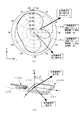
図19は、本実施形態に係るアンテナ装置における放射特性を示す図(シミュレーション結果)である。図19(a)は、本実施形態に係るアンテナ装置における放射特性を示す図であり、図19(b)は、本実施形態に係るアンテナ装置を備えた電子機器における円偏波の指向性を示す図である。
Next, the effect of improving the radiation characteristics in the present embodiment will be specifically described by showing the results of a simulation experiment.
FIG. 19 is a diagram (simulation result) showing radiation characteristics in the antenna device according to the present embodiment. FIG. 19A is a diagram showing the radiation characteristics of the antenna device according to the present embodiment, and FIG. 19B shows the directivity of circular polarization in the electronic apparatus including the antenna device according to the present embodiment. FIG.
本実施形態に係る電子機器において、GPSに適用される概ね1.57542GHz(1.6GHz)の周波数の電磁波を、直線偏波型のアンテナ素子を用いて放射するシミュレーション実験を行った結果、図19(a)に示すような放射パターンが得られた。 In the electronic device according to the present embodiment, as a result of conducting a simulation experiment in which an electromagnetic wave having a frequency of approximately 1.57542 GHz (1.6 GHz) applied to GPS is radiated using a linearly polarized antenna element, FIG. A radiation pattern as shown in (a) was obtained.
ここで、図19(b)に示す電子機器100Cを参照して説明すると、図19(a)は、機器本体101において、表示部111が設けられた一面(図面上面)を含むX−Y平面に直交するY−Z平面(腕時計の場合には図19(b)では6時−12時方向(Y軸)を通り、X−Y平面に直交する平面;シミュレーション実験の都合上、図10(a)に示した座標軸とは異なることに注意)における放射パターンを示す。すなわち、ここでは、機器本体101の上記一面の平面形状の中心を基準として、ベルト部102の延在方向(図19(b)の右方向;腕時計の場合には12時方向)をY軸方向と規定し、このY軸に直交する方向(図19(a)の手前方向;腕時計の場合には3時方向)をX軸方向と規定し、また、X−Y平面に直交する方向(図19(b)の上方向;腕時計の場合には手首と反対方向)をZ軸方向と規定した場合のY−Z平面(腕時計の場合には6時−12時方向(Y軸)を通り、X−Y平面に直交する平面)における放射パターンを示す。図19(a)において、放射パターンPRは、Y−Z平面内の全周方向(θ=0〜360°)における右旋偏波に対する放射成分であり、また、放射パターンPLは、Y−Z平面内の全周方向(θ=0〜360°)における左旋偏波に対する放射成分である。なお、このシミュレーション実験においては、上記のY−Z平面内における電磁波の位相が90°異なる(ずれる)ように、図18(a)、(b)及び図19(b)に示した導電性素子113gにおいて、導波器として機能する導電性パターンEPやインダクタンスとして機能する導電性パターンLP、キャパシタンスとして機能する導電性パターンEPとLPとの間の離間部分の、伝送路長や誘導線路、容量線路を設定した。
Here, with reference to the electronic device 100C shown in FIG. 19B, FIG. 19A shows an XY plane including one surface (upper surface in the drawing) on which the display unit 111 is provided in the device
このシミュレーション実験の結果によれば、図19(a)、(b)に示すように、右旋偏波の放射成分において、Z軸からY軸方向への回転角度θが概ね60°の方向に強い指向性を示すことが判明した。また、左旋偏波の放射成分においては、上記の回転角度θが概ね140°の方向に強い指向性を示すことが判明した。すなわち、導電性素子113gを構成する伝送路長や誘導線路、容量線路を、アンテナ素子112から放射される電磁波の位相差が90°に設定されるように適切に設計することにより、直線偏波用のチップアンテナで、良好な指向性を有する円偏波を発生させることができることが判明した。ここで、図19(b)に示すように、電子機器100Cを利用者が手首に装着し、表示部111を視認している状態で、右旋偏波が強い指向性を示す方向(θ=60°)が天空を向くように、本実施形態に係るアンテナ装置を設計することにより、簡易かつ小型の構成でGPS衛星から送信される電磁波(右旋偏波)を良好に受信することができる。なお、図11(a)に示したように、電子機器100Cを利用者が手首に装着し、表示部111を視認している状態では、右旋偏波が天空方向に強い指向性を示すのに対して、左旋偏波は概ね地表方向に強い指向性を示す。ここで、この左旋偏波はGPSには不要な円偏波であり、指向性を示す方向は人体方向になるため、GPSに適用するアンテナ装置の放射特性に影響を与えることはない。このように、本実施形態によれば、簡易かつ小型の構成で良好な放射特性を有するとともに、所望の円偏波に対応したアンテナ装置や指向性制御が可能なアンテナ装置を実現することができる。
According to the result of this simulation experiment, as shown in FIGS. 19A and 19B, the rotation angle θ from the Z-axis to the Y-axis direction is approximately 60 ° in the right-hand polarized radiation component. It turned out to show strong directivity. Further, it has been found that the left-handed polarized radiation component exhibits strong directivity in the direction in which the rotation angle θ is approximately 140 °. That is, by appropriately designing the transmission line length, the induction line, and the capacitive line constituting the
<第3の実施形態の変形例>
次に、上述した第3の実施形態の変形例について説明する。
図20は、第3の実施形態に係る電子機器に適用される導電性素子の変形例を示す概略構成図である。ここで、図20(a)は、本実施形態に係る導電性素子の概略構成を示す斜視図であり、図20(b)は、図20(a)に示した導電性素子におけるXXB−XXB線(本明細書においては図20中に示したローマ数字の「20」に対応する記号として便宜的に「XX」を用いる。)に沿った断面構造を示す概略図である。なお、図20(a)においても、図示を明瞭にするために、導電性素子に便宜的にハッチングを施して示した。
<Modification of Third Embodiment>
Next, a modification of the above-described third embodiment will be described.
FIG. 20 is a schematic configuration diagram illustrating a modified example of the conductive element applied to the electronic apparatus according to the third embodiment. Here, FIG. 20A is a perspective view showing a schematic configuration of the conductive element according to the present embodiment, and FIG. 20B is XXB-XXB in the conductive element shown in FIG. FIG. 21 is a schematic diagram showing a cross-sectional structure along a line (in this specification, “XX” is used as a symbol corresponding to the Roman numeral “20” shown in FIG. 20 for convenience). In FIG. 20 (a), the conductive elements are hatched for the sake of convenience for the sake of clarity.
上述した第1乃至第3の実施形態においては、電子機器100A〜100Cの筐体110や機器本体101の内部に設けられたアンテナ素子112に対向する領域に、特定の周波数の電磁波が伝搬される構成に対応した導電性素子113、113a〜113gを設けた構成を示した。本実施形態の変形例においては、複数の周波数の電磁波が伝搬される構成に対応した導電性素子を設けた構成を有している。ここで、このような導電性素子については、例えば特開2011−176495号公報に記載されているアンテナ装置の構成を良好に適用することができる。
In the first to third embodiments described above, an electromagnetic wave having a specific frequency is propagated to a region facing the
本実施形態に係る導電性素子の変形例は、例えば図20(a)、(b)に示すように、誘電体として機能する絶縁性基板SDと、当該絶縁性基板SDの一面側(図面上面側)に設けられた導電性パターンEP(EPa、EPb)、LPa、VPと、絶縁性基板SDの他面側(図面下面側)に設けられた導電性パターンLPb、CPと、導電性パターンEPと導電性パターンLPb、また、導電性パターンVPと導電性パターンCPを、それぞれ電気的に接続するビアVCa、VCbと、を備えた多層構造を有している。 For example, as shown in FIGS. 20A and 20B, a modification of the conductive element according to the present embodiment includes an insulating substrate SD functioning as a dielectric, and one surface side of the insulating substrate SD (upper surface in the drawing). Conductive patterns EP (EPa, EPb), LPa, VP provided on the side), conductive patterns LPb, CP provided on the other surface side (lower surface side of the drawing), and conductive pattern EP provided on the insulating substrate SD. And a conductive pattern LPb, and vias VCa and VCb that electrically connect the conductive pattern VP and the conductive pattern CP, respectively.
導電性パターンEPは、図20(a)に示すように、上底(図面右方側の辺)より下底(図面左方側の辺)が長い等脚台形の平面形状を有する導電性パターンEPaと、当該導電性パターンEPaの下底に接続された半円形の平面形状を有する導電性パターンEPbと、から構成されている。また、導電性パターンEPは、導電性パターンEPaの所定の位置において、絶縁性基板SDを厚さ方向に貫通するビアVCaを介して、絶縁性基板SDの他面側に設けられた導電性パターンLPbに電気的に接続されている。 As shown in FIG. 20A, the conductive pattern EP has a planar shape of an isosceles trapezoid whose lower base (side on the left side in the drawing) is longer than the upper base (side on the right side in the drawing). EPa and a conductive pattern EPb having a semicircular planar shape connected to the bottom of the conductive pattern EPa. In addition, the conductive pattern EP is a conductive pattern provided on the other surface side of the insulating substrate SD through a via VCa penetrating the insulating substrate SD in the thickness direction at a predetermined position of the conductive pattern EPa. It is electrically connected to LPb.
導電性パターンVPは、上記導電性パターンEPaの上底に対向するように配置され、絶縁性基板SDを厚さ方向に貫通するビアVCbを介して、絶縁性基板SDの他面側に設けられた導電性パターンCPに電気的に接続されている。また、導電性パターンLPaは、導電性パターンEPの延在方向(図面左右方向)に延在するように設けられ、一端側が上記導電性パターンVPに接続されている。 The conductive pattern VP is disposed so as to face the upper bottom of the conductive pattern EPa, and is provided on the other surface side of the insulating substrate SD via a via VCb penetrating the insulating substrate SD in the thickness direction. The conductive pattern CP is electrically connected. In addition, the conductive pattern LPa is provided so as to extend in the extending direction of the conductive pattern EP (the left-right direction in the drawing), and one end side is connected to the conductive pattern VP.
導電性パターンCPは、導電性パターンEPに対向し、当該導電性パターンEPの延在方向(図面左右方向)に延在する導電性パターンLPbを挟み込むように、一対設けられている。ここで、導電性パターンCPは、絶縁性基板SDを平面視した場合に、上記の導電性パターンEPと平面的に重なるように配置されている。 A pair of conductive patterns CP are provided so as to sandwich the conductive pattern LPb facing the conductive pattern EP and extending in the extending direction of the conductive pattern EP (the horizontal direction in the drawing). Here, the conductive pattern CP is arranged to overlap the conductive pattern EP in a plan view when the insulating substrate SD is viewed in plan.
このような構成を有する導電性素子113hにおいて、導電性パターンEPは、上述した第3の実施形態に示した導波器として機能し、導電性パターン(インダクタ用導電性部材)LPaは、上述した第3の実施形態に示したインダクタンス(誘導線路)として機能する。また、絶縁性基板SDを介して対向する導電性パターン(キャパシタ用導電性部材)EPと導電性パターン(キャパシタ用導電性部材)CPにより、上述した第3の実施形態に示したキャパシタンス(容量線路)が形成される。 In the conductive element 113h having such a configuration, the conductive pattern EP functions as the director shown in the above-described third embodiment, and the conductive pattern (inductive conductive member) LPa is described above. It functions as the inductance (induction line) shown in the third embodiment. Further, the capacitance (capacitor line) shown in the above-described third embodiment is formed by the conductive pattern (conductive member for capacitor) EP and the conductive pattern (conductive member for capacitor) CP facing each other through the insulating substrate SD. ) Is formed.
そして、導電性素子113hは、上述した第3の実施形態に示した場合と同様に、機器本体101に内蔵されたアンテナ素子112に対向するように、ベルト部102の任意の領域に設けられる。ここで、導電性素子113hは、絶縁性基板SDとしてベルト部102を構成する帯状(薄板状)の部材を適用して、当該ベルト部102の表面及び裏面に直接各導電性パターンを形成して、ビアを介して表面側と裏面側の導電性パターンを電気的に接続することにより、ベルト部102に一体的に組み込まれる。なお、導電性素子113hは、薄板状やフィルム状の絶縁性基板SDの両面に、上述した各導電性パターンを形成した構成を有することにより、図18(a)に示したように、ベルト部102の収納部102aに収納された状態で、カバー部材103により閉止してベルト部102の内部に組み込まれるものであってもよい。
The conductive element 113h is provided in an arbitrary region of the
このようなアンテナ装置において、導電性素子113hを構成する各導電性パターンの伝送路長や誘導線路、容量線路を適切に設計することにより、上述した特開2011−176495号公報に記載されているように、複数の共振周波数で動作するアンテナ装置を実現することができる。 In such an antenna device, it is described in Japanese Patent Application Laid-Open No. 2011-176495 described above by appropriately designing the transmission path length, induction line, and capacitance line of each conductive pattern constituting the conductive element 113h. Thus, an antenna device that operates at a plurality of resonance frequencies can be realized.
したがって、本実施形態に係るアンテナ装置を備えた電子機器によれば、導電性素子113hの設計自由度が高く、簡易かつ小型の構成で良好な放射特性を有するとともに、単一の導電性素子により複数周波数に対応した電磁波を放射することができるアンテナ装置を実現することができ、電子機器の高機能化に寄与することができる。 Therefore, according to the electronic apparatus including the antenna device according to the present embodiment, the conductive element 113h has a high degree of freedom in design, has a good radiation characteristic with a simple and small configuration, and has a single conductive element. An antenna device that can radiate electromagnetic waves corresponding to a plurality of frequencies can be realized, and can contribute to the enhancement of functions of electronic devices.
<アンテナ装置の適用例>
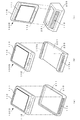
次に、本発明に係るアンテナ装置の適用例について説明する。
上述した第1の実施形態においては、電子機器100Aの筐体110の側面に導電性素子113、113a〜113eを設けた構成について説明し、また、第2及び第3の実施形態においては、腕時計型の電子機器100B、100Cの機器本体101に一体的に付設されたベルト部102に導電性素子113f〜113hを設けた構成について説明した。本発明に係るアンテナ装置は、上述した各実施形態に示した電子機器への適用例に限定されるものではなく、以下に説明するように、電子機器に対して着脱可能に取り付け固定される種々の製品や部品に導電性素子を設けた構成を適用することができる。ここで、この構成に適用される電子機器は、筐体や機器本体の内部にアンテナ素子が設けられた構成を有しているが、筐体や機器本体の側面や付設された部材には導電性素子が設けられていない。
<Application example of antenna device>
Next, application examples of the antenna device according to the present invention will be described.
In the first embodiment described above, a configuration in which the
図21、図22は、本発明に係るアンテナ装置を適用した電子機器の他の適用例を示す概略構成図である。なお、図21、図22においても、図示を明瞭にするために、導電性素子に便宜的にハッチングを施して示した。また、上述した実施形態と同等の構成については同一の符号を付して説明を簡略化する。 21 and 22 are schematic configuration diagrams illustrating other application examples of the electronic apparatus to which the antenna device according to the present invention is applied. 21 and 22 also show the conductive elements hatched for the sake of convenience for the sake of clarity. Further, the same components as those in the above-described embodiment are denoted by the same reference numerals, and the description is simplified.
本発明に係るアンテナ装置の第1の適用例は、例えば図21(a)に示すように、電子機器100Dの側面及び背面(図面下面側)を外部からの衝撃や水分等から保護するための保護カバー210に、導波器として機能する導電性素子113を設けた構成を有している。ここで、保護カバー(保持部材)210は、電子機器100Dを保護するために保護カバー210に取り付けた(凹部211に嵌め込み固定した)状態で、筐体110のアンテナ素子112に近接して対向する側面部分に導電性素子113が配置された構成を有している。なお、保護カバー210に設けられる導電性素子113は、上述した第1の実施形態に示した場合(図8、図9参照)と同様に、アンテナ素子112に近接して対向する保護カバー210の側面部分を含む複数の側面部分に、個別に設けられるものであってもよいし、連続して一体的に設けられるものであってもよい。
The first application example of the antenna device according to the present invention is, for example, as shown in FIG. 21A, for protecting the side surface and the back surface (the lower surface side of the drawing) of the
また、本発明に係るアンテナ装置の第2の適用例は、例えば図21(b)に示すように、電子機器100Dの内蔵バッテリー(図示を省略)を充電するための充電用ホルダー(ホルダー型充電器;保持部材)220に、導波器として機能する導電性素子113a、113bを設けた構成を有している。ここで、充電用ホルダー220は、電子機器100Dを搭載部221に挟持固定した状態で、筐体110のアンテナ素子112に近接して対向する領域、及び、電子機器100Dを挟んでそれに対向する領域に、それぞれ導電性素子113a、113bが配置された構成を有している。なお、充電用ホルダー220に設けられる導電性素子113a、113bは、上述した第1の適用例と同様に、アンテナ素子112に近接して対向する充電用ホルダー220の任意の領域を含む複数の領域に、個別に設けられるものであってもよいし、連続して一体的に設けられるものであってもよい。
Further, a second application example of the antenna device according to the present invention is, for example, as shown in FIG. 21B, a charging holder (holder-type charging) for charging a built-in battery (not shown) of the
また、本発明に係るアンテナ装置の第3の適用例は、例えば図21(c)に示すように、電子機器100Dの内蔵バッテリー(図示を省略)を充電するための充電用スタンド(スタンド型充電器;保持部材)230に、導波器として機能する導電性素子113を設けた構成を有している。ここで、充電用スタンド230は、電子機器100Dを嵌合部231に挿入固定した状態で、筐体110のアンテナ素子112に近接して対向する領域に導電性素子113が配置された構成を有している。なお、充電用スタンド230に設けられる導電性素子113は、上述した第1及び第2の適用例と同様に、アンテナ素子112に近接して対向する充電用スタンド230の任意の領域を含む複数の領域に、個別に設けられるものであってもよいし、連続して一体的に設けられるものであってもよい。
Further, a third application example of the antenna device according to the present invention is, for example, as shown in FIG. 21C, a charging stand (stand-type charging) for charging a built-in battery (not shown) of the
なお、上述した第1乃至第3の適用例においては、アンテナ素子112が筐体110の特定の側面(図21手前側の側面)に近接する位置に配置された構成を有する電子機器100Dに、本発明に係るアンテナ装置を適用する場合について説明したが、本発明はこれに限定されるものではない。すなわち、筐体110の背面側に金属製の裏蓋等の導電性の部材が用いられていない電子機器においては、筐体110の背面側近傍にアンテナ素子を設けることができる。このような構成を有する電子機器の場合には、例えば図22(a)に示すように、保護カバー210は、電子機器100Eを保護カバー210に取り付けた状態で、筐体110のアンテナ素子112に近接して対向する、凹部211の底面の任意の領域に導電性素子113が配置された構成を有しているものであってもよい。また、例えば図22(b)に示すように、充電用ホルダー220は、電子機器100Eを搭載部221に挟持固定した状態で、筐体110のアンテナ素子112に近接して対向する、搭載部221の任意の領域に導電性素子113が配置された構成を有しているものであってもよい。また、例えば図22(c)に示すように、充電用スタンド230は、電子機器100Eを嵌合部231に挿入固定した状態で、筐体110のアンテナ素子112に近接して対向する、背面支持部の任意の領域に導電性素子113が配置された構成を有しているものであってもよい。
Note that in the first to third application examples described above, the
このような構成を有するアンテナ装置を適用した電子機器100Eによれば、保護カバー210を取り付け固定した状態や、充電用ホルダー220や充電用スタンド230に取り付け固定した状態で、上述した実施形態と同様に、電磁波の放射特性(アンテナ特性)を向上させることができる。また、電子機器100Eの筐体110に着脱可能に取り付け固定される保護カバー210や、充電用ホルダー220、充電用スタンド230等の周辺製品や部品に、導電性素子113を設けた構成を適用することができるので、電子機器100Eの筐体110の外面に導電性素子を設ける必要がなく、筐体やベルト部に導電性素子が設けられていない既存の電子機器をそのまま適用することができるとともに、導電性素子の設計自由度を高めることができる。また、筐体110に取り付けられる多様な周辺製品や部品に、本発明に係るアンテナ装置の構成を組み込むことができるので、導電性素子の設計自由度電子機器の利便性を高めつつ、簡易な構成で電磁波の放射特性を向上させることができる。
According to the electronic device 100E to which the antenna device having such a configuration is applied, the
以上、本発明のいくつかの実施形態について説明したが、本発明は、上述した実施形態に限定されるものではなく、特許請求の範囲に記載された発明とその均等の範囲を含むものである。
以下に、本願出願の当初の特許請求の範囲に記載された発明を付記する。
As mentioned above, although some embodiment of this invention was described, this invention is not limited to embodiment mentioned above, It includes the invention described in the claim, and its equivalent range.
Hereinafter, the invention described in the scope of claims of the present application will be appended.
(付記)
[1]
少なくとも一つの特定の周波数の第1の電磁波を送信又は受信するアンテナ素子と、
前記アンテナ素子と離間して前記アンテナ素子に対向して配置され、前記第1の電磁波に対して共振して、前記特定の周波数の第2の電磁波を送信又は受信する、導電性を有する材料により形成された導電性素子と、
を備え、
前記導電性素子は、前記特定の周波数で共振する形状と大きさを有していることを特徴とするアンテナ装置である。
(Appendix)
[1]
An antenna element for transmitting or receiving at least one first electromagnetic wave of a specific frequency;
A conductive material that is disposed away from the antenna element and faces the antenna element, resonates with the first electromagnetic wave, and transmits or receives the second electromagnetic wave with the specific frequency. Formed conductive elements;
With
The conductive element is an antenna device characterized by having a shape and size that resonates at the specific frequency.
[2]
内部に密閉された空間を有する筐体と、前記筐体を人体に装着するためのバンド部材と、を有し、
前記アンテナ素子は、前記筐体の内部に設けられ、
前記導電性素子は、少なくとも、前記バンド部材内、前記筐体の前記アンテナ素子に対向する位置における前記筐体の外面又は前記筐体を構成する部材内、又は、前記筐体を保持する保持部材内、の何れかに埋め込まれて設けられ、
前記筐体の、前記アンテナ素子に対向する領域の部材が、絶縁性を有する材料により形成されていることを特徴とする[1]に記載のアンテナ装置である。
[2]
A housing having a sealed space inside, and a band member for mounting the housing on a human body,
The antenna element is provided inside the housing,
The conductive element is at least in the band member, in an outer surface of the casing at a position facing the antenna element of the casing or in a member constituting the casing, or a holding member for holding the casing Embedded in any of the above,
The antenna device according to [1], wherein a member of a region of the casing facing the antenna element is formed of an insulating material.
[3]
前記導電性素子は、前記バンド部材内に埋め込まれて設けられ、
前記バンド部材の、前記導電性素子に接している領域の部材が、絶縁性を有する部材により形成され、
前記導電性素子は、直線状の第1の辺と第2の辺とを有し、前記第1の辺及び前記第2の辺の長さは前記特定の周波数の波長の1/2n(n=0、1、2、3、・・)の長さに設定され、前記第1の辺と前記第2の辺とが互いに交差する方向に延在して屈曲した形状を有していることを特徴とする[2]に記載のアンテナ装置である。
[3]
The conductive element is provided embedded in the band member,
A member of a region of the band member that is in contact with the conductive element is formed of an insulating member,
The conductive element has a linear first side and a second side, and the lengths of the first side and the second side are ½ n of the wavelength of the specific frequency ( n = 0, 1, 2, 3,...), and the first side and the second side have a bent shape extending in a direction intersecting each other. This is an antenna device according to [2].
[4]
前記導電性素子は、インダクタンスを形成するインダクタ用導電性部材と、キャパシタンスを形成するキャパシタ用導電性部材とを有して、前記特定の周波教で共振する共振回路をなしていることを特徴とする[3]に記載のアンテナ装置である。
[4]
The conductive element includes an inductor conductive member that forms an inductance and a capacitor conductive member that forms a capacitance, and forms a resonance circuit that resonates at the specific frequency. The antenna device according to [3].
[5]
前記共振回路は、複数の互いに異なる前記特定の周波教で共振する特性を有していることを特徴とする[4]に記載のアンテナ装置である。
[5]
The antenna device according to [4], wherein the resonance circuit has a characteristic of resonating at a plurality of different specific frequencies.
[6]
前記導電性素子は、前記筐体の前記アンテナ素子に対向する位置を含む、前記筐体の外面又は前記筐体を構成する部材内に埋め込まれて設けられ、
前記筐体の、前記導電性素子に接している領域の部材が、絶縁性を有する材料により形成され、
前記導電性素子は、直線状の第1の辺を有し、前記第1の辺の長さは前記特定の周波数の波長の1/2n(n=0、1、2、3、・・)の長さに設定されていることを特徴とする[2]に記載のアンテナ装置である。
[6]
The conductive element is embedded in a member constituting the outer surface of the casing or the member including the position including the position facing the antenna element of the casing,
The member of the region in contact with the conductive element of the housing is formed of an insulating material,
The conductive element has a linear first side, and the length of the first side is 1/2 n (n = 0, 1, 2, 3,...) Of the wavelength of the specific frequency. The antenna device according to [2], wherein the antenna device is set to a length of
[7]
前記導電性素子は、少なくとも一つの導電性部材を有して形成され、
前記導電性部材は前記筐体の周囲の、互いに交差する方向に延在する複数の面に跨って設けられていることを特徴とする[6]に記載のアンテナ装置である。
[7]
The conductive element is formed having at least one conductive member,
The antenna device according to [6], wherein the conductive member is provided across a plurality of surfaces extending in a direction intersecting each other around the casing.
[8]
前記複数の面の各々に設けられている前記導電性部材は、互いに分離されていることを特徴とする[7]に記載のアンテナ装置である。
[8]
The antenna device according to [7], wherein the conductive members provided on each of the plurality of surfaces are separated from each other.
[9]
前記導電性素子は、前記保持部材における、前記筐体が保持された状態で前記アンテナ素子に対向する位置に設けられ、
前記保持部材の、前記導電性素子に接している領域の部材が、絶縁性を有する材料により形成され、
前記導電性素子は、直線状の第1の辺を有し、前記第1の辺の長さは前記特定の周波数の波長の1/2n(n=0、1、2、3、・・)の長さに設定されていることを特徴とする[2]に記載のアンテナ装置である。
[9]
The conductive element is provided at a position facing the antenna element in the state where the housing is held in the holding member,
A member in a region of the holding member that is in contact with the conductive element is formed of an insulating material,
The conductive element has a linear first side, and the length of the first side is 1/2 n (n = 0, 1, 2, 3,...) Of the wavelength of the specific frequency. The antenna device according to [2], wherein the antenna device is set to a length of
[10]
電子機器本体部と、
前記[1]に記載のアンテナ装置と、
を備え、
前記アンテナ装置に前記電子機器本体部から信号が供給されていることを特徴とする電子機器である。
[10]
An electronic device body,
The antenna device according to [1],
With
In the electronic device, a signal is supplied to the antenna device from the electronic device main body.
[11]
内部に密閉された空間を有する筐体と、前記筐体を人体に装着するためのバンド部材と、を有し、
前記電子機器本体部及び前記アンテナ素子は、前記筐体の内部に設けられ、
前記導電性素子は、少なくとも、前記バンド部材内、前記筐体の前記アンテナ素子に対向する位置における前記筐体の外面又は前記筐体を構成する部材内、又は、前記筐体を保持する保持部材内、の何れかに埋め込まれて設けられ、
前記筐体の、前記アンテナ素子に対向する領域の部材が、絶縁性を有する材料により形成されていることを特徴とする[10]に記載の電子機器である。
[11]
A housing having a sealed space inside, and a band member for mounting the housing on a human body,
The electronic device main body and the antenna element are provided inside the housing,
The conductive element is at least in the band member, in an outer surface of the casing at a position facing the antenna element of the casing or in a member constituting the casing, or a holding member for holding the casing Embedded in any of the above,
[10] The electronic device according to [10], wherein a member in a region of the housing facing the antenna element is formed of an insulating material.
100A〜100E 電子機器
101 機器本体
102 ベルト部
110 筐体
111 表示部
112 アンテナ素子
113、113a〜113h 導電性素子
210 保護カバー
220 充電用ホルダー
230 充電用スタンド
EP 導電性パターン
LP 導電性パターン
CP 導電性パターン
100A to
Claims (10)
前記アンテナ素子と離間して前記アンテナ素子に対向して配置され、導電性を有する材料により形成され、無給電素子をなす導電性素子と、
内部に密閉された空間を有する筐体と、
を備え、
前記アンテナ素子は、前記筐体の内部に設けられており、
前記導電性素子は、
前記筐体に取り付けられたバンド部材内に設けられ、
前記アンテナ素子と電磁界結合して、前記特定の周波数に対して共振して、前記電磁波を送信又は受信し、
前記バンド部材の、前記導電性素子に接している領域の部材は、絶縁性を有する部材により形成され、
前記導電性素子は、
直線状の第1の辺と直線状の第2の辺とを有し、
前記第1の辺及び前記第2の辺は、それぞれ前記特定の周波数の波長の1/2 n (n=0、1、2、3、・・)の長さを有し、
前記導電性素子は、前記第1の辺と前記第2の辺とが互いに交差する方向に延在して、屈曲した形状を有していることを特徴とするアンテナ装置。 An antenna element for transmitting or receiving electromagnetic waves of at least one specific frequency;
A conductive element disposed away from the antenna element and facing the antenna element, formed of a conductive material, and forming a parasitic element;
A housing having a sealed space inside,
With
The antenna element is provided inside the housing,
The conductive element is
Provided in-band member attached to the housing,
Said antenna elements and electromagnetically coupling said resonating to a particular frequency, transmitting or receiving the electromagnetic wave,
A member of the band member that is in contact with the conductive element is formed of an insulating member,
The conductive element is
A linear first side and a linear second side;
Each of the first side and the second side has a length of 1/2 n (n = 0, 1, 2, 3,...) Of the wavelength of the specific frequency ,
The conductive elements may extend in a direction of the first side and said second side intersect with each other, the antenna apparatus characterized that you have have a bent shape.
前記導電性素子は、前記バンド部材における、前記筐体が保持された状態で前記アンテナ素子に対向する位置に設けられ、
前記バンド部材の、前記導電性素子に接している領域の部材が、絶縁性を有する材料により形成され、
前記導電性素子は、直線状の第3の辺を有し、前記第3の辺の長さは前記特定の周波数の波長の1/2n(n=0、1、2、3、・・)の長さに設定されていることを特徴とする請求項2に記載のアンテナ装置。 The conductive element is provided in the band member ,
The conductive element is provided in the band member at a position facing the antenna element in a state where the housing is held,
A member of the band member that is in contact with the conductive element is formed of an insulating material,
The conductive element has a straight third side, and the length of the third side is 1/2 n (n = 0, 1, 2, 3,...) Of the wavelength of the specific frequency. The antenna device according to claim 2, wherein the antenna device is set to a length of
前記請求項1に記載のアンテナ装置と、
を備え、
前記アンテナ装置に前記電子機器本体部から信号が供給されていることを特徴とする電子機器。 An electronic device main body having a communication control function for controlling communication with an external device;
The antenna device according to claim 1;
With
An electronic device, wherein a signal is supplied to the antenna device from the electronic device main body.
前記アンテナ素子と離間して前記アンテナ素子に対向して配置され、導電性を有する材料により形成され、無給電素子をなす導電性素子と、A conductive element disposed away from the antenna element and facing the antenna element, formed of a conductive material, and forming a parasitic element;
内部に密閉された空間を有する筐体と、A housing having a sealed space inside,
を備え、With
前記アンテナ素子は、前記筐体の内部に設けられており、The antenna element is provided inside the housing,
前記導電性素子は、The conductive element is
前記筐体の外面又は前記筐体を構成する部材内の、前記アンテナ素子に対向する位置に設けられ、Provided at a position facing the antenna element in the outer surface of the casing or a member constituting the casing,
前記アンテナ素子と電磁界結合して、前記特定の周波数に対して共振して、前記電磁波を送信又は受信し、Electromagnetic field coupling with the antenna element, resonating with respect to the specific frequency, transmitting or receiving the electromagnetic wave,
前記筐体の、前記導電性素子に接している領域の部材は、絶縁性を有する材料により形成され、The member of the region in contact with the conductive element of the housing is formed of an insulating material,
前記導電性素子は、直線状の第1の辺を有し、The conductive element has a linear first side;
前記第1の辺の長さは前記特定の周波数の波長の1/2The length of the first side is 1/2 of the wavelength of the specific frequency. nn (n=0、1、2、3、・・)の長さに設定されていることを特徴とするアンテナ装置。An antenna device characterized in that the length is set to (n = 0, 1, 2, 3, ...).
前記導電性部材は前記筐体の周囲の、互いに交差する方向に延在する複数の面に設けられていることを特徴とする請求項8に記載のアンテナ装置。The antenna device according to claim 8, wherein the conductive member is provided on a plurality of surfaces extending in a direction crossing each other around the casing.
Priority Applications (4)
| Application Number | Priority Date | Filing Date | Title |
|---|---|---|---|
| JP2013059429A JP5907479B2 (en) | 2013-03-22 | 2013-03-22 | ANTENNA DEVICE AND ELECTRONIC DEVICE |
| US14/222,504 US9680204B2 (en) | 2013-03-22 | 2014-03-21 | Antenna device |
| CN201410108236.7A CN104064854B (en) | 2013-03-22 | 2014-03-21 | Antenna assembly and electronic equipment |
| US15/498,959 US20170229764A1 (en) | 2013-03-22 | 2017-04-27 | Antenna device |
Applications Claiming Priority (1)
| Application Number | Priority Date | Filing Date | Title |
|---|---|---|---|
| JP2013059429A JP5907479B2 (en) | 2013-03-22 | 2013-03-22 | ANTENNA DEVICE AND ELECTRONIC DEVICE |
Related Child Applications (1)
| Application Number | Title | Priority Date | Filing Date |
|---|---|---|---|
| JP2016011981A Division JP6119883B2 (en) | 2016-01-26 | 2016-01-26 | Antenna device |
Publications (3)
| Publication Number | Publication Date |
|---|---|
| JP2014187452A JP2014187452A (en) | 2014-10-02 |
| JP2014187452A5 JP2014187452A5 (en) | 2015-04-09 |
| JP5907479B2 true JP5907479B2 (en) | 2016-04-26 |
Family
ID=51552453
Family Applications (1)
| Application Number | Title | Priority Date | Filing Date |
|---|---|---|---|
| JP2013059429A Active JP5907479B2 (en) | 2013-03-22 | 2013-03-22 | ANTENNA DEVICE AND ELECTRONIC DEVICE |
Country Status (3)
| Country | Link |
|---|---|
| US (2) | US9680204B2 (en) |
| JP (1) | JP5907479B2 (en) |
| CN (1) | CN104064854B (en) |
Families Citing this family (21)
| Publication number | Priority date | Publication date | Assignee | Title |
|---|---|---|---|---|
| JP6496939B2 (en) * | 2014-07-07 | 2019-04-10 | ソニー株式会社 | Mounting table, communication device, antenna characteristic correction member, and communication system |
| KR102305975B1 (en) | 2014-10-22 | 2021-09-28 | 삼성전자주식회사 | Antenna apparatus for use in wireless devices |
| TW201619755A (en) * | 2014-11-28 | 2016-06-01 | 廣達電腦股份有限公司 | Wearable device |
| CN106605335B (en) * | 2014-12-08 | 2020-03-31 | 松下知识产权经营株式会社 | Antenna and electric device |
| KR102352448B1 (en) * | 2015-08-12 | 2022-01-18 | 삼성전자주식회사 | An electronic device including an antenna apparatus |
| JP6611165B2 (en) * | 2015-09-25 | 2019-11-27 | Fdk株式会社 | Antenna device |
| US9948006B2 (en) * | 2015-12-22 | 2018-04-17 | Cheng Uei Precision Industry Co., Ltd. | Antenna assembly and electronic device including the same |
| US10709955B2 (en) * | 2016-03-15 | 2020-07-14 | Nike, Inc. | Athletic data aggregation for online communities |
| US10431878B2 (en) * | 2016-06-23 | 2019-10-01 | Verizon Patent And Licensing Inc. | Wearable device design for 4G antennas |
| TWI629832B (en) * | 2016-06-30 | 2018-07-11 | 和碩聯合科技股份有限公司 | Wearable electronic device |
| CN109845116A (en) * | 2016-10-24 | 2019-06-04 | 日本精机株式会社 | Portable communication appts |
| KR20180058016A (en) * | 2016-11-23 | 2018-05-31 | 삼성전자주식회사 | Antenna apparatus and electronic device including the same |
| US20180151949A1 (en) * | 2016-11-30 | 2018-05-31 | Trw Automotive Us Llc | Antenna with parasitic element |
| US10461402B2 (en) * | 2017-02-08 | 2019-10-29 | Intel Corporation | Mobile device with antenna-boosting case coupling |
| WO2018229973A1 (en) * | 2017-06-16 | 2018-12-20 | ヤマハ株式会社 | Wireless communication device |
| JP7039313B2 (en) * | 2018-02-14 | 2022-03-22 | オムロン株式会社 | Wireless communication devices, sensor devices and wearable devices |
| GB2571279B (en) * | 2018-02-21 | 2022-03-09 | Pet Tech Limited | Antenna arrangement and associated method |
| DE102018109671A1 (en) * | 2018-04-23 | 2019-10-24 | HELLA GmbH & Co. KGaA | Radio key with a loop antenna |
| CN109088144B (en) * | 2018-08-23 | 2021-01-05 | 北京小米移动软件有限公司 | Antenna of mobile terminal and mobile terminal |
| JP7230408B2 (en) * | 2018-10-02 | 2023-03-01 | カシオ計算機株式会社 | Antenna device and wristwatch type electronic device |
| CN110676557B (en) * | 2019-09-23 | 2021-09-10 | Oppo广东移动通信有限公司 | Electronic device |
Family Cites Families (43)
| Publication number | Priority date | Publication date | Assignee | Title |
|---|---|---|---|---|
| US4419770A (en) * | 1981-05-02 | 1983-12-06 | Sony Corporation | Wrist AM radio receiver |
| US4769656A (en) * | 1987-01-28 | 1988-09-06 | Timex Corporation | Expansion band antenna for a wrist instrument and method of making it |
| CH672870B5 (en) * | 1988-04-26 | 1990-07-13 | Ebauchesfabrik Eta Ag | |
| US4922260A (en) * | 1989-01-18 | 1990-05-01 | At & E Corporation | Adjustable watchband with embedded antenna |
| US5742256A (en) * | 1993-05-07 | 1998-04-21 | Seiko Epson Corporation | Wristband having embedded electrically conductive members for a wrist-mountable type electronic device |
| US5564082A (en) * | 1994-05-06 | 1996-10-08 | At&T Corp. | Diversity antenna for a wrist telephone |
| US5886669A (en) * | 1995-05-10 | 1999-03-23 | Casio Computer Co., Ltd. | Antenna for use with a portable radio apparatus |
| JP3639966B2 (en) * | 1995-07-20 | 2005-04-20 | カシオ計算機株式会社 | Antenna for portable radio equipment |
| JPH09307329A (en) * | 1996-05-14 | 1997-11-28 | Casio Comput Co Ltd | Antenna, its manufacture and electronic device or electric watch provided with the antenna |
| JP2001077611A (en) * | 1999-09-06 | 2001-03-23 | Tdk Corp | Movable object communication machine |
| US20010050643A1 (en) * | 2000-02-22 | 2001-12-13 | Igor Egorov | Small-size broad-band printed antenna with parasitic element |
| JP2003037413A (en) * | 2001-07-25 | 2003-02-07 | Matsushita Electric Ind Co Ltd | Antenna for portable wireless device |
| US6963595B2 (en) * | 2001-08-29 | 2005-11-08 | Cymer, Inc. | Automatic gas control system for a gas discharge laser |
| JP3608735B2 (en) * | 2002-02-15 | 2005-01-12 | 松下電器産業株式会社 | ANTENNA DEVICE AND PORTABLE RADIO DEVICE |
| US7457650B2 (en) * | 2002-07-31 | 2008-11-25 | Matsushita Electric Industrial Co., Ltd. | Portable radio communication apparatus provided with boom portion with through hole |
| EP1445821A1 (en) * | 2003-02-06 | 2004-08-11 | Matsushita Electric Industrial Co., Ltd. | Portable radio communication apparatus provided with a boom portion |
| US20040222930A1 (en) * | 2003-05-07 | 2004-11-11 | Huei-Hsin Sun | Wrist antenna |
| US7034768B2 (en) * | 2003-09-24 | 2006-04-25 | Gas Technology Institute | Antenna system |
| WO2005096437A1 (en) * | 2004-04-02 | 2005-10-13 | Matsushita Electric Industrial Co., Ltd. | Portable wireless unit |
| JP3964401B2 (en) * | 2004-04-27 | 2007-08-22 | Necトーキン株式会社 | Antenna core, coil antenna, watch, mobile phone, electronic device |
| JP4063833B2 (en) * | 2004-06-14 | 2008-03-19 | Necアクセステクニカ株式会社 | Antenna device and portable radio terminal |
| US7038634B2 (en) * | 2004-07-02 | 2006-05-02 | Eta Sa Manufacture Horlogère Suisse | Optimization of a loop antenna geometry embedded in a wristband portion of a watch |
| JP2006191437A (en) * | 2005-01-07 | 2006-07-20 | Matsushita Electric Ind Co Ltd | Mobile wireless apparatus |
| FR2882163B1 (en) * | 2005-02-15 | 2011-05-27 | Thales Sa | AUTOMATIC DRIVING EQUIPMENT FOR ROTARY TURNING AIRCRAFT |
| JP4718882B2 (en) * | 2005-04-08 | 2011-07-06 | 株式会社日立製作所 | Sensor node |
| US20070109208A1 (en) * | 2005-11-16 | 2007-05-17 | Microsoft Corporation | Antenna in a shielded enclosure |
| US7463205B2 (en) * | 2005-12-22 | 2008-12-09 | Microsoft Corporation | Dipole antenna for a watchband |
| US8677515B2 (en) * | 2006-02-22 | 2014-03-25 | Nike, Inc. | Article of apparel incorporating a covered electronic device |
| US7215600B1 (en) * | 2006-09-12 | 2007-05-08 | Timex Group B.V. | Antenna arrangement for an electronic device and an electronic device including same |
| JP2008172672A (en) * | 2007-01-15 | 2008-07-24 | Matsushita Electric Ind Co Ltd | Antenna |
| CN101800354B (en) * | 2008-11-06 | 2015-03-11 | 庞研究有限公司 | Antenna embedded in battery, wireless device and intelligent housing of wireless device |
| US8957813B2 (en) * | 2009-03-13 | 2015-02-17 | Pong Research Corporation | External case for redistribution of RF radiation away from wireless communication device user and wireless communication device incorporating RF radiation redistribution elements |
| KR101622606B1 (en) * | 2009-07-15 | 2016-05-20 | 엘지전자 주식회사 | Watch type portable terminal |
| JP5050021B2 (en) * | 2009-09-11 | 2012-10-17 | 東芝テック株式会社 | Antenna device |
| JP4916036B2 (en) | 2010-02-23 | 2012-04-11 | カシオ計算機株式会社 | Multi-frequency antenna |
| JP5313955B2 (en) | 2010-03-26 | 2013-10-09 | シチズンホールディングス株式会社 | Radio wave watch |
| US8698677B2 (en) * | 2010-04-09 | 2014-04-15 | Sony Corporation | Mobile wireless terminal and antenna device |
| US8593351B2 (en) * | 2010-08-12 | 2013-11-26 | Mediatek Inc. | Portable electronic device |
| US9571612B2 (en) * | 2010-11-12 | 2017-02-14 | venyard GmbH | Wrist phone with improved voice quality |
| TW201304272A (en) * | 2011-07-15 | 2013-01-16 | Wistron Neweb Corp | Antenna structure for wearable electronic device and wearable wireless electronic device |
| JP5263365B2 (en) * | 2011-10-12 | 2013-08-14 | カシオ計算機株式会社 | Multi-frequency circularly polarized antenna |
| US9293816B2 (en) * | 2012-07-06 | 2016-03-22 | Apple Inc. | Electronic device plate antenna |
| WO2014107158A1 (en) * | 2013-01-04 | 2014-07-10 | Evado Filip Holding Ltd. | Band with an antenna for use with a wireless electronic device |
-
2013
- 2013-03-22 JP JP2013059429A patent/JP5907479B2/en active Active
-
2014
- 2014-03-21 US US14/222,504 patent/US9680204B2/en active Active
- 2014-03-21 CN CN201410108236.7A patent/CN104064854B/en active Active
-
2017
- 2017-04-27 US US15/498,959 patent/US20170229764A1/en not_active Abandoned
Also Published As
| Publication number | Publication date |
|---|---|
| US9680204B2 (en) | 2017-06-13 |
| US20140285385A1 (en) | 2014-09-25 |
| CN104064854A (en) | 2014-09-24 |
| CN104064854B (en) | 2017-06-27 |
| JP2014187452A (en) | 2014-10-02 |
| US20170229764A1 (en) | 2017-08-10 |
Similar Documents
| Publication | Publication Date | Title |
|---|---|---|
| JP5907479B2 (en) | ANTENNA DEVICE AND ELECTRONIC DEVICE | |
| US20210066803A1 (en) | Thin chassis near field communication (nfc) antenna integration | |
| KR101658766B1 (en) | Multipurpose antenna | |
| TWI790344B (en) | Slot mode antennas | |
| EP2883279B1 (en) | Multi layer 3d antenna carrier arrangement for electronic devices | |
| US9450297B2 (en) | Antenna for device having conducting casing | |
| TW201438337A (en) | Coupled antenna structure and methods | |
| JP6119883B2 (en) | Antenna device | |
| US20130241792A1 (en) | Antenna device, electronic apparatus, and wireless communication method | |
| JP2009021932A (en) | Electronic equipment, and manufacturing method thereof | |
| JP6891878B2 (en) | antenna | |
| TW201935770A (en) | Slot mode antennas | |
| KR20140093548A (en) | Microstrip chip antenna with top loading structure | |
| JP6222524B2 (en) | ANTENNA DEVICE AND ELECTRONIC DEVICE | |
| JP2005354501A (en) | Mobile radio terminal | |
| JP6414786B2 (en) | Mobile communication terminal and housing cover | |
| US9521222B1 (en) | Mobile communication device | |
| TWI518999B (en) | Open-loop type gps antenna | |
| WO2016152662A1 (en) | Antenna apparatus and electronic device | |
| JP2008187447A (en) | Antenna and component of antenna | |
| CN116780193A (en) | Wearable equipment | |
| TW201935763A (en) | Antenna assembly for customizable devices | |
| JP6345529B2 (en) | Antenna device for ultra-wideband communication | |
| KR20120134254A (en) | Dual planar inverted f antenna using electromagnetic coupling | |
| WO2010107137A1 (en) | Chip antenna |
Legal Events
| Date | Code | Title | Description |
|---|---|---|---|
| A521 | Written amendment |
Free format text: JAPANESE INTERMEDIATE CODE: A523 Effective date: 20150224 |
|
| A621 | Written request for application examination |
Free format text: JAPANESE INTERMEDIATE CODE: A621 Effective date: 20150224 |
|
| A977 | Report on retrieval |
Free format text: JAPANESE INTERMEDIATE CODE: A971007 Effective date: 20150604 |
|
| A131 | Notification of reasons for refusal |
Free format text: JAPANESE INTERMEDIATE CODE: A131 Effective date: 20150618 |
|
| A521 | Written amendment |
Free format text: JAPANESE INTERMEDIATE CODE: A523 Effective date: 20150807 |
|
| A131 | Notification of reasons for refusal |
Free format text: JAPANESE INTERMEDIATE CODE: A131 Effective date: 20160107 |
|
| A521 | Written amendment |
Free format text: JAPANESE INTERMEDIATE CODE: A523 Effective date: 20160126 |
|
| TRDD | Decision of grant or rejection written | ||
| A01 | Written decision to grant a patent or to grant a registration (utility model) |
Free format text: JAPANESE INTERMEDIATE CODE: A01 Effective date: 20160229 |
|
| R150 | Certificate of patent or registration of utility model |
Ref document number: 5907479 Country of ref document: JP Free format text: JAPANESE INTERMEDIATE CODE: R150 |
|
| A61 | First payment of annual fees (during grant procedure) |
Free format text: JAPANESE INTERMEDIATE CODE: A61 Effective date: 20160313 |