JP5898657B2 - Nonvolatile semiconductor memory device - Google Patents
Nonvolatile semiconductor memory device Download PDFInfo
- Publication number
- JP5898657B2 JP5898657B2 JP2013180932A JP2013180932A JP5898657B2 JP 5898657 B2 JP5898657 B2 JP 5898657B2 JP 2013180932 A JP2013180932 A JP 2013180932A JP 2013180932 A JP2013180932 A JP 2013180932A JP 5898657 B2 JP5898657 B2 JP 5898657B2
- Authority
- JP
- Japan
- Prior art keywords
- source line
- memory
- monitor position
- voltage
- source
- Prior art date
- Legal status (The legal status is an assumption and is not a legal conclusion. Google has not performed a legal analysis and makes no representation as to the accuracy of the status listed.)
- Expired - Fee Related
Links
Images


Classifications
-
- G—PHYSICS
- G11—INFORMATION STORAGE
- G11C—STATIC STORES
- G11C16/00—Erasable programmable read-only memories
- G11C16/02—Erasable programmable read-only memories electrically programmable
- G11C16/06—Auxiliary circuits, e.g. for writing into memory
- G11C16/26—Sensing or reading circuits; Data output circuits
-
- G—PHYSICS
- G11—INFORMATION STORAGE
- G11C—STATIC STORES
- G11C16/00—Erasable programmable read-only memories
- G11C16/02—Erasable programmable read-only memories electrically programmable
- G11C16/04—Erasable programmable read-only memories electrically programmable using variable threshold transistors, e.g. FAMOS
- G11C16/0483—Erasable programmable read-only memories electrically programmable using variable threshold transistors, e.g. FAMOS comprising cells having several storage transistors connected in series
-
- G—PHYSICS
- G11—INFORMATION STORAGE
- G11C—STATIC STORES
- G11C16/00—Erasable programmable read-only memories
- G11C16/02—Erasable programmable read-only memories electrically programmable
- G11C16/06—Auxiliary circuits, e.g. for writing into memory
- G11C16/34—Determination of programming status, e.g. threshold voltage, overprogramming or underprogramming, retention
- G11C16/3418—Disturbance prevention or evaluation; Refreshing of disturbed memory data
-
- H—ELECTRICITY
- H10—SEMICONDUCTOR DEVICES; ELECTRIC SOLID-STATE DEVICES NOT OTHERWISE PROVIDED FOR
- H10B—ELECTRONIC MEMORY DEVICES
- H10B43/00—EEPROM devices comprising charge-trapping gate insulators
- H10B43/20—EEPROM devices comprising charge-trapping gate insulators characterised by three-dimensional arrangements, e.g. with cells on different height levels
- H10B43/23—EEPROM devices comprising charge-trapping gate insulators characterised by three-dimensional arrangements, e.g. with cells on different height levels with source and drain on different levels, e.g. with sloping channels
- H10B43/27—EEPROM devices comprising charge-trapping gate insulators characterised by three-dimensional arrangements, e.g. with cells on different height levels with source and drain on different levels, e.g. with sloping channels the channels comprising vertical portions, e.g. U-shaped channels
Landscapes
- Engineering & Computer Science (AREA)
- Microelectronics & Electronic Packaging (AREA)
- Semiconductor Memories (AREA)
- Read Only Memory (AREA)
- Non-Volatile Memory (AREA)
Description
本実施形態は、不揮発性半導体記憶装置に関する。 The present embodiment relates to a nonvolatile semiconductor memory device.
不揮発性半導体記憶装置として積層型NANDフラッシュメモリが知られている。 A stacked NAND flash memory is known as a nonvolatile semiconductor memory device.
本実施形態は、消費電力の少ない不揮発性半導体記憶装置を提供する。 The present embodiment provides a nonvolatile semiconductor memory device with low power consumption.
一つの実施形態によれば、不揮発性半導体記憶装置では、複数のメモリストリングはそれぞれ複数のメモリトランジスタを含んでいる。複数の第1ソース線が、複数の前記メモリストリングの一端にそれぞれ接続されている。複数の第2ソース線が、前記第1ソース線の上方に設けられ、前記第1ソース線に電気的に接続されている。複数の第3ソース線が、前記第2ソース線の上方に設けられ、前記第2ソース線に電気的に接続されている。ソース線ドライバは、複数の前記第3ソース線と基準端子との間にそれぞれ接続された複数のトランジスタを有し、前記複数のトランジスタのゲート電極は互いに接続されている。第1配線は、複数の前記第3ソース線に設けられた第1モニター位置に接続されている。第2配線は、複数の前記第3ソース線に設けられ、前記第1モニター位置と異なる第2モニター位置に接続されている。選択回路は、前記第1モニター位置または前記第2モニター位置を選択する。ソース線電圧制御回路は、前記選択回路と前記ソース線ドライバとの間に接続され、選択された前記第1モニター位置または前記第2モニター位置のソース線電圧と基準電圧とを比較し、前記比較結果を前記ソース線ドライバに出力する。 According to one embodiment, in the nonvolatile semiconductor memory device, each of the plurality of memory strings includes a plurality of memory transistors. A plurality of first source lines are respectively connected to one ends of the plurality of memory strings. A plurality of second source lines are provided above the first source lines and are electrically connected to the first source lines. A plurality of third source lines are provided above the second source lines and are electrically connected to the second source lines. The source line driver includes a plurality of transistors respectively connected between the plurality of third source lines and a reference terminal, and gate electrodes of the plurality of transistors are connected to each other. The first wiring is connected to a first monitor position provided on the plurality of third source lines. The second wiring is provided on the plurality of third source lines and is connected to a second monitor position different from the first monitor position. The selection circuit selects the first monitor position or the second monitor position. The source line voltage control circuit is connected between the selection circuit and the source line driver, compares the selected source line voltage at the first monitor position or the second monitor position with a reference voltage, and compares the comparison The result is output to the source line driver.
以下、本発明の実施形態について図面を参照しながら説明する。 Hereinafter, embodiments of the present invention will be described with reference to the drawings.
(実施形態1)
本実施形態の不揮発性半導体記憶装置について、図1乃至図8を参照して説明する。図1は本実施形態の不揮発性半導体記憶装置を示すブロック図である。図2は不揮発性半導体記憶装置のメモリセルアレイを示すブロック図である。図3はメモリセルアレイを示す断面図である。
(Embodiment 1)
The nonvolatile semiconductor memory device of this embodiment will be described with reference to FIGS. FIG. 1 is a block diagram showing the nonvolatile semiconductor memory device of this embodiment. FIG. 2 is a block diagram showing a memory cell array of the nonvolatile semiconductor memory device. FIG. 3 is a cross-sectional view showing the memory cell array.
図4はメモリセルアレイのメモリストリングの等価回路を示す図である。図5はメモリセルアレイの第1および第2配線層を示す平面図、図6はメモリセルアレイの第2および第3配線層を示す平面図である。 FIG. 4 is a diagram showing an equivalent circuit of a memory string in the memory cell array. FIG. 5 is a plan view showing first and second wiring layers of the memory cell array, and FIG. 6 is a plan view showing second and third wiring layers of the memory cell array.
図7は不揮発性半導体記憶装置のソース線制御回路を示す図、図8はソース線モニター位置選択回路のデコード回路の動作を示す図、図9はソース線モニター位置選択回路のスイッチ回路を示す図である。図10は不揮発性半導体記憶装置の読み出し動作を示すタイミングチャートである。 7 is a diagram showing a source line control circuit of a nonvolatile semiconductor memory device, FIG. 8 is a diagram showing an operation of a decoding circuit of the source line monitor position selection circuit, and FIG. 9 is a diagram showing a switch circuit of the source line monitor position selection circuit. It is. FIG. 10 is a timing chart showing a read operation of the nonvolatile semiconductor memory device.
本実施形態の不揮発性半導体記憶装置は、縦型トランジスタを有するメモリセルを3次元的に配置した積層型NANDフラッシュメモリである。データの読み出しは、選択されたメモリセルにビット線電圧とソース線電圧との差を印加し、選択されたメモリセルに流れるセル電流を検出することにより行われる。 The nonvolatile semiconductor memory device of this embodiment is a stacked NAND flash memory in which memory cells having vertical transistors are three-dimensionally arranged. Data reading is performed by applying a difference between a bit line voltage and a source line voltage to a selected memory cell and detecting a cell current flowing through the selected memory cell.
データの読み出しおよびベリファイリード時にネガティブセンスを用いて電流を検出する場合、ソース線には選択されたメモリセルの物理的位置に応じてソース線の配線抵抗に起因する電圧分布が生じる。 When a current is detected using negative sense at the time of data reading and verify reading, a voltage distribution due to the wiring resistance of the source line is generated in the source line according to the physical position of the selected memory cell.
本実施形態の不揮発性半導体記憶装置は、選択されたメモリセルの物理的位置に応じてソース線電圧を制御することにより、ソース線電圧のメモリセル位置依存性を低減するものである。 The nonvolatile semiconductor memory device of this embodiment reduces the dependency of the source line voltage on the memory cell position by controlling the source line voltage according to the physical position of the selected memory cell.
図1に示すように、本実施形態の不揮発性半導体記憶装置10は、データを格納するためのメモリセルアレイMAと、各種動作(読み出し動作、書き込み動作、消去動作)をおこなうメモリセルを指定するためのソース線制御回路11、ワード線ドライバ12、ロウデコーダ13、13aと、データを読み出しまたは書き込みするためセンスアンプ14、データラッチ15、データ入出力バッファ16とを備えている。
As shown in FIG. 1, the nonvolatile
不揮発性半導体記憶装置10は、更にアドレスバッファ17と、電圧生成回路18を備えている。アドレスバッファ17は、データを読み出しまたは書き込みするメモリセルを指定するアドレス信号を受け取り、ロウデコーダ13、データラッチ15に出力する。電圧生成回路18は、読み出し・書き込み・消去に必要な電圧を生成し、生成された電圧をソース線制御回路11、ワード線ドライバ12、ロウデコーダ13、13a、およびセンスアンプ14に供給する。
The nonvolatile
ソース線制御回路11は、ソース線ドライバと、ソース線の電圧をモニターするための複数のモニター配線と、ソース線モニター位置選択回路と、ソース線電圧制御回路を含んでいる。
The source
ソース線モニター位置選択回路は、制御信号に応じて複数のモニター配線のいずれか1つを選択する。ソース線電圧制御回路は、ソース線モニター位置におけるソース線の電圧が基準電圧に等しくなるように動作する。ソース線制御回路11の詳細は後述する。
The source line monitor position selection circuit selects one of the plurality of monitor wirings according to the control signal. The source line voltage control circuit operates so that the voltage of the source line at the source line monitor position becomes equal to the reference voltage. Details of the source
不揮発性半導体記憶装置10は、メモリセルアレイMAからのデータの読み出し、およびメモリセルアレイMAへのデータの書き込みを制御するための外部コントローラ(メモリコントローラまたはホスト)19を有している。外部コントローラ19は、アドレスバッファ17およびデータ入出力バッファ16の入出力ポートにアドレスデータやコマンドデータを供給する。
The nonvolatile
また、外部コントローラ19が実施形態に係るソース線制御回路の一部(例えば、上述のソース線モニター位置選択回路に含まれるデコード回等)を含み、実施形態に係るソース線制御回路の動作を実施するか否かを選択することができるようにしてもよい。
Further, the
図2に示すように、メモリセルアレイMAは複数のメモリブロックMBを有している。メモリブロックMBはワード線WL方向に沿って延在し、ビット線BL方向に複数配列されている。メモリブロックMBは複数のメモリストリングMSを有している。メモリブロックMBおよびメモリストリングMSの構成については後述する。 As shown in FIG. 2, the memory cell array MA has a plurality of memory blocks MB. The memory blocks MB extend along the word line WL direction, and a plurality of memory blocks MB are arranged in the bit line BL direction. The memory block MB has a plurality of memory strings MS. The configuration of the memory block MB and the memory string MS will be described later.
ロウデコーダ13、13aは、メモリセルアレイMAの両側に配置されている。ソース線ドライバ20はロウデコーダ13と同じ側に配置されている。メモリセルアレイMAの下には、メモリセルアレイMAのチップ占有率を上げるために図示されないセンスアンプ14が配置されている。ソース線ドライバ20については後述する。
The row decoders 13 and 13a are arranged on both sides of the memory cell array MA. The
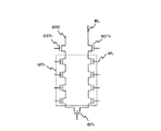
図3は例として積層導電層WLを6層積層したメモリセルアレイMAをビット線BL方向に沿って切断した断面図である。図3に示すように、メモリセルアレイMAはバックゲート層30と、メモリ層32と、選択トランジスタ層34と、配線層36とを有している。
FIG. 3 is a cross-sectional view of the memory cell array MA in which six stacked conductive layers WL are stacked as an example, cut along the bit line BL direction. As shown in FIG. 3, the memory cell array MA includes a
メモリセルアレイMAには、U字の柱状半導体層40が設けられている。柱状半導体層40は後述するバックゲートトランジスタ、メモリセルを構成するメモリトランジスタ、および選択トランジスタのチャネル(ボディ)として機能する。
A U-shaped
バックゲート層30では、U字の底部に当たる柱状半導体層40の周りに、ゲート絶縁膜(図示せず)、ゲート電極(図示せず)が設けられている。柱状半導体層40、ゲート絶縁膜、ゲート電極により、バックゲートトランジスタBTrが構成されている。
In the
メモリ層32では、U字の側部に当たる柱状半導体層40の周りに電荷蓄積層(図示せず)としてMONOS層(Metal Nitride Oxide Semiconductor)が設けられている。MONOS層を挟んで柱状半導体層40の周りにはゲート電極となる積層導電層WLが設けられている。柱状半導体層40、MONOS層、積層導電層WLにより、直列に接続された複数のメモリトランジスタMTrが構成されている。積層導電層WLはワード線WLでもある。
In the
MONOS層に電子がトラップされているか否かによって、メモリトランジスタMTrのしきい値が異なる。異なるしきい値状態が0/1の記憶状態に対応している。 The threshold value of the memory transistor MTr varies depending on whether electrons are trapped in the MONOS layer. Different threshold states correspond to 0/1 storage states.
選択トランジスタ層34では、U字の上端部に当たる柱状半導体層40の周りに、ゲート絶縁膜(図示せず)、ゲート電極(図示せず)が設けられている。柱状半導体層40、ゲート絶縁膜、ゲート電極により、選択トランジスタSSTr、SDTrが形成されている。
In the
バックゲートトランジスタBTr、複数のメモリトランジスタMTr、選択トランジスタSSTr、SDTrが直列接続され、メモリストリングMSが構成されている。 A back gate transistor BTr, a plurality of memory transistors MTr, and select transistors SSTr, SDTr are connected in series to form a memory string MS.
配線層36では、コンタクトプラグ41、42を介してメモリストリングMSの一端にビット線BLが接続されている。コンタクトプラグ41を介してメモリストリングMSの他端にソース線SRCが接続されている。
In the
隣接するメモリストリングMSは同じソース線SRCに接続されている。同じソース線SRCに接続されているメモリストリングMSの間に一定の間隔(P4)で直線状の柱状半導体層43が設けられている。柱状半導体層43はダミーの柱状半導体層である。柱状半導体層43の一端はソース線SRCに接続され、他端は開放されている。
Adjacent memory strings MS are connected to the same source line SRC. Linear columnar semiconductor layers 43 are provided at regular intervals (P4) between the memory strings MS connected to the same source line SRC. The
ダミーの柱状半導体層43の間に配置されている複数のメモリストリングMSを含んでメモリブロックMBが構成されている。 A memory block MB is configured including a plurality of memory strings MS disposed between the dummy columnar semiconductor layers 43.
NANDフラッシュメモリでは、多数のメモリセルにソース線を共有させる構成であるため、書き込みは複数のメモリセルからなる“ページ”という単位で行われ、また消去においては複数のページからなる“ブロック”という単位で行われる。なお、消去の単位は必ずしもブロック単位とは限られず、例えばブロックを複数に分割したグループごとに消去してもよい。 In the NAND flash memory, a source line is shared by a large number of memory cells, so that writing is performed in units of “pages” made up of a plurality of memory cells, and “blocks” made up of a plurality of pages in erasing. Done in units. The unit of erasure is not necessarily limited to a block unit, and for example, erasure may be performed for each group obtained by dividing a block into a plurality of groups.
データを読み出しまたは書き込みするとき、ブロックアドレスによりあるメモリブロックMBを選択して、選択されたモリブロックMB内のページ単位でデータの読み出しまたは書き込みを行う。消去については、例えばメモリブロックMB単位で行う。 When reading or writing data, a certain memory block MB is selected based on the block address, and data is read or written in units of pages in the selected memory block MB. Erasing is performed in units of memory blocks MB, for example.
各ページはワード線に対応している。ページとは、メモリブロックMBにおいて同じワード線WLに接続されているメモリトランジスタMTrのグループをいう。なお、ページは上記の定義に限られることなく、例えば共通するワード線WLに接続されているメモリセルトランジスタMTrの一部でページを構成してもよい。 Each page corresponds to a word line. A page refers to a group of memory transistors MTr connected to the same word line WL in the memory block MB. The page is not limited to the above definition. For example, the page may be configured by a part of the memory cell transistors MTr connected to the common word line WL.
但し、様々な理由によりダミーセルトランジスタが挿入される場合がある。この場合、ダミーセルトランジスタはページ数のカウントから除かれる。 However, a dummy cell transistor may be inserted for various reasons. In this case, the dummy cell transistor is excluded from the page count.
図4は、メモリストリングMSの等価回路を示す図である。図4に示すように、バックゲートトランジスタBTrの両側にそれぞれ複数のメモリトランジスタMTrが直列接続された直列回路が構成されている。 FIG. 4 is a diagram showing an equivalent circuit of the memory string MS. As shown in FIG. 4, a series circuit is configured in which a plurality of memory transistors MTr are connected in series on both sides of the back gate transistor BTr.
直列回路の一端側に選択トランジスタSDTrが接続され、直列回路の他端側に選択トランジスタSSTrが接続されている。選択トランジスタSDTrはビット線BLに接続され、選択トランジスタSSTrはソース線SRCに接続されている。 A selection transistor SDTr is connected to one end side of the series circuit, and a selection transistor SSTr is connected to the other end side of the series circuit. The selection transistor SDTr is connected to the bit line BL, and the selection transistor SSTr is connected to the source line SRC.
図5および図6はメモリアレイMA上の配線層36を示す平面図である。配線層36は、少なくともメモリアレイMA上に第1乃至第3配線層D0、D1、D2が設けられている。図5には、メモリアレイMA上の第1配線層D0と、第1配線層D0の上方に設けられる第2配線層D1が示されている。図6には、第2配線層D1と、第2配線層D1の上方に設けられる第3配線層D2が示されている。
5 and 6 are plan views showing the
図5に示すように、第1配線層D0には第1ピッチP1でワード線WL方向に延在する複数のソース線(第1ソース線)D0(SRC)が配列されている。ソース線D0(SRC)は図3に示すソース線SRCである。第2配線層D1には複数のビット線D1(BL)およびビット線D1(BL)と同じ方向に延在する複数のソース線(第2ソース線)D1(SRC)が設けられている。ビット線D1(BL)は図3に示すビット線BLである。 As shown in FIG. 5, a plurality of source lines (first source lines) D0 (SRC) extending in the direction of the word lines WL at the first pitch P1 are arranged in the first wiring layer D0. The source line D0 (SRC) is the source line SRC shown in FIG. The second wiring layer D1 is provided with a plurality of bit lines D1 (BL) and a plurality of source lines (second source lines) D1 (SRC) extending in the same direction as the bit lines D1 (BL). The bit line D1 (BL) is the bit line BL shown in FIG.
複数のソース線D1(SRC)は第2ピッチP2でワード線WL方向に配列されている。第2ピッチP2は、例えば512ビット線D1(BL)である。 The plurality of source lines D1 (SRC) are arranged in the word line WL direction at the second pitch P2. The second pitch P2 is, for example, a 512 bit line D1 (BL).
複数のソース線D0(SRC)はシャント46と呼ばれる領域で共通接続されている。シャント46は複数のソース線D0(SRC)と複数のソース線D1(SRC)の交差部に設けられている。複数のソース線D0(SRC)はシャント46にて第1コンタクトC1を介して、第2配線層D1のソース線D1(SRC)に電気的に接続されている。
A plurality of source lines D0 (SRC) are commonly connected in a region called a
メモリセルアレイMAをA−A線に沿って切断し、矢印方向から眺めた断面図が図3に示す断面図である。図3および図5において、個別に符号を付したソース線S1、S2、S3、S4は同じものである。 FIG. 3 is a cross-sectional view of the memory cell array MA taken along the line AA and viewed from the direction of the arrows. In FIG. 3 and FIG. 5, the source lines S1, S2, S3, and S4, which are individually labeled, are the same.
図6に示すように、第3配線層D2にはワード線WL方向に延在する複数のソース線(第3ソース線)D2(SRC)と、配線D2(CONT)が設けられている。複数のソース線D2(SRC)は第3ピッチP3でビット線BL方向に配列されている。第3ピッチP3は、例えば12ソース線D0(SRC)である。配線D2(CONT)はソース線D2(SRC)の間に設けられている。配線D2(CONT)は複数の細い配線を有している。 As shown in FIG. 6, the third wiring layer D2 is provided with a plurality of source lines (third source lines) D2 (SRC) extending in the word line WL direction and wirings D2 (CONT). The plurality of source lines D2 (SRC) are arranged in the bit line BL direction at the third pitch P3. The third pitch P3 is, for example, 12 source lines D0 (SRC). The wiring D2 (CONT) is provided between the source lines D2 (SRC). The wiring D2 (CONT) has a plurality of thin wirings.
ソース線D2(SRC)は、ソース線D1(SCR)より配線抵抗の小さいトップメタルである。ソース線D2(SRC)は、第2コンタクトC2を介してソース線D1(SCR)に電気的に接続されている。各ソース線D2(SRC)の一端は、図2に示すソース線ドライバ20に接続されている。
The source line D2 (SRC) is a top metal having a lower wiring resistance than the source line D1 (SCR). The source line D2 (SRC) is electrically connected to the source line D1 (SCR) through the second contact C2. One end of each source line D2 (SRC) is connected to the
配線D2(CONT)は、ロウデコーダ13、13a、センスアンプ14およびデータラッチ15の信号線等として使用されている。配線D2(CONT)は、直線状にレイアウトされている。
The wiring D2 (CONT) is used as signal lines for the
図7はソース線制御回路11を示す図である。図7に示すように、ソース線制御回路11はソース線ドライバ20と、ソース線の電圧をモニターするためのモニター配線(第1配線、第2配線)MON1、MON2と、ソース線モニター位置選択回路(選択回路)21と、ソース線電圧制御回路22を有している。
FIG. 7 is a diagram showing the source
モニター配線MON1およびソース線D2(SRC)は接続ノード(第1モニター位置)N1に接続されている。モニター配線MON2およびソース線D2(SRC)は接続ノード(第2モニター位置)N2に接続されている。ソース線モニター位置選択回路21は、デコード回路23と、スイッチ回路24を有している。
The monitor wiring MON1 and the source line D2 (SRC) are connected to a connection node (first monitor position) N1. The monitor wiring MON2 and the source line D2 (SRC) are connected to a connection node (second monitor position) N2. The source line monitor
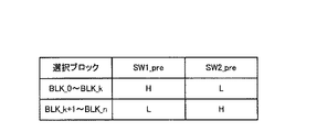
本明細書では、図2に示すメモリアレイMA中のメモリブロックMBの平面的配置に着目したときに、メモリアレイMAをメモリプレーンMPと称する。また、メモリブロック全体をさす場合、メモリブロックMBと記し、個別のメモリブロックはメモリブロックBLK_0乃至メモリブロックBLK_nと記す。 In this specification, when attention is paid to the planar arrangement of the memory blocks MB in the memory array MA shown in FIG. 2, the memory array MA is referred to as a memory plane MP. Further, when referring to the entire memory block, it is referred to as a memory block MB, and the individual memory blocks are referred to as memory blocks BLK_0 to BLK_n.
メモリプレーンMPは(n+1)個のメモリブロックBLK_0〜BLK_nを有している。メモリプレーンMPは第1の領域MP1と第2の領域MP2に分けられている。第1の領域MP1にはメモリブロックBLK_0〜BLK_kが配置され、第2の領域MP2にはメモリブロックBLK_k+1〜BKL_nが配置されている。 The memory plane MP has (n + 1) memory blocks BLK_0 to BLK_n. The memory plane MP is divided into a first area MP1 and a second area MP2. Memory blocks BLK_0 to BLK_k are arranged in the first area MP1, and memory blocks BLK_k + 1 to BKL_n are arranged in the second area MP2.
簡単のために、nは奇数とする。第1の領域MP1と第2の領域MP2に含まれるメモリブロックMBの数を等しくするために、k=(n−1)/2とする。 For simplicity, n is an odd number. In order to make the number of memory blocks MB included in the first area MP1 and the second area MP2 equal, k = (n−1) / 2.
各メモリブロックMBからそれぞれソース線D2(SRC)が引き出されている。引き出されたソース線D2(SRC)は、それぞれソース線ドライバ20のn型MOSトランジスタSTrに接続されている。
A source line D2 (SRC) is drawn from each memory block MB. The extracted source line D2 (SRC) is connected to the n-type MOS transistor STr of the
第1の領域MP1にあるソース線D2(SRC)の内、両端に配置されているメモリブロックBLK_0、BLK_kの中間、即ちメモリプレーンMPの一方の端からメモリプレーンMPの1/4の位置にあるメモリブロックBLK_k/2から引き出されたソース線D2(SRC)にモニター配線MON1が接続されている。 Among the source lines D2 (SRC) in the first region MP1, the memory blocks BLK_0 and BLK_k arranged at both ends are located in the middle of the memory blocks MP, that is, one-fourth of the memory plane MP from one end of the memory plane MP. A monitor wiring MON1 is connected to the source line D2 (SRC) drawn from the memory block BLK_k / 2.
同様に、第2の領域MP2にあるソース線D2(SRC)の内、両端に配置されているメモリブロックBLK_k+1、BLK_nの中間、即ちメモリプレーンMPの他方の端からメモリプレーンMPの1/4の位置にあるメモリブロックBLK_(n+k+1)/2から引き出されたソース線D2(SRC)にモニター配線MON2が接続されている。 Similarly, in the source line D2 (SRC) in the second region MP2, between the memory blocks BLK_k + 1 and BLK_n arranged at both ends, that is, from the other end of the memory plane MP to 1/4 of the memory plane MP. The monitor wiring MON2 is connected to the source line D2 (SRC) drawn from the memory block BLK_ (n + k + 1) / 2 at the position.
デコード回路23は選択されるメモリブロックMBを指定する制御信号Scをデコードして、選択されるメモリブロックMBが第1の領域MP1にあるか、または第2の領域MP2にあるかを示すデコード結果SW1_pre、SW2_preを出力する。
The
選択信号は、データを読み出すために選択されるメモリストリングMSのアドレス、または選択されるメモリストリングMSの属するメモリブロックMBのアドレスを含んでいる。 The selection signal includes the address of the memory string MS selected for reading data or the address of the memory block MB to which the selected memory string MS belongs.
図8はデコード回路23のデコード結果を示す図である。図8に示すように、選択されたメモリブロックMBが第1の領域MP1にあるメモリブロックBLK_0〜BLK_kのいずれかときに、デコード結果SW1_preをhighレベルにし、デコード結果SW2_preをlowレベルにする。
FIG. 8 is a diagram showing a decoding result of the
選択されたメモリブロックMBが第2の領域MP2にあるメモリブロックBLK_k+1〜BLK_nのいずれかのときに、デコード結果SW1_preをlowレベルにし、デコード結果SW2_preをhighレベルにする。 When the selected memory block MB is one of the memory blocks BLK_k + 1 to BLK_n in the second area MP2, the decoding result SW1_pre is set to the low level and the decoding result SW2_pre is set to the high level.
選択されたメモリブロックMBが第1の領域MP1および第2の領域MP2のいずれにもないときは、デコード結果SW1_pre、SW2_prをともにlowレベルにする。 When the selected memory block MB is not in either the first area MP1 or the second area MP2, the decoding results SW1_pre and SW2_pr are both set to the low level.
図9はスイッチ回路24を示す回路図である。図9に示すように、スイッチ回路24は2つのスイッチ素子SW1、SW2を有している。スイッチ素子SW1、SW2はともにn型MOSトランジスタである。スイッチ素子SW1では、ソース電極がモニター配線MON1に接続され、ゲート電極にレベルシフト回路LS1を介してデコード結果SW1_preが入力される。
FIG. 9 is a circuit diagram showing the
同様にスイッチ素子SW2では、ソース電極がモニター配線MON2に接続され、ゲート電極にレベルシフト回路LS2を介してデコード結果SW2_preが入力される。2つのドレイン電極は互いに接続されている。レベルシフト回路LS1、LS2はそれぞれデコード結果SW1_pre、SW2_preの電圧レベルをn型MOSトランジスタの動作レベルに合わせるために用いている。 Similarly, in the switch element SW2, the source electrode is connected to the monitor wiring MON2, and the decode result SW2_pre is input to the gate electrode via the level shift circuit LS2. The two drain electrodes are connected to each other. The level shift circuits LS1 and LS2 are used to adjust the voltage levels of the decoding results SW1_pre and SW2_pre to the operation level of the n-type MOS transistor, respectively.
スイッチ回路24は以下のように動作する。デコード結果SW1_preがhighレベルの時はスイッチ素子SW1がオン、スイッチSW2がオフになる。デコード結果SW2_preがhighレベルの時はスイッチ素子SW1がオフ、スイッチSW2がオンになる。
The
スイッチ素子SW1がオンのとき、接続ノードN1におけるソース線電圧が出力端子MONOUTから出力される。一方、スイッチ素子SW2がオンのとき、接続ノードN2におけるソース線電圧が出力端子MONOUTから出力される。 When the switch element SW1 is on, the source line voltage at the connection node N1 is output from the output terminal MONOUT. On the other hand, when the switch element SW2 is on, the source line voltage at the connection node N2 is output from the output terminal MONOUT.
即ち、メモリブロックBLK_0〜BLK_kのいずれか1つが選択された場合に、モニター配線MON1がソース線電圧制御回路22の非反転入力端子に接続される。メモリブロックBLK_k+1〜BLK_nのいずれか1つが選択された場合に、モニター配線MON2がソース線電圧制御回路22の非反転入力端子に接続される。
That is, when any one of the memory blocks BLK_0 to BLK_k is selected, the monitor wiring MON1 is connected to the non-inverting input terminal of the source line
スイッチ回路24は、さらにNOR回路24aおよびn型MOSトランジスタ24bを有している。NOR回路24aの2つの入力端子はそれぞれモニター配線MON1、MON2に接続されている。n型MOSトランジスタ24bは出力端子MONOUTと接地端子GNDとの間に接続されている。n型MOSトランジスタ24bのゲート電極は、NOR回路24aの出力端子に接続されている。
The
デコード結果SW1_pre、SW2_preがともにlowレベルのときに、n型MOSトランジスタ24bがオンになる。スイッチ回路24はリセットされ、スイッチ素子SW1、SW2はオフになる。
When the decoding results SW1_pre and SW2_pre are both at the low level, the n-
ソース線電圧制御回路22は差動回路、例えば演算増幅器である。演算増幅器の非反転入力端子はソース線モニター位置選択回路21に接続され、反転入力端子は基準電圧Vrefを出力する電源(図示せず)に接続され、出力端子はソース線ドライバ20のトランジスタSTrのゲート電極に接続されている。
The source line
ソース線電圧制御回路22は、デコード回路23のデコード結果SW1_pre、SW2_preに応じて接続ノードN1または接続ノードN2におけるソース線電圧Vsrcが基準電圧Vrefに等しくなるように動作する。接続ノードN1、N2をソース線モニター位置N1、N2とも称する。
The source line
ソース線モニター位置N1またはソース線モニター位置N2におけるソース線D2(SRC)の電圧Vsrcが基準電圧Vrefに等しくなる。 The voltage Vsrc of the source line D2 (SRC) at the source line monitor position N1 or the source line monitor position N2 becomes equal to the reference voltage Vref.
ソース線モニター位置N1、N2は、ソース線ドライバ20と、メモリプレーンMPの間に設けられる。一方、モニター配線MON1、MON2は、例えば配線層36の第2配線層D2にソース線D2(SRC)とともに設けられる。
The source line monitor positions N1 and N2 are provided between the
図10はデータを読み出す動作を示すタイミングチャートである。図10に示すように、メモリセルの読み出し動作は、選択されたワード線WLに読み出し電圧VCGを印加し、非選択のワード線WLに読み出し電圧VCGより高い読み出し非選択電圧VREADを印加する。 FIG. 10 is a timing chart showing an operation of reading data. As shown in FIG. 10, in the read operation of the memory cell, the read voltage VCG is applied to the selected word line WL, and the read non-select voltage VREAD higher than the read voltage VCG is applied to the non-selected word line WL.
選択トランジスタSDTr、SSTrのゲート電極に、しきい値より高い電圧VSGを印加する。選択トランジスタSDTr、SSTrはオン状態になり、メモリストリグMSがソース線SRCおよびビット線BLと導通する。 A voltage VSG higher than the threshold value is applied to the gate electrodes of the selection transistors SDTr and SSTr. The selection transistors SDTr and SSTr are turned on, and the memory string MS is electrically connected to the source line SRC and the bit line BL.
これにより、ビット線BLの電圧Vblとソース線SRCの電圧Vsrcの差(ΔV=Vbl−Vsrc)がメモリストリングMS間に印加される。この時、選択されたメモリブロックMB内の選択されたメモリストリングMSには、ビット線からソース線に向かって電流が流れる。選択されたメモリストリングMSに電流が流れるか否かによってデータの読み出しがおこなわれる。 Thereby, the difference (ΔV = Vbl−Vsrc) between the voltage Vbl of the bit line BL and the voltage Vsrc of the source line SRC is applied between the memory strings MS. At this time, a current flows from the bit line toward the source line in the selected memory string MS in the selected memory block MB. Data is read out depending on whether or not a current flows through the selected memory string MS.
次に、本実施形態のソース線制御回路11の効果について、比較例のソース線制御回路と対比して説明する。
Next, the effect of the source
図11はソース線制御回路11をソース線D1(SCR)およびソース線D2(SRC)との接続関係に着目して示す図である。図12は比較例のソース線制御回路をソース線D1(SCR)およびソース線D2(SRC)の接続関係に着目して示す図である。
FIG. 11 is a diagram showing the source
始めに、比較例のソース線制御回路について説明する。図12に示すように、比較例のソース線制御回路100は、ソース線ドライバ20と、ソース線電圧制御回路22を有することは、本実施形態のソース線制御回路11と同じである。
First, a source line control circuit of a comparative example will be described. As shown in FIG. 12, the source
異なるのは、ソース線制御回路11が分散してソース線D2(SRC)に接続された2つのモニター配線MON1、MON2と、ソース線モニター位置選択回路21を有するのに対して、ソース線制御回路100は中央に位置するソース線D2(SRC)に接続ノードN0で接続されたモニター配線MON0のみを有することにある。ノードN0をソース線モニター位置N0とも称する。
The difference is that the source
比較例のソース線制御回路100では、ソース線電圧制御回路22は、中央のソース線モニター位置N0においてソース線の電圧Vsrcが基準電圧Vrefに等しくなるように動作する。
In the source
ところで、メモリトランジスタMTrのしきい値を負の領域に書き込む場合もしくは、選択トランジスタSDTr、SSTrのしきい値が負の場合、しばしば読み出し時にソース線SRCに正の電圧をかけて読み出す方式が採用される。 By the way, when the threshold value of the memory transistor MTr is written in the negative region or when the threshold value of the selection transistors SDTr and SSTr is negative, a method of reading by applying a positive voltage to the source line SRC at the time of reading is often adopted. The
例えばソース線SRCに正の電圧をかけた状態で、選択されたメモリトランジスタMTrのゲート電極(即ち、選択されたワード線WL)に印加する読み出し電圧VCGを正の電圧よりも低くすれば選択されたメモリトランジスタMTrのゲート・ソース間電圧Vgsはマイナスになる為、負のしきい値を読み出すことが可能となる。 For example, when a positive voltage is applied to the source line SRC, the read voltage VCG applied to the gate electrode (ie, the selected word line WL) of the selected memory transistor MTr is set lower than the positive voltage. Since the gate-source voltage Vgs of the memory transistor MTr becomes negative, a negative threshold value can be read out.
また、選択トランジスタSDTr、SSTrのしきい値が負の場合、非選択のメモリストリングMSにも意図しないセル電流が流れる。しかし、ソース線SRCに正の電圧をかけると、選択トランジスタSDTr、SSTrのゲート・ソース間電圧Vgsを負にすることができる。その結果、選択トランジスタSDTr、SSTrがカットオフになり、非選択のメモリストリングMSに電流が流れるのを抑制できる。 In addition, when the threshold values of the selection transistors SDTr and SSTr are negative, an unintended cell current flows also in the non-selected memory string MS. However, when a positive voltage is applied to the source line SRC, the gate-source voltage Vgs of the selection transistors SDTr and SSTr can be made negative. As a result, the selection transistors SDTr and SSTr are cut off, and current can be suppressed from flowing through the non-selected memory strings MS.
理想的には、ソース線SRCの電位は選択されたメモリブロックMBの位置に依らず常に一定の値になることが望ましい。 Ideally, it is desirable that the potential of the source line SRC always has a constant value regardless of the position of the selected memory block MB.
然し、比較例のソース線制御回路100ではソース線D2(SRC)の電圧を所定の範囲内に保つことは難しい。以下に、その理由を説明する。
However, it is difficult for the source
メモリブロックMBはソース線ドライバ20と直交する方向に配置されている。セル電流はシャント46でメモリアレイMA上の第1配線層D0のソース線D0(SRC)および第2配線層D1のソース線D1(SRC)を通して横方向に拡散するように流れる。
The memory block MB is arranged in a direction orthogonal to the
しかし、前述したようにメモリアレイMA上の第3配線層D2のソース線D2(SRC)が最も低抵抗であり、かつ第3配線層D2は直線状にレイアウトされているため、ソース線D1(SRC)に流れ込んだセル電流はあまり横方向に拡散せず、ほぼ選択されたメモリブロックMBの直上にあるソース線D2(SRC)に集中して流れる。 However, as described above, since the source line D2 (SRC) of the third wiring layer D2 on the memory array MA has the lowest resistance and the third wiring layer D2 is laid out in a straight line, the source line D1 ( The cell current that has flowed into the SRC) does not diffuse much in the lateral direction, and concentrates on the source line D2 (SRC) directly above the selected memory block MB.
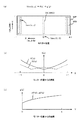
図13はソース線ドライバ20に流れ込む電流の分布を示す図である。図13において、横軸はメモリブロックMBの位置を示している。縦軸はソース線ドライバ20の各トランジスタSTrに流れる電流を示している。パラメータは選択されたメモリブロックMBの位置である。
FIG. 13 is a diagram showing a distribution of current flowing into the
電流分布a(実線)は、中央に位置するメモリブロックMBが選択されたとき、各トランジスタSTrに流れる電流を示している。電流分布b(一点鎖線)は、端に位置するメモリブロックMBが選択されたとき、各トランジスタSTrに流れる電流を示している。電流分布c(破線)は、端と中央の中間に位置するメモリブロックMBが選択されたとき、各トランジスタSTrに流れる電流を示している。従って、各電流分布a、b、cの積分値がソース線ドライバ20に流れ込むトータル電流である。
A current distribution a (solid line) indicates a current flowing through each transistor STr when the memory block MB located at the center is selected. A current distribution b (one-dot chain line) indicates a current flowing through each transistor STr when the memory block MB located at the end is selected. A current distribution c (broken line) indicates a current flowing through each transistor STr when a memory block MB located between the end and the center is selected. Therefore, the integrated value of each current distribution a, b, c is the total current flowing into the
図13に示すように、ソース線ドライバ20に流れ込む電流の分布は選択されたメモリブロックMBの位置によって異なっている。メモリプレーンMPの中央に位置するメモリブロックMBが選択された場合は、ソース線D0(SRC)に流れ込んだセル電流は横方向にある程度拡散し、中央に位置するソース線D2(SCR)に流れ込む電流が最も大きくなるように流れる(電流分布a)。
As shown in FIG. 13, the distribution of current flowing into the
メモリプレーンMPの端に位置するメモリブロックMBが選択された場合は、電流の拡散が一方向に制限されるため、ほぼすべてのセル電流がソース線ドライバ20の端のトランジスタSTrに集中するようになる(電流分布b)。
When the memory block MB located at the end of the memory plane MP is selected, current diffusion is limited in one direction, so that almost all cell current is concentrated in the transistor STr at the end of the
メモリプレーンMPの中央と端の中間に位置するメモリブロックMBが選択された場合は、電流の拡散が偏るため、電流分布aと電流分布bの中間の電流分布を示す(電流分布c)。 When the memory block MB located between the center and the end of the memory plane MP is selected, the current diffusion is biased, so that an intermediate current distribution between the current distribution a and the current distribution b is shown (current distribution c).
本実施形態のソース線制御回路11と比較例のソース線制御回路100では、ソース線ドライバ20に流れ込む電流の分布は図13に示すように基本的に同じである。
In the source
然しながら、比較例のソース線制御回路100では、メモリプレーンMPの中央に位置するメモリブロックMBが選択された場合、中央に位置するメモリブロックMBのソース線ドライバ20にもっとも近い箇所でソース線D2(SCR)の電圧Vsrcは基準電圧Vrefに等しくなる。
However, in the source
ソース線ドライバ20から遠くなるにつれてセル電流とメモリセルアレイMA内のソース線の配線抵抗によりソース線D2(SCR)の電圧Vsrcは基準電圧Vrefよりも大きくなる。
As the distance from the
メモリプレーンMPの端に位置するメモリブロックMBが選択された場合、ソース線モニター位置N0、即ち中央に位置するソース線D2(SCR)に接続されているソース線ドライバ20のトランジスタSTrCよりも、メモリプレーンMPの端に位置するソース線D2(SCR)に接続されているソース線ドライバ20のトランジスタSTrEにセル電流が集中して流れる。
When the memory block MB located at the end of the memory plane MP is selected, the memory is more memory than the transistor STrC of the
しかし、ソース線ドライバ20の各トランジスタSTrはゲート電極が共通接続されているので、各トランジスタSTrのゲート電圧Vgsはいずれも等しい。その結果、メモリプレーンMPの端に位置するソース線D2(SCR)に接続されているトランジスタSTrEのドレイン・ソース間電圧Vdsは中央に位置するソース線D2(SCR)に接続されているトランジスタSTrCのドレイン・ソース間電圧Vdsよりも高くなる。
However, since the gate electrodes of the transistors STr of the
図14は選択されたメモリブロックMBの位置とソース線モニター位置Nxからの配線抵抗の関係を示す図である。図14に示すようにソース線はビット線BL方向に配置された配線抵抗Rscr1とワード線WL方向に配置された配線抵抗Rscr2とが格子状に接続されている。 FIG. 14 is a diagram showing the relationship between the position of the selected memory block MB and the wiring resistance from the source line monitor position Nx. As shown in FIG. 14, in the source line, a wiring resistance Rscr1 arranged in the bit line BL direction and a wiring resistance Rscr2 arranged in the word line WL direction are connected in a grid pattern.
ここで、配線抵抗Rscr1はソース線D1(SRC)の配線抵抗、配線抵抗Rscr2はソース線D2(SRC)の配線抵抗である。配線抵抗Rscr1は配線抵抗Rscr2より大きい。ソース線モニター位置Nxでのソース線の電圧Vsrcは基準電圧Vrefに等しい。ソース線モニター位置Nxとは、比較例のソース線モニター位置N0または本実施形態のソース線モニター位置N1を示している。 Here, the wiring resistance Rscr1 is the wiring resistance of the source line D1 (SRC), and the wiring resistance Rscr2 is the wiring resistance of the source line D2 (SRC). The wiring resistance Rscr1 is larger than the wiring resistance Rscr2. The source line voltage Vsrc at the source line monitor position Nx is equal to the reference voltage Vref. The source line monitor position Nx indicates the source line monitor position N0 of the comparative example or the source line monitor position N1 of the present embodiment.
メモリプレーンMPの端のメモリブロックBLK1が選択された場合、メモリブロックBLK1はソース線モニター位置Nxから離れているので、メモリプレーンMP内のビット線BL方向の配線抵抗Rscr1が見える。その結果、ソース線配線抵抗Rscr1による電圧降下分だけソース線電圧Vsrcが高くなる。 When the memory block BLK1 at the end of the memory plane MP is selected, since the memory block BLK1 is away from the source line monitor position Nx, the wiring resistance Rscr1 in the direction of the bit line BL in the memory plane MP can be seen. As a result, the source line voltage Vsrc increases by the voltage drop due to the source line wiring resistance Rscr1.
図15はソース線ドライバ20から最も近いソース線位置B−Bでのソース線D2(SCR)の電圧分布を、比較例と対比して示す図で、図15(a)は本実施形態のソース線D2(SCR)の電圧分布、図15(b)は比較例のソース線D2(SCR)の電圧分布を示す図である。
FIG. 15 is a diagram showing the voltage distribution of the source line D2 (SCR) at the source line position BB closest to the
図16はソース線ドライバ20から最も遠いソース線位置C−Cでのソース線D2(SCR)の電圧分布を、比較例と対比して示す図で、図16(a)は本実施形態のソース線D2(SCR)の電圧分布、図16(b)は比較例のソース線D2(SCR)の電圧分布を示す図である。
FIG. 16 is a diagram showing the voltage distribution of the source line D2 (SCR) at the source line position C-C farthest from the
図15および図16において、横軸はメモリブロックMBの位置を示している。縦軸はソース線D2(SCR)の電圧Vsrcを示している。パラメータは選択されたメモリブロックMBの位置である。 15 and 16, the horizontal axis indicates the position of the memory block MB. The vertical axis represents the voltage Vsrc of the source line D2 (SCR). The parameter is the position of the selected memory block MB.
図15および図16において、電圧分布a(実線)は、中央に位置するメモリブロックMBが選択されたときのソース線D2(SCR)の電圧分布を示している。電圧分布b(一点鎖線)は、端に位置するメモリブロックMBが選択されたときのソース線D2(SCR)の電圧分布を示している。電圧分布c(破線)は、端と中央の中間に位置するメモリブロックMBが選択されたときのソース線D2(SCR)の電圧分布を示している。 15 and 16, the voltage distribution a (solid line) indicates the voltage distribution of the source line D2 (SCR) when the memory block MB located in the center is selected. The voltage distribution b (one-dot chain line) indicates the voltage distribution of the source line D2 (SCR) when the memory block MB located at the end is selected. A voltage distribution c (broken line) indicates the voltage distribution of the source line D2 (SCR) when the memory block MB located between the end and the center is selected.
始めに、比較例について説明する。図15(b)に示すように、比較例では、ソース線位置B−Bでのソース線D2(SCR)の電圧Vsrcは、ソース線モニター位置N0では基準電圧Vrefに等しい。 First, a comparative example will be described. As shown in FIG. 15B, in the comparative example, the voltage Vsrc of the source line D2 (SCR) at the source line position BB is equal to the reference voltage Vref at the source line monitor position N0.
中央のメモリブロックBLK_kが選択されたときのソース線の電圧分布aは、図13に示す電流分布aに倣って中央でピークを示し、両端に向かって減少するカーブを示している。そのカーブは略左右対称である。 The voltage distribution a of the source line when the center memory block BLK_k is selected shows a curve that shows a peak at the center and decreases toward both ends, following the current distribution a shown in FIG. The curve is substantially symmetrical.
一端のメモリブロックBLK_0が選択されたときのソース線の電圧分布bは、図13に示す電流分布bに倣って一端から他端に向かって減少し、他端側で一定値に漸近するカーブを示している。 The voltage distribution b of the source line when the memory block BLK_0 at one end is selected follows a current distribution b shown in FIG. 13 and decreases from one end to the other end, and ascends to a constant value at the other end side. Show.
中間のメモリブロックBLK_k/2が選択されたときのソース線の電圧分布cは、図13に示す電流分布cに倣って中間でピークを示し、一端側では電圧分布aに近く、他端側では電圧分布bに近いカーブを示している。 The voltage distribution c of the source line when the intermediate memory block BLK_k / 2 is selected shows a peak in the middle following the current distribution c shown in FIG. 13, close to the voltage distribution a on one end side, and on the other end side. A curve close to the voltage distribution b is shown.
これは、ビット線BL方向においてソース線モニター位置N0から遠ざかるほど配線抵抗が増加し、配線抵抗の増加に応じて電圧降下が増加することを示している。 This indicates that the wiring resistance increases with increasing distance from the source line monitor position N0 in the bit line BL direction, and the voltage drop increases as the wiring resistance increases.
一方、図15(a)に示すように、本実施形態では、ソース線位置B−Bでのソース線D2(SCR)の電圧Vsrcは、ソース線モニター位置N1において基準電圧Vrefに等しい。 On the other hand, as shown in FIG. 15A, in the present embodiment, the voltage Vsrc of the source line D2 (SCR) at the source line position BB is equal to the reference voltage Vref at the source line monitor position N1.
従って、本実施形態のソース線の電圧分布a、b、cは、基本的にそれぞれ比較例のソース線の電圧分布a、b、cをソース線モニター位置N1におけるソース線電圧Vsrcが基準電圧Vrefになるようにレベルシフトした分布を示している。 Therefore, the source line voltage distributions a, b, and c of the present embodiment are basically the same as the source line voltage distributions a, b, and c of the comparative example, respectively, and the source line voltage Vsrc at the source line monitor position N1 is the reference voltage Vref. The level shifted distribution is shown.
具体的には、本実施形態の電圧分布aは、比較例のソース線の電圧分布aがΔVaだけレベルアップされた分布に略等しくなる。本実施形態の電圧分布bは、比較例のソース線の電圧分布bがΔVbだけレベルダウンされた分布に略等しくなる。本実施形態の電圧分布cは、比較例のソース線の電圧分布cがΔVcだけレベルダウンされた分布に略等しくなる。 Specifically, the voltage distribution a of the present embodiment is substantially equal to a distribution obtained by leveling up the voltage distribution a of the source line of the comparative example by ΔVa. The voltage distribution b of the present embodiment is substantially equal to a distribution in which the voltage distribution b of the source line of the comparative example is leveled down by ΔVb. The voltage distribution c of the present embodiment is substantially equal to a distribution obtained by leveling down the voltage distribution c of the source line of the comparative example by ΔVc.
ΔVaは中間における比較例の電圧分布aのソース線電圧Vsrcと基準電圧Vrefとの差を示している。ΔVbは中間における比較例の電圧分布bのソース線電圧Vsrcと基準電圧Vrefとの差を示している。ΔVcは中間における比較例の電圧分布cのソース線電圧Vsrcと基準電圧Vrefとの差を示している。 ΔVa indicates the difference between the source line voltage Vsrc and the reference voltage Vref of the voltage distribution a of the comparative example in the middle. ΔVb indicates a difference between the source line voltage Vsrc of the voltage distribution b of the comparative example in the middle and the reference voltage Vref. ΔVc indicates the difference between the source line voltage Vsrc and the reference voltage Vref in the voltage distribution c of the comparative example in the middle.
比較例のソース線の浮きVuの最大値は、一端に位置するメモリブロックBLK_0が選択されたときのVu2である。これに対して、本実施形態のソース線の浮きVuの最大値は、一端のメモリブロックBLK_0選択された場合のVu1である。Vu1とVu2は、Vu1=Vu2−ΔVbの関係にある。 The maximum value of the floating Vu of the source line in the comparative example is Vu2 when the memory block BLK_0 located at one end is selected. In contrast, the maximum value of the floating Vu of the source line in this embodiment is Vu1 when the memory block BLK_0 at one end is selected. Vu1 and Vu2 have a relationship of Vu1 = Vu2−ΔVb.
ここで、ソース線の浮きVuとは、選択されたメモリブロックMB中のソース線電圧Vsrcと基準電圧Vrefとの差を意味しており、Vu=Vsrc−Vrefで表わされる。 Here, the floating Vu of the source line means a difference between the source line voltage Vsrc and the reference voltage Vref in the selected memory block MB, and is expressed by Vu = Vsrc−Vref.
従って、本実施形態においては、ソース線の浮きVuの最大値が比較例より小さいので、ソース線の浮きVuが最大になるメモリブロックMBが選択された場合でもメモリブロックMBに適切なセル電流が流れるように設定されるビット線電圧Vblを低くすることができる。 Therefore, in this embodiment, since the maximum value of the floating Vu of the source line is smaller than that of the comparative example, even when the memory block MB that maximizes the floating Vu of the source line is selected, an appropriate cell current is supplied to the memory block MB. The bit line voltage Vbl set to flow can be lowered.
ソース線の浮きVuが最大値より小さい場合に、選択されたメモリブロックに適切なセル電流より大きなセル電流が流れて、無駄な電力が消費されるのを防止することが可能である。 When the floating line Vu of the source line is smaller than the maximum value, it is possible to prevent useless power from being consumed due to a cell current larger than an appropriate cell current flowing in the selected memory block.
また本実施形態の別の効果として、ソース線の浮きVuの最大値が比較例より小さくなるので、その分、シャント46の幅を細くする、シャント46のピッチを拡大する等により、チップサイズの削減を図ることが可能である。
As another effect of the present embodiment, the maximum value of the floating Vu of the source line is smaller than that of the comparative example. Therefore, by reducing the width of the
ソース線ドライバ20から最も遠いソース線位置C−Cにおけるソース線D2(SCR)の電圧分布は、図15(a)、図15(b)に示すソース線D2(SCR)の電圧分布と略同じ傾向を示している。
The voltage distribution of the source line D2 (SCR) at the source line position C-C farthest from the
図16(b)に示すように、ソース線位置C−Cにおける比較例のソース線D2(SCR)の電圧分布a、b、cは、図15(b)に示す電圧分布a、b、cがレベルアップされたようなカーブを示している。 As shown in FIG. 16B, the voltage distributions a, b, and c of the source line D2 (SCR) of the comparative example at the source line position C-C are the voltage distributions a, b, and c shown in FIG. Shows a curve that is leveled up.
同様に、図16(a)に示すように、ソース線位置C−Cにおける本実施形態のソース線D2(SCR)の電圧分布a、b、cは、図15(a)に示す電圧分布a、b、cがレベルアップされたようなカーブを示している。 Similarly, as shown in FIG. 16A, the voltage distributions a, b, and c of the source line D2 (SCR) of the present embodiment at the source line position C-C are the voltage distribution a shown in FIG. , B, and c are shown as curves.
これは、ワード線WL方向においてソース線モニター位置から遠ざかるほど配線抵抗が増加するので、配線抵抗の増加に応じて電圧降下が増加することを示している。 This indicates that the voltage drop increases as the wiring resistance increases because the wiring resistance increases as the distance from the source line monitor position increases in the word line WL direction.
ソース線位置C−Cにおいても、本実施形態のソース線の浮きVuの最大値Vu3は比較例のソース線の浮きVuの最大値Vu4より小さい(Vu3<Vu4)。 Also at the source line position CC, the maximum value Vu3 of the source line floating Vu of this embodiment is smaller than the maximum value Vu4 of the source line floating Vu of the comparative example (Vu3 <Vu4).
ソース線電圧の面内分布について、詳しく説明する。
図17はソース線電圧の面内分布のシミュレーション方法を説明するための図で、図17(a)はメモリプレーンMP内のX、Y座標の定義を示す図、図17(b)はX方向の電圧分布を表わす関数を模式的に示す図、図17(c)はY方向の電圧分布を表わす関数を模式的に示す図である。
The in-plane distribution of the source line voltage will be described in detail.
FIG. 17 is a diagram for explaining a method of simulating the in-plane distribution of the source line voltage. FIG. 17A shows the definition of the X and Y coordinates in the memory plane MP, and FIG. 17B shows the X direction. FIG. 17C is a diagram schematically illustrating a function representing the voltage distribution in the Y direction.
図17(a)に示すように、ビット線BL方向をX軸とし、ワード線WL方向をY軸とする。ソース線モニター位置N0をX、Y座標の原点(0,0)とする。一つのメモリプレーンMP内でのある位置(x,y)におけるソース線電圧Vsrc(x,y)は、原点(0,0)からの距離xの関数f(x)と距離yの関数g(y)の和で近似できるとする。ソース線電圧Vsrcは、次式で表わされる。
Vsrc(x、y)=f(x)+g(y)
図17(b)に示すように、比較例の関数f2(x)は原点から両端に向かって対称に単調増加し、下凸のカーブを描くとする。一方、本実施形態の関数f1(x)は中間から一端および中央に向かって単調増加し、W型のカーブを描くとする。
As shown in FIG. 17A, the bit line BL direction is taken as the X axis, and the word line WL direction is taken as the Y axis. Let the source line monitor position N0 be the origin (0, 0) of the X and Y coordinates. The source line voltage Vsrc (x, y) at a certain position (x, y) in one memory plane MP is a function f (x) of the distance x from the origin (0, 0) and a function g ( It can be approximated by the sum of y). Source line voltage Vsrc is expressed by the following equation.
Vsrc (x, y) = f (x) + g (y)
As shown in FIG. 17B, it is assumed that the function f2 (x) of the comparative example monotonously increases symmetrically from the origin toward both ends, and draws a downwardly convex curve. On the other hand, the function f1 (x) of this embodiment monotonously increases from the middle toward one end and the center, and draws a W-shaped curve.
図17(c)に示すように、比較例の関数g2(y)は原点から端に向かって単調に増加し、上凸のカーブを描くとする。本実施形態の関数g1(x)は関数g2(y)と略同じである。 As shown in FIG. 17C, it is assumed that the function g2 (y) of the comparative example monotonously increases from the origin toward the end and draws an upwardly convex curve. The function g1 (x) of this embodiment is substantially the same as the function g2 (y).
図18はソース線電圧Vsrcの面内分布をシミュレーションした結果示す等高線図で、図18(a)は本実施形態の等高線図、図18(b)は比較例の等高線図を示す図である。図18(a)および図18(b)において、等高線の間隔は20mVである。パラメータは選択されたメモリブロックMBの位置である。 FIG. 18 is a contour map showing the result of simulating the in-plane distribution of the source line voltage Vsrc, FIG. 18A is a contour map of the present embodiment, and FIG. 18B is a contour map of a comparative example. In FIG. 18A and FIG. 18B, the interval between the contour lines is 20 mV. The parameter is the position of the selected memory block MB.
図18(b)に示すように、比較例のソース線電圧の面内分布は、選択されたメモリブロックMBが中央から中間、一端に移るにつれて、一端側のソース線の電圧Vsrcが高くなる。ソース線モニター位置N0から最も遠い位置にあるソース線の電圧が最も高い。ソース線電圧の面内分布は、選択されたメモリブロックMBの位置によって変化する。 As shown in FIG. 18B, in the in-plane distribution of the source line voltage of the comparative example, the voltage Vsrc of the source line on one end side increases as the selected memory block MB moves from the center to the middle and one end. The voltage of the source line located farthest from the source line monitor position N0 is the highest. The in-plane distribution of the source line voltage varies depending on the position of the selected memory block MB.
一方、図18(a)に示すように、本実施形態のソース線電圧の面内分布は、ソース線モニター位置がN0からN1にシフトしたことに応じて、比較例のソース線電圧の面内分布が一端側にシフトしたような分布を示している。 On the other hand, as shown in FIG. 18A, the in-plane distribution of the source line voltage of the present embodiment is the in-plane distribution of the source line voltage of the comparative example according to the shift of the source line monitor position from N0 to N1. The distribution is such that the distribution is shifted to one end side.
ソース線モニター位置から選択されたメモリブロックMBまでの距離xの範囲が縮まる為である。その結果、ソース線電圧Vsrcの面内分布では、均一が比較例より向上している。 This is because the range of the distance x from the source line monitor position to the selected memory block MB is reduced. As a result, the uniformity of the in-plane distribution of the source line voltage Vsrc is improved as compared with the comparative example.
ここで、読み出しの際のビット線電圧Vblを考える。端のメモリブロックMBが選択された場合にソース線D2(SRC)の電圧Vsrcが最も高くなる。この場合においても、メモリストリングMSに適切な電圧(ビット線電圧とソース線電圧の差)が印加されるようにビット線電圧Vblが設定される。 Here, the bit line voltage Vbl at the time of reading is considered. When the end memory block MB is selected, the voltage Vsrc of the source line D2 (SRC) becomes the highest. Also in this case, the bit line voltage Vbl is set so that an appropriate voltage (difference between the bit line voltage and the source line voltage) is applied to the memory string MS.
例えば、端のメモリブロックMBを選択した場合、ビット線電圧Vblとソース線D2(SRC)の電圧との差を0.5vに設定する。中央のメモリブロックMBを選択した場合、ビット線電圧Vblとソース線D2(SRC)の電圧との差は0.5v以上になるため、セル電流が増加する。これは単に消費電力が増加することを示している。 For example, when the end memory block MB is selected, the difference between the bit line voltage Vbl and the voltage of the source line D2 (SRC) is set to 0.5v. When the central memory block MB is selected, since the difference between the bit line voltage Vbl and the source line D2 (SRC) is 0.5 V or more, the cell current increases. This simply indicates that the power consumption increases.
従って、ソース線の電圧Vsrcは選択されたメモリブロックMBの位置に依らず常に一定であることが望ましいが、ソース線の配線抵抗により必然的にソース線電圧Vsrcの選択ブロック位置依存性が生じる。 Therefore, it is desirable that the source line voltage Vsrc is always constant irrespective of the position of the selected memory block MB. However, the source line wiring resistance necessarily causes the source line voltage Vsrc to depend on the selected block position.
本実施形態では、ソース線電圧Vsrcの選択ブロック位置依存性を抑えているので、その分ビット線電圧Vblを下げることができる。従って、消費電力を削減することが可能である。 In this embodiment, since the dependency of the source line voltage Vsrc on the selected block position is suppressed, the bit line voltage Vbl can be lowered accordingly. Therefore, power consumption can be reduced.
また、ビット線電圧Vblを下げない場合においても、ソース線電圧Vsrcのワースト値を改善することができるので、その分ソース線シャント46の幅を細くする、第2ピッチを拡大する等により、セルアレイサイズの縮小を図ることが可能となる。
Even when the bit line voltage Vbl is not lowered, the worst value of the source line voltage Vsrc can be improved. Therefore, by reducing the width of the
以上説明したように、本実施形態の半導体不揮発性記憶装置10では、ソース線制御回路11は、ソース線モニター位置選択回路21と、ソース線電圧制御回路22とを有している。
As described above, in the semiconductor
ソース線モニター位置選択回路21は、選択されたメモリブロックMBの位置に応じて、ソース線モニター位置N1またはソース線モニター位置N2を選択する。ソース線電圧制御回路22は、選択されたソース線モニター位置N1またはソース線モニター位置N2においてソース線電圧Vsrcが基準電圧Vrefに等しくなるようにソース線ドライバ20を駆動する。
The source line monitor
その結果、ソース線電圧VsrcのメモリブロックMB位置依存性が低減するので、ソース線の浮きVuの最大値が小さくなる。その分ソース線の浮きVuの最大値に合わせて設定されるビット線電圧Vblを下げることができる。 As a result, the dependency of the source line voltage Vsrc on the memory block MB position is reduced, and the maximum value of the source line floating Vu is reduced. Accordingly, the bit line voltage Vbl set in accordance with the maximum value of the floating Vu of the source line can be lowered.
ビット線電圧Vblを下げることにより、選択されたメモリブロックMB内を流れる過剰なセル電流を抑制することができる。従って、消費電力の少ない不揮発性半導体記憶装置が得られる。 By reducing the bit line voltage Vbl, an excessive cell current flowing in the selected memory block MB can be suppressed. Therefore, a nonvolatile semiconductor memory device with low power consumption can be obtained.
ここでは、ソース線モニター位置N1、N2がメモリプレーンMPの中央と中間(端から全長に対して1/4の距離)にある場合について説明したが、ソース線モニター位置は特に限定されない。ソース線モニター位置は中間よりずらしても構わない。 Here, the case where the source line monitor positions N1 and N2 are in the middle and the middle of the memory plane MP (distance from the end to 1/4 of the total length) has been described, but the source line monitor position is not particularly limited. The source line monitor position may be shifted from the middle.
例えば、端のメモリブロックMBが選択された場合と中央のメモリブロックMBが選択された場合とで、ソース線の浮きが等しくなるように、ソース線モニター位置を調整することができる。 For example, the source line monitor position can be adjusted so that the floating of the source line is the same when the end memory block MB is selected and when the center memory block MB is selected.
図19はソース線モニター位置とX方向のソース線の電圧分布を表わす関数f(x)との関系を模式的に示す図である。図19において、実線は比較例の関数f2(x)を示している。破線は本実施形態の関数f1(x)を示している。一点鎖線はソース線モニター位置が中間より端に近い位置にある場合の関数f3(x)を示している。関数f1(x)、f2(x)は図17(b)に示す関数f1(x)、f2(x)である。 FIG. 19 is a diagram schematically showing the relationship between the source line monitor position and the function f (x) representing the voltage distribution of the source line in the X direction. In FIG. 19, the solid line indicates the function f2 (x) of the comparative example. The broken line indicates the function f1 (x) of this embodiment. The alternate long and short dash line indicates the function f3 (x) when the source line monitor position is closer to the end than the middle. The functions f1 (x) and f2 (x) are the functions f1 (x) and f2 (x) shown in FIG.
図19に示すように、ソース線モニター位置を中央から端に移動させるにつれて、中央のソース線電圧が増加し、端のソース線電圧が低下する。ソース線モニター位置が中間にある場合の関数f2(x)では、端のソース線電圧が中央のソース線電圧よりまだ高い。 As shown in FIG. 19, as the source line monitor position is moved from the center to the end, the center source line voltage increases and the end source line voltage decreases. In the function f2 (x) when the source line monitor position is in the middle, the end source line voltage is still higher than the central source line voltage.
ソース線モニター位置を更に中間より端側にずらすことにより、端のメモリブロックMBが選択された場合と、中央のメモリブロックMBが選択された場合とで、ソース線の浮きVu5を等しくすることが出来る。 By further shifting the source line monitor position from the middle to the end side, the source line floating Vu5 can be made equal between when the end memory block MB is selected and when the center memory block MB is selected. I can do it.
その結果、ビット線電圧VblをVu1−Vu5だけ下げられるので、過剰なセル電流が抑制される。消費電力を更に削減することが可能である。 As a result, the bit line voltage Vbl can be lowered by Vu1-Vu5, so that excessive cell current is suppressed. It is possible to further reduce power consumption.
第1の領域MP1および第2の領域MP2の境界が、メモリブロックMBの境界と一致する場合について説明したが、第1の領域MP1および第2の領域MP2の境界とメモリブロックMBの境界は一致しなくても構わない。 Although the case where the boundary between the first area MP1 and the second area MP2 coincides with the boundary of the memory block MB has been described, the boundary between the first area MP1 and the second area MP2 and the boundary between the memory blocks MB are identical. You don't have to.
図20は第1の領域MP1および第2の領域MP2の境界とメモリブロックMBの境界が一致しない場合のメモリセルアレイMAの断面図である。図20に示すように、中央のメモリブロックBLK_kとメモリブロックBLK_k+1の境界をB1とし、第1の領域MP1および第2の領域MP2の境界をB2とする。 FIG. 20 is a cross-sectional view of the memory cell array MA when the boundary between the first region MP1 and the second region MP2 does not coincide with the boundary of the memory block MB. As shown in FIG. 20, the boundary between the central memory block BLK_k and the memory block BLK_k + 1 is B1, and the boundary between the first region MP1 and the second region MP2 is B2.
メモリブロックMBの境界B1には、図3に示すダミーの柱状半導体層43が設けられている。第1の領域MP1および第2の領域MP2の境界B2は、境界B2よりメモリストリングMS一個分だけ一端側にシフトして定められている。
A dummy
シフトするメモリストリングMSの数は特に限定されない。即ち、第1の領域MP1および第2の領域MP2の境界B2の位置は、特に限定されない。メモリストリングMSはデータを読み出すための最小単位なので、境界B2の位置は隣接するメモリストリングMSの間であればよい。従って、境界B2の位置をより細かく設定することが可能になる。 The number of memory strings MS to be shifted is not particularly limited. That is, the position of the boundary B2 between the first region MP1 and the second region MP2 is not particularly limited. Since the memory string MS is the minimum unit for reading data, the position of the boundary B2 may be between adjacent memory strings MS. Therefore, the position of the boundary B2 can be set more finely.
メモリブロックMBの境界B1と第1の領域MP1および第2の領域MP2の境界B2は、一致しなくても特に不具合は生じない。 Even if the boundary B1 of the memory block MB and the boundary B2 of the first region MP1 and the second region MP2 do not coincide with each other, no particular problem occurs.
(実施形態2)
本実施形態に係る不揮発性半導体記憶装置について、図21および図22を用いて説明する。図21は本実施形態の不揮発性半導体記憶装置のメモリセルアレイを含む周辺回路を示すブロック図、図22はソース線の電圧分布のモデルを示す図である。
(Embodiment 2)
The nonvolatile semiconductor memory device according to this embodiment will be described with reference to FIGS. FIG. 21 is a block diagram showing a peripheral circuit including a memory cell array of the nonvolatile semiconductor memory device of this embodiment, and FIG. 22 is a diagram showing a model of voltage distribution of the source line.
本実施形態において、上記実施形態1と同一の構成部分には同一符号を付してその部分の説明は省略し、異なる部分について説明する。本実施形態が実施形態1と異なる点は、ソース線ドライバがメモリセルアレイの両側に配置されていることにある。 In the present embodiment, the same components as those in the first embodiment are denoted by the same reference numerals, description thereof will be omitted, and different portions will be described. The present embodiment is different from the first embodiment in that source line drivers are arranged on both sides of the memory cell array.
図21に示すように、本実施形態の不揮発性半導体記憶装置50では、ソース線ドライバ20aはロウデコーダ13aを挟んでメモリセルアレイMAの他側に配置されている。ソース線ドライバ20aは、ソース線ドライバ20と同じ構成である。ソース線ドライバ20aは図7に示すゲート電極が共通接続された複数のMOSトランジスタSTrを有している。
As shown in FIG. 21, in the nonvolatile
ソース線ドライバ20aにおいて、複数のMOSトランジスタSTrはそれぞれ複数のソース線D2(SRC)の他端(ソース線位置C−C側)に接続されている。MOSトランジスタSTrのゲート電極はソース線電圧制御回路22の出力端子に接続されている。
In the
ソース線電圧制御回路22は、ソース線ドライバ20のMOSトランジスタSTrおよびソース線ドライバ20aのMOSトランジスタSTrを同時に駆動する。その結果、第1および第2電流経路が形成される。
The source line
第1電流経路は、図7に示すセル電流がソース線D2(SRC)からソース線ドライバ20を通って接地端子GNDに流れる電流経路である。第2電流経路はセル電流がソース線D2(SRC)からソース線ドライバ20aを通って接地端子GNDに流れる電流経路である。
The first current path is a current path in which the cell current shown in FIG. 7 flows from the source line D2 (SRC) through the
セル電流は第1および第2電流経路に分流されるので、図14に示すワード線WL方向の配線抵抗Rscr2は実質的に1/2になる。例えば、図14に示すメモリプレーンMPの中央のメモリブロックBLK3が選択され、メモリブロックBLK3の中央のメモリストリングMSにセル電流が流れる場合、セル電流はソース線ドライバ20aを流れる電流とソース線ドライバ20を流れる電流に2等分される。
Since the cell current is divided into the first and second current paths, the wiring resistance Rscr2 in the word line WL direction shown in FIG. 14 is substantially halved. For example, when the memory block BLK3 at the center of the memory plane MP shown in FIG. 14 is selected and a cell current flows through the memory string MS at the center of the memory block BLK3, the cell current is the current flowing through the
また、メモリブロックBLK3の中央以外のメモリストリングMSにセル電流が流れる場合、セル電流はソース線ドライバ20、20aのどちらか近いほうに優先的に流れる。
In addition, when a cell current flows through the memory string MS other than the center of the memory block BLK3, the cell current flows preferentially to one of the
図22は、本実施形態のソース線の電圧分布を表わす関数g3(y)を図17(c)に示す実施形態1のソース線の電圧分布を表わす関数g1(y)、g2(y)対比して示す図である。図22に示すように、本実施形態の関数g3(y)は上凸のカーブを描き、電圧分布関数g1(y)より小さくなる。 22 compares the function g3 (y) representing the voltage distribution of the source line of this embodiment with the functions g1 (y) and g2 (y) representing the voltage distribution of the source line of the first embodiment shown in FIG. 17 (c). It is a figure shown. As shown in FIG. 22, the function g3 (y) of this embodiment draws an upwardly convex curve and is smaller than the voltage distribution function g1 (y).
その結果、Y方向のソース線の浮きの最大値が低減するので、消費電力を更に低減することが可能である。 As a result, since the maximum value of the floating of the source line in the Y direction is reduced, the power consumption can be further reduced.
以上説明したように、本実施形態の不揮発性半導体記憶装置50では、ソース線ドライバ20、20aがワード線方向に沿ってメモリセルアレイMAの両側に配置され、ソース線D2(SRC)の両端に接続されている。
As described above, in the nonvolatile
その結果、第1、第2電流経路が形成されるので、ワード線WL方向の配線抵抗Rscr2は実質的に1/2になる。従って、Y方向のソース線の浮きの最大値が低減し、消費電力を更に低減することができる利点がある。 As a result, since the first and second current paths are formed, the wiring resistance Rscr2 in the word line WL direction is substantially halved. Therefore, there is an advantage that the maximum value of the floating of the source line in the Y direction can be reduced and the power consumption can be further reduced.
ここでは、2つのソース線ドライバがメモリセルアレイMAの両側に配置されている場合について説明したが、複数のソース線ドライバをメモリセルアレイMAのワード線WL方向に沿って分散して配置してもよい。 Here, a case where two source line drivers are arranged on both sides of the memory cell array MA has been described, but a plurality of source line drivers may be distributed along the word line WL direction of the memory cell array MA. .
例えば、3つのソース線ドライバをワード線方向に沿ってメモリセルアレイMAの両側および中央に配置し、ソース線D2(SRC)の両端および中央に電気的に接続することができる。 For example, three source line drivers can be arranged on both sides and the center of the memory cell array MA along the word line direction, and electrically connected to both ends and the center of the source line D2 (SRC).
これにより、ソース線の電圧分布を表わす関数g3(y)は逆W字のカーブを描くので、Y方向のソース線の浮きの最大値が更に低減し、消費電力を更に低減することができる。 Thereby, the function g3 (y) representing the voltage distribution of the source line draws an inverted W-shaped curve, so that the maximum value of the floating of the source line in the Y direction can be further reduced and the power consumption can be further reduced.
(実施形態3)
本実施形態に係る不揮発性半導体記憶装置について、図23乃至図25を用いて説明する。図23は本実施形態の不揮発性半導体記憶装置のソース線制御回路を示す図、図24はデコード回路のデコード結果を示す図、図25はスイッチ回路を示す図である。
(Embodiment 3)
The nonvolatile semiconductor memory device according to this embodiment will be described with reference to FIGS. FIG. 23 is a diagram showing a source line control circuit of the nonvolatile semiconductor memory device of this embodiment, FIG. 24 is a diagram showing a decoding result of the decoding circuit, and FIG. 25 is a diagram showing a switch circuit.
本実施形態において、上記実施形態1と同一の構成部分には同一符号を付してその部分の説明は省略し、異なる部分について説明する。本実施形態が実施形態1と異なる点は、メモリプレーンMPが3つの領域に分割されていることにある。 In the present embodiment, the same components as those in the first embodiment are denoted by the same reference numerals, description thereof will be omitted, and different portions will be described. The present embodiment is different from the first embodiment in that the memory plane MP is divided into three areas.
図23に示すように、本実施形態の不揮発性半導体記憶装置60では、メモリプレーンMPは第1の領域MP1、第2の領域MP2および第3の領域MP3に分けられている。第1の領域MP1にはメモリブロックBLK_0〜BLK_kが配置され、第2の領域MP2にはメモリブロックBLK_k+1〜BKL_mが配置され、第3の領域MP3にはメモリブロックBLK_m+1〜BKL_nが配置されている。
As shown in FIG. 23, in the nonvolatile
第1の領域MP1において、両端に位置するメモリブロックBLK_0、BLK_kの中間に位置するメモリブロックBLK_k/2のソース線D2(SRC)とモニター配線MON1が接続ノードN1に接続されている。 In the first region MP1, the source line D2 (SRC) and the monitor wiring MON1 of the memory block BLK_k / 2 located between the memory blocks BLK_0 and BLK_k located at both ends are connected to the connection node N1.
第2の領域MP2において、両端に位置するメモリブロックBLK_0、BLK_kの中間位置するメモリブロックBLK_(m+k+1)/2のソース線D2(SRC)とモニター配線MON2が接続ノードN2に接続されている。 In the second region MP2, the source line D2 (SRC) of the memory block BLK_ (m + k + 1) / 2 located between the memory blocks BLK_0 and BLK_k located at both ends and the monitor wiring MON2 are connected to the connection node N2.
第3の領域MP3において、両端に位置するメモリブロックBLK_k+1、BLK_mの中間に位置するメモリブロックBLK_(n+m+1)/2のソース線D2(SRC)とモニター配線MON3が接続ノードN3に接続されている。 In the third region MP3, the source line D2 (SRC) of the memory block BLK_ (n + m + 1) / 2 located between the memory blocks BLK_k + 1 and BLK_m located at both ends and the monitor wiring MON3 are connected to the connection node N3.
ソース線制御回路61は、デコード回路63およびスイッチ回路64を有している。デコード回路63は選択されるメモリブロックMBを指定するブロックアドレス信号Scをデコードして、選択されるメモリブロックMBが第1乃至第3の領域MP1、MP2、MP3のいずれにあるかを示すデコード結果SW1_pre、SW2_pre、SW3_preを出力する。
The source
図24に示すように、選択されたメモリブロックMBが第1の領域MP1にあるメモリブロックBLK_0〜BLK_kのいずれかのときに、デコード結果SW1_preをhighレベルにし、デコード結果SW2_pre、SW3_preをlowレベルにする。 As shown in FIG. 24, when the selected memory block MB is one of the memory blocks BLK_0 to BLK_k in the first area MP1, the decoding result SW1_pre is set to the high level, and the decoding results SW2_pre and SW3_pre are set to the low level. To do.
選択されたメモリブロックMBが第2の領域MP2にあるメモリブロックBLK_k+1〜BLK_mのいずれかのときに、デコード結果SW2_preをhighレベルにし、デコード結果SW1_pre、SW3_preをlowレベルにする。 When the selected memory block MB is one of the memory blocks BLK_k + 1 to BLK_m in the second area MP2, the decoding result SW2_pre is set to high level, and the decoding results SW1_pre and SW3_pre are set to low level.
選択されたメモリブロックMBが第3の領域MP3にあるメモリブロックBLK_m+1〜BLK_nのいずれかのときに、デコード結果SW3_preをhighレベルにし、デコード結果SW1_pre、SW2_preをlowレベルにする。 When the selected memory block MB is one of the memory blocks BLK_m + 1 to BLK_n in the third region MP3, the decoding result SW3_pre is set to high level, and the decoding results SW1_pre and SW2_pre are set to low level.
選択されたメモリブロックMBがいずれでもないときは、デコード結果SW1_pre、SW2_pre、SW3_preをともにlowレベルにする。 When none of the selected memory blocks MB is selected, the decoding results SW1_pre, SW2_pre, and SW3_pre are all set to a low level.
図25に示すように、スイッチ回路64はスイッチ素子SW1、SW2に加えてスイッチ素子SW3を有している。スイッチ素子SW3はn型MOSトランジスタである。
As shown in FIG. 25, the
スイッチ素子SW3では、ソース電極がモニター配線MON3に接続され、ゲート電極にレベルシフト回路LS3を介してデコード結果SW3_preが入力される。3つのドレイン電極は互いに接続されている。レベルシフト回路LS3は、デコード結果SW3_preの電圧レベルをp型MOSトランジスタの動作レベルに合わせるために用いている。 In the switch element SW3, the source electrode is connected to the monitor wiring MON3, and the decode result SW3_pre is input to the gate electrode via the level shift circuit LS3. The three drain electrodes are connected to each other. The level shift circuit LS3 is used to adjust the voltage level of the decoding result SW3_pre to the operation level of the p-type MOS transistor.
スイッチ回路64は以下のように動作する。デコード結果SW1_preがhighレベルの時はスイッチ素子SW1がオン、スイッチ素子SW2、SW3がオフになる。デコード結果SW2_preがhighレベルの時はスイッチ素子SW2がオン、スイッチ素子SW1、SW3がオフになる。デコード結果SW32_preがhighレベルの時はスイッチ素子SW3がオン、スイッチ素子SW1、SW2がオフになる。
The
メモリブロックBLK_0〜BLK_kが選択された場合に、モニター配線MON1がソース線電圧制御回路22の非反転入力端子に接続される。メモリブロックBLK_k+1〜BLK_mが選択された場合に、モニター配線MON2がソース線電圧制御回路22の非反転入力端子に接続される。メモリブロックBLK_m+1〜BLK_nが選択された場合に、モニター配線MON3がソース線電圧制御回路22の非反転入力端子に接続される。
When the memory blocks BLK_0 to BLK_k are selected, the monitor wiring MON1 is connected to the non-inverting input terminal of the source line
以上説明したように、本実施形態では、メモリプレーンMPが第1乃至第3の領域MP1、MP2、MP3に分割されているので、更に細かくソース線電圧の浮きVuを低減することができる。 As described above, in this embodiment, since the memory plane MP is divided into the first to third regions MP1, MP2, and MP3, the floating Vu of the source line voltage can be further reduced.
ここでは、メモリプレーンMPが3つの領域に分割されている場合について説明したが、更に多くの領域に分割されていてもよい。例えばn(n≧4)個の領域に分割されている場合、第4の領域乃至第nの領域のそれぞれにおいて、両端に位置するメモリブロックの中間に位置するメモリブロックのソース線D2(SRC)にモニター配線が接続される。 Here, the case where the memory plane MP is divided into three regions has been described, but it may be divided into more regions. For example, when divided into n (n ≧ 4) areas, the source line D2 (SRC) of the memory block located in the middle of the memory blocks located at both ends in each of the fourth area to the n-th area Is connected to the monitor wiring.
ソース線制御回路において、デコード回路は第1の領域乃至第nの領域のいずれが選択されたかを示すデコード結果を出力する。スイッチ回路は、選択された領域のモニター配線をソース線電圧制御回路22の非反転入力端子に接続する。
In the source line control circuit, the decoding circuit outputs a decoding result indicating which of the first region to the nth region is selected. The switch circuit connects the monitor wiring in the selected region to the non-inverting input terminal of the source line
以上、いくつかの実施形態を説明したが、これらの実施形態は、例として提示したものであり、発明の範囲を限定することは意図していない。これら新規な実施形態は、その他の様々な形態で実施されることが可能であり、発明の要旨を逸脱しない範囲で、種々の省略、置き換え、変更を行うことができる。これら実施形態やその変形は、発明の範囲や要旨に含まれるとともに、特許請求の範囲に記載された発明とその均等の範囲に含まれる。 Although some embodiments have been described above, these embodiments are presented as examples and are not intended to limit the scope of the invention. These novel embodiments can be implemented in various other forms, and various omissions, replacements, and changes can be made without departing from the scope of the invention. These embodiments and modifications thereof are included in the scope and gist of the invention, and are included in the invention described in the claims and the equivalents thereof.
なお、以下の付記に記載されているような構成が考えられる。
(付記1) 複数の前記第1ソース線は第1ピッチで前記ビット線方向に配列され、複数の前記第2ソース線は第2ピッチで前記ワード線方向に配列され、複数の前記第3ソース線は第3ピッチで前記ビット線方向に配列され、前記第2ピッチおよび前記第3ピッチは前記第1ピッチより大きい請求項1に記載の不揮発性半導体記憶装置。
Note that the configurations described in the following supplementary notes are conceivable.
(Supplementary Note 1) A plurality of the first source lines are arranged in the bit line direction at a first pitch, a plurality of the second source lines are arranged in the word line direction at a second pitch, and a plurality of the
(付記2) 前記第1ソース線と前記第2ソース線は交差部で第1コンタクトを介して電気的に接続され、前記第2ソース線と前記第3ソース線は交差部で第2コンタクトを介して電気的に接続されている請求項1に記載の不揮発性半導体記憶装置。
(Supplementary Note 2) The first source line and the second source line are electrically connected to each other through a first contact at an intersection, and the second source line and the third source line have a second contact at the intersection. The nonvolatile semiconductor memory device according to
(付記3) 前記モニター配線は、前記第3ソース線の一端に接続されている請求項1に記載の不揮発性半導体記憶装置。
(Supplementary note 3) The nonvolatile semiconductor memory device according to
(付記4) 前記第3ソース線の単位長さあたりの配線抵抗は、前記第2ソース線の単位長さあたりの配線抵抗より小さい請求項1に記載の不揮発性半導体記憶装置。
(Supplementary note 4) The nonvolatile semiconductor memory device according to
(付記5) 前記メモリブロックは、同じ前記第1ソース線に接続された前記メモリストリングの間に、一端が同じ前記第1ソース線に接続され、他端が開放され、第4ピッチで前記ビット線方向に配列された複数の柱状半導体層と、前記柱状半導体層の間に挟まれた複数の前記メモリストリングを含む請求項2または請求項4に記載の不揮発性半導体記憶装置。
(Supplementary Note 5) The memory block has one end connected to the same first source line and the other end opened between the memory strings connected to the same first source line, and the bit at a fourth pitch. The nonvolatile semiconductor memory device according to
(付記6) 前記第4ピッチは、前記第3ピッチに等しい付記5に記載の不揮発性半導体記憶装置。 (Supplementary note 6) The nonvolatile semiconductor memory device according to supplementary note 5, wherein the fourth pitch is equal to the third pitch.
メモリセルアレイの構成については、例えば、“三次元積層不揮発性半導体メモリ”という2009年3月19日に出願された米国特許出願12/407,403号に記載されている。また、“三次元積層不揮発性半導体メモリ”という2009年3月18日に出願された米国特許出願12/406,524号、“不揮発性半導体記憶装置及びその製造方法”という2010年3月25日に出願された米国特許出願12/679,991号“半導体メモリ及びその製造方法”という2009年3月23日に出願された米国特許出願12/532,030号に記載されている。これらの特許出願は、その全体が本願明細書において参照により援用されている。 The configuration of the memory cell array is described in, for example, US patent application Ser. No. 12 / 407,403 filed on Mar. 19, 2009 called “three-dimensional stacked nonvolatile semiconductor memory”. Also, US patent application Ser. No. 12 / 406,524 filed Mar. 18, 2009 entitled “Three-dimensional stacked nonvolatile semiconductor memory”, Mar. 25, 2010 entitled “Nonvolatile semiconductor memory device and manufacturing method thereof” No. 12 / 679,991, filed on Mar. 23, 2009, entitled “Semiconductor Memory and Method of Manufacturing the Same”. These patent applications are hereby incorporated by reference in their entirety.
10、50、60 不揮発性半導体記憶装置
11、61、100 ソース線制御回路
12 ワード線ドライバ
13、13a ロウデコーダ
14 センスアンプ
15 データラッチ
16 データ入出力バッファ
17 アドレスバッファ
18 電圧生成回路
19 外部コントローラ
20、20a ソース線ドライバ
21、62 ソース線モニター位置選択回路
22ソース線電圧制御回路
23、63 デコード回路
24、64 スイッチ回路
24a NOR回路
24b、STr、STrC、STrE MOSトランジスタ
30 バックゲート層
32 メモリ層
34 選択トランジスタ層
36 配線層
40、43 柱状半導体層
41、42 コンタクトプラグ
46 シャント
MA メモリセルアレイ
MB メモリブロック
MP メモリプレーン
MS メモリストリング
BTr バックゲートトランジスタ
MTr メモリトランジスタ
SDTr、SSTr 選択トランジスタ
N0、N1、N2、M3 接続ノード(ソース線モニター位置)
MON0、MON1、MON2、MON3 モニター配線
WL ワード線
BL ビット線
SRC ソース線
D0 第1配線層
D1 第2配線層
D2 第3配線層
C1 第1コンタクト
C2 第2コンタクト
Vbl ビット線電圧
Vsrc ソース線電圧
Vref 基準電圧
MP1 第1の領域
MP2 第2の領域
MP3 第3の領域
Sc 選択信号
LS1、LS2、LS3 レベルシフト回路
SW1、SW2、SW3 スイッチ素子
Rsrc1、Rsrc2 配線抵抗
Vu1、Vu2、Vu3、Vu4、Vu5 ソース線の浮き
B1、B2 境界
10, 50, 60 Nonvolatile
MON0, MON1, MON2, MON3 Monitor wiring WL Word line BL Bit line SRC Source line D0 First wiring layer D1 Second wiring layer D2 Third wiring layer C1 First contact C2 Second contact Vbl Bit line voltage Vsrc Source line voltage Vref Reference voltage MP1 First region MP2 Second region MP3 Third region Sc Selection signals LS1, LS2, LS3 Level shift circuits SW1, SW2, SW3 Switch elements Rsrc1, Rsrc2 Wiring resistances Vu1, Vu2, Vu3, Vu4, Vu5 Source Line float B1, B2 boundary
Claims (6)
複数の前記メモリストリングの一端にそれぞれ接続された複数の第1ソース線と、
前記第1ソース線の上方に設けられ、前記第1ソース線に電気的に接続された複数の第2ソース線と、
前記第2ソース線の上方に設けられ、前記第2ソース線に電気的に接続された複数の第3ソース線と、
複数の前記第3ソース線と基準端子との間にそれぞれ接続された複数のトランジスタを有し、前記複数のトランジスタのゲート電極が互いに接続されたソース線ドライバと、
複数の前記第3ソース線に設けられた第1モニター位置に接続された第1配線と、
複数の前記第3ソース線に設けられ、前記第1モニター位置と異なる第2モニター位置に接続された第2配線と、
前記第1モニター位置または前記第2モニター位置を選択する選択回路と、
前記選択回路と前記ソース線ドライバとの間に接続され、選択された前記第1モニター位置または前記第2モニター位置のソース線電圧と基準電圧とを比較し、前記比較結果を前記ソース線ドライバに出力するソース線電圧制御回路と、
を具備することを特徴とする不揮発性半導体記憶装置。 A plurality of memory strings including a plurality of memory transistors;
A plurality of first source lines respectively connected to one ends of the plurality of memory strings;
A plurality of second source lines provided above the first source line and electrically connected to the first source line;
A plurality of third source lines provided above the second source lines and electrically connected to the second source lines;
A plurality of transistors respectively connected between the plurality of third source lines and a reference terminal, and a source line driver in which gate electrodes of the plurality of transistors are connected to each other;
A first wiring connected to a first monitor position provided on a plurality of the third source lines;
A second wiring provided on a plurality of the third source lines and connected to a second monitor position different from the first monitor position;
A selection circuit for selecting the first monitor position or the second monitor position;
Connected between the selection circuit and the source line driver, compares the selected source line voltage at the first monitor position or the second monitor position with a reference voltage, and sends the comparison result to the source line driver. An output source line voltage control circuit;
A non-volatile semiconductor memory device comprising:
前記選択回路は、前記メモリブロックのアドレス、または前記メモリストリングのアドレスをデコードして、前記第1モニター位置および前記第2モニター位置にそれぞれ対応したハイレベル信号またはロウレベル信号を出力するデコード回路と、
一端が前記第1配線および前記第2配線にそれぞれ接続され、他端が共通接続され、前記ハイレベル信号またはロウレベル信号に応じてオンまたはオフする複数のスイッチ素子を有するスイッチ回路と、
を具備することを特徴とする請求項1に記載の不揮発性半導体記憶装置。 The selection signal input to the selection circuit and for selecting the first monitor position or the second monitor position is an address of a memory block to which the memory string selected for reading or writing or erasing data belongs, Or an address of the selected memory string,
The selection circuit decodes an address of the memory block or an address of the memory string and outputs a high level signal or a low level signal corresponding to the first monitor position and the second monitor position, respectively;
A switch circuit having one end connected to the first wiring and the second wiring, the other end connected in common, and a plurality of switch elements that are turned on or off in response to the high level signal or the low level signal;
The nonvolatile semiconductor memory device according to claim 1, comprising:
選択された前記第1モニター位置または前記第2モニター位置におけるソース線電圧が入力される非反転端子と、
前記基準電圧が入力される反転端子と、
前記比較結果を出力する出力端子と、
を有する差動回路であることを特徴とする請求項1に記載の不揮発性半導体記憶装置。 The source line voltage control circuit includes:
A non-inverting terminal to which a source line voltage at the selected first monitor position or the second monitor position is input;
An inverting terminal to which the reference voltage is input;
An output terminal for outputting the comparison result;
The non-volatile semiconductor memory device according to claim 1, wherein the non-volatile semiconductor memory device is a differential circuit comprising:
Priority Applications (2)
| Application Number | Priority Date | Filing Date | Title |
|---|---|---|---|
| JP2013180932A JP5898657B2 (en) | 2013-09-02 | 2013-09-02 | Nonvolatile semiconductor memory device |
| US14/194,608 US9053807B2 (en) | 2013-09-02 | 2014-02-28 | Non-volatile semiconductor memory device |
Applications Claiming Priority (1)
| Application Number | Priority Date | Filing Date | Title |
|---|---|---|---|
| JP2013180932A JP5898657B2 (en) | 2013-09-02 | 2013-09-02 | Nonvolatile semiconductor memory device |
Publications (2)
| Publication Number | Publication Date |
|---|---|
| JP2015049916A JP2015049916A (en) | 2015-03-16 |
| JP5898657B2 true JP5898657B2 (en) | 2016-04-06 |
Family
ID=52583069
Family Applications (1)
| Application Number | Title | Priority Date | Filing Date |
|---|---|---|---|
| JP2013180932A Expired - Fee Related JP5898657B2 (en) | 2013-09-02 | 2013-09-02 | Nonvolatile semiconductor memory device |
Country Status (2)
| Country | Link |
|---|---|
| US (1) | US9053807B2 (en) |
| JP (1) | JP5898657B2 (en) |
Families Citing this family (11)
| Publication number | Priority date | Publication date | Assignee | Title |
|---|---|---|---|---|
| KR20150116175A (en) * | 2014-04-07 | 2015-10-15 | 에스케이하이닉스 주식회사 | Non-volatile memory device for reducing resistance of source line |
| KR102293136B1 (en) * | 2014-10-22 | 2021-08-26 | 삼성전자주식회사 | Nonvolatile memory device, storage device having the same, operating method thereof |
| JP2016170837A (en) * | 2015-03-12 | 2016-09-23 | 株式会社東芝 | Semiconductor storage |
| JP2016225614A (en) * | 2015-05-26 | 2016-12-28 | 株式会社半導体エネルギー研究所 | Semiconductor device |
| JP6433871B2 (en) * | 2015-09-10 | 2018-12-05 | 東芝メモリ株式会社 | Semiconductor memory device |
| JP6400547B2 (en) | 2015-09-14 | 2018-10-03 | 東芝メモリ株式会社 | Memory device |
| US9953719B2 (en) | 2016-05-18 | 2018-04-24 | Silicon Storage Technology, Inc. | Flash memory cell and associated decoders |
| US9786378B1 (en) * | 2016-12-02 | 2017-10-10 | Sandisk Technologies Llc | Equalizing erase depth in different blocks of memory cells |
| US10163494B1 (en) * | 2017-05-31 | 2018-12-25 | Taiwan Semiconductor Manufacturing Co., Ltd. | Memory device and fabrication method thereof |
| JP2019117678A (en) * | 2017-12-27 | 2019-07-18 | ルネサスエレクトロニクス株式会社 | Semiconductor device |
| JP7091130B2 (en) | 2018-05-08 | 2022-06-27 | キオクシア株式会社 | Semiconductor storage device |
Family Cites Families (14)
| Publication number | Priority date | Publication date | Assignee | Title |
|---|---|---|---|---|
| JPH10154803A (en) * | 1996-11-25 | 1998-06-09 | Toshiba Corp | Nonvolatile semiconductor memory |
| JPH1166248A (en) * | 1997-08-12 | 1999-03-09 | Mitsubishi Electric Corp | Non-contact type ic card |
| JP2001195890A (en) * | 2000-01-12 | 2001-07-19 | Sharp Corp | Write-in method for non-volatile semiconductor memory and write-in circuit |
| JP4326127B2 (en) * | 2000-07-07 | 2009-09-02 | 株式会社ルネサステクノロジ | Semiconductor memory device |
| JP5142692B2 (en) | 2007-12-11 | 2013-02-13 | 株式会社東芝 | Nonvolatile semiconductor memory device |
| US7764547B2 (en) * | 2007-12-20 | 2010-07-27 | Sandisk Corporation | Regulation of source potential to combat cell source IR drop |
| JP5127439B2 (en) * | 2007-12-28 | 2013-01-23 | 株式会社東芝 | Semiconductor memory device |
| JP2009238874A (en) | 2008-03-26 | 2009-10-15 | Toshiba Corp | Semiconductor memory and method for manufacturing the same |
| JP5283960B2 (en) | 2008-04-23 | 2013-09-04 | 株式会社東芝 | Three-dimensional stacked nonvolatile semiconductor memory |
| JP2009266944A (en) | 2008-04-23 | 2009-11-12 | Toshiba Corp | Three-dimensional stacked nonvolatile semiconductor memory |
| JP2010123201A (en) * | 2008-11-20 | 2010-06-03 | Toshiba Corp | Nonvolatile semiconductor memory device |
| JP2011003850A (en) * | 2009-06-22 | 2011-01-06 | Toshiba Corp | Semiconductor memory device |
| JP2013004128A (en) * | 2011-06-14 | 2013-01-07 | Toshiba Corp | Nonvolatile semiconductor memory device |
| JP2013200932A (en) * | 2012-03-26 | 2013-10-03 | Toshiba Corp | Non-volatile semiconductor memory device |
-
2013
- 2013-09-02 JP JP2013180932A patent/JP5898657B2/en not_active Expired - Fee Related
-
2014
- 2014-02-28 US US14/194,608 patent/US9053807B2/en active Active
Also Published As
| Publication number | Publication date |
|---|---|
| US20150063027A1 (en) | 2015-03-05 |
| US9053807B2 (en) | 2015-06-09 |
| JP2015049916A (en) | 2015-03-16 |
Similar Documents
| Publication | Publication Date | Title |
|---|---|---|
| JP5898657B2 (en) | Nonvolatile semiconductor memory device | |
| JP6230512B2 (en) | Semiconductor memory | |
| KR100749673B1 (en) | Nonvolatile semiconductor memory | |
| JP4907925B2 (en) | Nonvolatile semiconductor memory device | |
| JP4398750B2 (en) | NAND flash memory | |
| US20160322369A1 (en) | Nonvolatile semiconductor memory device | |
| US10418072B2 (en) | Memories having select devices between access lines and in memory cells | |
| JP2008065866A (en) | Nonvolatile semiconductor memory device | |
| US9025382B2 (en) | Lithography-friendly local read circuit for NAND flash memory devices and manufacturing method thereof | |
| JP2015216179A (en) | Semiconductor storage device | |
| US20160019971A1 (en) | Nonvolatile semiconductor memory device and method of controlling the same | |
| US10770149B2 (en) | Non-volatile memory device | |
| JP2019114314A (en) | Semiconductor storage device | |
| US11538536B2 (en) | Semiconductor memory device having insulating layers disposed between a plurality of memory string structures | |
| JP2018049675A (en) | Semiconductor storage device and control method of the same | |
| US20150078077A1 (en) | Nonvolatile semiconductor memory device | |
| US9245628B2 (en) | Non-volatile semiconductor memory device | |
| KR20160097006A (en) | Semiconductor memory device and programming method of the same | |
| US20230282277A1 (en) | Semiconductor device and method of controlling the same | |
| KR20190113079A (en) | 3-Dimensional Memory device having a plurality vertical channel structures | |
| JP2009087433A (en) | Nonvolatile semiconductor storage device | |
| US20230307059A1 (en) | Semiconductor storage device | |
| US20140258614A1 (en) | Semiconductor memory device | |
| JP2014154191A (en) | Semiconductor memory device | |
| JP2012164384A (en) | Non-volatile semiconductor memory device |
Legal Events
| Date | Code | Title | Description |
|---|---|---|---|
| RD01 | Notification of change of attorney |
Free format text: JAPANESE INTERMEDIATE CODE: A7421 Effective date: 20150218 |
|
| A621 | Written request for application examination |
Free format text: JAPANESE INTERMEDIATE CODE: A621 Effective date: 20150821 |
|
| A977 | Report on retrieval |
Free format text: JAPANESE INTERMEDIATE CODE: A971007 Effective date: 20160129 |
|
| TRDD | Decision of grant or rejection written | ||
| A01 | Written decision to grant a patent or to grant a registration (utility model) |
Free format text: JAPANESE INTERMEDIATE CODE: A01 Effective date: 20160205 |
|
| A61 | First payment of annual fees (during grant procedure) |
Free format text: JAPANESE INTERMEDIATE CODE: A61 Effective date: 20160304 |
|
| R151 | Written notification of patent or utility model registration |
Ref document number: 5898657 Country of ref document: JP Free format text: JAPANESE INTERMEDIATE CODE: R151 |
|
| LAPS | Cancellation because of no payment of annual fees |