JP5828092B2 - Image display device - Google Patents
Image display device Download PDFInfo
- Publication number
- JP5828092B2 JP5828092B2 JP2013544118A JP2013544118A JP5828092B2 JP 5828092 B2 JP5828092 B2 JP 5828092B2 JP 2013544118 A JP2013544118 A JP 2013544118A JP 2013544118 A JP2013544118 A JP 2013544118A JP 5828092 B2 JP5828092 B2 JP 5828092B2
- Authority
- JP
- Japan
- Prior art keywords
- liquid crystal
- image display
- light
- prism
- display panel
- Prior art date
- Legal status (The legal status is an assumption and is not a legal conclusion. Google has not performed a legal analysis and makes no representation as to the accuracy of the status listed.)
- Expired - Fee Related
Links
Images


Classifications
-
- G—PHYSICS
- G02—OPTICS
- G02B—OPTICAL ELEMENTS, SYSTEMS OR APPARATUS
- G02B30/00—Optical systems or apparatus for producing three-dimensional [3D] effects, e.g. stereoscopic images
- G02B30/20—Optical systems or apparatus for producing three-dimensional [3D] effects, e.g. stereoscopic images by providing first and second parallax images to an observer's left and right eyes
- G02B30/26—Optical systems or apparatus for producing three-dimensional [3D] effects, e.g. stereoscopic images by providing first and second parallax images to an observer's left and right eyes of the autostereoscopic type
- G02B30/27—Optical systems or apparatus for producing three-dimensional [3D] effects, e.g. stereoscopic images by providing first and second parallax images to an observer's left and right eyes of the autostereoscopic type involving lenticular arrays
-
- G—PHYSICS
- G02—OPTICS
- G02B—OPTICAL ELEMENTS, SYSTEMS OR APPARATUS
- G02B27/00—Optical systems or apparatus not provided for by any of the groups G02B1/00 - G02B26/00, G02B30/00
- G02B27/0093—Optical systems or apparatus not provided for by any of the groups G02B1/00 - G02B26/00, G02B30/00 with means for monitoring data relating to the user, e.g. head-tracking, eye-tracking
-
- G—PHYSICS
- G02—OPTICS
- G02B—OPTICAL ELEMENTS, SYSTEMS OR APPARATUS
- G02B30/00—Optical systems or apparatus for producing three-dimensional [3D] effects, e.g. stereoscopic images
- G02B30/20—Optical systems or apparatus for producing three-dimensional [3D] effects, e.g. stereoscopic images by providing first and second parallax images to an observer's left and right eyes
- G02B30/22—Optical systems or apparatus for producing three-dimensional [3D] effects, e.g. stereoscopic images by providing first and second parallax images to an observer's left and right eyes of the stereoscopic type
- G02B30/24—Optical systems or apparatus for producing three-dimensional [3D] effects, e.g. stereoscopic images by providing first and second parallax images to an observer's left and right eyes of the stereoscopic type involving temporal multiplexing, e.g. using sequentially activated left and right shutters
-
- G—PHYSICS
- G02—OPTICS
- G02F—OPTICAL DEVICES OR ARRANGEMENTS FOR THE CONTROL OF LIGHT BY MODIFICATION OF THE OPTICAL PROPERTIES OF THE MEDIA OF THE ELEMENTS INVOLVED THEREIN; NON-LINEAR OPTICS; FREQUENCY-CHANGING OF LIGHT; OPTICAL LOGIC ELEMENTS; OPTICAL ANALOGUE/DIGITAL CONVERTERS
- G02F1/00—Devices or arrangements for the control of the intensity, colour, phase, polarisation or direction of light arriving from an independent light source, e.g. switching, gating or modulating; Non-linear optics
- G02F1/01—Devices or arrangements for the control of the intensity, colour, phase, polarisation or direction of light arriving from an independent light source, e.g. switching, gating or modulating; Non-linear optics for the control of the intensity, phase, polarisation or colour
- G02F1/13—Devices or arrangements for the control of the intensity, colour, phase, polarisation or direction of light arriving from an independent light source, e.g. switching, gating or modulating; Non-linear optics for the control of the intensity, phase, polarisation or colour based on liquid crystals, e.g. single liquid crystal display cells
- G02F1/1323—Arrangements for providing a switchable viewing angle
-
- G—PHYSICS
- G02—OPTICS
- G02F—OPTICAL DEVICES OR ARRANGEMENTS FOR THE CONTROL OF LIGHT BY MODIFICATION OF THE OPTICAL PROPERTIES OF THE MEDIA OF THE ELEMENTS INVOLVED THEREIN; NON-LINEAR OPTICS; FREQUENCY-CHANGING OF LIGHT; OPTICAL LOGIC ELEMENTS; OPTICAL ANALOGUE/DIGITAL CONVERTERS
- G02F1/00—Devices or arrangements for the control of the intensity, colour, phase, polarisation or direction of light arriving from an independent light source, e.g. switching, gating or modulating; Non-linear optics
- G02F1/01—Devices or arrangements for the control of the intensity, colour, phase, polarisation or direction of light arriving from an independent light source, e.g. switching, gating or modulating; Non-linear optics for the control of the intensity, phase, polarisation or colour
- G02F1/13—Devices or arrangements for the control of the intensity, colour, phase, polarisation or direction of light arriving from an independent light source, e.g. switching, gating or modulating; Non-linear optics for the control of the intensity, phase, polarisation or colour based on liquid crystals, e.g. single liquid crystal display cells
- G02F1/133—Constructional arrangements; Operation of liquid crystal cells; Circuit arrangements
- G02F1/1333—Constructional arrangements; Manufacturing methods
- G02F1/1347—Arrangement of liquid crystal layers or cells in which the final condition of one light beam is achieved by the addition of the effects of two or more layers or cells
-
- G—PHYSICS
- G06—COMPUTING; CALCULATING OR COUNTING
- G06F—ELECTRIC DIGITAL DATA PROCESSING
- G06F3/00—Input arrangements for transferring data to be processed into a form capable of being handled by the computer; Output arrangements for transferring data from processing unit to output unit, e.g. interface arrangements
- G06F3/002—Specific input/output arrangements not covered by G06F3/01 - G06F3/16
- G06F3/005—Input arrangements through a video camera
-
- G—PHYSICS
- G09—EDUCATION; CRYPTOGRAPHY; DISPLAY; ADVERTISING; SEALS
- G09F—DISPLAYING; ADVERTISING; SIGNS; LABELS OR NAME-PLATES; SEALS
- G09F19/00—Advertising or display means not otherwise provided for
- G09F19/12—Advertising or display means not otherwise provided for using special optical effects
- G09F19/14—Advertising or display means not otherwise provided for using special optical effects displaying different signs depending upon the view-point of the observer
-
- G—PHYSICS
- G09—EDUCATION; CRYPTOGRAPHY; DISPLAY; ADVERTISING; SEALS
- G09F—DISPLAYING; ADVERTISING; SIGNS; LABELS OR NAME-PLATES; SEALS
- G09F9/00—Indicating arrangements for variable information in which the information is built-up on a support by selection or combination of individual elements
- G09F9/30—Indicating arrangements for variable information in which the information is built-up on a support by selection or combination of individual elements in which the desired character or characters are formed by combining individual elements
- G09F9/35—Indicating arrangements for variable information in which the information is built-up on a support by selection or combination of individual elements in which the desired character or characters are formed by combining individual elements being liquid crystals
-
- H—ELECTRICITY
- H04—ELECTRIC COMMUNICATION TECHNIQUE
- H04N—PICTORIAL COMMUNICATION, e.g. TELEVISION
- H04N13/00—Stereoscopic video systems; Multi-view video systems; Details thereof
- H04N13/30—Image reproducers
- H04N13/302—Image reproducers for viewing without the aid of special glasses, i.e. using autostereoscopic displays
- H04N13/31—Image reproducers for viewing without the aid of special glasses, i.e. using autostereoscopic displays using parallax barriers
- H04N13/312—Image reproducers for viewing without the aid of special glasses, i.e. using autostereoscopic displays using parallax barriers the parallax barriers being placed behind the display panel, e.g. between backlight and spatial light modulator [SLM]
-
- H—ELECTRICITY
- H04—ELECTRIC COMMUNICATION TECHNIQUE
- H04N—PICTORIAL COMMUNICATION, e.g. TELEVISION
- H04N13/00—Stereoscopic video systems; Multi-view video systems; Details thereof
- H04N13/30—Image reproducers
- H04N13/302—Image reproducers for viewing without the aid of special glasses, i.e. using autostereoscopic displays
- H04N13/31—Image reproducers for viewing without the aid of special glasses, i.e. using autostereoscopic displays using parallax barriers
- H04N13/315—Image reproducers for viewing without the aid of special glasses, i.e. using autostereoscopic displays using parallax barriers the parallax barriers being time-variant
-
- H—ELECTRICITY
- H04—ELECTRIC COMMUNICATION TECHNIQUE
- H04N—PICTORIAL COMMUNICATION, e.g. TELEVISION
- H04N13/00—Stereoscopic video systems; Multi-view video systems; Details thereof
- H04N13/30—Image reproducers
- H04N13/366—Image reproducers using viewer tracking
Landscapes
- Physics & Mathematics (AREA)
- General Physics & Mathematics (AREA)
- Engineering & Computer Science (AREA)
- Optics & Photonics (AREA)
- Nonlinear Science (AREA)
- Multimedia (AREA)
- Theoretical Computer Science (AREA)
- Crystallography & Structural Chemistry (AREA)
- Chemical & Material Sciences (AREA)
- Signal Processing (AREA)
- Mathematical Physics (AREA)
- Business, Economics & Management (AREA)
- Accounting & Taxation (AREA)
- Marketing (AREA)
- Human Computer Interaction (AREA)
- General Engineering & Computer Science (AREA)
- Liquid Crystal (AREA)
- Devices For Indicating Variable Information By Combining Individual Elements (AREA)
- Testing, Inspecting, Measuring Of Stereoscopic Televisions And Televisions (AREA)
Description
本開示は、液晶ディスプレイなどの画像表示装置に関するものである。 The present disclosure relates to an image display device such as a liquid crystal display.
近年、立体的な画像を表示することができる表示装置が普及している。例えば、特許文献1は、画像表示装置とレンチキュラーレンズとプリズムシートとを備えた立体画像表示装置を開示している。より詳細には、特許文献1では、立体画像表示装置から見て斜め方向(ユーザ側)に表示光を偏向させることによって、画面がほぼ水平となるように配置した立体画像表示装置の表示像を良好な画質で視聴できるようにすることが記載されている。
In recent years, display devices capable of displaying stereoscopic images have become widespread. For example,
本開示は、広い視域を確保することができる画像表示装置を提供する。 The present disclosure provides an image display device that can ensure a wide viewing zone.
本開示における画像表示装置は、画像表示パネルと、画像表示パネルの背面側に配置されるバックライト装置と、画像表示パネルとバックライト装置との間に配置され、入射光を偏向させる第1の光学素子と、画像表示パネルとバックライト装置との間に配置され、印加される電圧に応じて屈折率を変化させることにより出射光の偏向方向を変化させる第2の光学素子と、ユーザの位置を検出する位置検出部と、位置検出部によって検出されたユーザの位置情報に基づいて第2の光学素子に印加する電圧を制御する制御部とを備え、第1の光学素子及び第2の光学素子は液晶プリズム素子を構成し、液晶プリズム素子において、第1の光学素子は、一対の対向基板の間に配置され、かつ三角形状の断面及び画像表示パネルの一辺と平行な第1の方向に延びる稜線を有する複数のプリズムが、第1の方向と直交する第2の方向に並列に配置されることにより構成され、液晶プリズム素子において、第2の光学素子は、複数のプリズムと対向基板の一方との間に形成される液晶層と、対向基板の各々の内面に設けられる電極とを含み、電圧が印加されたときに厚み方向の電界を発生させる液晶素子により構成され、さらに液晶プリズム素子は、第2の方向に隣接する第1の領域及び第2の領域に区分し、第1の領域に配置されるプリズムの断面形状と、第2の領域に配置されるプリズムの断面形状は、画像表示パネルの表示面と直交し、第1の領域及び第2の領域の境界を通過する平面に対して対称となるように構成したものである。 An image display device according to the present disclosure is a first display device, a backlight device disposed on a back side of the image display panel, and a first device that is disposed between the image display panel and the backlight device and deflects incident light. A second optical element that is disposed between the optical element, the image display panel, and the backlight device and that changes a refractive index according to an applied voltage to change a deflection direction of emitted light; and a user position And a control unit that controls a voltage to be applied to the second optical element based on the position information of the user detected by the position detection unit, the first optical element and the second optical element. element constitutes a liquid crystal prism element, a liquid crystal prism element, the first optical element is disposed between the pair of opposed substrates, and the first parallel to one side of the triangular cross-section and the image display panel A plurality of prisms having ridge lines extending in the direction are arranged in parallel in a second direction orthogonal to the first direction. In the liquid crystal prism element, the second optical element faces the plurality of prisms. A liquid crystal layer including a liquid crystal layer formed between one of the substrates and an electrode provided on each inner surface of the counter substrate, and configured to generate an electric field in a thickness direction when a voltage is applied; The prism element is divided into a first region and a second region adjacent to each other in the second direction, and a sectional shape of the prism disposed in the first region and a sectional shape of the prism disposed in the second region. Is configured to be symmetric with respect to a plane orthogonal to the display surface of the image display panel and passing through the boundary between the first region and the second region.
本開示における画像表示装置は、従来よりも十分な視野角を得るのに有効である。 The image display device according to the present disclosure is effective in obtaining a viewing angle that is more sufficient than that in the related art.
以下、適宜図面を参照しながら、実施の形態を詳細に説明する。但し、必要以上に詳細な説明は省略する場合がある。例えば、既によく知られた事項の詳細説明や実質的に同一の構成に対する重複説明を省略する場合がある。これは、以下の説明が不必要に冗長になるのを避け、当業者の理解を容易にするためである。また、図面は、理解しやすくするために、主要な構成要素を模式的に示している。 Hereinafter, embodiments will be described in detail with reference to the drawings as appropriate. However, more detailed description than necessary may be omitted. For example, detailed descriptions of already well-known matters and repeated descriptions for substantially the same configuration may be omitted. This is to avoid the following description from becoming unnecessarily redundant and to facilitate understanding by those skilled in the art. Further, the drawings schematically show main components for easy understanding.
なお、発明者らは、当業者が本開示を十分に理解するために添付図面および以下の説明を提供するのであって、これらによって特許請求の範囲に記載の主題を限定することを意図するものではない。 In addition, the inventors provide the accompanying drawings and the following description in order for those skilled in the art to fully understand the present disclosure, and these are intended to limit the subject matter described in the claims. is not.
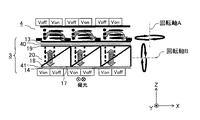
<画像表示装置1の全体構成>
図1Aは、実施の形態に係る画像表示装置1の概略断面図であり、図1Bは、図1Aに示す画像表示装置1の一部の分解斜視図である。尚、図1Aにおいては、図1Bに記載の電極40a、40b、41a、41bの記載が省略されている。
<Overall Configuration of
FIG. 1A is a schematic cross-sectional view of an
本実施の形態では、画像表示装置1に対して3次元直交座標系を設定し、座標軸を用いて方向を特定する。図1A及び1Bに示すように、X軸方向は、画像表示パネル4の表示面に対してユーザが正対したときの左右方向(水平方向)と一致している。Y軸方向は、画像表示パネル4の表示面に対してユーザが正対したときの上下方向に一致している。Z軸方向は、画像表示パネル4の表示面に対して垂直な方向に一致している。ここで、「正対」とは、例えば表示面に「A」という文字が表示されている場合において、ユーザがこの「A」という文字を正しい方向から見るように、表示面の真正面に向かって位置していることを意味する。また、図1A及び1Bは、画像表示装置1の上側から見た図に相当する。したがって、図1A及び1Bの左側が、視聴者から見た表示画面の右側となる。
In the present embodiment, a three-dimensional orthogonal coordinate system is set for the
画像表示装置1は、光源切替型のバックライト2と、液晶プリズム素子3と、右眼用画像及び左眼用画像を交互に切り替えながら表示する画像表示パネル4と、画像表示装置1を使用しているユーザの位置検出を行う位置検出部38と、検出されたユーザの位置情報に基づいて、液晶プリズム素子3へ出力する液晶駆動電圧を制御する制御部6とから構成される。以下、各構成に対してそれぞれ詳細を述べる。
The
<バックライト2の詳細構成>
バックライト2は、互いに対向する光源7a及び7bと、反射フィルム8と、導光板9と、光制御フィルム10とで構成される。反射フィルム8は導光板9の下面側に設けられており、光制御フィルム10は導光板9の上面側に設けられている。
<Detailed configuration of
The
光源7a及び7bは、導光板9の一対の側面のそれぞれに沿って配置されており、X軸方向において互いに対向している。光源7aは、導光板9の左側面に配置されており、光源7bは導光板9の右側面に配置されている。光源7a及び7bは、それぞれY軸方向に配列された複数のLED素子を有している。光源7a及び7bは、画像表示パネル4に表示される左眼用画像及び右眼用画像の切り替えに同期して、交互に点灯及び点滅を繰り返す。すなわち、画像表示パネル4が右眼用画像を表示する場合は、光源7aが点灯して光源7bが消灯し、画像表示パネル4が左眼用画像を表示する場合は、光源7aが消灯して光源7bが点灯する。
The
光源7a及び7bから出射された光は、導光板9の上面と下面とで全反射を繰り返しながら導光板9内に広がる。導光板9内で全反射角度を超える角度を持った光が導光板9の上面から出射される。導光板9の下面は、図1A及び1Bに示すように、複数の傾斜面35により構成されている。これらの傾斜面35により、導光板9内を伝搬する光は様々な方向に反射されるので、導光板9から出射する光の強度が上面全体にわたって均一になる。
Light emitted from the
反射フィルム8は、導光板9の下面側に設けられている。導光板9の下面に設けられた傾斜面35の全反射角度を破った光は、反射フィルム8により反射され、再び導光板9内に入射し、最終的に上面から出射される。導光板9から出射された光は、光制御フィルム10に入射する。
The reflective film 8 is provided on the lower surface side of the light guide plate 9. The light that has broken the total reflection angle of the
光制御フィルム10の下面には、三角形状の断面及びY軸方向に延びる稜線を有する複数のプリズム36が、X軸方向に並列に配置されている。すなわち、光制御フィルム10の下面には、三角形状の断面を有するプリズム36が1次元アレイ配置されている。また、光制御フィルム10の上面には、Y軸方向に延びる複数のシリンドリカルレンズ37がX軸方向に並列に配置されている。すなわち、光制御フィルム10の上面には、レンチキュラーレンズが形成されている。
On the lower surface of the
光制御フィルム10の下面に入射した光は、プリズム36によりZ軸方向に立ち上げられ、上面のレンチキュラーレンズにより集光され、液晶プリズム素子3に入射する。
Light incident on the lower surface of the
<液晶プリズム素子3の詳細構成>
図2は、実施の形態に係る液晶プリズム素子及び画像表示パネルの構成例を示す図である。以下、図1A、1B及び2を併せて参照しながら、液晶プリズム素子3の詳細を説明する。
<Detailed Configuration of Liquid
FIG. 2 is a diagram illustrating a configuration example of the liquid crystal prism element and the image display panel according to the embodiment. Hereinafter, the liquid
液晶プリズム素子3は、左側の光源7aから出射され、導光板9及び光制御フィルム10を通じて入射した光が、ユーザの右眼の位置に集光するように、偏光方向を制御する。また、右側の光源7bから出射され、導光板9及び光制御フィルム10を通じて入射した光が、ユーザの左眼の位置に集光するように、偏光方向を制御する。
The liquid
より詳細には、液晶プリズム素子3は、一対の対向基板13及び14と、対向基板13及び14の間に封入される複数のプリズム17及び液晶層20と、対向基板13の内面に設けられる電極40a及び40bと、対向基板14の内面に設けられる電極41a及び41bとを備える。
More specifically, the liquid
プリズム17は、三角形の断面とY軸方向に延びる稜線とを有する三角柱形状を有する。図1及び2から理解されるように、複数のプリズム17が、電極41a及び41b上にX軸方向に並べて設けられている。複数のプリズム17の断面形状は、左右対称となるように構成されている。説明を容易にするために、プリズム17の形成領域を図1A及び1Bにおける左半分及び右半分に二分し、左側の領域をR1、領域R1とX軸方向に隣接する右側の領域をR2とする。また、領域R1及びR2の境界線(中央線)を通過し、かつ、画像表示パネル4の表示面と直交する平面を、P1とする。XZ平面と平行な平面上で見たときに、領域R1に配置されるプリズム17の断面形状と、領域R2に配置されるプリズム17の断面形状とは、図1A及び1Bに示すように、平面P1に対して対称となるように設計されている。
The
電極40aは、対向基板13の内面の領域R1に形成され、電極40bは、対向基板13の内面の領域R2に形成されている。同様に、電極41aは、対向基板14の内面の領域R1に形成され、電極41bは、対向基板14の内面の領域R2に形成されている。
The
更に、プリズム17の表面上及び電極40a及び40b上には、液晶分子の配向方向を所望の方向に制御するための配向処理を施した配向膜18及び19が設けられている。配向膜18及び19は、電極40a、40b、41a、41bに電圧が印加されていない状態で、液晶分子の長軸がY軸方向となるように液晶分子を配向させる。ただし、液晶分子の配向が均一に保てるのであれば、配向膜18及び19はなくても良い。
Further, on the surface of the
尚、対向基板13及び14、プリズム17の形成材料としては、ガラスまたは樹脂を用いることができる。一例として、ガラス基板上にUV硬化樹脂をインプリントすることによって、プリズム17を形成することができる。液晶プリズム素子3は、電極41a及び41bを成膜した対向基板14上にプリズム17の一次元配列を形成した後、対向基板14と、電極40a及び40bを成膜した対向基板13とを貼り合わせ、対向基板13及び14の間に液晶を封入することによって作製できる。
Note that glass or resin can be used as a material for forming the
液晶プリズム素子3は、外部からの印加電圧の大きさに応じて、透過する光の偏向角度の大きさを制御できる素子である。その原理を簡単に述べる。通常、液晶分子は楕円体形状をしており、長手方向と短手方向とで誘電率が異なる。このため、液晶層20は、入射光の偏光方向毎に屈折率が異なる複屈折の性質を有する。また、液晶分子の配向(ダイレクタ)の向きが光の偏光方向に対して相対的に変化すれば、液晶層20の屈折率も変化する。そのため、ある印加電圧を与えて発生させた電場により液晶の配向を変化させると、透過する光に対する屈折率が変わるため、光の屈折角である偏向角が変化する。
The liquid
一般的に、液晶プリズム素子3等のアクティブ素子で光を偏向させる場合に、偏向角を大きくするためには、Δn(=常光に対する屈折率no−異常光に対する屈折率ne)が大きな液晶材料を用いることが望ましい。しかしながら、市販されている中でΔnが大きな液晶材料は少なく、一般的に、Δnは約0.2程度である。
In general, in order to increase the deflection angle when light is deflected by an active element such as the liquid
また、同じ液晶材料で用いて液晶プリズムを構成しても配向方向の設計、電場のかけ方が液晶プリズム素子の能力である偏向角や、電力や、スイッチングスピードなどといった素子性能を大きく左右する重要な項眼である。本開示では、最適な液晶の初期配向及び配向回転方向をシミュレーションによって導出した。 Even if the liquid crystal prism is composed of the same liquid crystal material, the design of the orientation direction and the way the electric field is applied are important factors that greatly affect the device performance such as the deflection angle, power, switching speed, etc. It is an important item. In the present disclosure, the optimal initial alignment and alignment rotation direction of the liquid crystal are derived by simulation.
図2には、液晶プリズム素子3に電圧を印加した場合の液晶分子の配向(Von)と、電圧を印加していない場合の液晶分子の初期配向(Voff)とが並べて模式的に示されている。電圧が印加されていない場合の初期配向方向は、Y軸方向である。一方電圧が印加された場合は、液晶分子がX軸方向に並ぶ。このように、本実施の形態に係る液晶プリズム素子3では、液晶層20内の液晶分子の配向が変化する際の配向回転軸Bは、X軸と平行、すなわち、画像表示パネル4の表示面と平行で、かつ、画像表示パネル4の左右方向の一辺と平行となる。ただし、プリズム17の斜面上には配向膜19が設けられ、電極40a及び40b上には配向膜18が設けられているため、これらの近傍の液晶分子の配向は、電圧が印加された場合でも変化はない。
FIG. 2 schematically shows the alignment (Von) of the liquid crystal molecules when a voltage is applied to the liquid
尚、液晶プリズム素子3では、プリズム17の斜面の傾斜方向が、画面の中心線(平面P1)を境界にして左右で異なっている。液晶プリズム素子3では、出射光をプリズム17の傾斜面から遠ざける方向(図2における左上方向に相当)への偏向と比べて、出射光をプリズム17の傾斜面に近づける方向(図2における右上方向)への偏向の効率が低いという性質がある。そこで、プリズム17の傾斜面を平面P1に対して対称とし、プリズム17の傾斜面を画面の中央部の前方に向けることによって、液晶プリズム素子3は、画面の左端近傍に入射した光を画面の右前方へと効率的に偏向することができ、画面の右端近傍に入射した光を画面の左前方へと効率的に偏向することができる。この場合、液晶プリズム素子3の左右の領域に異なる電圧が印加される。そのために、電極40a及び40bと、電極41a及び41bとは、画面中央で分離されている。
In the liquid
液晶プリズム素子3を透過した光は、画像表示パネル4に入射する。図2には、印加電圧に応じて回転軸Aを中心に液晶分子が回転する、In−Plane−Switchin
g方式の画像表示パネル4が例示されているが、他の方式の画像表示パネルを採用することもできる。画像表示パネル4を透過した光は、指向性を持ち、視聴者の眼の位置に集光される。
The light transmitted through the liquid
Although the g-type image display panel 4 is illustrated, other types of image display panels may be employed. The light transmitted through the image display panel 4 has directivity and is collected at the position of the viewer's eyes.
画像表示装置1は、右眼用画像と左眼用画像の切り替えに同期させて、光源7a及び7bの切り替えを行っている。また、右眼用画像と左眼用画像との切り替えを120Hz以上の周波数で行うことで、ユーザは右眼用画像と左眼用画像とに基づいて立体画像を認識することができる。
The
<位置検出部38の詳細構成>
位置検出部38は、カメラ5と視聴位置算出部39とを含む。カメラ5は、ユーザの画像を所定周期で撮影する。視聴位置算出部39は、カメラ5によって撮影された画像を解析し、ユーザの視聴位置を表す視聴位置情報を算出する。カメラ5が行う画像解析には、顔や顔の一部(眼や鼻など)の位置を認識する公知のアルゴリズムを利用できる。また、視聴位置算出部39が求める視聴位置情報は、ユーザの目の位置を表すものであることが好ましいが、眼の位置に代えて顔や鼻等の位置を表しても良い。
<Detailed Configuration of
The
制御部6は、視聴位置算出部39によって求められた視聴位置情報に基づいて、液晶プリズム素子3に印加する電圧値を制御する。より詳細には、ユーザの視聴位置が、図1Aに示すように、画面中央から右方向に移動した場合、印加電圧を大きくし、液晶層20の屈折率をプリズム17の屈折率より小さくすることによって、プリズム17からの出射光をユーザから見て右方向に偏向させる。このとき、領域R1への印加電圧を、領域R2への印加電圧より小さくすることによって、領域R1の偏向角と領域R2の偏向角とを揃えることができる。逆に、ユーザの視聴位置が、図1Aに示すように、画面中央から左方向に移動した場合、印加電圧を大きくし、液晶層20の屈折率をプリズム17の屈折率より大きくすることによって、プリズム17からの出射光をユーザから見て左方向に偏向させる。このとき、領域R2への印加電圧を、領域R1への印加電圧より大きくすることによって、領域R1の偏向角と領域R2の偏向角とを揃えることができる。
The
尚、印加電圧に対する液晶プリズム素子3の偏向角及び光の集光点の位置情報は設計段階で想定できるため、予め印加電圧と位置情報とを関連付けたデータを用意し、画像表示装置1が備える記憶装置に格納しておけば良い。また、製品完成後、キャリブレーションを行って、集光点の位置の補正を行っても良い。
The position information of the deflection angle of the liquid
以上で説明した視聴位置情報に基づく偏向制御を所定の周期毎に繰り返し行うことによって、画像表示装置1に対して視聴者が自由に移動した場合でも、任意の場所で、立体画像を視聴することが可能となる。よって、本開示によれば、視域の広い画像表示装置を実現できる。また、光を視聴者の目の位置に集光させることで、高輝度かつ省エネの画像表示装置1を実現できる。
By repeatedly performing the deflection control based on the viewing position information described above at predetermined intervals, a stereoscopic image can be viewed at an arbitrary place even when the viewer freely moves with respect to the
<その他の変形例>
尚、本実施の形態では、導光板9は、光源7a及び7bで共用されているが、光源7a用の導光板と光源7b用の導光板とを設け、2枚の導光板を重ねて配置しても良い。
<Other variations>
In this embodiment, the light guide plate 9 is shared by the
また、プリズムとレンチキュラーレンズとが一体になった制御フィルム10に代えて、プリズムシート及びレンチキュラーレンズシートを別個に設けても良い。
Further, instead of the
更に、バックライト2は、図1A及び1Bに記載された構成に限定されず、左右の画像信号の切り替えと同期して、右眼用の光と左眼用の光とを時分割で交互に出射できるものであれば、他の構成を採用しても良い。
Furthermore, the
更に、本実施の形態では、液晶プリズム素子3内のプリズム17の傾斜面の向きを領域R1及びR2で異ならせ、平面P1に対して対称となるように構成しているが、プリズムの傾斜面の向きを液晶プリズム素子3全体で一定としても良い。この場合、本実施の形態のように、液晶プリズム素子3の領域R1及びR2で電極を分ける代わりに、表示画面全領域にわたって、1つの電極を設ける。しかしながら、配向変化に対する光線の偏向角及び透過効率の面で、2つの領域R1及びR2に分けてプリズム17及び電極を設けることがより好ましい。
Furthermore, in the present embodiment, the direction of the inclined surface of the
更に、本実施の形態では、視差のある右眼用画像及び左眼用画像を時分割で表示する立体画像表示装置を例として説明したが、視差のない画像を表示しても良い。この場合、光源7a及び7bを交互に点滅させる代わりに、常時点灯させる。3次元画像に限らず、二次元画像を表示する際にも、視聴者の動きに追従して、視聴者の眼付近にのみ画像を縮小投影させることにより、省エネだけでなく、周辺の人から表示されている内容を覗かれることも防止でき、プライバシー保護も向上できる。
Furthermore, in the present embodiment, a stereoscopic image display device that displays a right-eye image and a left-eye image with parallax in a time-division manner is described as an example, but an image without parallax may be displayed. In this case, the
更に、本実施の形態では、画像表示パネルとバックライト装置との間に配置され、入射光を偏向させる第1の光学素子として、液晶プリズム素子3内のプリズム17を用い、画像表示パネルとバックライト装置との間に配置され、印加される電圧に応じて屈折率を変化させることにより出射光の偏向方向を変化させる第2の光学素子として、液晶プリズム素子内の液晶素子を用いている。ただし、プリズム17等の光学素子と、液晶素子とは、必ずしも液晶プリズム素子として一体化されている必要はなく、それぞれを分離して設けても良い。また、第1の光学素子は、必ずしもプリズムである必要はなく、レンチキュラーレンズや液晶素子でも良い。
Furthermore, in the present embodiment, the
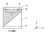
(実施例1)
図3は、実施例1に係る液晶プリズム素子の構成を示す図である。実施例1に係る液晶プリズム素子3は、対向基板13及び14の内面に電極40及び41が形成され、電圧印加時に厚み方向に電界Eを生じる構成である。
Example 1
FIG. 3 is a diagram illustrating the configuration of the liquid crystal prism element according to the first embodiment. The liquid
図4は、図3に示す液晶プリズム素子に関するダイレクタの計算結果を示す図である。より詳細には、図4(a)、4(b)、4(c)は、それぞれ、印加電圧が0V、10V、20Vのときの液晶分子の配向分布(ダイレクタ)を示す。 FIG. 4 is a diagram illustrating a director calculation result regarding the liquid crystal prism element illustrated in FIG. 3. More specifically, FIGS. 4A, 4B, and 4C show the orientation distribution (director) of liquid crystal molecules when the applied voltage is 0V, 10V, and 20V, respectively.
図4(a)に示すように、印加電圧が0Vの状態、すなわち、初期状態では、液晶分子は図4の紙面に垂直な方向(図3のY軸方向)に配向している。次に、10Vまたは20Vの電圧を印加すると、図4(b)及び4(c)に示すように、液晶分子が回転して配向状態が変化する。図4(b)に示す状態と比べて、図4(c)に示す状態では、液晶層20のより広い範囲で液晶分子の配向を変化させることができる。したがって、印加電圧を大きくするほど、透過光に対する屈折率を大きくすることができ、この結果、偏向角を大きくすることができる。
As shown in FIG. 4A, in the state where the applied voltage is 0 V, that is, in the initial state, the liquid crystal molecules are aligned in a direction perpendicular to the paper surface of FIG. 4 (Y-axis direction of FIG. 3). Next, when a voltage of 10 V or 20 V is applied, as shown in FIGS. 4B and 4C, the liquid crystal molecules rotate and the alignment state changes. Compared with the state shown in FIG. 4B, in the state shown in FIG. 4C, the orientation of the liquid crystal molecules can be changed in a wider range of the
(比較例1)
図5は、比較例1に係る液晶プリズム素子の構成を示す図である。比較例1に係る液晶プリズム素子は、実施例1と同一の対向基板13及び14、プリズム17、液晶層20を備えるが、基板13の内面に一対の電極42及び43が形成され、電圧印加時に液晶プリズム素子の平面方向(図5の左右方向)に電界E’を生じる点で実施例1と異なる。
(Comparative Example 1)
FIG. 5 is a diagram illustrating a configuration of the liquid crystal prism element according to the first comparative example. The liquid crystal prism element according to Comparative Example 1 includes the
図6は、比較例1に係る液晶プリズム素子に関するダイレクタの計算結果を示す図であ
る。より詳細には、図6(a)、6(b)、6(c)は、それぞれ、印加電圧が0V、10V、50Vのときの液晶分子の配向分布(ダイレクタ)を示す。
FIG. 6 is a diagram illustrating a calculation result of a director related to the liquid crystal prism element according to the first comparative example. More specifically, FIGS. 6 (a), 6 (b), and 6 (c) show alignment distributions (directors) of liquid crystal molecules when applied voltages are 0V, 10V, and 50V, respectively.
実施例1と同様に、印加電圧が0Vの状態、すなわち、初期状態では、液晶分子は図6(a)に示すように、紙面に垂直な方向(図5のY軸方向)に配向している。次に、10Vまたは50Vの電圧を印加すると、図6(b)及び6(c)に示すように、液晶分子が回転して配向状態が変化する。このとき、液晶分子は、その長軸が電界E’の向きに沿うように配向するが、液晶層20のうち、電極から離れた部分(破線で囲んだ部分)には、十分な電界が生じないため、液晶の配向が十分に変化していない。したがって、図5に示す比較例1の構成では、液晶層の屈折率変化を大きくすることが難しく、それ故、偏向角を大きくすることができない。
As in Example 1, in the state where the applied voltage is 0 V, that is, in the initial state, the liquid crystal molecules are aligned in a direction perpendicular to the paper surface (Y-axis direction in FIG. 5) as shown in FIG. Yes. Next, when a voltage of 10 V or 50 V is applied, as shown in FIGS. 6B and 6C, the liquid crystal molecules rotate and the alignment state changes. At this time, the liquid crystal molecules are aligned such that the major axis thereof is along the direction of the electric field E ′, but a sufficient electric field is generated in a portion of the
(実施例2)
図7は、実施例2に係る液晶プリズム素子の構成を示す図である。図7に示す液晶プリズム素子は、対向基板27及び28と、対向基板27の内面に設けられた電極29と、対向基板28の内面に設けられた電極30と、電極30上に形成されたプリズム32と、プリズム32と対向基板27との間に封入された液晶層31と、プリズム32の表面に設けられた配向膜33と、電極29の表面に設けられた配向膜34とを備える。
(Example 2)
FIG. 7 is a diagram illustrating the configuration of the liquid crystal prism element according to the second embodiment. The liquid crystal prism element shown in FIG. 7 includes
図8は、実施例2に係る液晶プリズム素子構成に関する屈折率の計算結果を示す図である。より詳細には、図8(a)は、図7のA−A’線上の位置と当該位置での液晶層の屈折率との関係を、電圧を様々に変えてシミュレーションした結果を示し、図8(b)は、液晶分子の配向方向を図2と同様の記載方法で記載したものである。 FIG. 8 is a diagram illustrating a calculation result of the refractive index regarding the configuration of the liquid crystal prism element according to the second embodiment. More specifically, FIG. 8A shows the result of simulating the relationship between the position on the AA ′ line in FIG. 7 and the refractive index of the liquid crystal layer at the position by varying the voltage. 8 (b) describes the orientation direction of the liquid crystal molecules by the same description method as in FIG.
実施例2では、図8(b)に示すように、印加電圧が0Vの初期状態では、液晶分子が対向基板27及びプリズム32の斜面の両方に対して平行で、かつ、紙面と直交する方向に配向されるように配向膜33及び34に配向処理が施されている。
In Example 2, as shown in FIG. 8B, in the initial state where the applied voltage is 0 V, the liquid crystal molecules are parallel to both the
図8(a)に示すように、プリズム32の材料屈折率は1.6であり、液晶層の屈折率は印加電圧に応じて変化している。印加電圧が0V及び100Vのときに、プリズムの材料屈折率との差が大きくなり、透過光に対する偏向角を大きくすることができる。
As shown in FIG. 8A, the material refractive index of the
(比較例2及び3)
図9及び10は、比較例2及び3に係る液晶プリズム素子構成に関する屈折率の計算結果を示す図である。より詳細には、図9(a)及び10(a)は、図7のA−A’線上の位置と当該位置での液晶層の屈折率との関係を、電圧を様々に変えてシミュレーションした結果を示し、図9(b)及び10(b)は、液晶分子の配向方向を図2と同様の記載方法で記載したものである。
(Comparative Examples 2 and 3)
FIGS. 9 and 10 are diagrams showing the calculation results of the refractive index regarding the liquid crystal prism element configuration according to Comparative Examples 2 and 3. FIGS. More specifically, FIGS. 9A and 10A simulate the relationship between the position on the line AA ′ in FIG. 7 and the refractive index of the liquid crystal layer at that position by varying the voltage. The results are shown, and FIGS. 9B and 10B show the orientation directions of the liquid crystal molecules in the same way as in FIG.
比較例2に係る液晶プリズムの基本的な構成は、図7に示した実施例2と同じであるが、配向膜33及び34に代えて、配向膜23及び24を備える点で実施例2と異なる。具体的には、図9(b)に示すように、配向膜24は、液晶分子を対向基板27に対して平行で、かつ、紙面の左右方向に配向させる。配向膜23は、液晶分子をプリズム32の斜面に対して垂直に配向させる。
The basic configuration of the liquid crystal prism according to Comparative Example 2 is the same as that of Example 2 shown in FIG. 7, but is different from Example 2 in that
図9(a)に示すように、印加電圧が0Vの初期状態において、プリズム32の斜面近傍の液晶層の屈折率は約1.65であるが、対向基板27近傍の液晶層の屈折率は約1.7である。したがって、印加電圧が0Vのときにおける液晶層31による偏向角は、実施例2と比べて小さくなる。
As shown in FIG. 9A, in the initial state where the applied voltage is 0 V, the refractive index of the liquid crystal layer near the inclined surface of the
比較例3に係る液晶プリズムの基本的な構成は、図7に示した実施例2と同じであるが、配向膜33及び34に代えて、配向膜25及び26を備える点で実施例2と異なる。具体的には、配向膜26は、図10(b)に示すように、液晶分子を対向基板27に対して平行で、かつ、紙面の左右方向に配向させる。配向膜25は、液晶分子をプリズム32の斜面に対して平行で、かつ、紙面と平行な方向に配向させる。
The basic configuration of the liquid crystal prism according to Comparative Example 3 is the same as that of Example 2 shown in FIG. 7, but is different from Example 2 in that
図10(a)に示すように、印加電圧が0Vの初期状態において、プリズム32の斜面近傍の液晶層の屈折率は約1.525であるが、対向基板27近傍の液晶層の屈折率は約1.7である。したがって、印加電圧が0Vのときにおける液晶層31による偏向角は、実施例2と比べて小さくなる。
As shown in FIG. 10A, in the initial state where the applied voltage is 0 V, the refractive index of the liquid crystal layer near the slope of the
実施例2と比較例2及び3との対比から、印加電圧が0Vの初期状態において、液晶プリズムの稜線方向(図7のY軸方向)に液晶分子を配向させ、配向回転軸をプリズム32の稜線と直交させた場合に、最も偏向角を大きくできることが確認された。 From the comparison between Example 2 and Comparative Examples 2 and 3, in the initial state where the applied voltage is 0 V, the liquid crystal molecules are aligned in the ridge line direction of the liquid crystal prism (Y-axis direction in FIG. 7), and the rotation axis of the alignment is It was confirmed that the deflection angle can be maximized when it is orthogonal to the ridgeline.
以上のように、本開示における技術の例示として、実施の形態及び実施例を説明した。そのために、添付図面および詳細な説明を提供した。 As described above, the embodiments and examples have been described as examples of the technology in the present disclosure. For this purpose, the accompanying drawings and detailed description are provided.
したがって、添付図面および詳細な説明に記載された構成要素の中には、課題解決のために必須な構成要素だけでなく、上記技術を例示するために、課題解決のためには必須でない構成要素も含まれ得る。そのため、それらの必須ではない構成要素が添付図面や詳細な説明に記載されていることをもって、直ちに、それらの必須ではない構成要素が必須であるとの認定をするべきではない。 Accordingly, among the components described in the accompanying drawings and the detailed description, not only the components essential for solving the problem, but also the components not essential for solving the problem in order to illustrate the above technique. May also be included. Therefore, it should not be immediately recognized that these non-essential components are essential as those non-essential components are described in the accompanying drawings and detailed description.
また、上述の実施の形態は、本開示における技術を例示するためのものであるから、特許請求の範囲またはその均等の範囲において種々の変更、置き換え、付加、省略などを行うことができる。 Moreover, since the above-mentioned embodiment is for demonstrating the technique in this indication, a various change, replacement, addition, abbreviation, etc. can be performed in a claim or its equivalent range.
本開示は、高輝度、高効率、高解像度の画像表示装置に適用できる。また、本開示は、3次元画像の表示用途だけでなく、2次元画像の表示用途にも広く適用することができる。具体的には、本開示は、3D液晶表示装置やプライバシーディスプレイ等に適用することが可能である。 The present disclosure can be applied to an image display device with high brightness, high efficiency, and high resolution. In addition, the present disclosure can be widely applied not only to a display application of a three-dimensional image but also to a display application of a two-dimensional image. Specifically, the present disclosure can be applied to a 3D liquid crystal display device, a privacy display, and the like.
1 画像表示装置
2 バックライト
3 液晶プリズム素子
4 画像表示パネル
5 カメラ
6 制御部
7a、7b 光源
8 反射フィルム
9 導光板
10 光制御フィルム
13、28 対向基板
14、27 対向基板
17、32 プリズム
18、19、23、24、25、26、33、34 配向膜
20、31 液晶層
DESCRIPTION OF
Claims (3)
前記第1の光学素子及び前記第2の光学素子は液晶プリズム素子を構成し、
前記液晶プリズム素子において、第1の光学素子は、一対の対向基板の間に配置され、かつ三角形状の断面及び前記画像表示パネルの一辺と平行な第1の方向に延びる稜線を有する複数のプリズムが、前記第1の方向と直交する第2の方向に並列に配置されることにより構成され、
前記液晶プリズム素子において、第2の光学素子は、前記複数のプリズムと前記対向基板の一方との間に形成される液晶層と、前記対向基板の各々の内面に設けられる電極とを含み、電圧が印加されたときに厚み方向の電界を発生させる液晶素子により構成され、
さらに前記液晶プリズム素子は、前記第2の方向に隣接する第1の領域及び第2の領域に区分し、前記第1の領域に配置される前記プリズムの断面形状と、前記第2の領域に配置される前記プリズムの断面形状は、前記画像表示パネルの表示面と直交し、第1の領域及び第2の領域の境界を通過する平面に対して対称となるように構成した画像表示装置。 An image display panel; a backlight device disposed on a back side of the image display panel; a first optical element disposed between the image display panel and the backlight device and deflecting incident light; A second optical element that is arranged between the image display panel and the backlight device and changes the deflection direction of the emitted light by changing the refractive index according to the applied voltage, and detects the position of the user A position detection unit, and a control unit that controls a voltage applied to the second optical element based on user position information detected by the position detection unit,
It said first optical element and the second optical element is a liquid crystal prism element,
In the liquid crystal prism element, the first optical element is disposed between a pair of opposing substrates, and has a plurality of prisms having a triangular cross section and a ridge line extending in a first direction parallel to one side of the image display panel. Is arranged in parallel in a second direction orthogonal to the first direction,
In the liquid crystal prism element, the second optical element includes a liquid crystal layer formed between the plurality of prisms and one of the counter substrates, and an electrode provided on each inner surface of the counter substrate, and a voltage Is formed by a liquid crystal element that generates an electric field in the thickness direction when applied,
Further, the liquid crystal prism element is divided into a first region and a second region adjacent to each other in the second direction, and the cross-sectional shape of the prism disposed in the first region and the second region An image display device configured such that a cross-sectional shape of the arranged prism is orthogonal to a display surface of the image display panel and is symmetric with respect to a plane passing through a boundary between the first region and the second region.
Priority Applications (1)
| Application Number | Priority Date | Filing Date | Title |
|---|---|---|---|
| JP2013544118A JP5828092B2 (en) | 2011-11-16 | 2012-11-12 | Image display device |
Applications Claiming Priority (4)
| Application Number | Priority Date | Filing Date | Title |
|---|---|---|---|
| JP2011251121 | 2011-11-16 | ||
| JP2011251121 | 2011-11-16 | ||
| JP2013544118A JP5828092B2 (en) | 2011-11-16 | 2012-11-12 | Image display device |
| PCT/JP2012/007224 WO2013073147A1 (en) | 2011-11-16 | 2012-11-12 | Image display device |
Publications (2)
| Publication Number | Publication Date |
|---|---|
| JPWO2013073147A1 JPWO2013073147A1 (en) | 2015-04-02 |
| JP5828092B2 true JP5828092B2 (en) | 2015-12-02 |
Family
ID=48429245
Family Applications (1)
| Application Number | Title | Priority Date | Filing Date |
|---|---|---|---|
| JP2013544118A Expired - Fee Related JP5828092B2 (en) | 2011-11-16 | 2012-11-12 | Image display device |
Country Status (3)
| Country | Link |
|---|---|
| US (1) | US9405125B2 (en) |
| JP (1) | JP5828092B2 (en) |
| WO (1) | WO2013073147A1 (en) |
Families Citing this family (8)
| Publication number | Priority date | Publication date | Assignee | Title |
|---|---|---|---|---|
| US9497444B2 (en) * | 2012-10-03 | 2016-11-15 | Sharp Kabushiki Kaisha | Stereoscopic display device |
| KR102197536B1 (en) * | 2014-08-18 | 2020-12-31 | 엘지디스플레이 주식회사 | 3d display device for reducing moving flicker |
| CN104391378A (en) * | 2014-11-21 | 2015-03-04 | 苏州福丰科技有限公司 | Two-dimensional and three-dimensional mode switchable watch device |
| KR20160087185A (en) * | 2015-01-13 | 2016-07-21 | 한국전자통신연구원 | Back light unit and display device |
| US9898076B1 (en) * | 2015-02-02 | 2018-02-20 | Amazon Technologies, Inc. | Adjusting electronic displays based on user viewing position |
| CN105549266B (en) * | 2016-03-03 | 2019-12-10 | 京东方科技集团股份有限公司 | Liquid crystal display |
| CN105511179B (en) * | 2016-03-03 | 2020-02-18 | 京东方科技集团股份有限公司 | Liquid crystal display |
| CN116088193A (en) * | 2022-11-07 | 2023-05-09 | 北京京东方技术开发有限公司 | Display device |
Family Cites Families (15)
| Publication number | Priority date | Publication date | Assignee | Title |
|---|---|---|---|---|
| JPH0798439A (en) * | 1993-09-29 | 1995-04-11 | Nippon Telegr & Teleph Corp <Ntt> | Three-dimensional stereoscopic display device |
| JPH0918897A (en) * | 1995-07-03 | 1997-01-17 | Canon Inc | Stereoscopic image display device |
| JPH11234705A (en) * | 1998-02-17 | 1999-08-27 | Matsushita Electric Ind Co Ltd | Stereoscopic display device |
| US6169594B1 (en) | 1998-08-24 | 2001-01-02 | Physical Optics Corporation | Beam deflector and scanner |
| CN100376924C (en) * | 2002-09-19 | 2008-03-26 | 三菱电机株式会社 | Display unit and electronic apparatus equipped with display unit |
| JP2006293106A (en) | 2005-04-12 | 2006-10-26 | Toshiba Corp | Stereoscopic display device |
| US20110090413A1 (en) * | 2006-08-18 | 2011-04-21 | Industrial Technology Research Institute | 3-dimensional image display |
| JP2010507823A (en) * | 2006-10-26 | 2010-03-11 | シーリアル テクノロジーズ ソシエテ アノニム | Small holographic display device |
| JP5191491B2 (en) | 2006-10-26 | 2013-05-08 | シーリアル テクノロジーズ ソシエテ アノニム | Small holographic display device |
| DE102007026071A1 (en) * | 2007-05-24 | 2008-11-27 | Seereal Technologies S.A. | Direction-controlled lighting unit for an autostereoscopic display |
| JP2008310259A (en) * | 2007-06-18 | 2008-12-25 | Sumitomo Chemical Co Ltd | Optical path deflecting plate, surface light source apparatus and transmission type image display apparatus |
| JP5379053B2 (en) * | 2010-03-26 | 2013-12-25 | スタンレー電気株式会社 | Optical deflection device |
| US9201187B2 (en) * | 2010-11-17 | 2015-12-01 | Panasonic Intellectual Property Management Co., Ltd. | Light-emitting device, and liquid crystal display device and image display device that use the same |
| US8988336B2 (en) * | 2010-12-16 | 2015-03-24 | 3M Innovative Properties Company | Dual-orientation autostereoscopic backlight and display |
| US20130107340A1 (en) * | 2011-10-31 | 2013-05-02 | Yoon Kean Wong | Autostereoscopic Steering Light-Guide Three-Dimensional Displays |
-
2012
- 2012-11-12 WO PCT/JP2012/007224 patent/WO2013073147A1/en active Application Filing
- 2012-11-12 JP JP2013544118A patent/JP5828092B2/en not_active Expired - Fee Related
-
2014
- 2014-05-13 US US14/276,828 patent/US9405125B2/en active Active
Also Published As
| Publication number | Publication date |
|---|---|
| WO2013073147A1 (en) | 2013-05-23 |
| JPWO2013073147A1 (en) | 2015-04-02 |
| US9405125B2 (en) | 2016-08-02 |
| US20140247211A1 (en) | 2014-09-04 |
Similar Documents
| Publication | Publication Date | Title |
|---|---|---|
| JP5828092B2 (en) | Image display device | |
| JP5581307B2 (en) | Image display device | |
| JP5620420B2 (en) | Image display device | |
| KR101122199B1 (en) | 2D-3D switchable autostereoscopic display apparatus | |
| US9958692B2 (en) | Multiview display device | |
| JP2013137454A5 (en) | ||
| JP6176546B2 (en) | Image display device | |
| JP5938720B2 (en) | Optical deflection element and image display apparatus using the same | |
| WO2013161257A1 (en) | Liquid crystal optical element and image display device provided therewith | |
| US9030643B2 (en) | Liquid crystal optical element and image display apparatus including the same | |
| CN110012285B (en) | Multi-view stereoscopic display device | |
| JP5942150B2 (en) | Image display device | |
| JP5919510B2 (en) | Image display device | |
| JP5938647B2 (en) | Image display device | |
| JP5591783B2 (en) | Image display device |
Legal Events
| Date | Code | Title | Description |
|---|---|---|---|
| A131 | Notification of reasons for refusal |
Free format text: JAPANESE INTERMEDIATE CODE: A131 Effective date: 20150218 |
|
| A521 | Request for written amendment filed |
Free format text: JAPANESE INTERMEDIATE CODE: A523 Effective date: 20150324 |
|
| TRDD | Decision of grant or rejection written | ||
| A01 | Written decision to grant a patent or to grant a registration (utility model) |
Free format text: JAPANESE INTERMEDIATE CODE: A01 Effective date: 20150423 |
|
| A61 | First payment of annual fees (during grant procedure) |
Free format text: JAPANESE INTERMEDIATE CODE: A61 Effective date: 20150520 |
|
| R151 | Written notification of patent or utility model registration |
Ref document number: 5828092 Country of ref document: JP Free format text: JAPANESE INTERMEDIATE CODE: R151 |
|
| LAPS | Cancellation because of no payment of annual fees |