JP5777300B2 - Driving circuit and display device - Google Patents
Driving circuit and display device Download PDFInfo
- Publication number
- JP5777300B2 JP5777300B2 JP2010152957A JP2010152957A JP5777300B2 JP 5777300 B2 JP5777300 B2 JP 5777300B2 JP 2010152957 A JP2010152957 A JP 2010152957A JP 2010152957 A JP2010152957 A JP 2010152957A JP 5777300 B2 JP5777300 B2 JP 5777300B2
- Authority
- JP
- Japan
- Prior art keywords
- voltage
- power supply
- operational amplifier
- supply voltage
- line
- Prior art date
- Legal status (The legal status is an assumption and is not a legal conclusion. Google has not performed a legal analysis and makes no representation as to the accuracy of the status listed.)
- Active
Links
Images


Classifications
-
- G—PHYSICS
- G09—EDUCATION; CRYPTOGRAPHY; DISPLAY; ADVERTISING; SEALS
- G09G—ARRANGEMENTS OR CIRCUITS FOR CONTROL OF INDICATING DEVICES USING STATIC MEANS TO PRESENT VARIABLE INFORMATION
- G09G3/00—Control arrangements or circuits, of interest only in connection with visual indicators other than cathode-ray tubes
- G09G3/20—Control arrangements or circuits, of interest only in connection with visual indicators other than cathode-ray tubes for presentation of an assembly of a number of characters, e.g. a page, by composing the assembly by combination of individual elements arranged in a matrix no fixed position being assigned to or needed to be assigned to the individual characters or partial characters
- G09G3/34—Control arrangements or circuits, of interest only in connection with visual indicators other than cathode-ray tubes for presentation of an assembly of a number of characters, e.g. a page, by composing the assembly by combination of individual elements arranged in a matrix no fixed position being assigned to or needed to be assigned to the individual characters or partial characters by control of light from an independent source
- G09G3/36—Control arrangements or circuits, of interest only in connection with visual indicators other than cathode-ray tubes for presentation of an assembly of a number of characters, e.g. a page, by composing the assembly by combination of individual elements arranged in a matrix no fixed position being assigned to or needed to be assigned to the individual characters or partial characters by control of light from an independent source using liquid crystals
- G09G3/3611—Control of matrices with row and column drivers
- G09G3/3614—Control of polarity reversal in general
-
- G—PHYSICS
- G09—EDUCATION; CRYPTOGRAPHY; DISPLAY; ADVERTISING; SEALS
- G09G—ARRANGEMENTS OR CIRCUITS FOR CONTROL OF INDICATING DEVICES USING STATIC MEANS TO PRESENT VARIABLE INFORMATION
- G09G3/00—Control arrangements or circuits, of interest only in connection with visual indicators other than cathode-ray tubes
- G09G3/20—Control arrangements or circuits, of interest only in connection with visual indicators other than cathode-ray tubes for presentation of an assembly of a number of characters, e.g. a page, by composing the assembly by combination of individual elements arranged in a matrix no fixed position being assigned to or needed to be assigned to the individual characters or partial characters
- G09G3/34—Control arrangements or circuits, of interest only in connection with visual indicators other than cathode-ray tubes for presentation of an assembly of a number of characters, e.g. a page, by composing the assembly by combination of individual elements arranged in a matrix no fixed position being assigned to or needed to be assigned to the individual characters or partial characters by control of light from an independent source
- G09G3/36—Control arrangements or circuits, of interest only in connection with visual indicators other than cathode-ray tubes for presentation of an assembly of a number of characters, e.g. a page, by composing the assembly by combination of individual elements arranged in a matrix no fixed position being assigned to or needed to be assigned to the individual characters or partial characters by control of light from an independent source using liquid crystals
- G09G3/3611—Control of matrices with row and column drivers
- G09G3/3685—Details of drivers for data electrodes
- G09G3/3688—Details of drivers for data electrodes suitable for active matrices only
Landscapes
- Engineering & Computer Science (AREA)
- Chemical & Material Sciences (AREA)
- Crystallography & Structural Chemistry (AREA)
- Physics & Mathematics (AREA)
- Computer Hardware Design (AREA)
- General Physics & Mathematics (AREA)
- Theoretical Computer Science (AREA)
- Liquid Crystal Display Device Control (AREA)
- Control Of Indicators Other Than Cathode Ray Tubes (AREA)
- Electronic Switches (AREA)
- Amplifiers (AREA)
- Liquid Crystal (AREA)
Description
本発明は、液晶表示パネルなどの表示パネルを駆動する駆動回路及び表示装置に関し、特に、反転駆動方式で動作して表示パネルを駆動する駆動回路及び表示装置に関する。 The present invention relates to a drive circuit and a display device that drive a display panel such as a liquid crystal display panel, and more particularly to a drive circuit and a display device that operate by an inversion drive method to drive a display panel.
アクティブマトリクス型の液晶表示パネルは、一般に、マトリクス状に配列された複数の表示画素を有し、各表示画素が、液晶層と、この液晶層への電界印加を制御するTFT(Thin−Film Transistor:薄膜トランジスタ)などの能動素子とを有する。駆動回路は、各能動素子をオン状態またはオフ状態にする制御信号を走査線(ゲート線)を介して供給するゲートドライバと、各表示画素の液晶層を挟み込む一対の画素電極及び対向電極間にデータ線(ソース線)を介してアナログ階調電圧を印加するソースドライバとを有する。同一極性の直流電圧成分を含む階調電圧を印加し続けると液晶層は劣化するので、画像信号のフレーム表示期間ごとあるいはフィールド表示期間ごとに階調電圧の直流電圧成分の極性を反転させて交流電圧を印加する反転駆動方式が広く採用されている。反転駆動方式により、液晶層に印加される電界の方向が表示期間(たとえば、フレーム期間あるいはフィールド期間)ごとに反転するので、液晶層の劣化を防止することができる。たとえば、ドット(たとえば1画素)単位で正極性の階調電圧(正極性の直流電圧成分を含む階調電圧)と負極性の階調電圧(負極性の直流電圧成分を含む階調電圧)とを交互に印加する反転駆動方式は、ドット反転方式と呼ばれており、走査線単位またはデータ線単位で正極性の階調電圧と負極性の階調電圧とを交互に供給する反転駆動方式は、ライン反転方式と呼ばれている。 An active matrix type liquid crystal display panel generally has a plurality of display pixels arranged in a matrix. Each display pixel has a liquid crystal layer and a TFT (Thin-Film Transistor) that controls electric field application to the liquid crystal layer. A thin film transistor). The driving circuit includes a gate driver that supplies a control signal for turning on or off each active element via a scanning line (gate line), and a pair of pixel electrodes and a counter electrode that sandwich the liquid crystal layer of each display pixel. A source driver that applies an analog gradation voltage via a data line (source line). Since the liquid crystal layer deteriorates when a gradation voltage containing a DC voltage component of the same polarity is applied continuously, the polarity of the DC voltage component of the gradation voltage is inverted every frame display period or field display period of the image signal. An inversion driving method for applying a voltage is widely adopted. By the inversion driving method, the direction of the electric field applied to the liquid crystal layer is inverted every display period (for example, a frame period or a field period), so that deterioration of the liquid crystal layer can be prevented. For example, a positive gradation voltage (a gradation voltage including a positive DC voltage component) and a negative gradation voltage (a gradation voltage including a negative DC voltage component) in units of dots (for example, one pixel), The inversion driving method for alternately applying the voltage is called the dot inversion method, and the inversion driving method for alternately supplying a positive gradation voltage and a negative gradation voltage in units of scanning lines or data lines is used. This is called the line inversion method.
ソースドライバを用いて反転駆動方式を実現する場合、一般に、ソースドライバは、正極性のアナログ階調電圧を出力するオペアンプ(以下「高圧側オペアンプ」と呼ぶ。)と、負極性のアナログ階調電圧を出力するオペアンプ(以下「低圧側オペアンプ」と呼ぶ。)とを含むインピーダンス変換回路を有している。このようなインピーダンス変換回路を有するソースドライバは、たとえば、特開2006−292807号公報(特許文献1)、特開平10−062744号公報(特許文献2)及び特開2005−266738号公報(特許文献3)に開示されている。 When the inversion driving method is realized using a source driver, the source driver generally has an operational amplifier (hereinafter referred to as “high-voltage side operational amplifier”) that outputs a positive analog gradation voltage and a negative analog gradation voltage. An impedance conversion circuit including an operational amplifier (hereinafter referred to as a “low-voltage side operational amplifier”). Source drivers having such an impedance conversion circuit are disclosed in, for example, Japanese Patent Application Laid-Open No. 2006-292807 (Patent Document 1), Japanese Patent Application Laid-Open No. 10-062744 (Patent Document 2) and Japanese Patent Application Laid-Open No. 2005-266738 (Patent Document). 3).
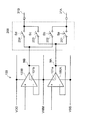
以下、図1を参照しつつ反転駆動方式で動作するソースドライバの問題点を説明する。図1は、ソースドライバにおける低圧側オペアンプ100A及び高圧側オペアンプ100Bを含むインピーダンス変換回路100の一部を概略的に示す図である。低圧側オペアンプ100Aは、電源電圧VSSとこの電源電圧VSSよりも高い共通電源電圧VMMとを用いて動作する非反転増幅器であり、高圧側オペアンプ100Bは、共通電源電圧VMMとこの共通電源電圧VMMよりも高い電源電圧VDDとを用いて動作する非反転増幅器である。低圧側オペアンプ100Aは、低電圧(負極性)のアナログ階調電圧を出力端子NAから出力し、高圧側オペアンプ100Bは、高電圧(正極性)のアナログ階調電圧を出力端子NBから出力する。
Hereinafter, the problem of the source driver operating in the inversion driving method will be described with reference to FIG. FIG. 1 is a diagram schematically showing a part of an
図1に示されるように、低圧側オペアンプ100Aの出力端子NAと高圧側オペアンプ100Bの出力端子NBとは、スイッチ回路200を介してデータ線31A,31Bと接続されている。スイッチ回路200は、切替制御信号Sa,Sb,Sc,Sdに応じて開閉動作するスイッチ201,202,203,204を有している。スイッチ201,204がオン状態のときは、スイッチ202,203はオフ状態となり、スイッチ201,204がオフ状態のときは、スイッチ202,203はオン状態となるように切替制御が行われる。
As shown in FIG. 1, the output terminal NA of the low-voltage
ある画像表示期間Ti(たとえば、フレーム期間またはフィールド期間)から次の画像表示期間Ti+1に移行する際、スイッチ201,204はオン状態からオフ状態に切り替えられ、スイッチ202,203はオフ状態からオン状態に切り替えられる。この際、負極性のアナログ階調電圧が供給されていた低電位のデータ線31Aがオン状態のスイッチ202を介して出力端子NBと接続されるので、出力端子NAの電位が一時的に上昇して出力端子NAが共通電源電圧VMMを上回ることがある。同時に、正極性のアナログ階調電圧が供給されていた高電位のデータ線31Bがオン状態のスイッチ203を介して出力端子NAと接続されるので、出力端子NBの電位が一時的に下降して共通電源電圧VMMを下回ることがある。このような場合、低圧側オペアンプ100A及び高圧側オペアンプ100Bの内部に形成されている寄生ダイオード101a,101bに順方向バイアスが印加されて過電流が流れることにより、低圧側オペアンプ100A及び高圧側オペアンプ100Bが破壊されるおそれがある。
When shifting from one image display period T i (for example, a frame period or a field period) to the next image display period T i + 1 , the
上記に鑑みて本発明の目的は、高圧側オペアンプ及び低圧側オペアンプのいずれかに過電流が発生することを防止することができる駆動回路及び表示装置を提供することである。 In view of the above, an object of the present invention is to provide a drive circuit and a display device that can prevent an overcurrent from occurring in either a high-voltage operational amplifier or a low-voltage operational amplifier.
本発明の第1の駆動回路は、複数の信号線と、前記複数の信号線と離間して交差するように配列された複数のデータ線と、前記信号線と前記データ線との交差点付近の領域にそれぞれ形成された容量性負荷とを有する表示パネルを駆動する駆動回路であって、第1電源電圧と該第1電源電圧よりも低い第2電源電圧とを用いて動作して正極性の直流電圧成分を有するアナログ電圧を出力する第1のオペアンプと、第3電源電圧と該第3電源電圧よりも低い第4電源電圧とを用いて動作して負極性の直流電圧成分を有するアナログ電圧を出力する第2のオペアンプと、前記第1のオペアンプの出力端子の接続先を前記複数のデータ線のうちの第1のデータ線から該第1のデータ線とは異なる第2のデータ線へ切り替えると同時に、前記第2のオペアンプの出力端子の接続先を前記第2のデータ線から前記第1のデータ線に切り替えるスイッチ回路と、を備え、前記第1のオペアンプは、前記第1のオペアンプにおいて形成された、前記第2電源電圧を供給する電源ラインに接続されたアノードと前記第1のオペアンプの出力端子に接続されたカソードとを有する第1の寄生ダイオードと、第1の保護スイッチ回路とを含み、前記スイッチ回路が前記第1のオペアンプの出力端子の接続先を前記第1のデータ線から前記第2のデータ線に切り替える場合に、前記第1の保護スイッチ回路は、前記スイッチ回路により前記第1のオペアンプの出力端子の接続先が前記第1のデータ線から電気的に切り離される直前に、前記第1の寄生ダイオードのアノードを前記第2電源電圧を供給する前記電源ラインから電気的に切り離し且つ前記第1の寄生ダイオードのアノードを前記第2電源電圧よりも低い電圧を供給する第1の電圧供給ラインに接続し、前記スイッチ回路により前記第1のオペアンプの出力端子の接続先が前記第2のデータ線に接続された後に、前記第1の寄生ダイオードのアノードを、前記第1の電圧供給ラインから電気的に切り離し且つ前記第2電源電圧を供給する前記電源ラインに接続することを特徴とする。 The first drive circuit of the present invention includes a plurality of signal lines, a plurality of data lines arranged so as to intersect with the plurality of signal lines, and a vicinity of an intersection of the signal lines and the data lines. A drive circuit for driving a display panel having a capacitive load formed in each region, which operates using a first power supply voltage and a second power supply voltage lower than the first power supply voltage and has a positive polarity An analog voltage having a negative DC voltage component that operates using a first operational amplifier that outputs an analog voltage having a DC voltage component, a third power supply voltage, and a fourth power supply voltage that is lower than the third power supply voltage. And a connection destination of the output terminal of the first operational amplifier from the first data line of the plurality of data lines to a second data line different from the first data line At the same time as switching, the second option The connection of the amplifier output terminal and a switch circuit for switching to the first data line from the second data line, the first operational amplifier, formed in the first operational amplifier, the second A first protection diode circuit having an anode connected to a power supply line for supplying a power supply voltage, a cathode connected to an output terminal of the first operational amplifier, and a first protection switch circuit; When the connection destination of the output terminal of the first operational amplifier is switched from the first data line to the second data line, the first protection switch circuit outputs the output of the first operational amplifier by the switch circuit. just before the destination terminal are electrically disconnected from said first data line, prior to the anode of said first parasitic diode supplying the second power supply voltage The anode of electrically disconnecting and said first parasitic diode from the power line connecting the voltage lower than the second power supply voltage to the first voltage supply line for supplying the output of said first operational amplifier through said switching circuit The power supply that electrically disconnects the anode of the first parasitic diode from the first voltage supply line and supplies the second power supply voltage after the connection destination of the terminal is connected to the second data line It is connected to a line .
本発明の第2の駆動回路は、複数の信号線と、前記複数の信号線と離間して交差するように配列された複数のデータ線と、前記信号線と前記データ線との交差点付近の領域にそれぞれ形成された容量性負荷とを有する表示パネルを駆動する駆動回路であって、第1電源電圧と該第1電源電圧よりも低い第2電源電圧とを用いて動作して正極性の直流電圧成分を有するアナログ電圧を出力する第1のオペアンプと、第3電源電圧と該第3電源電圧よりも低い第4電源電圧とを用いて動作して負極性の直流電圧成分を有するアナログ電圧を出力する第2のオペアンプと、前記第1のオペアンプの出力端子の接続先を前記複数のデータ線のうちの第1のデータ線から該第1のデータ線とは異なる第2のデータ線へ切り替えると同時に、前記第2のオペアンプの出力端子の接続先を前記第2のデータ線から前記第1のデータ線に切り替えるスイッチ回路と、を備え、前記第2のオペアンプは、前記第2のオペアンプにおいて形成された、前記第3電源電圧を供給する電源ラインに接続されたカソードと前記第2のオペアンプの出力端子に接続されたアノードとを有する第2の寄生ダイオードと、第2の保護スイッチ回路とを含み前記スイッチ回路が前記第2のオペアンプの出力端子の接続先を前記第2のデータ線から前記第1のデータ線に切り替える場合に、前記第2の保護スイッチ回路は、前記スイッチ回路により前記第2のオペアンプの出力端子の接続先が前記第2のデータ線から電気的に切り離される直前に、前記第2の寄生ダイオードのカソードを前記第3電源電圧を供給する前記電源ラインから電気的に切り離し且つ前記第2の寄生ダイオードのカソードを前記第3電源電圧よりも高い電圧を供給する第2の電圧供給ラインに接続し、前記スイッチ回路により前記第2のオペアンプの出力端子の接続先が前記第1のデータ線に接続された後に、前記第2の寄生ダイオードのカソードを、前記第2の電圧供給ラインから電気的に切り離し且つ前記第3電源電圧を供給する前記電源ラインに接続することを特徴とする。
また、本発明の第3の駆動回路は、複数の信号線と、前記複数の信号線と離間して交差するように配列された複数のデータ線と、前記信号線と前記データ線との交差点付近の領域にそれぞれ形成された容量性負荷とを有する表示パネルを駆動する駆動回路であって、第1電源電圧と該第1電源電圧よりも低い第2電源電圧とを用いて動作して正極性の直流電圧成分を有するアナログ電圧を出力する第1のオペアンプと、第3電源電圧と該第3電源電圧よりも低い第4電源電圧とを用いて動作して負極性の直流電圧成分を有するアナログ電圧を出力する第2のオペアンプと、前記第1のオペアンプの出力端子の接続先を前記複数のデータ線のうちの第1のデータ線から該第1のデータ線とは異なる第2のデータ線へ切り替えると共に、前記第2のオペアンプの出力端子の接続先を前記第2のデータ線から前記第1のデータ線に切り替える動作を行う第1スイッチ回路と、前記第2電源電圧を供給する電源ラインに接続された第1のアノードと前記第1のオペアンプの出力端子に接続された第1のカソードとを有する第1の寄生ダイオードと、前記第3電源電圧を供給する電源ラインに接続された第2のカソードと前記第2のオペアンプの出力端子に接続された第2のアノードとを有する第2の寄生ダイオードと、前記第1のアノードの接続先を、前記第2電源電圧を供給する前記電源ラインから前記第2電源電圧より低い電圧を供給する第1の電圧供給ラインに切り替えると共に、前記第2のカソードの接続先を、前記第3電源電圧を供給する前記電源ラインから前記第3電源電圧より高い電圧を供給する第2の電圧供給ラインに切り替える第2スイッチ回路とを含み、前記第2スイッチ回路は、前記第1スイッチ回路の前記動作の直前において、前記第1のアノードの接続先を、前記第2電源電圧を供給する前記電源ラインから前記第1の電圧供給ラインに切り替え、前記第2のカソードの接続先を、前記第3電源電圧を供給する前記電源ラインから前記第2の電圧供給ラインに切り替え、前記第1スイッチ回路により、前記第1のオペアンプの出力端子の接続先が前記第2のデータ線に接続され、前記第2のオペアンプの出力端子の接続先が前記第1のデータ線に接続された後に、前記第1の寄生ダイオードの第1のアノードを、前記第1の電圧供給ラインから電気的に切り離し且つ前記第2電源電圧を供給する前記電源ラインに接続し、前記第2の寄生ダイオードの第2のカソードを、前記第2の電圧供給ラインから電気的に切り離し且つ前記第3電源電圧を供給する前記電源ラインに接続することを特徴とする。
The second drive circuit of the present invention includes a plurality of signal lines, a plurality of data lines arranged so as to intersect with the plurality of signal lines, and a vicinity of an intersection of the signal lines and the data lines. A drive circuit for driving a display panel having a capacitive load formed in each region, which operates using a first power supply voltage and a second power supply voltage lower than the first power supply voltage and has a positive polarity An analog voltage having a negative DC voltage component that operates using a first operational amplifier that outputs an analog voltage having a DC voltage component, a third power supply voltage, and a fourth power supply voltage that is lower than the third power supply voltage. And a connection destination of the output terminal of the first operational amplifier from the first data line of the plurality of data lines to a second data line different from the first data line At the same time as switching, the second option A switching circuit for switching a connection destination of an output terminal of the amplifier from the second data line to the first data line, wherein the second operational amplifier is formed in the second operational amplifier. The switch circuit includes a second parasitic diode having a cathode connected to a power supply line for supplying a power supply voltage, an anode connected to an output terminal of the second operational amplifier, and a second protection switch circuit. In the case where the connection destination of the output terminal of the second operational amplifier is switched from the second data line to the first data line, the second protection switch circuit uses the switch circuit to output the second operational amplifier. The third power supply voltage is supplied to the cathode of the second parasitic diode immediately before the connection destination is electrically disconnected from the second data line. Electrically disconnecting from the source line and connecting the cathode of the second parasitic diode to a second voltage supply line for supplying a voltage higher than the third power supply voltage, and the switch circuit outputs the output of the second operational amplifier. The power supply for electrically disconnecting the cathode of the second parasitic diode from the second voltage supply line and supplying the third power supply voltage after the connection destination of the terminal is connected to the first data line It is connected to a line.
The third drive circuit according to the present invention includes a plurality of signal lines, a plurality of data lines arranged so as to intersect with the plurality of signal lines at a distance, and intersections of the signal lines and the data lines. A drive circuit for driving a display panel having a capacitive load formed in a nearby region, and operates using a first power supply voltage and a second power supply voltage lower than the first power supply voltage, and is positive The first operational amplifier that outputs an analog voltage having a positive DC voltage component, the third power supply voltage, and a fourth power supply voltage that is lower than the third power supply voltage operate to have a negative DC voltage component The second operational amplifier for outputting the analog voltage and the second data different from the first data line from the first data line of the plurality of data lines to the connection destination of the output terminal of the first operational amplifier. And switch to the line A first switch circuit that performs an operation for switching the connection destination of the operational amplifier output terminal from the second data line to the first data line, a first anode connected to a power supply line supplying the second power supply voltage And a first parasitic diode having a first cathode connected to an output terminal of the first operational amplifier, a second cathode connected to a power supply line for supplying the third power supply voltage, and the second cathode A second parasitic diode having a second anode connected to the output terminal of the operational amplifier, and a connection destination of the first anode are connected to the second power supply voltage from the power supply line supplying the second power supply voltage. with switching to the first voltage supply line for supplying a low voltage, the second cathode connection destination, the third power supply voltage from the power supply line for supplying the third power supply voltage And a second switch circuit for switching to the second voltage supply line for supplying a high voltage, the second switch circuit, immediately before the operation of the first switch circuit, the first anode connection destination, switches the second power supply voltage to the power supply line or al before Symbol first voltage supply line for supplying a second cathode connection destination, the power supply line or al before Symbol first supplies the third power supply voltage The first switch circuit connects the output terminal of the first operational amplifier to the second data line, and connects the output terminal of the second operational amplifier to the second voltage supply line. The power supply for electrically connecting the first anode of the first parasitic diode from the first voltage supply line and supplying the second power supply voltage after being connected to the first data line A second cathode of the second parasitic diode is electrically disconnected from the second voltage supply line and connected to the power supply line for supplying the third power supply voltage. .
本発明の表示装置は、前記駆動回路を備えることを特徴とする。 The display device of the present invention includes the drive circuit.
本発明によれば、高圧側の第1のオペアンプ及び低圧側の第2のオペアンプのいずれかに過電流が発生することを防止することができる。 According to the present invention, it is possible to prevent an overcurrent from occurring in either the first operational amplifier on the high voltage side or the second operational amplifier on the low voltage side.
以下、本発明に係る種々の実施の形態について図面を参照しつつ説明する。 Hereinafter, various embodiments according to the present invention will be described with reference to the drawings.
実施の形態1.
図2は、本発明に係る実施の形態1の液晶表示装置1の概略構成を示す機能ブロック図である。この液晶表示装置1は、図2に示されるように、液晶表示パネル2,ソースドライバ3,ゲートドライバ4,コントローラ5及び電源回路6を備えている。ソースドライバ3及びゲートドライバ4の動作はコントローラ5によって制御される。
FIG. 2 is a functional block diagram showing a schematic configuration of the liquid
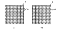
液晶表示パネル2は、バックライトユニット(図示せず)と、互いに並行に配列された走査線(ソース線)41,…,41と、これら走査線41,…,41と離間して交差するように配列されたデータ線(ソース線)31A,31B,31A,31B,…,31A,31Bとを有する。図1において、符号31Aは奇数番目のデータ線を、符号31Bは偶数番目のデータ線をそれぞれ示している。データ線31A,31Bと走査線41との各交差点付近には表示画素DPが設けられている。図1に示されるように、これら表示画素DP,…,DPは2次元配列されており、各表示画素DPが、一対の画素電極及び対向電極に挟まれた液晶層を有する液晶表示素子(容量性負荷)22と、この液晶表示素子22への電界の印加を制御するTFTなどの能動素子21とを含む。画素電極には能動素子21の被制御端子の一方が接続され、対向電極には、電源回路6から供給されたコモン電圧が印加される。また、能動素子21の被制御端子の他方はデータ線31Aまたはデータ線31Bに接続され、能動素子21の制御端子(ゲート)は走査線41に接続されている。
The liquid
コントローラ5は、外部の信号源(図示せず)から供給されたデータ信号に画像処理を施してデジタルデータDDを生成し、これを水平表示ライン単位でソースドライバ3に出力する。ゲートドライバ4は、走査線41,…,41に順次パルス電圧を出力して能動素子21をオン状態にする。ソースドライバ3は、デジタルデータDDをアナログ階調電圧(以下、単に「階調電圧」と呼ぶ。)に変換し、これら階調電圧をインピーダンス変換してデータ線31A,31B,…,31A,31Bにパラレル出力することにより、オン状態の能動素子21を介して液晶表示素子22の画素電極に階調電圧を印加することができる。各表示画素DPはその階調電圧を保持する。この結果、液晶表示素子22の画素電極と対向電極との間には階調電圧とコモン電圧との電圧差に応じた電界が形成される。液晶表示素子22では、形成された電界に応じて液晶分子が配向し、液晶分子の配向状態に応じた光透過率が形成される。
The
図3は、実施の形態1のソースドライバ3の構成例を概略的に示す図である。図3に示されるように、ソースドライバ3は、シフトレジスタ32,2ラインラッチ回路33,ライン切替回路34,レベルシフト回路35,電圧変換回路36,インピーダンス変換回路37,ライン切替回路38及び階調電圧発生回路39を有する。
FIG. 3 is a diagram schematically illustrating a configuration example of the
インピーダンス変換回路37は、ボルテージフォロアタイプの低圧側オペアンプ37Aと、ボルテージフォロアタイプの高圧側オペアンプ37Bとの組を複数有している。図4は、これら低圧側オペアンプ37Aと高圧側オペアンプ37Bとを概略的に示す図である。図4に示されるように、高圧側オペアンプ37Bは、電源電圧VDDとこの電源電圧VDDよりも低い共通電源電圧VMMとを用いて動作する非反転増幅器であり、低圧側オペアンプ37Aは、共通電源電圧VMMとこの共通電源電圧VMMよりも低い電源電圧VSSとを用いて動作する非反転増幅器である。
The
図3のシフトレジスタ32は、コントローラ5から転送されたデジタルデータ(多値階調データ)DDを取り込み、データ線31A,31B,…,31A,31Bと一対一で対応する配線ラインSa,Sb,…,Sa,Sbを介して1水平表示ライン分のデジタルデータを2ラインラッチ回路33にパラレルに出力する。ここで、符号Saは奇数番目のデータ線31Aに対応する配線ラインを、符号Sbは偶数番目のデータ線31Bに対応する配線ラインをそれぞれ示している。2ラインラッチ回路33は、シフトレジスタ32のパラレル出力をラッチするとともに、配線ラインSa,Sb,…,Sa,Sbと一対一で対応する配線ラインRa,Rb,…,Ra,Rbを介して保持データをライン切替回路34にパラレルに出力する。
The
ライン切替回路34は、一対の配線ラインRa,Rb毎に設けられたスイッチ回路341を有する。各スイッチ回路341は、コントローラ5からの制御信号SW1に応じて動作する。ライン切替回路34よりも後段にあるレベルシフト回路35は、負極性の階調電圧用のレベルシフタ35Aと正極性の階調電圧用のレベルシフタ35Bとの組を有している。スイッチ回路341は、あるタイミングで、一対の配線ラインRa,Rbのうち一方の配線ラインRaをレベルシフタ35Aに接続すると同時に、他方の配線ラインRbをレベルシフタ35Bに接続することにより、配線ラインRaから伝達した信号をレベルシフタ35Aに供給し、且つ、配線ラインRbから伝達した信号をレベルシフタ35Bに供給する。以下、このときのスイッチ回路341の接続形態を「ストレート接続」と呼ぶこととする。一方、別のタイミングでは、スイッチ回路341は、一方の配線ラインRaをレベルシフタ35Bに接続すると同時に、他方の配線ラインRbをレベルシフタ35Aに接続することにより、配線ラインRaから伝達した信号をレベルシフタ35Bに供給し、且つ、配線ラインRbから伝達した信号をレベルシフタ35Aに供給する。以下、このときのスイッチ回路341の接続形態を「クロス接続」と呼ぶこととする。
The
階調電圧発生回路39は、電源回路6から供給された電圧から、基準電圧(たとえば、GNDレベル)よりも高い2N個のレベル(Nは正整数)の正極性の階調電圧群VPと、基準電圧よりも低い2N個のレベルの負極性の階調電圧群VNとを生成し、これらを電圧変換回路36に供給する。たとえば、8ビット階調の表示を行う場合、28(=256)個のレベルの正極性の階調電圧と、28レベルの負極性の階調電圧とが生成される。電圧変換回路36においては、階調電圧選択部36Aは、負極性の階調電圧群VNの中から、レベルシフタ35Aの出力に対応する階調電圧を選択しこれを低圧側オペアンプ37Aに入力させる。また、階調電圧選択部36Bは、正極性の階調電圧群VPの中から、レベルシフタ35Bの出力に対応する階調電圧を選択しこれを高圧側オペアンプ37Bに入力させる。
The gradation
ライン切替回路38は、低圧側オペアンプ37Aと高圧側オペアンプ37Bの組ごとに設けられたスイッチ回路381を有する。各スイッチ回路381は、コントローラ5から供給された制御信号SW2に応じて動作する。上記スイッチ回路341がストレート接続しているとき、スイッチ回路381は、低圧側オペアンプ37Aの出力端子をデータ線31Aの一端に接続すると同時に、高圧側オペアンプ37Bの出力端子をデータ線31Bの一端に接続する。このときのスイッチ回路381の接続形態も「ストレート接続」と呼ぶこととする。このとき、奇数番目のデータ線31Aには負極性の階調電圧が印加され、偶数番目のデータ線31Bには正極性の階調電圧が印加される。一方、上記スイッチ回路341がクロス接続しているとき、スイッチ回路381は、低圧側オペアンプ37Aの出力端子をデータ線31Bの一端に接続すると同時に、高圧側オペアンプ37Bの出力端子をデータ線31Aの一端に接続する。このときのスイッチ回路381の接続形態も「クロス接続」と呼ぶこととする。このとき、奇数番目のデータ線31Aには正極性の階調電圧が印加され、偶数番目のデータ線31Bには負極性の階調電圧が印加される。
The
ライン切替回路34におけるスイッチ回路341の接続形態とライン切替回路38におけるスイッチ回路381の接続形態との組み合わせにより、反転駆動方式で液晶表示パネル2を駆動することが可能となる。図5(A),(B)は、ドット反転方式の駆動法を説明するための図であり、図6(A),(B)は、ライン反転方式の駆動法を説明するための図である。図5(A),(B)及び図6(A),(B)中、「+」の記号は、表示画素DPが正極性の階調電圧を保持すること意味し、「−」の記号は、表示画素DPが負極性の階調電圧を保持することを意味する。
By combining the connection form of the
図5(A),(B)では、水平表示方向に隣り合う表示画素DP,DPはいずれも互いに逆極性の階調電圧を保持し、垂直表示方向に隣り合う表示画素DP,DPも互いに逆極性の階調電圧を保持する。図5(A)の状態と図5(B)の状態とは、たとえば、フレーム単位またはフィールド単位で交互に切り替えられる。一方、図6(A),(B)では、垂直表示方向に隣り合う表示画素DP,DPは互いに同一極性の階調電圧を保持するが、水平表示方向に隣り合う表示ラインはいずれも互いに逆極性の階調電圧を保持する。図6(A)の状態と図6(B)の状態とは、たとえば、フレーム単位またはフィールド単位で交互に切り替えられる。 5A and 5B, the display pixels DP and DP adjacent to each other in the horizontal display direction hold gradation voltages having opposite polarities, and the display pixels DP and DP adjacent to each other in the vertical display direction are also opposite to each other. Holds the polarity gradation voltage. The state shown in FIG. 5A and the state shown in FIG. 5B are alternately switched in units of frames or fields, for example. On the other hand, in FIGS. 6A and 6B, the display pixels DP and DP adjacent in the vertical display direction hold the same polarity of gradation voltage, but the display lines adjacent in the horizontal display direction are opposite to each other. Holds the polarity gradation voltage. The state in FIG. 6A and the state in FIG. 6B are alternately switched in units of frames or fields, for example.
図7は、実施の形態1のソースドライバ3における低圧側オペアンプ37A及び高圧側オペアンプ37Bの概略構成と、これら低圧側オペアンプ37A及び高圧側オペアンプ37Bに対応するスイッチ回路381の概略構成とを示す図である。図7に示されるように、高圧側オペアンプ37Bは、差動増幅段50B、出力増幅段51B及び保護スイッチ回路62を含む。高圧側オペアンプ37Bの出力端子(ノード)NBは、差動増幅段50Bの反転入力端子(−)に接続されている。
FIG. 7 is a diagram showing a schematic configuration of the low-voltage side
出力増幅段51Bは、PMOSトランジスタ(pチャネル型電界効果トランジスタ)60Pと、NMOSトランジスタ(nチャネル型電界効果トランジスタ)61Nとを有する。NMOSトランジスタ61Nにおいては、ゲートは、差動増幅段50Bの出力端子と接続され、ソースは、共通電源電圧VMMを供給する電源ライン(以下、VMM電源ラインと呼ぶ。)と接続され、ドレインは、出力端子NBと接続されている。図7に示されるように、このNMOSトランジスタ61Nのバックゲートとドレインとの間にはpn接合ダイオード(寄生ダイオード)70が形成されている。一方、PMOSトランジスタ60Pにおいては、ソースは、電源電圧VDDを供給する電源ライン(以下、VDD電源ラインと呼ぶ。)と接続され、ドレインは、NMOSトランジスタ61Nのドレインと接続され、ゲートには定電圧が印加されている。また、PMOSトランジスタ60PのバックゲートはVDD電源ラインと接続されている。このPMOSトランジスタ60Pは定電流源として動作する。差動増幅段50Bの構成は、公知の構成であればよく、特に限定されるものではない。
The
保護スイッチ回路62は、MOSスイッチ621,622を含む。一方のMOSスイッチ621は、ゲート電圧(制御電圧)Vp1のレベルに応じて導通状態(オン状態)または非導通状態(オフ状態)となるPMOSトランジスタP1と、ゲート電圧(制御電圧)Vn1のレベルに応じて導通状態(オン状態)または非導通状態(オフ状態)となるNMOSトランジスタN1との対からなる。このMOSスイッチ621の一方の被制御端子はNMOSトランジスタ61Nのバックゲート(すなわち、寄生ダイオード70のアノード)と接続され、MOSスイッチ621の他方の被制御端子はVMM電源ラインと接続されている。他方のMOSスイッチ622は、ゲート電圧(制御電圧)Vp2のレベルに応じて導通状態(オン状態)または非導通状態(オフ状態)となるPMOSトランジスタP2と、ゲート電圧(制御電圧)Vn2のレベルに応じて導通状態(オン状態)または非導通状態(オフ状態)となるNMOSトランジスタN2の対からなる。このMOSスイッチ622の一方の被制御端子はNMOSトランジスタ61Nのバックゲート(すなわち、寄生ダイオード70のアノード)と接続され、MOSスイッチ622の他方の被制御端子は、電源電圧VSSを供給する電源ライン(以下、VSS電源ラインと呼ぶ。)と接続されている。図2のコントローラ5は、ゲート電圧Vn1,Vp1,Vn2,Vp2を切替制御信号として保護スイッチ回路62に供給する。
The
一方、低圧側オペアンプ37Aは、図7に示されるように、差動増幅段50A、出力増幅段51A及び保護スイッチ回路67を含む。低圧側オペアンプ37Aの出力端子(ノード)NAは、差動増幅段50Aの反転入力端子(−)に接続されている。
On the other hand, the low-voltage
出力増幅段51Aは、PMOSトランジスタ(pチャネル型電界効果トランジスタ)65Pと、NMOSトランジスタ(nチャネル型電界効果トランジスタ)66Nとを有する。PMOSトランジスタ65Pにおいては、ゲートは、差動増幅段50Aの出力端子と接続され、ソースは、VMM電源ラインと接続され、ドレインは、出力端子NAと接続されている。図7に示されるように、このPMOSトランジスタ65Pのバックゲートとドレインとの間にはpn接合ダイオードである寄生ダイオード71が形成されている。一方、NMOSトランジスタ66Nにおいては、ソースはVSS電源ラインと接続され、ドレインはPMOSトランジスタ65Pのドレインと接続され、ゲートには定電圧が印加されている。また、NMOSトランジスタ66NのバックゲートはVSS電源ラインと接続されている。このPMOSトランジスタ60Pは定電流源として動作する。差動増幅段50Aの構成は、公知の構成であればよく、特に限定されるものではない。
The
保護スイッチ回路67は、MOSスイッチ671,672を含む。一方のMOSスイッチ671は、ゲート電圧(制御電圧)Vp3のレベルに応じて導通状態(オン状態)または非導通状態(オフ状態)となるPMOSトランジスタP3と、ゲート電圧(制御電圧)Vn3のレベルに応じて導通状態(オン状態)または非導通状態(オフ状態)となるNMOSトランジスタN3との対からなる。このMOSスイッチ671の一方の被制御端子はPMOSトランジスタ65Pのバックゲート(すなわち、寄生ダイオード71のカソード)と接続され、MOSスイッチ671の他方の被制御端子はVMM電源ラインと接続されている。他方のMOSスイッチ672は、ゲート電圧(制御電圧)Vp4のレベルに応じて導通状態(オン状態)または非導通状態(オフ状態)となるPMOSトランジスタP4と、ゲート電圧(制御電圧)Vn4のレベルに応じて導通状態(オン状態)または非導通状態(オフ状態)となるNMOSトランジスタN4の対からなる。このMOSスイッチ672の一方の被制御端子はPMOSトランジスタ65Pのバックゲート(すなわち、寄生ダイオード71のカソード)と接続され、MOSスイッチ672の他方の被制御端子はVDD電源ラインと接続されている。図2のコントローラ5は、ゲート電圧Vn3,Vp3,Vn4,Vp4を切替制御信号として保護スイッチ回路67に供給する。
図7に示されるスイッチ回路381は、第1〜第4のMOSスイッチ382,383,384,385を含む。第1のMOSスイッチ382は、ゲート電圧(制御電圧)Vsp1のレベルに応じて導通状態(オン状態)または非導通状態(オフ状態)となるPMOSトランジスタSP1と、ゲート電圧(制御電圧)Vsn1のレベルに応じて導通状態(オン状態)または非導通状態(オフ状態)となるNMOSトランジスタSN1との対からなる。第2のMOSスイッチ383は、ゲート電圧(制御電圧)Vsp2のレベルに応じて導通状態(オン状態)または非導通状態(オフ状態)となるPMOSトランジスタSP2と、ゲート電圧(制御電圧)Vsn2のレベルに応じて導通状態(オン状態)または非導通状態(オフ状態)となるNMOSトランジスタSN2との対からなる。第3のMOSスイッチ384は、ゲート電圧(制御電圧)Vsp3のレベルに応じて導通状態(オン状態)または非導通状態(オフ状態)となるPMOSトランジスタSP3と、ゲート電圧(制御電圧)Vsn3のレベルに応じて導通状態(オン状態)または非導通状態(オフ状態)となるNMOSトランジスタSN3との対からなる。そして、第4のMOSスイッチ385は、ゲート電圧(制御電圧)Vsp4のレベルに応じて導通状態(オン状態)または非導通状態(オフ状態)となるPMOSトランジスタSP4と、ゲート電圧(制御電圧)Vsn4のレベルに応じて導通状態(オン状態)または非導通状態(オフ状態)となるNMOSトランジスタSN4との対からなる。
The
図2のコントローラ5は、ゲート電圧Vsp1,Vsn1,Vsp2,Vsn2,Vsp3,Vsn3,Vsp4,Vsn4をスイッチ回路381に供給してスイッチ回路381の接続形態を制御する。スイッチ回路381の接続形態がストレート接続のとき、MOSスイッチ382,385は、導通状態となり、出力端子NBをデータ線31Bに接続し、出力端子NAをデータ線31Aに接続する。また、MOSスイッチ383,384は非導通状態となる。他方、スイッチ回路381の接続形態がクロス接続のときは、MOSスイッチ383,384は、導通状態となり、出力端子NAをデータ線31Bに接続し、出力端子NBをデータ線31Aに接続する。また、MOSスイッチ382,385は非導通状態となる。
The
図8は、スイッチ回路381の接続形態がストレート接続とクロス接続との一方から他方へ切り替えられる際の制御信号波形を示すタイミングチャートである。図8には、スイッチ回路381に与えられるゲート電圧Vsp1,Vsn1,Vsp2,Vsn2,Vsp3,Vsn3,Vsp4,Vsn4の波形と、保護スイッチ回路62,67に供給されるゲート電圧Vp1,Vn1,Vp2,Vn2,Vp3,Vn3,Vp4,Vn4の波形と、出力端子NA,NBの電位Va,Vbとが示されている。
FIG. 8 is a timing chart showing control signal waveforms when the connection form of the
スイッチ回路381の接続形態がストレート接続からクロス接続に切り替えられるとき(時刻t1付近)、図8に示されるように、MOSスイッチ382,385を導通状態から非導通状態にするゲート電圧Vsp1,Vsn1,Vsp4,Vsn4が供給される。すなわち、PMOSトランジスタSP1,SP4のゲート電圧Vsp1,Vsp4の波形が立ち上げられ、NMOSトランジスタSN1,SN4のゲート電圧Vsn1,Vsn4の波形が立ち下げられる。同時に、MOSスイッチ383,384を非導通状態から導通状態にするゲート電圧Vsp2,Vsn2,Vsp3,Vsn3が供給される。すなわち、PMOSトランジスタSP2,SP3のゲート電圧Vsp2,Vsp3の波形が立ち下げられ、NMOSトランジスタSN2,SN3のゲート電圧Vsn2,Vsn3の波形が立ち上げられる。
When the connection form of the
高圧側オペアンプ37Bの保護スイッチ回路62では、スイッチ回路381の接続形態がストレート接続からクロス接続に切り替えられる直前(時刻t1の直前)に、MOSスイッチ621を導通状態から非導通状態にするゲート電圧Vn1,Vp1が供給される。すなわち、NMOSトランジスタN1のゲート電圧Vn1の波形が立ち下げられ、PMOSトランジスタP1のゲート電圧Vp1の波形が立ち上げられる。同時に、MOSスイッチ622を非導通状態から導通状態にするゲート電圧Vn2,Vp2が供給される。すなわち、図8に示されるように、NMOSトランジスタN2のゲート電圧Vn2の波形が立ち上げられ、PMOSトランジスタP2のゲート電圧Vp2の波形が立ち下げられる。
The
時刻t1から所定時間経過後は、MOSスイッチ621を非導通状態から導通状態にするゲート電圧Vn1,Vp1が供給される。すなわち、NMOSトランジスタN1のゲート電圧Vn1の波形が立ち上げられ、PMOSトランジスタP1のゲート電圧Vp1の波形が立ち下げられる。同時に、MOSスイッチ622を導通状態から非導通状態にするゲート電圧Vn2,Vp2が供給される。すなわち、NMOSトランジスタN2のゲート電圧Vn2の波形が立ち下げられ、PMOSトランジスタP2のゲート電圧Vp2の波形が立ち上げられる。
After a predetermined time has elapsed from the time t 1, the gate voltage Vn1, Vp1 to conductive
上記のとおり、時刻t1から所定時間の間、MOSスイッチ622が導通状態になることで、寄生ダイオード70のアノードに電源電圧VMMよりも低い電源電圧VSSが印加される。これにより、寄生ダイオード70に順方向バイアスが印加されることを確実に防止することができる。より具体的には、時刻t1の前には、高圧側オペアンプ37BはMOSスイッチ382を介してデータ線31Bに正極性の階調電圧を出力していたので、時刻t1の時点でデータ線31Bの電位は高い状態にある。また、低圧側オペアンプ37Aは、時刻t1の前には負極性の階調電圧をMOSスイッチ385を介してデータ線31Aに出力していたので、時刻t1の時点でデータ線31Aの電位は低い状態にある。時刻t1の経過後にスイッチ回路381の接続形態がクロス接続に切り替えられると、高圧側オペアンプ37Bの出力端子NBは、MOSスイッチ384を介して低電位のデータ線31Aに接続されるので、図8に示されるように出力端子NBの電位Vbは一時的に急峻に下降する。このとき、寄生ダイオード70のカソードの電位も下降するが、カソードの電位が下降する前に、寄生ダイオード70のアノードは、MOSスイッチ621(PMOSトランジスタP1及びNMOSトランジスタN1)によりVMM電源ラインから電気的に切り離され、且つ、MOSスイッチ622(PMOSトランジスタP2及びNMOSトランジスタN2)により電源電圧VSSに接続される。したがって、寄生ダイオード70への順方向バイアスの印加が確実に防止される。
As described above, between time t 1 for a predetermined time by
一方、低圧側オペアンプ37Aの保護スイッチ回路67では、スイッチ回路381の接続形態がストレート接続からクロス接続に切り替えられる直前(時刻t1の直前)に、MOSスイッチ671を導通状態から非導通状態にするゲート電圧Vn3,Vp3が供給される。すなわち、NMOSトランジスタN3のゲート電圧Vn3の波形が立ち下げられ、PMOSトランジスタP3のゲート電圧Vp3の波形が立ち上げられる。同時に、MOSスイッチ672を非導通状態から導通状態にするゲート電圧Vn4,Vp4が供給される。すなわち、図8に示されるように、NMOSトランジスタN4のゲート電圧Vn4の波形が立ち上げられ、PMOSトランジスタP4のゲート電圧Vp4の波形が立ち下げられる。
On the other hand, the
時刻t1から所定時間経過後は、MOSスイッチ671を非導通状態から導通状態にするゲート電圧Vn3,Vp3が供給される。すなわち、NMOSトランジスタN3のゲート電圧Vn3の波形が立ち上げられ、PMOSトランジスタP3のゲート電圧Vp3の波形が立ち下げられる。同時に、MOSスイッチ672を導通状態から非導通状態にするゲート電圧Vn4,Vp4が供給される。すなわち、NMOSトランジスタN4のゲート電圧Vn4の波形が立ち下げられ、PMOSトランジスタP4のゲート電圧Vp4の波形が立ち上げられる。
After a predetermined time has elapsed from the time t 1, the gate voltage Vn3, Vp3 to conductive
上記のとおり、時刻t1から所定時間の間、MOSスイッチ672が導通状態になることで、寄生ダイオード71のカソードに電源電圧VMMよりも高い電源電圧VDDが印加される。これにより、寄生ダイオード71に順方向バイアスが印加されることを確実に防止することができる。より具体的には、時刻t1の経過後にスイッチ回路381の接続形態がクロス接続に切り替えられると、低圧側オペアンプ37Aの出力端子NAは、MOSスイッチ383を介して高電位のデータ線31Bに接続されるので、図8に示されるように出力端子NAの電位Vaは一時的に急峻に上昇する。このとき、寄生ダイオード71のアノードの電位も上昇するが、アノードの電位が上昇する前に、寄生ダイオード71のカソードは、MOSスイッチ671(PMOSトランジスタP3及びNMOSトランジスタN3)によりVMM電源ラインから電気的に切り離され、且つ、MOSスイッチ672(PMOSトランジスタP4及びNMOSトランジスタN4)により電源電圧VDDに接続される。したがって、寄生ダイオード71への順方向バイアスの印加が確実に防止される。
As described above, between time t 1 for a predetermined time by
次に、スイッチ回路381の接続形態がクロス接続からストレート接続に切り替えられるとき(時刻t2付近)、図8に示されるように、MOSスイッチ383,384を導通状態から非導通状態にするゲート電圧Vsp2,Vsn2,Vsp3,Vsn3が供給される。すなわち、PMOSトランジスタSP2,SP3のゲート電圧Vsp2,Vsp3の波形が立ち上げられ、NMOSトランジスタSN2,SN3のゲート電圧Vsn2,Vsn3の波形が立ち下げられる。同時に、MOSスイッチ382,385を非導通状態から導通状態にするゲート電圧Vsp1,Vsn1,Vsp4,Vsn4が供給される。すなわち、PMOSトランジスタSP1,SP4のゲート電圧Vsp1,Vsp4の波形が立ち下げられ、NMOSトランジスタSN1,SN4のゲート電圧Vsn1,Vsn4の波形が立ち上げられる。
Next, when the connection form of the
高圧側オペアンプ37Bの保護スイッチ回路62では、スイッチ回路381の接続形態がクロス接続からストレート接続に切り替えられる直前(時刻t2の直前)に、MOSスイッチ621を導通状態から非導通状態にするゲート電圧Vn1,Vp1が供給される。同時に、MOSスイッチ622を非導通状態から導通状態にするゲート電圧Vn2,Vp2が供給される。
The
時刻t2から所定時間経過後は、MOSスイッチ621を非導通状態から導通状態にするゲート電圧Vn1,Vp1が供給される。同時に、MOSスイッチ622を導通状態から非導通状態にするゲート電圧Vn2,Vp2が供給される。
After the time t 2 a predetermined time has elapsed, the gate voltage Vn1, Vp1 to conductive
上記のとおり、時刻t2から所定時間の間、MOSスイッチ622が導通状態になることで、寄生ダイオード70のアノードに電源電圧VMMよりも低い電源電圧VSSが印加される。これにより、寄生ダイオード70に順方向バイアスが印加されることを確実に防止することができる。より具体的には、時刻t2の前には、高圧側オペアンプ37BはMOSスイッチ384を介してデータ線31Aに正極性の階調電圧を出力していたので、時刻t2の時点でデータ線31Aの電位は高い状態にある。また、低圧側オペアンプ37Aは、時刻t2の前には負極性の階調電圧をMOSスイッチ383を介してデータ線31Bに出力していたので、時刻t2の時点でデータ線31Bの電位は低い状態にある。時刻t2の経過後にスイッチ回路381の接続形態がストレート接続に切り替えられると、高圧側オペアンプ37Bの出力端子NBは、MOSスイッチ382を介して低電位のデータ線31Bに接続されるので、図8に示されるように出力端子NBの電位Vbは一時的に急峻に下降する。このとき、寄生ダイオード70のカソードの電位も下降するが、カソードの電位が下降する前に、寄生ダイオード70のアノードは、MOSスイッチ621(PMOSトランジスタP1及びNMOSトランジスタN1)によりVMM電源ラインから電気的に切り離され、且つ、MOSスイッチ622(PMOSトランジスタP2及びNMOSトランジスタN2)により電源電圧VSSに接続される。したがって、寄生ダイオード70への順方向バイアスの印加が確実に防止される。
As described above, the
一方、低圧側オペアンプ37Aの保護スイッチ回路67では、スイッチ回路381の接続形態がクロス接続からストレート接続に切り替えられる直前(時刻t2の直前)に、MOSスイッチ671を導通状態から非導通状態にするゲート電圧Vn3,Vp3が供給される。同時に、MOSスイッチ672を非導通状態から導通状態にするゲート電圧Vn4,Vp4が供給される。
On the other hand, the
時刻t2から所定時間経過後は、MOSスイッチ671を非導通状態から導通状態にするゲート電圧Vn3,Vp3が供給される。同時に、MOSスイッチ672を導通状態から非導通状態にするゲート電圧Vn4,Vp4が供給される。
After the time t 2 a predetermined time has elapsed, the gate voltage Vn3, Vp3 to conductive
上記のとおり、時刻t2から所定時間の間、MOSスイッチ672が導通状態になることで、寄生ダイオード71のカソードに電源電圧VMMよりも高い電源電圧VDDが印加される。これにより、寄生ダイオード71に順方向バイアスが印加されることを確実に防止することができる。より具体的には、時刻t2の経過後にスイッチ回路381の接続形態がストレート接続に切り替えられると、低圧側オペアンプ37Aの出力端子NAは、MOSスイッチ385を介して高電位のデータ線31Aに接続されるので、図8に示されるように出力端子NAの電位Vaは一時的に急峻に上昇する。このとき、寄生ダイオード71のアノードの電位も上昇するが、アノードの電位が上昇する前に、寄生ダイオード71のカソードは、MOSスイッチ671(PMOSトランジスタP3及びNMOSトランジスタN3)によりVMM電源ラインから電気的に切り離され、且つ、MOSスイッチ672(PMOSトランジスタP4及びNMOSトランジスタN4)により電源電圧VDDに接続される。したがって、寄生ダイオード71への順方向バイアスの印加が確実に防止される。
As described above, between time t 2 for a predetermined time, by
以上説明したように、高圧側オペアンプ37Bの出力端子NBの接続先がデータ線31B,31Aの一方から他方へ切り替えられることにより出力端子NBの電位が下降するときは、保護スイッチ回路62が寄生ダイオード70のアノードをVSS電源ラインと一時的に接続するので、寄生ダイオード70への順方向バイアスの印加を確実に防止することができる。また、低圧側オペアンプ37Aの出力端子NAの接続先がデータ線31B,31Aの一方から他方へ切り替えられることにより出力端子NAの電位が上昇するときは、保護スイッチ回路67が寄生ダイオード71のカソードをVDD電源ラインと一時的に接続するので、寄生ダイオード71への順方向バイアスの印加を確実に防止することができる。したがって、寄生ダイオード70,71に過電流が流れることが防止される。
As described above, when the connection destination of the output terminal NB of the high-voltage
図9は、保護スイッチ回路62,67を持たない高圧側オペアンプ37Bc及び低圧側オペアンプ37Acの比較例の構成を概略的に示す図である。図9の構成は、保護スイッチ回路62,67を持たない点を除いて、図7の構成とほぼ同じある。以下、図9を参照しつつ、寄生ダイオード70,71に過電流が流れた場合に低圧側オペアンプ37Ac及び高圧側オペアンプ37Bcの回路が破壊されるメカニズムについて説明する。
FIG. 9 is a diagram schematically showing a configuration of a comparative example of the high-voltage side operational amplifier 37Bc and the low-voltage side operational amplifier 37Ac that do not have the
上述のとおり、スイッチ回路381の接続形態が切り替えられるとき、高圧側オペアンプ37Bcの出力端子NBの電位Vbが急峻に下降する。このとき、出力端子NBの電位Vbが電源電圧VMMを下回り、寄生ダイオード70に大きな順方向バイアスが印加されると、NMOSトランジスタ61Nを構成するnpn型寄生バイポーラトランジスタ(寄生ダイオード70を含む。)がオン状態になり、寄生バイポーラトランジスタに過電流が流れる現象(バイポーラアクション)が生じる。この種の過電流は、高圧側オペアンプ37Bcの内部素子を破壊してしまう。また、上述のとおり、スイッチ回路381の接続形態が切り替えられるときには、低圧側オペアンプ37Acの出力端子NAの電位Vaが急峻に上昇する。このとき、出力端子NAの電位Vaが電源電圧VMMを上回り、寄生ダイオード71に大きな順方向バイアスが印加されると、PMOSトランジスタ65Pを構成するpnp型寄生バイポーラトランジスタ(寄生ダイオード71を含む。)がオン状態になり、この寄生バイポーラトランジスタにバイポーラアクションが生じる。この種の過電流は、低圧側オペアンプ37Acの内部素子を破壊してしまう。
As described above, when the connection form of the
これに対し、本実施の形態では、図7のスイッチ回路381の接続形態が切り替えられるとき、寄生ダイオード70,71に順方向バイアスが印加されないので、バイポーラアクションの発生を防止することができる。
On the other hand, in this embodiment, when the connection form of the
実施の形態2.
次に、本発明に係る実施の形態2について説明する。図10は、実施の形態2のソースドライバ3Mの構成例を概略的に示す図である。図11は、このソースドライバ3Mにおける低圧側オペアンプ37C及び高圧側オペアンプ37Dの概略構成と、これら低圧側オペアンプ37C及び高圧側オペアンプ37Dに対応するスイッチ回路381の構成とを示す図である。
Next, a second embodiment according to the present invention will be described. FIG. 10 is a diagram schematically illustrating a configuration example of the
本実施の形態のソースドライバ3M(図10)の構成は、インピーダンス変換回路37M及び電源電圧生成回路40を除いて、実施の形態1のソースドライバ3(図3)の構成と同じである。本実施の形態のインピーダンス変換回路37Mは、ボルテージフォロアタイプの低圧側オペアンプ37Cと、ボルテージフォロアタイプの高圧側オペアンプ37Dとの組を複数有している。
The configuration of the
電源電圧生成回路40は、電源電圧VDD,VSS,VMMのいずれかに基づいて電源電圧VPP,VLLを生成する回路である。電源電圧VPP(=VMM+α)は、電源電圧VDDよりも低く且つ共通電源電圧VMMよりも電圧αだけ高い。一方、電源電圧VLL(=VMM−β)は、電源電圧VSSよりも高く且つ共通電源電圧VMMよりも電圧βだけ低い。電圧α,βは、それぞれ、高圧側オペアンプ37D,37Cの特性に合わせて適宜設定すればよい。
The power supply
図11に示されるように、低圧側オペアンプ37Cは、差動増幅段50A、出力増幅段51A及び保護スイッチ回路67を有する。この低圧側オペアンプ37Cの構成は、MOSスイッチ672の一方の被制御端子が電源電圧VPPの供給ラインに接続されている点を除いて、実施の形態1の低圧側オペアンプ37Aの構成と同じである。一方、高圧側オペアンプ37Dは、差動増幅段50B、出力増幅段51B及び保護スイッチ回路62を有する。この高圧側オペアンプ37Dの構成は、MOSスイッチ622の一方の被制御端子が電源電圧VLLの供給ラインに接続されている点を除いて、実施の形態1の高圧側オペアンプ37Bの構成と同じである。
As shown in FIG. 11, the low-voltage side
本実施の形態では、実施の形態1の高圧側オペアンプ37B及び低圧側オペアンプ37Aに代えて、高圧側オペアンプ37D及び低圧側オペアンプ37Cが使用される。また、スイッチ回路381の接続形態がストレート接続とクロス接続との一方から他方へ切り替えられる際には、図8に示した制御信号が供給される。
In the present embodiment, a high-voltage
本実施の形態でも、高圧側オペアンプ37Dの出力端子NBの接続先がデータ線31B,31Aの一方から他方へ切り替えられることにより低圧側オペアンプ37Dの出力端子NBの電位が一時的に下降する。このとき、高圧側の保護スイッチ回路62のMOSスイッチ622は、寄生ダイオード70のアノードに対して共通電源電圧VMMよりも低く且つ電源電圧VSSよりも高い電源電圧VLLを所定時間に亘って印加するので、寄生ダイオード70への順方向バイアスの印加を抑制することができる。また、電源電圧VSSよりも高い電源電圧VLLが寄生ダイオード70のアノードに印加されるので、実施の形態1の場合と比べると、NMOSトランジスタ61Nのバックゲートの充放電時間を短くすることができる。
Also in the present embodiment, the potential of the output terminal NB of the low-voltage
また、低圧側オペアンプ37Cの出力端子NAの接続先がデータ線31B,31Aの一方から他方へ切り替えられることにより低圧側オペアンプ37Cの出力端子NAの電位が一時的に上昇する。このとき、低圧側の保護スイッチ回路67のMOSスイッチ672は、寄生ダイオード71のカソードに対して共通電源電圧VMMよりも高く且つ電源電圧VDDよりも低い電源電圧VPPを所定時間に亘って印加するので、寄生ダイオード71への順方向バイアスの印加を抑制することができる。また、電源電圧VDDよりも低い電源電圧VPPが寄生ダイオード71のカソードに印加されるので、実施の形態1の場合と比べると、PMOSトランジスタ65Pのバックゲートの充放電時間を短くすることができる。
Further, the connection destination of the output terminal NA of the low-voltage
上記したように、スイッチ回路381の接続形態が切り替えられる際、高圧側オペアンプ37D及び低圧側オペアンプ37Cを構成するNMOSトランジスタ61N及びPMOSトランジスタ65Pのバックゲートの充放電時間を短くすることができる。このため、実施の形態1の場合と比べると、出力増幅段51B,51Aの電流駆動能力を短時間で元に戻すことができる。また、高圧側オペアンプ37D及び低圧側オペアンプ37Cの消費電力の低減も可能となる。
As described above, when the connection form of the
実施の形態1,2の変形例.
以上、図面を参照して本発明に係る種々の実施の形態について述べたが、これらは本発明の例示であり、上記以外の様々な形態を採用することもできる。たとえば、表示画素DPは、液晶表示素子以外の容量性負荷を有するものでもよい。
Modifications of the first and second embodiments.
Although various embodiments according to the present invention have been described above with reference to the drawings, these are examples of the present invention, and various forms other than the above can be adopted. For example, the display pixel DP may have a capacitive load other than the liquid crystal display element.
また、上記実施の形態1,2の低圧側オペアンプ37A,37Cと高圧側オペアンプ37B,37Dの構成は、特に限定されるものではなく、共通電源電圧VMMの電源ラインと出力端子NBとの間、もしくは、共通電源電圧VMMの電源ラインと出力端子NAとの間に、寄生ダイオードを含む寄生バイポーラトランジスタが形成される構成であればよい。
Further, the configurations of the low-voltage side
また、上記低圧側オペアンプ37A,37Cと高圧側オペアンプ37B,37Dとは、共通電源電圧VMMを使用しているが、これに限定されるものではない。高圧側オペアンプ37B,37Dが、電源電圧VMM1と電源電圧VDD(VMM1<VDD)とを用いて動作し、低圧側オペアンプ37A,37Cが、電源電圧VSSと電源電圧VMM2(VMM1>VMM2>VSS;VMM1≠VMM2)とを用いて動作する形態もあり得る。図12は、このような形態の高圧側オペアンプ37Bm及び低圧側オペアンプ37Amの一例を示す図である。
The low-voltage side
また、低圧側オペアンプ37A,37Cと高圧側オペアンプ37B,37Dは、入力電圧と出力電圧の両方の範囲が電源電圧の範囲まで動作可能なレール・ツー・レール(Rail−to−Rail)型オペアンプでもよい。また、差動増幅段50A,50Bの構成も限定されるものではなく、吸い込み(シンク)型または吐き出し(ソース)型のいずれの回路を含むものであってよい。
The low-voltage side
1 液晶表示装置、 2 液晶表示パネル、 3,3M ソースドライバ、 4 ゲートドライバ、 5 コントローラ、 6 電源回路、 21 アクティブ素子(能動素子)、 22 液晶表示素子、 31A,31B データ線(ソース線)、 32 シフトレジスタ、 33 2ラインラッチ回路、 34 ライン切替回路、 341 スイッチ回路、 35 レベルシフト回路、 35A,35B レベルシフタ、 36 電圧変換回路、 36A,36B 階調電圧選択部、 37,37M インピーダンス変換回路、 37A,37C 低圧側オペアンプ、 37B,37D 高圧側オペアンプ、 38 ライン切替回路、 381 スイッチ回路、 382〜385 MOSスイッチ、 39 階調電圧発生回路、 40 電源電圧生成回路、 41 走査線(ゲート線)、 62,67 保護スイッチ回路、 621,622,671,672 MOSスイッチ、 70 寄生ダイオード、 71 寄生ダイオード。
DESCRIPTION OF
Claims (15)
第1電源電圧と該第1電源電圧よりも低い第2電源電圧とを用いて動作して正極性の直流電圧成分を有するアナログ電圧を出力する第1のオペアンプと、
第3電源電圧と該第3電源電圧よりも低い第4電源電圧とを用いて動作して負極性の直流電圧成分を有するアナログ電圧を出力する第2のオペアンプと、
前記第1のオペアンプの出力端子の接続先を前記複数のデータ線のうちの第1のデータ線から該第1のデータ線とは異なる第2のデータ線へ切り替えると同時に、前記第2のオペアンプの出力端子の接続先を前記第2のデータ線から前記第1のデータ線に切り替えるスイッチ回路と、
を備え、
前記第1のオペアンプは、
前記第1のオペアンプにおいて形成された、前記第2電源電圧を供給する電源ラインに接続されたアノードと前記第1のオペアンプの出力端子に接続されたカソードとを有する第1の寄生ダイオードと、
第1の保護スイッチ回路と
を含み、
前記スイッチ回路が前記第1のオペアンプの出力端子の接続先を前記第1のデータ線から前記第2のデータ線に切り替える場合に、
前記第1の保護スイッチ回路は、
前記スイッチ回路により前記第1のオペアンプの出力端子の接続先が前記第1のデータ線から電気的に切り離される直前に、前記第1の寄生ダイオードのアノードを前記第2電源電圧を供給する前記電源ラインから電気的に切り離し且つ前記第1の寄生ダイオードのアノードを前記第2電源電圧よりも低い電圧を供給する第1の電圧供給ラインに接続し、
前記スイッチ回路により前記第1のオペアンプの出力端子の接続先が前記第2のデータ線に接続された後に、前記第1の寄生ダイオードのアノードを、前記第1の電圧供給ラインから電気的に切り離し且つ前記第2電源電圧を供給する前記電源ラインに接続する
ことを特徴とする駆動回路。 A plurality of signal lines, a plurality of data lines arranged so as to intersect with the plurality of signal lines, and a capacitive load formed in a region near an intersection of the signal lines and the data lines, respectively. A drive circuit for driving a display panel having
A first operational amplifier that operates using a first power supply voltage and a second power supply voltage lower than the first power supply voltage and outputs an analog voltage having a positive DC voltage component;
A second operational amplifier that operates using a third power supply voltage and a fourth power supply voltage lower than the third power supply voltage and outputs an analog voltage having a negative DC voltage component;
At the same time as switching the connection destination of the output terminal of the first operational amplifier from the first data line of the plurality of data lines to a second data line different from the first data line, the second operational amplifier A switch circuit for switching the connection destination of the output terminal from the second data line to the first data line;
With
The first operational amplifier is:
A first parasitic diode formed in the first operational amplifier and having an anode connected to a power supply line for supplying the second power supply voltage and a cathode connected to an output terminal of the first operational amplifier;
A first protection switch circuit;
When the switch circuit switches the connection destination of the output terminal of the first operational amplifier from the first data line to the second data line,
The first protection switch circuit includes:
The power supply that supplies the second power supply voltage to the anode of the first parasitic diode immediately before the connection destination of the output terminal of the first operational amplifier is electrically disconnected from the first data line by the switch circuit. Electrically disconnecting from the line and connecting the anode of the first parasitic diode to a first voltage supply line supplying a voltage lower than the second power supply voltage;
After the connection destination of the output terminal of the first operational amplifier is connected to the second data line by the switch circuit, the anode of the first parasitic diode is electrically disconnected from the first voltage supply line. And a drive circuit connected to the power supply line for supplying the second power supply voltage.
前記第1の保護スイッチ回路は、
前記第1のオペアンプから出力された当該アナログ電圧が前記スイッチ回路を介して前記第1のデータ線に供給される間は、前記nチャネル型電界効果トランジスタのバックゲートを前記第2電源電圧を供給する電源ラインに接続し、
前記スイッチ回路により前記第1のオペアンプの出力端子の接続先が前記第1のデータ線から前記第2のデータ線へ切り替えられるときは、前記nチャネル型電界効果トランジスタのバックゲートを前記第2電源電圧を供給する電源ラインから電気的に切り離す、
ことを特徴とする駆動回路。 The drive circuit according to claim 2,
The first protection switch circuit includes:
While the analog voltage output from the first operational amplifier is supplied to the first data line via the switch circuit, the second power supply voltage is supplied to the back gate of the n-channel field effect transistor. Connected to the power line
When the connection destination of the output terminal of the first operational amplifier is switched from the first data line to the second data line by the switch circuit, the back gate of the n-channel field effect transistor is connected to the second power source. Electrically disconnect from the power line that supplies the voltage,
A drive circuit characterized by that.
前記第2のオペアンプは、
前記第2のオペアンプにおいて形成された、前記第3電源電圧を供給する電源ラインに接続されたカソードと前記第2のオペアンプの出力端子に接続されたアノードとを有する第2の寄生ダイオードと、
前記スイッチ回路により前記第2のオペアンプの出力端子の接続先が前記第2のデータ線から電気的に切り離される直前に、前記第2の寄生ダイオードのカソードを前記第3電源電圧を供給する前記電源ラインから電気的に切り離し、且つ前記スイッチ回路により前記第2のオペアンプの出力端子の接続先が前記第1のデータ線に接続された後に、前記第2の寄生ダイオードのカソードを前記第3電源電圧よりも高い電圧を供給する第2の電圧供給ラインに接続する第2の保護スイッチ回路と、
を含むことを特徴とする駆動回路。 A drive circuit according to any one of claims 1 to 5,
The second operational amplifier is
A second parasitic diode formed in the second operational amplifier and having a cathode connected to a power supply line for supplying the third power supply voltage and an anode connected to an output terminal of the second operational amplifier;
The power supply that supplies the third power supply voltage to the cathode of the second parasitic diode immediately before the switch circuit electrically disconnects the output terminal of the second operational amplifier from the second data line. The second parasitic diode is connected to the first data line after being electrically disconnected from the line and connected to the output terminal of the second operational amplifier by the switch circuit. A second protection switch circuit connected to a second voltage supply line for supplying a higher voltage;
A drive circuit comprising:
第1電源電圧と該第1電源電圧よりも低い第2電源電圧とを用いて動作して正極性の直流電圧成分を有するアナログ電圧を出力する第1のオペアンプと、
第3電源電圧と該第3電源電圧よりも低い第4電源電圧とを用いて動作して負極性の直流電圧成分を有するアナログ電圧を出力する第2のオペアンプと、
前記第1のオペアンプの出力端子の接続先を前記複数のデータ線のうちの第1のデータ線から該第1のデータ線とは異なる第2のデータ線へ切り替えると同時に、前記第2のオペアンプの出力端子の接続先を前記第2のデータ線から前記第1のデータ線に切り替えるスイッチ回路と、
を備え、
前記第2のオペアンプは、
前記第2のオペアンプにおいて形成された、前記第3電源電圧を供給する電源ラインに接続されたカソードと前記第2のオペアンプの出力端子に接続されたアノードとを有する第2の寄生ダイオードと、
第2の保護スイッチ回路と
を含み
前記スイッチ回路が前記第2のオペアンプの出力端子の接続先を前記第2のデータ線から前記第1のデータ線に切り替える場合に、
前記第2の保護スイッチ回路は、
前記スイッチ回路により前記第2のオペアンプの出力端子の接続先が前記第2のデータ線から電気的に切り離される直前に、前記第2の寄生ダイオードのカソードを前記第3電源電圧を供給する前記電源ラインから電気的に切り離し且つ前記第2の寄生ダイオードのカソードを前記第3電源電圧よりも高い電圧を供給する第2の電圧供給ラインに接続し、
前記スイッチ回路により前記第2のオペアンプの出力端子の接続先が前記第1のデータ線に接続された後に、前記第2の寄生ダイオードのカソードを、前記第2の電圧供給ラインから電気的に切り離し且つ前記第3電源電圧を供給する前記電源ラインに接続する
ことを特徴とする駆動回路。 A plurality of signal lines, a plurality of data lines arranged so as to intersect with the plurality of signal lines, and a capacitive load formed in a region near an intersection of the signal lines and the data lines, respectively. A drive circuit for driving a display panel having
A first operational amplifier that operates using a first power supply voltage and a second power supply voltage lower than the first power supply voltage and outputs an analog voltage having a positive DC voltage component;
A second operational amplifier that operates using a third power supply voltage and a fourth power supply voltage lower than the third power supply voltage and outputs an analog voltage having a negative DC voltage component;
At the same time as switching the connection destination of the output terminal of the first operational amplifier from the first data line of the plurality of data lines to a second data line different from the first data line, the second operational amplifier A switch circuit for switching the connection destination of the output terminal from the second data line to the first data line;
With
The second operational amplifier is
A second parasitic diode formed in the second operational amplifier and having a cathode connected to a power supply line for supplying the third power supply voltage and an anode connected to an output terminal of the second operational amplifier;
When the switch circuit switches the connection destination of the output terminal of the second operational amplifier from the second data line to the first data line,
The second protection switch circuit includes:
The power supply that supplies the third power supply voltage to the cathode of the second parasitic diode immediately before the switch circuit electrically disconnects the output terminal of the second operational amplifier from the second data line. Electrically disconnecting from the line and connecting the cathode of the second parasitic diode to a second voltage supply line supplying a voltage higher than the third power supply voltage;
After the connection destination of the output terminal of the second operational amplifier is connected to the first data line by the switch circuit, the cathode of the second parasitic diode is electrically disconnected from the second voltage supply line. And a drive circuit connected to the power supply line for supplying the third power supply voltage.
前記第2の保護スイッチ回路は、
前記第2のオペアンプから出力された当該アナログ電圧が前記スイッチ回路を介して前記第2のデータ線に供給される間は、前記pチャネル型電界効果トランジスタのバックゲートを前記第3電源電圧を供給する電源ラインに接続し、
前記スイッチ回路により前記第2のオペアンプの出力端子の接続先が前記第2のデータ線から前記第1のデータ線に切り替えられたときは、前記pチャネル型電界効果トランジスタのバックゲートを前記第3電源電圧を供給する電源ラインから電気的に切り離す、
ことを特徴とする駆動回路。 The drive circuit according to claim 8, wherein
The second protection switch circuit includes:
While the analog voltage output from the second operational amplifier is supplied to the second data line via the switch circuit, the third power supply voltage is supplied to the back gate of the p-channel field effect transistor. Connected to the power line
When the connection destination of the output terminal of the second operational amplifier is switched from the second data line to the first data line by the switch circuit, the back gate of the p-channel field effect transistor is connected to the third gate. Electrically disconnected from the power supply line that supplies the power supply voltage,
A drive circuit characterized by that.
第1電源電圧と該第1電源電圧よりも低い第2電源電圧とを用いて動作して正極性の直流電圧成分を有するアナログ電圧を出力する第1のオペアンプと、
第3電源電圧と該第3電源電圧よりも低い第4電源電圧とを用いて動作して負極性の直流電圧成分を有するアナログ電圧を出力する第2のオペアンプと、
前記第1のオペアンプの出力端子の接続先を前記複数のデータ線のうちの第1のデータ線から該第1のデータ線とは異なる第2のデータ線へ切り替えると共に、前記第2のオペアンプの出力端子の接続先を前記第2のデータ線から前記第1のデータ線に切り替える動作を行う第1スイッチ回路と、
前記第2電源電圧を供給する電源ラインに接続された第1のアノードと前記第1のオペアンプの出力端子に接続された第1のカソードとを有する第1の寄生ダイオードと、
前記第3電源電圧を供給する電源ラインに接続された第2のカソードと前記第2のオペアンプの出力端子に接続された第2のアノードとを有する第2の寄生ダイオードと、
前記第1のアノードの接続先を、前記第2電源電圧を供給する前記電源ラインから前記第2電源電圧より低い電圧を供給する第1の電圧供給ラインに切り替えると共に、前記第2のカソードの接続先を、前記第3電源電圧を供給する前記電源ラインから前記第3電源電圧より高い電圧を供給する第2の電圧供給ラインに切り替える第2スイッチ回路と
を含み、
前記第2スイッチ回路は、
前記第1スイッチ回路の前記動作の直前において、
前記第1のアノードの接続先を、前記第2電源電圧を供給する前記電源ラインから前記第1の電圧供給ラインに切り替え、
前記第2のカソードの接続先を、前記第3電源電圧を供給する前記電源ラインから前記第2の電圧供給ラインに切り替え、
前記第1スイッチ回路により、前記第1のオペアンプの出力端子の接続先が前記第2のデータ線に接続され、前記第2のオペアンプの出力端子の接続先が前記第1のデータ線に接続された後に、
前記第1の寄生ダイオードの第1のアノードを、前記第1の電圧供給ラインから電気的に切り離し且つ前記第2電源電圧を供給する前記電源ラインに接続し、
前記第2の寄生ダイオードの第2のカソードを、前記第2の電圧供給ラインから電気的に切り離し且つ前記第3電源電圧を供給する前記電源ラインに接続する
ことを特徴とする駆動回路。 A plurality of signal lines, a plurality of data lines arranged so as to intersect with the plurality of signal lines, and a capacitive load formed in a region near an intersection of the signal lines and the data lines, respectively. A drive circuit for driving a display panel having
A first operational amplifier that operates using a first power supply voltage and a second power supply voltage lower than the first power supply voltage and outputs an analog voltage having a positive DC voltage component;
A second operational amplifier that operates using a third power supply voltage and a fourth power supply voltage lower than the third power supply voltage and outputs an analog voltage having a negative DC voltage component;
The connection destination of the output terminal of the first operational amplifier is switched from the first data line of the plurality of data lines to a second data line different from the first data line, and the second operational amplifier is connected to the second operational amplifier. A first switch circuit that performs an operation of switching the connection destination of the output terminal from the second data line to the first data line;
A first parasitic diode having a first anode connected to a power supply line for supplying the second power supply voltage and a first cathode connected to an output terminal of the first operational amplifier;
A second parasitic diode having a second cathode connected to a power supply line for supplying the third power supply voltage and a second anode connected to an output terminal of the second operational amplifier;
The connection destination of the first anode is switched from the power supply line that supplies the second power supply voltage to the first voltage supply line that supplies a voltage lower than the second power supply voltage , and the connection of the second cathode A second switch circuit for switching the tip from the power supply line for supplying the third power supply voltage to a second voltage supply line for supplying a voltage higher than the third power supply voltage ;
The second switch circuit includes:
Immediately before the operation of the first switch circuit,
Wherein the first anode connection destination, switches the second power supply voltage the to the power supply line or al before Symbol first voltage supply line for supplying,
Wherein the second cathode connection destination, switches the third power supply voltage the to the power supply line or al before Symbol second voltage supply line for supplying,
The first switch circuit connects the output terminal of the first operational amplifier to the second data line, and connects the output terminal of the second operational amplifier to the first data line. After
A first anode of the first parasitic diode is electrically disconnected from the first voltage supply line and connected to the power supply line supplying the second power supply voltage;
The drive characterized in that the second cathode of the second parasitic diode is electrically disconnected from the second voltage supply line and connected to the power supply line supplying the third power supply voltage. circuit.
Priority Applications (3)
| Application Number | Priority Date | Filing Date | Title |
|---|---|---|---|
| JP2010152957A JP5777300B2 (en) | 2010-07-05 | 2010-07-05 | Driving circuit and display device |
| US13/164,838 US8587507B2 (en) | 2010-07-05 | 2011-06-21 | Driving circuit and display apparatus having operational amplifiers with parasitic diodes |
| US14/052,952 US9202425B2 (en) | 2010-07-05 | 2013-10-14 | Device circuit and display apparatus having operational amplifiers with parasitic diodes |
Applications Claiming Priority (1)
| Application Number | Priority Date | Filing Date | Title |
|---|---|---|---|
| JP2010152957A JP5777300B2 (en) | 2010-07-05 | 2010-07-05 | Driving circuit and display device |
Publications (2)
| Publication Number | Publication Date |
|---|---|
| JP2012014105A JP2012014105A (en) | 2012-01-19 |
| JP5777300B2 true JP5777300B2 (en) | 2015-09-09 |
Family
ID=45399378
Family Applications (1)
| Application Number | Title | Priority Date | Filing Date |
|---|---|---|---|
| JP2010152957A Active JP5777300B2 (en) | 2010-07-05 | 2010-07-05 | Driving circuit and display device |
Country Status (2)
| Country | Link |
|---|---|
| US (2) | US8587507B2 (en) |
| JP (1) | JP5777300B2 (en) |
Families Citing this family (13)
| Publication number | Priority date | Publication date | Assignee | Title |
|---|---|---|---|---|
| US10420701B2 (en) * | 2013-05-17 | 2019-09-24 | Zoll Medical Corporation | Cameras for emergency rescue |
| TWI595471B (en) | 2013-03-26 | 2017-08-11 | 精工愛普生股份有限公司 | Amplification circuit, source driver, electrooptical device, and electronic device |
| CN103456277B (en) * | 2013-08-30 | 2017-02-22 | 合肥京东方光电科技有限公司 | Polarity-reversal driving method and polarity-reversal driving circuit |
| KR20160005560A (en) * | 2014-07-07 | 2016-01-15 | 주식회사 실리콘웍스 | Display driving circuit and output buffer circuit thereof |
| TWI560686B (en) * | 2014-11-28 | 2016-12-01 | Tenx Shenzhen Technology Ltd | Voltage follower and driving apparatus |
| CN104575355B (en) * | 2014-12-31 | 2017-02-01 | 深圳市华星光电技术有限公司 | Display panel and drive circuit thereof |
| US9576518B2 (en) | 2014-12-31 | 2017-02-21 | Shenzhen China Optoelectronics Technology Co., Ltd | Display panel and driving circuit thereof |
| US9607539B2 (en) | 2014-12-31 | 2017-03-28 | Shenzhen China Star Optoelectronics Technology Co., Ltd. | Display panel capable of reducing a voltage level changing frequency of a select signal and drive circuit thereof |
| CN104485063B (en) * | 2014-12-31 | 2016-08-17 | 深圳市华星光电技术有限公司 | Display floater and drive circuit thereof |
| US10102792B2 (en) * | 2016-03-30 | 2018-10-16 | Novatek Microelectronics Corp. | Driving circuit of display panel and display apparatus using the same |
| CN107146590B (en) * | 2017-07-06 | 2020-03-27 | 深圳市华星光电技术有限公司 | Driving method of GOA circuit |
| JP6966887B2 (en) * | 2017-07-26 | 2021-11-17 | ラピスセミコンダクタ株式会社 | Output circuit and display driver |
| US11114036B2 (en) * | 2018-06-08 | 2021-09-07 | Samsung Display Co., Ltd. | Scan driver and display device for driving a plurality of scan lines |
Family Cites Families (10)
| Publication number | Priority date | Publication date | Assignee | Title |
|---|---|---|---|---|
| JP3056085B2 (en) | 1996-08-20 | 2000-06-26 | 日本電気株式会社 | Drive circuit of matrix type liquid crystal display |
| JP4484729B2 (en) * | 2004-03-16 | 2010-06-16 | パナソニック株式会社 | DRIVE VOLTAGE GENERATOR AND CONTROL METHOD FOR DRIVE VOLTAGE GENERATOR |
| US7292217B2 (en) | 2004-03-18 | 2007-11-06 | Novatek Microelectronics Corp. | Source driver and liquid crystal display using the same |
| JP2006292807A (en) | 2005-04-06 | 2006-10-26 | Renesas Technology Corp | Semiconductor integrated circuit for liquid crystal display driving |
| JP2006337961A (en) * | 2005-06-06 | 2006-12-14 | Nec Electronics Corp | Driving circuit of liquid crystal panel, display apparatus, and method for driving liquid crystal panel |
| JP4840908B2 (en) * | 2005-12-07 | 2011-12-21 | ルネサスエレクトロニクス株式会社 | Display device drive circuit |
| JP5188023B2 (en) * | 2006-01-24 | 2013-04-24 | ラピスセミコンダクタ株式会社 | Driving device and driving method thereof |
| DE102007048454B3 (en) * | 2007-10-10 | 2009-03-19 | Texas Instruments Deutschland Gmbh | Electronic device, has current mirror transistors and power sources extracting currents from respective output nodes and designed such that one of currents about portion corresponding to leakage current is higher than other current |
| JP4954924B2 (en) * | 2008-03-11 | 2012-06-20 | ルネサスエレクトロニクス株式会社 | Differential amplifier and display device drive circuit using the same |
| WO2010114014A1 (en) * | 2009-04-01 | 2010-10-07 | ローム株式会社 | Liquid crystal driving apparatus |
-
2010
- 2010-07-05 JP JP2010152957A patent/JP5777300B2/en active Active
-
2011
- 2011-06-21 US US13/164,838 patent/US8587507B2/en active Active
-
2013
- 2013-10-14 US US14/052,952 patent/US9202425B2/en not_active Expired - Fee Related
Also Published As
| Publication number | Publication date |
|---|---|
| US20120001952A1 (en) | 2012-01-05 |
| US20140043221A1 (en) | 2014-02-13 |
| US9202425B2 (en) | 2015-12-01 |
| JP2012014105A (en) | 2012-01-19 |
| US8587507B2 (en) | 2013-11-19 |
Similar Documents
| Publication | Publication Date | Title |
|---|---|---|
| JP5777300B2 (en) | Driving circuit and display device | |
| US7786970B2 (en) | Driver circuit of display device | |
| US9147361B2 (en) | Output circuit, data driver and display device | |
| JP5374356B2 (en) | Driving circuit and display device | |
| US8390609B2 (en) | Differential amplifier and drive circuit of display device using the same | |
| US8368673B2 (en) | Output buffer and source driver using the same | |
| JP4840908B2 (en) | Display device drive circuit | |
| JP5780650B2 (en) | Level shifter circuit, scanning circuit, display device, and electronic device | |
| US6970152B1 (en) | Stacked amplifier arrangement for graphics displays | |
| JP2017098813A (en) | Level shift circuit and display driver | |
| JP2006337961A (en) | Driving circuit of liquid crystal panel, display apparatus, and method for driving liquid crystal panel | |
| US6392627B1 (en) | Liquid crystal display device and driver circuit thereof | |
| Son et al. | A column driver with low-power area-efficient push-pull buffer amplifiers for active-matrix LCDs | |
| CN100590744C (en) | Shifting register as well as drive circuit and display device using said shifting register | |
| JP2007312385A (en) | Level shifter | |
| US10607560B2 (en) | Semiconductor device and data driver | |
| JP6971078B2 (en) | Display driver and display device | |
| JP2010122510A (en) | Operational amplifier and driving device for display panel | |
| JP2009014971A (en) | Display driver circuit | |
| US7639227B2 (en) | Integrated circuit capable of synchronizing multiple outputs of buffers | |
| KR102641231B1 (en) | Scan driver | |
| JP5721444B2 (en) | Source driver and liquid crystal display device using the same | |
| JP2009017432A (en) | Level shift circuit, and display device | |
| JP5650297B2 (en) | Driving circuit and display device | |
| JP2011053623A (en) | Drive circuit of liquid crystal panel, and display device |
Legal Events
| Date | Code | Title | Description |
|---|---|---|---|
| A621 | Written request for application examination |
Free format text: JAPANESE INTERMEDIATE CODE: A621 Effective date: 20130621 |
|
| A977 | Report on retrieval |
Free format text: JAPANESE INTERMEDIATE CODE: A971007 Effective date: 20131129 |
|
| A131 | Notification of reasons for refusal |
Free format text: JAPANESE INTERMEDIATE CODE: A131 Effective date: 20131203 |
|
| A977 | Report on retrieval |
Free format text: JAPANESE INTERMEDIATE CODE: A971007 Effective date: 20131211 |
|
| A521 | Request for written amendment filed |
Free format text: JAPANESE INTERMEDIATE CODE: A523 Effective date: 20140131 |
|
| A131 | Notification of reasons for refusal |
Free format text: JAPANESE INTERMEDIATE CODE: A131 Effective date: 20140225 |
|
| A02 | Decision of refusal |
Free format text: JAPANESE INTERMEDIATE CODE: A02 Effective date: 20140701 |
|
| A521 | Request for written amendment filed |
Free format text: JAPANESE INTERMEDIATE CODE: A523 Effective date: 20140926 |
|
| A911 | Transfer to examiner for re-examination before appeal (zenchi) |
Free format text: JAPANESE INTERMEDIATE CODE: A911 Effective date: 20141006 |
|
| A521 | Request for written amendment filed |
Free format text: JAPANESE INTERMEDIATE CODE: A523 Effective date: 20150610 |
|
| A61 | First payment of annual fees (during grant procedure) |
Free format text: JAPANESE INTERMEDIATE CODE: A61 Effective date: 20150707 |
|
| R150 | Certificate of patent or registration of utility model |
Ref document number: 5777300 Country of ref document: JP Free format text: JAPANESE INTERMEDIATE CODE: R150 |