JP5735981B2 - Convert discrete-time quantized signals to continuous-time continuously variable signals - Google Patents
Convert discrete-time quantized signals to continuous-time continuously variable signals Download PDFInfo
- Publication number
- JP5735981B2 JP5735981B2 JP2012544832A JP2012544832A JP5735981B2 JP 5735981 B2 JP5735981 B2 JP 5735981B2 JP 2012544832 A JP2012544832 A JP 2012544832A JP 2012544832 A JP2012544832 A JP 2012544832A JP 5735981 B2 JP5735981 B2 JP 5735981B2
- Authority
- JP
- Japan
- Prior art keywords
- output
- input
- signal
- discrete
- noise shaping
- Prior art date
- Legal status (The legal status is an assumption and is not a legal conclusion. Google has not performed a legal analysis and makes no representation as to the accuracy of the status listed.)
- Active
Links
- 238000007493 shaping process Methods 0.000 claims description 120
- 238000013139 quantization Methods 0.000 claims description 111
- 230000004044 response Effects 0.000 claims description 81
- 238000012545 processing Methods 0.000 claims description 67
- 238000012546 transfer Methods 0.000 claims description 39
- 238000005070 sampling Methods 0.000 claims description 34
- 238000006243 chemical reaction Methods 0.000 claims description 26
- 230000009021 linear effect Effects 0.000 claims description 26
- 238000013507 mapping Methods 0.000 claims description 20
- 239000002131 composite material Substances 0.000 claims 4
- 238000005259 measurement Methods 0.000 claims 2
- 230000006870 function Effects 0.000 description 43
- 238000000034 method Methods 0.000 description 40
- 238000000354 decomposition reaction Methods 0.000 description 34
- 238000010586 diagram Methods 0.000 description 23
- 238000007792 addition Methods 0.000 description 16
- 238000001914 filtration Methods 0.000 description 12
- 230000008901 benefit Effects 0.000 description 8
- 230000008569 process Effects 0.000 description 8
- 238000005457 optimization Methods 0.000 description 7
- 230000003044 adaptive effect Effects 0.000 description 6
- 239000000872 buffer Substances 0.000 description 5
- 238000007796 conventional method Methods 0.000 description 5
- 230000001419 dependent effect Effects 0.000 description 4
- 238000005516 engineering process Methods 0.000 description 4
- 230000015556 catabolic process Effects 0.000 description 3
- 238000006731 degradation reaction Methods 0.000 description 3
- 230000000694 effects Effects 0.000 description 3
- 230000015654 memory Effects 0.000 description 3
- 230000003595 spectral effect Effects 0.000 description 3
- 238000012935 Averaging Methods 0.000 description 2
- 102400000267 Rhomboid-related protein 2, N-terminal fragment Human genes 0.000 description 2
- 101800000645 Rhomboid-related protein 2, N-terminal fragment Proteins 0.000 description 2
- 101800000716 Tumor necrosis factor, membrane form Proteins 0.000 description 2
- 230000001413 cellular effect Effects 0.000 description 2
- 238000012937 correction Methods 0.000 description 2
- 230000007547 defect Effects 0.000 description 2
- 230000000593 degrading effect Effects 0.000 description 2
- 238000013461 design Methods 0.000 description 2
- 230000008030 elimination Effects 0.000 description 2
- 238000003379 elimination reaction Methods 0.000 description 2
- 238000011156 evaluation Methods 0.000 description 2
- 238000009499 grossing Methods 0.000 description 2
- 230000010354 integration Effects 0.000 description 2
- 230000003278 mimic effect Effects 0.000 description 2
- 238000012986 modification Methods 0.000 description 2
- 230000004048 modification Effects 0.000 description 2
- 230000003287 optical effect Effects 0.000 description 2
- 238000007781 pre-processing Methods 0.000 description 2
- 238000000926 separation method Methods 0.000 description 2
- 230000007704 transition Effects 0.000 description 2
- 230000006978 adaptation Effects 0.000 description 1
- 239000000654 additive Substances 0.000 description 1
- 230000000996 additive effect Effects 0.000 description 1
- 230000002238 attenuated effect Effects 0.000 description 1
- 230000009286 beneficial effect Effects 0.000 description 1
- 230000005540 biological transmission Effects 0.000 description 1
- 238000004364 calculation method Methods 0.000 description 1
- 230000001364 causal effect Effects 0.000 description 1
- 230000008859 change Effects 0.000 description 1
- 238000012993 chemical processing Methods 0.000 description 1
- 230000001149 cognitive effect Effects 0.000 description 1
- 238000004040 coloring Methods 0.000 description 1
- 238000004891 communication Methods 0.000 description 1
- 239000000470 constituent Substances 0.000 description 1
- 238000010276 construction Methods 0.000 description 1
- 230000008878 coupling Effects 0.000 description 1
- 238000010168 coupling process Methods 0.000 description 1
- 238000005859 coupling reaction Methods 0.000 description 1
- 230000007812 deficiency Effects 0.000 description 1
- 230000003111 delayed effect Effects 0.000 description 1
- 229920005994 diacetyl cellulose Polymers 0.000 description 1
- 238000009792 diffusion process Methods 0.000 description 1
- 239000006185 dispersion Substances 0.000 description 1
- 230000006872 improvement Effects 0.000 description 1
- 230000010365 information processing Effects 0.000 description 1
- 239000004973 liquid crystal related substance Substances 0.000 description 1
- 238000010295 mobile communication Methods 0.000 description 1
- 230000009022 nonlinear effect Effects 0.000 description 1
- 229920001690 polydopamine Polymers 0.000 description 1
- 229920000642 polymer Polymers 0.000 description 1
- 238000003672 processing method Methods 0.000 description 1
- 230000009467 reduction Effects 0.000 description 1
- 230000003362 replicative effect Effects 0.000 description 1
- 239000004065 semiconductor Substances 0.000 description 1
- 238000001228 spectrum Methods 0.000 description 1
- 239000010409 thin film Substances 0.000 description 1
- 230000009466 transformation Effects 0.000 description 1
Images


Classifications
-
- H—ELECTRICITY
- H03—ELECTRONIC CIRCUITRY
- H03M—CODING; DECODING; CODE CONVERSION IN GENERAL
- H03M3/00—Conversion of analogue values to or from differential modulation
- H03M3/30—Delta-sigma modulation
- H03M3/50—Digital/analogue converters using delta-sigma modulation as an intermediate step
-
- H—ELECTRICITY
- H03—ELECTRONIC CIRCUITRY
- H03M—CODING; DECODING; CODE CONVERSION IN GENERAL
- H03M3/00—Conversion of analogue values to or from differential modulation
- H03M3/30—Delta-sigma modulation
- H03M3/322—Continuously compensating for, or preventing, undesired influence of physical parameters
- H03M3/358—Continuously compensating for, or preventing, undesired influence of physical parameters of non-linear distortion, e.g. instability
-
- H—ELECTRICITY
- H03—ELECTRONIC CIRCUITRY
- H03M—CODING; DECODING; CODE CONVERSION IN GENERAL
- H03M3/00—Conversion of analogue values to or from differential modulation
- H03M3/30—Delta-sigma modulation
- H03M3/50—Digital/analogue converters using delta-sigma modulation as an intermediate step
- H03M3/502—Details of the final digital/analogue conversion following the digital delta-sigma modulation
-
- H—ELECTRICITY
- H03—ELECTRONIC CIRCUITRY
- H03M—CODING; DECODING; CODE CONVERSION IN GENERAL
- H03M7/00—Conversion of a code where information is represented by a given sequence or number of digits to a code where the same, similar or subset of information is represented by a different sequence or number of digits
- H03M7/30—Compression; Expansion; Suppression of unnecessary data, e.g. redundancy reduction
- H03M7/3002—Conversion to or from differential modulation
- H03M7/3004—Digital delta-sigma modulation
- H03M7/3015—Structural details of digital delta-sigma modulators
- H03M7/302—Structural details of digital delta-sigma modulators characterised by the number of quantisers and their type and resolution
- H03M7/3024—Structural details of digital delta-sigma modulators characterised by the number of quantisers and their type and resolution having one quantiser only
- H03M7/3026—Structural details of digital delta-sigma modulators characterised by the number of quantisers and their type and resolution having one quantiser only the quantiser being a multiple bit one
-
- H—ELECTRICITY
- H03—ELECTRONIC CIRCUITRY
- H03M—CODING; DECODING; CODE CONVERSION IN GENERAL
- H03M7/00—Conversion of a code where information is represented by a given sequence or number of digits to a code where the same, similar or subset of information is represented by a different sequence or number of digits
- H03M7/30—Compression; Expansion; Suppression of unnecessary data, e.g. redundancy reduction
- H03M7/3002—Conversion to or from differential modulation
- H03M7/3004—Digital delta-sigma modulation
- H03M7/3015—Structural details of digital delta-sigma modulators
- H03M7/3031—Structural details of digital delta-sigma modulators characterised by the order of the loop filter, e.g. having a first order loop filter in the feedforward path
- H03M7/3033—Structural details of digital delta-sigma modulators characterised by the order of the loop filter, e.g. having a first order loop filter in the feedforward path the modulator having a higher order loop filter in the feedforward path, e.g. with distributed feedforward inputs
Landscapes
- Engineering & Computer Science (AREA)
- Theoretical Computer Science (AREA)
- Compression, Expansion, Code Conversion, And Decoders (AREA)
- Analogue/Digital Conversion (AREA)
Description
本発明は、サンプリング及び量子化された(離散時間)信号を連続時間連続可変(線形)信号に変換するシステム、方法及び技術に関し、特に、高瞬時帯域幅を有する超高速サンプリングレート変換器に適用可能である。 The present invention relates to a system, method and technique for converting a sampled and quantized (discrete time) signal into a continuous time continuously variable (linear) signal, and more particularly to an ultrafast sampling rate converter having a high instantaneous bandwidth. Is possible.
現代の電子工学における多くのアプリケーションにおいては、コンピュータやデジタル・シグナル・プロセッサを使用して生成された離散時間信号を、例えば電磁信号として送信するために、線形(アナログ)信号に変換することが必要である。一般に、この変換は従来のデジタル−アナログ変換器(DAC)を使用して行われる。しかし、本発明者は、既存の変換器では超高速サンプリングレートでの全体性能が制限されるという欠点を示すことを見出した。 Many applications in modern electronics require that discrete-time signals generated using computers and digital signal processors be converted to linear (analog) signals, for example to be transmitted as electromagnetic signals It is. In general, this conversion is performed using a conventional digital-to-analog converter (DAC). However, the inventor has found that existing converters exhibit the disadvantage that the overall performance is limited at very high sampling rates.
並列処理及び他の革新により、コンピュータやシグナル・プロセッサのデジタル情報処理帯域幅は、最新のDACの性能を超えて進歩している。従って、高い瞬時帯域幅を有する変換器が望ましい。既存の解決策は、瞬時帯域幅(サンプリングレート)、有効変換分解能(精度)、又はその双方により制限される。 With parallel processing and other innovations, the digital information processing bandwidth of computers and signal processors has advanced beyond the performance of modern DACs. Therefore, a transducer with a high instantaneous bandwidth is desirable. Existing solutions are limited by instantaneous bandwidth (sampling rate), effective conversion resolution (accuracy), or both.
DACの分解能は、量子化信号が連続時間連続可変信号に変換される際の精度の尺度であり、一般にDACの出力における全体の雑音・歪み電力に対する全体の信号電力の比率として指定される。DACの信号対雑音・歪み比(signal-to-noise-and-distortion ratio)(SNDR)は、一般にデシベル(dB)単位の対数目盛で表される。離散時間離散可変(デジタル)信号が連続時間連続可変(アナログ)信号に変換される場合、アナログ信号の品質は、変換処理中に発生する種々の制限及び誤差により低下する。例としては、(1)量子化雑音を生成するDACデジタル入力の細精度(ビット幅)、(2)丸め誤差(エラー)の形態の歪みを発生する対応する離散出力電圧又は電流レベルへのデジタル入力の不正確な(例えば、非線形)マッピング、(3)サンプリングジッタの形態の雑音を引き起こすデジタル入力の遷移に対する出力電圧又は電流の遷移の間の不完全なタイミング、(4)DACの出力に結合するアクティブ素子(例えば、スイッチ及び増幅器)と関連付けられた熱雑音が含まれる。高分解能変換器は、より細かい精度と出力電圧及び電流へのデジタル入力のより線形なマッピングとを有する丸め演算を使用して離散信号を連続可変信号に変換する。瞬時変換帯域幅は、ナイキスト基準により、変換器のサンプリングレートの半分という理論上の最大値に制限される(ナイキスト限界)。しかし、従来、高分解能変換(≧10ビット)は、約数ギガヘルツ(GHz)以下の瞬時帯域幅に制限されていた。 DAC resolution is a measure of the accuracy with which a quantized signal is converted to a continuous time continuously variable signal and is generally specified as the ratio of the total signal power to the total noise and distortion power at the output of the DAC. The signal-to-noise-and-distortion ratio (SNDR) of a DAC is generally expressed on a logarithmic scale in units of decibels (dB). When a discrete time discrete variable (digital) signal is converted to a continuous time continuously variable (analog) signal, the quality of the analog signal is degraded due to various limitations and errors that occur during the conversion process. Examples include (1) fine precision (bit width) of a DAC digital input that generates quantization noise, and (2) digital input to a corresponding discrete output voltage or current level that produces distortion in the form of rounding errors (errors). Inaccurate (eg, non-linear) mapping, (3) imperfect timing between output voltage or current transitions to digital input transitions causing noise in the form of sampling jitter, (4) coupling to the output of the DAC Thermal noise associated with active elements (eg, switches and amplifiers) is included. High resolution converters convert discrete signals to continuously variable signals using a rounding operation with finer accuracy and a more linear mapping of digital inputs to output voltages and currents. The instantaneous conversion bandwidth is limited by the Nyquist criterion to a theoretical maximum of half the converter sampling rate (Nyquist limit). Conventionally, however, high resolution conversion (≧ 10 bits) has been limited to an instantaneous bandwidth of about several gigahertz (GHz) or less.
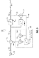
数ビット以上の分解能を有する信号帯域幅(fB)の2倍に等しい周波数又はそれを僅かに上回る周波数におけるサンプリングレート(fS)で信号を量子化する変換器は、従来、ナイキストレートコンバータとして知られている。従来のナイキストレートコンバータのアーキテクチャは、抵抗ラダー型回路網(例えば、R−2R回路網)を使用して実現されるアーキテクチャ、あるいはユニタリー(すなわち、均等)重み付け又は2進重み付けを有するスイッチ電流/電圧源を採用するアーキテクチャを含む。図1Aに示すような従来の抵抗ラダー型DACは、複数の2レベル(すなわち、デジタル)入力の2進重み付き和に等しい可変出力電圧を生成する。電圧加算演算は、適切に重み付けされた抵抗(すなわち、2進重み付き抵抗ラダー)を有する抵抗器の回路網を使用して実行される。抵抗回路網の出力における電圧は、バッファリングされ且つ/又は場合によってはアナログ・ローパスフィルタを使用して平滑化され、連続可変信号を生成する。別のDAC構造を図1Bに示す。これは、抵抗ラダー型回路網の代わりに電流源のスイッチバンクを使用してデジタル入力の2進重み付き和に等しい可変出力電流を生成する。図1Bに示すように、出力電流は、トランスインピーダンス増幅器(すなわち、電流−電圧変換器)を使用して比例出力電圧に変換される。 A converter that quantizes a signal at a sampling rate (f S ) at a frequency equal to twice the signal bandwidth (f B ) having a resolution of several bits or more or a frequency slightly higher than that is conventionally used as a Nyquist converter. Are known. Traditional Nyquist converter architectures are either implemented using a resistor ladder network (eg, R-2R network), or switch current / voltage with unitary (ie, equal) or binary weighting. Includes architectures that employ sources. A conventional resistive ladder DAC as shown in FIG. 1A produces a variable output voltage equal to a binary weighted sum of a plurality of two-level (ie, digital) inputs. The voltage addition operation is performed using a network of resistors having appropriately weighted resistors (ie, binary weighted resistor ladders). The voltage at the output of the resistor network is buffered and / or smoothed, possibly using an analog low pass filter, to produce a continuously variable signal. Another DAC structure is shown in FIG. 1B. This uses a switch bank of current sources instead of a resistor ladder network to produce a variable output current equal to the binary weighted sum of the digital inputs. As shown in FIG. 1B, the output current is converted to a proportional output voltage using a transimpedance amplifier (ie, a current-to-voltage converter).
従来のナイキスト変換器は、潜在的に非常に高い瞬時帯域幅を達成できるが、以下に更に詳細に説明するように、本発明者は、抵抗ラダー型回路網又はスイッチ電流源における構成要素の不整合により、取得可能な分解能を大きく制限する丸め誤差が発生する可能性があることを見出した。更に従来のナイキスト変換器の分解能は、サンプリングジッタ及び熱雑音等の他の実際の実現例の欠陥により制限される。ナイキスト変換器は、理論的に10GHzを上回る瞬時帯域幅で高い分解能を潜在的に実現できるが、上述の問題により、この潜在性は従来のナイキスト変換器において実現されていない。 While conventional Nyquist converters can potentially achieve very high instantaneous bandwidths, as will be described in more detail below, the present inventor has found that a component failure in a resistive ladder network or switch current source. We have found that matching can cause rounding errors that greatly limit the resolution that can be obtained. Furthermore, the resolution of conventional Nyquist converters is limited by other practical implementation deficiencies such as sampling jitter and thermal noise. Nyquist converters can theoretically achieve high resolution with instantaneous bandwidths in excess of 10 GHz, but due to the problems described above, this potential has not been realized in conventional Nyquist converters.
量子化雑音及び誤差を低減しようとする別の従来の方法は、オーバサンプリング技術を使用する。従来のナイキスト変換器は、各デジタル入力を単一の比例出力サンプル(すなわち、電圧又は電流)に変換する。従来のオーバサンプリング変換器は、疑似ランダム2値サンプル(すなわち、正数又は負数)のシーケンスの平均がデジタル入力に比例するように、まず各デジタル入力をこの2値疑似ランダムシーケンスに変換する。従って、オーバサンプリング変換器は、入力信号帯域幅の2倍より非常に高いレート(すなわち、fS)で(すなわち、fS>>fB)粗なアナログ電圧又は電流出力を生成する。ここで、従来、N=1/2・fS/fBは変換器のオーバサンプリング比と呼ばれる。デジタル入力に比例する連続可変出力は、出力サンプルを効果的に平均するローパスフィルタリング演算を使用して2値疑似ランダム出力シーケンスから生成される。この平均化処理においては、オーバサンプリング変換器の帯域幅が減少するが、量子化雑音(すなわち、連続可変信号を表すために2つの値のみを使用することにより発生する雑音)と、構成要素の不整合、サンプリングジッタ及び熱雑音の結果として得られる誤差とが軽減することにより変換器の分解能が向上するという利点を有する。この利点の範囲は、出力サンプリングレートfSに直接関連し(すなわち、利点はサンプリングレートの上昇と共に増加する)、従来、信号自体を減衰させずに信号帯域幅における誤差及び量子化雑音を理想的に減衰させるノイズシェーピング処理と共にオーバサンプリングを使用して拡げられる。量子化ノイズシェーピング処理及びそれに続くローパスフィルタリング(すなわち、出力平均化)により、オーバサンプリング変換器は、低分解能を有する高レート中間信号を改善された分解能を有する相対的に狭い帯域幅の出力信号に変換する。 Another conventional method that seeks to reduce quantization noise and errors uses oversampling techniques. A conventional Nyquist converter converts each digital input into a single proportional output sample (ie, voltage or current). Conventional oversampling converters first convert each digital input to this binary pseudorandom sequence so that the average of the sequence of pseudorandom binary samples (ie, positive or negative) is proportional to the digital input. Thus, the oversampling converter produces a coarse analog voltage or current output at a rate much higher than twice the input signal bandwidth (ie, f S ) (ie, f S >> f B ). Here, conventionally, N = 1/2 · f S / f B is called an oversampling ratio of the converter. A continuously variable output proportional to the digital input is generated from the binary pseudo-random output sequence using a low-pass filtering operation that effectively averages the output samples. In this averaging process, the bandwidth of the oversampling converter is reduced, but the quantization noise (ie, the noise generated by using only two values to represent a continuously variable signal) and the component This has the advantage that the resolution of the transducer is improved by reducing mismatches, sampling jitter and errors resulting from thermal noise. This range of benefits is directly related to the output sampling rate f S (ie, the benefits increase with increasing sampling rate) and has traditionally been ideal for error and quantization noise in the signal bandwidth without attenuating the signal itself. It can be extended using oversampling along with a noise shaping process that attenuates it. Through quantization noise shaping and subsequent low-pass filtering (ie, output averaging), the oversampling converter converts a high-rate intermediate signal with low resolution to a relatively narrow bandwidth output signal with improved resolution. Convert.
図2A及び図2Bは、従来のローパス・オーバサンプリング変換器5A及び5Bをそれぞれ示すブロック図である。典型的な従来のオーバサンプリング変換器は、一般に変換器オーバサンプリング比Nによるアップサンプリング6Aとその後のインターポーレーション(ローパス)フィルタリング6Bとからなるアップサンプリング演算6を採用し、量子化雑音を整形又は有色化するためにデルタ−シグマ(ΔΣ)変調器7A及び7Bを使用する。名前が示すように、デルタ−シグマ変調器7A及び7Bは、差分演算8(すなわち、デルタ)及び積分演算13A及び13B(すなわち、シグマ)を実行することにより2レベル量子化器10により発生される雑音を整形する。例えば、以下の式を実行する。
2A and 2B are block diagrams showing conventional low-pass / over-sampling
![]()
![]()
図2Aに示す変換器5Aは、インターポーレーション・ΔΣ変調器7Aと従来呼ばれるものを使用する。図2Bに示す誤差フィードバック構造を有する別のΔΣ変調器7Bは、変換器5Bにおいて使用される。D.Anastassiouの「Error Diffusion Coding In A/D Conversion」IEEE Transactions on Circuits and Systems、Vol.36、1989年を参照。一般にデルタ−シグマ変調器は、1つの伝達関数(STF)を有する信号及び異なる伝達関数(NTF)を有する量子化雑音を処理する。従来の伝達関数(すなわち、2レベル量子化器10の黙示的な遅延を考慮した後)は、STF(z)=z−1及びNTF(z)=(1−z−1)Pの形式である。ただし、z−1はTCLK=1/fCLKに等しい単位遅延を表し、Pは変調器の次数又はノイズシェーピング応答と呼ばれる。P=1を有するデルタシグマ変調器に対するSTF周波数応答30及びNTF周波数応答32を図2Cに示す。双方の回路5A及び5Bに対して、出力サンプリングレートfS、従って変換器のオーバサンプリング比Nは、デルタ−シグマ変調器7A及び7Bのクロック周波数fCLK(すなわち、図2A及び図2Bにおいて2レベル量子化器10に対する入力クロックとして示される)により判定される。
The
図2A及び図2Bに示すデルタ−シグマ変換器5A及び5Bは、従来、ローパス・デルタ−シグマ変換器として公知のものである。従来のローパス変換器に対する変形例は、バンドパス・デルタ−シグマ変調器を採用し、零を上回る周波数を中心とする狭帯域信号の変換を可能にする。図3Aに示す例示的なバンドパス・オーバサンプリング変換器40Aは、差分演算8(すなわち、デルタ)及び積分演算13C(すなわち、シグマ)をそれぞれ実行することにより2レベル量子化器10からの雑音を整形するバンドパス・デルタ−シグマ変調器42を含む。ここで、以下の式が成り立つ。
The delta-
![]()
![]()
図3Aに示す従来のバンドパスΔΣ変調器は、2次(すなわち、P=2)と考えられ、2レベル量子化器10の黙示的な遅延を考慮した後、STF(z)=z−1及びNTF(z)=1+z−2を有する。ただし、z−1はTCLKに等しい単位遅延を表す。実際のバンドパス・デルタ−シグマ変調器の雑音伝達関数(NTF)は、少なくとも2次応答である。ローパスの場合と同様に、バンドパスΔΣ変調器は量子化雑音応答71とは異なる図3Bに示す信号応答70を有する。図3Bに示すように、図3Aのバンドパス変調器は、変換器のナイキスト帯域幅(すなわち、1/4・fS)の中心で最小値72を有するNTFを有する。2レベル量子化10の後、標準的な従来のローパス・オーバサンプリング変換器(例えば、変換器5A及び5Bのいずれか)で実行されるフィルタリングと同様の量子化雑音のフィルタリング43が実行される。図3Aにおいて、入力データ(すなわち、デジタル入力)レートは変換器の出力サンプリングレートfCLKに等しいため、アップサンプリング演算は含まれない。しかし、入力データレートが変換器の出力サンプリングレートfCLKより低い場合、アップサンプリング演算は含まれる。
The conventional bandpass ΔΣ modulator shown in FIG. 3A is considered second order (ie, P = 2) and STF (z) = z −1 after considering the implicit delay of the two-
本発明者は、図2A及び図2Bに示すような従来のローパスΔΣ変換器及び図3Aに示すような従来のバンドパスΔΣ変換器が非常に高い瞬時帯域幅及び高分解能を必要とするアプリケーションにおいてそれらの有用性を制限するいくつかの欠点を有することを見出した。発明を実施するための形態の節で更に詳細に説明するこれらの欠点は、(1)整形量子化雑音及び誤差を減衰させるために使用される狭域ローパス又は狭域バンドパスフィルタリング演算により制限される変換帯域幅、(2)デルタ−シグマ変調器のクロック周波数fCLK(すなわち、2レベル量子化器のクロック周波数)により制限される分解能(SNDR)、(3)2レベル量子化器による安定した演算に必要な低次ノイズシェーピング応答(すなわち、一般にバンドパス変調器の場合は2次)により制限される分解能を含む。これらの欠点のために、(1)出力(平滑化)フィルタの量子化雑音減衰を向上するために帯域幅を減少せずに、あるいは(2)高次変調器が2レベル量子化により不安定であるためより高速な回路を使用して変換器のサンプリングレートを増加せずに、従来のオーバサンプリング変換器の分解能を増加することはできない。更に従来のオーバサンプリング変換器は、量子化雑音周波数応答が最小値である時の周波数(fnotch)を動的に変動、すなわち再プログラミングする手段を提供しないデルタ−シグマ変調器構造を採用する。しかし、本発明者は、プログラミングに依存して単一の変換器が異なる(複数の)周波数帯域で動作できるマルチモードの応用例(例えば、周波数合成器及び調整可能無線機)において、そのような特徴が有利であることを見出した。 The present inventor has found that the conventional low-pass ΔΣ converter as shown in FIGS. 2A and 2B and the conventional band-pass ΔΣ converter as shown in FIG. 3A require an extremely high instantaneous bandwidth and high resolution. It has been found that it has several drawbacks that limit their usefulness. These shortcomings, described in more detail in the Detailed Description section, are limited by (1) the narrowband lowpass or narrowband pass filtering operations used to attenuate shaped quantization noise and errors. (2) Resolution (SNDR) limited by the clock frequency f CLK of the delta-sigma modulator (ie, the clock frequency of the two-level quantizer), (3) Stable by the two-level quantizer It includes a resolution limited by the low order noise shaping response (ie, generally second order for bandpass modulators) required for the operation. Because of these drawbacks, (1) without reducing the bandwidth to improve the quantization noise attenuation of the output (smoothing) filter, or (2) the higher order modulator is unstable due to two-level quantization Thus, it is not possible to increase the resolution of a conventional oversampling converter without using a faster circuit to increase the sampling rate of the converter. Furthermore, conventional oversampling converters employ a delta-sigma modulator structure that does not provide a means to dynamically vary, ie, reprogram, the frequency (f notch ) when the quantization noise frequency response is at a minimum. However, in the multi-mode applications (eg frequency synthesizers and tunable radios) where the single converter can operate in different frequency bands depending on programming, such as We have found that the features are advantageous.
本発明は、特にナイキスト限界に接近する瞬時帯域幅及び非常に高いサンプリングレートで使用する改善されたDACを提供する。改善されたDACは、従来のナイキスト変換器の分解能制限と従来のオーバサンプリング変換器の帯域幅制限とを克服する。 The present invention provides an improved DAC, particularly for use with instantaneous bandwidths approaching the Nyquist limit and very high sampling rates. The improved DAC overcomes the resolution limitations of conventional Nyquist converters and the bandwidth limitations of conventional oversampling converters.
従って、本発明の特定の一実施形態は、離散時間量子化信号を連続時間連続可変信号に変換する装置であって、時間及び値に関して離散的な入力信号を受け入れる入力線と、入力線に結合された複数の処理ブランチと、加算器とを含む装置に関する。各処理ブランチは、(a)離散時間ノイズシェーピング/量子化回路、(b)離散時間ノイズシェーピング/量子化回路の出力に結合されたマルチビット−可変レベル信号変換器、(c)マルチビット−連続可変信号変換器の出力に結合されたアナログ・バンドパスフィルタを含む。加算器は、各処理ブランチにおけるアナログ・バンドパスフィルタの出力に結合される。処理ブランチのうちの異なる処理ブランチにおける離散時間ノイズシェーピング/量子化回路は、異なる周波数で変換雑音周波数応答最小値を有し、離散時間ノイズシェーピング/量子化回路の各々は、同一の処理ブランチにおけるアナログ・バンドパスフィルタにより選択された周波数帯域に対応する変換雑音周波数応答最小値を有する。なお、零周波数での変換(すなわち、DC)が望ましい応用例において、処理ブランチのうちの1つは、ローパス応答を生成するために零周波数を中心とするアナログ・バンドパスフィルタを含むのが好ましい。 Accordingly, one particular embodiment of the present invention is an apparatus for converting a discrete-time quantized signal into a continuous-time continuously variable signal, the input line accepting a discrete input signal with respect to time and value, and coupled to the input line The present invention relates to an apparatus including a plurality of processing branches and an adder. Each processing branch includes (a) a discrete-time noise shaping / quantization circuit, (b) a multi-bit to variable level signal converter coupled to the output of the discrete-time noise shaping / quantization circuit, and (c) multi-bit-continuous. It includes an analog bandpass filter coupled to the output of the variable signal converter. The adder is coupled to the output of the analog bandpass filter in each processing branch. Discrete-time noise shaping / quantization circuits in different processing branches of the processing branches have transform noise frequency response minima at different frequencies, and each of the discrete-time noise shaping / quantization circuits is analog in the same processing branch. It has a minimum conversion noise frequency response corresponding to the frequency band selected by the bandpass filter. Note that in applications where conversion at zero frequency (ie, DC) is desirable, one of the processing branches preferably includes an analog bandpass filter centered at zero frequency to produce a low pass response. .
一般にそのような装置は、従来の変換器により可能である分解能及び帯域幅より高い分解能及び高い帯域幅のより適切な組み合わせを提供でき、例えば種々の直接変換送信機、ソフトウェア無線又はコグニティブ無線、マルチチャネル通信送信機、全デジタルRADARシステム及び任意の高速波形発生器において種々の商業的、工業的及び軍事的応用例に使用される。 In general, such devices can provide a more appropriate combination of higher resolution and higher bandwidth than possible with conventional converters, such as various direct conversion transmitters, software defined radios or cognitive radios, It is used for various commercial, industrial and military applications in channel communication transmitters, all digital RADAR systems and any high speed waveform generator.
本発明の別の特定の一実施形態は、離散時間量子化信号を連続時間連続可変信号に変換する装置であって、時間及び値に関して離散的な入力信号を受け入れる入力線と、入力線に結合された入力を有し且つ複数の並列パスを有する離散時間ノイズシェーピング/量子化回路であり、そのような各並列パスが離散時間ノイズシェーピング/量子化回路により出力される完全な信号の異なるサブサンプリング位相を生成する離散時間ノイズシェーピング/量子化回路と、離散時間ノイズシェーピング/量子化回路の出力に結合されたマルチビット−可変レベル信号変換器と、マルチビット−連続可変信号変換器の出力に結合されたアナログ・バンドパスフィルタとを含む装置に関する。離散時間ノイズシェーピング/量子化回路は、アナログ・バンドパスフィルタにより選択された周波数帯域に対応する変換雑音周波数応答最小値を有する。 Another particular embodiment of the invention is an apparatus for converting a discrete-time quantized signal into a continuous-time continuously variable signal, the input line accepting a discrete input signal with respect to time and value, and coupled to the input line Discrete-time noise shaping / quantization circuit having a plurality of parallel paths, each such parallel path having a different sub-sampling of the complete signal output by the discrete-time noise shaping / quantization circuit A discrete-time noise shaping / quantization circuit for generating a phase, a multibit-variable level signal converter coupled to the output of the discrete-time noise shaping / quantization circuit, and an output of the multibit-continuous variable signal converter And an analog bandpass filter. The discrete time noise shaping / quantization circuit has a minimum converted noise frequency response corresponding to the frequency band selected by the analog bandpass filter.
本発明の別の特定の実施形態は、離散時間量子化信号を連続時間連続可変信号に変換する装置であって、時間及び値に関して離散的な入力信号を受け入れる入力線と、入力線に結合された第1の入力、第2の入力及び出力を有する加算器と、加算器の出力に結合されたマルチビット−可変レベル信号変換器と、マルチビット−連続可変レベル信号変換器の出力に結合されたアナログ・バンドパスフィルタと、加算器の出力に結合された入力を有し、出力を更に有し、且つ入力においてマルチビット信号の種々のビットを種々のマルチビットファクタで倍率変更する非線形ビットマッピング部と、非線形ビットマッピング部の出力に結合された入力及び加算器の第2の入力に結合された出力を有するフィードバックループフィルタとを含む装置に関する。 Another particular embodiment of the present invention is an apparatus for converting a discrete time quantized signal into a continuous time continuously variable signal, coupled to the input line and an input line that accepts a discrete input signal with respect to time and value. An adder having a first input, a second input and an output; a multi-bit to variable level signal converter coupled to the output of the adder; and an output of the multi-bit to continuously variable level signal converter. Non-linear bit mapping with an analog bandpass filter and an input coupled to the output of the adder, further having an output, and scaling the various bits of the multi-bit signal at the input by various multi-bit factors And a feedback loop filter having an input coupled to the output of the nonlinear bit mapping unit and an output coupled to the second input of the adder About.
上述の概要は、単に本発明の特定の態様を簡単に説明することを意図する。添付の図面と共に特許請求の範囲及び以下の好適な実施形態の詳細な説明を参照することにより、本発明を更に包括的に理解できる。 The above summary is merely intended to briefly describe certain aspects of the present invention. A more comprehensive understanding of the present invention can be obtained by reference to the claims and the following detailed description of the preferred embodiments in conjunction with the accompanying drawings.
以下の開示において、添付の図面を参照して本発明を説明する。ただし、図面は、本発明の特定の代表的で且つ/又は例示的な実施形態と特徴とを単に示すものであり、いかなる方法でも本発明の範囲を限定することを意図しないことが理解されるべきである。以下は、添付の各図面の簡単な説明である。 In the following disclosure, the invention will be described with reference to the accompanying drawings. It will be understood, however, that the drawings merely depict certain representative and / or exemplary embodiments and features of the invention, and are not intended to limit the scope of the invention in any way. Should. The following is a brief description of the accompanying drawings.
本発明に係る好適な変換器は、本明細書においてマルチチャネルバンドパスオーバサンプリング(MBO)と呼ばれることもある技術を使用する。従来のオーバサンプリングデジタル−アナログ変換器にある程度類似する方法において、MBO変換器は、量子化誤差、サンプリングジッタ及び熱雑音の分解能低下作用を緩和するノイズシェーピングと共に「オーバサンプリング」(この用語は本明細書において広範に使用される)の形態を採用する。本発明の好適な実施形態に係るMBO変換器は、以下の技術的革新のうちの1つ以上を取り入れて、瞬時帯域幅及び分解能を向上する。すなわち、(1)複数のオーバサンプリング変換器(例えば、各々が異なる周波数帯域を処理する)が並列に動作して、従来のオーバサンプリング変換器の帯域幅制限を克服する。(2)変調器の有効オーバサンプリング比が量子化器のクロック周波数fCLKに厳密に依存しないように、マルチレート(すなわち、ポリフェーズ)デルタ−シグマ変調器(好ましくは2次以上)が従来のデルタ−シグマ変調器の代わりに使用される。(3)2次より高い次数のノイズシェーピング応答による安定した動作を可能にするために、マルチビット量子化器が抵抗ラダー型回路網又は電流源回路網等のマルチビット−可変レベル信号変換器と共に使用される。(4)マルチビット−可変レベル信号変換器における不整合を補償するために(例えば、そのような不整合を模倣し、結果として得られる雑音が対応するバンドパス(再構成)フィルタにより除去される周波数範囲にその雑音を整形することにより)適応非線形ビットマッピングが使用される。(5)単一の変調器回路が任意の周波数帯域で動作するように構成されるのを可能にするために、マルチバンド(例えば、プログラマブルNTF応答)デルタ−シグマ変調器がシングルバンド(すなわち、固定NTF応答)デルタ−シグマ変調器の代わりに使用される。(6)標準的なアナログフィルタ構造に基づくアナログ信号再構成フィルタバンクが多くの振幅及び位相歪みを発生せずに変換雑音及び誤差を効果的に減衰させられるように、アナログ信号バンドパス(再構成)フィルタバンクにより発生する雑音及び歪みを解消するデジタル・プリディストーション・リニアライザ(DPL)が使用される。そのような技術の特定の組み合わせは、いくつかの点において、2つの別個の従来の技術、すなわち連続時間バンドパス・オーバサンプリングとマルチチャネル周波数インタリービングとを組み合わせる固有の新しい方法と考えられる。以下に更に詳細に説明するように、そのような技術を使用することにより、非常に高い瞬時帯域幅における制限された変換分解能及び精度の問題を克服できる。 A preferred converter according to the present invention uses a technique sometimes referred to herein as multi-channel bandpass oversampling (MBO). In a manner somewhat similar to a conventional oversampling digital-to-analog converter, the MBO converter is “oversampling” with noise shaping to mitigate the resolution degradation effects of quantization error, sampling jitter and thermal noise (this term is referred to herein). (Used extensively in writing). An MBO converter according to a preferred embodiment of the present invention incorporates one or more of the following technical innovations to improve instantaneous bandwidth and resolution. (1) Multiple oversampling converters (eg, each processing a different frequency band) operate in parallel to overcome the bandwidth limitations of conventional oversampling converters. (2) A multi-rate (ie polyphase) delta-sigma modulator (preferably second order or higher) is used so that the effective oversampling ratio of the modulator does not strictly depend on the quantizer clock frequency f CLK . Used instead of a delta-sigma modulator. (3) A multi-bit quantizer together with a multi-bit-variable level signal converter such as a resistor ladder network or a current source network in order to enable stable operation with a noise shaping response higher than the second order used. (4) To compensate for mismatches in multi-bit to variable level signal converters (eg, mimic such mismatches and the resulting noise is removed by a corresponding bandpass (reconstruction) filter) Adaptive nonlinear bit mapping is used (by shaping the noise to a frequency range). (5) To allow a single modulator circuit to be configured to operate in any frequency band, a multi-band (eg, programmable NTF response) delta-sigma modulator is single-band (ie, (Fixed NTF response) Used in place of a delta-sigma modulator. (6) Analog signal bandpass (reconstruction) so that an analog signal reconstruction filter bank based on a standard analog filter structure can effectively attenuate conversion noise and errors without generating much amplitude and phase distortion. ) A digital predistortion linearizer (DPL) is used that eliminates noise and distortion caused by the filter bank. A particular combination of such techniques is considered in some respects a unique new method that combines two separate conventional techniques: continuous time bandpass oversampling and multi-channel frequency interleaving. As described in more detail below, the use of such techniques can overcome the limited conversion resolution and accuracy problems at very high instantaneous bandwidths.
本発明の好適な実施形態に係る1つの変換器100の概略ブロック図を図4に示す。変換器100は、一般に周波数インタリービングの原理で動作し、離散時間入力信号102の全体の帯域幅が複数の小さいサブバンドに概念的に分離され(すなわち、細分され)、これらのサブバンドは(別個の処理ブランチにおいて)連続時間信号に個別に変換され、そしてこれらの信号が再度合成されて、入力信号と同一帯域幅の出力信号を生成する。前の文で「概念的」との用語を用いたのは、変換器100において、周波数帯域の分離が行われた後でのみ、連続時間信号への変換が行われるからである。しかし、その時点の前に、そのような最終的な周波数帯域の分離を予期して処理が実行される。
A schematic block diagram of one
従来のインタリーブ変換器において、インタリーブアレイにおける各サブ変換器は、細分された各帯域における信号帯域幅が減少しているため全体のサンプリングレートの約数で動作する。これに対して、本発明に係る変換器100は、各々が全体のサンプリングレートの約数ではなく全体のフルサンプリングレートで動作するのが好適であるM個の異なる周波数帯域を別個に処理する。この方法の結果、本明細書において「インタリーブ・オーバサンプリング比」又は「インタリーブファクタ」と呼ばれることもある有効オーバサンプリング比Mが得られる。なお、インタリーブファクタMは、従来のオーバサンプリング変換器の超過レートオーバサンプリング比Nとは異なるが、一般に変換雑音及び誤差に対して同一又は同様の効果を有する。
In a conventional interleaved converter, each subconverter in the interleaved array operates at a divisor of the overall sampling rate due to the reduced signal bandwidth in each subdivided band. In contrast, the
なお、特に指定のない限り、本明細書において「オーバサンプリング」という用語は広範な意味で使用され、信号又は信号のある部分が最終的に出力される信号又はその一部分より高いサンプリングレート(しかし、一般により低い分解能)での中間段階中にデジタル表現される処理技術を示す。本発明の好適な実施形態において、入力デジタル信号102は、異なるチャネル又はブランチ(例えば、ブランチ110及び120)で処理され、各々の目的は異なる周波数帯域を再生成することである。その後、そのようなチャネル又はブランチ110及び120の全ての出力は組み合わされ、最終的な出力信号135を提供する。以下に更に詳細に説明するように、各チャネル又はブランチ内の処理レートは、最終的にそのようなチャネル又はブランチから出力される対応する周波数帯域の帯域幅より高く、結果として有効オーバサンプリングを与える。
Unless otherwise specified, the term “oversampling” is used herein in a broad sense, and a signal or a portion of a signal is a higher sampling rate than the signal or portion of the signal that is ultimately output (but A processing technique that is digitally represented during an intermediate stage (generally lower resolution). In the preferred embodiment of the present invention, the input
図4を参照すると、変換器100は、M個の異なる周波数帯域の各々を処理するために別個のブランチ(例えば、ブランチ110又は120)を使用してデジタル(離散時間)入力信号102をM個の異なる周波数帯域として処理し、出力アナログ信号135を提供するために全てのブランチ出力を加算器131において合計する。本発明の一実施形態において、M個の異なる周波数帯域は、変換器100全体の出力データレートに対して直交するか又は少なくとも略直交する。より詳細には、信号102(一般に、マルチビット)は、例えば同一のデバイス内の別の回路からマルチビット信号を受信する内部ワイヤ、導電トレース又は同様の導電路として、あるいはマルチビット外部信号を受け入れる物理ポートとして実現される信号線103に入力される。
Referring to FIG. 4,
本実施形態において、デジタル入力信号102のサンプルは、まずデジタル・プリディストーション・リニアライザ(DPL)104に直接結合される。本明細書で使用されるように、「結合される」という用語又は他の形式の単語は、例えば前処理のために直接接続されること又は1つ以上の他の処理ブロックを介して接続されることを意味することを意図する。DPL104の1つの機能は、入力信号102を更なる処理のために十分な長さのワード長(例えば、最大16ビット)に変換することであるのが好ましい。DPL104の出力は、処理するためにM個の異なるブランチ(例えば、ブランチ110及び120)に分配される。各ブランチは、異なる周波数帯域に対応し、以下を含むのが好ましい。すなわち、(1)離散時間ノイズシェーピング/量子化回路(例えば、ノイズシェーパ及び量子化器112及び122)、抵抗ラダー型回路網113等のマルチビット−可変レベル信号変換器、並びにバンドパス(信号再構成)フィルタ(例えば、フィルタ115及び125)。最後に、加算器131は、それらM個のブランチの出力(より詳細には、信号再構成フィルタの出力)を合成し、最終的な出力信号135を生成する。説明を容易にするために、以下ではブランチ110の構成要素のみを参照して説明することが多いが、他のブランチ(例えば、ブランチ120)の各々においても同様の処理が行われることが好ましい。
In this embodiment, samples of the
本明細書で使用されるような「加算器」という用語は、例えば算術加算により及び/又は(単純にインバータを含むことで)算術減算により2つ以上の信号を組み合わせる1つ以上の回路を示すことを意図している。本明細書で使用されるような「加法により組み合わせる(additively combine)」という用語又はその変形表現は、算術加算又は減算を意味することを意図しており、一般に加算及び減算は信号の反転を使用することにより交換可能である。本明細書で使用されるような「バンドパス」という用語は、入力信号内で他の周波数と比較して所望の周波数帯域に対してより高い利得を提供するフィルタ又は他の回路を示す。ここで、所望の帯域は、零(この場合、ローパスフィルタと呼ばれる)又は他のあらゆる周波数を中心とすることができる。 The term “adder” as used herein refers to one or more circuits that combine two or more signals, eg, by arithmetic addition and / or by simple subtraction (by simply including an inverter). Is intended. As used herein, the term “additively combine” or variations thereof is intended to mean arithmetic addition or subtraction, and generally addition and subtraction use signal inversion. Can be exchanged. The term “bandpass” as used herein refers to a filter or other circuit that provides a higher gain for a desired frequency band compared to other frequencies in the input signal. Here, the desired band can be centered around zero (in this case called a low pass filter) or any other frequency.
DPL104の主な目的は、振幅及び位相歪み(すなわち、不完全な再構成)と、遅延スキューと、アナログ信号再構成フィルタバンク(バンドパスフィルタ115及び125と他の各ブランチにあるバンドパスフィルタとから構成される)により発生された位相歪みとを補償することである。図4に示す実施形態において、各離散時間ノイズシェーピング/量子化回路112はマルチビット出力(例えば、6〜8ビット)を有するが、単一ビットの出力を有する離散時間ノイズシェーピング/量子化回路112を使用することも本発明の範囲内である。いずれの場合においても、そのような各ノイズシェーピング/量子化回路112は、より複雑でない抵抗ラダー型回路網113(又は単一のマルチレベル連続時間信号への変換を行う他の構造)が使用されるように入力信号のワード長(及びそれに対応して分解能)を減少するのが好ましい。
The main objectives of
本実施形態において、各ノイズシェーピング/量子化回路112の一般的なマルチビット出力は、対応するノイズシェーピング/量子化回路112の出力が抵抗ラダー型回路網113(すなわち、R−2R)を介して変更された時に固定数の別個のレベル間で切り換わる単一の可変レベル信号に変換される。しかし、2進重み付き又はユニタリー重み付き電流源等の従来技術において公知の他のマルチビット−可変レベル信号変換器113が代わりに使用されてもよい。最後に、M個のチャネルが加算抵抗器を使用して加算器131において組み合わされるのが好ましいが、別の実施形態において、パッシブ及び/又はアクティブ信号の組み合わせ構造を含む種々の他の(例えば、他の従来の)アナログ加算器131のいずれかが代わりに使用されてもよい。
In this embodiment, the general multi-bit output of each noise shaping /
実質的に、好適な実施形態において、本発明は、2つの確立された技術、すなわちバンドパス・オーバサンプリング及び周波数インタリービングの変形例を組み合わせる新しい方法を介して高い瞬時帯域幅における制限された変換分解能及び精度の問題を克服する。各ノイズシェーピング回路が変換器のナイキスト帯域幅の特定の領域における変換雑音を最小限にするように複数のバンドパスノイズシェーピングチャネルを並列に組み合わせることにより、本発明は、高分解能及び高い瞬時帯域幅を同時に有する周波数インタリーブ変換器を提供できる。 In essence, in a preferred embodiment, the present invention provides a limited transform in high instantaneous bandwidth via a new method that combines two established techniques: bandpass oversampling and frequency interleaving variants. Overcome resolution and accuracy issues. By combining multiple bandpass noise shaping channels in parallel so that each noise shaping circuit minimizes conversion noise in a specific region of the converter's Nyquist bandwidth, the present invention achieves high resolution and high instantaneous bandwidth. Can be provided at the same time.
ノイズシェーピング及び量子化の検討事項
上述した実施形態において、ノイズシェーピング/量子化回路(例えば、112及び122)の各々は、図2A、図2B及び図3に示すものとは異なるように構築されるのが好ましい。好適な実施形態において、各処理ブランチ110又は120内の回路112又は122が効果、構築の容易さ及び構成の容易さの最適な組み合わせを達成することが分かっているため、本明細書においてマルチレート・デルタ−シグマ(μΔΣ)変調器と呼ばれる変更された誤差フィードバック構造は、そのような回路の変換ノイズシェーピング部分に使用される。なお、本発明の別の実施形態において、従来のデルタ−シグマ(ΔΣ)変調器を含む他の種類のノイズシェーピング回路を使用できる。いずれの場合においても、使用されるノイズシェーピング回路に対する主な検討事項は、非常に高いサンプリングレートにおいて安定した正確な動作を得られることが好ましいということである。従って、好適な実施形態に係る各ノイズシェーピング回路は少なくとも以下の3つの特性を有する。すなわち、(1)量子化/丸め誤差、サンプリング不確実性/ジッタ及び熱雑音に関連する性能低下等のノイズシェーピング回路の主な性能低下は、ノイズシェーピング応答の影響を受ける。(2)ノイズシェーピング回路は、4次以上のノイズシェーピング次数を有する安定した応答を生成する。(3)ノイズシェーピング回路の有効オーバサンプリング比は、構成要素の最大クロック周波数により制限されない。(4)NTFのヌルがプログラム可能パラメータ(例えば、ノイズシェーパ・フィードバックループフィルタ係数)の値により判定されるように、ノイズシェーピング回路はオールパス(又は少なくともほぼオールパス)信号伝達関数(STF)と帯域消去雑音伝達関数(NTF)とを有する。以下に更に詳細に説明するように、整形される雑音は、使用されるあらゆる量子化回路(例えば、回路112の内部にあり且つ図5に示す量子化回路114)により発生される雑音を含むが、マルチビット−可変レベル信号変換器113等の他の構成要素により発生される雑音を更に(又は代わりに)含む可能性がある。これらの特性を達成することは、一般にノイズシェーピング機能に対して従来のデルタ−シグマ変調器を使用することを含まない。
Noise Shaping and Quantization Considerations In the embodiments described above, each of the noise shaping / quantization circuits (eg, 112 and 122) are constructed differently than those shown in FIGS. 2A, 2B, and 3. Is preferred. In the preferred embodiment, it has been found that the
m=1のポリフェーズ分解ファクタの場合のマルチビット量子化回路114と組み合わせてプログラマブル・フィードバックループフィルタ150を採用する例示的なノイズシェーピング/量子化回路112の概略ブロック図を図5に示す。m=2のポリフェーズ分解ファクタの場合の例示的なμΔΣの概略ブロック図を図6に示す。一般に、本明細書で説明する実施形態は、組み合わせノイズシェーピング/量子化回路112を参照する。これを利用する理由は、特にm≧2の場合に量子化部をノイズシェーピング部から適切に分離するのが困難である可能性があるためである。しかし、実際には機能性は別個であり、特にm=1の時、例えば図5に示すようにそのような構成要素を別個に概念化するのが望ましい場合がある。
A schematic block diagram of an exemplary noise shaping /
従来のデルタ−シグマ(ΔΣ)変調器がオーバサンプリング比N=1/2・fS/fBを有する一方で、図5及び図6に示したマルチレート・デルタ−シグマ(μΔΣ)変調器は超過レートオーバサンプリング比N’=1/2・m・fS/fBを有する。ただし、mはμΔΣ変調器のポリフェーズ分解ファクタである。一般にμΔΣ変調器の回路計算量(量子化器114の数)はm2に比例して増加する。なお、μΔΣ変調器は、並列処理構造であるが、従来「並列」変調器と呼ばれることもある従来のMASH(すなわち、Multi−stAge SHaping)変調器とは異なる。MASH構造において、従来のΔΣ変調器は並列構成にグループ化され、NTFノイズシェーピング応答の次数Pを増加する。これに対して、μΔΣ変調器アーキテクチャは、ノイズシェーピング応答次数Pに関わらず有効オーバサンプリング比N’を増加する。 While the conventional delta-sigma (ΔΣ) modulator has an oversampling ratio N = 1/2 · f S / f B , the multi-rate delta-sigma (μΔΣ) modulator shown in FIGS. It has an excess rate oversampling ratio N ′ = 1/2 · m · f S / f B. Where m is the polyphase decomposition factor of the μΔΣ modulator. In general, the circuit calculation amount (the number of quantizers 114) of the μΔΣ modulator increases in proportion to m 2 . Note that the μΔΣ modulator has a parallel processing structure, but is different from a conventional MASH (ie, multi-stAge Shaping) modulator that is sometimes called a “parallel” modulator. In the MASH structure, conventional ΔΣ modulators are grouped in a parallel configuration to increase the order P of the NTF noise shaping response. In contrast, the μΔΣ modulator architecture increases the effective oversampling ratio N ′ regardless of the noise shaping response order P.
μΔΣ変調器において、図5において最も明確に示すように、信号141(加算器116から出力されて量子化器114に入力される)は遅延し(111B)(例えば、1fCLK周期だけ)、減算器117において信号146から減算される。結果として得られる組み合わせ信号145はフィルタ伝達関数H(z)を使用してフィルタリングされ(150)、その結果、信号147が得られる。最後に、信号147は加算器116において入力信号102と組み合わされる。同様の処理を図6に示すが、その実施形態において、μΔΣ変調器を構成する構成要素がm=2のポリフェーズ分解ファクタを実現するために複製されている。従って、図6のμΔΣ変調器212は同一のオーバサンプリング比Nの場合にfCLKレートの1/2で動作できるか、あるいは同一のfCLKレートの場合に2倍のオーバサンプリング比(すなわち、2・N)を達成できる。クロックレートを低減するために(すなわち、fCLKを低下するために)又は処理速度を増加するために(すなわち、Nを増加するために)ハードウェアを複製する処理は、従来技術においてポリフェーズ分解又はマルチレート処理と呼ばれることもある。
In the μΔΣ modulator, as shown most clearly in FIG. 5, the signal 141 (output from the
一般に、補正信号147を入力信号103に加算することにより、将来の量子化出力サンプル142は平均して前の量子化誤差を補償することが保証されるが、その一方で、そのような加算の前の量子化誤差の前処理は、量子化器114により発生された量子化雑音が現在の処理ブランチ(例えば、ブランチ110又は120)により処理されている入力信号の周波数帯域(すなわち、再構成フィルタにより処理された後に残る周波数帯域)から離れる方向にシフトされることを保証する。フィードバックループフィルタパラメータρの値に依存して、フィルタ150は、1/2・m・fCLKに等しい変換器のナイキスト帯域幅全体の選択された(例えば、所定の)周波数から離れる方向に変換雑音をシフトさせられる。
In general, adding the
μΔΣ変調器フィードバックループフィルタ150は、μΔΣ変調器雑音伝達関数(NTF)が所定の周波数(すなわち、フィードバックループフィルタパラメータρにより判定される周波数)でヌルを有する帯域消去応答を有するように、周波数に依存する遅延及び周波数に依存する振幅変動をフィードバック信号145に導入する。本実施形態において、フィードバックループフィルタ150は、乗算器118と、加算器119と、遅延レジスタ111Aとを使用して、周波数依存振幅変動及び周波数依存遅延の補正量を含む周波数応答を生成する。容易に理解されるように、乗算器118は、特にフィードバックループフィルタパラメータρが少ないデジタルビット数で表される(すなわち、ρの2進表現が殆ど項を含まない)場合、フィードバックループフィルタの計算量を潜在的に低減するために、シフト部及び加算部の組み合わせで置換される。本明細書で使用されるような「加算器」という用語は、例えば算術加算により及び/又は(単にインバータを含むことで)減算により2つ以上の信号を組み合わせる1つ以上の回路を示すことを意図する。本明細書で使用されるような「加法により組み合わせる」という用語又はその変形例は、算術加算又は減算を意味することを意図し、一般に加算及び減算は信号の反転を使用することにより交換可能であることが理解される。
The μΔΣ modulator
図5及び図6に示すように、μΔΣ変調器は、量子化器出力142に対する量子化器入力141の丸め精度(すなわち、精度又はビット幅)を低減する(図5を参照すると)マルチビット量子化回路114(又は図6における量子化回路214A〜214D)と共に実現されるのが好ましい。マルチビット量子化器114、更に好ましくは4ビット以上の精度を有するマルチビット量子化器114は、P>2の整形応答次数(すなわち、整形ファクタ)を有するμΔΣ変調器に対して安定した動作を保証することが分かっている。P≦2の整形ファクタの場合、変調器の安定性はマルチビット量子化器の使用に左右されないため、そのような実施形態において、図5及び図6に示したマルチビット量子化器は、特にm>1のポリフェーズ分解ファクタの場合に回路計算量を低減するために単一ビット(すなわち、2レベル)量子化器により置換されるのが好ましい。
As shown in FIGS. 5 and 6, the μΔΣ modulator reduces the rounding accuracy (ie, accuracy or bit width) of the
従来のΔΣ変調器のように、μΔΣ変調器は、1つの伝達関数(STF)を有する入力信号102と、異なる伝達関数(NTF)を有する変換雑音(例えば、図5を参照すると量子化器114からの)とを処理する。図5に示す回路を参照すると、量子化回路114の入力103と出力との間の線形信号伝達関数(STF)及び雑音伝達関数(NTF)は以下の通りである。
Like a conventional ΔΣ modulator, a μΔΣ modulator has an

従って、信号応答はオールパスであり、雑音応答はμΔΣフィードバックループフィルタ関数H(z)に依存する。変換器のナイキスト帯域幅にわたり所定の周波数で雑音ヌルを生成するために、フィードバックループフィルタ150は以下の形式の2次伝達関数を有するのが好ましい。
Therefore, the signal response is all-pass, and the noise response depends on the μΔΣ feedback loop filter function H (z). In order to generate a noise null at a predetermined frequency over the Nyquist bandwidth of the converter, the
![]()
![]()
ただし、ρはプログラム可能な値である。従って、雑音伝達関数は以下により与えられる。 Where ρ is a programmable value. Thus, the noise transfer function is given by:
雑音最小値の場所は、係数ρにより判定される。変換器の帯域全体にわたり雑音最小値を生成するために、ρは−2〜+2の範囲にわたり変動可能であるのが好ましい。特に以下の式に等しいρは、fに等しい周波数(すなわち、所定の処理ブランチのバンドパス周波数)で雑音最小値又はヌルを生成する。 The location of the minimum noise value is determined by the coefficient ρ. In order to generate a noise minimum over the entire bandwidth of the transducer, ρ is preferably variable over a range of −2 to +2. In particular, ρ equal to the following equation generates a noise minimum or null at a frequency equal to f (ie, the bandpass frequency of a given processing branch).
![]()
![]()
ただし、fCLKは量子化器のクロック周波数である。 Where f CLK is the quantizer clock frequency.
本発明の好適な実施形態に係るMBO変換器の有効オーバサンプリング比は、並列処理ブランチの数に等しいインタリーブ・オーバサンプリング比Mと1/2・m・fCLK/fBに等しい超過レートオーバサンプリング比N’との積に等しい。従って、MBO変換器の分解能性能は、並列処理ブランチ110の数Mを増加することにより(すなわち、ノイズシェーピング/量子化回路112の数を増加することにより)Nに関係なく増加される。しかし、処理ブランチは、出力信号再構成フィルタバンクにおけるアナログ・バンドパスフィルタ(例えば、フィルタ115及び125)の数を増加し且つそのような各フィルタ115の最低品質ファクタ(Q=fC/BW3dB)を同時に増加することで追加される。一般に、複数の高Qアナログフィルタを構築することに関連する設計計算量と結び付けられるフィルタバンクエイリアシング(又は他の歪み)の制御に関する問題により、変換器の有効オーバサンプリング比を増加するためにインタリーブファクタMを増加することは超過レートオーバサンプリング比N’を増加することより望ましくない。従って、MBO変換器は、超過レートオーバサンプリング比N’>1を有するのが好ましい。 The effective oversampling ratio of the MBO converter according to the preferred embodiment of the present invention is that the interleave oversampling ratio M equal to the number of parallel processing branches and the overrate oversampling equal to 1/2 · m · f CLK / f B Equal to the product of the ratio N ′. Therefore, the resolution performance of the MBO converter is increased regardless of N by increasing the number M of parallel processing branches 110 (ie, by increasing the number of noise shaping / quantization circuits 112). However, the processing branch increases the number of analog bandpass filters (eg, filters 115 and 125) in the output signal reconstruction filter bank and the minimum quality factor of each such filter 115 (Q = f C / BW3 dB). It is added by increasing at the same time. In general, the problem of controlling the filter bank aliasing (or other distortion) associated with the design complexity associated with building multiple high-Q analog filters causes the interleaving factor to increase the effective oversampling ratio of the converter. Increasing M is less desirable than increasing the overrate oversampling ratio N ′. Therefore, the MBO converter preferably has an excess rate oversampling ratio N ′> 1.
従来、オーバサンプリング比Nを増加することは、ノイズシェーピング変調器のfCLKレートを増加することにより実現される。しかし、上述したように、μΔΣ変調器の有効超過レートオーバサンプリング比N’はμΔΣ変調器のマルチレート(すなわち、ポリフェーズ)動作のためにfCLKにより制限されない。並列パスへのμΔΣ変調器のポリフェーズ分解により、変換器の有効サンプリングレート(fS)は変調器fCLKレートを増加せずに増加できる。例示する目的で、以下を有する図5に示すようなノイズシェーピング/量子化回路112を考察する。
Conventionally, increasing the oversampling ratio N is achieved by increasing the f CLK rate of the noise shaping modulator. However, as described above, the effective overrate oversampling ratio N ′ of the μΔΣ modulator is not limited by f CLK due to the multirate (ie, polyphase) operation of the μΔΣ modulator. Due to the polyphase decomposition of the μΔΣ modulator into a parallel path, the converter effective sampling rate (f S ) can be increased without increasing the modulator f CLK rate. For purposes of illustration, consider a noise shaping /
![]()
![]()
ノイズシェーピング/量子化回路112の量子化出力142 Q(y)は、以下の差分方程式により表される。
The quantization output 142 Q (y) of the noise shaping /
![]()
![]()
従って、最初の2つの出力サンプル(すなわち、n=0,1)に対する差分方程式は以下の通りである。 Thus, the difference equation for the first two output samples (ie, n = 0, 1) is as follows:
y1にy0を代入することにより、以下が得られる。 Substituting y 0 for y 1 gives:
これは以下の式に一般化される。 This is generalized to the following equation:
従って、Q(yn)は、上記例に対する入力及び他の全ての出力のみを使用して算出され、μΔΣ変調器が上記で示したポリフェーズ分解技術を使用する並列処理アーキテクチャ(すなわち、2つの並列パス)により具体化されることを実証する。すなわち、各並列パスの現在の出力は、ノイズシェーピング/量子化回路112全体に入力される信号、そのようなパス内で生成された信号及び/又は種々の他の並列パスからの先行する出力にのみ依存するが、他のあらゆる並列パスからの現在の出力には依存しない。上記例において、並列処理は、μΔΣ変調器が同一のオーバサンプリング比Nの場合にfCLKレートの1/2又は同一のfCLKレートの場合に2倍のオーバサンプリング比で実行することを可能にする。m=2のポリフェーズ分解ファクタの場合に上述したこのポリフェーズ分解方法は、より大きいポリフェーズ分解ファクタ及び任意のフィードバックループフィルタ関数(H(z))に拡張される。これは、特に高サンプリングレート変換器に対して重要な考慮事項である。図6は、上記の例毎にm=2のポリフェーズ分解ファクタを有するμΔΣ変調器を示す。上記で示したように、m≧2の時、各並列パスはブランチ110の離散時間ノイズシェーピング/量子化回路112により出力される完全な信号の異なるサブサンプリング位相を生成する。本明細書で使用されるように、「サブサンプリング位相」は、ファクタkによるサブサンプリングが行われるk個の可能な位相又は時間オフセットのうちの1つを示す。
Therefore, Q (y n ) is calculated using only the inputs and all other outputs for the above example, and the parallel processing architecture (ie, two two) where the μΔΣ modulator uses the polyphase decomposition technique shown above. It is demonstrated that it is embodied by a parallel path). That is, the current output of each parallel path is the signal input to the entire noise shaping /
図5及び図6に示す各μΔΣ変調器は2次ノイズシェーピング応答を有する。しかし、高次ノイズシェーピング応答は、低次ノイズシェーピング応答より入力信号の所望の周波数帯域(すなわち、対応するバンドパスフィルタ115又は125によりそれぞれ選択される現在の処理ブランチ110又は120に対する周波数帯域)から離れるように雑音をシフトし、それによりブランチのバンドパス(信号再構成)フィルタにより減衰される雑音量を増加するため、高次ノイズシェーピング応答は結果として改善された変換器の分解能性能を与える。例えば6次ノイズシェーピング応答の場合、図5に示すフィードバックループフィルタH(z)は以下の一般的な伝達関数を有する。
Each of the μΔΣ modulators shown in FIGS. 5 and 6 has a second-order noise shaping response. However, the higher order noise shaping response is derived from the desired frequency band of the input signal than the lower order noise shaping response (ie, the frequency band for the
従来、ノイズシェーピング回路係数(又はパラメータ)ρ0、ρ1及びρ2は等しい。すなわち、雑音伝達関数の零点が共通の周波数で発生する。根が等しい大きさを有する場合、結果として得られる雑音伝達関数は以下の式に簡略化される。 Conventionally, the noise shaping circuit coefficients (or parameters) ρ 0 , ρ 1 and ρ 2 are equal. That is, the zero point of the noise transfer function is generated at a common frequency. If the roots have equal magnitude, the resulting noise transfer function is simplified to
しかし、この簡略化された条件は、特に対応して少ない数のアナログ出力フィルタが存在する小さいインタリーブファクタ(M)の場合に出力雑音を最小限にすることに関して必ずしも最適である必要はない。雑音を最小限にする目的で等しくないNTF零点を有する高次変調器は、従来、「零点最適化」NTFを有するものとして示される。零点最適化NTFにより、NTF帯域消去応答の帯域幅は雑音ヌルの深度を減少することで増加される。インタリーブファクタMが小さい場合、この雑音応答における差分は、改善された変換器の分解能を与えられる。 However, this simplified condition need not necessarily be optimal with regard to minimizing output noise, especially in the case of a small interleave factor (M) where there is a correspondingly small number of analog output filters. Higher order modulators with unequal NTF zeros for the purpose of minimizing noise are conventionally shown as having “zero optimization” NTFs. With zero optimization NTF, the bandwidth of the NTF band cancellation response is increased by reducing the noise null depth. If the interleaving factor M is small, the difference in this noise response is given improved converter resolution.
しかし、μΔΣ変調器の場合、等しくない零点を有するNTFは、マルチレートアーキテクチャと関連する回路計算量を軽減できる。μΔΣ変調器等のフィードバック構造がポリフェーズ分解等の高周波数並列処理方法を使用して実現される場合、係数の動的な範囲の拡張は、NTF応答が好適なNTF応答から外れる原因となる。これは、ポリフェーズフィードバック構造において、入力値及び出力値が同一の係数(すなわち、ρ)と複数回乗算されて必要な算術精度を指数関数的に上昇させるために起こる。高精度な値を表すために多くのバイト数(すなわち、広いビット幅)が必要とされる。この結果として起こる計算量の増加は、無理係数すなわち単なる小数により表せない係数から等しい零点を有するNTFを近似するために単なる小数、好ましくは2進小数(すなわち、2の累乗である分母を有する小数)により表される有理係数から等しくない零点を有するNTFを使用することにより相殺される。単なる2進小数(例えば、3〜8ビット以下で表される値)により表される係数を使用することにより、μΔΣフィードバックループフィルタ乗算器は、加算器及び/又はビットシフト演算から成るより計算量の少ない回路により置換される。この計算量を軽減する技術は、本明細書において「ビット最適化」と呼ばれることもある本発明の新しい一態様である。従って、本発明の好適な実施形態において、ビット最適化NTFを有するμΔΣ変調器が採用される。なお、複雑さを軽減する目的の零点最適化(すなわち、ビット最適化)は、雑音除去のための従来の零点最適化とは異なる。しかし、ビット最適化の結果、NTFは等しい零点を有するNTFと比較して有益な応答を有する場合がある。 However, for μΔΣ modulators, NTFs with unequal zeros can reduce the circuit complexity associated with multirate architectures. When a feedback structure such as a μΔΣ modulator is implemented using a high frequency parallel processing method such as polyphase decomposition, the expansion of the dynamic range of coefficients causes the NTF response to deviate from the preferred NTF response. This occurs because in the polyphase feedback structure, the input and output values are multiplied multiple times by the same coefficient (ie, ρ) to increase the required arithmetic accuracy exponentially. A large number of bytes (ie, a wide bit width) is required to represent a highly accurate value. The resulting increase in computational complexity is simply a decimal, preferably a binary decimal (ie, a decimal with a denominator that is a power of 2) to approximate an NTF with equal zeros from an irrational coefficient, that is, a coefficient that cannot be represented by just a decimal. Is offset by using an NTF with unequal zeros from the rational coefficient represented by By using coefficients represented by simple binary decimals (eg, values represented by 3 to 8 bits or less), the μΔΣ feedback loop filter multiplier is more complex than an adder and / or a bit shift operation. It is replaced by a circuit with few. This technique of reducing computational complexity is a new aspect of the present invention, sometimes referred to herein as “bit optimization”. Accordingly, in a preferred embodiment of the present invention, a μΔΣ modulator having a bit optimized NTF is employed. Note that zero optimization (ie, bit optimization) for the purpose of reducing complexity is different from conventional zero optimization for noise removal. However, as a result of bit optimization, NTF may have a beneficial response compared to NTF with equal zeros.
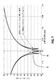
図7は、2つの例(1)ρ0=ρ1=ρ2=0.618034...となるような等しい零点を有する従来の6次ノイズシェーピング応答及び(2)ρ0=1/2、ρ1=5/8及びρ2=3/4を有するビット最適化された6次ノイズシェーピング応答に対する雑音伝達関数の比較を示す。図7に示すように、等しい零点を有する例示的なNTF80は、正規化周波数0.2Hzで90dBより大きい深度に到達する雑音ヌルを有し、その一方で、ビット最適化NTF81の深度は60dBをちょうど上回る深度に到達する。しかし、等しい零点を有するNTF80と比較すると、ビット最適化NTF81は、約55%広い(.025Hz対.016Hz)60dBの帯域幅を有する。少ない数Mの並列処理ブランチ(例えば、110及び120)を含むMBO変換器の場合、より小さい最大減衰量を有する広帯域NTFは、信号再構成フィルタ115の出力において、より大きい最大減衰量を有する狭帯域NTFより小さい雑音を与える。
FIG. 7 shows two examples (1) ρ 0 = ρ 1 = ρ 2 = 0.618034. . . Conventional 6th order noise shaping response with equal zeros such that and (2) bit optimized 6th order noise shaping with ρ 0 = 1/2, ρ 1 = 5/8 and ρ 2 = 3/4 A comparison of noise transfer function versus response is shown. As shown in FIG. 7, an
帯域外領域における量子化雑音のより大きい振幅により起こる量子化誤差がより速く蓄積されるため、高次ノイズシェーピング回路112を使用する場合、ノイズシェーパの出力が制限されたままであることを保証するために単一ビットより多いビットの量子化を使用するのが好ましい。その結果、図5及び図6に示す量子化器114はマルチビット量子化器であるのが好ましく、ノイズシェーピング応答は本発明の好適な実施形態において6次である。しかし、単一ビット量子化器(すなわち、比較器)及び低次ノイズシェーピング応答が代わりに使用でき、本発明の範囲内であると考えられるべきである。
In order to ensure that the output of the noise shaper remains limited when using the higher-order
バンドパス(信号再構成)フィルタの検討事項
本発明の好適な実施形態に係るMBO信号再構成において使用されるバンドパスフィルタ(例えば、フィルタ115及び125)に対する主な検討事項は、(1)設計計算量(フィルタ品質ファクタ及び次数に関して表されるのが好ましい)、(2)周波数応答(特に、ストップバンド減衰量)及び(3)振幅及び位相歪みである。最適な変換器の分解能性能は、一般にフィルタ次数の増加と共に増加する大きいストップバンド減衰量を示す周波数応答を有する変換雑音除去フィルタ(すなわち、バンドパス又は信号再構成フィルタ115)に対して取得される。更に、フィルタ応答は、デジタル・プリディストーション・リニアライザ(DPL)104の計算量を最小限にするために可能な限り少ない振幅及び位相歪みを発生させるのが好ましい。変換器インタリーブファクタ(M)を増加することにより実現される性能向上は、フィルタの3dBの帯域に対するフィルタ中心周波数の比(すなわち、fC/f3dB)として定義される再構成フィルタの品質ファクタの比例した増加に左右される。本発明の好適な実施形態に係るMBO変換器の場合、品質ファクタは再構成フィルタバンクにおける最大周波数フィルタに対して算出される(すなわち、fC=1/2fS)。従って、アナログフィルタ(例えば、フィルタ115及び125)に対する好適な品質ファクタは、変換器のインタリーブファクタに直接関連し、より好適にはMと等しい。現在、標準的な集中定数素子又は分布定数素子アナログフィルタに対する品質ファクタは約30に制限される。その結果、MBO変換器に対するインタリーブファクタに対する一般的な実際の制限はM?32である。しかし、32個のフィルタから成るアナログ再構成フィルタバンクと関連する計算量のために、本発明の好適な実施形態は、インタリーブファクタをM=16以下(すなわち、16個以下のアナログフィルタ115のバンク)に制限する。
Bandpass (Signal Reconstruction) Filter Considerations The main considerations for bandpass filters (eg, filters 115 and 125) used in MBO signal reconstruction according to the preferred embodiment of the present invention are: (1) Design Computational complexity (preferably expressed in terms of filter quality factor and order), (2) frequency response (especially stopband attenuation) and (3) amplitude and phase distortion. Optimal converter resolution performance is obtained for a transform denoising filter (ie, bandpass or signal reconstruction filter 115) having a frequency response that generally exhibits a large stopband attenuation that increases with increasing filter order. . In addition, the filter response preferably generates as little amplitude and phase distortion as possible to minimize the computational complexity of the digital predistortion linearizer (DPL) 104. The performance improvement achieved by increasing the converter interleave factor (M) is the quality factor of the reconstruction filter defined as the ratio of the filter center frequency to the 3 dB band of the filter (ie, f C / f 3 dB ). Depends on a proportional increase. For the MBO converter according to the preferred embodiment of the present invention, the quality factor is calculated for the maximum frequency filter in the reconstruction filter bank (ie, f C = 1 / 2f S ). Thus, the preferred quality factor for analog filters (eg, filters 115 and 125) is directly related to the interleave factor of the converter, and more preferably equal to M. Currently, the quality factor for standard lumped element or distributed element analog filters is limited to about 30. As a result, a general practical limit on the interleave factor for MBO converters is M? 32. However, due to the complexity associated with an analog reconstruction filter bank of 32 filters, the preferred embodiment of the present invention has an interleave factor of M = 16 or less (ie, a bank of 16 or less analog filters 115). ).
M=16のインタリーブファクタの場合、5次〜7次バターワースフィルタ応答は、変換雑音の十分なストップバンド減衰量を提供する。しかし、それらフィルタのバンクの全体の応答F(jω)は、周波数インタリーブアプリケーションにおける完全な信号再構成、すなわち小さい振幅及び位相歪みに必要な特性を示さない。しかし、本発明の好適な実施形態に係るシステムを使用すると、従来技術において一般に受け入れられている認識であるように、略完全な信号再構成はオールパス応答(すなわち、F(jω)=e−jnωt)を有するアナログフィルタバンクに厳密には依存しない。その代わり、フィルタバンク応答は、以下が成り立つようにデジタル・プリディストーション・リニアライザ(DPL)104(図4に示す)により実現される第2のフィルタ伝達関数L(z)との畳み込みにおいてオールパスであるのが望ましい。 For an interleave factor of M = 16, the 5th-7th Butterworth filter response provides sufficient stopband attenuation of the conversion noise. However, the overall response F (jω) of these filter banks does not exhibit the characteristics required for complete signal reconstruction, ie small amplitude and phase distortion, in frequency interleaved applications. However, using a system according to a preferred embodiment of the present invention, as is generally accepted in the prior art, a nearly complete signal reconstruction is an all-pass response (ie, F (jω) = e −jnωt It is not strictly dependent on an analog filter bank with Instead, the filter bank response is all-pass in convolution with a second filter transfer function L (z) implemented by a digital predistortion linearizer (DPL) 104 (shown in FIG. 4) so that Is desirable.
ただし、L(z)は物理的に実現可能な伝達関数(例えば、安定し且つ因果的である)である。この伝達関数L(z)を有する第2のフィルタは、追加された歪みがフィルタバンクの出力においてアナログ再構成フィルタバンク歪み(すなわち、バンドパスフィルタ115、125等の全てにわたる全体の歪み)を解消するように、追加された位相及び/又は振幅歪みにより入力信号102に対してプリディストーションを行う。上記式で表すように、フィルタ104は、上記式において係数βi及びαiによりそれぞれ表されるフィードフォワード成分及びフィードバック成分(好ましくは単純な重み付き遅延成分)の双方を採用するのが好ましい。特定のアナログフィルタバンクインパルス応答を最大に量子化するプリディストーション・リニアライザ104に対する係数βi及びαiは、連立1次方程式を解く従来の方法を使用して判定されるか、あるいは最小2乗平均(LMS)アルゴリズムを採用する技術等の従来の適応技術を使用して判定される。
Where L (z) is a physically realizable transfer function (eg, stable and causal). In the second filter with this transfer function L (z), the added distortion eliminates the analog reconstruction filter bank distortion at the output of the filter bank (ie, the overall distortion across all of the
軽減されたアナログフィルタバンクの計算量は、本発明の好適な実施形態が1つ以上のプリディストーション線形フィルタ104を採用する1つの理由である。第2の理由は、変換器のブランチ又はチャネル(例えば、ブランチ110及び120)間及びポリフェーズノイズシェーパ構成における並列パス間の伝播遅延差分に起因する信号スキューを補正するためにこの種のリニアライザ104が採用されるためである。
The reduced complexity of the analog filter bank is one reason why the preferred embodiment of the present invention employs one or more predistortion
デジタル・プリディストーション・リニアライザ104の計算量を低減するために、アナログフィルタバンクを構成するバンドパスフィルタ(例えば、フィルタ115及び125)に対する応答は、パスバンドリップル及び位相分散をそれぞれ生成する振幅及び位相歪みを最小限にするために選択されるのが好ましい。好適な実施形態において、振幅及び位相歪みを最小限にするために、個々のアナログフィルタバンク応答は、(a)周波数応答、(b)フィルタ次数、(c)中心周波数及び/又は(d)帯域幅に対して最適化されるのが好ましい。例えば均一に分布した中心周波数(すなわち、変換器のナイキスト帯域幅にわたり均一に分布した中心周波数)及び等しい帯域幅を有する5次バターワースフィルタから構成される従来のアナログフィルタバンクは、M=10のインタリーブファクタの場合に図8Aに示すように周波数応答のマグニチュード90を有する。図8Aに示すように、周波数応答のマグニチュード90は、負の方向に15dBを超え且つ正の方向に3dBを超えるパスバンドリップルを示す。あるいは、最適化された中心周波数、フィルタ次数及び帯域幅を有する3次ベッセル応答から成るアナログフィルタバンクは、図8Aに示すように周波数応答のマグニチュード91を有し、変換器のナイキスト帯域幅(M=10)にわたり±1dB未満のパスバンドリップルを示す。ベッセルフィルタバンクを構成する個々のフィルタ(例えば、フィルタ115及び125)に対する周波数応答のマグニチュードを図8Bに示す。
To reduce the computational complexity of the
ポリフェーズ分解技術は、デジタル・プリディストーション・リニアライザ(DPL)104にも適用可能であり、並列処理構造を形成し、DPL104を実現するために使用されるデジタル乗算器及び加算器のクロックレートを低下する。DPL104は、以下のデータ変換器入力シーケンスx(n)及びフィルタ係数l(n)の離散時間畳み込みを実行する伝達関数L(z)を有する再帰(すなわち、無限インパルス応答又はIIR)構造であるのが好ましい。
The polyphase decomposition technique can also be applied to the digital predistortion linearizer (DPL) 104, forming a parallel processing structure and reducing the clock rate of the digital multipliers and adders used to implement the
![]()
![]()
一般性を失わず、3つの係数(すなわち、β0、β1及びα1)と以下の伝達関数とを有するプリディストーション・リニアライザ104を仮定する。
Assume a
プリディストーション・リニアライザ104の動作は、以下の差分方程式により表される。
The operation of the
![]()
![]()
従って、最初の2つの出力サンプル(すなわち、n=1,2)に対する差分方程式は、以下の通りである。 Thus, the difference equation for the first two output samples (ie, n = 1, 2) is as follows:
![]()
![]()
y2にy1を代入すると以下が得られる。 Substituting y 1 for y 2 gives:
上記式は以下の式に一般化される。 The above formula is generalized to the following formula.
![]()
![]()
従って、ynは上記例に対する入力及び他の全ての出力のみを使用して算出され、μΔΣ変調器のように、デジタル・プリディストーション・リニアライザ104が2つの並列パス(すなわち、m=2のポリフェーズ分解ファクタ)を含む並列処理構造として実現されることを実証する。上記の例において、並列処理により、DPL104は変換器の入力データレートの1/2で実行することを可能にする。このポリフェーズ分解方法は、より大きいポリフェーズ分解ファクタ(すなわち、m>2)及び任意のプリディストーション・リニアライザ伝達関数(L(z))に拡張され、DPLが全体の変換器のサンプリングレートの約数で実行することを可能にする。並列パスへのポリフェーズ分解により、回路の複雑さがm倍以下だけ増加することで処理クロックレートが1/mに低下する。この回路の複雑さにおける不利益は、一般に非常に高いサンプリングレートの変換器の場合に好適な代替例である。図9は、3つの係数及びm=2のポリフェーズ分解ファクタを含むIIR伝達関数を有する例示的なデジタル・プリディストーション・リニアライザ104を示すブロック図である。従って、図9に示す例示的な回路は、全体の変換器のサンプリングレートの1/2で動作する。
Therefore, y n is calculated by using only the input and all the other output to the above example, as μΔΣ modulator,
マルチビット−可変レベル信号変換器の検討事項
本発明の好適な実施形態において、図4及び図5に示すノイズシェーピング/量子化回路112の2進重み付き出力は、変更された従来の抵抗ラダー型回路網を使用して単一の比例アナログ電圧レベルに変換される。しかし、電流源を含むマルチビット信号を単一の可変レベル出力に変換する他の従来の方法が代わりに使用されてもよく、本発明の範囲内であると考えられるべきである。本明細書において抵抗ラダー型回路網を参照するが、そのような参照は単なる例示であり、一般に他のあらゆるマルチビット−可変レベル信号変換器に対する参照と置換できることが理解されるべきである。
Multibit to Variable Level Signal Converter Considerations In the preferred embodiment of the present invention, the binary weighted output of the noise shaping /
特に、本発明の好適な実施形態は、バイポーラ動作のために変更されたR−2R抵抗回路網を使用する。ここで、Rはアナログフィルタ115の特性インピーダンスに整合される。一般にこのインピーダンスは、50オーム〜100オームである。図10は、VBIAS入力の追加によりバイポーラ動作のために変更された8つの入力を有する従来の抵抗ラダーを示す例示的な図である。
In particular, the preferred embodiment of the present invention uses a modified R-2R resistor network for bipolar operation. Here, R is matched to the characteristic impedance of the
抵抗ラダー型回路網に対する重要な検討事項は、構成抵抗素子の相対的な整合である。従来、完全な抵抗ラダーは、2進倍率に従って各デジタル入力を重み付けすることによりアナログ出力を作成することが理解される。ラダーの抵抗素子における不整合はこの2進倍率を歪ませ、非線形応答を生成する。この非線形応答は、出力波形を歪ませるため、変換されたアナログ信号の品質を低下する。抵抗ラダー型回路網を採用する従来の変換器において、抵抗素子に対する整合に関する要求(ε)は、以下の式に従って変換器の精度により判定される。 An important consideration for resistive ladder networks is the relative matching of the constituent resistive elements. Traditionally, it is understood that a perfect resistance ladder creates an analog output by weighting each digital input according to a binary scale factor. Mismatches in the ladder resistance elements distort this binary magnification and produce a non-linear response. This non-linear response distorts the output waveform, thus degrading the quality of the converted analog signal. In a conventional converter that employs a resistance ladder network, the requirement (ε) for matching the resistance element is determined by the accuracy of the converter according to the following equation:
![]()
![]()
ここで、上記式におけるBはビットでの変換器の有効分解能である。従って、8ビットの有効分解能の場合、要求される抵抗ラダーの整合性は〜0.2%である。 Where B in the above equation is the effective resolution of the converter in bits. Therefore, for an effective resolution of 8 bits, the required resistance ladder consistency is ˜0.2%.
本発明の好適な実施形態に係るMBO変換器のオーバサンプル動作は、抵抗ラダー型回路網に基づく従来の変換器にわたり2つの利点を与える。1つの利点は、ノイズシェーピング及びフィルタリングのために、オーバサンプル変換器は非オーバサンプル変換器と同一の有効分解能を達成するためにより少ない入力を有する抵抗ラダーを必要とする。従って、オーバサンプリングは抵抗ラダー型回路網の全体の計算量を低減する。要求される抵抗ラダーの入力数の減少は、変換器の有効オーバサンプリング比(N’xM)と、ノイズシェーピング/量子化回路112内のμΔΣ変調器のノイズシェーピング次数(P)と、信号再構成フィルタ115のストップバンド減衰量との関数である。抵抗回路網の複雑さを軽減し、必要とされるデジタル入力数を減少するために、本発明の好適な実施形態は8つ以下の入力(すなわち、各処理ブランチにおける抵抗ラダー型回路網に対する8つ以下のデジタル入力)を含む抵抗ラダー型回路網を使用する。
The oversampled operation of the MBO converter according to the preferred embodiment of the present invention provides two advantages over conventional converters based on resistor ladder networks. One advantage is that due to noise shaping and filtering, the oversample converter requires a resistor ladder with fewer inputs to achieve the same effective resolution as the non-oversample converter. Thus, oversampling reduces the overall computational complexity of the resistor ladder network. The required reduction in the number of resistor ladder inputs includes the converter effective oversampling ratio (N ′ × M), the noise shaping order (P) of the μΔΣ modulator in the noise shaping /
より重要な第2の利点は、オーバサンプリングにより、抵抗ラダー型回路網113における不整合により発生する歪みがノイズシェーピング/量子化回路112により整形され、例えば図11に示すように非線形ビットマッピングを含むことにより変換雑音フィルタ115により多くが除去されることである。オーバサンプリング変換器は、変換雑音及び歪みを整形するために誤差フィードバックを採用する。しかし、従来のオーバサンプリング方式において、抵抗ラダー型回路網の出力は、ノイズシェーピング回路フィードバックパスの一部ではない。従って、従来、抵抗ラダー型回路網113の不完全な2進倍率により起こる歪みは整形されない。本発明の好適な実施形態に係るMBO変換器は、図11に示すようにμΔΣ変調器フィードバックループに非線形ビットマッピング161を含む。非線形ビットマッピング161の目的は、抵抗ラダー型回路網113の非線形効果(すなわち、不整合)が効果的にμΔΣ変調器フィードバックパスの一部になるように(すなわち、信号145Bが抵抗ラダー型回路網113の出力から実際に発生したかのように)それら不整合を模倣することである。これは、変調器フィードバックパスにおけるデジタル分解能のレベル(すなわち、ビット幅>nビット)がノイズシェーピング/量子化回路112の出力におけるデジタル分解能のレベルより大きい(すなわち、ビット幅=nビット)ため可能である。すなわち、量子化器114からの各ビット出力(すなわち、ビットb0〜bn−1の各々)がマルチビットファクタ(C0〜Cn−1のそれぞれ)と乗算され、分解能を1ビットから複数ビットに増加するのが好ましい。フィードバックループフィルタ150を介して信号145Bを加算器116に供給する前に量子化器114からのそのようなビット出力毎に相対的に高い分解能の重みファクタを使用することにより、抵抗ラダー型回路網(又は他のマルチビット−可変レベル信号変換器)の2進倍率不完全性をより正確に整合できる。
A more important second advantage is that oversampling causes distortion caused by mismatch in the
より正確には、図11に示す非線形ビットマッピング係数C0...Cn−1は、抵抗ラダー型回路網113の抵抗素子における不整合により生成される2進倍率オフセットと一致するビットに依存する2進倍率オフセットを生成するように設定されるのが好ましい。ラダー型回路網113における抵抗器が完全に整合する場合、非線形ビットマッピング係数は、完全な2進重み付けを反映するのが好ましい(すなわち、C2=2・C1=4・C0)。反映しない場合、係数重み付けは近似的に2進であり、μΔΣ変調器の変換雑音が入力信号に対して付加的であるため、係数及び実際の抵抗回路網113の重み付けが完全に調整される場合、再構成フィルタ115の出力における変換雑音レベルは最小値である。従って、例えばアナログ2乗部162(図11に示すような)、あるいはアナログ絶対値部又はアナログ信号強度の他のセンサを低周波数アナログ−デジタル変換器163と共に使用して信号再構成フィルタ115の出力における信号レベル(又は強度)を検知することにより、処理ブロック164内の適応デジタル制御アルゴリズムを使用して最小変換雑音及び歪みに対する非線形ビットマッピング係数C0...Cn−1を調整できる。図11に示す回路160に対して、再構成フィルタ115の出力におけるレベル(ブロック162で判定されるような)に基づいて、処理ブロック164内のアルゴリズムは、非線形ビットマッピング係数C0...Cn−1と実際の抵抗ラダー113の重みファクタとの間の不整合を補正する制御信号165を生成するのが好ましい。最小2乗平均(LMS)等の従来の技術は、上述したデジタル校正ループ内の非線形ビットマッピング係数C0...Cn−1を適応するために処理ブロック164内で使用されてもよい。
More precisely, the nonlinear bit mapping coefficients C 0 . . . C n−1 is preferably set to generate a binary scale offset that depends on a bit that matches the binary scale offset generated by the mismatch in the resistive elements of
実際には、非線形ビットマッピング係数C0...Cn−1は、開始時に一度校正され(例えば、既知の信号を使用して)、その後、抵抗値の変化(例えば、熱変化による)を考慮するためにリアルタイムで動的に調整されるのが好ましい。好適な実施形態において、そのような動的な調整は、あらゆる変化の影響を評価するために十分な時間を与えるように約1秒に1回行われる。 In practice, the nonlinear bit mapping coefficients C 0 . . . C n−1 is calibrated once at the start (eg, using a known signal) and then dynamically adjusted in real time to account for resistance changes (eg, due to thermal changes). Is preferred. In the preferred embodiment, such dynamic adjustments are made about once every second to provide sufficient time to assess the impact of any change.
図11には示さないが、特定の実施形態において、入力信号102の変更の結果起こる出力電力のあらゆる変化を考慮に入れるために、デジタル入力信号102は適応制御モジュール164に供給される。一方、入力信号102の電力の変動が評価期間にわたり且つ/あるいは1つの評価期間から次の評価期間までに零に平均されると予想される実施形態において、適応制御モジュール164における決定は、ブロック162(図11に示すような)において測定された平均変換器出力電力にのみ基づいて行われるか、あるいはバンドパスフィルタ115から出力される信号の強度の他の何らかの尺度に基づいて行われる。
Although not shown in FIG. 11, in certain embodiments, the
従来のラダー型変換器の場合、ラダー型回路網における抵抗器の整合精度は変換器の精度を判定する。これに対して、好適なMBO変換器の精度は、変換器のオーバサンプリング比(NxM)と、μΔΣ変調器のノイズシェーピング応答次数(P)と、再構成フィルタ115のストップバンド減衰量との関数である。従って、オーバサンプリングにより、高精度変換器は低精度抵抗ラダー型回路網113を使用して実現可能になる。本発明の好適な実施形態は、わずか1%以上の精度の抵抗ラダー型回路網を使用して、非線形ビットマッピング部の必要とされる調整範囲を縮小する。
In the case of a conventional ladder type converter, the matching accuracy of the resistors in the ladder type network determines the accuracy of the converter. In contrast, the preferred MBO converter accuracy is a function of the converter oversampling ratio (N × M), the noise shaping response order (P) of the μΔΣ modulator, and the stopband attenuation of the
変換器全体の検討事項
デジタル・プリディストーション・リニアライザ(DPL)104とノイズシェーピング/量子化回路112内のμΔΣ変調器とは、マルチレート(ポリフェーズ)構造として実現可能であるため、図4に示す(マルチレートDPL104及びマルチレートノイズシェーピング/量子化回路112を含むより具体的で詳細な実施形態を図12に示す)変換器技術の瞬時帯域幅は、抵抗ラダー型回路網113を駆動するデジタル出力バッファの最大スイッチングレート及びアナログ再構成フィルタ(例えば、フィルタ115及び125)によってのみ制限される。
Considerations for the entire converter The digital predistortion linearizer (DPL) 104 and the μΔΣ modulator in the noise shaping /
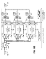
本発明の好適な実施形態に係るm=2のポリフェーズ分解ファクタを有するμΔΣ変調器を含むノイズシェーピング/量子化回路112を採用するMBO変換器の例示的なブロック図を図13A〜図13Cに示す。図13A〜図13Cの各々において、各ノイズシェーピング/量子化回路112A〜112Cの2つのマルチレート出力を組み合わせるために異なる構造が提供される。また、図13A〜図13Cの各々において、抵抗回路網は、代表的なMBO処理ブランチの出力を組み合わせるためにアナログ加算器として使用される。しかし、リアクティブ回路(例えば、ウィルキンソン回路、ランゲ回路等)及び/又はアクティブ回路に基づくような他の種類のアナログコンバイナが本発明の範囲内で考えられるべきである。図13Aにおいて、各ノイズシェーピング/量子化回路112A〜112Cは、ポリフェーズ分解ファクタm=2であるために2つのマルチレート出力を有する。各ノイズシェーピング/量子化回路112A〜112Cの2つのマルチレート出力は、ノイズシェーピング/量子化回路112A〜112Cのマルチレート出力を交互に順次選択する対応するマルチプレクサ172A〜172Cを使用して組み合わされ、これにより単一のデータストリームを対応する抵抗ラダー型回路網113A〜113Cに提供する。例えばマルチプレクサ172Aは、第1の周期でノイズシェーピング/量子化回路112Aの第1のマルチレート出力を抵抗ラダー型回路網113Aに結合し、第2の周期でノイズシェーピング/量子化回路112Aの第2のマルチレートパス出力を抵抗ラダー型回路網113Aに結合し、第3の周期でノイズシェーピング/量子化回路112Aの第1のマルチレートパス出力を抵抗ラダー型回路網113Aに結合する。以下に詳細に説明する別の方法と関連する欠点のために、各ノイズシェーピング/量子化回路112A〜112Cのマルチレート出力を組み合わせるために多重化を使用することは好ましい。
Exemplary block diagrams of an MBO converter employing a noise shaping /
図13Bは、各ノイズシェーピング/量子化回路112A〜112Cの2つのマルチレート出力を組み合わせるための別の構造を示す。図13Bにおいて、各ノイズシェーピング/量子化回路112A〜112Cのマルチレート出力は、加算回路176A〜176C(ノイズシェーピング/量子化回路112A〜112Cの出力と抵抗ラダー113A〜113Cへの入力との間)が後続する対応する逆移動平均(IMA)フィルタ174A〜174C(DPL104とノイズシェーピング/量子化回路112A〜112Cへの入力との間)を使用して組み合わされる。図示するように、各加算回路176A〜176Cは、マルチレート出力毎のクロックラッチと、ラッチ出力を組み合わせる加算器とを含む。各加算回路176A〜176Cのラッチは、ラッチ出力が定期的に順次更新されるようにクロック制御される。加算回路の各ラッチの出力は1/m・fCLKレートで更新され、ラッチの出力は互いに対して時間的に1/m・(1/fCLK)だけオフセットされるのが好ましい。ここで、mはμΔΣ変調器のポリフェーズ分解ファクタである(すなわち、図13Bにおいてはm=2)。ポリフェーズ分解ファクタm=2に対する図13Bに示す例示的な実施形態の場合、各加算回路176A〜176Cのラッチの出力は1/2・fCLKクロックの逆位相で更新される。従って、各加算回路176A〜176Cの加算器の出力はfCLKレートで更新される。従って、デジタル出力論理のスイッチング速度を減少するために、加算器は、例えば抵抗又はリアクティブコンバイナ回路網(例えば、y型スプリッタ、ウィルキンソンコンバイナ)を使用してアナログ(すなわち、連続時間)加算器として実現される。
FIG. 13B shows another structure for combining the two multi-rate outputs of each noise shaping /
図13Bの構造に類似する構造を図13Cに示す。図13Cにおいて、IMAフィルタ174A〜174Cは各ブランチにおいて使用されるが、各ノイズシェーピング/量子化回路112A〜112Cに対する各マルチレート出力は、抵抗ラダー型回路網を使用して単一の可変レベル信号に別個に変換され、所定のノイズシェーピング/量子化回路112A〜112Cに対するそのようなマルチレート出力の全てがアナログ加算器を使用して組み合わされるか又は加算される。一般に以下の説明は図13Bに示す回路を参照するが、同一の考慮事項が図13Cに示す回路にも当てはまる。
A structure similar to that of FIG. 13B is shown in FIG. 13C. In FIG. 13C, IMA filters 174A-174C are used in each branch, but each multirate output for each noise shaping /
入力IMAフィルタ174A〜174Cの目的は、アナログ加算部176A〜176C(又は図13Cに示す対応する加算構造)により発生されたsin(x)/x応答を補償することである。それらアナログ加算部は、図示する目的で図13Bでは別個のエンティティとして示されるが、抵抗素子を使用して実現され、抵抗ラダー型回路網と一体化される。出力多重化方法と比較して、この出力加算方法は、デジタル出力バッファ(ラッチ)のスイッチングレートが減少されるという利点を有する。しかし、出力加算方法は、大きいインタリーブファクタM及び大きいポリフェーズ分解ファクタmの場合に回路の複雑さを非常に増加する可能性のある複数のクロック位相(例えば、φ0及びφ1)を含むデジタルインタフェースと追加のフィルタ(すなわち、伝達関数D(z)を有するIMAフィルタ174A〜174C)とを使用する。また、更に詳細に以下に説明するように、有限ワード長の効果により、IMAフィルタリング174A〜174C(すなわち、D(z))がm>2のポリフェーズ分解ファクタに対する加算部のsin(x)/x応答を完全にオフセットするのを防止する。これらの理由のために、出力加算方法は、m=2のポリフェーズ分解ファクタの場合にのみ又は変換器出力スペクトルにおけるsin(x)/xヌルを許容できる応用例においてのみ使用されるのが好ましい。
The purpose of the input IMA filters 174A-174C is to compensate the sin (x) / x response generated by the
図13Bに示すようなノイズシェーピング/量子化回路112A〜112Cのマルチレート出力を組み合わせるために加算を使用することは、MBO変換器出力サンプルに移動平均フィルタ(すなわち、sin(x)/x応答を含む)を適用することと同等である。この移動平均フィルタは以下の形式の伝達関数を有する。
Using summation to combine the multirate outputs of noise shaping /
![]()
![]()
ただし、mはノイズシェーピング/量子化回路112A〜112Cからのマルチレート出力数と等しいポリフェーズ分解ファクタである(すなわち、図13Bではm=2)。移動平均フィルタの周波数応答は、mに依存してMBO変換器の出力データレートの約数でスペクトルヌルを有する。従って、加算部176A〜176Cの移動平均応答を取消すために、対応するIMAフィルタ174A〜174C(図13Bにおいて各ノイズシェーピング/量子化回路112A〜112Cの前に示す)は、以下により与えられる逆伝達関数を有するべきである。
However, m is a polyphase decomposition factor equal to the number of multi-rate outputs from the noise shaping /
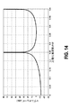
m=4のポリフェーズ分解ファクタの場合のIMAフィルタの周波数応答が図14に示され、1/4・fSで無限のマグニチュードを有する。ここで、fSは変換器の出力データレートである。その結果、有限利得(すなわち、デジタルフィルタに対する有限ワード長)を有するIMAフィルタ174A〜174Cは、μΔΣ変調器の出力において加算(すなわち、移動平均)部176A〜176Cにより生成されるヌルを完全に補償できない。一般に、移動平均応答は、1/m・fSに等しい周波数でそのようなスペクトルヌルを生成する。これは、m=2のポリフェーズ分解ファクタの場合に移動平均応答におけるスペクトルヌルがナイキスト周波数で発生することを意味し、これは、全体の変換器の帯域幅に関して殆ど又は全く重要でないMBO変換器の出力から削除可能である。従って、加算部を使用してノイズシェーピング/量子化回路112A〜112Cのマルチレート出力を組み合わせることは、最大2つのマルチレート出力(すなわち、m=2)を組み合わせる場合にのみ好ましい。
The frequency response of the IMA filter for a polyphase decomposition factor of m = 4 is shown in FIG. 14 and has an infinite magnitude at 1/4 · f S. Where f S is the output data rate of the converter. As a result, IMA filters 174A-174C with finite gain (i.e., finite word length for the digital filter) fully compensate the nulls produced by summing (i.e., moving average)
図15に示すように、多重化及び加算はノイズシェーピング/量子化回路112A〜112Cのマルチレート出力を組み合わせるハイブリッド構成において共に使用できる。m=4の例示的なポリフェーズ分解ファクタの場合の図15に示すこのハイブリッド方法は、多重化172を使用して最後の2つ以外の全てのマルチレート出力を組み合わせ、加算176A〜176Cを含むIMAフィルタ174A〜174Cを使用して(すなわち、この例においては追加の抵抗ラダー型回路網ではなくアナログ加算器を使用して)最後の2つのマルチレート出力を組み合わせる。従って、各ノイズシェーピング/量子化回路112A〜112Cに対する全体のポリフェーズ分解ファクタがm=4であっても、IMAフィルタ174A〜174C及び加算部176A〜176Cはm=2のポリフェーズ分解ファクタに基づいて動作する。このハイブリッド方法は、結果として、IMAフィルタ174A〜174Cの応答と加算部176A〜176Cの移動平均応答との間の不整合による性能の低下なしでMBO変換器の出力データレートを2倍に増加させる。なお、ノイズシェーピング/量子化回路112A〜112Cのマルチレート出力を組み合わせる上述した方法のいずれも高次マルチプレクサ又は高次微分器及び加算器を使用して多くのマルチレート出力(すなわち、大きいポリフェーズ分解ファクタm)に一般化される。
As shown in FIG. 15, multiplexing and summing can be used together in a hybrid configuration that combines the multi-rate outputs of noise shaping /
上述したいくつかの実施形態は、IMAフィルタ174A〜174Cとデジタル・プリディストーション・リニアライザ(DPL)104とを含む。しかし、別の実施形態において、これらの異なるフィルタリング機能は単一の構造に含まれる。 Some of the embodiments described above include IMA filters 174A-174C and a digital predistortion linearizer (DPL) 104. However, in another embodiment, these different filtering functions are included in a single structure.
MBO変換器技術(例えば、図4に示すような)の瞬時帯域幅は、抵抗ラダー型回路網113又は2進重み付きデジタル信号を比例アナログ電圧レベルに変換するのに使用される他の回路網に結合されるデジタル出力バッファ(又はラッチ)のスイッチングレートによってのみ制限される。デジタル出力バッファは、CMOS集積回路処理技術において10GHzを超えるスイッチング速度で商業的に実証されている。マルチレート出力を組み合わせるための先行するハイブリッド方法を使用する場合、例えばこの容量は最大20GHzの全体の変換器のサンプリングレートfS及び10GHzを超える対応する瞬時帯域幅に変換される。
The instantaneous bandwidth of MBO converter technology (eg, as shown in FIG. 4) can be achieved by using
しかし、上述したように、MBO変換器100の分解能性能は、サンプリングレートfSにより制限されず、インタリーブファクタ(すなわち、並列処理ブランチの数M)と、μΔΣ変調器ノイズシェーピング次数と、バンドパス(再構成)フィルタ115の特性との関数である。更に、従来のオーバサンプリング変換器のように、MBO変換器技術は、他の高速変換器アーキテクチャの性能を低下させるクロックジッタ及び熱雑音等の欠陥の影響を相対的に受けないように実現される。特に、クロックジッタ及び量子化器熱雑音等の欠陥は、量子化雑音と同様の方法でノイズシェーピング応答の影響を受けるようにされ、アナログ・バンドパス(再構成)フィルタ(例えば、フィルタ115及び125)による大きな減衰を可能にする周波数応答を示す。
However, as described above, the resolution performance of the
MBO変換器100に対するシミュレートされた分解能性能結果は、6次ノイズシェーピング応答、種々のインタリーブファクタM及び種々のアナログ再構成フィルタ115の次数に対する表1に示される。
The simulated resolution performance results for the
システム環境
一般に、明示的に示さない限り、本明細書で説明するシステム、方法、機能性及び技術の全ては、1つ以上のプログラマブル汎用コンピューティングデバイスを使用して実現される。一般にそのようなデバイスは、例えば共通バスを介して相互接続される以下の構成要素、すなわち1つ以上の中央処理装置(CPU)と、読み出し専用メモリ(ROM)と、ランダムアクセスメモリ(RAM)と、他のデバイスとインタフェースする(例えば、シリアルポート、パラレルポート、USB接続又はFirewire接続等のハードワイヤード接続を使用するか又はBluetooth(登録商標)又は802.11プロトコル等の無線プロトコルを使用して)ための入出力ソフトウェア及び回路網と、符号分割多元接続(CDMA)、汎ヨーロッパデジタル移動通信システム(GSM(登録商標))、Bluetooth、802.11プロトコル又は他のあらゆるセルラシステム又は非セルラシステム等の無線プロトコル、あるいはEthernet(登録商標)カード等のハードワイヤード接続を使用して本発明の多くの実施形態においてインターネット又は他のあらゆるネットワークに接続する1つ以上のネットワークを接続するためのソフトウェア及び回路網と、ディスプレイ(ブラウン管ディスプレイ、液晶ディスプレイ、有機発光ディスプレイ、高分子発光ディスプレイ又は他のあらゆる薄膜ディスプレイ等)と、他の出力装置(1つ以上のスピーカ、ヘッドフォンセット及びプリンタ等)と、1つ以上の入力装置(マウス、タッチパッド、タブレット、タッチセンシティブディスプレイ又は他のポインティングデバイス、キーボード、キーパッド、マイク及びスキャナ等)と、大容量記憶装置(ハードディスクドライブ等)と、リアルタイムクロックと、取外し可能ストレージリード/ライトデバイス(例えばRAM、磁気ディスク、磁気テープ、光磁気ディスク又は光ディスク等からの読出し及びそれらへの書き込みのための)と、モデム(例えば、ダイヤルアップ接続を介してインターネット又は他のあらゆるコンピュータネットワークに接続するため又はファックスを送信するための)とのうちの少なくとも一部を含む。動作中、一般にそのような汎用コンピュータにより実行される範囲で上記方法及び機能性を実現する処理ステップは、最初に大容量記憶装置(例えば、ハードディスク)に格納され、RAMにダウンロードされ、RAMの外でCPUにより実行される。しかし、処理ステップは最初にRAM又はROMに格納される場合もある。
System Environment In general, unless explicitly indicated, all of the systems, methods, functionality, and techniques described herein are implemented using one or more programmable general purpose computing devices. In general, such devices include, for example, the following components interconnected via a common bus: one or more central processing units (CPUs), read-only memory (ROM), and random access memory (RAM). Interface with other devices (eg, using a hardwired connection such as a serial port, parallel port, USB connection or Firewire connection or using a wireless protocol such as Bluetooth or 802.11 protocol) Input / output software and circuitry for code division multiple access (CDMA), pan-European digital mobile communication system (GSM), Bluetooth, 802.11 protocol or any other cellular or non-cellular system, etc. Wireless protocol, Or software and circuitry for connecting one or more networks to connect to the Internet or any other network in many embodiments of the present invention using a hardwired connection such as an Ethernet card or the like; Display (such as a cathode ray tube display, liquid crystal display, organic light emitting display, polymer light emitting display or any other thin film display) and other output devices (such as one or more speakers, headphone sets and printers) and one or more inputs Device (mouse, touchpad, tablet, touch-sensitive display or other pointing device, keyboard, keypad, microphone, scanner, etc.), mass storage device (hard disk drive, etc.) and real-time clock A removable storage read / write device (for example for reading from and writing to RAM, magnetic disk, magnetic tape, magneto-optical disk or optical disk, etc.) and a modem (for example via the Internet or via a dial-up connection) To connect to any other computer network or to send a fax). During operation, the processing steps to implement the above methods and functionality, generally in the range performed by such general purpose computers, are first stored in a mass storage device (eg, hard disk), downloaded to RAM, and out of RAM. And executed by the CPU. However, the processing steps may be initially stored in RAM or ROM.
本発明を実現する際に使用する適切な汎用プログラマブルデバイスは、種々のメーカから入手されてもよい。種々の実施形態において、タスクのサイズ及び複雑さに依存して種々のデバイスが使用される。そのようなデバイスは、スタンドアロンであるか、ネットワークにハードワイヤードされるか又はネットワークに無線接続されるかに関係なく、例えばマインフレームコンピュータ、マルチプロセッサコンピュータ、ワークステーション、パーソナルコンピュータ、並びに/あるいはPDA、無線電話又は他のあらゆるプログラマブルアプリケーション又はデバイス等の小型コンピュータを含むことができる。 Suitable general purpose programmable devices for use in implementing the present invention may be obtained from various manufacturers. In various embodiments, different devices are used depending on the size and complexity of the task. Such devices are independent of whether they are stand-alone, hardwired to the network or wirelessly connected to the network, for example, mainframe computers, multiprocessor computers, workstations, personal computers, and / or PDAs, It can include a small computer such as a wireless telephone or any other programmable application or device.
更に、汎用プログラマブルデバイスについて上述したが、多くの好適な実施形態において上記で示したように、1つ以上の専用プロセッサ又はコンピュータが代わりに(又は追加で)使用される。尚、一般に、特に明示的に示さない限り、上述した機能性のいずれも、ソフトウェア及び/又はファームウェアを実行する汎用プロセッサ、専用(例えば、論理)ハードウェア又はそれらの組み合わせにより実現可能であり、特定の実施形態は既知の技術的トレードオフに基づいて選択される。特に、上述したあらゆる処理及び/又は機能性が固定の方法、所定の方法及び/又は論理的な方法で実現される場合、これは、当業者には容易に理解されるように、プログラミング(例えば、ソフトウェア又はファームウェア)を実行する汎用プロセッサ、論理構成要素(ハードウェア)の適切な構成又はそれら2つのあらゆる組み合わせにより達成される。換言すると、論理演算及び/又は算術演算をプロセッサ内でそのような演算を実行する命令及び/又はそのような演算を実行する論理ゲート構成に変換する方法がよく理解される。実際には、一般にコンパイラが双方の種類の変換に対して利用できる。 Furthermore, although general purpose programmable devices have been described above, as indicated above in many preferred embodiments, one or more dedicated processors or computers are used instead (or in addition). In general, unless expressly indicated otherwise, any of the functionality described above can be implemented by a general purpose processor executing software and / or firmware, dedicated (eg, logical) hardware, or a combination thereof. This embodiment is selected based on known technical trade-offs. In particular, if any of the processes and / or functionality described above are implemented in a fixed, predetermined and / or logical manner, this can be done by programming (eg, , Software or firmware), any suitable configuration of logical components (hardware), or any combination of the two. In other words, it is well understood how to convert logic operations and / or arithmetic operations into instructions that perform such operations in a processor and / or logic gate configurations that perform such operations. In practice, compilers are generally available for both types of conversions.
本発明は、本発明の方法及び機能性を実行するソフトウェア又はファームウェアプログラム命令(すなわち、コンピュータが実行可能な処理命令)が格納される有形の機械可読媒体に更に関することが理解されるべきである。そのような媒体は、例として、磁気ディスク、磁気テープ、CD ROM及びDVD ROM等の光学可読媒体、あるいはPCMCIAカード、種々のメモリカード、USBメモリ装置等の半導体メモリを含む。各例において、媒体は、例えば小型ディスクドライブ又は小型ディスク、ディスケット、カセット、カートリッジ、カード、スティック等のポータブル製品の形態をとってもよく、あるいはコンピュータ又は他のデバイスに提供されるハードディスクドライブ、ROM又はRAM等の相対的により大きな製品、すなわち固定の製品の形態をとってもよい。本明細書で使用されるように、特に指示のない限り、コンピュータ可読媒体又は機械可読媒体に格納されたコンピュータ実行可能処理ステップを参照することは、そのような処理ステップが単一の媒体に格納される状況及びそのような処理ステップが複数の媒体にわたり格納される状況を含むことを意図する。 It should be understood that the present invention further relates to a tangible machine readable medium that stores software or firmware program instructions (ie, computer-executable processing instructions) that perform the methods and functionality of the present invention. . Such media include, by way of example, optically readable media such as magnetic disks, magnetic tapes, CD ROMs and DVD ROMs, or semiconductor memories such as PCMCIA cards, various memory cards, USB memory devices. In each example, the media may take the form of a small disk drive or portable product such as a small disk, diskette, cassette, cartridge, card, stick, etc., or a hard disk drive, ROM or RAM provided to a computer or other device. May take the form of a relatively larger product, i.e. a fixed product. As used herein, unless otherwise indicated, referring to computer-executable processing steps stored on a computer-readable or machine-readable medium means that such processing steps are stored on a single medium. And situations where such processing steps are stored across multiple media.
上述の説明は、主に電子コンピュータ及び電子デバイスを強調する。しかし、基本的な論理演算及び/又は算出演算を実行できる電子処理、光学処理、生物学処理及び化学処理のあらゆる組合せを利用するデバイス等の他のあらゆるコンピューティングデバイス又は他の種類のデバイスが代わりに使用されてもよいことが理解されるべきである。 The above description mainly emphasizes electronic computers and electronic devices. However, it replaces any other computing device or other type of device such as a device that utilizes any combination of electronic, optical, biological and chemical processing that can perform basic logical and / or computational operations. It should be understood that may be used.
また、特に指示のない限り、本発明がプロセッサ、コンピュータ、サーバデバイス、コンピュータ可読媒体又は他の記憶装置、クライアントデバイス、あるいは他のあらゆる種類のデバイスを参照する場合、そのような参照は、複数のそのようなプロセッサ、コンピュータ、サーバデバイス、コンピュータ可読媒体又は他の記憶装置、クライアントデバイス、あるいは他のあらゆるデバイスを使用することを含むものとして理解されるべきである。例えば、一般にサーバは、単一のデバイス又は例えば適切に負荷分散されたサーバデバイス(局所的に又は地理的に分散した)のクラスタを使用して実現される。 Also, unless otherwise indicated, when the invention refers to a processor, computer, server device, computer readable medium or other storage device, client device, or any other type of device, such reference may include multiple It should be understood as including using such a processor, computer, server device, computer readable medium or other storage device, client device, or any other device. For example, a server is typically implemented using a single device or a cluster of appropriately load-balanced server devices (locally or geographically distributed), for example.
更なる検討事項
本発明のいくつかの異なる実施形態について、各々がある特定の特徴を含むものとして上述した。しかし、当業者には理解されるように、いずれかの単一の実施形態の説明と共に説明した特徴は、その実施形態に限定されず、他の実施形態のうちのいずれかの種々の組合せに含まれてもよく且つ/あるいは配置されてもよいことを意図する。
Further Considerations Several different embodiments of the present invention have been described above as each including certain features. However, as will be appreciated by those skilled in the art, the features described in conjunction with the description of any single embodiment are not limited to that embodiment, but may be in various combinations of any of the other embodiments. It is intended that it may be included and / or arranged.
同様に、上記の説明において、機能性は、特定のモジュール又は構成要素のものであることもある。しかし、一般に機能性は、必要に応じて種々のあらゆるモジュール又は構成要素間に再分配されてもよく、それにより特定の構成要素又はモジュールの必要性を完全に不要にし且つ/あるいは新しい構成要素又はモジュールの追加を必要とする場合もある。当業者には理解されるように、機能性は、本発明の特定の実施形態を参照して既知の技術的トレードオフに従って正確に分配されるのが好ましい。 Similarly, in the above description, functionality may be for a particular module or component. However, in general, functionality may be redistributed between any of a variety of modules or components as needed, thereby completely obviating the need for a particular component or module and / or new component or You may need to add modules. As will be appreciated by those skilled in the art, functionality is preferably accurately distributed according to known technical trade-offs with reference to specific embodiments of the invention.
従って、本発明の例示的な実施形態及び添付の図面に関して本発明を詳細に説明したが、本発明の趣旨の範囲から逸脱することなく本発明の種々の適応例及び変形例を達成可能であることは、当業者には明らかである。従って、本発明は、図示され且つ上述された実施形態そのままに限定されるものではない。本発明の主旨から逸脱しない全てのそのような変形例は、添付の特許請求の範囲によってのみ限定されるような本発明の範囲内にあるものとして考えられることを意図する。 Thus, while the invention has been described in detail with reference to exemplary embodiments thereof and the accompanying drawings, various adaptations and modifications of the invention can be achieved without departing from the scope of the invention. This will be apparent to those skilled in the art. Accordingly, the present invention is not limited to the exact embodiments shown and described above. All such modifications that do not depart from the spirit of the invention are intended to be considered within the scope of the invention as limited only by the appended claims.
本願は、米国仮特許出願第61/287097号(出願日:2009年12月16日、発明の名称:Method of Discrete to Linear Signal Transformation using Orthogonal Bandpass Oversampling (OBO))の利益を主張する。この引用により、上記出願の開示内容は全て、本明細書に組み込まれる。 This application claims the benefit of US Provisional Patent Application No. 61/287097 (filing date: December 16, 2009, title of invention: Method of Discrete to Linear Signal Transformation using Orthogonal Bandpass Oversampling (OBO)). By this citation, the entire disclosure of the above application is incorporated herein.
Claims (28)
時間及び値に関して離散的な入力信号を受け入れる入力線と、
前記入力線に結合された複数の処理ブランチであって、各処理ブランチが、(a)離散時間ノイズシェーピング/量子化回路、(b)前記離散時間ノイズシェーピング/量子化回路の出力に結合されたマルチビット−可変レベル信号変換器、(c)前記マルチビット−可変レベル信号変換器の出力に結合されたアナログ・バンドパスフィルタを含む、複数の処理ブランチと、
前記複数の処理ブランチの各々における前記アナログ・バンドパスフィルタの出力に結合された加算器と、
を備え、
前記複数の処理ブランチのうちの異なる処理ブランチにおける前記離散時間ノイズシェーピング/量子化回路は、異なる周波数で変換雑音周波数応答最小値を有し、
前記離散時間ノイズシェーピング/量子化回路の各々は、同一の処理ブランチにおける前記アナログ・バンドパスフィルタにより選択された周波数帯域に対応する変換雑音周波数応答最小値を有する
ことを特徴とする装置。 An apparatus for converting a discrete-time quantized signal into a continuous-time continuously variable signal,
An input line that accepts a discrete input signal with respect to time and value;
A plurality of processing branches coupled to the input line, each processing branch coupled to (a) a discrete-time noise shaping / quantization circuit; and (b) an output of the discrete-time noise shaping / quantization circuit. A multi-bit to variable level signal converter; (c) a plurality of processing branches including an analog bandpass filter coupled to the output of the multi-bit to variable level signal converter;
An adder coupled to the output of the analog bandpass filter in each of the plurality of processing branches;
With
The discrete-time noise shaping / quantization circuit in a different processing branch of the plurality of processing branches has a transform noise frequency response minimum at different frequencies;
Each of said discrete time noise shaping / quantization circuits has a transformed noise frequency response minimum corresponding to the frequency band selected by said analog bandpass filter in the same processing branch.
入力と、
前記離散時間ノイズシェーピング/量子化回路の前記入力に結合された第1の入力、第2の入力及び出力を有する第2の加算器と、
信号のビット幅分解能を低下し、前記第2の加算器の前記出力に結合された入力を有し、且つ前記離散時間ノイズシェーピング/量子化回路の前記出力に結合された出力を有する量子化回路と、
前記量子化回路の前記出力に結合された入力及び前記第2の加算器の前記第2の入力に結合された出力を有するフィードバックループフィルタと、
を備えることを特徴とする請求項1に記載の装置。 The discrete time noise shaping / quantization circuit in each of the plurality of processing branches is:
Input,
A second adder having a first input, a second input and an output coupled to the input of the discrete time noise shaping / quantization circuit;
A quantization circuit that reduces the bit width resolution of a signal, has an input coupled to the output of the second adder, and has an output coupled to the output of the discrete-time noise shaping / quantization circuit When,
A feedback loop filter having an input coupled to the output of the quantization circuit and an output coupled to the second input of the second adder;
The apparatus of claim 1, comprising:
時間及び値に関して離散的な入力信号を受け入れる入力線と、
前記入力線に結合された入力を有し、複数の並列パスを有する離散時間ノイズシェーピング/量子化回路であって、前記複数の並列パスの出力が、共同で、前記離散時間ノイズシェーピング/量子化回路全体により生成される完全な信号を構成し、前記複数の並列パスにおける各パスは、前記完全な信号の異なるサブサンプリング位相を生成する、離散時間ノイズシェーピング/量子化回路と、
前記離散時間ノイズシェーピング/量子化回路の出力に結合されたマルチビット−可変レベル信号変換器と、
前記マルチビット−可変レベル信号変換器の出力に結合されたアナログ・バンドパスフィルタと、
を備え、
前記複数の並列パスのうちの所与の1つの現在の出力は、前記入力線から結合された信号サンプルと、前記所与の並列パスにおいて生成された信号サンプルと、他の並列パスからの過去の出力サンプルとの関数であり、
前記離散時間ノイズシェーピング/量子化回路は、前記アナログ・バンドパスフィルタにより選択された周波数帯域に対応する変換雑音周波数応答最小値を有する
ことを特徴とする装置。 An apparatus for converting a discrete-time quantized signal into a continuous-time continuously variable signal,
An input line that accepts a discrete input signal with respect to time and value;
A discrete-time noise shaping / quantization circuit having an input coupled to the input line and having a plurality of parallel paths, wherein the outputs of the plurality of parallel paths jointly produce the discrete-time noise shaping / quantization form a complete signal generated by the overall circuit, each path of the plurality of parallel paths to generate a different subsampling phases of the complete signal, the discrete-time noise shaping / quantization circuit,
A multi-bit to variable level signal converter coupled to the output of the discrete-time noise shaping / quantization circuit;
An analog bandpass filter coupled to the output of the multi-bit to variable level signal converter;
With
A current output of a given one of the plurality of parallel paths includes signal samples combined from the input line, signal samples generated in the given parallel path, and past from other parallel paths. Function with the output sample of
The discrete-time noise shaping / quantization circuit has a converted noise frequency response minimum value corresponding to a frequency band selected by the analog bandpass filter.
入力と、
前記離散時間ノイズシェーピング/量子化回路の入力に結合された第1の入力、第2の入力及び出力を有する加算器と、
信号のビット幅分解能を低下し、前記加算器の前記出力に結合された入力及び出力を有する量子化回路と、
前記量子化回路の前記出力に結合された入力及び前記加算器の前記第2の入力に結合された出力を有するフィードバックループフィルタと、
を備えることを特徴とする請求項20に記載の装置。 Each of the plurality of parallel paths is
Input,
An adder having a first input, a second input and an output coupled to an input of the discrete time noise shaping / quantization circuit;
A quantization circuit that reduces the bit width resolution of the signal and has an input and an output coupled to the output of the adder;
A feedback loop filter having an input coupled to the output of the quantizer and an output coupled to the second input of the adder;
21. The apparatus of claim 20, comprising:
Applications Claiming Priority (3)
| Application Number | Priority Date | Filing Date | Title |
|---|---|---|---|
| US28707909P | 2009-12-16 | 2009-12-16 | |
| US61/287,079 | 2009-12-16 | ||
| PCT/US2010/060789 WO2011084609A1 (en) | 2009-12-16 | 2010-12-16 | Conversion of a discrete-time quantized signal into a continuous-time, continuously variable signal |
Publications (3)
| Publication Number | Publication Date |
|---|---|
| JP2013515394A JP2013515394A (en) | 2013-05-02 |
| JP2013515394A5 JP2013515394A5 (en) | 2014-09-04 |
| JP5735981B2 true JP5735981B2 (en) | 2015-06-17 |
Family
ID=43858356
Family Applications (1)
| Application Number | Title | Priority Date | Filing Date |
|---|---|---|---|
| JP2012544832A Active JP5735981B2 (en) | 2009-12-16 | 2010-12-16 | Convert discrete-time quantized signals to continuous-time continuously variable signals |
Country Status (4)
| Country | Link |
|---|---|
| US (1) | US8264390B2 (en) |
| EP (1) | EP2514098B1 (en) |
| JP (1) | JP5735981B2 (en) |
| WO (1) | WO2011084609A1 (en) |
Families Citing this family (15)
| Publication number | Priority date | Publication date | Assignee | Title |
|---|---|---|---|---|
| US9276602B1 (en) * | 2009-12-16 | 2016-03-01 | Syntropy Systems, Llc | Conversion of a discrete-time quantized signal into a continuous-time, continuously variable signal |
| US8018365B1 (en) * | 2010-03-14 | 2011-09-13 | Mediatek Inc. | Continuous-time delta-sigma ADC with compact structure |
| US9680497B2 (en) | 2014-03-26 | 2017-06-13 | Syntropy Systems, Llc | Conversion of a discrete-time quantized signal into a continuous-time, continuously variable signal |
| US8847803B2 (en) * | 2011-09-09 | 2014-09-30 | Mstar Semiconductor, Inc. | Parallel multibit digital-to-digital sigma-delta modulation |
| US8638251B1 (en) | 2012-08-29 | 2014-01-28 | Mcafee, Inc. | Delay compensation for sigma delta modulator |
| CN105531925B (en) * | 2013-05-20 | 2018-10-23 | 美国亚德诺半导体公司 | Digitization system linearizes |
| US9197401B2 (en) * | 2013-11-19 | 2015-11-24 | Electronics And Telecommunications Research Institute | Multi-band receiver |
| US9609653B2 (en) * | 2014-10-15 | 2017-03-28 | National Instruments Corporation | Spectral stitching method to increase instantaneous bandwidth in vector signal generators |
| US9794000B2 (en) * | 2015-04-17 | 2017-10-17 | Maxlinear, Inc. | High-speed, low-power optical communications |
| KR102080538B1 (en) * | 2015-11-18 | 2020-02-24 | 프라운호퍼-게젤샤프트 츄어 푀르더룽 데어 안게반텐 포르슝에.파우. | Signal Processing System and Signal Processing Method |
| US10164670B2 (en) | 2016-09-03 | 2018-12-25 | National Instruments Corporation | Time sequenced spectral stitching |
| US10623212B2 (en) * | 2018-01-26 | 2020-04-14 | The Board Of Trustees Of The University Of Illinois | Space-time oversampling and error shaping for coarsely quantized arrays |
| US11871190B2 (en) | 2019-07-03 | 2024-01-09 | The Board Of Trustees Of The University Of Illinois | Separating space-time signals with moving and asynchronous arrays |
| US11522557B1 (en) * | 2021-07-29 | 2022-12-06 | Nxp B.V. | System and method of calibration of sigma-delta converter using tone injection |
| US11716093B2 (en) * | 2021-12-22 | 2023-08-01 | Infineon Technologies Ag | Delta-sigmal modulator-based multi-rate digital-to-analog converter with digital pre-distortion |
Family Cites Families (9)
| Publication number | Priority date | Publication date | Assignee | Title |
|---|---|---|---|---|
| GB9103777D0 (en) * | 1991-02-22 | 1991-04-10 | B & W Loudspeakers | Analogue and digital convertors |
| GB9109637D0 (en) * | 1991-05-03 | 1991-06-26 | Marconi Gec Ltd | Analogue-to-digital and digital-to-analogue converters |
| DE19611879A1 (en) * | 1995-05-15 | 1996-11-21 | Charles Machine Works | Bandpass filter for preamplifiers |
| US6727832B1 (en) * | 2002-11-27 | 2004-04-27 | Cirrus Logic, Inc. | Data converters with digitally filtered pulse width modulation output stages and methods and systems using the same |
| US7894536B2 (en) * | 2003-04-15 | 2011-02-22 | Texas Instruments Incorporated | Calibration model to mitigate data conversion errors |
| JP4856363B2 (en) * | 2003-05-22 | 2012-01-18 | アギア システムズ インコーポレーテッド | Stable high-order delta-sigma error feedback modulator and noise transfer function used in such a modulator |
| US6963297B2 (en) * | 2003-11-12 | 2005-11-08 | Northrop Grumman Corporation | Delta-sigma digital-to-analog converter assembly |
| WO2007066274A1 (en) * | 2005-12-05 | 2007-06-14 | Nxp B.V. | Electronic quadrature device |
| US7633417B1 (en) * | 2006-06-03 | 2009-12-15 | Alcatel Lucent | Device and method for enhancing the human perceptual quality of a multimedia signal |
-
2010
- 2010-12-16 JP JP2012544832A patent/JP5735981B2/en active Active
- 2010-12-16 WO PCT/US2010/060789 patent/WO2011084609A1/en active Application Filing
- 2010-12-16 US US12/970,379 patent/US8264390B2/en active Active
- 2010-12-16 EP EP10798430.4A patent/EP2514098B1/en active Active
Also Published As
| Publication number | Publication date |
|---|---|
| JP2013515394A (en) | 2013-05-02 |
| EP2514098B1 (en) | 2016-11-09 |
| WO2011084609A1 (en) | 2011-07-14 |
| US20110140942A1 (en) | 2011-06-16 |
| US8264390B2 (en) | 2012-09-11 |
| EP2514098A1 (en) | 2012-10-24 |
Similar Documents
| Publication | Publication Date | Title |
|---|---|---|
| JP5735981B2 (en) | Convert discrete-time quantized signals to continuous-time continuously variable signals | |
| US9048865B2 (en) | Conversion of a discrete time quantized signal into a continuous time, continuously variable signal | |
| US9680497B2 (en) | Conversion of a discrete-time quantized signal into a continuous-time, continuously variable signal | |
| JP6147706B2 (en) | Sampling / quantization converter | |
| US9735800B2 (en) | Conversion of a discrete-time quantized signal into a continuous-time, continuously variable signal | |
| US8896471B1 (en) | Conversion of a discrete-time quantized signal into a continuous-time, continuously variable signal | |
| US8943112B2 (en) | Sampling/quantization converters | |
| EP1081863B1 (en) | Delta-sigma modulator with two-step quantization, and method for using two-step quantization in delta-sigma modulation | |
| US9680498B2 (en) | Sampling/quantization converters | |
| US9209829B2 (en) | Sampling/quantization converters | |
| US8299947B2 (en) | Sampling/quantization converters | |
| US6980144B1 (en) | Method for reducing DAC resolution in multi-bit sigma delta analog-to digital converter (ADC) | |
| US7446687B2 (en) | Method and apparatus to reduce internal circuit errors in a multi-bit delta-sigma modulator | |
| JPH10507891A (en) | Hybrid filter bank analog / digital converter | |
| CN111988038A (en) | Continuous time pipeline ADC based on VCO | |
| Johansson | Sampling and quantization | |
| JP2011234154A (en) | Analog-to-digital converter and operation method thereof | |
| US9685975B2 (en) | Distributed combiner for parallel discrete-to-linear converters | |
| CN114301464A (en) | Sigma-Delta analog-to-digital converter with aliasing suppression function | |
| WO2012106395A1 (en) | Sampling/quantization converters | |
| US6473011B1 (en) | Serial D/A converter compensating for capacitor mismatch errors | |
| GB2541861A (en) | Digital to analogue conversion | |
| EP2503696A1 (en) | Time-interleaved analog-to-digital converter system | |
| EP1681769B1 (en) | Integrated circuit containing a delta-sigma modulator with two-step quantization | |
| CN117040484A (en) | High-precision digital decimation filter |
Legal Events
| Date | Code | Title | Description |
|---|---|---|---|
| A521 | Request for written amendment filed |
Free format text: JAPANESE INTERMEDIATE CODE: A523 Effective date: 20131111 |
|
| A621 | Written request for application examination |
Free format text: JAPANESE INTERMEDIATE CODE: A621 Effective date: 20131111 |
|
| A521 | Request for written amendment filed |
Free format text: JAPANESE INTERMEDIATE CODE: A523 Effective date: 20140715 |
|
| A131 | Notification of reasons for refusal |
Free format text: JAPANESE INTERMEDIATE CODE: A131 Effective date: 20141024 |
|
| A601 | Written request for extension of time |
Free format text: JAPANESE INTERMEDIATE CODE: A601 Effective date: 20150123 |
|
| A521 | Request for written amendment filed |
Free format text: JAPANESE INTERMEDIATE CODE: A523 Effective date: 20150218 |
|
| TRDD | Decision of grant or rejection written | ||
| A01 | Written decision to grant a patent or to grant a registration (utility model) |
Free format text: JAPANESE INTERMEDIATE CODE: A01 Effective date: 20150327 |
|
| A61 | First payment of annual fees (during grant procedure) |
Free format text: JAPANESE INTERMEDIATE CODE: A61 Effective date: 20150417 |
|
| R150 | Certificate of patent or registration of utility model |
Ref document number: 5735981 Country of ref document: JP Free format text: JAPANESE INTERMEDIATE CODE: R150 |
|
| R250 | Receipt of annual fees |
Free format text: JAPANESE INTERMEDIATE CODE: R250 |
|
| R250 | Receipt of annual fees |
Free format text: JAPANESE INTERMEDIATE CODE: R250 |
|
| R250 | Receipt of annual fees |
Free format text: JAPANESE INTERMEDIATE CODE: R250 |
|
| R250 | Receipt of annual fees |
Free format text: JAPANESE INTERMEDIATE CODE: R250 |
|
| S111 | Request for change of ownership or part of ownership |
Free format text: JAPANESE INTERMEDIATE CODE: R313113 |
|
| S531 | Written request for registration of change of domicile |
Free format text: JAPANESE INTERMEDIATE CODE: R313531 |
|
| R350 | Written notification of registration of transfer |
Free format text: JAPANESE INTERMEDIATE CODE: R350 |
|
| R250 | Receipt of annual fees |
Free format text: JAPANESE INTERMEDIATE CODE: R250 |
|
| R250 | Receipt of annual fees |
Free format text: JAPANESE INTERMEDIATE CODE: R250 |
|
| R250 | Receipt of annual fees |
Free format text: JAPANESE INTERMEDIATE CODE: R250 |