JP5732827B2 - Storage element, storage device, and operation method of storage device - Google Patents
Storage element, storage device, and operation method of storage device Download PDFInfo
- Publication number
- JP5732827B2 JP5732827B2 JP2010261517A JP2010261517A JP5732827B2 JP 5732827 B2 JP5732827 B2 JP 5732827B2 JP 2010261517 A JP2010261517 A JP 2010261517A JP 2010261517 A JP2010261517 A JP 2010261517A JP 5732827 B2 JP5732827 B2 JP 5732827B2
- Authority
- JP
- Japan
- Prior art keywords
- layer
- electrode
- resistance
- transition metal
- ion source
- Prior art date
- Legal status (The legal status is an assumption and is not a legal conclusion. Google has not performed a legal analysis and makes no representation as to the accuracy of the status listed.)
- Expired - Fee Related
Links
- 238000000034 method Methods 0.000 title claims description 43
- 238000003860 storage Methods 0.000 title claims description 35
- 150000002500 ions Chemical class 0.000 claims description 294
- 230000015654 memory Effects 0.000 claims description 250
- 150000003624 transition metals Chemical class 0.000 claims description 84
- 229910052723 transition metal Inorganic materials 0.000 claims description 82
- TWNQGVIAIRXVLR-UHFFFAOYSA-N oxo(oxoalumanyloxy)alumane Chemical compound O=[Al]O[Al]=O TWNQGVIAIRXVLR-UHFFFAOYSA-N 0.000 claims description 68
- 230000008859 change Effects 0.000 claims description 65
- 229910000314 transition metal oxide Inorganic materials 0.000 claims description 65
- 229910052751 metal Inorganic materials 0.000 claims description 60
- QVGXLLKOCUKJST-UHFFFAOYSA-N atomic oxygen Chemical compound [O] QVGXLLKOCUKJST-UHFFFAOYSA-N 0.000 claims description 59
- 229910052760 oxygen Inorganic materials 0.000 claims description 59
- 239000001301 oxygen Substances 0.000 claims description 59
- 238000007254 oxidation reaction Methods 0.000 claims description 56
- 239000002184 metal Substances 0.000 claims description 51
- 239000010936 titanium Substances 0.000 claims description 42
- 230000003647 oxidation Effects 0.000 claims description 39
- 239000010949 copper Substances 0.000 claims description 36
- 229910052782 aluminium Inorganic materials 0.000 claims description 32
- 229910052798 chalcogen Inorganic materials 0.000 claims description 32
- 150000001787 chalcogens Chemical class 0.000 claims description 32
- 239000011651 chromium Substances 0.000 claims description 28
- XAGFODPZIPBFFR-UHFFFAOYSA-N aluminium Chemical compound [Al] XAGFODPZIPBFFR-UHFFFAOYSA-N 0.000 claims description 27
- 230000002829 reductive effect Effects 0.000 claims description 25
- 229910052802 copper Inorganic materials 0.000 claims description 23
- 229910052719 titanium Inorganic materials 0.000 claims description 22
- 229910052735 hafnium Inorganic materials 0.000 claims description 21
- 239000010955 niobium Substances 0.000 claims description 18
- 229910052804 chromium Inorganic materials 0.000 claims description 17
- 229910052721 tungsten Inorganic materials 0.000 claims description 17
- 239000011572 manganese Substances 0.000 claims description 16
- 239000011669 selenium Substances 0.000 claims description 14
- 229910052750 molybdenum Inorganic materials 0.000 claims description 13
- 238000006722 reduction reaction Methods 0.000 claims description 13
- 239000007769 metal material Substances 0.000 claims description 12
- 229910052758 niobium Inorganic materials 0.000 claims description 12
- 229910052715 tantalum Inorganic materials 0.000 claims description 12
- 238000009792 diffusion process Methods 0.000 claims description 11
- VBJZVLUMGGDVMO-UHFFFAOYSA-N hafnium atom Chemical compound [Hf] VBJZVLUMGGDVMO-UHFFFAOYSA-N 0.000 claims description 11
- PXHVJJICTQNCMI-UHFFFAOYSA-N Nickel Chemical compound [Ni] PXHVJJICTQNCMI-UHFFFAOYSA-N 0.000 claims description 10
- 230000001590 oxidative effect Effects 0.000 claims description 10
- VYZAMTAEIAYCRO-UHFFFAOYSA-N Chromium Chemical compound [Cr] VYZAMTAEIAYCRO-UHFFFAOYSA-N 0.000 claims description 9
- RTAQQCXQSZGOHL-UHFFFAOYSA-N Titanium Chemical compound [Ti] RTAQQCXQSZGOHL-UHFFFAOYSA-N 0.000 claims description 9
- 229910052748 manganese Inorganic materials 0.000 claims description 9
- VSZWPYCFIRKVQL-UHFFFAOYSA-N selanylidenegallium;selenium Chemical compound [Se].[Se]=[Ga].[Se]=[Ga] VSZWPYCFIRKVQL-UHFFFAOYSA-N 0.000 claims description 8
- 229910052711 selenium Inorganic materials 0.000 claims description 8
- 229910052714 tellurium Inorganic materials 0.000 claims description 8
- WFKWXMTUELFFGS-UHFFFAOYSA-N tungsten Chemical compound [W] WFKWXMTUELFFGS-UHFFFAOYSA-N 0.000 claims description 8
- 239000010937 tungsten Substances 0.000 claims description 8
- 229910052717 sulfur Inorganic materials 0.000 claims description 7
- GUVRBAGPIYLISA-UHFFFAOYSA-N tantalum atom Chemical compound [Ta] GUVRBAGPIYLISA-UHFFFAOYSA-N 0.000 claims description 7
- PORWMNRCUJJQNO-UHFFFAOYSA-N tellurium atom Chemical compound [Te] PORWMNRCUJJQNO-UHFFFAOYSA-N 0.000 claims description 7
- ZOKXTWBITQBERF-UHFFFAOYSA-N Molybdenum Chemical compound [Mo] ZOKXTWBITQBERF-UHFFFAOYSA-N 0.000 claims description 6
- BUGBHKTXTAQXES-UHFFFAOYSA-N Selenium Chemical compound [Se] BUGBHKTXTAQXES-UHFFFAOYSA-N 0.000 claims description 6
- NINIDFKCEFEMDL-UHFFFAOYSA-N Sulfur Chemical compound [S] NINIDFKCEFEMDL-UHFFFAOYSA-N 0.000 claims description 6
- 239000011733 molybdenum Substances 0.000 claims description 6
- GUCVJGMIXFAOAE-UHFFFAOYSA-N niobium atom Chemical compound [Nb] GUCVJGMIXFAOAE-UHFFFAOYSA-N 0.000 claims description 6
- 230000002441 reversible effect Effects 0.000 claims description 6
- 229910052709 silver Inorganic materials 0.000 claims description 6
- 239000011593 sulfur Substances 0.000 claims description 6
- LEONUFNNVUYDNQ-UHFFFAOYSA-N vanadium atom Chemical compound [V] LEONUFNNVUYDNQ-UHFFFAOYSA-N 0.000 claims description 6
- RYGMFSIKBFXOCR-UHFFFAOYSA-N Copper Chemical compound [Cu] RYGMFSIKBFXOCR-UHFFFAOYSA-N 0.000 claims description 5
- PWHULOQIROXLJO-UHFFFAOYSA-N Manganese Chemical compound [Mn] PWHULOQIROXLJO-UHFFFAOYSA-N 0.000 claims description 5
- XEEYBQQBJWHFJM-UHFFFAOYSA-N Iron Chemical compound [Fe] XEEYBQQBJWHFJM-UHFFFAOYSA-N 0.000 claims description 4
- 229910052759 nickel Inorganic materials 0.000 claims description 4
- 150000004767 nitrides Chemical class 0.000 claims description 4
- BQCADISMDOOEFD-UHFFFAOYSA-N Silver Chemical compound [Ag] BQCADISMDOOEFD-UHFFFAOYSA-N 0.000 claims description 3
- 229910017052 cobalt Inorganic materials 0.000 claims description 3
- 239000010941 cobalt Substances 0.000 claims description 3
- GUTLYIVDDKVIGB-UHFFFAOYSA-N cobalt atom Chemical compound [Co] GUTLYIVDDKVIGB-UHFFFAOYSA-N 0.000 claims description 3
- 239000004332 silver Substances 0.000 claims description 3
- JBQYATWDVHIOAR-UHFFFAOYSA-N tellanylidenegermanium Chemical compound [Te]=[Ge] JBQYATWDVHIOAR-UHFFFAOYSA-N 0.000 claims description 3
- 239000000126 substance Substances 0.000 claims description 2
- 230000005012 migration Effects 0.000 claims 1
- 238000013508 migration Methods 0.000 claims 1
- 230000033116 oxidation-reduction process Effects 0.000 claims 1
- 239000010410 layer Substances 0.000 description 655
- 239000010408 film Substances 0.000 description 118
- 238000000926 separation method Methods 0.000 description 59
- 230000000052 comparative effect Effects 0.000 description 45
- NRTOMJZYCJJWKI-UHFFFAOYSA-N Titanium nitride Chemical compound [Ti]#N NRTOMJZYCJJWKI-UHFFFAOYSA-N 0.000 description 42
- 230000014759 maintenance of location Effects 0.000 description 35
- 238000009826 distribution Methods 0.000 description 33
- ZVWKZXLXHLZXLS-UHFFFAOYSA-N zirconium nitride Chemical compound [Zr]#N ZVWKZXLXHLZXLS-UHFFFAOYSA-N 0.000 description 30
- 230000008569 process Effects 0.000 description 28
- 230000001186 cumulative effect Effects 0.000 description 27
- 239000000203 mixture Substances 0.000 description 23
- GWEVSGVZZGPLCZ-UHFFFAOYSA-N Titan oxide Chemical compound O=[Ti]=O GWEVSGVZZGPLCZ-UHFFFAOYSA-N 0.000 description 22
- 230000004048 modification Effects 0.000 description 22
- 238000012986 modification Methods 0.000 description 22
- OGIDPMRJRNCKJF-UHFFFAOYSA-N titanium oxide Inorganic materials [Ti]=O OGIDPMRJRNCKJF-UHFFFAOYSA-N 0.000 description 22
- 229910052726 zirconium Inorganic materials 0.000 description 17
- 230000003252 repetitive effect Effects 0.000 description 16
- 239000002356 single layer Substances 0.000 description 16
- 230000015572 biosynthetic process Effects 0.000 description 15
- 239000000463 material Substances 0.000 description 12
- 230000000694 effects Effects 0.000 description 11
- 238000004544 sputter deposition Methods 0.000 description 11
- RVTZCBVAJQQJTK-UHFFFAOYSA-N oxygen(2-);zirconium(4+) Chemical compound [O-2].[O-2].[Zr+4] RVTZCBVAJQQJTK-UHFFFAOYSA-N 0.000 description 9
- 229910001928 zirconium oxide Inorganic materials 0.000 description 9
- 239000000654 additive Substances 0.000 description 8
- 230000000996 additive effect Effects 0.000 description 8
- 238000004519 manufacturing process Methods 0.000 description 8
- 230000036961 partial effect Effects 0.000 description 8
- 238000005546 reactive sputtering Methods 0.000 description 8
- 230000001133 acceleration Effects 0.000 description 7
- 238000010586 diagram Methods 0.000 description 7
- 239000010416 ion conductor Substances 0.000 description 7
- 238000012360 testing method Methods 0.000 description 7
- 239000012298 atmosphere Substances 0.000 description 6
- 230000007423 decrease Effects 0.000 description 6
- 229910001938 gadolinium oxide Inorganic materials 0.000 description 6
- 229940075613 gadolinium oxide Drugs 0.000 description 6
- CMIHHWBVHJVIGI-UHFFFAOYSA-N gadolinium(iii) oxide Chemical compound [O-2].[O-2].[O-2].[Gd+3].[Gd+3] CMIHHWBVHJVIGI-UHFFFAOYSA-N 0.000 description 6
- 229910052732 germanium Inorganic materials 0.000 description 6
- 238000002955 isolation Methods 0.000 description 6
- 239000004065 semiconductor Substances 0.000 description 6
- 239000000758 substrate Substances 0.000 description 6
- 229910052720 vanadium Inorganic materials 0.000 description 6
- IJGRMHOSHXDMSA-UHFFFAOYSA-N Atomic nitrogen Chemical compound N#N IJGRMHOSHXDMSA-UHFFFAOYSA-N 0.000 description 5
- 238000003491 array Methods 0.000 description 5
- 230000006870 function Effects 0.000 description 5
- 238000005259 measurement Methods 0.000 description 5
- 229910052710 silicon Inorganic materials 0.000 description 5
- XUIMIQQOPSSXEZ-UHFFFAOYSA-N Silicon Chemical compound [Si] XUIMIQQOPSSXEZ-UHFFFAOYSA-N 0.000 description 4
- 238000003917 TEM image Methods 0.000 description 4
- 238000006243 chemical reaction Methods 0.000 description 4
- 238000010438 heat treatment Methods 0.000 description 4
- 239000011777 magnesium Substances 0.000 description 4
- 239000011159 matrix material Substances 0.000 description 4
- 229910021645 metal ion Inorganic materials 0.000 description 4
- 238000000059 patterning Methods 0.000 description 4
- 238000001020 plasma etching Methods 0.000 description 4
- 239000010703 silicon Substances 0.000 description 4
- 230000007704 transition Effects 0.000 description 4
- 229910017231 MnTe Inorganic materials 0.000 description 3
- 230000005684 electric field Effects 0.000 description 3
- 238000005530 etching Methods 0.000 description 3
- 239000010944 silver (metal) Substances 0.000 description 3
- 239000011701 zinc Substances 0.000 description 3
- OHVLMTFVQDZYHP-UHFFFAOYSA-N 1-(2,4,6,7-tetrahydrotriazolo[4,5-c]pyridin-5-yl)-2-[4-[2-[[3-(trifluoromethoxy)phenyl]methylamino]pyrimidin-5-yl]piperazin-1-yl]ethanone Chemical compound N1N=NC=2CN(CCC=21)C(CN1CCN(CC1)C=1C=NC(=NC=1)NCC1=CC(=CC=C1)OC(F)(F)F)=O OHVLMTFVQDZYHP-UHFFFAOYSA-N 0.000 description 2
- KZEVSDGEBAJOTK-UHFFFAOYSA-N 1-(2,4,6,7-tetrahydrotriazolo[4,5-c]pyridin-5-yl)-2-[5-[2-[[3-(trifluoromethoxy)phenyl]methylamino]pyrimidin-5-yl]-1,3,4-oxadiazol-2-yl]ethanone Chemical compound N1N=NC=2CN(CCC=21)C(CC=1OC(=NN=1)C=1C=NC(=NC=1)NCC1=CC(=CC=C1)OC(F)(F)F)=O KZEVSDGEBAJOTK-UHFFFAOYSA-N 0.000 description 2
- SXAMGRAIZSSWIH-UHFFFAOYSA-N 2-[3-[2-(2,3-dihydro-1H-inden-2-ylamino)pyrimidin-5-yl]-1,2,4-oxadiazol-5-yl]-1-(2,4,6,7-tetrahydrotriazolo[4,5-c]pyridin-5-yl)ethanone Chemical compound C1C(CC2=CC=CC=C12)NC1=NC=C(C=N1)C1=NOC(=N1)CC(=O)N1CC2=C(CC1)NN=N2 SXAMGRAIZSSWIH-UHFFFAOYSA-N 0.000 description 2
- WZFUQSJFWNHZHM-UHFFFAOYSA-N 2-[4-[2-(2,3-dihydro-1H-inden-2-ylamino)pyrimidin-5-yl]piperazin-1-yl]-1-(2,4,6,7-tetrahydrotriazolo[4,5-c]pyridin-5-yl)ethanone Chemical compound C1C(CC2=CC=CC=C12)NC1=NC=C(C=N1)N1CCN(CC1)CC(=O)N1CC2=C(CC1)NN=N2 WZFUQSJFWNHZHM-UHFFFAOYSA-N 0.000 description 2
- YJLUBHOZZTYQIP-UHFFFAOYSA-N 2-[5-[2-(2,3-dihydro-1H-inden-2-ylamino)pyrimidin-5-yl]-1,3,4-oxadiazol-2-yl]-1-(2,4,6,7-tetrahydrotriazolo[4,5-c]pyridin-5-yl)ethanone Chemical compound C1C(CC2=CC=CC=C12)NC1=NC=C(C=N1)C1=NN=C(O1)CC(=O)N1CC2=C(CC1)NN=N2 YJLUBHOZZTYQIP-UHFFFAOYSA-N 0.000 description 2
- CONKBQPVFMXDOV-QHCPKHFHSA-N 6-[(5S)-5-[[4-[2-(2,3-dihydro-1H-inden-2-ylamino)pyrimidin-5-yl]piperazin-1-yl]methyl]-2-oxo-1,3-oxazolidin-3-yl]-3H-1,3-benzoxazol-2-one Chemical compound C1C(CC2=CC=CC=C12)NC1=NC=C(C=N1)N1CCN(CC1)C[C@H]1CN(C(O1)=O)C1=CC2=C(NC(O2)=O)C=C1 CONKBQPVFMXDOV-QHCPKHFHSA-N 0.000 description 2
- XKRFYHLGVUSROY-UHFFFAOYSA-N Argon Chemical compound [Ar] XKRFYHLGVUSROY-UHFFFAOYSA-N 0.000 description 2
- 238000005280 amorphization Methods 0.000 description 2
- 150000001450 anions Chemical class 0.000 description 2
- 150000004770 chalcogenides Chemical class 0.000 description 2
- 239000004020 conductor Substances 0.000 description 2
- 230000006872 improvement Effects 0.000 description 2
- 238000009413 insulation Methods 0.000 description 2
- 230000010354 integration Effects 0.000 description 2
- 238000010030 laminating Methods 0.000 description 2
- 230000007774 longterm Effects 0.000 description 2
- 229910052749 magnesium Inorganic materials 0.000 description 2
- 230000007257 malfunction Effects 0.000 description 2
- 239000012528 membrane Substances 0.000 description 2
- 229910052757 nitrogen Inorganic materials 0.000 description 2
- 239000002994 raw material Substances 0.000 description 2
- 230000009467 reduction Effects 0.000 description 2
- MZLGASXMSKOWSE-UHFFFAOYSA-N tantalum nitride Chemical compound [Ta]#N MZLGASXMSKOWSE-UHFFFAOYSA-N 0.000 description 2
- JQMFQLVAJGZSQS-UHFFFAOYSA-N 2-[4-[2-(2,3-dihydro-1H-inden-2-ylamino)pyrimidin-5-yl]piperazin-1-yl]-N-(2-oxo-3H-1,3-benzoxazol-6-yl)acetamide Chemical compound C1C(CC2=CC=CC=C12)NC1=NC=C(C=N1)N1CCN(CC1)CC(=O)NC1=CC2=C(NC(O2)=O)C=C1 JQMFQLVAJGZSQS-UHFFFAOYSA-N 0.000 description 1
- ZRPAUEVGEGEPFQ-UHFFFAOYSA-N 2-[4-[2-(2,3-dihydro-1H-inden-2-ylamino)pyrimidin-5-yl]pyrazol-1-yl]-1-(2,4,6,7-tetrahydrotriazolo[4,5-c]pyridin-5-yl)ethanone Chemical compound C1C(CC2=CC=CC=C12)NC1=NC=C(C=N1)C=1C=NN(C=1)CC(=O)N1CC2=C(CC1)NN=N2 ZRPAUEVGEGEPFQ-UHFFFAOYSA-N 0.000 description 1
- JVKRKMWZYMKVTQ-UHFFFAOYSA-N 2-[4-[2-(2,3-dihydro-1H-inden-2-ylamino)pyrimidin-5-yl]pyrazol-1-yl]-N-(2-oxo-3H-1,3-benzoxazol-6-yl)acetamide Chemical compound C1C(CC2=CC=CC=C12)NC1=NC=C(C=N1)C=1C=NN(C=1)CC(=O)NC1=CC2=C(NC(O2)=O)C=C1 JVKRKMWZYMKVTQ-UHFFFAOYSA-N 0.000 description 1
- 229910017139 AlTe Inorganic materials 0.000 description 1
- 229910018516 Al—O Inorganic materials 0.000 description 1
- 229910052688 Gadolinium Inorganic materials 0.000 description 1
- 229910005866 GeSe Inorganic materials 0.000 description 1
- FYYHWMGAXLPEAU-UHFFFAOYSA-N Magnesium Chemical compound [Mg] FYYHWMGAXLPEAU-UHFFFAOYSA-N 0.000 description 1
- QCWXUUIWCKQGHC-UHFFFAOYSA-N Zirconium Chemical compound [Zr] QCWXUUIWCKQGHC-UHFFFAOYSA-N 0.000 description 1
- 230000009471 action Effects 0.000 description 1
- 230000002411 adverse Effects 0.000 description 1
- 229910052786 argon Inorganic materials 0.000 description 1
- 229910052789 astatine Inorganic materials 0.000 description 1
- IVHJCRXBQPGLOV-UHFFFAOYSA-N azanylidynetungsten Chemical compound [W]#N IVHJCRXBQPGLOV-UHFFFAOYSA-N 0.000 description 1
- 230000004888 barrier function Effects 0.000 description 1
- 230000008901 benefit Effects 0.000 description 1
- 230000005540 biological transmission Effects 0.000 description 1
- 238000004140 cleaning Methods 0.000 description 1
- 230000000295 complement effect Effects 0.000 description 1
- 150000001875 compounds Chemical class 0.000 description 1
- 239000000470 constituent Substances 0.000 description 1
- 238000002425 crystallisation Methods 0.000 description 1
- 230000008025 crystallization Effects 0.000 description 1
- 230000003247 decreasing effect Effects 0.000 description 1
- 230000002950 deficient Effects 0.000 description 1
- 239000003792 electrolyte Substances 0.000 description 1
- 238000010894 electron beam technology Methods 0.000 description 1
- 238000000724 energy-dispersive X-ray spectrum Methods 0.000 description 1
- UIWYJDYFSGRHKR-UHFFFAOYSA-N gadolinium atom Chemical compound [Gd] UIWYJDYFSGRHKR-UHFFFAOYSA-N 0.000 description 1
- GNPVGFCGXDBREM-UHFFFAOYSA-N germanium atom Chemical compound [Ge] GNPVGFCGXDBREM-UHFFFAOYSA-N 0.000 description 1
- 239000012535 impurity Substances 0.000 description 1
- 229910052742 iron Inorganic materials 0.000 description 1
- 238000012423 maintenance Methods 0.000 description 1
- 229910044991 metal oxide Inorganic materials 0.000 description 1
- 150000004706 metal oxides Chemical class 0.000 description 1
- 238000003801 milling Methods 0.000 description 1
- 238000002156 mixing Methods 0.000 description 1
- 239000012299 nitrogen atmosphere Substances 0.000 description 1
- QGLKJKCYBOYXKC-UHFFFAOYSA-N nonaoxidotritungsten Chemical compound O=[W]1(=O)O[W](=O)(=O)O[W](=O)(=O)O1 QGLKJKCYBOYXKC-UHFFFAOYSA-N 0.000 description 1
- 238000012545 processing Methods 0.000 description 1
- 238000011069 regeneration method Methods 0.000 description 1
- 230000000717 retained effect Effects 0.000 description 1
- 229910021332 silicide Inorganic materials 0.000 description 1
- FVBUAEGBCNSCDD-UHFFFAOYSA-N silicide(4-) Chemical compound [Si-4] FVBUAEGBCNSCDD-UHFFFAOYSA-N 0.000 description 1
- 239000007784 solid electrolyte Substances 0.000 description 1
- 239000006104 solid solution Substances 0.000 description 1
- 238000000992 sputter etching Methods 0.000 description 1
- 238000012916 structural analysis Methods 0.000 description 1
- 239000010409 thin film Substances 0.000 description 1
- 229910001930 tungsten oxide Inorganic materials 0.000 description 1
- 229910052725 zinc Inorganic materials 0.000 description 1
Images


Classifications
-
- H—ELECTRICITY
- H10—SEMICONDUCTOR DEVICES; ELECTRIC SOLID-STATE DEVICES NOT OTHERWISE PROVIDED FOR
- H10N—ELECTRIC SOLID-STATE DEVICES NOT OTHERWISE PROVIDED FOR
- H10N70/00—Solid-state devices having no potential barriers, and specially adapted for rectifying, amplifying, oscillating or switching
- H10N70/20—Multistable switching devices, e.g. memristors
- H10N70/24—Multistable switching devices, e.g. memristors based on migration or redistribution of ionic species, e.g. anions, vacancies
- H10N70/245—Multistable switching devices, e.g. memristors based on migration or redistribution of ionic species, e.g. anions, vacancies the species being metal cations, e.g. programmable metallization cells
-
- G—PHYSICS
- G11—INFORMATION STORAGE
- G11C—STATIC STORES
- G11C11/00—Digital stores characterised by the use of particular electric or magnetic storage elements; Storage elements therefor
- G11C11/02—Digital stores characterised by the use of particular electric or magnetic storage elements; Storage elements therefor using magnetic elements
- G11C11/16—Digital stores characterised by the use of particular electric or magnetic storage elements; Storage elements therefor using magnetic elements using elements in which the storage effect is based on magnetic spin effect
-
- G—PHYSICS
- G11—INFORMATION STORAGE
- G11C—STATIC STORES
- G11C13/00—Digital stores characterised by the use of storage elements not covered by groups G11C11/00, G11C23/00, or G11C25/00
- G11C13/0002—Digital stores characterised by the use of storage elements not covered by groups G11C11/00, G11C23/00, or G11C25/00 using resistive RAM [RRAM] elements
- G11C13/0009—RRAM elements whose operation depends upon chemical change
- G11C13/0011—RRAM elements whose operation depends upon chemical change comprising conductive bridging RAM [CBRAM] or programming metallization cells [PMCs]
-
- H—ELECTRICITY
- H10—SEMICONDUCTOR DEVICES; ELECTRIC SOLID-STATE DEVICES NOT OTHERWISE PROVIDED FOR
- H10B—ELECTRONIC MEMORY DEVICES
- H10B63/00—Resistance change memory devices, e.g. resistive RAM [ReRAM] devices
- H10B63/30—Resistance change memory devices, e.g. resistive RAM [ReRAM] devices comprising selection components having three or more electrodes, e.g. transistors
-
- H—ELECTRICITY
- H10—SEMICONDUCTOR DEVICES; ELECTRIC SOLID-STATE DEVICES NOT OTHERWISE PROVIDED FOR
- H10B—ELECTRONIC MEMORY DEVICES
- H10B63/00—Resistance change memory devices, e.g. resistive RAM [ReRAM] devices
- H10B63/80—Arrangements comprising multiple bistable or multi-stable switching components of the same type on a plane parallel to the substrate, e.g. cross-point arrays
- H10B63/82—Arrangements comprising multiple bistable or multi-stable switching components of the same type on a plane parallel to the substrate, e.g. cross-point arrays the switching components having a common active material layer
-
- H—ELECTRICITY
- H10—SEMICONDUCTOR DEVICES; ELECTRIC SOLID-STATE DEVICES NOT OTHERWISE PROVIDED FOR
- H10N—ELECTRIC SOLID-STATE DEVICES NOT OTHERWISE PROVIDED FOR
- H10N70/00—Solid-state devices having no potential barriers, and specially adapted for rectifying, amplifying, oscillating or switching
- H10N70/011—Manufacture or treatment of multistable switching devices
- H10N70/021—Formation of switching materials, e.g. deposition of layers
- H10N70/028—Formation of switching materials, e.g. deposition of layers by conversion of electrode material, e.g. oxidation
-
- H—ELECTRICITY
- H10—SEMICONDUCTOR DEVICES; ELECTRIC SOLID-STATE DEVICES NOT OTHERWISE PROVIDED FOR
- H10N—ELECTRIC SOLID-STATE DEVICES NOT OTHERWISE PROVIDED FOR
- H10N70/00—Solid-state devices having no potential barriers, and specially adapted for rectifying, amplifying, oscillating or switching
- H10N70/801—Constructional details of multistable switching devices
- H10N70/821—Device geometry
- H10N70/826—Device geometry adapted for essentially vertical current flow, e.g. sandwich or pillar type devices
-
- H—ELECTRICITY
- H10—SEMICONDUCTOR DEVICES; ELECTRIC SOLID-STATE DEVICES NOT OTHERWISE PROVIDED FOR
- H10N—ELECTRIC SOLID-STATE DEVICES NOT OTHERWISE PROVIDED FOR
- H10N70/00—Solid-state devices having no potential barriers, and specially adapted for rectifying, amplifying, oscillating or switching
- H10N70/801—Constructional details of multistable switching devices
- H10N70/841—Electrodes
- H10N70/8416—Electrodes adapted for supplying ionic species
-
- H—ELECTRICITY
- H10—SEMICONDUCTOR DEVICES; ELECTRIC SOLID-STATE DEVICES NOT OTHERWISE PROVIDED FOR
- H10N—ELECTRIC SOLID-STATE DEVICES NOT OTHERWISE PROVIDED FOR
- H10N70/00—Solid-state devices having no potential barriers, and specially adapted for rectifying, amplifying, oscillating or switching
- H10N70/801—Constructional details of multistable switching devices
- H10N70/881—Switching materials
- H10N70/883—Oxides or nitrides
- H10N70/8833—Binary metal oxides, e.g. TaOx
-
- G—PHYSICS
- G11—INFORMATION STORAGE
- G11C—STATIC STORES
- G11C11/00—Digital stores characterised by the use of particular electric or magnetic storage elements; Storage elements therefor
- G11C11/02—Digital stores characterised by the use of particular electric or magnetic storage elements; Storage elements therefor using magnetic elements
- G11C11/16—Digital stores characterised by the use of particular electric or magnetic storage elements; Storage elements therefor using magnetic elements using elements in which the storage effect is based on magnetic spin effect
- G11C11/161—Digital stores characterised by the use of particular electric or magnetic storage elements; Storage elements therefor using magnetic elements using elements in which the storage effect is based on magnetic spin effect details concerning the memory cell structure, e.g. the layers of the ferromagnetic memory cell
-
- G—PHYSICS
- G11—INFORMATION STORAGE
- G11C—STATIC STORES
- G11C2213/00—Indexing scheme relating to G11C13/00 for features not covered by this group
- G11C2213/50—Resistive cell structure aspects
- G11C2213/51—Structure including a barrier layer preventing or limiting migration, diffusion of ions or charges or formation of electrolytes near an electrode
Landscapes
- Engineering & Computer Science (AREA)
- Manufacturing & Machinery (AREA)
- Computer Hardware Design (AREA)
- Semiconductor Memories (AREA)
Description
本発明は、イオン源層および抵抗変化層を含む記憶層の電気的特性の変化により情報を記憶可能な記憶素子および記憶装置、並びに記憶装置の動作方法に関する。 The present invention relates to a storage element and a storage device that can store information by changing electrical characteristics of a storage layer including an ion source layer and a resistance change layer, and a method for operating the storage device.
コンピュータ等の情報機器においては、ランダム・アクセス・メモリとして、動作が高速で、高密度のDRAM(Dynamic Random Access Memory)が広く使用されている。しかしながら、DRAMは、電子機器に用いられる一般的な論理回路LSIや信号処理と比較して、製造プロセスが複雑であるため、製造コストが高くなっている。また、DRAMは、電源を切ると情報が消えてしまう揮発性メモリであり、頻繁にリフレッシュ動作、即ち書き込んだ情報(データ)を読み出し、増幅し直して、再度書き込み直す動作を行う必要がある。 In information devices such as computers, DRAM (Dynamic Random Access Memory) having a high-speed operation and a high density is widely used as a random access memory. However, the manufacturing cost of DRAM is higher than that of a general logic circuit LSI or signal processing used in electronic equipment, and thus the manufacturing cost is high. The DRAM is a volatile memory in which information disappears when the power is turned off, and it is necessary to frequently perform a refresh operation, that is, an operation of reading, amplifying, and rewriting the written information (data).
そこで、従来、電源を切っても情報が消えない不揮発性のメモリとして、例えば、フラッシュメモリ、FeRAM(Ferroelectric Random Access Memory)(強誘電体メモリ)やMRAM(Magnetoresistive Random Access Memory )(磁気記憶素子)等が提案されている。これらのメモリの場合、電源を供給しなくても書き込んだ情報を長時間保持し続けることが可能になる。しかしながら、これらのメモリはそれぞれ一長一短がある。すなわち、フラッシュメモリは、集積度が高いが動作速度の点で不利である。FeRAMは高集積度化のための微細加工に限界あり、また作製プロセスにおいて問題がある。MRAMは消費電力の問題がある。 Therefore, conventionally, as a non-volatile memory in which information is not lost even when the power is turned off, for example, flash memory, FeRAM (Ferroelectric Random Access Memory) (ferroelectric memory) and MRAM (Magnetoresistive Random Access Memory) (magnetic memory element) Etc. have been proposed. In the case of these memories, it is possible to keep the written information for a long time without supplying power. However, each of these memories has advantages and disadvantages. That is, the flash memory has a high degree of integration but is disadvantageous in terms of operation speed. FeRAM is limited in microfabrication for high integration and has a problem in the manufacturing process. MRAM has a problem of power consumption.
そこで、特にメモリ素子の微細加工の限界に対して有利な、新しいタイプの記憶素子が提案されている。この記憶素子は、2つの電極の間に、ある金属を含むイオン導電体を挟む構造としたものである。この記憶素子では、2つの電極のいずれか一方にイオン導電体中に含まれる金属を含ませている。これにより、2つの電極間に電圧を印加した場合に、電極中に含まれる金属がイオン導電体中にイオンとして拡散し、イオン導電体の抵抗値あるいはキャパシタンス等の電気特性が変化する。例えば、特許文献1では、この特性を利用したメモリデバイスとして、イオン導電体がカルコゲナイトと金属との固溶体よりなる構成が提案されている。具体的には、AsS,GeS,GeSeにAg,CuあるいはZnが固溶された材料からなり、2つの電極のいずれか一方の電極には、Ag,CuあるいはZnが含まれている。
Therefore, a new type of storage element has been proposed that is particularly advantageous for the limit of microfabrication of the memory element. This memory element has a structure in which an ionic conductor containing a certain metal is sandwiched between two electrodes. In this memory element, the metal contained in the ionic conductor is included in one of the two electrodes. As a result, when a voltage is applied between the two electrodes, the metal contained in the electrode diffuses as ions in the ionic conductor, and the electrical characteristics such as the resistance value or capacitance of the ionic conductor change. For example,
この特許文献1の構成では、製造プロセス中の温度上昇やデータの長期保存時の長期間の熱負荷などによりイオン導電体の結晶化が促進され、抵抗値などの本来の電気的特性が変化してしまっていた。そこで、特許文献2では、イオン導電体と電極との間に、ガドリニウム酸化膜よりなる記憶用薄膜を設けることが記載されている。
In the configuration of
しかしながら、特許文献2に記載された構成では消去側の性能が不足しており、多数ビットを書き換えた場合には、消去状態の抵抗値が低い側にばらつく傾向にあって、書き込
み状態の抵抗値と消去状態の抵抗値との抵抗分離幅が不十分であり、繰り返し耐久性に改善の余地があった。
However, the configuration described in
本発明はかかる問題点に鑑みてなされたもので、その目的は、繰り返し耐久性の向上した記憶素子および記憶装置、および記憶装置の動作方法を提供することにある。 The present invention has been made in view of such problems, and an object of the present invention is to provide a storage element and a storage device having improved repeated durability, and a method for operating the storage device.
本発明の記憶素子は、第1電極、記憶層および第2電極をこの順に有し、記憶層は、以下の(A),(B)の構成要素を備えたものである。
(A)テルル(Te),硫黄(S)およびセレン(Se)のうち少なくとも1種のカルコゲン元素と共にアルミニウム(Al)を含むイオン源層
(B)イオン源層と第1電極との間に設けられると共に、第1電極の側から順に第1層と第2層とが積層された構成を有し、第2層はアルミニウム酸化物を主成分とし、第1層はアルミニウム酸化物よりも抵抗の低い遷移金属酸化物および遷移金属酸窒化物のうち少なくとも一方よりなる抵抗変化層と
The memory element of the present invention includes a first electrode, a memory layer, and a second electrode in this order, and the memory layer includes the following components (A) and (B).
(A) An ion source layer containing aluminum (Al) together with at least one chalcogen element among tellurium (Te), sulfur (S) and selenium (Se). (B) Provided between the ion source layer and the first electrode. is Rutotomoni, in order from the first electrode has a structure in which the first and second layers are laminated, the second layer mainly composed of aluminum oxide, the first layer resistance than aluminum oxide A variable resistance layer comprising at least one of transition metal oxide and transition metal oxynitride having a low
本発明の記憶装置は、第1電極、記憶層および第2電極をこの順に有する複数の記憶素子と、複数の記憶素子に対して選択的に電圧または電流のパルスを印加するパルス印加手段とを備え、複数の記憶素子が上記本発明の記憶素子により構成されているものである。 The memory device of the present invention includes a plurality of memory elements having a first electrode, a memory layer, and a second electrode in this order, and pulse applying means for selectively applying a voltage or current pulse to the plurality of memory elements. And a plurality of memory elements are constituted by the memory elements of the present invention.
本発明の記憶装置の動作方法は、第1電極および第2電極の間に電圧を印加することにより、イオン源層中ではアルミニウム(Al)イオンおよびイオン源層に含まれる金属元素のイオンが第1電極側に移動すると共に、抵抗変化層ではアルミニウム酸化物または金属元素のイオンの還元反応により導電パスが生じて低抵抗化し、第1電極および第2電極の間に逆極性の電圧を印加することにより、イオン源層中ではアルミニウム(Al)イオンおよびイオン源層に含まれる金属元素のイオンが第2電極側へ移動すると共に、抵抗変化層ではアルミニウム(Al)イオンが酸化反応によりアルミニウム酸化物を形成して高抵抗化するか、または還元された金属元素がイオン化してイオン源層に移動することにより導電パスが消失して高抵抗化するものである。 In the operation method of the memory device of the present invention, by applying a voltage between the first electrode and the second electrode, aluminum (Al) ions and ions of the metal element contained in the ion source layer are first generated in the ion source layer. While moving to one electrode side, the resistance change layer generates a conductive path due to a reduction reaction of ions of aluminum oxide or metal element to reduce the resistance, and a reverse polarity voltage is applied between the first electrode and the second electrode. Thus, in the ion source layer, aluminum (Al) ions and ions of the metal element contained in the ion source layer move to the second electrode side, and in the resistance change layer, aluminum (Al) ions are oxidized by the oxidation reaction to form an aluminum oxide. Forming a high resistance, or the reduced metal element is ionized and moves to the ion source layer, which eliminates the conductive path and increases the resistance. Is shall.
本発明の記憶素子あるいは本発明の記憶装置、または本発明の記憶装置の動作方法では、初期状態(高抵抗状態)の素子に対して「正方向」(例えば第1電極側を負電位、第2電極側を正電位)の電圧または電流パルスが印加されると、イオン源層中ではアルミニウム(Al)イオンおよびイオン源層に含まれる金属元素のイオンが第1電極側に移動すると共に、抵抗変化層ではアルミニウム酸化物または金属元素のイオンの還元反応により導電パスが生じて低抵抗化する(書き込み状態)。この低抵抗な状態の素子に対して「負方向」(例えば第1電極側を正電位、第2電極側を負電位)へ電圧パルスが印加されると、イオン源層中ではアルミニウム(Al)イオンおよびイオン源層に含まれる金属元素のイオンが第2電極側に移動すると共に、第1電極ではアルミニウム(Al)イオンが酸化反応によりアルミニウム酸化物を形成し、または還元状態の金属元素が酸化反応によりイオン化してイオン源層へ溶解し、導電パスが消失して高抵抗状態となる(初期状態または消去状態)。 In the memory element of the present invention, the memory device of the present invention, or the operation method of the memory device of the present invention, the “positive direction” (for example, the first electrode side is a negative potential, When a voltage or current pulse of a positive potential is applied to the two electrode sides, aluminum (Al) ions and metal element ions contained in the ion source layer move to the first electrode side in the ion source layer, and resistance In the change layer, a conductive path is generated by the reduction reaction of ions of aluminum oxide or metal element, and the resistance is lowered (writing state). When a voltage pulse is applied to the element in the low resistance state in the “negative direction” (for example, the first electrode side is a positive potential and the second electrode side is a negative potential), aluminum (Al) is formed in the ion source layer. The ions of the metal elements contained in the ions and the ion source layer move to the second electrode side, and at the first electrode, aluminum (Al) ions form aluminum oxide by an oxidation reaction, or the metal element in the reduced state is oxidized. It is ionized by the reaction and dissolved in the ion source layer, and the conductive path disappears to be in a high resistance state (initial state or erase state).
なお、書き込み動作および消去動作を低抵抗化および高抵抗化のいずれに対応させるかは定義の問題であるが、本明細書では低抵抗状態を書き込み状態、高抵抗状態を消去状態と定義する。 Note that whether the write operation and the erase operation correspond to the low resistance or the high resistance is a problem of definition, but in this specification, the low resistance state is defined as the write state and the high resistance state is defined as the erase state.
ここでは、抵抗変化層が、第1電極の側から順に第1層と第2層とが積層された構成を有し、第2層はアルミニウム酸化物を主成分とし、第1層はそれよりも抵抗の低い遷移金属酸化物および遷移金属酸窒化物のうち少なくとも一方よりなるので、素子に対して上述した正方向の電圧または電流パルスが印加された場合にも、遷移金属酸化物または遷移金属酸窒化物には電圧バイアスがかかりにくくなる。そのため、素子が書き込み状態(低抵抗状態)となっても、遷移金属酸化物または遷移金属酸窒化物は還元されずに第1電極上で酸化膜または酸窒化膜を形成したままとなる。よって、書き込みおよび消去の繰り返しに伴ってイオン源層に含まれるカルコゲン元素と第1電極との不要な酸化反応が生じることが抑えられる。 Here, the variable resistance layer has a configuration in which a first layer and a second layer are stacked in order from the first electrode side, the second layer is mainly composed of aluminum oxide , and the first layer is since also at least one becomes more of a low resistance transition metal oxides and transition metal oxynitrides, even when the positive direction of voltage or current pulses described above for elements is applied, the transition metal oxides or transition metal A voltage bias is less likely to be applied to the oxynitride. Therefore, even when the element is in a writing state (low resistance state), the transition metal oxide or the transition metal oxynitride is not reduced and the oxide film or the oxynitride film remains formed on the first electrode. Therefore, unnecessary oxidation reaction between the chalcogen element contained in the ion source layer and the first electrode due to repeated writing and erasing can be suppressed.
本発明の記憶素子または本発明の記憶装置によれば、抵抗変化層が、第1電極の側から順に第1層と第2層とが積層された構成を有し、第2層はアルミニウム酸化物を主成分とし、第1層はアルミニウム酸化物よりも抵抗の低い遷移金属酸化物および遷移金属酸窒化物のうち少なくとも一方よりなるようにしたので、繰り返し耐久性を向上させることが可能となる。 According to the memory element of the present invention or the memory device of the present invention, the variable resistance layer has a configuration in which the first layer and the second layer are stacked in order from the first electrode side, and the second layer is made of aluminum oxide. object was mainly because the first layer was set to at least one becomes more of a lower transition metal oxides and transition metal oxynitrides resistance than aluminum oxide, it is possible to improve the repetition durability .
本発明の記憶装置の動作方法によれば、第1電極および第2電極の間に電圧を印加することにより、イオン源層中ではアルミニウム(Al)イオンおよびイオン源層に含まれる金属元素のイオンが第1電極側に移動すると共に、抵抗変化層ではアルミニウム酸化物または金属元素のイオンの還元反応により導電パスが生じて低抵抗化し、第1電極および第2電極の間に逆極性の電圧を印加することにより、イオン源層中ではアルミニウム(Al)イオンおよびイオン源層に含まれる金属元素のイオンが第2電極側へ移動すると共に、抵抗変化層ではアルミニウム(Al)イオンが酸化反応によりアルミニウム酸化物を形成して高抵抗化するか、または還元された金属元素がイオン化してイオン源層に移動することにより導電パスが消失して高抵抗化するようにしたので、繰り返し耐久性を向上させることが可能となる。 According to the operation method of the memory device of the present invention, by applying a voltage between the first electrode and the second electrode, aluminum (Al) ions and ions of the metal element contained in the ion source layer are formed in the ion source layer. Moves to the first electrode side, and in the resistance change layer, a conductive path is generated due to a reduction reaction of the ions of the aluminum oxide or the metal element to reduce the resistance, and a reverse polarity voltage is applied between the first electrode and the second electrode. By applying, aluminum (Al) ions and ions of metal elements contained in the ion source layer move to the second electrode side in the ion source layer, and aluminum (Al) ions are oxidized by the oxidation reaction in the resistance change layer. An oxide is formed to increase the resistance, or the reduced metal element is ionized and moves to the ion source layer, whereby the conductive path disappears and the resistance increases. Since so as to anti-reduction, it becomes possible to improve the repetition durability.
以下、本発明の実施の形態について、図面を参照して詳細に説明する。なお、説明は以下の順序で行う。
1.第1の実施の形態(記憶素子;抵抗変化層として遷移金属酸化物よりなる第1層およびアルミニウム酸化物を主成分とする第2層が順に積層されており、イオン源層が中間層とイオン供給層とを有する例)
2.変形例1(記憶素子;抵抗変化層がアルミニウム酸化物および遷移金属酸化物を混在した状態で含有しており、イオン源層が中間層とイオン供給層とを有する例)
3.変形例2(記憶素子;抵抗変化層として遷移金属酸化物よりなる第1層およびアルミニウム酸化物を主成分とする第2層が順に積層されており、イオン源層が単層である例)
4.変形例3(記憶素子;抵抗変化層がアルミニウム酸化物および遷移金属酸化物を混在した状態で含有しており、イオン源層が単層である例)
5.第2の実施の形態(記憶素子;抵抗変化層として遷移金属酸窒化物よりなる第1層およびアルミニウム酸化物を主成分とする第2層が順に積層されており、イオン源層が中間層とイオン供給層とを有する例)
6.変形例4(記憶素子;第1層が、遷移金属酸化物層と遷移金属酸窒化物層とを含む例)
7.第3の実施の形態(記憶素子;中間層に遷移金属を添加する例)
8.第4の実施の形態(記憶素子;中間層およびイオン供給層のうち少なくとも一方に酸素を添加する例)
9.記憶装置
10.実施例
Hereinafter, embodiments of the present invention will be described in detail with reference to the drawings. The description will be given in the following order.
1. First embodiment (memory element; first layer made of transition metal oxide as resistance change layer and second layer mainly composed of aluminum oxide are sequentially laminated, and the ion source layer is an intermediate layer and ions Example with supply layer)
2. Modification 1 (memory element; example in which resistance change layer contains aluminum oxide and transition metal oxide in a mixed state, and ion source layer has an intermediate layer and an ion supply layer)
3. Modification 2 (memory element; an example in which a first layer made of a transition metal oxide and a second layer mainly composed of aluminum oxide are sequentially laminated as a resistance change layer, and the ion source layer is a single layer)
4). Modification 3 (memory element; example in which the resistance change layer contains a mixture of aluminum oxide and transition metal oxide and the ion source layer is a single layer)
5. Second embodiment (memory element; first layer made of transition metal oxynitride as resistance change layer and second layer mainly composed of aluminum oxide are laminated in order, and ion source layer and intermediate layer Example having an ion supply layer)
6). Modification 4 (memory element; example in which the first layer includes a transition metal oxide layer and a transition metal oxynitride layer)
7). Third embodiment (memory element; example in which transition metal is added to intermediate layer)
8). Fourth embodiment (memory element; example in which oxygen is added to at least one of intermediate layer and ion supply layer)
9.
(第1の実施の形態)
図1は、本発明の第1の実施の形態に係る記憶素子1の断面構成図である。この記憶素子1は、下部電極10(第1電極)、記憶層20および上部電極30(第2電極)を順に有するものである。記憶層20は、上部電極30の側から順に、イオン源層21と、抵抗変化層22とを有している。
(First embodiment)
FIG. 1 is a cross-sectional configuration diagram of a
下部電極10は、例えば、後述(図13)のようにCMOS(Complementary Metal Oxide Semiconductor) 回路が形成されたシリコン基板41上に設けられ、CMOS回路部分との接続部となっている。この下部電極10は、半導体プロセスに用いられる配線材料、例えば、タングステン(W),窒化タングステン(WN),銅(Cu),アルミニウム(Al),モリブデン(Mo),タンタル(Ta)およびシリサイド等により構成されている。下部電極10がCu等の電界でイオン伝導が生じる可能性のある材料により構成されている場合には、Cu等よりなる下部電極10の表面を、W,WN,TiN,TaN等のイオン伝導や熱拡散しにくい材料で被覆するようにしてもよい。
The
下部電極10は、チタン(Ti),ジルコニウム(Zr),ハフニウム(Hf),バナジウム(V),ニオブ(Nb),Ta,クロム(Cr),MoおよびWからなる遷移金属の群のうちの少なくとも1種の単体または窒化物により構成されていることが好ましい。後述する抵抗変化層22中の遷移金属酸化物(または遷移金属酸化物よりなる第1酸化層22A)を、下部電極10の表面を酸化することにより容易に形成することが可能となるからである。
The
イオン源層21は、イオン供給源としての役割を有するものであり、主に非晶質構造を有している。イオン源層21は、陰イオン化するイオン伝導材料として、テルル(Te),硫黄(S)およびセレン(Se)のうち少なくとも1種のカルコゲン元素を含んでいる。また、イオン源層21は、消去時に酸化物を形成する元素として、Alを含有している。
The
更に、イオン源層21は、少なくとも1種の金属元素を含んでいる。イオン源層21に含まれる金属元素としては、例えば、Cu,亜鉛(Zn),銀(Ag),ニッケル(Ni),コバルト(Co),マンガン(Mn),鉄(Fe),Ti,Zr,Hf,V,Nb,Ta,Cr,MoおよびWからなる金属元素の群のうちの少なくとも1種が好ましい。Alおよびこれらの金属元素のいくつかは、陽イオン化するイオン伝導材料としての機能を有するものである。
Furthermore, the
イオン源層21は、非晶質化のため金属元素としてZrを含むことが好ましい。低抵抗状態(書き込み状態)または高抵抗状態(初期状態または消去状態)の抵抗値保持特性を向上させることが可能となるからである。ここでは、低抵抗状態を書き込み状態、高抵抗状態を消去状態と定義する。また、Cuは、Zrとの組み合わせにより、非晶質を形成しやすく、イオン源層21の微細構造を均一に保つものであると共に、陽イオン化する金属元素としての機能も有している。
The
イオン源層21には、必要に応じてその他の元素が添加されていてもよい。添加元素の例としては、マグネシウム(Mg),ゲルマニウム(Ge),シリコン(Si)などが挙げられる。Mgは、陽イオン化しやすいと共に消去バイアスで酸化膜を形成し高抵抗化しやすくするためのものである。Geは、Alと同様に、消去時に酸化物を形成することにより高抵抗状態(消去状態)を安定化させると共に、繰り返し回数の増加にも寄与するものである。Siは、記憶層20の高温熱処理時の膜剥がれを抑止すると共に、保持特性の向上も同時に期待できる添加元素であり、イオン源層21にZrと共に添加してもよい。
Other elements may be added to the
このようなイオン源層21の具体的な材料としては、例えば、ZrTeAl,ZrTeAlGe,CuZrTeAl,CuZrTeAlGe,CuHfTeAl,CuTiTeAl,AgZrTeAl,NiZrTeAl,CoZrTeAl,MnZrTeAl,FeZrTeAlの組成のイオン源層材料が挙げられる。
Specific examples of such an
イオン源層21中のAlの含有量は、例えば30〜50原子%である。イオン源層21中のZrの含有量は、7.5〜26原子%であることが好ましく、更には、イオン源層21に含まれるカルコゲン元素の合計に対するZrの組成比率(=Zr(原子%)/ カルコゲン元素の合計(原子%))は、0.2〜0.74の範囲であることが好ましい。イオン源層21中のGeの含有量は15原子%以下であることが好ましい。イオン源層21中のSiの含有量は10〜45原子%程度の範囲内であることが望ましい。このように構成することにより各構成元素の役割を最大限に発揮することができる。その詳細については後述する。
The content of Al in the
抵抗変化層22は、イオン源層21と下部電極10との間に設けられ、電気伝導上のバリアとしての機能を有するものである。抵抗変化層22は、アルミニウム酸化物(AlOx)およびアルミニウム酸化物よりも抵抗の低い遷移金属酸化物を含有している。具体的には、抵抗変化層22は、下部電極10の側から順に、遷移金属酸化物よりなる第1層22Aと、アルミニウム酸化物を主成分とする高抵抗の第2層22Bとが積層された構成を有している。これにより、この記憶素子1では繰り返し耐久性を高めることが可能となっている。
The
抵抗変化層22中の遷移金属酸化物(または第1層22A)は、導電性を有する酸化物であると共に絶縁性が高くないことが好ましい。具体的には、Ti,Zr,Hf,V,Nb,Ta,Cr,MoおよびWからなる遷移金属の群のうち少なくとも1種の酸化物であることが好ましい。
It is preferable that the transition metal oxide (or the
抵抗変化層22中のアルミニウム酸化物(または第2層22B)は、イオン源層21に含まれるAlイオンの移動あるいは拡散、または下部電極10および上部電極30への電圧印加による、下部電極10側での酸化反応により形成されたものである。なお、抵抗変化層22中のアルミニウム酸化物(または第2層22B)は、記憶素子1の製造時に既に形成されているものであるが、後述する高抵抗状態(消去状態)においてより増大する(または、より厚みが厚くなる)傾向がある。
The aluminum oxide (or the
第1層22Aの厚みは、1nm以上であることが好ましい。良好な抵抗分離特性を得ることが可能となるからである。また、第1層22Aは、第2層22Bの抵抗値よりも低抵抗となる厚みを有していることが好ましい。第1層22Aの厚みがあまりに厚すぎると、第2層22Bよりも高抵抗となってしまい、動作特性が低下するからである。第1層22Aを構成する遷移金属酸化物の密度は、例えば酸化チタン(TiOx)の場合、4g/cm3以下であることが望ましい。
The thickness of the
更に、イオン源層21は、下部電極10の側から順に、中間層21Aと、イオン供給層21Bとを積層した2層構造を有していることが好ましい。中間層21Aは、Alと共に、Te,SおよびSeのうち少なくとも1種のカルコゲン元素を含んでいる。イオン供給層21Bは、上述したイオン源層21と同様の構成、すなわち、Alおよびカルコゲン元素と共に、Cu,Zn,Ag,Ni,Co,Mn,Fe,Ti,Zr,Hf,V,Nb,Ta,Cr,MoおよびWからなる金属元素の群のうちの少なくとも1種を含んでいる。このようにすることにより、良好な繰り返し耐久性を保持したまま保持特性を向上させることが可能となり、低電流での不揮発メモリ動作が可能となる。なお、イオン供給層21Bは、上記の金属元素を含んでいて、必要以上の元素拡散や層の混合を抑制する構成であることが望ましい。
Furthermore, the
特に、イオン供給層21Bは、Alおよびカルコゲン元素と共に、Cu,Ti,ZrおよびHfのうちの少なくとも1種を含むことが好ましい。これらの元素により、非晶質構造を安定化してマトリクス構造を保ちやすくなるので、結果として書き込み・消去動作の信頼性向上につながる。中でもCuは、Zrとの組み合わせにより、非晶質を形成しやすく、イオン供給層21Bの微細構造を均一に保つ機能を有するものである。
In particular, the
また、イオン供給層21Bは、必要に応じて、Ge,Si,Mgなどの他の添加元素を含んでいてもよい。
Further, the
中間層21Aにおけるカルコゲン元素含有量に対するAl含有量の比(Al濃度)は、イオン供給層21Bにおけるカルコゲン元素含有量に対するAl含有量の比(Al濃度)よりも小さいことが好ましい。中間層21A中のAlはイオン供給層21Bとの濃度勾配による拡散によりもたらされると考えられるので、例えばAl2Te3の化学量論的組成よりも少なくなると考えられる。そのため、中間層21A中のAlのほとんどはイオン状態で存在していると考えられ、印加した電位が効果的にイオン駆動に用いられることにより、上述した保持特性の向上や低電流での不揮発メモリ動作に結びつくことが可能となる。
The ratio of the Al content to the chalcogen element content in the
上部電極30は、下部電極10と同様に公知の半導体プロセスに用いられる配線材料により構成されている。
The
本実施の形態の記憶素子1では、上記下部電極10および上部電極30を介して図示しない電源(パルス印加手段)から電圧パルス或いは電流パルスを印加すると、アルミニウム酸化物、またはイオン源層21(具体的にはイオン供給層21B)に含まれる金属元素のイオンの酸化還元により記憶層20の電気的特性、例えば抵抗値が変化するものであり、これにより情報の記憶(書き込み,消去,読み出し)が行われる。以下、その動作を具体的に説明する。
In the
まず、上部電極30が例えば正電位、下部電極10側が負電位となるようにして記憶素子1に対して正電圧を印加する。これによりイオン源層21中ではAlイオンが下部電極10側に移動すると共に、遷移金属酸化層22A上ではアルミニウム酸化物を主成分とする第2層22Bの還元反応が生じて低抵抗化する(書き込み状態)。
First, a positive voltage is applied to the
また、イオン源層21に含まれる金属元素は、イオン化して抵抗変化層22中に移動・拡散し、下部電極10側で還元される。その結果,下部電極10と記憶層20の界面に第2層22Bよりは抵抗が低い状態かあるいは金属状態に還元された導電パスが形成される。若しくは、イオン化した金属元素は、抵抗変化層22中に留まり不純物準位を形成し、抵抗変化層22中に導電パスが形成される。よって、記憶層20の抵抗値が低くなり、初期状態の高抵抗状態から低抵抗状態へ変化する。
In addition, the metal element contained in the
その後、正電圧を除去して記憶素子1にかかる電圧をなくしても、低抵抗状態が保持される。これにより情報が書き込まれたことになる。一度だけ書き込みが可能な記憶装置、いわゆる、PROM(Programmable Read Only Memory) に用いる場合には、前記の記録
過程のみで記録は完結する。
Thereafter, even if the positive voltage is removed and the voltage applied to the
一方、消去が可能な記憶装置、すなわち、RAM(Random Access Memory)或いはEEPROM(Electronically Erasable and Programmable Read Only Memory) 等への応用には消去過程が必要である。消去過程においては、上部電極30が例えば負電位、下部電極10側が正電位になるように、記憶素子1に対して負電圧を印加する。これにより、イオン源層21中ではAlイオンが上部電極30側へ移動すると共に、第1層22A上ではAlイオンが酸化反応によりアルミニウム酸化物を主とする第2層22Bを形成し、高抵抗状態となる(消去状態)。
On the other hand, an erasing process is necessary for application to an erasable storage device, that is, a RAM (Random Access Memory) or an EEPROM (Electronically Erasable and Programmable Read Only Memory). In the erasing process, a negative voltage is applied to the
また、記憶層20内に導電パスを形成していた還元状態の金属元素は酸化反応によりイオン化し、イオン源層21に溶解、若しくはTe等と結合して、より高抵抗な状態へと変化する。これにより、金属元素による導電パスが消滅、または減少して抵抗値が高くなる。あるいは、更にイオン源層21中に存在するGeなどの添加元素が下部電極10上に酸化膜を形成して、高抵抗な状態へ変化する。
In addition, the metal element in a reduced state that has formed a conductive path in the
その後、負電圧を除去して記憶素子1にかかる電圧をなくしても、抵抗値が高くなった状態で保持される。これにより、書き込まれた情報を消去することが可能になる。このような過程を繰り返すことにより、記憶素子1に情報の書き込みと書き込まれた情報の消去を繰り返し行うことができる。
After that, even if the negative voltage is removed and the voltage applied to the
例えば、抵抗値の高い状態を「0」の情報に、抵抗値の低い状態を「1」の情報に、それぞれ対応させると、正電圧の印加による情報の記録過程で「0」から「1」に変え、負電圧の印加による情報の消去過程で「1」から「0」に変えることができる。 For example, when a state with a high resistance value is associated with information “0” and a state with a low resistance value is associated with information “1”, “0” to “1” are recorded in the process of recording information by applying a positive voltage. Instead, it can be changed from “1” to “0” in the process of erasing information by applying a negative voltage.
記録データを復調するためには、初期の抵抗値と記録後の抵抗値との比は大きいほど好ましい。但し、高抵抗層の抵抗値が大き過ぎる場合には、書き込み、つまり低抵抗化することが困難となり、書き込み閾値電圧が大きくなり過ぎることから、初期抵抗値は1GΩ以下に調整される。高抵抗層22の抵抗値は、例えば、その厚みや含まれる酸素の量などにより制御することが可能である。
In order to demodulate the recording data, it is preferable that the ratio between the initial resistance value and the resistance value after recording is larger. However, if the resistance value of the high resistance layer is too large, it becomes difficult to write, that is, to reduce the resistance, and the write threshold voltage becomes too large, so the initial resistance value is adjusted to 1 GΩ or less. The resistance value of the
上記は、書き込み動作を低抵抗状態「1」へ変化させる動作であると定義し、消去動作を高抵抗状態「0」へと変化させる動作であると定義した場合についての記述である。その逆に、例えば、高抵抗状態「1」から低抵抗状態「0」へと変化させる動作を消去動作とすることもでき、その場合においては、上記の記述で書き込みと消去動作を入れ替えればよい。 The above is a description of a case where the write operation is defined as an operation for changing to the low resistance state “1” and the erase operation is defined as an operation for changing to the high resistance state “0”. On the other hand, for example, an operation for changing from the high resistance state “1” to the low resistance state “0” can be an erasing operation. In this case, the writing and erasing operations may be switched as described above. .
ここでは、抵抗変化層22が、下部電極10の側から順に、遷移金属酸化物よりなる第1層22Aと、アルミニウム酸化物を主成分とする第2層22Bとを積層した構成を有しているので、素子に対して上述した正電圧が印加された場合にも、第1層22Aには電圧バイアスがかかりにくくなる。そのため、素子が書き込み状態(低抵抗状態)となっても、第1層22Aは還元されずに下部電極10上で酸化膜を形成したままとなる。よって、書き込みおよび消去の繰り返しに伴ってイオン源層21に含まれるカルコゲン元素と下部電極10との不要な酸化反応が生じることが抑えられる。
Here, the
すなわち、WまたはTiなどの金属材料よりなる下部電極10上に、第1層22Aを設けずにイオン源層21あるいは中間層21Aを下部電極10に接して形成した場合には、繰り返し回数が10〜100回までは明確に高抵抗化および低抵抗化する良好な動作特性および良好なデータ保持特性を示す。しかしながら、繰り返し回数を更に増加させていくと、主に消去エラーが発生し高抵抗状態に戻らなくなり、素子特性が劣化する。これはおそらくは上述した酸化・還元反応の他に、下部電極10と中間層21Aあるいはイオン源層21に含まれているカルコゲン元素とが反応する酸化反応が起こっているからであると考えられる。本実施の形態では、下部電極10上に遷移金属酸化物よりなる第1層22Aが設けられているので、下部電極10がカルコゲン化する不要な酸化反応が抑制され、繰り返し信頼性が改善され、メモリの寿命が向上する。
That is, when the
更に、抵抗変化層22が第1層22Aと第2層22Bとの2層構造を有すると共に、イオン源層21が中間層21Aとイオン供給層21Bとの2層構造を有する場合には、良好な繰り返し耐久性を維持したまま保持特性が向上する。これは、必ずしも明らかではないが、次のように考えられる。
Furthermore, the
書き込み動作で低抵抗化する際には、下部電極10界面付近では還元反応が起こる。具体的には、アルミニウム酸化物を主成分とする第2層22Bが還元されると共に、イオン源層21中をAlイオンが移動して下部電極10界面付近で還元されてメタルに近いAlが形成される。この状態で書き込み電圧バイアスを止めて、データ保持状態にしている際には、Alメタルは酸化しやすく酸素と結合すると高抵抗になる。このことが低抵抗状態のデータ保持不良と考えられる。一方で中間層21A中に多く含まれるカルコゲン元素はAlメタルと非常に反応しやすく、Alメタルが生成したとしても逐次カルコゲン元素と反応するため高抵抗化する。よって、保持不良となることが少なくなり、データ保持性能が向上する。
When the resistance is lowered by the write operation, a reduction reaction occurs near the interface of the
すなわち、中間層21Aにおけるカルコゲン元素含有量に対するAl含有量の比(Al濃度)は、上述したように、イオン供給層21Bにおけるカルコゲン元素含有量に対するAl含有量の比(Al濃度)よりも小さい。そのため、書き込み動作時のAlイオンの還元反応により生成したAlメタルは、書き込み電圧バイアスを取り去ったときに再びアルミニウム酸化物となって素子抵抗を上昇させるのではなく、Alを溶解する余力のある中間層21Aに溶解する。従って、抵抗上昇が生じることがなく、良好なデータ保持特性が得られる。
That is, the ratio of Al content to the chalcogen element content in the
更に、消去動作では、中間層21Aがイオン化したAlを含んでいるが、カルコゲン元素を多く含んだ中間層21AではAlイオンの移動は容易である。そのため、消去バイアスでAlイオンが供給されやすく、消去性能が向上する。その結果、低抵抗状態と高抵抗状態の抵抗分離幅が拡大すると考えられる。
Further, in the erase operation, the
これに加えて、イオン源層21が中間層21Aとイオン供給層21Bとの2層構造を有することにより、低電流・高速でのデータ保持特性の向上が可能となる。
In addition, since the
すなわち、記憶素子1をトランジスタと組み合わせて不揮発性のメモリセルを構成する場合、先端の半導体プロセスでメモリセルを大容量化するためには、記憶素子1の微細化と共にトランジスタの微細化が必要である。トランジスタはサイズを微細化するほどに駆動電流が低下していくので、高容量で消費電力が低い不揮発メモリを実現するためには、低電流で書き換えた状態でのデータ保持特性の向上が必要である。更には、高速で書き換え動作が可能な大容量の不揮発メモリを実現するには、微細トランジスタによる低い電流でなおかつナノ秒オーダーの短パルスで高速に書き換えた抵抗状態をデータ保持することが必要である。
That is, in the case where the
しかしながら、従来では、より小さい書き換えエネルギーによる低抵抗および高抵抗の記録状態は熱擾乱による影響を受けやすいため、より低電流であり、より高速であるほど、データ保持が困難となるという問題があった。 Conventionally, however, the low resistance and high resistance recording states with smaller rewriting energy are more susceptible to thermal disturbances, so there is a problem that data retention becomes more difficult as the current is lower and the speed is higher. It was.
電流駆動力の低いトランジスタにより低電流で書き込んだ場合には、低抵抗状態の抵抗値は高めになるため、抵抗値の保持特性が低電流動作の鍵を握っている。本実施の形態の記憶素子1では、上述したようにデータ保持性能が改善され、より高い抵抗値でもデータ保持が可能となっている。よって、低電流での不揮発メモリ動作が可能となる。
When writing with a low current by a transistor having a low current driving capability, the resistance value in the low resistance state is increased, and the resistance holding characteristic is the key to low current operation. In the
更に、本実施の形態では、上述したように、イオン源層21が、Alのほか、Zr,Cu,Geなどを含有することが好ましい。以下、その理由について説明する。
Furthermore, in this embodiment, as described above, the
イオン源層21中にZrが含まれている場合、特にAlおよびCuと共に存在している場合は、非晶質構造が安定化しやすい。書き込み動作時に、例えばイオン源層21からAlやCuのイオンが移動した場合でも、非晶質構造を保持しやすくイオン源層21のマトリクス構造が維持される。例えば、書き込みバイアスによって、AlやCuのイオンは移動し、イオン源層21の組成が変化し、これらの元素の組成比が減少するが、Zrが存在していることによって、組成比が変動しても非晶質構造は安定に保たれるため、必要以上のイオン移動や拡散を抑制することができるため、書き込み状態の保持性能が向上すると考えられる。
When the
また、消去時の高抵抗状態の保持に関しても、AlあるいはCuが金属状態あるいはそれに近い状態である導電パスが酸化されて、酸化物かあるいはS,SeおよびTeのカルコゲン元素との化合物となる状態において、Zrを含んでいる場合はイオン源層21が安定な非晶質構造である場合には必要以上のイオンの拡散が抑制されるので、消去電圧バイアスがかかっていない保持状態で、熱などの原因でイオン源層21から不要なイオンが再び拡散して、上記の高抵抗状態の酸化物やカルコゲナイドが再び還元されて低抵抗になりにくく、室温よりも高温状態や長時間にわたり保持した場合でも高抵抗状態を維持する。
Further, regarding the maintenance of the high resistance state at the time of erasing, the conductive path in which Al or Cu is in a metal state or a state close thereto is oxidized to become an oxide or a compound with a chalcogen element of S, Se and Te. In the case where Zr is contained, if the
更に、イオン源層21はAlを含むので、消去動作において、上部電極30が例えば負電位、下部電極10側が正電位になるように、記憶素子1に対して負電圧が印加された場合に、第1層22A上ではAlイオンが酸化反応によりアルミニウム酸化物を主とする第2層22Bを形成し、高抵抗状態(消去状態)を安定化する。加えて、第2層22Bの自己再生の観点から繰り返し回数の増加にも寄与する。なお、Alの他に同様の働きを示すGeなどを含んでもよい。
Further, since the
このように、イオン源層21にZr,Al,Cu,Geなどが含まれている場合には、従来の記憶素子に比して広範囲の抵抗値保持性能、書き込み・消去の高速動作性能が向上すると共に繰り返し回数が増加する。更に、例えば低抵抗から高抵抗へと変化させる際の消去電圧を調整して高抵抗状態と低抵抗状態との間の中間的な状態を作り出せば、その状態を安定して保持することができる。よって、2値だけでなく多値のメモリを実現することが可能となる。
As described above, when the
ところで、このような電圧を印加する書き込み・消去動作特性と、抵抗値の保持特性と、繰り返し動作回数といったメモリ動作上の重要な諸特性は、Zr,CuおよびAl、更にはGeの組成比によって異なる。 By the way, important characteristics in the memory operation such as the write / erase operation characteristics for applying such a voltage, the resistance value retention characteristics, and the number of repeated operations depend on the composition ratio of Zr, Cu and Al, and further Ge. Different.
例えば、Zrはその含有量が多過ぎると、イオン源層21の抵抗値が下がり過ぎてイオン源層21に有効な電圧が印加できないため、特に消去がしづらくなり、Zr組成比に応じて消去の閾値電圧が上昇していき、更に多過ぎる場合には書き込み、つまり低抵抗化も困難となる。一方、Zr組成比が少な過ぎると、前述のような広範囲の抵抗値の保持特性を向上させる効果が少なくなる。従って、イオン源層21中のZrの組成比は7.5以上であることが好ましく、更に好ましくは26原子%以下である。
For example, if the content of Zr is too large, the resistance value of the
また、Cuは適量をイオン源層21に添加した場合、非晶質化を促進するものの、多過ぎると金属状態のCuはカルコゲン元素を含むイオン源層21中での安定性が十分でないことから書き込み保持特性が悪化したり、書き込み動作の高速性に悪影響が見られる。その一方で、ZrとCuとの組み合わせは、非晶質を形成しやすく、イオン源層21の微細構造を均一に保つという効果を有する。これにより、繰り返し動作によるイオン源層21中の材料成分の不均一化を防ぐため、繰り返し回数が増加すると共に保持特性も向上する。上述した範囲内で十分にZrを含有している場合は、非晶質構造が安定であるため、書き込み保持特性への影響はみられない。
Further, when an appropriate amount of Cu is added to the
また、Alの含有量が多過ぎると、Alイオンの移動が生じやすくなり、Alイオンの還元によって書き込み状態が作られてしまう。Alはカルコゲナイドの固体電解質中で金属状態の安定性が低いので、低抵抗な書き込み状態の保持性能が低下する。一方、Al組成比が少な過ぎると、消去動作そのものや高抵抗領域の保持特性を向上させる効果が低くなり、繰り返し回数が減少する。従って、Alの組成比は30原子%以上であることが好ましく、更に好ましくは50原子%以下である。 Moreover, when there is too much content of Al, the movement of Al ion will occur easily and the writing state will be made by reduction | restoration of Al ion. Since Al has low stability in the metal state in the chalcogenide solid electrolyte, the low-resistance writing state retention performance is degraded. On the other hand, if the Al composition ratio is too small, the effect of improving the erase operation itself and the retention characteristics of the high resistance region is reduced, and the number of repetitions is reduced. Therefore, the Al composition ratio is preferably 30 atomic% or more, and more preferably 50 atomic% or less.
Geは必ずしも含まれていなくともよいが、Ge含有量が多過ぎる場合には書き込み保持特性が劣化することから、Geを含む場合の組成比は15原子%以下であることが好ましい。 Ge does not necessarily need to be contained, but if the Ge content is too high, the write retention characteristics deteriorate, so the composition ratio when Ge is contained is preferably 15 atomic% or less.
なお、Siも必ずしも含まれていなくてもよいが、組成比が少な過ぎると記憶層20の膜剥がれ防止効果を期待できなくなり、多過ぎると良好なメモリ動作特性を得られない。よって、イオン源層21中のSiの組成比は10〜45原子%程度の範囲内であることが望ましい。
Although Si may not necessarily be included, if the composition ratio is too small, the effect of preventing the film peeling of the
以下、本実施の形態の記憶素子1の製造方法について説明する。
Hereinafter, a method for manufacturing the
まず、選択トランジスタ等のCMOS回路が形成された基板上に、例えば窒化チタン(TiN)よりなる下部電極10のプラグを形成する。
First, a plug of the
次いで、下部電極10の上面にTi,Zr,Hf,V,Nb,Ta,Cr,MoおよびWからなる遷移金属の群のうちの少なくとも1種の単体または窒化物よりなる遷移金属材料膜を形成し、この遷移金属材料膜と下部電極10の表面とのうち少なくとも遷移金属材料膜を酸化することにより、第1層22Aを形成する。
Next, a transition metal material film made of at least one element or a nitride selected from the group of transition metals made of Ti, Zr, Hf, V, Nb, Ta, Cr, Mo, and W is formed on the upper surface of the
具体的には、例えばTiNよりなる下部電極10の上面に、例えばスパッタ法により、遷移金属材料膜としてTi膜を1.0nmの厚みで形成する。続いて、このTi膜を酸素プラズマによって酸化することにより、TiOxよりなる第1層22Aを形成する。なお、このとき、Ti膜の厚みは極めて薄いので、Ti膜の酸化に続いて下部電極10の表面でも酸化が進行している可能性がある。
Specifically, a Ti film having a thickness of 1.0 nm as a transition metal material film is formed on the upper surface of the
あるいは、例えばTiNよりなる下部電極10の上面に、遷移金属材料膜として窒化ジルコニウム(ZrN)膜を形成し、このZrN膜を酸化するようにしてもよい。このとき、ZrN膜の厚みは極めて薄いので、ZrN膜が酸化されて酸化ジルコニウム(ZrOx)が生成するだけでなく、下部電極10の表面も酸化されてTiOxが形成される。よって、例えば図2に示したように、ZrOx層22A1とTiOx層22A2とよりなる第1層22Aが形成される。この場合、ZrNが十分に酸化されていることが重要であって、結果としてTiOxが形成されることとなる。
Alternatively, for example, a zirconium nitride (ZrN) film may be formed as a transition metal material film on the upper surface of the
そののち、例えばスパッタ法により、Teよりなる中間層21Aを4nmの厚みで形成する。続いて、CuZrTeAlGe(Cu11at%−Zr11%−Te30%−Al40%−Ge8%)よりなるイオン供給層21Bを60nmの厚みで形成する。これにより、中間層21Aおよびイオン供給層21Bの2層構造を有するイオン源層21が形成される。その際、記憶層20中では、イオン供給層21B中のAlが中間層21A中に拡散し、TiOxよりなる第1層22A中の余剰の酸素、あるいはその他の膜中に進入した酸素と結合し、第1層22A上にAlOxよりなる第2層22Bが形成される。
After that, an
AlOxよりなる第2層22Bは、第1層22Aを形成したのち、原料となるAl膜を成膜し、酸化させることで形成してもよい。しかし、上述したようにイオン供給層21B中に、第2層22Bの原料となるAl元素を含有させることで、第2層22Bの成膜プロセスを導入することなく、簡便に第2層22Bを含む記憶層20を形成することが可能となる。第2層22Bの厚みは、第1層22Aを構成するTiOxのプラズマ酸化条件(O2雰囲気圧力、投入電力)の強さで制御することが可能である。
The
イオン源層21および抵抗変化層22を形成したのち、イオン源層21の上に、例えばWよりなる上部電極30を成膜する。このようにして、下部電極10,記憶層20および上部電極30の積層膜を形成する。
After forming the
積層膜を形成したのち、この積層膜のうち抵抗変化層22,イオン源層21および上部電極30を、プラズマエッチング等によりパターニングする。プラズマエッチングの他には、イオンミリング、RIE(Reactive Ion Etching;反応性イオンエッチング)等のエッチング方法を用いてパターニングを行うこともできる。また、上部電極30の表面に対してエッチングを行い、中間電位(Vdd/2)を与える外部回路に接続するための上部電極30のコンタクト部分を露出させる。
After forming the laminated film, the
積層膜をパターニングしたのち、例えばAlよりなる配線層(図示せず)を200nmの厚みで形成し、この配線層と上部電極30のコンタクト部分とを接続する。そののち、積層膜に対して、例えば真空熱処理炉で300℃、2時間の熱処理を施す。以上により、図1に示した記憶素子1が完成する。
After patterning the laminated film, a wiring layer (not shown) made of, for example, Al is formed with a thickness of 200 nm, and the wiring layer and the contact portion of the
なお、上述した製造方法では、第1層22Aを形成する工程において、Ti膜を形成したのち、このTi膜を酸素プラズマによって酸化することにより、TiOxよりなる第1層22Aを形成する場合について説明した。しかしながら、第1層22Aは、例えば、TiNよりなる下部電極10の表面に形成されている自然酸化皮膜や下部電極10形成工程の洗浄由来の皮膜を逆スパッタやミリング等により除去したのちに、下部電極10の表面を直接プラズマ酸化することにより形成することも可能である。
In the above-described manufacturing method, the case where the
このように本実施の形態では、抵抗変化層21を、下部電極10の側から順に、遷移金属酸化物よりなる第1層22Aと、アルミニウム酸化物を主成分とする第2層22Bとを積層した構成としたので、書き込みおよび消去の繰り返しに伴ってイオン源層21に含まれるカルコゲン元素と下部電極10との不要な酸化反応が生じることを抑え、繰り返し耐久性を高めると共にメモリの寿命を向上させることが可能となる。よって、消去状態の抵抗値のばらつきを少なくし、多ビットのアレイでも抵抗分離幅が十分に大きい良好な特性を得ることが可能となる。
As described above, in the present embodiment, the
また、イオン源層21が中間層21Aとイオン供給層21Bとの2層構造を有しているので、良好な繰り返し耐久性を維持したまま保持特性が向上し、より低電流での不揮発メモリ動作が可能となる。従って、微細化によりトランジスタの電流駆動力が小さくなった場合においても、情報の保持が可能となり、記憶装置の高密度化および小型化を図ることが可能となる。
In addition, since the
更に、イオン源層21にZr,Al,Cu、Geなどが含まれているので、データ保持特性に優れている。加えて、下部電極10、抵抗変化層22、イオン源層21および上部電極30のいずれもスパッタリングが可能な材料で構成することが可能であり、製造プロセスも簡素化される。すなわち、各層の材料に適応した組成からなるターゲットを用いて、順次スパッタリングを行えばよい。また、同一のスパッタリング装置内で、ターゲットを交換することにより、連続して成膜することも可能である。
Furthermore, since the
(変形例1)
なお、上記実施の形態では、抵抗変化層22が、下部電極10の側から順に、遷移金属酸化物よりなる第1層22Aと、アルミニウム酸化物を主成分とする第2層22Bとを積層した構成を有している場合について説明したが、抵抗変化層22は、図3に示したように、アルミニウム酸化物および遷移金属酸化物を混在した状態で含有する単層構造であってもよい。
(Modification 1)
In the above embodiment, the
この場合には、上部電極30が例えば正電位、下部電極10が例えば負電位となるようにして記憶素子1に対して正電圧を印加すると、イオン源層21中ではAlイオンおよびイオン源層21に含まれる金属元素のイオンが下部電極10側に移動すると共に、下部電極10上ではアルミニウム酸化物または金属元素のイオンの還元反応により導電パスが生じて低抵抗化する(書き込み状態)。この低抵抗な状態の素子に対して上部電極30が例えば負電位、下部電極10が例えば正電位になるように記憶素子1に対して負電圧を印加すると、イオン源層21中ではAlイオンおよびイオン源層21に含まれる金属元素のイオンが上部電極30側に移動すると共に、下部電極10上ではAlイオンが酸化反応によりアルミニウム酸化物を形成し、または還元状態の金属元素が酸化反応によりイオン化してイオン源層21へ溶解し導電パスが消失して高抵抗状態となる(消去状態)。
In this case, when a positive voltage is applied to the
ここでは、抵抗変化層22が、アルミニウム酸化物およびそれよりも抵抗の低い遷移金属酸化物を混在した状態で含有しているので、素子に対して上述した正電圧が印加された場合にも、遷移金属酸化物には電圧バイアスがかかりにくくなり、素子が書き込み状態(低抵抗状態)となっても、遷移金属酸化物は還元されずに下部電極10上で酸化物を形成したままとなる。よって、書き込みおよび消去の繰り返しに伴ってイオン源層21に含まれるカルコゲン元素と下部電極10との不要な酸化反応が生じることが抑えられる。
Here, since the
(変形例2)
また、上記実施の形態では、イオン源層21が中間層21Aとイオン供給層21Bとの2層構造を有する場合について説明したが、イオン源層21は必ずしも中間層21Aを有する必要はなく、図4に示したように、イオン供給層21Bのみの単層構造を有していてもよい。
(Modification 2)
In the above embodiment, a case has been described in which the
(変形例3)
更に、図5に示したように、抵抗変化層22がアルミニウム酸化物および遷移金属酸化物を混在した状態で含有する単層であると共に、イオン源層21がイオン供給層21Bのみの単層であってもよい。
(Modification 3)
Furthermore, as shown in FIG. 5, the
(第2の実施の形態)
図6は、本発明の第2の実施の形態に係る記憶素子1の断面構成を表したものである。この記憶素子1は、抵抗変化層22の第1層22Aが遷移金属酸窒化物よりなることを除いては、上記第1の実施の形態と同様の構成・作用および効果を有し、第1の実施の形態と同様にして製造することができる。よって、対応する構成要素には同一の符号を付して説明する。
(Second Embodiment)
FIG. 6 illustrates a cross-sectional configuration of the
第1層22Aを構成する遷移金属酸化物は、導電性を有する酸窒化物であると共に絶縁性が高くないことが好ましい。具体的には、Ti,Zr,Hf,V,Nb,Ta,Cr,MoおよびWからなる遷移金属の群のうち少なくとも1種の酸化物であることが好ましい。
The transition metal oxide constituting the
遷移金属酸窒化物よりなる第1層22Aは、窒素(N)を含むことにより過剰な酸素(O)を含まなくなるので、抵抗が低くなる。また、酸化アルミニウムよりなる第2層22Bは、第1の実施の形態で説明したように、イオン供給層21B中のAlが中間層21A中に拡散し、第1層22A中の余剰の酸素、あるいはその他の記録膜中に進入した酸素と結合して形成されるものである。そのため、第1層22Aに過剰な酸素が含まれないことにより、酸化アルミニウムの生成が抑えられて、第2層22Bの厚みが薄くなる。これらのことから、第1層22Aおよび第2層22Bにかかる分圧が小さくなり、イオン供給層21Bおよび中間層21Aにかかる電圧が大きくなって、イオンが移動・拡散しやすくなる。よって、閾値の低下が可能となると共に低電流動作に好適である。第1層22Aに含まれる窒素量により動作電流の制御が可能である。
Since the
なお、変形例1ないし変形例3は、第2の実施の形態にも適用可能である。すなわち、抵抗変化層22は、図3に示したように、アルミニウム酸化物および遷移金属酸窒化物を混在した状態で含有する単層構造であってもよい。また、イオン源層21は必ずしも中間層21Aを有する必要はなく、図4に示したように、イオン供給層21Bのみの単層構造を有していてもよい。更に、図5に示したように、抵抗変化層22がアルミニウム酸化物および遷移金属酸窒化物を混在した状態で含有する単層であると共に、イオン源層21がイオン供給層21Bのみの単層であってもよい。
(変形例4)
上記第1の実施の形態では第1層22Aが遷移金属酸化物よりなる場合、第2の実施の形態では第1層22Aが遷移金属酸窒化物よりなる場合について説明した。しかしながら、第1層22Aは、図7に示したように、遷移金属酸化物層22A3と遷移金属酸窒化物層22A4とを両方含んでいてもよい。
(Modification 4)
In the first embodiment, the case where the
すなわち、例えば第1の実施の形態のように、例えばTiNよりなる下部電極10の上面に、遷移金属材料膜としてTi膜を形成し、このTi膜を酸素プラズマによって酸化する場合には、Ti膜およびまたは下部電極10の表面の酸化により、TiOxよりなる遷移金属酸化物層22A3が形成される。この遷移金属酸化物層22A3の下には、TiNの酸化が完全に完了していないことにより、チタンの酸窒化物(TiON)よりなる遷移金属酸窒化物層22A4が形成される可能性がある。このことは、TiNよりなる下部電極10の表面を直接プラズマ酸化する場合も同様である。
That is, when a Ti film is formed as a transition metal material film on the upper surface of the
また、例えばTiNよりなる下部電極10の上面に、遷移金属材料膜としてZrN膜を形成し、このZrN膜を酸化する場合には、図8に示したように、ZrN膜の酸化により形成されたZrOxよりなる遷移金属酸化物層22A3、ZrNの酸化が完全に完了していないジルコニウムの酸窒化物(ZrON)よりなる遷移金属酸窒化物層22A4、下部電極10の表面の酸化により形成されたTiOxよりなる遷移金属酸窒化物層22A3、TiNの酸化が完全に完了していないことによりTiONよりなる遷移金属酸窒化物層22A4が順に形成される可能性がある。なお、ZrN膜の厚みは極めて薄いので、ZrONよりなる遷移金属酸窒化物層22A4は形成されない可能性もある。
Further, for example, when a ZrN film is formed as a transition metal material film on the upper surface of the
なお、変形例1ないし変形例3は、本変形例4にも適用可能である。すなわち、抵抗変化層22は、図3に示したように、アルミニウム酸化物,遷移金属酸化物および遷移金属酸窒化物を混在した状態で含有する単層構造であってもよい。また、イオン源層21は必ずしも中間層21Aを有する必要はなく、図4に示したように、イオン供給層21Bのみの単層構造を有していてもよい。更に、図5に示したように、抵抗変化層22がアルミニウム酸化物,遷移金属酸化物および遷移金属酸窒化物を混在した状態で含有する単層である
と共に、イオン源層21がイオン供給層21Bのみの単層であってもよい。
(第3の実施の形態)
図9は、本発明の第3の実施の形態に係る記憶素子1の断面構成を表したものである。この記憶素子1は、イオン源層21の中間層21AにZr等の遷移金属が添加されていることを除いては、上記第1または第2の実施の形態と同様の構成・作用および効果を有し、第1または第2の実施の形態と同様にして製造することができる。よって、対応する構成要素には同一の符号を付して説明する。
(Third embodiment)
FIG. 9 illustrates a cross-sectional configuration of the
中間層21Aは、例えばZrを添加元素として含むことにより、イオン供給層21Bよりも高抵抗となっている。これにより、中間層21Aに電圧が印加されやすくなり、低電流でも動作しやすくなる。また、記憶素子1に電圧を印加した際に、より効率的にイオンが移動し、確実に書き込み・消去動作が可能となる。よって、動作不良が低減され、抵抗ばらつきが改善される。
The
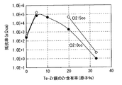
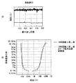
図10は、Te単体にZrをドープした膜のシート抵抗を測定し体積抵抗率を求めた結果を表したものである。図10から分かるように、Te−Zr膜の抵抗率は、Zr含有率が0%(純Te)から大きくなるにつれて上昇し、約7%程度で極大値となり、それ以上では低下する。このことから、中間層21AにZrを数%添加することにより中間層21Aの抵抗率を高くすることが可能であることが分かる。
FIG. 10 shows the results of measuring the volume resistivity by measuring the sheet resistance of a film obtained by doping Te alone with Zr. As can be seen from FIG. 10, the resistivity of the Te—Zr film increases as the Zr content increases from 0% (pure Te), reaches a maximum at about 7%, and decreases beyond that. From this, it can be seen that the resistivity of the
なお、Zrの外、Cu,Cr,Mn,TiまたはHf等の他の遷移金属も、Zrと同様に中間層21Aを高抵抗化する効果を有している。すなわち、中間層21Aは、Alとカルコゲン元素とを含み、更に、Zr,Cu,Cr,Mn,TiおよびHfからなる遷移金属の群のうち少なくとも1種を含んでいることが好ましい。
In addition to Zr, other transition metals such as Cu, Cr, Mn, Ti, or Hf also have the effect of increasing the resistance of the
このように本実施の形態では、中間層21Aが、Zr,Cu,Cr,Mn,TiおよびHfからなる遷移金属の群のうち少なくとも1種を含むことにより、中間層21Aの抵抗をイオン供給層21Bよりも高くするようにしたので、書き込み・消去動作時のイオン移動を促進して、メモリ動作を安定化し、書き込み・消去状態の抵抗分布を改善することが可能となる。
As described above, in the present embodiment, the
なお、変形例1,第2の実施の形態および変形例4は、本実施の形態にも適用可能である。すなわち、抵抗変化層22は、アルミニウム酸化物,遷移金属酸化物および遷移金属酸窒化物を混在した状態で含有する単層構造であってもよい。
Note that the first modification, the second embodiment, and the fourth modification are also applicable to this embodiment. That is, the
(第4の実施の形態)
図11は、本発明の第4の実施の形態に係る記憶素子1の断面構成を表したものである。この記憶素子1は、イオン源層21の中間層21Aおよびイオン供給層21Bのうち少なくとも一方に酸素(O)が添加されていることを除いては、上記第1ないし第3の実施の形態と同様の構成・作用および効果を有し、第1ないし第3の実施の形態と同様にして製造することができる。よって、対応する構成要素には同一の符号を付して説明する。
(Fourth embodiment)
FIG. 11 shows a cross-sectional configuration of the
イオン供給層21Bが酸素(O)を添加元素として含むことにより、イオン供給層21Bの抵抗率が大きくなる。そのため、書き込み動作時に、イオン供給層21B中の金属イオンにかかる分圧が大きくなり、金属イオンがより動きやすくなって、導電パスの形成がより安定する。よって、書き込み保持特性が向上する。なお、イオン供給層21Bの抵抗率は、成膜時の酸素(O2)流量によって制御可能であり、酸素(O2)導入量が大きくなるに従ってイオン供給層21Bの抵抗率も大きくなる。
When the
一方、中間層21Aが酸素(O)を添加元素として含むことにより、中間層21Aの抵抗率が高くなる。よって、消去動作時に中間層21Aにかかる電圧が大きくなり、金属イオンがイオン供給層21Bに戻りやすくなる。それと共に、導電パスの金属元素はイオン化し、イオン源層21に溶解、もしくはテルル(Te)等と結合して、より高抵抗な状態へと変化する反応が進みやすくなる。従って、消去特性が向上する。
On the other hand, when the
以上のことから、中間層21Aおよびイオン供給層21Bの両方が酸素(O)を添加元素として含むことにより、上述した書き込み保持特性および消去特性の両方が向上し、従来の書き込み/消去のトレードオフの関係から進歩し、多数ビットでの抵抗分離幅を更に改善することが可能となる。
From the above, when both the
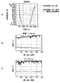
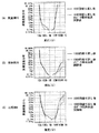
図12は、成膜時の酸素(O2)流量を0ccおよび5ccとした場合について、Te単体にZrをドープした膜のシート抵抗を測定し体積抵抗率を求めた結果を表したものである。なお、図12ではパワー,成膜時間等の成膜条件は固定した。図12から分かるように、Te−Zr膜の抵抗率は、成膜時の酸素(O2)流量を5ccとした場合のほうが、0ccとした場合よりも高くなっている。このことから、中間層21AにZrと酸素(O)とを両方添加することにより中間層21Aの抵抗率を高くし、好適な値とすることが可能であることが分かる。
FIG. 12 shows the result of measuring the volume resistivity by measuring the sheet resistance of a film doped with Zr on Te alone when the oxygen (O 2 ) flow rate during film formation is 0 cc and 5 cc. . In FIG. 12, film formation conditions such as power and film formation time are fixed. As can be seen from FIG. 12, the resistivity of the Te—Zr film is higher when the oxygen (O 2 ) flow rate during film formation is 5 cc than when it is 0 cc. From this, it is understood that the resistivity of the
なお、Zrの外、Cu,TiまたはHf等の他の遷移金属を酸素(O)と共に添加した場合にも、Zrと同様に中間層21Aを好適に高抵抗化する効果が得られる。すなわち、中間層21Aは、Alとカルコゲン元素とを含み、更に、酸素(O)と、Cu,Ti,ZrおよびHfからなる遷移金属の群のうち少なくとも1種とを添加元素として含むことが好ましい。
In addition to Zr, when other transition metals such as Cu, Ti, or Hf are added together with oxygen (O), the effect of appropriately increasing the resistance of the
また、図12では、Zr含有率が0%(純Te)の場合でも、成膜時の酸素(O2)流量を5ccとした場合のほうが、0ccとした場合よりも高抵抗となっている。従って、中間層21Aに遷移元素を添加せず、酸素(O)のみを添加することによっても中間層21Aの高抵抗化が可能となることが分かる。その場合には、中間層21Aは、Alとカルコゲン元素とを含むと共に、更に、酸素(O)を添加元素として含むことが好ましい。
Further, in FIG. 12, even when the Zr content is 0% (pure Te), the resistance when the oxygen (O 2 ) flow rate during film formation is 5 cc is higher than when the oxygen content is 0 cc. . Therefore, it can be seen that the resistance of the
以上のいずれの場合においても、中間層21Aは、イオン供給層21Bよりも高抵抗となっていることが好ましい。これにより、中間層21Aに電圧が印加されやすくなり、低電流でも動作しやすくなる。また、記憶素子1に電圧を印加した際に、より効率的にイオンが移動し、確実に書き込み・消去動作が可能となる。よって、動作不良が低減され、抵抗ばらつきが改善される。
In any of the above cases, the
このように本実施の形態では、イオン源層21の中間層21Aおよびイオン供給層21Bのうち少なくとも一方に酸素(O)を添加して抵抗率を高めるようにしたので、イオン供給層21Bへの酸素添加による書き込み保持特性の向上、または中間層21Aへの酸素添加による消去特性の向上が可能となり、多数ビットでの抵抗分離幅の改善が可能となる。
As described above, in this embodiment, oxygen (O) is added to at least one of the
なお、変形例1,第2の実施の形態および変形例4は、本実施の形態にも適用可能である。すなわち、抵抗変化層22は、アルミニウム酸化物,遷移金属酸化物および遷移金属酸窒化物を混在した状態で含有する単層構造であってもよい。
Note that the first modification, the second embodiment, and the fourth modification are also applicable to this embodiment. That is, the
(記憶装置)
上記記憶素子1を多数、例えば列状やマトリクス状に配列することにより、記憶装置(メモリ)を構成することができる。このとき、各記憶素子1に、必要に応じて、素子選択用のMOSトランジスタ、或いはダイオードを接続してメモリセルを構成し、更に、配線を介して、センスアンプ、アドレスデコーダ、書き込み・消去・読み出し回路等に接続すればよい。
(Storage device)
A memory device (memory) can be configured by arranging a large number of the
図13および図14は多数の記憶素子1をマトリクス状に配置した記憶装置(メモリセルアレイ2)の一例を表したものであり、図13は断面構成、図14は平面構成をそれぞれ表している。このメモリセルアレイ2では、各記憶素子1に対して、その下部電極10側に接続される配線と、その上部電極30側に接続される配線とを交差するよう設け、例えばこれら配線の交差点付近に各記憶素子1が配置されている。
13 and 14 show an example of a storage device (memory cell array 2) in which a large number of
各記憶素子1は、抵抗変化層22、イオン源層21および上部電極30の各層を共有している。すなわち、抵抗変化層22、イオン源層21および上部電極30それぞれは各記憶素子1に共通の層(同一層)により構成されている。上部電極30は、隣接セルに対して共通の電極となっている。
Each
一方、下部電極10は、メモリセル毎に個別に設けられることにより、隣接セル間で電気的に分離されており、各下部電極10に対応した位置に各メモリセルの記憶素子1が規定される。下部電極10は各々対応するセル選択用のMOSトランジスタTrに接続されており、各記憶素子1はこのMOSトランジスタTrの上方に設けられている。
On the other hand, the
MOSトランジスタTrは、半導体基板41内の素子分離層42により分離された領域に形成されたソース/ドレイン領域43とゲート電極44とにより構成されている。ゲート電極44の壁面にはサイドウォール絶縁層が形成されている。ゲート電極44は、記憶素子1の一方のアドレス配線であるワード線WLを兼ねている。MOSトランジスタTrのソース/ドレイン領域43の一方と、記憶素子1の下部電極10とが、プラグ層45、金属配線層46およびプラグ層47を介して電気的に接続されている。MOSトランジスタTrのソース/ドレイン領域43の他方は、プラグ層45を介して金属配線層46に接
続されている。金属配線層46は、記憶素子1の他方のアドレス配線であるビット線BL(図14参照)に接続されている。なお、図14においては、MOSトランジスタTrのアクティブ領域48を鎖線で示しており、コンタクト部51は記憶素子1の下部電極10、コンタクト部52はビット線BLにそれぞれ接続されている。
The MOS transistor Tr is composed of a source /
このメモリセルアレイ2では、ワード線WLによりMOSトランジスタTrのゲートをオン状態として、ビット線BLに電圧を印加すると、MOSトランジスタTrのソース/ドレインを介して、選択されたメモリセルの下部電極10に電圧が印加される。ここで、下部電極10に印加された電圧の極性が、上部電極30(共通電極)の電位に比して負電位である場合には、上述のように記憶素子1の抵抗値が低抵抗状態へと遷移する。これにより選択されたメモリセルに情報が書き込まれる。次に、下部電極10に、上部電極30(共通電極)の電位に比して正電位の電圧を印加すると、記憶素子1の抵抗値が再び高抵抗状態へと遷移する。これにより選択されたメモリセルに書き込まれた情報が消去される。書き込まれた情報の読み出しを行うには、例えば、MOSトランジスタTrによりメモリセルを選択し、そのセルに対して所定の電圧または電流を印加する。このときの記憶素子1の抵抗状態により異なる電流または電圧を、ビット線BLあるいは上部電極30(共通電極)の先に接続されたセンスアンプ等を介して検出する。なお、選択したメモリセルに対して印加する電圧または電流は、記憶素子1の抵抗値の状態が遷移する電圧等の閾値よりも小さくする。
In this
本実施の形態の記憶装置は、上述のように各種のメモリ装置に適用することができる。例えば、一度だけ書き込みが可能なPROM(Programmable Read Only Memory )、電気的に消去が可能なEEPROM(Erasable Programmable Read Only Memory)、或いは、高速に書き込み・消去・再生が可能な、いわゆるRAM等、いずれのメモリ形態でも適用することが可能である。 The storage device of this embodiment can be applied to various memory devices as described above. For example, PROM (Programmable Read Only Memory) that can be written only once, EEPROM (Erasable Programmable Read Only Memory) that can be electrically erased, or so-called RAM that can be written, erased and played back at high speed The present invention can also be applied to other memory forms.
以下、本発明の具体的な実施例について説明する。 Hereinafter, specific examples of the present invention will be described.
(実施例1)
上記第1の実施の形態と同様にして記憶素子1を備えたメモリセルアレイを作製した。まず、TiNよりなる下部電極10のプラグが形成してあるCMOS回路上に、スパッタリングによりTi膜を1nmの厚みで形成した。次いで、このTi膜を酸化プラズマで酸化してTiOxよりなる第1層22Aを形成した。
Example 1
A memory cell array including the
続いて、Teよりなる中間層21Aを4nmの厚みで形成し、引き続いてCuZrTeAlGe(Cu11at%−Zr11%−Te30%−Al40%−Ge8%)よりなるイオン供給層21Bを60nmの厚みで形成した。そののち、Wよりなる上部電極30を50nmの厚みで形成した。本実施例の工程を簡略的に示すと以下のようになる。
Subsequently, an
TiN/Ti(1nm)/プラズマ酸化/Te(4nm)/CuZrTeAlGe(60nm)/W(50nm) TiN / Ti (1nm) / Plasma oxidation / Te (4nm) / CuZrTeAlGe (60nm) / W (50nm)
下部電極10,記憶層20および上部電極30の積層膜を形成したのち、この積層膜のうち抵抗変化層22,イオン源層21および上部電極30を、メモリセルアレイの部分に残るようにパターニングした。また、上部電極30の表面に対してエッチングを行い、中間電位(Vdd/2)を与える外部回路に接続するための上部電極30のコンタクト部分を露出させた。
After forming a laminated film of the
積層膜をパターニングしたのち、Alよりなる配線層(図示せず)を200nmの厚みで形成し、この配線層と上部電極30のコンタクト部分とを接続した。そののち、積層膜に対して、真空熱処理炉で300℃、2時間の熱処理を行った。以上により、図1に示した記憶素子1を有するメモリセルアレイを作製した。
After patterning the laminated film, a wiring layer (not shown) made of Al was formed with a thickness of 200 nm, and the wiring layer and the contact portion of the
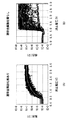
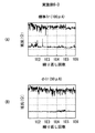
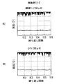
得られた実施例1のメモリセルアレイについて、繰り返し書き換え特性を調べた。その際、書き込みパルスとして電圧Vw3V,電流約100μA、パルス幅10ns、消去パルスとして電圧Ve2V、電流約100μA、パルス幅10nmで105以上繰り返した。その結果を図15(B)に示す。また、電流約50μAとして、同様に繰り返し書き換え特性を調べた。その結果を図15(C)に示す。 The obtained memory cell array of Example 1 was repeatedly checked for rewriting characteristics. At that time, 10 5 times or more were repeated with a voltage Vw of 3 V, a current of about 100 μA and a pulse width of 10 ns as a write pulse, a voltage Ve2V and a current of about 100 μA as an erase pulse and a pulse width of 10 nm. The result is shown in FIG. Further, the rewrite characteristics were repeatedly examined in the same manner at a current of about 50 μA. The result is shown in FIG.
図15(B)および図15(C)から分かるように、低抵抗状態と高抵抗状態の抵抗値が1桁以上異なる良好なメモリ動作を示した。 As can be seen from FIG. 15B and FIG. 15C, a good memory operation in which the resistance values in the low resistance state and the high resistance state differed by one digit or more was shown.
次に、4kbitのメモリセルアレイで1000回繰り返し後の、累積度数分布と、130℃2時間のデータ保持加速試験後の累積度数分布とを調べた。その結果を図15(A)に示す。 Next, the cumulative frequency distribution after 1000 repetitions in a 4 kbit memory cell array and the cumulative frequency distribution after a data retention acceleration test at 130 ° C. for 2 hours were examined. The result is shown in FIG.
図15(A)から分かるように、書き込み状態(低抵抗)と消去状態(高抵抗)とが分離していると共に良好なばらつき特性を示しており、データ保持加速試験後でも抵抗分離が得られていた。 As can be seen from FIG. 15A, the writing state (low resistance) and the erasing state (high resistance) are separated and exhibit excellent variation characteristics, and resistance separation is obtained even after the data retention acceleration test. It was.
(実施例2)
TiNよりなる下部電極10のプラグが形成してあるCMOS回路上で、下部電極10上に形成されている自然酸化皮膜を逆スパッタで十分に除去した。そののち、下部電極10を直接プラズマ酸化することによりTiOxよりなる第1層22Aを形成した。このことを除いては、実施例1と同様にして記録素子1を有するメモリセルアレイを作製した。実施例2の工程を簡略的に示すと以下のようになる。
(Example 2)
On the CMOS circuit where the plug of the
TiN/プラズマ酸化/Te(4nm)/CuZrTeAlGe(60nm)/W(50nm) TiN / plasma oxidation / Te (4nm) / CuZrTeAlGe (60nm) / W (50nm)
(実施例3)
Wよりなる下部電極10のプラグが形成してあるCMOS回路上で、下部電極10上に形成されている自然酸化皮膜を逆スパッタで十分に除去した。そののち、下部電極10を直接プラズマ酸化することにより酸化タングステン(WOx)よりなる第1層22Aを形成した。このことを除いては、実施例1と同様にして記録素子1を有するメモリセルアレイを作製した。実施例3の工程を簡略的に示すと以下のようになる。
(Example 3)
On the CMOS circuit in which the plug of the
W/プラズマ酸化/Te(4nm)/CuZrTeAlGe(60nm)/W(50nm) W / Plasma oxidation / Te (4nm) / CuZrTeAlGe (60nm) / W (50nm)
(比較例1)
TiNよりなる下部電極のプラグが形成してあるCMOS回路上に、スパッタリングによりガドリニウム(Gd)膜を1nmの厚みで形成した。このGd膜を酸化プラズマで酸化することにより、酸化ガドリニウム(GdOx)膜を形成した。そののち、CuZrTeAlGe(Cu11at%−Zr11%−Te30%−Al40%−Ge8%)よりなるイオン源層を60nmの厚みで形成し、Wよりなる上部電極を50nmの厚みで形成した。このことを除いては、実施例1と同様にして記録素子を有するメモリセルアレイを作製した。比較例1の工程を簡略的に示すと以下のようになる。
(Comparative Example 1)
A gadolinium (Gd) film having a thickness of 1 nm was formed by sputtering on a CMOS circuit having a lower electrode plug made of TiN. This Gd film was oxidized with oxidation plasma to form a gadolinium oxide (GdOx) film. After that, an ion source layer made of CuZrTeAlGe (Cu11at% -Zr11% -Te30% -Al40% -Ge8%) was formed with a thickness of 60 nm, and an upper electrode made of W was formed with a thickness of 50 nm. Except for this, a memory cell array having recording elements was fabricated in the same manner as in Example 1. The process of Comparative Example 1 is simply shown as follows.
TiN/Gd(1nm)/プラズマ酸化/CuZrTeAlGe(60nm)/W(50nm) TiN / Gd (1nm) / Plasma oxidation / CuZrTeAlGe (60nm) / W (50nm)
(比較例2)
TiNよりなる下部電極のプラグが形成してあるCMOS回路上に、スパッタリングによりGd膜を1nmの厚みで形成した。このGd膜を酸化プラズマで酸化することにより、GdOx膜を形成した。続いて、Teよりなる中間層を4nmの厚みで成膜し、CuZrTeAlGe(Cu11at%−Zr11%−Te30%−Al40%−Ge8%)よりなるイオン供給層を60nmの厚みで形成した。そののち、Wよりなる上部電極を50nmの厚みで形成した。このことを除いては、実施例1と同様にして記録素子を有するメモリセルアレイを作製した。比較例2の工程を簡略的に示すと以下のようになる。
(Comparative Example 2)
A Gd film having a thickness of 1 nm was formed by sputtering on a CMOS circuit on which a plug of a lower electrode made of TiN was formed. The GdOx film was formed by oxidizing the Gd film with oxidation plasma. Subsequently, an intermediate layer made of Te was formed with a thickness of 4 nm, and an ion supply layer made of CuZrTeAlGe (Cu11at% -Zr11% -Te30% -Al40% -Ge8%) was formed with a thickness of 60 nm. After that, an upper electrode made of W was formed with a thickness of 50 nm. Except for this, a memory cell array having recording elements was fabricated in the same manner as in Example 1. The process of Comparative Example 2 is simply shown as follows.
TiN/Gd(1nm)/プラズマ酸化/Te(4nm)/CuZrTeAlGe(60nm)/W(50nm) TiN / Gd (1nm) / Plasma oxidation / Te (4nm) / CuZrTeAlGe (60nm) / W (50nm)
(比較例3)
TiNよりなる下部電極のプラグが形成してあるCMOS回路上に、スパッタリングによりTeよりなる中間層を4nmの厚みで形成した。続いて、CuZrTeAlGe(Cu11at%−Zr11%−Te30%−Al40%−Ge8%)よりなるイオン供給層を60nmの厚みで形成し、Wよりなる上部電極を50nmの厚みで形成した。このことを除いては、実施例1と同様にして記録素子1を有するメモリセルアレイを作製した。比較例3の工程を簡略的に示すと以下のようになる。
(Comparative Example 3)
An intermediate layer made of Te with a thickness of 4 nm was formed on the CMOS circuit on which the plug of the lower electrode made of TiN was formed by sputtering. Subsequently, an ion supply layer made of CuZrTeAlGe (Cu11at% -Zr11% -Te30% -Al40% -Ge8%) was formed with a thickness of 60 nm, and an upper electrode made of W was formed with a thickness of 50 nm. Except for this, a memory cell array having the
TiN/Te(4nm)/ CuZrTeAlGe(60nm)/W(50nm) TiN / Te (4nm) / CuZrTeAlGe (60nm) / W (50nm)
得られた実施例2,3および比較例1,2,3のメモリセルアレイについても、実施例1と同様にして、1000回繰り返し後の4kbitの累積度数分布、および/または100μAと50μAとの繰り返し特性を調べた。実施例2の累積度数分布を図16(A)、実施例2の繰り返し特性を図16(B)および図16(C)に示す。実施例3の繰り返し特性を図17(A)および図17(B)に示す。比較例1の累積度数分布を図18(A)、比較例1の繰り返し特性を図18(B)および図18(C)に示す。比較例2の繰り返し特性を図19(A)および図19(B)に示す。比較例3の累積度数分布を図20(A)、比較例3の繰り返し特性を図20(B)および図20(C)に示す。 For the obtained memory cell arrays of Examples 2 and 3 and Comparative Examples 1, 2 and 3, as in Example 1, the cumulative frequency distribution of 4 kbits after 1000 repetitions and / or repetition of 100 μA and 50 μA The characteristics were investigated. The cumulative frequency distribution of Example 2 is shown in FIG. 16 (A), and the repetition characteristics of Example 2 are shown in FIGS. 16 (B) and 16 (C). The repetition characteristics of Example 3 are shown in FIGS. 17 (A) and 17 (B). The cumulative frequency distribution of Comparative Example 1 is shown in FIG. 18 (A), and the repetition characteristics of Comparative Example 1 are shown in FIGS. 18 (B) and 18 (C). The repetition characteristics of Comparative Example 2 are shown in FIGS. 19 (A) and 19 (B). The cumulative frequency distribution of Comparative Example 3 is shown in FIG. 20 (A), and the repetition characteristics of Comparative Example 3 are shown in FIGS. 20 (B) and 20 (C).
(実施例1,2および比較例3:遷移金属酸化物よりなる第1層の有無)
図15(A)〜(C),図16(A)〜(C)および図20(A)〜(C)から分かるように、下部電極10上にTiOxよりなる第1層22Aを形成した実施例1,2ではいずれも良好な抵抗分離および繰り返し特性が得られた。これに対して、遷移金属酸化物よりなる第1層を設けず、下部電極の上に直接中間層およびイオン供給層を形成した比較例3では、高抵抗状態および低抵抗状態の分離が得られておらず、繰り返し特性に劣っていた。
(Examples 1 and 2 and Comparative Example 3: Presence / absence of first layer made of transition metal oxide)
15A to 15C, FIGS. 16A to 16C, and FIGS. 20A to 20C, the
この原因は必ずしも明らかではないものの、原因を推定する測定の例として書き込み動作を行った低抵抗状態の60個の素子に、消去方向に0〜3Vまで電圧を加えていったときの抵抗変化を図21(A)および図21(B)に示す。図21(B)に示したように、遷移金属酸化物よりなる第1層を形成していない場合は、消去電圧によって低抵抗化する素子が多く存在する。これに対して、図21(A)に示したように、遷移金属酸化物よりなる第1層を形成している素子では、測定の範囲内の消去電圧では低抵抗化していない。これは、下部電極の上に遷移金属酸化物よりなる第1層が存在することにより、消去電圧がかかった際にAl酸化膜が形成されるなどの高抵抗化する以外の不要な変化を抑制しているためと考えられ、おそらくは本実施例で電解質のアニオンであるTeと下部電極との反応を抑制しているためと考えられる。 Although this cause is not necessarily clear, as an example of measurement for estimating the cause, the resistance change when a voltage of 0 to 3 V is applied in the erase direction to 60 elements in a low resistance state in which a write operation was performed. It is shown in FIG. 21 (A) and FIG. 21 (B). As shown in FIG. 21B, in the case where the first layer made of the transition metal oxide is not formed, there are many elements whose resistance is lowered by the erase voltage. On the other hand, as shown in FIG. 21A, in the element in which the first layer made of the transition metal oxide is formed, the resistance is not lowered at the erase voltage within the measurement range. This suppresses unnecessary changes other than high resistance such as the formation of an Al oxide film when an erase voltage is applied due to the presence of the first layer of transition metal oxide on the lower electrode. This is probably because the reaction between Te, which is an anion of the electrolyte, and the lower electrode is suppressed in this example.
更に、実施例2の記憶素子1について、電子顕微鏡(TEM;Transmission Electron Microscope)による構造解析およびEDX測定を行った。TEM−EDX像を図22に示すと共に、断面のEDXラインプロファイル結果を図23および図24に示す。EDX測定では、断面サンプル上で約1nm径に収光した電子線を1nm間隔でラインスキャンしがなら、各ポイントにおけるEDXスペクトルを取得した。EDXラインプロファイル結果は、Te−Lα1ピーク,Cu−Kα1ピーク,O−Kα1ピーク,Al−Kα1ピーク,Zr−Kα1ピーク,Ti−Kα1ピークの積分強度をプロットした結果である。各ピークの積分強度は、バックグラウンドのノイズ成分を含んだ値である。
Further, the
図23および図24から分かるように、実施例2では、TiOxよりなる第1層22AとTeを含む中間層21Aとの界面に、Alおよび酸素(O)のピークが観察されており、酸化アルミニウム(Al−O)よりなる第2層22Bが形成されていることを確認できた。第2層22Bの存在は、図22のTEM像でも認められた。また、ここでは示していないが、下部電極上に遷移金属酸化物よりなる第1層を形成していない比較例3のTEM像でも、下部電極上にAl酸化層が形成されることが分かっている。しかし、実施例2および比較例3の繰り返し特性は大きく異なり、実施例2では100万回以上の書き換え繰り返しを行っても特性劣化が少なく更に書き換えが可能であるが、遷移金属酸化物よりなる第1層を形成していない比較例3では10回繰り返し後には特性が大きく劣化している。
As can be seen from FIGS. 23 and 24, in Example 2, peaks of Al and oxygen (O) are observed at the interface between the
すなわち、抵抗変化層22が、下部電極10の側から順に、遷移金属酸化物よりなる第1層22Aと、アルミニウム酸化物を主成分とする第2層22Bとを積層した構成を有しているようにすれば、良好な抵抗分離および繰り返し特性を得ることができることが分かった。
That is, the
(実施例3および比較例2:遷移金属酸化物よりなる第1層の他の材料)
図17(A)および図17(B)から分かるように、WOxよりなる第1層22Aを設けた実施例3では、実施例1,2と同様に良好な抵抗分離および繰り返し特性が得られた。
(Example 3 and Comparative Example 2: Other materials of first layer made of transition metal oxide)
As can be seen from FIGS. 17 (A) and 17 (B), in Example 3 provided with the
これに対して、図19(A)および図19(B)から分かるように、抵抗変化層としてGdOx膜を形成した比較例2では、初期抵抗値が高くなりすぎて書き込み(低抵抗化)動作しがたくなるため、繰り返しが困難となった。 On the other hand, as can be seen from FIGS. 19A and 19B, in Comparative Example 2 in which the GdOx film is formed as the variable resistance layer, the initial resistance value becomes too high, and the write (low resistance) operation is performed. It became difficult to repeat, making it difficult to repeat.
すなわち、第1層22Aが、TiOxのほか、WOxにより構成されている場合にも、良好な抵抗分離および繰り返し特性を得ることができることが分かった。
That is, it was found that good resistance separation and repeatability can be obtained even when the
(実施例1〜3および比較例1:中間層の有無による低電流での繰り返し特性の違い)
図18(B)および図18(C)から分かるように、下部電極上にGdOx)よりなる抵抗変化層を形成し、中間層を設けていない比較例1では、100μAの繰り返し後の抵抗分離は比較的良好であったものの、50μAの繰り返し特性は、中間層21Aを設けた実施例1〜3に比べて劣っていた。
(Examples 1 to 3 and Comparative Example 1: Difference in repetitive characteristics at low current depending on the presence or absence of an intermediate layer)
As can be seen from FIG. 18B and FIG. 18C, in Comparative Example 1 in which the resistance change layer made of GdOx) is formed on the lower electrode and the intermediate layer is not provided, the resistance separation after 100 μA repetition is Although it was comparatively good, the repeatability of 50 μA was inferior to Examples 1 to 3 provided with the
すなわち、イオン源層21を中間層21Aとイオン供給層21Bとの2層構造とすれば、より低電流での繰り返し特性が向上することが分かった。
That is, it has been found that if the
(実施例2:中間層およびイオン供給層のアルミニウム濃度分布)
上述した実施例2では、遷移金属酸化物よりなる第1層22Aを形成したのちTeよりなる中間層21AおよびCuZrTeAlGeよりなるイオン供給層21Bを順に形成した。しかしながら、実際には成膜後に、図22のTEM像、並びに図23および図24のEDXラインプロファイル結果から分かるように、イオン供給層21Bから中間層21AにAlが拡散し、中間層21AにもAlが存在している状態となっていた。ただし、TEM像からは中間層21Aではイオン供給層21Bよりもカルコゲン元素含有量に対するAl含有量の比(Al濃度)が低いことが分かり、このことが本実施例の効果を発揮させているものと考えられる。つまりは、中間層21AにTeがアニオンとして豊富に存在し、書き込み・消去、特に消去動作時のAlイオンの移動を妨げないことが必要である。また、中間層21A中のAlは、イオン供給層21Bとの濃度勾配による拡散によってもたらされると考えられるので、例えばAl2Te3の化学量論組成よりも少なくなると考えられ、中間層21Aに存在しているAlのほとんどはイオン状態で存在していると考えられ、印加した電位が効果的にイオン移動の駆動に用いられることがこのような特性向上に結びついていると考えられる。
(Example 2: Aluminum concentration distribution in intermediate layer and ion supply layer)
In Example 2 described above, after forming the
すなわち、中間層21AにおけるAl濃度がイオン供給層21BにおけるAl濃度よりも小さくなるようにすれば、低電流での繰り返し特性を向上させることができることが分かった。
That is, it has been found that if the Al concentration in the
(実施例2および比較例1:中間層の有無によるデータ保持特性の違い)
図16(A)および図18(A)から分かるように、中間層を設けない比較例1では、繰り返し後の保持加速試験後において低抵抗状態のビットが高抵抗化し、分布が変化している様子が見られた。これに対して、中間層を有する実施例2では、低抵抗状態の分布に変化は見られず良好なデータ保持特性を示した。この原因は必ずしも明らかではないが、実施例2ではイオン供給層21BよりもAl濃度の低い中間層21Aが存在することで、書き込み動作時の還元反応によって、Alイオンが還元されてAlメタルが生成し、書き込み電圧バイアスを取り去ったときに再びAl酸化物となって素子抵抗を上昇させるのでなく、Alを溶解する余力のある中間層21AにメタルAlが溶解することによって抵抗上昇が生じないためと考えられる。
(Example 2 and Comparative Example 1: Difference in data retention characteristics depending on presence / absence of intermediate layer)
As can be seen from FIGS. 16A and 18A, in Comparative Example 1 in which the intermediate layer is not provided, the bit in the low resistance state becomes high resistance after the repeated holding acceleration test, and the distribution changes. The situation was seen. On the other hand, in Example 2 having an intermediate layer, no change was observed in the distribution of the low resistance state, and good data retention characteristics were shown. Although this cause is not necessarily clear, in Example 2, the presence of the
すなわち、イオン源層21を中間層21Aとイオン供給層21Bとの2層構造とすれば、データ保持特性を向上することができることが分かった。
That is, it has been found that if the
(実施例4−1)
第1層22Aを、Ta膜をプラズマ酸化することにより形成したことを除いては、実施例1と同様にしてメモリセルアレイを作製した。得られたメモリセルアレイについて繰り返し書き換え特性および抵抗分離を調べたところ、図25(A)および図25(B)に示したように、実施例1と同等の結果が得られた。
(Example 4-1)
A memory cell array was fabricated in the same manner as in Example 1 except that the
(実施例4−2)
第1層22Aを、Zr膜をプラズマ酸化することにより形成したことを除いては、実施例1と同様にしてメモリセルアレイを作製した。得られたメモリセルアレイについて繰り返し書き換え特性および抵抗分離を調べたところ、図26(A)および図26(B)に示したように、実施例1と同等の結果が得られた。
(Example 4-2)
A memory cell array was fabricated in the same manner as in Example 1 except that the
(実施例5−1)
中間層21AをGeS、イオン供給層21BをCuZrTeAlGeにより構成したことを除いては、実施例1と同様にしてメモリセルアレイを作製した。得られたメモリセルアレイについて、繰り返し書き換え特性および抵抗分離を調べたところ、図27(A)および図27(B)に示したように、実施例1と同等の結果が得られた。
(Example 5-1)
A memory cell array was fabricated in the same manner as in Example 1 except that the
(実施例5−2)
中間層21AをTe、イオン供給層21BをCuTiTeAlにより構成したことを除いては、実施例1と同様にしてメモリセルアレイを作製した。得られたメモリセルアレイについて、繰り返し書き換え特性および抵抗分離を調べたところ、実施例1と同等の結果が得られた。
(Example 5-2)
A memory cell array was fabricated in the same manner as in Example 1 except that the
(実施例6−1)
中間層21AをTe(厚み5nm)、イオン供給層21BをAg7Zr14Te36Al43(厚み45nm)、上部電極30をZr(厚み50nm)により構成したことを除いては、実施例2と同様にしてメモリセルアレイを作製した。得られたメモリセルアレイについて、繰り返し書き換え特性および抵抗分離を調べたところ、図28(A)および図28(B)に示したように、実施例2と同等の結果が得られた。
(Example 6-1)
A memory cell array is fabricated in the same manner as in Example 2 except that the
(実施例6−2)
中間層21AをTe(厚み5nm)、イオン供給層21BをNi13Zr13Te33Al40(厚み45nm)、上部電極30をZr(厚み50nm)により構成したことを除いては、実施例2と同様にしてメモリセルアレイを作製した。得られたメモリセルアレイについて、繰り返し書き換え特性および抵抗分離を調べたところ、図29(A)および図29(B)に示したように、実施例2と同等の結果が得られた。
(Example 6-2)
A memory cell array is fabricated in the same manner as in Example 2 except that the
(実施例6−3)
中間層21AをTe(厚み5nm)、イオン供給層21BをCo7Zr14Te36Al43(厚み45nm)、上部電極30をZr(厚み50nm)により構成したことを除いては、実施例2と同様にしてメモリセルアレイを作製した。得られたメモリセルアレイについて、繰り返し書き換え特性および抵抗分離を調べたところ、図30(A)および図30(B)に示したように、実施例2と同等の結果が得られた。
(Example 6-3)
A memory cell array is manufactured in the same manner as in Example 2 except that the
(実施例6−4)
中間層21AをTe(厚み5nm)、イオン供給層21BをMn13Zr13Te33Al40(厚み45nm)、上部電極30をZr(厚み50nm)により構成したことを除いては、実施例2と同様にしてメモリセルアレイを作製した。得られたメモリセルアレイについて、繰り返し書き換え特性および抵抗分離を調べたところ、図31(A)および図31(B)に示したように、実施例2と同等の結果が得られた。
(Example 6-4)
A memory cell array is fabricated in the same manner as in Example 2 except that the
(実施例6−5)
中間層21AをTe(厚み5nm)、イオン供給層21BをFe10Zr16Te39Al35(厚み45nm)、上部電極30をZr(厚み50nm)により構成したことを除いては、実施例2と同様にしてメモリセルアレイを作製した。得られたメモリセルアレイについて、繰り返し書き換え特性および抵抗分離を調べたところ、図32(A)および図32(B)に示したように、実施例2と同等の結果が得られた。
(Example 6-5)
A memory cell array was fabricated in the same manner as in Example 2 except that the
(実施例7−1)
イオン供給層21BをCu10Hf14Te37Al38により構成したことを除いては、実施例2と同様にしてメモリセルアレイを作製した。得られたメモリセルアレイについて、累積度数分布,繰り返し書き換え特性および抵抗分離を調べたところ、図33(A)ないし図33(C)に示したように、実施例2と同等の結果が得られた。
(Example 7-1)
A memory cell array was fabricated in the same manner as in Example 2 except that the
(実施例7−2)
イオン供給層21BをCu10Ti14Te37Al38により構成したことを除いては、実施例2と同様にしてメモリセルアレイを作製した。得られたメモリセルアレイについて、累積度数分布,繰り返し書き換え特性および抵抗分離を調べたところ、図34(A)ないし図34(C)に示したように、実施例2と同等の結果が得られた。
(Example 7-2)
A memory cell array was fabricated in the same manner as in Example 2 except that the
(実施例7−3)
中間層21AをAl1Te9(厚み3.2nm)、イオン供給層21BをCu12.5Hf7.5Te35.4Al38Ge6.6(厚み60nm)、上部電極30をタングステン(W)(厚み30nm)により構成したことを除いては、実施例2と同様にしてメモリセルアレイを作製した。得られたメモリセルアレイについて、累積度数分布,繰り返し書き換え特性および抵抗分離を調べたところ、図35(A)ないし図35(C)に示したように、実施例2と同等の結果が得られた。
(Example 7-3)
The
(実施例8−1〜8−4)
実施例2と同様にして4kbitのメモリセルアレイを作製した。その際、窒化チタン(TiN)よりなる下部電極10の表面を直接プラズマ酸化することにより酸化チタン(TiOx)よりなる第1層22Aを形成した。得られた四つのサンプル(実施例8−1〜8−4)について、第1層22Aの厚みおよび密度を、X線反射率法を用いて調べた。その結果を表1に示す。
(Examples 8-1 to 8-4)
A 4 kbit memory cell array was fabricated in the same manner as in Example 2. At that time, the surface of the

得られた実施例8−1〜8−4のメモリセルアレイについて、1000回の書き込み・消去動作を繰り返し、続いて温度加速試験を行ったのちに、累積度数分布を調べた。その結果を図36(A),図36(B),図37(A)および図37(B)に示す。 With respect to the obtained memory cell arrays of Examples 8-1 to 8-4, 1000 times of programming / erasing operations were repeated, followed by a temperature acceleration test, and then the cumulative frequency distribution was examined. The results are shown in FIGS. 36 (A), 36 (B), 37 (A), and 37 (B).
表1および図36(A)ないし図37(B)から分かるように、実施例8−1〜8−4はいずれも第1層22Aの厚みが1nm以上であり、書き込み(低抵抗)状態と消去(高抵抗)状態が分離されていた。すなわち、第1層22Aの厚みを1nm以上とすれば、良好な抵抗分離特性を得られることが確認された。
As can be seen from Table 1 and FIGS. 36A to 37B, in each of Examples 8-1 to 8-4, the thickness of the
(実施例9−1,9−2)
実施例1と同様にして4kbitのメモリセルアレイを作製した。その際、TiNよりなる下部電極10の上面に、遷移金属材料膜としてZr膜を形成し、このZr膜を酸化することにより、ZrOx層22A1を形成した。その際、結果としてTiOx層22A2も形成され、図2における第1層22Aが形成された。また、本実施例ではZrを用いてZrOx層22A1を形成したが、ZrNを酸化することにより、ZrOx層22A1を形成してもよい。(図2参照。)。
(Examples 9-1 and 9-2)
A 4 kbit memory cell array was fabricated in the same manner as in Example 1. At that time, a Zr film as a transition metal material film was formed on the upper surface of the
得られた二つのサンプル(実施例9−1,9−2)について、第1層22Aの厚みおよび密度を調べたところ、実施例9−1では、TiOx層22A2の厚みは1.49nm、密度は3.86g/cm3、ZrOx層22A1の厚みは1.48nm、密度は5.23g/cm3であった。実施例9−2では、TiOx層22A2の厚みは2.39nm、密度は3.70g/cm3、ZrOx層22A1の厚みは1.07nm、密度は5.17g/cm3であった。
When the thickness and density of the
更に、実施例9−1,9−2のメモリセルアレイについて、1000回の書き込み・消去動作を繰り返し、続いて温度加速試験を行ったのちに、累積度数分布を調べた。その結果を図38(A)および図38(B)に示す。 Further, with respect to the memory cell arrays of Examples 9-1 and 9-2, 1000 times of programming / erasing operations were repeated, followed by a temperature acceleration test, and then the cumulative frequency distribution was examined. The results are shown in FIGS. 38 (A) and 38 (B).
図38(A)および図38(B)から分かるように、実施例9−1,9−2はいずれも第1層22Aの厚みが1nm以上であり、書き込み(低抵抗)状態と消去(高抵抗)状態が分離されていた。すなわち、第1層22Aの厚みを1nm以上とすれば、良好な抵抗分離特性を得られることが確認された。
38A and 38B, in each of Examples 9-1 and 9-2, the thickness of the
(実施例10:第1層22Aを酸窒化物により構成した例)
上記第2の実施の形態と同様にして記憶素子1を備えたメモリセルアレイを作製した。まず、TiNよりなる下部電極10のプラグが形成してあるCMOS回路上に、リアクティブスパッタによりZrN膜を0.5nmの厚みで形成した。成膜条件としては、Zrターゲットに印加する電圧は3.5kW、チャンバー内に流すアルゴン(Ar),窒素(N2)の流量はそれぞれ25sccm,300sccmとし、全体の圧力は2.1E-3(Torr)とした。このときのAr雰囲気の分圧は2.0E-4(Torr)、窒素雰囲気の分圧は1.9E-3(Torr)と見積もっている。次いで、このZrN膜を酸化プラズマで酸化してZrONよりなる第1層22Aを形成した。
(Example 10: Example in which the
A memory cell array provided with the
続いて、Teよりなる中間層21Aを5nmの厚みで形成し、引き続いてCuZrTeAlGe(Cu11at%−Zr11%−Te30%−Al40%−Ge8%)よりなるイオン供給層21Bを60nmの厚みで形成した。そののち、Wよりなる上部電極30を50nmの厚みで形成した。本実施例の工程を簡略的に示すと以下のようになる。
Subsequently, an
TiN/ZrN(0.5nm)/プラズマ酸化/Te(5nm)/CuZrTeAlGe(60nm)/W(50nm) TiN / ZrN (0.5nm) / Plasma oxidation / Te (5nm) / CuZrTeAlGe (60nm) / W (50nm)
下部電極10,記憶層20および上部電極30の積層膜を形成したのち、実施例1と同様にして積層膜のパターニングおよび熱処理を行った。以上により、図6に示した記憶素子1を有するメモリセルアレイを作製した。
After forming the laminated film of the
得られた実施例10のメモリセルアレイについて、累積度数分布,繰り返し書き換え特性および抵抗分離を調べたところ、図39(A)ないし図39(C)に示したように、累積度数分布,繰り返し特性および抵抗分離のいずれも、上記実施の形態の遷移金属酸化物または遷移金属酸窒化物を用いていない比較例1に比べて良好な特性が得られた。 The obtained memory cell array of Example 10 was examined for cumulative frequency distribution, repeated rewrite characteristics, and resistance isolation. As shown in FIGS. 39A to 39C, the cumulative frequency distribution, repeated characteristics, and In any of the resistance separations, better characteristics were obtained than in Comparative Example 1 in which the transition metal oxide or transition metal oxynitride of the above embodiment was not used.
すなわち、抵抗変化層22が、下部電極10の側から順に、遷移金属酸窒化物よりなる第1層22Aと、アルミニウム酸化物を主成分とする第2層22Bとを積層した構成を有しているようにすれば、良好な抵抗分離および繰り返し特性を得ることができることが分かった。
That is, the
(実施例11:中間層21Aに遷移金属を添加した例)
上記第3の実施の形態と同様にして記憶素子1を備えたメモリセルアレイを作製した。まず、TiNよりなる下部電極10のプラグが形成してあるCMOS回路上に、実施例10と同様にしてリアクティブスパッタによりZrN膜を0.5nmの厚みで形成した。次いで、このZrN膜を酸化プラズマで酸化してZrONよりなる第1層22Aを形成した。
(Example 11: Example of adding transition metal to
A memory cell array provided with the
続いて、Te95Zr5よりなる中間層21Aを5nmの厚みで形成し、引き続いてCuZrTeAlGe(Cu11at%−Zr11%−Te30%−Al40%−Ge8%)よりなるイオン供給層21Bを60nmの厚みで形成した。そののち、タングステン(W)よりなる上部電極30を50nmの厚みで形成した。本実施例の工程を簡略的に示すと以下のようになる。
Subsequently, an
TiN/ZrN(0.5nm)/プラズマ酸化/Te95Zr5(5nm)/CuZrTeAlGe(60nm)/W(50nm) TiN / ZrN (0.5nm) / Plasma oxidation / Te95Zr5 (5nm) / CuZrTeAlGe (60nm) / W (50nm)
下部電極10,記憶層20および上部電極30の積層膜を形成したのち、実施例1と同様にして積層膜のパターニングおよび熱処理を行った。以上により、図9に示した記憶素子1を有するメモリセルアレイを作製した。
After forming the laminated film of the
得られた実施例11のメモリセルアレイについて、累積度数分布,繰り返し書き換え特性および抵抗分離を調べたところ、図40(A)ないし図40(C)に示したように、累積度数分布,繰り返し特性および抵抗分離のいずれも、上記実施の形態の遷移金属酸化物または遷移金属酸窒化物を用いていない比較例1に比べて良好な特性が得られた。 The obtained memory cell array of Example 11 was examined for cumulative frequency distribution, repeated rewrite characteristics, and resistance separation. As shown in FIGS. 40A to 40C, the cumulative frequency distribution, repeated characteristics, and In any of the resistance separations, better characteristics were obtained than in Comparative Example 1 in which the transition metal oxide or transition metal oxynitride of the above embodiment was not used.
また、実施例10,11のメモリセルアレイについて、書き込み動作を行った低抵抗状態の60個の素子に、消去方向に0〜3Vまで電圧を加えていったときの抵抗変化を調べた。その結果を図41(A)および図41(B)に示す。図41(A)および図41(B)から分かるように、測定の範囲内の消去電圧では低抵抗化しておらず、実施例1と同等以上の消去特性をもっていることが確認された。 In addition, for the memory cell arrays of Examples 10 and 11, changes in resistance were examined when a voltage of 0 to 3 V was applied in the erase direction to 60 elements in the low resistance state in which the write operation was performed. The results are shown in FIGS. 41 (A) and 41 (B). As can be seen from FIGS. 41A and 41B, it was confirmed that the erase voltage within the measurement range was not reduced in resistance and had an erase characteristic equal to or higher than that of Example 1.
すなわち、抵抗変化層22が、下部電極10の側から順に、遷移金属酸窒化物よりなる第1層22Aと、アルミニウム酸化物を主成分とする第2層22Bとを積層した構成を有すると共に、イオン源層21を中間層21Aとイオン供給層21Bとの2層構造とし、中間層21Aに遷移金属としてZrを添加するようにすれば、良好な抵抗分離および繰り返し特性を得ることができることが分かった。
That is, the
(実施例12:中間層21Aに遷移金属を添加した例)
下部電極10にWNを用いた以外は,実施例11と同様にしてメモリセルアレイを作製した。本実施例の工程を簡略的に示すと以下のようになる。
(Example 12: Example of adding transition metal to
A memory cell array was fabricated in the same manner as in Example 11 except that WN was used for the
WN/ZrN(0.5nm)/プラズマ酸化/Te95Zr5(5nm)/CuZrTeAlGe(60nm)/W(50nm) WN / ZrN (0.5nm) / Plasma oxidation / Te95Zr5 (5nm) / CuZrTeAlGe (60nm) / W (50nm)
得られた実施例12のメモリセルアレイについて、累積度数分布,繰り返し書き換え特性および抵抗分離を調べたところ、図42(A)ないし図42(C)に示したように、累積度数分布,繰り返し特性および抵抗分離のいずれも、上記実施の形態の遷移金属酸化物または遷移金属酸窒化物を用いていない比較例1に比べて良好な特性が得られた。 The obtained memory cell array of Example 12 was examined for cumulative frequency distribution, repetitive rewriting characteristics, and resistance separation. As shown in FIGS. 42A to 42C, the cumulative frequency distribution, repetitive characteristics, and In any of the resistance separations, better characteristics were obtained than in Comparative Example 1 in which the transition metal oxide or transition metal oxynitride of the above embodiment was not used.
すなわち、抵抗変化層22が、下部電極10の側から順に、遷移金属酸窒化物よりなる第1層22Aと、アルミニウム酸化物を主成分とする第2層22Bとを積層した構成を有すると共に、イオン源層21を中間層21Aとイオン供給層21Bとの2層構造とし、中間層21Aに遷移金属としてZrを添加するようにすれば、下部電極10がTiNのほか、WNにより構成されている場合にも、良好な抵抗分離および繰り返し特性を得ることができることが分かった。
That is, the
(実施例13−1〜13−3:第1層の酸窒化物の他の材料)
実施例10と同様にして記憶素子1を備えたメモリセルアレイを作製した。その際、TiNよりなる下部電極10のプラグが形成してあるCMOS回路上に、実施例13−1ではTiN膜、実施例13−2では窒化タンタル(TaN)膜、実施例13−3では窒化ハフニウム(HfN)膜をそれぞれ形成した。それぞれの膜を酸化プラズマで酸化して、実施例13−1ではTiON、実施例13−2ではタンタルの酸窒化物(TaON)、実施例13−3ではハフニウムの酸窒化物(HfON)よりなる第1層22Aを形成した。
(Examples 13-1 to 13-3: Other materials of first layer oxynitride)
A memory cell array including the
得られた実施例13−1〜13−3のメモリセルアレイについて、繰り返し書き換え特性および抵抗分離を調べたところ、図43ないし図45に示したように、上記実施の形態の遷移金属酸化物または遷移金属酸窒化物を用いていない比較例1に比べて良好な特性が得られた。 With respect to the obtained memory cell arrays of Examples 13-1 to 13-3, repeated rewriting characteristics and resistance separation were examined. As shown in FIGS. 43 to 45, the transition metal oxides or transitions of the above embodiment were used. Good characteristics were obtained as compared with Comparative Example 1 in which no metal oxynitride was used.
すなわち、第1層22AがTiON、TaON、またはHfONにより構成されている場合にも、良好な抵抗分離および繰り返し特性を得ることができることが分かった。
That is, it has been found that even when the
(実施例14:イオン供給層21Bに酸素を添加した例)
上記第4の実施の形態と同様にして記憶素子1を備えたメモリセルアレイを作製した。まず、TiNよりなる下部電極10のプラグが形成してあるCMOS回路上に、実施例10と同様にしてリアクティブスパッタによりZrN膜を0.5nmの厚みで形成した。次いで、このZrN膜を酸化プラズマで酸化してZrONよりなる第1層22Aを形成した。
(Example 14: Example of adding oxygen to the
A memory cell array provided with the
続いて、Te95Zr5よりなる中間層21Aを5nmの厚みで形成し、引き続いてCuZrTeAlGeOよりなるイオン供給層21Bを60nmの厚みで形成した。イオン供給層21Bに酸素をドープする方法としてはリアクティブスパッタを用い、成膜条件としては、実施例1でCuZrTeAlGeよりなるイオン供給層を成膜したのと同じ大きさの電圧を各ターゲットに印加した。チャンバー内に流すAr,酸素(O2)の流量はそれぞれ25sccm,5sccmとし、全体の圧力は2.4E-4(Torr)とした。このときのAr雰囲気の分圧は2.0E-4(Torr)、酸素雰囲気の分圧は4.0E−5(Torr)と見積もっている。
Subsequently, an
そののち、Wよりなる上部電極30を50nmの厚みで形成した。本実施例の工程を簡略的に示すと以下のようになる。
After that, the
TiN/ZrN(0.5nm)/プラズマ酸化/Te95Zr5(5nm)/CuZrTeAlGeO(60nm)/W(50nm) TiN / ZrN (0.5nm) / Plasma oxidation / Te95Zr5 (5nm) / CuZrTeAlGeO (60nm) / W (50nm)
下部電極10,記憶層20および上部電極30の積層膜を形成したのち、実施例1と同様にして積層膜のパターニングおよび熱処理を行った。以上により、図11に示した記憶素子1を有するメモリセルアレイを作製した。
After forming the laminated film of the
得られた実施例14のメモリセルアレイについて、累積度数分布,繰り返し書き換え特性および抵抗分離を調べたところ、図46(A)ないし図46(C)に示したように、累積度数分布,繰り返し特性および抵抗分離のいずれも、上記実施の形態の遷移金属酸化物または遷移金属酸窒化物を用いていない比較例1に比べて良好な特性が得られた。 The obtained memory cell array of Example 14 was examined for cumulative frequency distribution, repeated rewrite characteristics, and resistance isolation. As shown in FIGS. 46A to 46C, the cumulative frequency distribution, repeated characteristics, and In any of the resistance separations, better characteristics were obtained than in Comparative Example 1 in which the transition metal oxide or transition metal oxynitride of the above embodiment was not used.
すなわち、抵抗変化層22が、下部電極10の側から順に、遷移金属酸窒化物よりなる第1層22Aと、アルミニウム酸化物を主成分とする第2層22Bとを積層した構成を有すると共に、イオン源層21を中間層21Aとイオン供給層21Bとの2層構造とし、イオン供給層21Bに酸素を添加するようにすれば、良好な抵抗分離および繰り返し特性を得ることができることが分かった。
That is, the
(実施例15:中間層21Aに酸素および遷移金属を添加した例)
上記第4の実施の形態と同様にして記憶素子1を備えたメモリセルアレイを作製した。まず、TiNよりなる下部電極10のプラグが形成してあるCMOS回路上に、実施例10と同様にしてリアクティブスパッタによりZrN膜を0.5nmの厚みで形成した。次いで、このZrN膜を酸化プラズマで酸化してZrONよりなる第1層22Aを形成した。
(Example 15: Example of adding oxygen and transition metal to the
A memory cell array provided with the
続いて、TeZrOよりなる中間層21Aを5nmの厚みで形成した。中間層21Aに酸素をドープする方法としてはリアクティブスパッタを用い、成膜条件としては、実施例11と同様に、チャンバー内に流すAr,酸素(O2)の流量はそれぞれ25sccm,5sccmとした。このときのAr雰囲気の分圧は2.0E-4(Torr)、酸素雰囲気の分圧は4.0E-5(Torr)と見積もっている。
Subsequently, an
そののち、CuZrTeAlGe(Cu11at%−Zr11%−Te30%−Al40%−Ge8%)よりなるイオン供給層21Bを60nmの厚みで形成し、最後に、Wよりなる上部電極30を50nmの厚みで形成した。本実施例の工程を簡略的に示すと以下のようになる。
After that, an
TiN/ZrN(0.5nm)/プラズマ酸化/TeZrO (5nm)/CuZrTeAlGe (60nm)/W(50nm) TiN / ZrN (0.5nm) / Plasma oxidation / TeZrO (5nm) / CuZrTeAlGe (60nm) / W (50nm)
下部電極10,記憶層20および上部電極30の積層膜を形成したのち、実施例1と同様にして積層膜のパターニングおよび熱処理を行った。以上により、図11に示した記憶素子1を有するメモリセルアレイを作製した。
After forming the laminated film of the
得られた実施例15のメモリセルアレイについて、累積度数分布,繰り返し書き換え特性および抵抗分離を調べたところ、図47(A)ないし図47(C)に示したように、累積度数分布,繰り返し特性および抵抗分離のいずれも、上記実施の形態の遷移金属酸化物または遷移金属酸窒化物を用いていない比較例1に比べて良好な特性が得られた。 The obtained memory cell array of Example 15 was examined for cumulative frequency distribution, repetitive rewriting characteristics, and resistance separation. As shown in FIGS. 47A to 47C, the cumulative frequency distribution, repetitive characteristics, and In any of the resistance separations, better characteristics were obtained than in Comparative Example 1 in which the transition metal oxide or transition metal oxynitride of the above embodiment was not used.
すなわち、抵抗変化層22が、下部電極10の側から順に、遷移金属酸窒化物よりなる第1層22Aと、アルミニウム酸化物を主成分とする第2層22Bとを積層した構成を有すると共に、イオン源層21を中間層21Aとイオン供給層21Bとの2層構造とし、中間層21Aに遷移金属としてZrおよび酸素を添加するようにすれば、良好な抵抗分離および繰り返し特性を得ることができることが分かった。
That is, the
また、実施例10と実施例15とを比較すると、実施例15では実施例10に比べて、消去側の抵抗分布は、より高抵抗側に分布をとることが分かる。これは、中間層21Aに酸素をドープすることで、中間層21Aの抵抗率が大きくなって、消去時に中間層21Aにかかる電圧が大きくなり、金属イオンがイオン供給層21Bに戻りやすくなり、また、導電パスの金属元素がイオン化し、イオン源層21に溶解、もしくはTe等と結合して、より高抵抗な状態へと変化する反応が進みやすくなるからと考えられる。
Further, comparing Example 10 and Example 15, it can be seen that, in Example 15, the resistance distribution on the erase side is more distributed on the higher resistance side than Example 10. This is because doping the
(実施例16;中間層21Aには遷移金属を添加せず酸素のみを添加し、イオン供給層21Bに酸素を添加した例)
上記第4の実施の形態と同様にして記憶素子1を備えたメモリセルアレイを作製した。まず、TiNよりなる下部電極10のプラグが形成してあるCMOS回路上に、実施例10と同様にしてリアクティブスパッタによりZrN膜を0.5nmの厚みで形成した。次いで、このZrN膜を酸化プラズマで酸化してZrONよりなる第1層22Aを形成した。
(Example 16: Example in which transition metal is not added to
A memory cell array provided with the
続いて、実施例15と同様にしてTeOよりなる中間層21Aを5nmの厚みで形成した。そののち、実施例14と同様にして酸素(O)を添加したCuZrTeAlGe(Cu11at%−Zr11%−Te30%−Al40%−Ge8%)よりなるイオン供給層21Bを60nmの厚みで形成した。最後に、Wよりなる上部電極30を50nmの厚みで形成した。本実施例の工程を簡略的に示すと以下のようになる。
Subsequently, an
TiN/ZrN(0.5nm)/プラズマ酸化/TeO (5nm)/CuZrTeAlGeO (60nm)/W(50nm) TiN / ZrN (0.5nm) / Plasma oxidation / TeO (5nm) / CuZrTeAlGeO (60nm) / W (50nm)
下部電極10,記憶層20および上部電極30の積層膜を形成したのち、実施例1と同様にして積層膜のパターニングおよび熱処理を行った。以上により、図11に示した記憶素子1を有するメモリセルアレイを作製した。
After forming the laminated film of the
得られた実施例16のメモリセルアレイについて、累積度数分布,繰り返し書き換え特性および抵抗分離を調べたところ、図48(A)ないし図48(C)に示したように、累積度数分布,繰り返し特性および抵抗分離のいずれも、上記実施の形態の遷移金属酸化物または遷移金属酸窒化物を用いていない比較例1に比べて良好な特性が得られた。 The obtained memory cell array of Example 16 was examined for cumulative frequency distribution, repetitive rewrite characteristics, and resistance separation. As shown in FIGS. 48A to 48C, the cumulative frequency distribution, repeat characteristics, and In any of the resistance separations, better characteristics were obtained than in Comparative Example 1 in which the transition metal oxide or transition metal oxynitride of the above embodiment was not used.
すなわち、抵抗変化層22が、下部電極10の側から順に、遷移金属酸窒化物よりなる第1層22Aと、アルミニウム酸化物を主成分とする第2層22Bとを積層した構成を有すると共に、イオン源層21を中間層21Aとイオン供給層21Bとの2層構造とし、中間層21Aおよびイオン供給層21Bの両方に酸素を添加するようにすれば、良好な抵抗分離および繰り返し特性を得ることができることが分かった。
That is, the
(実施例17:中間層21Aに遷移金属および酸素を添加し、イオン供給層21Bに酸素を添加した例)
上記第4の実施の形態と同様にして記憶素子1を備えたメモリセルアレイを作製した。まず、TiNよりなる下部電極10のプラグが形成してあるCMOS回路上に、実施例10と同様にしてリアクティブスパッタによりZrN膜を0.5nmの厚みで形成した。次いで、このZrN膜を酸化プラズマで酸化してZrONよりなる第1層22Aを形成した。
(Example 17: Example in which transition metal and oxygen are added to
A memory cell array provided with the
続いて、実施例15と同様にしてTeZrOよりなる中間層21Aを5nmの厚みで形成した。そののち、実施例14と同様にして酸素(O)を添加したCuZrTeAlGe(Cu11at%−Zr11%−Te30%−Al40%−Ge8%)よりなるイオン供給層21Bを60nmの厚みで形成した。最後に、Wよりなる上部電極30を50nmの厚みで形成した。本実施例の工程を簡略的に示すと以下のようになる。
Subsequently, an
TiN/ZrN(0.5nm)/プラズマ酸化/TeZrO (5nm)/CuZrTeAlGeO (60nm)/W(50nm) TiN / ZrN (0.5nm) / Plasma oxidation / TeZrO (5nm) / CuZrTeAlGeO (60nm) / W (50nm)
下部電極10,記憶層20および上部電極30の積層膜を形成したのち、実施例1と同様にして積層膜のパターニングおよび熱処理を行った。以上により、図11に示した記憶素子1を有するメモリセルアレイを作製した。
After forming the laminated film of the
得られた実施例17のメモリセルアレイについて、累積度数分布,繰り返し書き換え特性および抵抗分離を調べたところ、図49(A)ないし図49(C)に示したように、累積度数分布,繰り返し特性および抵抗分離のいずれも、上記実施の形態の遷移金属酸化物または遷移金属酸窒化物を用いていない比較例1に比べて良好な特性が得られた。 The obtained memory cell array of Example 17 was examined for cumulative frequency distribution, repetitive rewriting characteristics, and resistance separation. As shown in FIGS. 49A to 49C, the cumulative frequency distribution, repetitive characteristics, and In any of the resistance separations, better characteristics were obtained than in Comparative Example 1 in which the transition metal oxide or transition metal oxynitride of the above embodiment was not used.
すなわち、抵抗変化層22が、下部電極10の側から順に、遷移金属酸窒化物よりなる第1層22Aと、アルミニウム酸化物を主成分とする第2層22Bとを積層した構成を有すると共に、イオン源層21を中間層21Aとイオン供給層21Bとの2層構造とし、中間層21Aに遷移金属としてZrおよび酸素を添加し、イオン供給層21Bに酸素を添加するようにすれば、良好な抵抗分離および繰り返し特性を得ることができることが分かった。
That is, the
(実施例18:中間層21Aに遷移金属および酸素を添加した例)
上記第4の実施の形態と同様にして記憶素子1を備えたメモリセルアレイを作製した。まず、CMOS回路上に露出しているTiNよりなる下部電極10を酸化プラズマで酸化することにより、TiOxよりなる第1層22Aを約1nmの厚みで形成した。
(Example 18: Example in which transition metal and oxygen are added to
A memory cell array provided with the
続いて、CuZrTe膜を5nmの厚みで形成し、10Torrの圧力の酸素に晒すことにより、CuZrTeOxよりなる中間層21Aを形成した。
Subsequently, a CuZrTe film having a thickness of 5 nm was formed, and an
そののち、CuZrTeAlGe(Cu11at%−Zr11%−Te30%−Al40%−Ge8%)よりなるイオン供給層21Bを60nmの厚みで形成し、最後に、Wよりなる上部電極30を50nmの厚みで形成した。本実施例の工程を簡略的に示すと以下のようになる。
After that, an
TiN/プラズマ酸化/CuZrTeOx(5nm)/CuZrTeAlGe(60nm)/W(50nm) TiN / plasma oxidation / CuZrTeOx (5nm) / CuZrTeAlGe (60nm) / W (50nm)
ここで、中間層21AであるCuZrTeOxは、成膜時の組成は表記どおりにCuZrTeOxであるが、実際にはイオン供給層21BであるCuZrTeAlGe層からAlが常温でも拡散するので、CuZrTeAlOxとなる。
Here, CuZrTeOx, which is the
下部電極10,記憶層20および上部電極30の積層膜を形成したのち、この積層膜のうち抵抗変化層22,イオン源層21および上部電極30を、メモリセルアレイの部分に残るようにパターニングした。また、上部電極30の表面に対してエッチングを行い、中間電位(Vdd/2)を与える外部回路に接続するための上部電極30のコンタクト部分を露出させた。
After forming a laminated film of the
積層膜をパターニングしたのち、Alよりなる配線層(図示せず)を200nmの厚みで形成し、この配線層と上部電極30のコンタクト部分とを接続した。そののち、積層膜に対して、真空熱処理炉で300℃、2時間の熱処理を行った。以上により、図11に示した記憶素子1を有するメモリセルアレイを作製した。
After patterning the laminated film, a wiring layer (not shown) made of Al was formed with a thickness of 200 nm, and the wiring layer and the contact portion of the
得られた実施例18のメモリセルアレイについて、繰り返し書き換え特性を調べた。その際、書き込みパルスとして電圧Vw3V,電流約100μA、パルス幅10ns、消去パルスとして電圧Ve2V、電流約100μA、パルス幅10nmで105以上繰り返した。その結果を図50(A)に示す。 With respect to the obtained memory cell array of Example 18, repeated rewriting characteristics were examined. At that time, 10 5 times or more were repeated with a voltage Vw of 3 V, a current of about 100 μA and a pulse width of 10 ns as a write pulse, a voltage Ve2V and a current of about 100 μA as an erase pulse and a pulse width of 10 nm. The result is shown in FIG.
図50(A)から分かるように、低抵抗状態と高抵抗状態の抵抗値が1桁以上異なる良好なメモリ動作を示した。 As can be seen from FIG. 50A, a good memory operation in which the resistance values in the low resistance state and the high resistance state differ by one digit or more was shown.
次に、4kbitのメモリセルアレイで1000回繰り返し後の、累積度数分布(破線)と、130℃2時間のデータ保持加速試験後の累積度数分布(実線)とを調べた。その結果を図50(B)に示す。 Next, the cumulative frequency distribution (broken line) after 1000 repetitions in a 4 kbit memory cell array and the cumulative frequency distribution after the data retention acceleration test at 130 ° C. for 2 hours (solid line) were examined. The result is shown in FIG.
図50(B)から分かるように、書き込み状態(低抵抗)と消去状態(高抵抗)とが分離していると共に良好なばらつき特性を示しており、データ保持加速試験後でも抵抗分離が得られていた。よって、この間に参照抵抗を設ければ、書き込み(低抵抗状態)と消去(高抵抗状態)との読み出しが可能な状態にあり、良好なばらつき特性が得られていることが分かった。 As can be seen from FIG. 50B, the writing state (low resistance) and the erasing state (high resistance) are separated and exhibit excellent variation characteristics, and resistance separation can be obtained even after the data retention acceleration test. It was. Therefore, it was found that if a reference resistor is provided between them, writing (low resistance state) and erasing (high resistance state) can be read, and good variation characteristics can be obtained.
すなわち、抵抗変化層22が、下部電極10の側から順に、遷移金属酸化物よりなる第1層22Aと、アルミニウム酸化物を主成分とする第2層22Bとを積層した構成を有すると共に、イオン源層21を中間層21Aとイオン供給層21Bとの2層構造とし、中間層21Aに遷移金属としてCuおよびZrと酸素とを添加するようにすれば、良好な抵抗分離および繰り返し特性を得ることができることが分かった。
That is, the
(実施例19;中間層21Aに遷移金属を添加した例)
中間層21AをCrTeにより構成したことを除いては、実施例18と同様にして記録素子1を有するメモリセルアレイを作製した。本実施例の工程を簡略的に示すと以下のようになる。
Example 19: Example in which transition metal is added to
A memory cell array having the
TiN/プラズマ酸化/CrTe(5nm)/CuZrTeAlGe(60nm)/W(50nm) TiN / plasma oxidation / CrTe (5nm) / CuZrTeAlGe (60nm) / W (50nm)
なお、この場合も実施例18と同様に、中間層21AであるCrTe層はイオン供給層21BからのAlの拡散によってCrAlTeとなる。
Also in this case, as in Example 18, the CrTe layer as the
(比較例4)
中間層をTeにより構成したことを除いては、実施例18と同様にして記録素子を有するメモリセルアレイを作製した。比較例4の工程を簡略的に示すと以下のようになる。
(Comparative Example 4)
A memory cell array having recording elements was fabricated in the same manner as in Example 18 except that the intermediate layer was made of Te. The process of Comparative Example 4 is simply shown as follows.
TiN/プラズマ酸化/Te(5nm)/CuZrTeAlGe(60nm)/W(50nm) TiN / plasma oxidation / Te (5nm) / CuZrTeAlGe (60nm) / W (50nm)
なお、この場合も実施例18と同様に、中間層であるTe層はイオン供給層からのAlの拡散によってAlTeとなる。 In this case as well, as in Example 18, the Te layer, which is an intermediate layer, becomes AlTe due to the diffusion of Al from the ion supply layer.
比較例4で得られたメモリセルアレイについて、1000回繰り返し後の抵抗分離を調べた。その際、電流を、実施例18と同様の条件の110μAと、より低電流な80μAとした。その結果を図51(A)および図51(B)に示す。 The memory cell array obtained in Comparative Example 4 was examined for resistance separation after 1000 repetitions. At that time, the current was set to 110 μA under the same conditions as in Example 18 and a lower current of 80 μA. The results are shown in FIGS. 51 (A) and 51 (B).
図50および図51から分かるように、電流110μAの書き込み条件では、実施例18および比較例4のいずれも、4kbitのテール部分で重なりがなく、抵抗分離が可能であった。しかしながら、比較例4では、80μAに低電流化すると、書き込みの低抵抗側、消去の高抵抗側、共に抵抗分布が悪化して抵抗分離が得られなくなった。従って、比較例4の構成では、実施例18に比較して、書き換え電流を低電流化することが困難であることが分かる。 As can be seen from FIGS. 50 and 51, under the write condition of a current of 110 μA, both Example 18 and Comparative Example 4 did not overlap at the 4 kbit tail portion, and resistance separation was possible. However, in Comparative Example 4, when the current was reduced to 80 μA, the resistance distribution on both the low resistance side of writing and the high resistance side of erasing deteriorated and resistance separation could not be obtained. Therefore, it can be seen that in the configuration of Comparative Example 4, it is difficult to reduce the rewrite current as compared with Example 18.
また、実施例19で得られたメモリセルアレイについても、電流80μAでの1000回繰り返し後の抵抗分離を調べた。その結果を図52(B)に示す。なお、図52(A)は実施例18、図52(C)は比較例4について、電流80μAでの1000回繰り返し後の抵抗分離を調べた結果を合わせて示す。 The memory cell array obtained in Example 19 was also examined for resistance separation after 1000 repetitions at a current of 80 μA. The result is shown in FIG. 52A shows the results of examining the resistance separation after 1000 repetitions at a current of 80 μA for Example 18 and FIG. 52C for Comparative Example 4 together.
図52(A)ないし図52(C)から分かるように、中間層21Aにクロム(Cr)を添加した実施例19では、低電流での書き換え動作が安定し、抵抗分離マージンが確保されていた。
As can be seen from FIGS. 52 (A) to 52 (C), in Example 19 in which chromium (Cr) was added to the
この原因の考察のために、実施例18の中間層21AのCuZrTeOx、実施例19の中間層21AのCrTe、および比較例4の中間層のTeをそれぞれ作製してシート抵抗を測定し体積抵抗率を求めたところ、以下のようになった。
Te 0.27Ωcm
CuZrTeOx 0.44Ωcm
CrTe 0.56Ωcm
In order to examine this cause, CuZrTeOx of the
Te 0.27Ωcm
CuZrTeOx 0.44Ωcm
CrTe 0.56Ωcm
この結果から分かるように、比較例4の中間層であるTeと比較して、実施例18,19の中間層は抵抗が高くなっていた。これにより、イオン供給層21Bの抵抗に比較して中間層21Aの抵抗がより高くなるので、書き込み・消去バイアス電圧が印加された際により効果的に中間層21Aに電界が印加され、Alを主とするイオン種により強い電界がかかることにより、イオンが移動しやすくなり、実施例18,19では書き込み・消去共に動作が安定したものと考えられる。
As can be seen from this result, the intermediate layers of Examples 18 and 19 had higher resistance than Te, which is the intermediate layer of Comparative Example 4 . As a result, the resistance of the
すなわち、抵抗変化層22が、下部電極10の側から順に、遷移金属酸化物よりなる第1層22Aと、アルミニウム酸化物を主成分とする第2層22Bとを積層した構成を有すると共に、イオン源層21を中間層21Aとイオン供給層21Bとの2層構造とし、中間層21AにCrを添加するようにすれば、良好な抵抗分離および繰り返し特性を得ることができ、特に低電流での抵抗分離特性が向上することが分かった。
That is, the
このように中間層21AにCrを添加した場合でも、さらに酸素を加えることでより高抵抗な好適な抵抗値を得られることも容易に推定できるため、実施例19と同様、またはそれ以上の効果が得られると考えられる。
As described above, even when Cr is added to the
(実施例20:中間層21Aに遷移金属を添加した例)
中間層21AをMnTeにより構成したことを除いては、実施例19と同様にして記録素子1を有するメモリセルアレイを作製した。実施例20の工程を簡略的に示すと以下のようになる。
(Example 20: Example of adding transition metal to
A memory cell array having the
TiN/プラズマ酸化/MnTe(5nm)/CuZrTeAlGe(60nm)/W(50nm) TiN / plasma oxidation / MnTe (5nm) / CuZrTeAlGe (60nm) / W (50nm)
なお、この場合も実施例18と同様に、中間層21AであるMnTe層はイオン供給層21BからのAlの拡散によってMnAlTeとなる。
In this case as well, as in Example 18, the MnTe layer as the
得られた実施例20のメモリセルアレイについて、繰り返し書き換え特性および抵抗分離を調べたところ、図53(A)および図53(B)に示したように、繰り返し特性および抵抗分離のいずれも、上記実施の形態の遷移金属酸化物または遷移金属酸窒化物を用いていない比較例1に比べて良好な特性が得られた。 With respect to the obtained memory cell array of Example 20, repeated rewrite characteristics and resistance separation were examined. As shown in FIGS. 53A and 53B, both of the repeat characteristics and resistance separation were performed as described above. Good characteristics were obtained as compared with Comparative Example 1 using no transition metal oxide or transition metal oxynitride of the form.
すなわち、抵抗変化層22が、下部電極10の側から順に、遷移金属酸化物よりなる第1層22Aと、アルミニウム酸化物を主成分とする第2層22Bとを積層した構成を有すると共に、イオン源層21を中間層21Aとイオン供給層21Bとの2層構造とし、中間層21AにMnを添加するようにすれば、良好な抵抗分離および繰り返し特性を得ることができ、特に低電流での抵抗分離特性が向上することが分かった。
That is, the
このように中間層21AにMnを添加した場合でも、さらに酸素を加えることでより高抵抗な好適な抵抗値を得られることも容易に推定できるため、実施例20と同様、またはそれ以上の効果が得られると考えられる。
Thus, even when Mn is added to the
以上、実施の形態および実施例を挙げて本発明を説明したが、本発明は、上記実施の形態および実施例に限定されるものではなく、種々変形することが可能である。 The present invention has been described with reference to the embodiment and examples. However, the present invention is not limited to the above embodiment and example, and various modifications can be made.
例えば、上記実施の形態および実施例において説明した各層の材料、または成膜方法および成膜条件などは限定されるものではなく、他の材料としてもよく、または他の成膜方法としてもよい。例えば、イオン源層21には、上記組成比率を崩さない範囲で、他の遷移金属元素、例えばTi,Hf,V,Nb,Ta,Cr,Mo,Wを添加してもよい。
For example, the material of each layer, the film formation method, and the film formation conditions described in the above embodiments and examples are not limited, and may be other materials or other film formation methods. For example, other transition metal elements such as Ti, Hf, V, Nb, Ta, Cr, Mo, and W may be added to the
また、例えば、上記実施の形態では、記憶素子1およびメモリセルアレイ2の構成を具体的に挙げて説明したが、全ての層を備える必要はなく、また、他の層を更に備えていてもよい。
Further, for example, in the above-described embodiment, the configurations of the
更に、例えば、上記実施の形態および実施例では、記憶素子1は、CMOS回路が形成されたシリコン基板41に、下部電極10(第1電極)、記憶層20および上部電極30(第2電極)をこの順に有している場合について説明したが、積層順序は逆でもよい。その場合、記憶素子1は、シリコン基板41に、上部電極30(第2電極)、記憶層20および下部電極10(第1電極)をこの順に積層した構成を有する。
Further, for example, in the above-described embodiment and example, the
1…記憶素子、2…メモリセルアレイ、10…下部電極、20…記憶層、21…イオン源層、21A…中間層、21B…イオン供給層、22…抵抗変化層、22A…第1層、22B…第2層、30…上部電極、41…半導体基板、43…ソース/ドレイン領域、44…ゲート電極、45,47…プラグ層、46…金属配線層、48…アクティブ領域、51,52…コンタクト部
DESCRIPTION OF
Claims (19)
前記記憶層は、
テルル(Te),硫黄(S)およびセレン(Se)のうち少なくとも1種のカルコゲン元素と共にアルミニウム(Al)を含むイオン源層と、
前記イオン源層と前記第1電極との間に設けられると共に、前記第1電極の側から順に第1層と第2層とが積層された構成を有し、前記第2層はアルミニウム酸化物を主成分とし、前記第1層は前記アルミニウム酸化物よりも抵抗の低い遷移金属酸化物および遷移金属酸窒化物のうち少なくとも一方よりなる抵抗変化層と
を備えた記憶素子。 Having a first electrode, a memory layer and a second electrode in this order,
The storage layer is
An ion source layer containing aluminum (Al) together with at least one chalcogen element of tellurium (Te), sulfur (S) and selenium (Se);
Rutotomoni provided between the first electrode and the ion source layer has a structure in which the order from the side of the first electrode and the first and second layers are laminated, the second layer of aluminum oxide objects were mainly, the first layer memory element and at least the other hand become more variable resistance layer of the aluminum oxide low transition metal oxides and transition metal oxynitrides resistance than.
請求項1記載の記憶素子。 The first layer, the storage element of claim 1 having a thickness of a lower resistance than the resistance value of 1nm or more and the second layer.
請求項1記載の記憶素子。 The memory element according to claim 1, wherein the variable resistance layer contains the aluminum oxide and at least one of the transition metal oxide and the transition metal oxynitride in a mixed state.
請求項1ないし3のいずれか1項に記載の記憶素子。 The transition metal oxide or transition metal oxynitride includes titanium (Ti), zirconium (Zr), hafnium (Hf), vanadium (V), niobium (Nb), tantalum (Ta), chromium (Cr), molybdenum ( Mo) and tungsten (memory element according to any one of claims 1 to 3 is at least one oxide or oxynitride of the group of transition metals consisting of W).
アルミニウム(Al)と共に、テルル(Te),硫黄(S)およびセレン(Se)のうち少なくとも1種のカルコゲン元素を含む中間層と、
アルミニウム(Al)および前記カルコゲン元素と共に、銅(Cu),亜鉛(Zn),銀(Ag),ニッケル(Ni),コバルト(Co),マンガン(Mn),鉄(Fe),チタン(Ti),ジルコニウム(Zr),ハフニウム(Hf),バナジウム(V),ニオブ(Nb),タンタル(Ta),クロム(Cr),モリブデン(Mo)およびタングステン(W)からなる金属元素の群のうちの少なくとも1種を含むイオン供給層と
を有する請求項1ないし4のいずれか1項に記載の記憶素子。 The ion source layer is
An intermediate layer containing at least one chalcogen element of tellurium (Te), sulfur (S) and selenium (Se) together with aluminum (Al);
Along with aluminum (Al) and the chalcogen element, copper (Cu), zinc (Zn), silver (Ag), nickel (Ni), cobalt (Co), manganese (Mn), iron (Fe), titanium (Ti), At least one of the group of metal elements consisting of zirconium (Zr), hafnium (Hf), vanadium (V), niobium (Nb), tantalum (Ta), chromium (Cr), molybdenum (Mo) and tungsten (W). memory element according to any one of claims 1 to 4 and an ion supplying layer containing species.
請求項5記載の記憶素子。 The storage element according to claim 5 , wherein a ratio of an aluminum content to a chalcogen element content in the intermediate layer is smaller than a ratio of an aluminum content to a chalcogen element content in the ion supply layer.
請求項5または6記載の記憶素子。 The intermediate layer, the memory element of claim 5 or 6, wherein with a higher resistance than the ion supplying layer.
請求項5ないし7のいずれか1項に記載の記憶素子。 The intermediate layer, a zirconium (Zr), copper (Cu), chromium (Cr), manganese (Mn), according to claim 5 including at least one of the group of transition metals consisting of titanium (Ti) and hafnium (Hf) 8. The memory element according to any one of items 7 to 7 .
請求項5ないし7のいずれか1項に記載の記憶素子。 Said intermediate layer and said at least one of the ion supplying layer, the oxygen storage device according to any one of claims 5 to 7 including (O).
請求項5ないし7のいずれか1項に記載の記憶素子。 The intermediate layer includes at least one of a transition metal group consisting of oxygen (O) and copper (Cu), titanium (Ti), zirconium (Zr), hafnium (Hf), Cr (chromium), and Mn (manganese). memory device according to any one of claims 5 to 7 and a seed.
請求項1ないし10のいずれか1項に記載の記憶素子。 Due to a change in electrical characteristics of the memory layer due to at least one of oxidation-reduction of the aluminum oxide due to voltage application to the first electrode and the second electrode and movement of ions of a metal element contained in the ion source layer memory device according to any one of claims 1 to 10 for storing information.
請求項11記載の記憶素子。 The metal elements contained in the ion source layer are copper (Cu), zinc (Zn), silver (Ag), nickel (Ni), cobalt (Co), manganese (Mn), iron (Fe), titanium (Ti). , Zirconium (Zr), hafnium (Hf), vanadium (V), niobium (Nb), tantalum (Ta), chromium (Cr), molybdenum (Mo) and tungsten (W) The memory element according to claim 11 .
請求項11または12記載の記憶素子。 The aluminum oxide is formed by an oxidation reaction on the first electrode side by migration or diffusion of aluminum (Al) ions contained in the ion source layer, or voltage application to the first electrode and the second electrode. The memory element according to claim 11 or 12 .
前記遷移金属酸化物および遷移金属酸窒化物のうち少なくとも一方は、前記第1電極の表面を酸化することにより形成されたものである
請求項1ないし13のいずれか1項に記載の記憶素子。 The first electrode includes titanium (Ti), zirconium (Zr), hafnium (Hf), vanadium (V), niobium (Nb), tantalum (Ta), chromium (Cr), molybdenum (Mo), and tungsten (W). Composed of at least one simple substance or nitride of the group of transition metals consisting of
The memory element according to any one of claims 1 to 13 , wherein at least one of the transition metal oxide and the transition metal oxynitride is formed by oxidizing a surface of the first electrode.
請求項1ないし13のいずれか1項に記載の記憶素子。 At least one of the transition metal oxide and the transition metal oxynitride has titanium (Ti), zirconium (Zr), hafnium (Hf), vanadium (V), niobium (Nb), tantalum on the upper surface of the first electrode. Forming a transition metal material film made of at least one element or nitride of a transition metal group consisting of (Ta), chromium (Cr), molybdenum (Mo) and tungsten (W), and the transition metal material film memory element according to at least any one of said transition metal material film claims 1 and is formed by the oxidation 13 of the surface of the first electrode and the.
前記記憶層は、
テルル(Te),硫黄(S)およびセレン(Se)のうち少なくとも1種のカルコゲン元素と共にアルミニウム(Al)を含むイオン源層と、
前記イオン源層と前記第1電極との間に設けられると共に、前記第1電極の側から順に第1層と第2層とが積層された構成を有し、前記第2層はアルミニウム酸化物を主成分とし、前記第1層は前記アルミニウム酸化物よりも抵抗の低い遷移金属酸化物および遷移金属酸窒化物のうち少なくとも一方よりなる抵抗変化層と
を備えた記憶装置。 A plurality of memory elements having a first electrode, a memory layer and a second electrode in this order; and a pulse applying means for selectively applying a voltage or current pulse to the plurality of memory elements,
The storage layer is
An ion source layer containing aluminum (Al) together with at least one chalcogen element of tellurium (Te), sulfur (S) and selenium (Se);
Rutotomoni provided between the first electrode and the ion source layer has a structure in which the order from the side of the first electrode and the first and second layers are laminated, the second layer of aluminum oxide And a first variable resistance layer comprising at least one of a transition metal oxide and a transition metal oxynitride having a resistance lower than that of the aluminum oxide.
請求項16記載の記憶装置。 The storage device according to claim 16 , wherein in the plurality of adjacent storage elements, at least a part of the layers constituting the storage element is provided in common by the same layer.
請求項17記載の記憶装置。 The memory device according to claim 17 , wherein the common layer in the plurality of memory elements is the resistance change layer, the ion source layer, and the second electrode, and the first electrode is provided individually for each element.
前記第1電極および前記第2電極の間に電圧を印加することにより、前記イオン源層中ではアルミニウム(Al)イオンおよび前記イオン源層に含まれる金属元素のイオンが前記第1電極側に移動すると共に、前記抵抗変化層ではアルミニウム酸化物または前記金属元素のイオンの還元反応により導電パスが生じて低抵抗化し、
前記第1電極および前記第2電極の間に逆極性の電圧を印加することにより、前記イオン源層中ではアルミニウム(Al)イオンおよび前記イオン源層に含まれる金属元素のイオンが前記第2電極側へ移動すると共に、前記抵抗変化層ではアルミニウム(Al)イオンが酸化反応によりアルミニウム酸化物を形成して高抵抗化するか、または前記還元された金属元素がイオン化して前記イオン源層に移動することにより前記導電パスが消失して高抵抗化する
記憶装置の動作方法。 A plurality of storage elements each having a first electrode, a storage layer, and a second electrode in this order; and a pulse applying unit that selectively applies a voltage or current pulse to the plurality of storage elements. , An ion source layer containing a metal element different from aluminum (Al) and aluminum (Al) together with at least one chalcogen element among tellurium (Te), sulfur (S), and selenium (Se), and the ion source layer has a structure in which the first layer and the second layer are stacked is provided Rutotomoni, from the side of the first electrode in this order between the first electrode, the second layer is composed mainly of aluminum oxide , wherein the first layer a method of operating a memory device comprising an at least one more becomes the resistance variable layer of the aluminum oxide low transition metal oxides and transition metal oxynitrides resistance than,
By applying a voltage between the first electrode and the second electrode, aluminum (Al) ions and metal element ions contained in the ion source layer move to the first electrode side in the ion source layer. In addition, in the resistance change layer, a conductive path is generated due to a reduction reaction of ions of aluminum oxide or the metal element, thereby reducing resistance,
By applying a reverse polarity voltage between the first electrode and the second electrode, aluminum (Al) ions and ions of the metal element contained in the ion source layer are contained in the ion source layer in the second electrode. In the variable resistance layer, aluminum (Al) ions form an aluminum oxide by an oxidation reaction to increase resistance, or the reduced metal element is ionized and moves to the ion source layer. The operation method of the memory device in which the conductive path disappears and the resistance is increased.
Priority Applications (8)
| Application Number | Priority Date | Filing Date | Title |
|---|---|---|---|
| JP2010261517A JP5732827B2 (en) | 2010-02-09 | 2010-11-24 | Storage element, storage device, and operation method of storage device |
| TW099146694A TWI443821B (en) | 2010-02-09 | 2010-12-29 | A memory element and a memory device, and a method of operating the memory device |
| KR1020110005337A KR101785727B1 (en) | 2010-02-09 | 2011-01-19 | Storage element and storage device, and operating method of storage device |
| CN201110035461.9A CN102194512B (en) | 2010-02-09 | 2011-02-01 | Memory component, memory device, and method of operating memory device |
| US13/018,744 US8427860B2 (en) | 2010-02-09 | 2011-02-01 | Memory component, memory device, and method of operating memory device |
| US13/846,193 US8730709B2 (en) | 2010-02-09 | 2013-03-18 | Memory component, memory device, and method of operating memory device |
| US14/201,376 US9240549B2 (en) | 2010-02-09 | 2014-03-07 | Memory component, memory device, and method of operating memory device |
| US14/950,512 US9543514B2 (en) | 2010-02-09 | 2015-11-24 | Memory component, memory device, and method of operating memory device |
Applications Claiming Priority (3)
| Application Number | Priority Date | Filing Date | Title |
|---|---|---|---|
| JP2010026573 | 2010-02-09 | ||
| JP2010026573 | 2010-02-09 | ||
| JP2010261517A JP5732827B2 (en) | 2010-02-09 | 2010-11-24 | Storage element, storage device, and operation method of storage device |
Publications (3)
| Publication Number | Publication Date |
|---|---|
| JP2011187925A JP2011187925A (en) | 2011-09-22 |
| JP2011187925A5 JP2011187925A5 (en) | 2014-01-09 |
| JP5732827B2 true JP5732827B2 (en) | 2015-06-10 |
Family
ID=44353600
Family Applications (1)
| Application Number | Title | Priority Date | Filing Date |
|---|---|---|---|
| JP2010261517A Expired - Fee Related JP5732827B2 (en) | 2010-02-09 | 2010-11-24 | Storage element, storage device, and operation method of storage device |
Country Status (5)
| Country | Link |
|---|---|
| US (4) | US8427860B2 (en) |
| JP (1) | JP5732827B2 (en) |
| KR (1) | KR101785727B1 (en) |
| CN (1) | CN102194512B (en) |
| TW (1) | TWI443821B (en) |
Families Citing this family (87)
| Publication number | Priority date | Publication date | Assignee | Title |
|---|---|---|---|---|
| US9570678B1 (en) | 2010-06-08 | 2017-02-14 | Crossbar, Inc. | Resistive RAM with preferental filament formation region and methods |
| US8946046B1 (en) | 2012-05-02 | 2015-02-03 | Crossbar, Inc. | Guided path for forming a conductive filament in RRAM |
| US9601692B1 (en) | 2010-07-13 | 2017-03-21 | Crossbar, Inc. | Hetero-switching layer in a RRAM device and method |
| US9012307B2 (en) | 2010-07-13 | 2015-04-21 | Crossbar, Inc. | Two terminal resistive switching device structure and method of fabricating |
| US8198144B2 (en) | 2010-06-11 | 2012-06-12 | Crossbar, Inc. | Pillar structure for memory device and method |
| US8374018B2 (en) | 2010-07-09 | 2013-02-12 | Crossbar, Inc. | Resistive memory using SiGe material |
| US8884261B2 (en) | 2010-08-23 | 2014-11-11 | Crossbar, Inc. | Device switching using layered device structure |
| US8168506B2 (en) | 2010-07-13 | 2012-05-01 | Crossbar, Inc. | On/off ratio for non-volatile memory device and method |
| US8947908B2 (en) | 2010-11-04 | 2015-02-03 | Crossbar, Inc. | Hetero-switching layer in a RRAM device and method |
| US8569172B1 (en) | 2012-08-14 | 2013-10-29 | Crossbar, Inc. | Noble metal/non-noble metal electrode for RRAM applications |
| US8889521B1 (en) | 2012-09-14 | 2014-11-18 | Crossbar, Inc. | Method for silver deposition for a non-volatile memory device |
| US8492195B2 (en) | 2010-08-23 | 2013-07-23 | Crossbar, Inc. | Method for forming stackable non-volatile resistive switching memory devices |
| US9401475B1 (en) | 2010-08-23 | 2016-07-26 | Crossbar, Inc. | Method for silver deposition for a non-volatile memory device |
| US8558212B2 (en) | 2010-09-29 | 2013-10-15 | Crossbar, Inc. | Conductive path in switching material in a resistive random access memory device and control |
| USRE46335E1 (en) | 2010-11-04 | 2017-03-07 | Crossbar, Inc. | Switching device having a non-linear element |
| US8502185B2 (en) | 2011-05-31 | 2013-08-06 | Crossbar, Inc. | Switching device having a non-linear element |
| US8930174B2 (en) | 2010-12-28 | 2015-01-06 | Crossbar, Inc. | Modeling technique for resistive random access memory (RRAM) cells |
| US8791010B1 (en) | 2010-12-31 | 2014-07-29 | Crossbar, Inc. | Silver interconnects for stacked non-volatile memory device and method |
| US9153623B1 (en) | 2010-12-31 | 2015-10-06 | Crossbar, Inc. | Thin film transistor steering element for a non-volatile memory device |
| US8815696B1 (en) | 2010-12-31 | 2014-08-26 | Crossbar, Inc. | Disturb-resistant non-volatile memory device using via-fill and etchback technique |
| JP2012199336A (en) * | 2011-03-18 | 2012-10-18 | Sony Corp | Memory element and memory device |
| US8546781B2 (en) * | 2011-05-31 | 2013-10-01 | The Board Of Trustees Of The Leland Stanford Junior University | Nitrogen doped aluminum oxide resistive random access memory |
| US9620206B2 (en) | 2011-05-31 | 2017-04-11 | Crossbar, Inc. | Memory array architecture with two-terminal memory cells |
| US8618525B2 (en) * | 2011-06-09 | 2013-12-31 | Intermolecular, Inc. | Work function tailoring for nonvolatile memory applications |
| US8619459B1 (en) | 2011-06-23 | 2013-12-31 | Crossbar, Inc. | High operating speed resistive random access memory |
| US9166163B2 (en) | 2011-06-30 | 2015-10-20 | Crossbar, Inc. | Sub-oxide interface layer for two-terminal memory |
| US9627443B2 (en) | 2011-06-30 | 2017-04-18 | Crossbar, Inc. | Three-dimensional oblique two-terminal memory with enhanced electric field |
| JP2013016530A (en) * | 2011-06-30 | 2013-01-24 | Sony Corp | Memory element, method for manufacturing the same, and memory device |
| JP5708930B2 (en) * | 2011-06-30 | 2015-04-30 | ソニー株式会社 | STORAGE ELEMENT, MANUFACTURING METHOD THEREOF, AND STORAGE DEVICE |
| US9564587B1 (en) | 2011-06-30 | 2017-02-07 | Crossbar, Inc. | Three-dimensional two-terminal memory with enhanced electric field and segmented interconnects |
| US8946669B1 (en) | 2012-04-05 | 2015-02-03 | Crossbar, Inc. | Resistive memory device and fabrication methods |
| EP2735028A4 (en) | 2011-07-22 | 2015-05-06 | Crossbar Inc | Seed layer for a p + silicon germanium material for a non-volatile memory device and method |
| US10056907B1 (en) | 2011-07-29 | 2018-08-21 | Crossbar, Inc. | Field programmable gate array utilizing two-terminal non-volatile memory |
| US8866121B2 (en) | 2011-07-29 | 2014-10-21 | Sandisk 3D Llc | Current-limiting layer and a current-reducing layer in a memory device |
| US9729155B2 (en) | 2011-07-29 | 2017-08-08 | Crossbar, Inc. | Field programmable gate array utilizing two-terminal non-volatile memory |
| US8674724B2 (en) | 2011-07-29 | 2014-03-18 | Crossbar, Inc. | Field programmable gate array utilizing two-terminal non-volatile memory |
| US8659001B2 (en) | 2011-09-01 | 2014-02-25 | Sandisk 3D Llc | Defect gradient to boost nonvolatile memory performance |
| US8637413B2 (en) | 2011-12-02 | 2014-01-28 | Sandisk 3D Llc | Nonvolatile resistive memory element with a passivated switching layer |
| JP5480233B2 (en) | 2011-12-20 | 2014-04-23 | 株式会社東芝 | Nonvolatile memory device and manufacturing method thereof |
| US8698119B2 (en) | 2012-01-19 | 2014-04-15 | Sandisk 3D Llc | Nonvolatile memory device using a tunnel oxide as a current limiter element |
| US9059390B2 (en) * | 2012-02-06 | 2015-06-16 | Imec | Self-isolated conductive bridge memory device |
| US8686386B2 (en) | 2012-02-17 | 2014-04-01 | Sandisk 3D Llc | Nonvolatile memory device using a varistor as a current limiter element |
| WO2013125172A1 (en) * | 2012-02-20 | 2013-08-29 | パナソニック株式会社 | Non-volatile storage device and manufacturing method therefor |
| JP2013187336A (en) | 2012-03-07 | 2013-09-19 | Toshiba Corp | Nonvolatile semiconductor memory device |
| JP2013201271A (en) | 2012-03-23 | 2013-10-03 | Toshiba Corp | Nonvolatile semiconductor memory device |
| US9099633B2 (en) | 2012-03-26 | 2015-08-04 | Adesto Technologies Corporation | Solid electrolyte memory elements with electrode interface for improved performance |
| US9087576B1 (en) | 2012-03-29 | 2015-07-21 | Crossbar, Inc. | Low temperature fabrication method for a three-dimensional memory device and structure |
| JP6050015B2 (en) * | 2012-03-30 | 2016-12-21 | ソニーセミコンダクタソリューションズ株式会社 | Storage element and storage device |
| US9685608B2 (en) | 2012-04-13 | 2017-06-20 | Crossbar, Inc. | Reduced diffusion in metal electrode for two-terminal memory |
| US8658476B1 (en) | 2012-04-20 | 2014-02-25 | Crossbar, Inc. | Low temperature P+ polycrystalline silicon material for non-volatile memory device |
| US8796658B1 (en) | 2012-05-07 | 2014-08-05 | Crossbar, Inc. | Filamentary based non-volatile resistive memory device and method |
| JP6162931B2 (en) * | 2012-06-19 | 2017-07-12 | ソニーセミコンダクタソリューションズ株式会社 | Storage element and storage device |
| JP5783961B2 (en) * | 2012-07-09 | 2015-09-24 | 株式会社東芝 | Nonvolatile memory device |
| US9583701B1 (en) | 2012-08-14 | 2017-02-28 | Crossbar, Inc. | Methods for fabricating resistive memory device switching material using ion implantation |
| US10096653B2 (en) | 2012-08-14 | 2018-10-09 | Crossbar, Inc. | Monolithically integrated resistive memory using integrated-circuit foundry compatible processes |
| JP2014038675A (en) * | 2012-08-15 | 2014-02-27 | Sony Corp | Storage device, and driving method |
| US8946673B1 (en) | 2012-08-24 | 2015-02-03 | Crossbar, Inc. | Resistive switching device structure with improved data retention for non-volatile memory device and method |
| US9312483B2 (en) | 2012-09-24 | 2016-04-12 | Crossbar, Inc. | Electrode structure for a non-volatile memory device and method |
| US9576616B2 (en) | 2012-10-10 | 2017-02-21 | Crossbar, Inc. | Non-volatile memory with overwrite capability and low write amplification |
| US11068620B2 (en) | 2012-11-09 | 2021-07-20 | Crossbar, Inc. | Secure circuit integrated with memory layer |
| US8982647B2 (en) | 2012-11-14 | 2015-03-17 | Crossbar, Inc. | Resistive random access memory equalization and sensing |
| US9412790B1 (en) | 2012-12-04 | 2016-08-09 | Crossbar, Inc. | Scalable RRAM device architecture for a non-volatile memory device and method |
| US10186658B2 (en) * | 2012-12-26 | 2019-01-22 | Sony Semiconductor Solutions Corporation | Memory device and method of manufacturing memory device |
| US9406379B2 (en) * | 2013-01-03 | 2016-08-02 | Crossbar, Inc. | Resistive random access memory with non-linear current-voltage relationship |
| US8921821B2 (en) * | 2013-01-10 | 2014-12-30 | Micron Technology, Inc. | Memory cells |
| US9324942B1 (en) | 2013-01-31 | 2016-04-26 | Crossbar, Inc. | Resistive memory cell with solid state diode |
| US9112145B1 (en) | 2013-01-31 | 2015-08-18 | Crossbar, Inc. | Rectified switching of two-terminal memory via real time filament formation |
| US9252359B2 (en) | 2013-03-03 | 2016-02-02 | Adesto Technologies Corporation | Resistive switching devices having a switching layer and an intermediate electrode layer and methods of formation thereof |
| WO2014137943A2 (en) * | 2013-03-03 | 2014-09-12 | Adesto Technologies Corporation | Programmable impedance memory elements and corresponding methods |
| US9412945B1 (en) | 2013-03-14 | 2016-08-09 | Adesto Technologies Corporation | Storage elements, structures and methods having edgeless features for programmable layer(s) |
| CN105474420B (en) | 2013-03-15 | 2018-12-14 | Adesto技术公司 | Nonvolatile memory with semimetal or semi-conducting electrode |
| CN103268917A (en) * | 2013-05-28 | 2013-08-28 | 清华大学 | Al-W-O piling structure applied to resistive random access memory |
| US9105572B2 (en) * | 2013-09-09 | 2015-08-11 | Hiroyuki Kanaya | Magnetic memory and manufacturing method thereof |
| US9461242B2 (en) | 2013-09-13 | 2016-10-04 | Micron Technology, Inc. | Magnetic memory cells, methods of fabrication, semiconductor devices, memory systems, and electronic systems |
| US9608197B2 (en) | 2013-09-18 | 2017-03-28 | Micron Technology, Inc. | Memory cells, methods of fabrication, and semiconductor devices |
| US10290801B2 (en) | 2014-02-07 | 2019-05-14 | Crossbar, Inc. | Scalable silicon based resistive memory device |
| US10454024B2 (en) | 2014-02-28 | 2019-10-22 | Micron Technology, Inc. | Memory cells, methods of fabrication, and memory devices |
| US9281466B2 (en) | 2014-04-09 | 2016-03-08 | Micron Technology, Inc. | Memory cells, semiconductor structures, semiconductor devices, and methods of fabrication |
| US9548450B2 (en) | 2014-09-23 | 2017-01-17 | Micron Technology, Inc. | Devices containing metal chalcogenides |
| TWI696997B (en) | 2014-10-07 | 2020-06-21 | 美商愛德斯托科技公司 | Memory elements having conductive cap layers and methods therefor |
| US9349945B2 (en) | 2014-10-16 | 2016-05-24 | Micron Technology, Inc. | Memory cells, semiconductor devices, and methods of fabrication |
| US9768377B2 (en) | 2014-12-02 | 2017-09-19 | Micron Technology, Inc. | Magnetic cell structures, and methods of fabrication |
| US10439131B2 (en) | 2015-01-15 | 2019-10-08 | Micron Technology, Inc. | Methods of forming semiconductor devices including tunnel barrier materials |
| US9431606B1 (en) * | 2015-08-12 | 2016-08-30 | Micron Technology, Inc. | Memory cells |
| US11393515B2 (en) * | 2018-06-14 | 2022-07-19 | Intel Corporation | Transition metal dichalcogenide based spin orbit torque memory device |
| KR102081020B1 (en) * | 2019-04-05 | 2020-02-24 | 연세대학교 산학협력단 | Selector and method of fabricating the same |
| WO2022055197A1 (en) * | 2020-09-09 | 2022-03-17 | 한양대학교 산학협력단 | Selective element doped with chalcogen element |
Family Cites Families (19)
| Publication number | Priority date | Publication date | Assignee | Title |
|---|---|---|---|---|
| JP2000048196A (en) | 1998-07-27 | 2000-02-18 | Miyachi Technos Corp | Method for recording welded situation and state, and device therefor |
| WO2000048196A1 (en) | 1999-02-11 | 2000-08-17 | Arizona Board Of Regents | Programmable microelectronic devices and methods of forming and programming same |
| US6867996B2 (en) * | 2002-08-29 | 2005-03-15 | Micron Technology, Inc. | Single-polarity programmable resistance-variable memory element |
| JP4792714B2 (en) | 2003-11-28 | 2011-10-12 | ソニー株式会社 | Storage element and storage device |
| KR100623177B1 (en) * | 2005-01-25 | 2006-09-13 | 삼성전자주식회사 | Dielectric structure having a high dielectric constant, method of forming the dielectric structure, non-volatile semiconductor memory device including the dielectric structure, and method of manufacturing the non-volatile semiconductor memory device |
| US7608848B2 (en) * | 2006-05-09 | 2009-10-27 | Macronix International Co., Ltd. | Bridge resistance random access memory device with a singular contact structure |
| US20080016684A1 (en) * | 2006-07-06 | 2008-01-24 | General Electric Company | Corrosion resistant wafer processing apparatus and method for making thereof |
| US7388771B2 (en) * | 2006-10-24 | 2008-06-17 | Macronix International Co., Ltd. | Methods of operating a bistable resistance random access memory with multiple memory layers and multilevel memory states |
| KR20080064353A (en) * | 2007-01-04 | 2008-07-09 | 삼성전자주식회사 | Resistive random access memory and manufacturing method for the same |
| US7663135B2 (en) * | 2007-01-31 | 2010-02-16 | Macronix International Co., Ltd. | Memory cell having a side electrode contact |
| JP2009043873A (en) * | 2007-08-08 | 2009-02-26 | Sony Corp | Storage element and storage device |
| JP2009043905A (en) * | 2007-08-08 | 2009-02-26 | Hitachi Ltd | Semiconductor device |
| JP5557419B2 (en) * | 2007-10-17 | 2014-07-23 | スパンション エルエルシー | Semiconductor device |
| JP2009135370A (en) * | 2007-12-03 | 2009-06-18 | Panasonic Corp | Nonvolatile memory element and method of manufacturing the same, and nonvolatile semiconductor device using the same |
| JP4466738B2 (en) * | 2008-01-09 | 2010-05-26 | ソニー株式会社 | Storage element and storage device |
| US20090283739A1 (en) * | 2008-05-19 | 2009-11-19 | Masahiro Kiyotoshi | Nonvolatile storage device and method for manufacturing same |
| WO2009141857A1 (en) * | 2008-05-22 | 2009-11-26 | パナソニック株式会社 | Resistance change nonvolatile memory device |
| JP5191803B2 (en) * | 2008-05-29 | 2013-05-08 | 株式会社東芝 | Method for manufacturing nonvolatile memory device |
| US8279650B2 (en) | 2009-04-20 | 2012-10-02 | Sandisk 3D Llc | Memory system with data line switching scheme |
-
2010
- 2010-11-24 JP JP2010261517A patent/JP5732827B2/en not_active Expired - Fee Related
- 2010-12-29 TW TW099146694A patent/TWI443821B/en not_active IP Right Cessation
-
2011
- 2011-01-19 KR KR1020110005337A patent/KR101785727B1/en active IP Right Grant
- 2011-02-01 CN CN201110035461.9A patent/CN102194512B/en not_active Expired - Fee Related
- 2011-02-01 US US13/018,744 patent/US8427860B2/en not_active Expired - Fee Related
-
2013
- 2013-03-18 US US13/846,193 patent/US8730709B2/en active Active
-
2014
- 2014-03-07 US US14/201,376 patent/US9240549B2/en active Active
-
2015
- 2015-11-24 US US14/950,512 patent/US9543514B2/en not_active Expired - Fee Related
Also Published As
| Publication number | Publication date |
|---|---|
| US20160079528A1 (en) | 2016-03-17 |
| JP2011187925A (en) | 2011-09-22 |
| CN102194512A (en) | 2011-09-21 |
| TW201143082A (en) | 2011-12-01 |
| US9240549B2 (en) | 2016-01-19 |
| US8427860B2 (en) | 2013-04-23 |
| US9543514B2 (en) | 2017-01-10 |
| US20110194329A1 (en) | 2011-08-11 |
| CN102194512B (en) | 2015-05-20 |
| US20140183438A1 (en) | 2014-07-03 |
| TWI443821B (en) | 2014-07-01 |
| US20130240818A1 (en) | 2013-09-19 |
| KR101785727B1 (en) | 2017-10-16 |
| KR20110093620A (en) | 2011-08-18 |
| US8730709B2 (en) | 2014-05-20 |
Similar Documents
| Publication | Publication Date | Title |
|---|---|---|
| JP5732827B2 (en) | Storage element, storage device, and operation method of storage device | |
| JP5088036B2 (en) | Storage element and storage device | |
| JP5397668B2 (en) | Storage element and storage device | |
| US8687404B2 (en) | Memory element and drive method for the same, and memory device | |
| JP4539885B2 (en) | Storage element and storage device | |
| US20140183437A1 (en) | Memory element and memory device | |
| JP5728919B2 (en) | Storage element and storage device | |
| JP5434921B2 (en) | Storage element and storage device | |
| JP2009043873A (en) | Storage element and storage device | |
| KR102040329B1 (en) | Memory element, method of manufacturing the same, and memory device | |
| JP2011124511A (en) | Storage element and storage device | |
| JP6272235B2 (en) | Storage element and storage device | |
| JP2004342843A (en) | Semiconductor storage element and semiconductor storage using the same | |
| JP4552752B2 (en) | Storage element manufacturing method and storage device manufacturing method | |
| JP2010278275A (en) | Semiconductor memory device | |
| JP6162931B2 (en) | Storage element and storage device |
Legal Events
| Date | Code | Title | Description |
|---|---|---|---|
| A521 | Request for written amendment filed |
Free format text: JAPANESE INTERMEDIATE CODE: A523 Effective date: 20131115 |
|
| A621 | Written request for application examination |
Free format text: JAPANESE INTERMEDIATE CODE: A621 Effective date: 20131115 |
|
| A977 | Report on retrieval |
Free format text: JAPANESE INTERMEDIATE CODE: A971007 Effective date: 20140718 |
|
| A131 | Notification of reasons for refusal |
Free format text: JAPANESE INTERMEDIATE CODE: A131 Effective date: 20140729 |
|
| A521 | Request for written amendment filed |
Free format text: JAPANESE INTERMEDIATE CODE: A523 Effective date: 20140926 |
|
| TRDD | Decision of grant or rejection written | ||
| A01 | Written decision to grant a patent or to grant a registration (utility model) |
Free format text: JAPANESE INTERMEDIATE CODE: A01 Effective date: 20150317 |
|
| A61 | First payment of annual fees (during grant procedure) |
Free format text: JAPANESE INTERMEDIATE CODE: A61 Effective date: 20150330 |
|
| R151 | Written notification of patent or utility model registration |
Ref document number: 5732827 Country of ref document: JP Free format text: JAPANESE INTERMEDIATE CODE: R151 |
|
| S111 | Request for change of ownership or part of ownership |
Free format text: JAPANESE INTERMEDIATE CODE: R313111 |
|
| R350 | Written notification of registration of transfer |
Free format text: JAPANESE INTERMEDIATE CODE: R350 |
|
| R250 | Receipt of annual fees |
Free format text: JAPANESE INTERMEDIATE CODE: R250 |
|
| R250 | Receipt of annual fees |
Free format text: JAPANESE INTERMEDIATE CODE: R250 |
|
| R250 | Receipt of annual fees |
Free format text: JAPANESE INTERMEDIATE CODE: R250 |
|
| LAPS | Cancellation because of no payment of annual fees |