JP5732185B2 - Display device - Google Patents
Display device Download PDFInfo
- Publication number
- JP5732185B2 JP5732185B2 JP2007177185A JP2007177185A JP5732185B2 JP 5732185 B2 JP5732185 B2 JP 5732185B2 JP 2007177185 A JP2007177185 A JP 2007177185A JP 2007177185 A JP2007177185 A JP 2007177185A JP 5732185 B2 JP5732185 B2 JP 5732185B2
- Authority
- JP
- Japan
- Prior art keywords
- substrate
- pad
- insulating substrate
- display device
- liquid crystal
- Prior art date
- Legal status (The legal status is an assumption and is not a legal conclusion. Google has not performed a legal analysis and makes no representation as to the accuracy of the status listed.)
- Expired - Fee Related
Links
Images


Classifications
-
- G—PHYSICS
- G06—COMPUTING; CALCULATING OR COUNTING
- G06F—ELECTRIC DIGITAL DATA PROCESSING
- G06F3/00—Input arrangements for transferring data to be processed into a form capable of being handled by the computer; Output arrangements for transferring data from processing unit to output unit, e.g. interface arrangements
- G06F3/01—Input arrangements or combined input and output arrangements for interaction between user and computer
- G06F3/03—Arrangements for converting the position or the displacement of a member into a coded form
- G06F3/041—Digitisers, e.g. for touch screens or touch pads, characterised by the transducing means
- G06F3/045—Digitisers, e.g. for touch screens or touch pads, characterised by the transducing means using resistive elements, e.g. a single continuous surface or two parallel surfaces put in contact
-
- G—PHYSICS
- G02—OPTICS
- G02F—OPTICAL DEVICES OR ARRANGEMENTS FOR THE CONTROL OF LIGHT BY MODIFICATION OF THE OPTICAL PROPERTIES OF THE MEDIA OF THE ELEMENTS INVOLVED THEREIN; NON-LINEAR OPTICS; FREQUENCY-CHANGING OF LIGHT; OPTICAL LOGIC ELEMENTS; OPTICAL ANALOGUE/DIGITAL CONVERTERS
- G02F1/00—Devices or arrangements for the control of the intensity, colour, phase, polarisation or direction of light arriving from an independent light source, e.g. switching, gating or modulating; Non-linear optics
- G02F1/01—Devices or arrangements for the control of the intensity, colour, phase, polarisation or direction of light arriving from an independent light source, e.g. switching, gating or modulating; Non-linear optics for the control of the intensity, phase, polarisation or colour
- G02F1/13—Devices or arrangements for the control of the intensity, colour, phase, polarisation or direction of light arriving from an independent light source, e.g. switching, gating or modulating; Non-linear optics for the control of the intensity, phase, polarisation or colour based on liquid crystals, e.g. single liquid crystal display cells
- G02F1/133—Constructional arrangements; Operation of liquid crystal cells; Circuit arrangements
- G02F1/1333—Constructional arrangements; Manufacturing methods
- G02F1/1345—Conductors connecting electrodes to cell terminals
-
- G—PHYSICS
- G02—OPTICS
- G02F—OPTICAL DEVICES OR ARRANGEMENTS FOR THE CONTROL OF LIGHT BY MODIFICATION OF THE OPTICAL PROPERTIES OF THE MEDIA OF THE ELEMENTS INVOLVED THEREIN; NON-LINEAR OPTICS; FREQUENCY-CHANGING OF LIGHT; OPTICAL LOGIC ELEMENTS; OPTICAL ANALOGUE/DIGITAL CONVERTERS
- G02F1/00—Devices or arrangements for the control of the intensity, colour, phase, polarisation or direction of light arriving from an independent light source, e.g. switching, gating or modulating; Non-linear optics
- G02F1/01—Devices or arrangements for the control of the intensity, colour, phase, polarisation or direction of light arriving from an independent light source, e.g. switching, gating or modulating; Non-linear optics for the control of the intensity, phase, polarisation or colour
- G02F1/13—Devices or arrangements for the control of the intensity, colour, phase, polarisation or direction of light arriving from an independent light source, e.g. switching, gating or modulating; Non-linear optics for the control of the intensity, phase, polarisation or colour based on liquid crystals, e.g. single liquid crystal display cells
- G02F1/133—Constructional arrangements; Operation of liquid crystal cells; Circuit arrangements
- G02F1/1333—Constructional arrangements; Manufacturing methods
- G02F1/13338—Input devices, e.g. touch panels
-
- H—ELECTRICITY
- H05—ELECTRIC TECHNIQUES NOT OTHERWISE PROVIDED FOR
- H05K—PRINTED CIRCUITS; CASINGS OR CONSTRUCTIONAL DETAILS OF ELECTRIC APPARATUS; MANUFACTURE OF ASSEMBLAGES OF ELECTRICAL COMPONENTS
- H05K1/00—Printed circuits
- H05K1/02—Details
- H05K1/14—Structural association of two or more printed circuits
- H05K1/147—Structural association of two or more printed circuits at least one of the printed circuits being bent or folded, e.g. by using a flexible printed circuit
Landscapes
- Physics & Mathematics (AREA)
- Engineering & Computer Science (AREA)
- Nonlinear Science (AREA)
- General Physics & Mathematics (AREA)
- Theoretical Computer Science (AREA)
- General Engineering & Computer Science (AREA)
- Optics & Photonics (AREA)
- Crystallography & Structural Chemistry (AREA)
- Chemical & Material Sciences (AREA)
- Mathematical Physics (AREA)
- Human Computer Interaction (AREA)
- Devices For Indicating Variable Information By Combining Individual Elements (AREA)
- Liquid Crystal (AREA)
Description
本発明は表示装置に関し、特に、タッチスクリーンパネルを含む表示装置に関する。 The present invention relates to a display device, and more particularly to a display device including a touch screen panel.
一般に、画像を表示する装置としては、陰極線管、液晶ディスプレイ、プラズマディスプレイパネル及び有機電界発光装置などがある。最近では、このような画像表示装置にタッチスクリーンパネルのような入力装置を導入した表示装置が開発されている。かかる表示装置においては、ユーザーがタッチスクリーンパネルの表面を指やペンを用いて加圧すると、その位置に対応する情報が画像表示装置に伝えられてディスプレイされる。 In general, devices for displaying images include a cathode ray tube, a liquid crystal display, a plasma display panel, and an organic electroluminescent device. Recently, a display device in which an input device such as a touch screen panel is introduced into such an image display device has been developed. In such a display device, when the user presses the surface of the touch screen panel with a finger or a pen, information corresponding to the position is transmitted to the image display device and displayed.
タッチスクリーンパネルには、加圧された位置を把握するための信号線が形成されており、加圧によってタッチスクリーンパネルで発生した電気的信号は、信号線に接続されたパッドを通じて外部に伝えられる。 The touch screen panel is formed with a signal line for grasping the pressed position, and an electrical signal generated in the touch screen panel by the pressure is transmitted to the outside through a pad connected to the signal line. .
しかしながら、これらパッド形成のためにタッチスクリーンパネルのサイズが大きくなってしまうことによって、表示装置のサイズも大きくなってしまうという問題点がある。 However, when the size of the touch screen panel is increased due to the pad formation, there is a problem that the size of the display device is also increased.
そこで、本発明は上記従来のタッチスクリーンパネルを含む表示装置における問題点に鑑みてなされたものであって、本発明の目的は、タッチスクリーンパネルを含む表示装置のサイズを減少させることのできる表示装置を提供することにある。 Therefore, the present invention has been made in view of the problems in the display device including the above-described conventional touch screen panel, and an object of the present invention is a display capable of reducing the size of the display device including the touch screen panel. To provide an apparatus.
上記目的を達成するためになされた本発明による表示装置は、第1の絶縁基板と、該第1の絶縁基板上に形成される第1の抵抗膜と、前記第1の絶縁基板上に形成される第1の信号線及び第2の信号線と、を含む第1の基板と、前記第1の基板と対向し、第2の絶縁基板と、前記第2の絶縁基板上に形成される第2の抵抗膜と、前記第2の絶縁基板上に形成される第3の信号線及び第4の信号線とを含む第2の基板と、前記第1の信号線の端部に接続される第1のパッドと、前記第2の信号線の端部に接続される第2のパッドと、第1の接続線の端部に接続される第3のパッドと、第2の接続線の端部に接続される第4のパッドと、を含むパッド部と、前記各々のパッドの内のいずれか二つに接続される第1のフレキシブル回路基板と、前記各々のパッドのうちの他方の二つに接続される第2のフレキシブル回路基板と、を有し、前記第1の絶縁基板の第1のパッド領域に、前記第1のパッドと前記第4のパッドとが位置し、前記第1の絶縁基板の第2のパッド領域には、前記第2のパッドと前記第3のパッドとが位置し、前記第1の基板は前記第2の基板より大きく、前記第2の基板と重なり合わない前記第1の基板の領域に前記第1及び第2のパッド領域を備え、前記第1乃至第4のパッドは第2の基板により遮られず、前記第1の接続線は、前記第2の基板の前記第3の信号線と電気的に接続され、前記第1の絶縁基板の下辺に沿って形成され、前記第2の接続線は、前記第2の基板の前記第4の信号線と電気的に接続され、前記第1の絶縁基板の上辺及び左辺に沿って形成されることを特徴とする。 In order to achieve the above object, a display device according to the present invention is formed on a first insulating substrate, a first resistance film formed on the first insulating substrate, and the first insulating substrate. A first substrate including a first signal line and a second signal line, and a second insulating substrate facing the first substrate and formed on the second insulating substrate. A second substrate including a second resistance film, a third signal line and a fourth signal line formed on the second insulating substrate, and an end of the first signal line ; A first pad, a second pad connected to an end of the second signal line, a third pad connected to an end of the first connection line, and a second connection line a fourth pad connected to the end, and the pad unit comprising: a first flexible circuit board connected to any two of said respective pad, the A second flexible circuit board connected to the other two of the pads, and the first pad and the fourth pad in the first pad region of the first insulating substrate. A pad is located, and the second pad and the third pad are located in the second pad region of the first insulating substrate, and the first substrate is larger than the second substrate. The first and second pad regions are provided in a region of the first substrate that does not overlap with the second substrate, and the first to fourth pads are not blocked by the second substrate , and The first connection line is electrically connected to the third signal line of the second substrate and is formed along the lower side of the first insulating substrate, and the second connection line is formed from the second connection line. Electrically connected to the fourth signal line of the first substrate, and formed along the upper and left sides of the first insulating substrate Characterized in that it is.
また、前記第1の基板の後方に配置される液晶パネルをさらに有することが好ましい。
前記第1の絶縁基板はガラスを含み、前記第2の絶縁基板は高分子フィルムを含むことが好ましい。
前記液晶パネルは、薄膜トランジスタが形成される第1の液晶パネル基板と、前記第1の液晶パネル基板に対向し、外部ブラックマトリックスが形成される第2の液晶パネル基板と、前記第1及び第2の液晶パネル基板の間に介在する液晶層とを含み、前記パッド部は、前記外部ブラックマトリックス領域内に配置されることが好ましい。
さらに、前記第1の絶縁基板の背面と対向し、薄膜トランジスタが形成される液晶パネル基板と、前記第1の絶縁基板と前記液晶パネル基板との間に介在する液晶層とをさらに有することが好ましい。
前記第1の絶縁基板の背面に形成される外部ブラックマトリックスをさらに有し、前記パッド部は、前記外部ブラックマトリックス領域内に配置されることが好ましい。
また、前記液晶パネル基板の背面に配置される第1の偏光板と、前記第2の絶縁基板の背面に配置される第2の偏光板とをさらに有することが好ましい。
前記第2の絶縁基板は高分子フィルムであることが好ましい。
Moreover, it is preferable to further have a liquid crystal panel arrange | positioned behind the said 1st board | substrate.
Preferably, the first insulating substrate includes glass, and the second insulating substrate includes a polymer film.
The liquid crystal panel includes a first liquid crystal panel substrate on which a thin film transistor is formed, a second liquid crystal panel substrate on which an external black matrix is formed opposite to the first liquid crystal panel substrate, and the first and second liquid crystal panels. A liquid crystal layer interposed between the liquid crystal panel substrates, and the pad portion is preferably disposed in the external black matrix region.
Furthermore, it is preferable to further have a liquid crystal panel substrate on which a thin film transistor is formed facing the back surface of the first insulating substrate, and a liquid crystal layer interposed between the first insulating substrate and the liquid crystal panel substrate. .
Preferably, an external black matrix is further formed on the back surface of the first insulating substrate, and the pad portion is disposed in the external black matrix region.
Moreover, it is preferable to further have a first polarizing plate disposed on the back surface of the liquid crystal panel substrate and a second polarizing plate disposed on the back surface of the second insulating substrate.
The second insulating substrate is preferably a polymer film.
本発明に係る表示装置によれば、タッチスクリーンパネルのパッドは二つずつ分けられてフレキシブル回路基板に接続されるので、したがって、各パッド領域を容易に備えることができるため、パッド領域の形成に必要な幅は大きくならない、したがって、タッチスクリーンパネルのサイズが大きくなることを抑制するという効果がある。 According to the display device of the present invention, since the pads of the touch screen panel are divided into two and connected to the flexible circuit board, each pad region can be easily provided. The required width does not increase, and therefore there is an effect of suppressing an increase in the size of the touch screen panel.
次に、本発明に係る表示装置を実施するための最良の形態の具体例を図面を参照しながら説明する。 Next, a specific example of the best mode for carrying out the display device according to the present invention will be described with reference to the drawings.
以下の実施形態においては、表示装置がタッチスクリーンパネルと液晶パネルとを含むものを例示したが、液晶パネルの代わりに、有機電界発光装置、プラズマディスプレイパネルまたは電気泳動表示装置等を用いることができる。 In the following embodiments, the display device includes a touch screen panel and a liquid crystal panel. However, an organic electroluminescence device, a plasma display panel, an electrophoretic display device, or the like can be used instead of the liquid crystal panel. .
図1は、本発明の第1の実施形態による表示装置のブロック図であり、図2は、本発明の第1の実施形態による表示装置の斜視図である。
図1及び図2を参照すると、第1の実施形態による表示装置1は、タッチスクリーンパネル100、液晶パネル200、制御部300及びフレキシブル回路基板400を含む。
タッチスクリーンパネル100は液晶パネル200の上部に位置し、タッチスクリーンパネル100の側面にはフレキシブル回路基板400が連結される。フレキシブル回路基板400は、第1のフレキシブル回路基板400aと第2のフレキシブル回路基板400bとを含む。
FIG. 1 is a block diagram of a display device according to the first embodiment of the present invention, and FIG. 2 is a perspective view of the display device according to the first embodiment of the present invention.
Referring to FIGS. 1 and 2, the
The
ユーザーがタッチスクリーンパネル100を指またはペンを用いて加圧すると、加圧による電気的信号が発生する。このように発生した電気的信号は、フレキシブル回路基板400を通じて制御部300に伝えられる。その後、制御部300は電気的信号を解析して、加圧された部分の座標を計算し、その計算された座標位置に対応する情報を液晶パネル200に伝えてディスプレイする。
When the user presses the
図3は、図2のIII−III線に沿って切断した断面図である。
図3を参照すれば、タッチスクリーンパネル100は、第1の基板110、第2の基板120及び両方の基板(110、120)を接合させる接着層140を含む。
液晶パネル200は、第1の液晶パネル基板210、第2の液晶パネル基板220、両方の基板(210、220)を接合させるシーラント260、両方の基板(210、220)とシーラント260とにより取り囲まれた空間に介在する液晶層230を含む。
第2の液晶パネル基板220には、シーラント260に沿って外部ブラックマトリックス222が形成されている。
3 is a cross-sectional view taken along the line III-III in FIG.
Referring to FIG. 3, the
The
An external
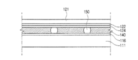
次いで、図4〜図7を参照してタッチスクリーンパネル100について詳しく説明する。
図4は、図3のA部分の拡大図であり、図5は、本発明の第1の実施形態による表示装置における第1の基板の配置図である。
図4及び図5を参照すると、第1の基板110は、第1の絶縁基板111、第1の絶縁基板111の上に形成される第1の抵抗膜112、第1の信号線113、第2の信号線114、第1の接続線115及び第2の接続線116を含む。
Next, the
FIG. 4 is an enlarged view of a portion A in FIG. 3, and FIG. 5 is a layout view of the first substrate in the display device according to the first embodiment of the present invention.
4 and 5, the
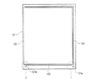
第1の絶縁基板111は大体長方形状であり、ガラスで構成されることができる。第1の絶縁基板111は第2の絶縁基板121より大きく、第2の絶縁基板121と重なり合わない第1の絶縁基板111の下辺にパッド領域B、Cが備えられている。
第1の抵抗膜112は、第1の絶縁基板111の上面の大部分にかけて形成されており、ITO(indium tin oxide)またはIZO(indium zinc oxide)のような透明電導物質で構成される。
The first
The
第1の信号線113と第2の信号線114とは第1の抵抗膜112を間に挟んで対向し、第1の絶縁基板111の長辺に沿って延長される。第1の信号線113及び第2の信号線114はX方向に延長されX信号線と称する。第1の信号線113及び第2の信号線114は第1の抵抗膜112と電気的に接続され、金属で構成される。
第1の信号線113の一端部は第1のパッド113aとなり、第1のパッド113aは第2の基板120により遮られない。第2の信号線114の一端部は第2のパッド114aとなり、第2のパッド114aは第2の基板120により遮られない
。
The
One end portion of the
第1の接続線115は、第2の基板120の第3の信号線123(図6参照)と電気的に接続され、第1の絶縁基板111の下辺に沿って形成される。第2の接続線116は、第2の基板120の第4の信号線124(図6参照)と電気的に接続され、第1の絶縁基板111の上辺及び左辺に沿って形成される。
第1の接続線115のうち、第2のパッド114aと近い端部は第3のパッド115aとなり、第3のパッド115aは第2の基板120により遮られない。第2の接続線116のうち、第1のパッド113aと近い端部は第4のパッド116aとなり、第4のパッド116aは第2の基板120により遮られない。
The
An end portion of the
このような実施形態とは異なり、各パッド113a〜116aは、接続される信号線(113、114)及び接続線(115、116)に比べ、幅が広げることができる。パッド113a〜116aは、一辺の長さが約1mm程度の正方形状として備えられることができる。
このようにパッド113a〜116aは二つの領域に備えられる。すなわち、第1の絶縁基板111の左下の角部の第1のパッド領域(B)に、第1のパッド113aと第4のパッド116aとが位置し、第1の絶縁基板111の右下の角部の第2のパッド領域(C)には、第2のパッド114aと第3のパッド115aとが位置する。
Unlike such an embodiment, the
In this manner, the
図6は、本発明の第1の実施形態による表示装置における第2の基板の配置図である。
図4及び図6を参照すれば、第2の基板120は、第2の絶縁基板121、第2の絶縁基板121の上に形成されている第2の抵抗膜122、第3の信号線123及び第4の信号線124を含む。
FIG. 6 is a layout view of the second substrate in the display device according to the first embodiment of the present invention.
Referring to FIGS. 4 and 6, the
第2の絶縁基板121は高分子フィルムで構成され、第1の絶縁基板111に比べ長さは短い。
第2の抵抗膜122は第2の絶縁基板111の下面の大部分にかけて形成されており、ITO(indium tin oxide)またはIZO(indium zinc oxide)のような透明導電物質で構成される。
The second
The
第3の信号線123と第4の信号線124とは、第2の抵抗膜122を間に挟んで対向し、第2の絶縁基板121の短辺に沿って延長される。第3の信号線123及び第4の信号線124はY方向に伸びてY信号線と称する。第3の信号線123及び第4の信号線124は第2の抵抗膜122と電気的に接続され、金属で構成される。
The
図7は、図6のVII−VII線に沿って切断した断面図である。
図7を参照すれば、第4の信号線124は金属で構成される導電部材150を通じて第2の接続線116と電気的に接続される。導電部材150は接着層140の間に不連続に形成される。図示してはいないが、第3の信号線123も同じ方式で第1の接続線115と電気的に接続される。
7 is a cross-sectional view taken along line VII-VII in FIG.
Referring to FIG. 7, the
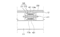
以下、図8及び図9を参照して、パッド113a〜116aとフレキシブル回路基板400との連結について説明する。
図8は、本発明の第1の実施形態による表示装置におけるフレキシブル回路基板の正面図であり、図9は、図2のIX−IX線に沿って切断した断面図である。
Hereinafter, the connection between the
FIG. 8 is a front view of the flexible circuit board in the display device according to the first embodiment of the present invention, and FIG. 9 is a cross-sectional view taken along the line IX-IX of FIG.
図8を参照すれば、フレキシブル回路基板400は、フレキシブルフィルム411、フレキシブルフィルム411の上に形成されている一対の接続配線を含む。
第1の接続配線は、入力リード421、出力リード423、両方のリード(421、423)を接続するリード接続部422を含む。第2の接続配線は、入力リード431、出力リード433、両方のリード(431、433)を接続するリード接続部432を含む。
第1の接続配線及び第2の接続配線は、フレキシブルフィルム411の同一面に形成されている。入力リード421、431は、第1の基板110のパッド113a〜116aに接続され、出力リード423、433は制御部300に電気的に接続される。
図示していないが、フレキシブル回路基板400は、リード接続部422、432を覆う絶縁フィルムをさらに含むことができる。
Referring to FIG. 8, the
The first connection wiring includes an
The first connection wiring and the second connection wiring are formed on the same surface of the
Although not shown, the
図9を参照すれば、第1のパッド113a及び第4のパッド116aは、第1のフレキシブル回路基板400aに接続される。第1のパッド113aは、異方性電導フィルム500を経て第1の接続配線の入力リード421と電気的に接続され、第4のパッド116aは、異方性電導フィルム500を経て第2の接続配線の入力リード431と電気的に接続される。
異方性電導フィルム500は、ベース樹脂部511と、ベース樹脂部511内に分散されている導電ボール512とを含む。パッド(113a、116a)と入力リード421、431との間に介在し、導電ボール512は互いに接触しながら電気的通路を形成する。
図示していないが、第2のパッド114a及び第3のパッド115aも同様に第2のフレキシブル回路基板400bに接続される。
Referring to FIG. 9, the
The anisotropic
Although not shown, the
第1の抵抗膜112の上には、スペーサ130が備えられる(図4参照)。スペーサ130は半球状であって、二つの抵抗膜(112、122)が短絡することを防止する。
第2の基板120の第2の絶縁基板121は高分子フィルムで製造されて、重力などによって第1の基板110に向かって変形しやすい。第2の基板120が変形すると、二つの抵抗膜(112、122)が短絡してユーザーの加圧の際、位置把握に問題が発生する。スペーサ130は、第2の基板120が変形しても、二つの抵抗膜(112、122)が直接接触することを防止する。
スペーサ130は、紫外線硬化材料または熱硬化材料などをスクリーンプリンティングまたは印刷して形成される。
接着層140(図3参照)はタッチパネルスクリーン100の周りに沿って配置されながら、両方の基板(110、120)を接着させる。接着層140は両面テープでなすことができる。
A
The second
The
The adhesive layer 140 (see FIG. 3) is disposed along the periphery of the
このようなタッチスクリーンパネル100において、ペンまたは指が第2の基板120を押し付けて第1の抵抗膜112と第2の抵抗膜122とが接触するようになると、その接触位置に応じて抵抗値が変わる。
可変抵抗値に応じて電流または電圧が変化し、その電流または電圧はパッド113a〜116aとフレキシブル回路基板400とを通じて出力される。フレキシブル回路基板400の出力リード423、433は直接、制御部300に接続されるか、液晶パネル200の駆動部(図示せず)に接続することができる。
In such a
The current or voltage changes according to the variable resistance value, and the current or voltage is output through the
再度、図2〜図4を参照しながら、液晶パネル200について説明する。
第1の液晶パネル基板210は、第3の絶縁基板211、薄膜トランジスタ212、絶縁膜213及び画素電極214を含む。
第3の絶縁基板211はガラスまたはプラスチックで構成できる。画素電極214は複数個で備えられており、それぞれ別途の薄膜トランジスタ212と電気的に接続している。
The
The first liquid
The third
第2の液晶パネル基板220は、第4の絶縁基板221、外部ブラックマトリックス222、内部ブラックマトリックス223、カラーフィルタ224、オーバーコート層225及び共通電極226を含む。
第4の絶縁基板221は、ガラスまたはプラスチックで構成できる。内部ブラックマトリックス223は、薄膜トランジスタ212に対応するように形成されている。カラーフィルタ224は、相異なる色相、たとえば、赤色、緑色及び青色を有する複数のサブ層を含む。共通電極226は、第4の絶縁基板221の全体にかけて形成されている。
The second liquid
The fourth insulating
画素電極214及び共通電極226は、ITO(indium tin oxide)またはIZO(indium zinc oxide)のような透明電導物質で構成される。
液晶層230は、画素電極214と共通電極226との間に形成される電界により整列状態を変化させながら、透過率を調節する。
第1の液晶パネル基板210の外面には、第1の偏光板240が取り付けられており、第2の液晶パネル基板220の外面には、第2の偏光板250が取り付けられている。
The
The
A first
第1の偏光板240は、接着剤(図示せず)を通じて第1の液晶パネル基板210の第3の絶縁基板211の背面に取り付けられる。第1の偏光板240は、入射される光の偏光状態を制御する偏光層と、その偏光層の上面及び下面に位置する支持層とを含む。
偏光層は、ポリビニルアルコール(Poly Vinyl Alcohol:PVA)の薄い膜をヨウ素化合物などの二色性染料溶液に浸すことによって染色し、加熱して一軸延伸することで形成される。
支持層はトリアセテートセルローズ(Tri−acetyl Cellulose:TAC)などで形成され、伸ばされた偏光層の収縮を防止し、偏光層を保護/支持する役割をする。
第2の偏光板250は、第1の偏光板240と同一構造を有するため、その説明を省略する。
図示してはいないが、表示装置1は、液晶パネル200の後方に位置するバックライトユニットをさらに含むことができる。
The first
The polarizing layer is formed by dyeing a thin film of polyvinyl alcohol (PVA) in a dichroic dye solution such as an iodine compound, heating, and uniaxially stretching.
The support layer is formed of triacetate cellulose (TAC) or the like, and prevents the stretched polarizing layer from contracting and serves to protect / support the polarizing layer.
Since the second
Although not shown, the
上述した第1の実施形態による表示装置において、タッチスクリーンパネル100のパッド113a〜116aには二つの領域に分けられてフレキシブル回路基板400a、400bが接続される。
したがって、各パッド領域B、C(図5を参照)を容易に備えることができるため、パッド領域の形成に必要な幅d1(図5を参照)は大きくない。したがって、タッチスクリーンパネル100のサイズが大きくなることを抑制する。
パッド領域B、C、信号線(113、114、123、124)及び接続線(115、116)は、液晶パネル200の外部ブラックマトリックス222より内の領域内に位置することが好ましい。
In the display device according to the first embodiment described above, the
Accordingly, the pad regions B and C (see FIG. 5) can be easily provided, and the width d1 (see FIG. 5) necessary for forming the pad region is not large. Therefore, an increase in the size of the
The pad regions B and C, the signal lines (113, 114, 123, and 124) and the connection lines (115 and 116) are preferably located in a region within the external
第1の基板110の信号線(113、114)及び接続線(115、116)の配置は様々に変更することができるが、これらを第2の実施形態及び第3の実施形態で説明する。
図10は、本発明の第2の実施形態による表示装置における第1の基板の配置図である。
第2の実施形態を示す図10を参照すると、第3の信号線123に接続される第1の接続線115の第3のパッド部115aは、第1のパッド部113aに隣接して形成される。
The arrangement of the signal lines (113, 114) and the connection lines (115, 116) of the
FIG. 10 is a layout view of the first substrate in the display device according to the second embodiment of the present invention.
Referring to FIG. 10 showing the second embodiment, the
第4の信号線124に接続される第2の接続線116は基板の上辺及び右辺に沿い、右辺部は第2の信号線114の後方に延長しており、第4のパッド部116aは第2のパッド部114aに隣接して形成されている。
第2の実施形態によれば、第1の絶縁基板111の左下の第1のパッド領域Dには、第1のパッド113aと第3のパッド115aとが位置し、右下の第2のパッド領域Eには、第2のパッド114aと第4のパッド116aとが位置する。
フレキシブル回路基板400と第1の基板110とは、第1の実施形態と同様に接続される。第1のフレキシブル回路基板400aは第1のパッド113a及び第3のパッド115aに接続され、第2のフレキシブル回路基板400bは第2のパッド114a及び第4のパッド116aに接続される。
The
According to the second embodiment, the
The
図11は、本発明の第3の実施形態による表示装置における第1の基板の配置図である。
第3の実施形態を示す図11を参照すると、第3の信号線123に接続される第1の信号線115の第3のパッド部115aは、第1のパッド部113aに隣接して形成されている。
また、第1のパッド部113a及び第3のパッド部115aは、第1の絶縁基板111の長辺(図11での左辺)に向けて形成されている。
第4の信号線124に接続される第2の接続線116は、第2の信号線114の後方に延長しており、第4のパッド部116aは第2のパッド部114aに隣接して形成されている。
第3の実施形態によれば、第1の絶縁基板111の左下の第1のパッド領域Fには、第1のパッド113a及び第3のパッド115aが位置し、右下の第2のパッド領域Gには、第2のパッド114a及び第4のパッド116aが位置する。
FIG. 11 is a layout view of a first substrate in the display device according to the third embodiment of the present invention.
Referring to FIG. 11 showing the third embodiment, the
Further, the
The
According to the third embodiment, the
また、フレキシブル回路基板400a、400bは、第1の絶縁基板111の相異なる辺に接続される。すなわち、第1のフレキシブル回路基板400aは、第1の絶縁基板111の長辺(左辺)に取り付けられながら、第1のパッド113a及び第3のパッド115aと接続される。一方、第2のフレキシブル回路基板400bは、第1の絶縁基板111の短辺(下辺)に取り付けられながら、第2のパッド114a及び第4のパッド116aと接続される。
The
次に、図12〜図18を参照しながら、第4の実施形態による表示装置について説明する。
図12は、本発明の第4の実施形態による表示装置の斜視図であり、図13は、図12のXIII−XIII線に沿って切断した断面図であり、図14は、図13のH部分の拡大図である。
図12〜図14を参照すると、液晶パネル200の第2の液晶パネル基板220は、タッチスクリーンパネル100の第1の基板110の第1の絶縁基板111を共有する。
Next, a display device according to a fourth embodiment will be described with reference to FIGS.
12 is a perspective view of a display device according to a fourth embodiment of the present invention, FIG. 13 is a cross-sectional view taken along line XIII-XIII in FIG. 12, and FIG. It is an enlarged view of a part.
12 to 14, the second liquid
すなわち、第1の絶縁基板111の上面には、第1の抵抗膜112が形成されており、第1の絶縁基板111の下面には、ブラックマトリックス(222、223)とカラーフィルタ224とが形成されている。
また、液晶パネル200の第2の偏光板250は、タッチスクリーンパネル100の上部に形成される。
第4の実施形態によれば、絶縁基板の使用を減らして表示装置1の厚さを減らすことができる。また、表示装置1の重さも減らすことができ、低コストも達成が可能である。
That is, the
Further, the second
According to the fourth embodiment, it is possible to reduce the thickness of the
図14及び図15を参照しながら、第1の基板110について説明する。
図15は、本発明の第4の実施形態による表示装置における第1の基板の配置図である。
第1の基板110は、第1の絶縁基板111、第1の絶縁基板111の上に形成されている第1の抵抗膜112、第1の信号線113及び第2の信号線114を含む。第1の実施形態とは異なり、第1の基板110に接続線は形成されない。
第1の抵抗膜112は、第1の絶縁基板111の上面の大部分にかけて形成されており、ITO(indium tin oxide)またはIZO(indium zinc oxide)のような透明電導物質で構成される。
The
FIG. 15 is a layout view of a first substrate in a display device according to the fourth embodiment of the present invention.
The
The
第1の信号線113と第2の信号線114とは抵抗膜112を間に挟んで対向し、第1の絶縁基板111の長辺に沿って延長される。第1の信号線113及び第2の信号線114は第1の抵抗膜112に電気的に接続され、金属で構成される。
第1の絶縁基板111の下辺に隣接する第1の信号線113の一端部は、第1のパッド113aとなり、第1の絶縁基板111の下辺に隣接する第2の信号線114の一端部は、第2のパッド114aとなる。
The
One end portion of the
図14及び図16を参照しながら、第2の基板120について説明する。
図16は、本発明の第4の実施形態による表示装置における第2の基板の配置図である。
第2の基板120は、第2の絶縁基板121、第2の絶縁基板121の上に形成されている第2の抵抗膜122、第3の信号線123及び第2の信号線124を含む。
第2の絶縁基板121は、その上部に第2の偏光板250が位置するので、伸びない等方性高分子フィルムで構成される。第2の絶縁基板121は、第1の絶縁基板111とほとんど同じ大きさを有する。
The
FIG. 16 is a layout view of a second substrate in the display device according to the fourth embodiment of the present invention.
The
The second
本実施形態とは異なり、第2の偏光板250の支持層上には第2の抵抗膜122を形成することができ、この場合、支持層が第2の絶縁基板121となる。
第3の信号線123は、第2の絶縁基板121の下辺に沿って延長され、第2の絶縁基板121の右辺(図16では第1の基板110と対向する面を正面として示しており左辺として示される)に隣接する端部が第3のパッド123aとなる。
第4の信号線124は、第2の絶縁基板121の上辺及び左辺(図16では右辺)に沿って延長され、第2の絶縁基板121の下辺に隣接する端部が第4のパッド124aとなる。
Unlike the present embodiment, the second
The
The
上述したように、第4の実施形態によれば、第1のパッド113a及び第2のパッド114aは第1の基板110に形成され、第3のパッド123a及び第4のパッド124aは第2の基板120に形成される。
第1の絶縁基板111の左下のパッド領域Iには、第1のパッド113a及び第4のパッド124aが備えられる。第1のパッド113aと第4のパッド124aとは互いに対向配置される。
第1の絶縁基板111の右下のパッド領域Jには、第2のパッド114a及び第3のパッド123aが備えられる。第2のパッド114aと第3のパッド123aとは互いに対向配置される。
このようにパッド(113a、114a、123a、124a)は、タッチスクリーンパネル100の両方の角部の二つの領域に備えられる。
As described above, according to the fourth embodiment, the
In the lower left pad region I of the first insulating
In the lower right pad region J of the first insulating
Thus, the pads (113a, 114a, 123a, 124a) are provided in two regions at both corners of the
図17(a)〜(c)及び図18を参照しながら、パッド(113a、114a、123a、124a)とフレキシブル回路基板400との接続を説明する。
図17(a)〜(c)は、本発明の第4の実施形態による表示装置におけるフレキシブル回路基板を示す図であり、(a)は正面図、(b)は裏面図、(c)は(a)のXVIIc−XVIIc線に沿って切断した断面図である。
図18は、図12のXVIII−XVIII線に沿って切断した断面図である。
The connection between the pads (113a, 114a, 123a, 124a) and the
17A to 17C are diagrams showing a flexible circuit board in a display device according to the fourth embodiment of the present invention, where FIG. 17A is a front view, FIG. 17B is a back view, and FIG. It is sectional drawing cut | disconnected along the XVIIc-XVIIc line | wire of (a).
18 is a cross-sectional view taken along line XVIII-XVIII in FIG.
図17(a)〜(c)を参照すると、フレキシブル回路基板400は、フレキシブルフィルム411、フレキシブルフィルム411の上に形成されている一対の接続配線を含む。
第1の接続配線は、入力リード421、出力リード423、両方のリード(421、423)を接続するリード接続部422を含む。第2の接続配線は、入力リード431、出力リード433、両方のリード(431、433)を接続するリード接続部432を含む。
Referring to FIGS. 17A to 17C, the
The first connection wiring includes an
フレキシブル回路基板400は両面フレキシブル回路基板である。入力リード421、出力リード423、リード接続部422及び出力リード433は、フレキシブルフィルム411の第1の面411aに形成されており、第2の接続配線の入力リード431は、フレキシブルフィルム411の第2の面411bに形成されている。
第2の接続配線のリード接続部432の一部は出力リード433に接続されて第1の面411aに形成されており、他の一部は入力リード431に接続されて第2の面411bに形成されている。相異なる面に形成されているリード接続部432は、フレキシブルフィルム411に形成されているビア(via)412を通じて相互に接続される。
The
A part of the
図18を参照すると、第1のパッド113a及び第4のパッド124aは、第1のフレキシブル回路基板400aに接続されている。第1のパッド113aは、異方性電導フィルム500を通じて第2の接続配線の入力リード431に電気的に接続され、第4のパッド124aは、異方性電導フィルム500を通じて第1の接続配線の入力リード421に電気的に接続される。
異方性電導フィルム500は、ベース樹脂部511及びベース樹脂部511内に分散されている導電ボール512を含む。パッド(113a、124a)とリード(421、431)との間で、導電ボール512は互いに接触しながら、電気的通路を形成する。
図示していないが、第2のパッド114a及び第3のパッド123aも、これと同様の方式で第2のフレキシブル回路基板400bに接続される。
図18において、第1の絶縁基板111の下部の液晶パネル200はその図示を省略した。
Referring to FIG. 18, the
The anisotropic
Although not shown, the
In FIG. 18, the illustration of the
上述した第4の実施形態によれば、各パッド領域I、Jにおいて、パッド(113a、114a、123a、124a)は二つずつ備えられるが、互いに垂直方向に重畳しているため、一つのパッドの設置に必要な面積のみが必要である。従って、タッチスクリーンパネル100のサイズ増加の抑制に有利である。
第4の実施形態において、パッド領域I、Jは、外部ブラックマトリックス222の領域内に位置する。外部ブラックマトリックス222の幅d2(図15参照)は、2mm程度とすることができる。
According to the fourth embodiment described above, two pads (113a, 114a, 123a, 124a) are provided in each pad region I, J, but one pad is overlapped with each other in the vertical direction. Only the area required for the installation is required. Therefore, it is advantageous for suppressing an increase in the size of the
In the fourth embodiment, the pad areas I and J are located in the area of the external
第4の実施形態において、信号線(113、114、123、124)の配置は様々に変更することができるが、これは第5の実施形態として説明する。
図19は、本発明の第5の実施形態による表示装置における第1の基板の配置図である。
図19を参照すると、第2の信号線114は、第1の絶縁基板111の右辺及び下辺に延長され、第1のパッド113aに隣接する第2のパッド114aを有する。
図20を参照すれば、第4の信号線124は、第2の絶縁基板121の上辺及び左辺に延長され、第3のパッド123aに隣接する第4のパッド124aを有する。
In the fourth embodiment, the arrangement of the signal lines (113, 114, 123, and 124) can be variously changed. This will be described as a fifth embodiment.
FIG. 19 is a layout view of the first substrate in the display device according to the fifth embodiment of the present invention.
Referring to FIG. 19, the
Referring to FIG. 20, the
第5の実施形態において、パッド領域Kには、第1の基板110のパッド(113a、114a)が位置し、パッド部Jには、第2の基板120のパッド(123a、124a)が位置する。
したがって、第5の実施形態において、フレキシブル回路基板400としては単面フレキシブル回路基板が用いられる。第1のフレキシブル回路基板400aは第1の基板110に取り付けられて第1のパッド113a及び第2のパッド114aに接続され、第2のフレキシブル回路基板400bは第2の基板120に取り付けられて第3のパッド123a及び第4のパッド124aに接続される。
In the fifth embodiment, the pads (113a, 114a) of the
Therefore, in the fifth embodiment, a single-sided flexible circuit board is used as the
次に、図21〜図25を参照しながら、第6の実施形態について説明する。
図21は、本発明の第6の実施形態による表示装置の斜視図であり、図22は、本発明の第6の実施形態による表示装置における第1の基板の配置図であり、図23は、本発明の第6の実施形態による表示装置における第2の基板の配置図である。
図24は、本発明の第6の実施形態による表示装置におけるフレキシブル回路基板を示す図であり、(a)は正面図、(b)は裏面図である。
図25は、図21のXXV−XXV線に沿って切断した断面図である。
Next, a sixth embodiment will be described with reference to FIGS.
FIG. 21 is a perspective view of a display device according to the sixth embodiment of the present invention, FIG. 22 is a layout diagram of a first substrate in the display device according to the sixth embodiment of the present invention, and FIG. FIG. 10 is a layout view of a second substrate in a display device according to a sixth embodiment of the present invention.
24A and 24B are diagrams showing a flexible circuit board in a display device according to a sixth embodiment of the present invention, in which FIG. 24A is a front view and FIG. 24B is a back view.
25 is a cross-sectional view taken along the line XXV-XXV in FIG.
図21を参照すると、第6の実施形態において、単一のフレキシブル回路基板400が備えられる。
図22及び図23を参照すると、各パッド(113a、114a、123a、124a)は互いに隣接し、第1の基板110のパッド(113a、114a)と第2の基板120のパッド(123a、124a)とが互いに重畳するように備えられている。すなわち、単一のパッド領域Mが備えられる。これにより、単一のフレキシブル回路基板400が形成される。
Referring to FIG. 21, in the sixth embodiment, a single
22 and 23, each pad (113a, 114a, 123a, 124a) is adjacent to each other, and the pad (113a, 114a) of the
図24(a)及び(b)を参照すると、フレキシブル回路基板400は両面回路基板で4本の接続配線が備えられる。
第1の接続配線は、入力リード421、出力リード423、両方のリード(421、423)を接続するリード接続部422を含む。第2の接続配線は、入力リード431、出力リード433、両方のリード(431、433)を接続するリード接続部432を含む。第3の接続配線は、入力リード441、出力リード443、両方のリード(441、443)を接続するリード接続部442を含む。第4の接続配線は、入力リード451、出力リード453、両方のリード(451、453)を接続するリード接続部452を含む。
Referring to FIGS. 24A and 24B, the
The first connection wiring includes an
このうち、第3の接続配線の入力リード441と第4の接続配線の入力リード451とは、第2の面411bに備えられ、第3の接続配線のリード接続部442の一部と第4の接続配線のリード接続部452の一部とも、第2の面411bに備えられる。
第1の面411aに備えられるリード接続部442、452と第2の面411bに位置するリード接続部442、452とは、フレキシブルフィルム411に形成されるビア(図示せず)を通じて接続される。
Among these, the
The
図25を参照すれば、第1のパッド113aは、異方性電導フィルム500を通じて第4の接続配線の入力リード451に電気的に接続され、第2のパッド114aは、異方性電導フィルム500を通じて第3の接続配線の入力リード441に電気的に接続される。
また、第3のパッド123aは、第2の接続配線の入力リード431に電気的に接続され、第4のパッド124aは、第1の接続配線の入力リード421に電気的に接続される。
図25においては、第1の絶縁基板111の下部の液晶パネル200はその図示を省略した。
第6の実施形態によれば、パッド領域の面積を減らすのみならず、フレキシブル回路基板400の個数も減らすことができる。
Referring to FIG. 25, the
The
In FIG. 25, the
According to the sixth embodiment, not only the area of the pad region can be reduced, but also the number of
以上の第4の実施形態及び第6の実施形態において説明した両面フレキシブル回路基板を用いる構造は、第1の実施形態でのようにタッチスクリーンパネル100と液晶パネル200とを分離した構造にも適用することができる。
本発明において、フレキシブル回路基板400の取り付け位置は、タッチスクリーンパネル100の角領域に限られない。また、本発明は5本以上の信号線を有する構造にも適用が可能であるが、信号線が5本の場合、信号線を2本と3本にわけてフレキシブル回路基板に接続することができる。信号線が5本以上の場合、三つ以上のフレキシブル回路基板を用いることもできる。
The structure using the double-sided flexible circuit board described in the fourth and sixth embodiments is also applicable to a structure in which the
In the present invention, the mounting position of the
尚、本発明は、上述の実施形態に限られるものではない。本発明の技術的範囲から逸脱しない範囲内で多様に変更実施することが可能である。 The present invention is not limited to the embodiment described above. Various modifications can be made without departing from the technical scope of the present invention.
100 タッチスクリーンパネル
110 第1の基板
111 第1の絶縁基板
112 第1の抵抗膜
113 第1の信号線
113a 第1のパッド
114 第2の信号線
114a 第2のパッド
115 第1の接続線
115a 第3のパッド
116 第2の接続線
116a 第4のパッド
120 第2の基板
121 第2の絶縁基板
122 第2の抵抗膜
123 第3の信号線
124 第4の信号線
130 スペーサ
140 接着層
150 導電部材
200 液晶パネル
210、220 (第1及び第2の)液晶パネル基板
212 薄膜トランジスタ
214 画素電極
222、223 (外部及び内部)ブラックマトリックス
224 カラーフィルタ
225 オーバーコート
226 共通電極
230 液晶層
240、250 (第1及び第2の)偏光板
260 シーラント
300 制御部
400 フレキシブル回路基板
411 フレキシブルフィルム
400a、400b (第1及び第2の)フレキシブル回路基板
421、431、441、451 入力リード
422、432、442、452 リード接続部
423、433、443、453 出力リード
500 異方性電導フィルム
511 ベース樹脂部
512 導電ボール
DESCRIPTION OF
Claims (11)
前記第1の基板と対向し、第2の絶縁基板と、前記第2の絶縁基板上に形成される第2の抵抗膜と、前記第2の絶縁基板上に形成される第3の信号線及び第4の信号線とを含む第2の基板と、
前記第1の信号線の端部に接続される第1のパッドと、前記第2の信号線の端部に接続される第2のパッドと、第1の接続線の端部に接続される第3のパッドと、第2の接続線の端部に接続される第4のパッドと、を含むパッド部と、
前記各々のパッドの内のいずれか二つに接続される第1のフレキシブル回路基板と、
前記各々のパッドのうちの他方の二つに接続される第2のフレキシブル回路基板と、を有し、
前記第1の絶縁基板の第1のパッド領域に、前記第1のパッドと前記第4のパッドとが位置し、前記第1の絶縁基板の第2のパッド領域には、前記第2のパッドと前記第3のパッドとが位置し、
前記第1の基板は前記第2の基板より大きく、前記第2の基板と重なり合わない前記第1の基板の領域に前記第1及び第2のパッド領域を備え、
前記第1乃至第4のパッドは第2の基板により遮られず、
前記第1乃至第4のパッドは、前記第1のフレキシブル回路基板と、前記第2のフレキシブル回路基板とが、前記第1の絶縁基板の同一の辺から出るように形成され、
前記第1及び第2のパッド領域は、前記第1の絶縁基板の同一の辺の相異なる角部に位置し、
前記第1の接続線は、導電部材により前記第2の基板の前記第3の信号線と電気的に接続され、前記第1の絶縁基板の下辺に沿って形成され、
前記第2の接続線は、導電部材により前記第2の基板の前記第4の信号線と電気的に接続され、前記第1の絶縁基板の上辺及び左辺に沿って形成され、
ペンまたは指が前記第2の基板を押し付けて前記第1の抵抗膜と前記第2の抵抗膜とが接触するようになると、その接触位置に応じて抵抗値が変わることに応じて、電流または電圧が変化することにより、接触を検知するタッチスクリーンパネルと、表示パネルとを含むことを特徴とする表示装置。 A rectangular first insulating substrate, a first resistance film formed on the first insulating substrate, a first signal line and a second signal formed on the first insulating substrate A first substrate including a line;
Opposing to the first substrate, a second insulating substrate, a second resistance film formed on the second insulating substrate, and a third signal line formed on the second insulating substrate And a second substrate including a fourth signal line;
A first pad connected to an end of the first signal line, a second pad connected to an end of the second signal line, and an end of the first connection line A pad portion including a third pad and a fourth pad connected to an end of the second connection line;
A first flexible circuit board connected to any two of the pads;
A second flexible circuit board connected to the other two of the pads,
The first pad and the fourth pad are located in a first pad region of the first insulating substrate, and the second pad is located in a second pad region of the first insulating substrate. And the third pad are located,
The first substrate is larger than the second substrate and includes the first and second pad regions in a region of the first substrate that does not overlap the second substrate;
The first to fourth pads are not blocked by the second substrate,
The first to fourth pads are formed such that the first flexible circuit board and the second flexible circuit board come out of the same side of the first insulating substrate,
The first and second pad regions are located at different corners of the same side of the first insulating substrate,
The first connection line is electrically connected to the third signal line of the second substrate by a conductive member, and is formed along the lower side of the first insulating substrate,
The second connection line is electrically connected to the fourth signal line of the second substrate by a conductive member, and is formed along the upper side and the left side of the first insulating substrate,
When the pen or finger presses the second substrate and the first resistance film and the second resistance film come into contact with each other, the current or the resistance value changes according to the contact position. A display device comprising: a touch screen panel that detects contact when a voltage changes; and a display panel.
前記第1の液晶パネル基板に対向し、外部ブラックマトリックスが形成される第2の液晶パネル基板と、
前記第1及び第2の液晶パネル基板の間に介在する液晶層とを含み、
前記パッド部は、前記外部ブラックマトリックス領域内に配置されることを特徴とする請求項5に記載の表示装置。 The liquid crystal panel includes a first liquid crystal panel substrate on which a thin film transistor is formed;
A second liquid crystal panel substrate facing the first liquid crystal panel substrate and having an external black matrix formed thereon;
A liquid crystal layer interposed between the first and second liquid crystal panel substrates,
The display device according to claim 5, wherein the pad unit is disposed in the external black matrix region.
前記第1の絶縁基板と前記液晶パネル基板との間に介在する液晶層とをさらに有することを特徴とする請求項1に記載の表示装置。 A liquid crystal panel substrate on which a thin film transistor is formed facing the back surface of the first insulating substrate;
The display device according to claim 1, further comprising a liquid crystal layer interposed between the first insulating substrate and the liquid crystal panel substrate.
前記パッド部は、前記外部ブラックマトリックス領域内に配置されることを特徴とする請求項8に記載の表示装置。 An external black matrix formed on the back surface of the first insulating substrate;
The display device according to claim 8, wherein the pad unit is disposed in the external black matrix region.
The display device according to claim 8, wherein the second insulating substrate is a polymer film.
Applications Claiming Priority (2)
| Application Number | Priority Date | Filing Date | Title |
|---|---|---|---|
| KR1020060131913A KR101330697B1 (en) | 2006-12-21 | 2006-12-21 | Display device |
| KR10-2006-0131913 | 2006-12-21 |
Publications (3)
| Publication Number | Publication Date |
|---|---|
| JP2008158487A JP2008158487A (en) | 2008-07-10 |
| JP2008158487A5 JP2008158487A5 (en) | 2010-08-19 |
| JP5732185B2 true JP5732185B2 (en) | 2015-06-10 |
Family
ID=39542268
Family Applications (1)
| Application Number | Title | Priority Date | Filing Date |
|---|---|---|---|
| JP2007177185A Expired - Fee Related JP5732185B2 (en) | 2006-12-21 | 2007-07-05 | Display device |
Country Status (4)
| Country | Link |
|---|---|
| US (2) | US8223278B2 (en) |
| JP (1) | JP5732185B2 (en) |
| KR (1) | KR101330697B1 (en) |
| CN (1) | CN101206326A (en) |
Families Citing this family (59)
| Publication number | Priority date | Publication date | Assignee | Title |
|---|---|---|---|---|
| US9128525B2 (en) | 2008-01-04 | 2015-09-08 | Tactus Technology, Inc. | Dynamic tactile interface |
| US9052790B2 (en) | 2008-01-04 | 2015-06-09 | Tactus Technology, Inc. | User interface and methods |
| US9552065B2 (en) | 2008-01-04 | 2017-01-24 | Tactus Technology, Inc. | Dynamic tactile interface |
| US9298261B2 (en) | 2008-01-04 | 2016-03-29 | Tactus Technology, Inc. | Method for actuating a tactile interface layer |
| US8243038B2 (en) | 2009-07-03 | 2012-08-14 | Tactus Technologies | Method for adjusting the user interface of a device |
| US8922503B2 (en) | 2008-01-04 | 2014-12-30 | Tactus Technology, Inc. | User interface system |
| US9557915B2 (en) | 2008-01-04 | 2017-01-31 | Tactus Technology, Inc. | Dynamic tactile interface |
| US9063627B2 (en) | 2008-01-04 | 2015-06-23 | Tactus Technology, Inc. | User interface and methods |
| US8456438B2 (en) | 2008-01-04 | 2013-06-04 | Tactus Technology, Inc. | User interface system |
| US9612659B2 (en) | 2008-01-04 | 2017-04-04 | Tactus Technology, Inc. | User interface system |
| US20160187981A1 (en) | 2008-01-04 | 2016-06-30 | Tactus Technology, Inc. | Manual fluid actuator |
| US8547339B2 (en) | 2008-01-04 | 2013-10-01 | Tactus Technology, Inc. | System and methods for raised touch screens |
| US9274612B2 (en) | 2008-01-04 | 2016-03-01 | Tactus Technology, Inc. | User interface system |
| US8154527B2 (en) | 2008-01-04 | 2012-04-10 | Tactus Technology | User interface system |
| US8970403B2 (en) | 2008-01-04 | 2015-03-03 | Tactus Technology, Inc. | Method for actuating a tactile interface layer |
| US9372565B2 (en) | 2008-01-04 | 2016-06-21 | Tactus Technology, Inc. | Dynamic tactile interface |
| US9423875B2 (en) | 2008-01-04 | 2016-08-23 | Tactus Technology, Inc. | Dynamic tactile interface with exhibiting optical dispersion characteristics |
| US9720501B2 (en) | 2008-01-04 | 2017-08-01 | Tactus Technology, Inc. | Dynamic tactile interface |
| US9588683B2 (en) | 2008-01-04 | 2017-03-07 | Tactus Technology, Inc. | Dynamic tactile interface |
| US8928621B2 (en) | 2008-01-04 | 2015-01-06 | Tactus Technology, Inc. | User interface system and method |
| US8947383B2 (en) | 2008-01-04 | 2015-02-03 | Tactus Technology, Inc. | User interface system and method |
| US8922510B2 (en) | 2008-01-04 | 2014-12-30 | Tactus Technology, Inc. | User interface system |
| US8928597B2 (en) | 2008-07-11 | 2015-01-06 | Samsung Display Co., Ltd. | Organic light emitting display device |
| US9342176B2 (en) | 2008-07-21 | 2016-05-17 | Samsung Display Co., Ltd. | Organic light emitting display device |
| US9588684B2 (en) | 2009-01-05 | 2017-03-07 | Tactus Technology, Inc. | Tactile interface for a computing device |
| US9740341B1 (en) | 2009-02-26 | 2017-08-22 | Amazon Technologies, Inc. | Capacitive sensing with interpolating force-sensitive resistor array |
| US10180746B1 (en) * | 2009-02-26 | 2019-01-15 | Amazon Technologies, Inc. | Hardware enabled interpolating sensor and display |
| JP5436935B2 (en) * | 2009-05-28 | 2014-03-05 | 株式会社ジャパンディスプレイ | Liquid crystal display |
| JP5584433B2 (en) | 2009-06-17 | 2014-09-03 | 株式会社ジャパンディスプレイ | Liquid crystal display |
| CN105260110A (en) | 2009-07-03 | 2016-01-20 | 泰克图斯科技公司 | User interface enhancement system |
| US9244562B1 (en) | 2009-07-31 | 2016-01-26 | Amazon Technologies, Inc. | Gestures and touches on force-sensitive input devices |
| US9785272B1 (en) | 2009-07-31 | 2017-10-10 | Amazon Technologies, Inc. | Touch distinction |
| KR101058106B1 (en) * | 2009-08-06 | 2011-08-24 | 삼성모바일디스플레이주식회사 | Display device |
| US8810524B1 (en) | 2009-11-20 | 2014-08-19 | Amazon Technologies, Inc. | Two-sided touch sensor |
| WO2011087816A1 (en) * | 2009-12-21 | 2011-07-21 | Tactus Technology | User interface system |
| US9239623B2 (en) | 2010-01-05 | 2016-01-19 | Tactus Technology, Inc. | Dynamic tactile interface |
| WO2011112984A1 (en) | 2010-03-11 | 2011-09-15 | Tactus Technology | User interface system |
| KR20130136905A (en) | 2010-04-19 | 2013-12-13 | 택투스 테크놀로지, 아이엔씨. | User interface system |
| KR101756656B1 (en) * | 2010-06-25 | 2017-07-11 | 엘지디스플레이 주식회사 | Organic light emitting diode display device including touch panel |
| US20120075823A1 (en) * | 2010-09-28 | 2012-03-29 | Samsung Electronics Co. Ltd. | Display panel and method of manufacturing the same |
| JP5647353B2 (en) | 2010-10-20 | 2014-12-24 | タクタス テクノロジーTactus Technology | User interface system |
| US20130329350A1 (en) * | 2011-02-23 | 2013-12-12 | Ntt Docomo, Inc. | Electronic apparatus |
| KR101908501B1 (en) * | 2011-12-07 | 2018-10-17 | 엘지디스플레이 주식회사 | Integrated Touch Screen With Organic Emitting Display Device and Method for Manufacturing the Same |
| CN102869186B (en) * | 2012-04-26 | 2015-07-29 | 宸阳光电科技(厦门)有限公司 | A kind of flexible print circuit board and touch screen syndeton |
| KR101925609B1 (en) * | 2012-06-15 | 2018-12-06 | 삼성디스플레이 주식회사 | Display device |
| CN104662497A (en) | 2012-09-24 | 2015-05-27 | 泰克图斯科技公司 | Dynamic tactile interface and methods |
| US9405417B2 (en) | 2012-09-24 | 2016-08-02 | Tactus Technology, Inc. | Dynamic tactile interface and methods |
| CN103226427A (en) * | 2012-11-30 | 2013-07-31 | 深圳市骏达光电有限公司 | FPC for resistive touch screen, resistive touch screen, and electronic equipment |
| US9557813B2 (en) | 2013-06-28 | 2017-01-31 | Tactus Technology, Inc. | Method for reducing perceived optical distortion |
| TWM511619U (en) * | 2015-08-28 | 2015-11-01 | Nano Bit Tech Co Ltd | Optical composite layer structure |
| JP2018017986A (en) * | 2016-07-29 | 2018-02-01 | 株式会社ジャパンディスプレイ | Display device |
| KR102655712B1 (en) * | 2016-09-07 | 2024-04-11 | 삼성디스플레이 주식회사 | Display device and method for manufacturing the same |
| CN106648209B (en) * | 2016-10-19 | 2019-10-25 | 武汉华星光电技术有限公司 | Flexible touch screen and preparation method thereof, touching device |
| CN106773386B (en) * | 2016-12-23 | 2020-09-01 | 武汉华星光电技术有限公司 | Double-sided display device |
| CN106681042B (en) * | 2017-01-05 | 2021-01-26 | 京东方科技集团股份有限公司 | Touch display screen, manufacturing method thereof and touch display device |
| TWI622911B (en) * | 2017-02-14 | 2018-05-01 | 宏碁股份有限公司 | Touch apparatus |
| CN108459773A (en) * | 2018-04-10 | 2018-08-28 | 江苏聚泰科技有限公司 | A kind of display device of novel liquid crystal touch screen |
| KR20200026369A (en) * | 2018-08-30 | 2020-03-11 | 삼성디스플레이 주식회사 | Display device |
| CN110597416B (en) * | 2019-09-17 | 2021-08-17 | 京东方科技集团股份有限公司 | Flexible circuit board, touch display panel and touch display device |
Family Cites Families (24)
| Publication number | Priority date | Publication date | Assignee | Title |
|---|---|---|---|---|
| JP3205373B2 (en) * | 1992-03-12 | 2001-09-04 | 株式会社日立製作所 | Liquid crystal display |
| US5628031A (en) * | 1993-07-19 | 1997-05-06 | Elonex Ip Holdings Ltd. | Personal digital assistant module implemented as a low-profile printed circuit assembly having a rigid substrate wherein IC devices are mounted within openings wholly between opposite plane surfaces of the rigid substrate |
| JPH1011204A (en) * | 1996-06-27 | 1998-01-16 | Toshiba Corp | Coordinate input device using tablet |
| JPH10312244A (en) * | 1997-05-13 | 1998-11-24 | Seiko Epson Corp | Liquid crystal display device with input device |
| JP2000020226A (en) | 1998-07-06 | 2000-01-21 | Alps Electric Co Ltd | Coordinate input device |
| TW523627B (en) * | 1998-07-14 | 2003-03-11 | Hitachi Ltd | Liquid crystal display device |
| JP3161528B2 (en) * | 1998-09-07 | 2001-04-25 | 日本電気株式会社 | LCD panel |
| KR100505201B1 (en) * | 2000-10-13 | 2005-07-29 | 가부시키가이샤 덴소 | Touch panel and method of manufacturing touch panel |
| JP2002182854A (en) * | 2000-12-18 | 2002-06-28 | Hitachi Ltd | Touch panel and image input type display device |
| US7255451B2 (en) * | 2002-09-20 | 2007-08-14 | Donnelly Corporation | Electro-optic mirror cell |
| US20020149571A1 (en) * | 2001-04-13 | 2002-10-17 | Roberts Jerry B. | Method and apparatus for force-based touch input |
| CN100378551C (en) * | 2001-10-22 | 2008-04-02 | 三星电子株式会社 | Liquid crystal display and its manufacture method |
| US7253808B2 (en) * | 2002-11-18 | 2007-08-07 | Lg.Philips Lcd Co., Ltd. | Touch screen system and display device using the same |
| US7499038B2 (en) | 2002-12-10 | 2009-03-03 | Nissha Printing Co., Ltd. | Thin-frame touch panel |
| CN1316294C (en) | 2002-12-10 | 2007-05-16 | 统宝光电股份有限公司 | Planar display with touch panel |
| JP4016955B2 (en) * | 2003-05-02 | 2007-12-05 | セイコーエプソン株式会社 | ELECTRO-OPTICAL DEVICE, MANUFACTURING METHOD THEREOF, AND ELECTRONIC DEVICE |
| KR101209489B1 (en) * | 2003-08-22 | 2012-12-07 | 엘지디스플레이 주식회사 | Liquid crystal display device |
| KR101002307B1 (en) * | 2003-12-04 | 2010-12-20 | 엘지디스플레이 주식회사 | Liquid Crystal Display and Fabricating Method thereof |
| JP2006091059A (en) * | 2004-09-21 | 2006-04-06 | Seiko Epson Corp | Electrooptical device, manufacturing method for electrooptical device, and electronic equipment |
| US7439962B2 (en) * | 2005-06-01 | 2008-10-21 | Synaptics Incorporated | Touch pad with flexible substrate |
| US7582556B2 (en) * | 2005-06-24 | 2009-09-01 | Megica Corporation | Circuitry component and method for forming the same |
| TWI298989B (en) * | 2005-12-01 | 2008-07-11 | Au Optronics Corp | Circuit board module and forming ethod thereof |
| KR101205535B1 (en) * | 2005-12-06 | 2012-11-27 | 삼성디스플레이 주식회사 | Apparatus for driving of light source and display device having the same and method of driving of light source |
| KR100770921B1 (en) * | 2006-04-25 | 2007-10-26 | 삼성전자주식회사 | Keypad assembly for mobile phone |
-
2006
- 2006-12-21 KR KR1020060131913A patent/KR101330697B1/en not_active IP Right Cessation
-
2007
- 2007-07-05 JP JP2007177185A patent/JP5732185B2/en not_active Expired - Fee Related
- 2007-11-07 US US11/936,253 patent/US8223278B2/en not_active Expired - Fee Related
- 2007-12-07 CN CNA2007101988028A patent/CN101206326A/en active Pending
-
2012
- 2012-05-18 US US13/474,923 patent/US8488071B2/en not_active Expired - Fee Related
Also Published As
| Publication number | Publication date |
|---|---|
| CN101206326A (en) | 2008-06-25 |
| US20080151171A1 (en) | 2008-06-26 |
| US8223278B2 (en) | 2012-07-17 |
| KR101330697B1 (en) | 2013-11-18 |
| JP2008158487A (en) | 2008-07-10 |
| US20120229717A1 (en) | 2012-09-13 |
| KR20080057953A (en) | 2008-06-25 |
| US8488071B2 (en) | 2013-07-16 |
Similar Documents
| Publication | Publication Date | Title |
|---|---|---|
| JP5732185B2 (en) | Display device | |
| KR102373330B1 (en) | Display device and driving method thereof | |
| US11335739B2 (en) | Display panel and display device | |
| US20210132738A1 (en) | Flat panel display with integrated touch screen panel | |
| US9857903B2 (en) | In-cell OLED touch display structure with high light penetration rate | |
| KR102035005B1 (en) | Touch display device | |
| TWI429984B (en) | Touch panel-integrated liquid crystal display device | |
| JP2019220214A (en) | Display device including touch sensor | |
| US11009732B2 (en) | Display panel and display device | |
| EP2960760B1 (en) | Touch panel with a printing layer of a certain surface roughness | |
| TWI539342B (en) | Touch sensor built-in display device and terminal connection structure | |
| WO2010058495A1 (en) | Touch panel and display device using the same | |
| JP2008134975A (en) | Input device and its manufacturing method | |
| KR20130072635A (en) | Display device integrated touch screen panel | |
| JP2014211825A (en) | Display device | |
| US20150085208A1 (en) | In-cell touch display structure | |
| US20190121475A1 (en) | Touch sensor integrated color filter and manufacturing method for the same | |
| JP6097663B2 (en) | Display device with built-in touch panel function | |
| KR101658149B1 (en) | Display Device Including Touch Panel | |
| TWM492475U (en) | Embedded display touch-control structure | |
| US11188164B2 (en) | Display device | |
| KR20210101359A (en) | Electronic panel and display device comprising the same | |
| US10795482B2 (en) | Touch panel and electronic device | |
| US10564767B2 (en) | Display device | |
| KR102305463B1 (en) | Display device including touch sensor and driving method thereof |
Legal Events
| Date | Code | Title | Description |
|---|---|---|---|
| A521 | Written amendment |
Free format text: JAPANESE INTERMEDIATE CODE: A523 Effective date: 20100705 |
|
| A621 | Written request for application examination |
Free format text: JAPANESE INTERMEDIATE CODE: A621 Effective date: 20100705 |
|
| A521 | Written amendment |
Free format text: JAPANESE INTERMEDIATE CODE: A523 Effective date: 20110629 |
|
| A977 | Report on retrieval |
Free format text: JAPANESE INTERMEDIATE CODE: A971007 Effective date: 20120411 |
|
| A131 | Notification of reasons for refusal |
Free format text: JAPANESE INTERMEDIATE CODE: A131 Effective date: 20120417 |
|
| A521 | Written amendment |
Free format text: JAPANESE INTERMEDIATE CODE: A523 Effective date: 20120717 |
|
| A711 | Notification of change in applicant |
Free format text: JAPANESE INTERMEDIATE CODE: A712 Effective date: 20121213 |
|
| A131 | Notification of reasons for refusal |
Free format text: JAPANESE INTERMEDIATE CODE: A131 Effective date: 20130312 |
|
| A521 | Written amendment |
Free format text: JAPANESE INTERMEDIATE CODE: A523 Effective date: 20130612 |
|
| A02 | Decision of refusal |
Free format text: JAPANESE INTERMEDIATE CODE: A02 Effective date: 20130806 |
|
| A521 | Written amendment |
Free format text: JAPANESE INTERMEDIATE CODE: A523 Effective date: 20131129 |
|
| A911 | Transfer of reconsideration by examiner before appeal (zenchi) |
Free format text: JAPANESE INTERMEDIATE CODE: A911 Effective date: 20131209 |
|
| A912 | Removal of reconsideration by examiner before appeal (zenchi) |
Free format text: JAPANESE INTERMEDIATE CODE: A912 Effective date: 20140124 |
|
| A521 | Written amendment |
Free format text: JAPANESE INTERMEDIATE CODE: A523 Effective date: 20141203 |
|
| A521 | Written amendment |
Free format text: JAPANESE INTERMEDIATE CODE: A523 Effective date: 20150227 |
|
| A61 | First payment of annual fees (during grant procedure) |
Free format text: JAPANESE INTERMEDIATE CODE: A61 Effective date: 20150413 |
|
| R150 | Certificate of patent or registration of utility model |
Ref document number: 5732185 Country of ref document: JP Free format text: JAPANESE INTERMEDIATE CODE: R150 |
|
| LAPS | Cancellation because of no payment of annual fees |