JP5728443B2 - Electromechanical device - Google Patents

Electromechanical device Download PDF

Info

Publication number
JP5728443B2
JP5728443B2 JP2012181666A JP2012181666A JP5728443B2 JP 5728443 B2 JP5728443 B2 JP 5728443B2 JP 2012181666 A JP2012181666 A JP 2012181666A JP 2012181666 A JP2012181666 A JP 2012181666A JP 5728443 B2 JP5728443 B2 JP 5728443B2
Authority
JP
Japan
Prior art keywords
layer
shutter
aperture
deposited
substrate
Prior art date
Legal status (The legal status is an assumption and is not a legal conclusion. Google has not performed a legal analysis and makes no representation as to the accuracy of the status listed.)
Expired - Fee Related
Application number
JP2012181666A
Other languages
Japanese (ja)
Other versions
JP2012230426A (en
Inventor
ハーグッド,ネスビット,ダブリュー.
ステイン,ジャスパー,ロドワイク
ブロスニアン,ティモシー,ティ.
ガンディー,ジグネッシュ
フィジョル,ジョン,ジェイ.
ペイン,リチャード,エス.
バートン,ロジャー
Original Assignee
ピクストロニクス,インコーポレイテッド
Priority date (The priority date is an assumption and is not a legal conclusion. Google has not performed a legal analysis and makes no representation as to the accuracy of the date listed.)
Filing date
Publication date
Priority claimed from US11/218,690 external-priority patent/US7417782B2/en
Priority claimed from US11/251,452 external-priority patent/US7304786B2/en
Priority claimed from US11/251,034 external-priority patent/US7304785B2/en
Priority claimed from US11/251,035 external-priority patent/US7271945B2/en
Priority claimed from US11/326,784 external-priority patent/US7742016B2/en
Priority claimed from US11/326,962 external-priority patent/US7755582B2/en
Priority claimed from US11/326,696 external-priority patent/US9158106B2/en
Priority claimed from US11/326,900 external-priority patent/US8159428B2/en
Application filed by ピクストロニクス,インコーポレイテッド filed Critical ピクストロニクス,インコーポレイテッド
Publication of JP2012230426A publication Critical patent/JP2012230426A/en
Publication of JP5728443B2 publication Critical patent/JP5728443B2/en
Application granted granted Critical
Expired - Fee Related legal-status Critical Current
Anticipated expiration legal-status Critical

Links

Images

Classifications

    • GPHYSICS
    • G09EDUCATION; CRYPTOGRAPHY; DISPLAY; ADVERTISING; SEALS
    • G09GARRANGEMENTS OR CIRCUITS FOR CONTROL OF INDICATING DEVICES USING STATIC MEANS TO PRESENT VARIABLE INFORMATION
    • G09G3/00Control arrangements or circuits, of interest only in connection with visual indicators other than cathode-ray tubes
    • G09G3/20Control arrangements or circuits, of interest only in connection with visual indicators other than cathode-ray tubes for presentation of an assembly of a number of characters, e.g. a page, by composing the assembly by combination of individual elements arranged in a matrix no fixed position being assigned to or needed to be assigned to the individual characters or partial characters
    • G09G3/34Control arrangements or circuits, of interest only in connection with visual indicators other than cathode-ray tubes for presentation of an assembly of a number of characters, e.g. a page, by composing the assembly by combination of individual elements arranged in a matrix no fixed position being assigned to or needed to be assigned to the individual characters or partial characters by control of light from an independent source
    • G09G3/3433Control arrangements or circuits, of interest only in connection with visual indicators other than cathode-ray tubes for presentation of an assembly of a number of characters, e.g. a page, by composing the assembly by combination of individual elements arranged in a matrix no fixed position being assigned to or needed to be assigned to the individual characters or partial characters by control of light from an independent source using light modulating elements actuated by an electric field and being other than liquid crystal devices and electrochromic devices
    • BPERFORMING OPERATIONS; TRANSPORTING
    • B81MICROSTRUCTURAL TECHNOLOGY
    • B81BMICROSTRUCTURAL DEVICES OR SYSTEMS, e.g. MICROMECHANICAL DEVICES
    • B81B7/00Microstructural systems; Auxiliary parts of microstructural devices or systems
    • B81B7/04Networks or arrays of similar microstructural devices
    • GPHYSICS
    • G02OPTICS
    • G02BOPTICAL ELEMENTS, SYSTEMS OR APPARATUS
    • G02B26/00Optical devices or arrangements for the control of light using movable or deformable optical elements
    • G02B26/02Optical devices or arrangements for the control of light using movable or deformable optical elements for controlling the intensity of light
    • GPHYSICS
    • G02OPTICS
    • G02BOPTICAL ELEMENTS, SYSTEMS OR APPARATUS
    • G02B26/00Optical devices or arrangements for the control of light using movable or deformable optical elements
    • G02B26/08Optical devices or arrangements for the control of light using movable or deformable optical elements for controlling the direction of light
    • GPHYSICS
    • G09EDUCATION; CRYPTOGRAPHY; DISPLAY; ADVERTISING; SEALS
    • G09GARRANGEMENTS OR CIRCUITS FOR CONTROL OF INDICATING DEVICES USING STATIC MEANS TO PRESENT VARIABLE INFORMATION
    • G09G3/00Control arrangements or circuits, of interest only in connection with visual indicators other than cathode-ray tubes
    • G09G3/20Control arrangements or circuits, of interest only in connection with visual indicators other than cathode-ray tubes for presentation of an assembly of a number of characters, e.g. a page, by composing the assembly by combination of individual elements arranged in a matrix no fixed position being assigned to or needed to be assigned to the individual characters or partial characters
    • G09G3/34Control arrangements or circuits, of interest only in connection with visual indicators other than cathode-ray tubes for presentation of an assembly of a number of characters, e.g. a page, by composing the assembly by combination of individual elements arranged in a matrix no fixed position being assigned to or needed to be assigned to the individual characters or partial characters by control of light from an independent source
    • G09G3/3433Control arrangements or circuits, of interest only in connection with visual indicators other than cathode-ray tubes for presentation of an assembly of a number of characters, e.g. a page, by composing the assembly by combination of individual elements arranged in a matrix no fixed position being assigned to or needed to be assigned to the individual characters or partial characters by control of light from an independent source using light modulating elements actuated by an electric field and being other than liquid crystal devices and electrochromic devices
    • G09G3/3473Control arrangements or circuits, of interest only in connection with visual indicators other than cathode-ray tubes for presentation of an assembly of a number of characters, e.g. a page, by composing the assembly by combination of individual elements arranged in a matrix no fixed position being assigned to or needed to be assigned to the individual characters or partial characters by control of light from an independent source using light modulating elements actuated by an electric field and being other than liquid crystal devices and electrochromic devices based on light coupled out of a light guide, e.g. due to scattering, by contracting the light guide with external means
    • GPHYSICS
    • G09EDUCATION; CRYPTOGRAPHY; DISPLAY; ADVERTISING; SEALS
    • G09GARRANGEMENTS OR CIRCUITS FOR CONTROL OF INDICATING DEVICES USING STATIC MEANS TO PRESENT VARIABLE INFORMATION
    • G09G2300/00Aspects of the constitution of display devices
    • G09G2300/08Active matrix structure, i.e. with use of active elements, inclusive of non-linear two terminal elements, in the pixels together with light emitting or modulating elements
    • G09G2300/0809Several active elements per pixel in active matrix panels
    • G09G2300/0842Several active elements per pixel in active matrix panels forming a memory circuit, e.g. a dynamic memory with one capacitor
    • GPHYSICS
    • G09EDUCATION; CRYPTOGRAPHY; DISPLAY; ADVERTISING; SEALS
    • G09GARRANGEMENTS OR CIRCUITS FOR CONTROL OF INDICATING DEVICES USING STATIC MEANS TO PRESENT VARIABLE INFORMATION
    • G09G2310/00Command of the display device
    • G09G2310/02Addressing, scanning or driving the display screen or processing steps related thereto
    • G09G2310/0262The addressing of the pixel, in a display other than an active matrix LCD, involving the control of two or more scan electrodes or two or more data electrodes, e.g. pixel voltage dependent on signals of two data electrodes

Landscapes

  • Physics & Mathematics (AREA)
  • Engineering & Computer Science (AREA)
  • General Physics & Mathematics (AREA)
  • Computer Hardware Design (AREA)
  • Theoretical Computer Science (AREA)
  • Optics & Photonics (AREA)
  • Microelectronics & Electronic Packaging (AREA)
  • Mechanical Light Control Or Optical Switches (AREA)
  • Devices For Indicating Variable Information By Combining Individual Elements (AREA)
  • Micromachines (AREA)
  • Electrochromic Elements, Electrophoresis, Or Variable Reflection Or Absorption Elements (AREA)
  • Control Of Indicators Other Than Cathode Ray Tubes (AREA)
  • Optical Integrated Circuits (AREA)
  • Liquid Crystal (AREA)

Abstract

Display devices incorporating shutter-based light modulators are disclosed along with methods of manufacturing such devices. The methods are compatible with thin-film manufacturing processes known in the art and result in displays having lower power-consumption.

Description

発明は、画像ディスプレイの分野に関する。 The present invention is related to the field of image display.

機械的光変調器から構築されたディスプレイは、液晶技術に基づくディスプレイの、魅力的な代替選択肢である。機械的光変調器は、映像コンテンツを、良好な視野角と、広範なカラーおよびグレースケールとを伴って表示するために十分高速である。機械的光変調器は、投写型ディスプレイの適用例において成功を収めてきた。   Displays constructed from mechanical light modulators are an attractive alternative to displays based on liquid crystal technology. Mechanical light modulators are fast enough to display video content with good viewing angles and a wide range of colors and gray scales. Mechanical light modulators have been successful in projection display applications.

機械的光変調器を使用するバックライト付きディスプレイが、輝度と低電力との十分に魅力的な組み合わせであることはまだ示されていない。高速で、明るく、低電力の、機械的に作動させられるディスプレイが、当業界で必要とされている。特に、画像品質の改良と、電力消費の削減とのために、高速に、かつ低電圧で駆動されることが可能な、機械的に作動させられるディスプレイが必要とされている。   Backlit displays that use mechanical light modulators have not yet been shown to be a sufficiently attractive combination of brightness and low power. There is a need in the industry for high speed, bright, low power, mechanically actuated displays. In particular, there is a need for a mechanically actuated display that can be driven at high speed and low voltage for improved image quality and reduced power consumption.

さらに、液晶ディスプレイの製造を中心として、かなり大規模な製造事業が発展している。しかし、一般的なMEMS製造技術は、多くの場合、液晶ディスプレイ業界によって、液晶ディスプレイの制御に使用される薄膜構成要素の製造において使用されるプロセスと互換性がない。ディスプレイ製造業界においてすでに投資された資本を利用するために、液晶ディスプレイの製造のために使用されるプロセスと互換性のあるMEMSベースのディスプレイの製造方法が、当業界で必要とされている。   Furthermore, a fairly large-scale manufacturing business has been developed, mainly for manufacturing liquid crystal displays. However, common MEMS manufacturing techniques are often incompatible with the processes used by the liquid crystal display industry in the manufacture of thin film components used to control liquid crystal displays. In order to take advantage of capital already invested in the display manufacturing industry, there is a need in the art for a method of manufacturing MEMS-based displays that is compatible with the processes used for manufacturing liquid crystal displays.

一態様では、本発明は、機械的ビームによって基板の上で支持されたシャッタを組み込んだ、MEMSベースの光変調器内で利用される、アクチュエータを製造するための方法に関する。特に、本方法は、基板上にモールドを形成するステップを含み、ここで、モールドは、下水平面と、上水平面と、壁とを含む。ビーム材料が、次に、モールドの下水平面上と壁上とに蒸着される。次に、モールドの下水平面上に蒸着されたビーム材料が、例えば、異方性エッチングによって除去され、モールドの壁上に蒸着されたビーム材料の大部分は、そのまま残されて、コンプライアントビームを形成する。   In one aspect, the invention relates to a method for manufacturing an actuator utilized in a MEMS-based light modulator that incorporates a shutter supported on a substrate by a mechanical beam. In particular, the method includes forming a mold on the substrate, wherein the mold includes a lower horizontal surface, a upper horizontal surface, and a wall. Beam material is then deposited on the lower horizontal surface of the mold and on the walls. Next, the beam material deposited on the lower horizontal surface of the mold is removed, for example, by anisotropic etching, and the majority of the beam material deposited on the mold walls is left intact to produce a compliant beam. Form.

シャッタが、コンプライアントビームに結合されて形成される。一実装では、コンプライアントビームとシャッタ材料とは、同じ材料から、1ステップ内で形成される。代替の実装では、ビーム材料は、シャッタ材料とは異なる。シャッタは、モールドの上水平面上に形成される。シャッタ材料および/またはビーム材料は、例えば、アモルファスシリコン、および金属を含む、材料の複合物を含んでもよい。複合物の形成は、例えば、複合物内の材料のさまざまな層の、異なる膨張係数に起因して、結果として得られるビーム上に不均衡な応力をもたらしてもよい。   A shutter is formed coupled to the compliant beam. In one implementation, the compliant beam and the shutter material are formed from the same material in one step. In an alternative implementation, the beam material is different from the shutter material. The shutter is formed on the upper horizontal surface of the mold. The shutter material and / or beam material may comprise a composite of materials including, for example, amorphous silicon and metal. Formation of the composite may result in unbalanced stress on the resulting beam due to, for example, different expansion coefficients of the various layers of material within the composite.

ビーム材料は、一実施形態では、さらに、基板上に配置されたアンカーに、機械的および電気的にビームを結合する。ビーム材料は、例えば、約2ミクロン未満の厚さに蒸着されてもよい。さまざまな実施形態において、ビーム材料は、約1.5ミクロン未満の厚さに蒸着され、またはさらに、約1μm未満の厚さに蒸着される。コンプライアントビームおよびシャッタが形成された後で、モールドが除去されて、シャッタおよびコンプライアントビームは自由に動くことができるようになる。   The beam material, in one embodiment, further mechanically and electrically couples the beam to an anchor disposed on the substrate. The beam material may be deposited, for example, to a thickness of less than about 2 microns. In various embodiments, the beam material is deposited to a thickness of less than about 1.5 microns, or even deposited to a thickness of less than about 1 μm. After the compliant beam and shutter are formed, the mold is removed, allowing the shutter and compliant beam to move freely.

一実施形態では、モールドの下水平面は、第1の犠牲層の上部から形成される。モールドの壁は、第2の犠牲層から形成されてもよく、下水平面に対して実質的に垂直である。モールドの除去は、一実施形態では、犠牲層のうちの一方または両方の除去を含む。   In one embodiment, the lower horizontal surface of the mold is formed from the top of the first sacrificial layer. The mold wall may be formed from a second sacrificial layer and is substantially perpendicular to the sewage plane. Mold removal in one embodiment includes removal of one or both of the sacrificial layers.

別の態様では、本発明は、薄いアクチュエータビームを有する空間光変調器に関する。薄いアクチュエータビームは、コンプライアンスの増加をもたらし、結果として、作動のために必要とされる電力はより少なくなる。一実施形態では、アクチュエータビームは、シャッタを基板上で浮遊させる。アクチュエータビームはコンプライアントであり、約2ミクロン未満の、基板の平面に平行な寸法による、断面の厚さを有する。他の実施形態では、断面の厚さは、約1.5ミクロン未満、または約1.0ミクロン未満である。   In another aspect, the invention relates to a spatial light modulator having a thin actuator beam. A thin actuator beam results in increased compliance and, as a result, less power is required for operation. In one embodiment, the actuator beam causes the shutter to float on the substrate. The actuator beam is compliant and has a cross-sectional thickness of less than about 2 microns, with dimensions parallel to the plane of the substrate. In other embodiments, the cross-sectional thickness is less than about 1.5 microns, or less than about 1.0 microns.

さらなる態様では、本発明は、ディスプレイを製造する方法に関する。本方法は、誘電体材料の層を、実質的に透明な基板の上に直接蒸着するステップと、それに続いて、金属の層を、誘電体材料の上に直接蒸着するステップとを含む。複数のアパーチャが、金属の層内に形成される。本方法は、制御マトリクスを、金属層の上に形成し、そして、複数の光変調シャッタ組立体を、制御マトリクスの上に形成して、制御マトリクスと電気的に接続するステップを含む。   In a further aspect, the present invention relates to a method of manufacturing a display. The method includes depositing a layer of dielectric material directly on a substantially transparent substrate, followed by depositing a layer of metal directly on the dielectric material. A plurality of apertures are formed in the metal layer. The method includes forming a control matrix on the metal layer and forming a plurality of light modulating shutter assemblies on the control matrix and electrically connecting with the control matrix.

制御マトリクスは、複数のシャッタ組立体の光変調機能を制御する。制御マトリクスは、一実施形態では、複数の薄膜構成要素を含む。特に、薄膜構成要素は、トランジスタまたはダイオードの形態のスイッチであってもよい。   The control matrix controls the light modulation function of the plurality of shutter assemblies. The control matrix, in one embodiment, includes a plurality of thin film components. In particular, the thin film component may be a switch in the form of a transistor or a diode.

別の態様では、本発明は、第1の誘電体層と、金属の層との間に、第2の誘電体層が蒸着される、ディスプレイ装置を製造する類似した方法に関する。一実施形態では、第2の誘電体材料は、第1の誘電体材料の屈折率よりも低い屈折率を有する。   In another aspect, the present invention relates to a similar method of manufacturing a display device, wherein a second dielectric layer is deposited between a first dielectric layer and a metal layer. In one embodiment, the second dielectric material has a refractive index that is lower than the refractive index of the first dielectric material.

さらに別の態様では、本発明は、高反射率層が、実質的に透明なガラス基板上に蒸着される、ディスプレイ装置を製造する方法に関する。本方法は、さらに、複数のアパーチャを、高反射率層内に形成するステップを含む。絶縁層が、高反射率層の上に直接蒸着され、それに続いて、複数の薄膜構成要素が、絶縁層の上に形成される。次に、本方法は、薄膜構成要素が、複数の光変調シャッタ組立体の光変調を制御するための制御マトリクスを形成するように、複数の光変調シャッタ組立体を、複数の薄膜構成要素の上に、複数の薄膜構成要素と電気的に接続するように形成するステップを含む。   In yet another aspect, the invention relates to a method of manufacturing a display device, wherein a high reflectivity layer is deposited on a substantially transparent glass substrate. The method further includes forming a plurality of apertures in the high reflectivity layer. An insulating layer is deposited directly on the high reflectivity layer, followed by formation of a plurality of thin film components on the insulating layer. Next, the method includes combining the plurality of light modulating shutter assemblies with the plurality of thin film components such that the thin film components form a control matrix for controlling light modulation of the plurality of light modulating shutter assemblies. And forming a plurality of thin film components in electrical connection.

一実施形態では、高反射率層は、90%を超える反射率を有する。高反射率層は、例えば、少なくとも1つの金属、および少なくとも1つの誘電体の、複合層から形成されてもよい。あるいは、高反射率層は、高密度に蒸着された金属から形成されてもよい。さまざまな実施形態で、金属は、スパッタ法によって、またはイオンアシスト蒸着法(ion assisted evaporation process)によって蒸着される。   In one embodiment, the high reflectivity layer has a reflectivity greater than 90%. The high reflectivity layer may be formed from a composite layer of, for example, at least one metal and at least one dielectric. Alternatively, the high reflectivity layer may be formed from a densely deposited metal. In various embodiments, the metal is deposited by sputtering or by an ion assisted evaporation process.

一実施形態では、本方法は、さらに、薄膜構成要素が形成される前に、絶縁層内に、複数のビアホールを形成するステップを含む。薄膜構成要素は、形成された場合、ビアホールにおいて、高反射率層に電気的に接続される。   In one embodiment, the method further includes forming a plurality of via holes in the insulating layer before the thin film component is formed. When formed, the thin film component is electrically connected to the high reflectivity layer in the via hole.

別の態様では、本発明は、透明基板上に、高反射率層の代わりに、遮光層が蒸着される、類似した製造方法に関する。遮光層は、さまざまな実装において、高反射性であってもよく、光吸収性であってもよく、またはその他の方法で光をブロックしてもよい。一実施形態では、遮光層は、遮光層の一方の側に衝突する光を吸収し、遮光層の反対の側に衝突する光を反射する。   In another aspect, the present invention relates to a similar manufacturing method in which a light shielding layer is deposited on a transparent substrate instead of a high reflectance layer. The light blocking layer may be highly reflective, light absorbing, or otherwise block light in various implementations. In one embodiment, the light blocking layer absorbs light that collides with one side of the light blocking layer and reflects light that collides with the opposite side of the light blocking layer.

追加の態様では、本発明は、複数の薄膜構成要素を形成し、複数の光変調シャッタ組立体を、薄膜構成要素の上に形成することによって、ディスプレイ装置を製造する方法に関する。光変調シャッタ組立体は、アモルファスシリコンの層をエッチングして、光を変調するための組立体内に含まれる移動可能なシャッタの少なくとも一部を形成することによって、部分的に形成される。   In an additional aspect, the invention relates to a method of manufacturing a display device by forming a plurality of thin film components and forming a plurality of light modulating shutter assemblies on the thin film components. The light modulating shutter assembly is formed in part by etching a layer of amorphous silicon to form at least a portion of a movable shutter included in the assembly for modulating light.

本発明の例示的実施形態による、ディスプレイ装置の等角投影図である。FIG. 3 is an isometric view of a display device, according to an illustrative embodiment of the invention. 図1Aのディスプレイ装置内への組み込みに適した、例示的シャッタ組立体の図である。1B is a diagram of an exemplary shutter assembly suitable for incorporation into the display device of FIG. 1A. FIG. 本発明の例示的実施形態による、図1のディスプレイ装置のシャッタ組立体の制御に適した、制御マトリクスの概略図である。2 is a schematic diagram of a control matrix suitable for controlling the shutter assembly of the display device of FIG. 1 according to an exemplary embodiment of the present invention. FIG. 本発明の例示的実施形態による、図2Aの制御マトリクスと、図1Bのシャッタ組立体とを組み込んだ、ピクセルのアレイの等角投影図である。2B is an isometric view of an array of pixels that incorporates the control matrix of FIG. 2A and the shutter assembly of FIG. 1B, according to an illustrative embodiment of the invention. 本発明の例示的実施形態による、図2Bの制御マトリクスの構築段階の等角投影図である。2B is an isometric view of the construction phase of the control matrix of FIG. 2B, according to an illustrative embodiment of the invention. 本発明の例示的実施形態による、図2Bの制御マトリクスの構築段階の等角投影図である。2B is an isometric view of the construction phase of the control matrix of FIG. 2B, according to an illustrative embodiment of the invention. 本発明の例示的実施形態による、図2Bの構築における断面図である。2C is a cross-sectional view of the construction of FIG. 2B, according to an illustrative embodiment of the invention. 本発明の例示的実施形態による、図2Bの構築における断面図である。2C is a cross-sectional view of the construction of FIG. 2B, according to an illustrative embodiment of the invention. 本発明の例示的実施形態による、図1のディスプレイ装置のシャッタ組立体の制御に適した、制御マトリクスの概略図である。2 is a schematic diagram of a control matrix suitable for controlling the shutter assembly of the display device of FIG. 1 according to an exemplary embodiment of the present invention. FIG. 本発明の例示的実施形態による、図5Aからの制御マトリクスの平面図レイアウトである。5B is a top view layout of the control matrix from FIG. 5A, according to an illustrative embodiment of the invention. 本発明の例示的実施形態による、図5Aからの制御マトリクスの平面図レイアウトである。5B is a top view layout of the control matrix from FIG. 5A, according to an illustrative embodiment of the invention. 本発明の例示的実施形態による、図5Bに示す制御マトリクス内のトランジスタの断面図である。FIG. 5B is a cross-sectional view of transistors in the control matrix shown in FIG. 5B, according to an illustrative embodiment of the invention. 本発明の例示的実施形態による、図5Bに示す制御マトリクスを製造する方法のフローチャートである。5B is a flowchart of a method for manufacturing the control matrix shown in FIG. 5B, according to an illustrative embodiment of the invention. 本発明の例示的実施形態による、図5Cの制御マトリクスの構築段階の断面図である。5D is a cross-sectional view of a construction stage of the control matrix of FIG. 5C, according to an illustrative embodiment of the invention. 本発明の例示的実施形態による、図5Cの制御マトリクスの構築段階の断面図である。5D is a cross-sectional view of a construction stage of the control matrix of FIG. 5C, according to an illustrative embodiment of the invention. 本発明の例示的実施形態による、図5Cの制御マトリクスの構築段階の断面図である。5D is a cross-sectional view of a construction stage of the control matrix of FIG. 5C, according to an illustrative embodiment of the invention. 本発明の例示的実施形態による、図5Cの制御マトリクスの構築段階の断面図である。5D is a cross-sectional view of a construction stage of the control matrix of FIG. 5C, according to an illustrative embodiment of the invention. 本発明の例示的実施形態による、図5Cの制御マトリクスの構築段階の断面図である。5D is a cross-sectional view of a construction stage of the control matrix of FIG. 5C, according to an illustrative embodiment of the invention. 本発明の例示的実施形態による、図5Cの制御マトリクスの構築段階の断面図である。5D is a cross-sectional view of a construction stage of the control matrix of FIG. 5C, according to an illustrative embodiment of the invention. 本発明の例示的実施形態による、図5Cの制御マトリクスの構築段階の断面図である。5D is a cross-sectional view of a construction stage of the control matrix of FIG. 5C, according to an illustrative embodiment of the invention. 本発明の例示的実施形態による、図5Cの制御マトリクスの構築段階の断面図である。5D is a cross-sectional view of a construction stage of the control matrix of FIG. 5C, according to an illustrative embodiment of the invention. 本発明の例示的実施形態による、図5Bの制御マトリクス内で使用するための、代替のスイッチ構造の断面図である。FIG. 5C is a cross-sectional view of an alternative switch structure for use in the control matrix of FIG. 5B, in accordance with an exemplary embodiment of the present invention. 本発明の例示的実施形態による、図5Bの制御マトリクス内で使用するための、代替のスイッチ構造の断面図である。FIG. 5C is a cross-sectional view of an alternative switch structure for use in the control matrix of FIG. 5B, in accordance with an exemplary embodiment of the present invention. 本発明の例示的実施形態による、図5Bの制御マトリクス内で使用するための、代替のスイッチ構造の断面図である。FIG. 5C is a cross-sectional view of an alternative switch structure for use in the control matrix of FIG. 5B, in accordance with an exemplary embodiment of the present invention. 本発明の例示的実施形態による、図5Cの制御マトリクスの構築の段階の断面図である。FIG. 5D is a cross-sectional view of a stage of construction of the control matrix of FIG. 5C, according to an illustrative embodiment of the invention. 本発明の例示的実施形態による、図5Cの制御マトリクスの構築段階の断面図である。5D is a cross-sectional view of a construction stage of the control matrix of FIG. 5C, according to an illustrative embodiment of the invention. 本発明の例示的実施形態による、図5Cの制御マトリクスの構築段階の断面図である。5D is a cross-sectional view of a construction stage of the control matrix of FIG. 5C, according to an illustrative embodiment of the invention. 本発明の例示的実施形態による、図5Cの制御マトリクスの構築段階の断面図である。5D is a cross-sectional view of a construction stage of the control matrix of FIG. 5C, according to an illustrative embodiment of the invention. 本発明の例示的実施形態による、図5Cの制御マトリクスの構築段階の断面図である。5D is a cross-sectional view of a construction stage of the control matrix of FIG. 5C, according to an illustrative embodiment of the invention. 本発明の例示的実施形態による、図5Cの制御マトリクスの構築段階の断面図である。5D is a cross-sectional view of a construction stage of the control matrix of FIG. 5C, according to an illustrative embodiment of the invention. 本発明の例示的実施形態による、図5Cの制御マトリクス内で使用するための、複合シャッタ組立体の詳細断面である。5D is a detailed cross section of a composite shutter assembly for use in the control matrix of FIG. 5C, according to an illustrative embodiment of the invention. 本発明の例示的実施形態による、図11に示す複合シャッタ組立体の構築段階の断面図である。FIG. 12 is a cross-sectional view of a construction stage of the composite shutter assembly shown in FIG. 11 in accordance with an exemplary embodiment of the present invention. 本発明の例示的実施形態による、図11に示す複合シャッタ組立体の構築段階の断面図である。FIG. 12 is a cross-sectional view of a construction stage of the composite shutter assembly shown in FIG. 11 in accordance with an exemplary embodiment of the present invention. 本発明の例示的実施形態による、図11に示す複合シャッタ組立体の構築段階の断面図である。FIG. 12 is a cross-sectional view of a construction stage of the composite shutter assembly shown in FIG. 11 in accordance with an exemplary embodiment of the present invention. 本発明の例示的実施形態による、図11に示す複合シャッタ組立体の構築段階の断面図である。FIG. 12 is a cross-sectional view of a construction stage of the composite shutter assembly shown in FIG. 11 in accordance with an exemplary embodiment of the present invention. 本発明の例示的実施形態による、狭い側壁ビームを有する代替のシャッタ組立体の構築段階の等角投影図である。FIG. 6 is an isometric view of the construction stage of an alternative shutter assembly having a narrow sidewall beam, according to an illustrative embodiment of the invention. 本発明の例示的実施形態による、狭い側壁ビームを有する代替のシャッタ組立体の構築段階の等角投影図である。FIG. 6 is an isometric view of the construction stage of an alternative shutter assembly having a narrow sidewall beam, according to an illustrative embodiment of the invention. 本発明の例示的実施形態による、狭い側壁ビームを有する代替のシャッタ組立体の構築段階の等角投影図である。FIG. 6 is an isometric view of the construction stage of an alternative shutter assembly having a narrow sidewall beam, according to an illustrative embodiment of the invention. 本発明の例示的実施形態による、狭い側壁ビームを有する代替のシャッタ組立体の構築段階の等角投影図である。FIG. 6 is an isometric view of the construction stage of an alternative shutter assembly having a narrow sidewall beam, according to an illustrative embodiment of the invention. 本発明の例示的実施形態による、狭いビームの形成のための代替の方法の断面図である。FIG. 6 is a cross-sectional view of an alternative method for forming a narrow beam, according to an illustrative embodiment of the invention. 本発明の例示的実施形態による、狭いビームの形成のための代替の方法の断面図である。FIG. 6 is a cross-sectional view of an alternative method for forming a narrow beam, according to an illustrative embodiment of the invention. 本発明の例示的実施形態による、強度を向上するための側壁構造を有するシャッタ組立体の等角投影図である。FIG. 6 is an isometric view of a shutter assembly having a sidewall structure for improved strength, according to an illustrative embodiment of the invention. 本発明の例示的実施形態による、シャッタとアクチュエータビームとが異なる材料からなるシャッタ組立体の断面図である。FIG. 4 is a cross-sectional view of a shutter assembly in which the shutter and actuator beam are made of different materials, according to an exemplary embodiment of the present invention. 本発明の例示的実施形態による、シャッタ組立体、アパーチャ、および関連する制御マトリクスのための、代替の薄膜構造の断面図である。FIG. 6 is a cross-sectional view of an alternative thin film structure for a shutter assembly, aperture, and associated control matrix, according to an illustrative embodiment of the invention. 本発明の例示的実施形態による、シャッタ組立体、アパーチャ、および関連する制御マトリクスのための、代替の薄膜構造の断面図である。FIG. 6 is a cross-sectional view of an alternative thin film structure for a shutter assembly, aperture, and associated control matrix, according to an illustrative embodiment of the invention. 本発明の例示的実施形態による、図5Cなどの制御マトリクス内で使用するための、代替のビア構造の断面図である。FIG. 5D is a cross-sectional view of an alternative via structure for use in a control matrix such as FIG. 5C, according to an exemplary embodiment of the present invention. 本発明の例示的実施形態による、図5Cなどの制御マトリクス内で使用するための、代替のビア構造の断面図である。FIG. 5D is a cross-sectional view of an alternative via structure for use in a control matrix such as FIG. 5C, according to an exemplary embodiment of the present invention. 本発明の例示的実施形態による、シャッタ組立体と組立体スペーサとを含む、代替の薄膜構造の断面図である。FIG. 6 is a cross-sectional view of an alternative thin film structure that includes a shutter assembly and assembly spacers, according to an illustrative embodiment of the invention. 本発明の例示的実施形態による、MEMSアップ構成に構築されたディスプレイの組立図である。FIG. 4 is an assembled view of a display constructed in a MEMS up configuration, according to an illustrative embodiment of the invention. 本発明の例示的実施形態による、MEMSダウン構成に構築されたディスプレイの組立図である。FIG. 3 is an assembled view of a display constructed in a MEMS down configuration, according to an illustrative embodiment of the invention.

上述の説明は、以下の図面を参照した、本発明の以下の詳細な説明から、より容易に理解されるであろう。
本発明の全体的な理解を提供するために、ここで、画像を表示するための装置、および画像を表示するための装置を製造するための方法を含む、特定の例示的実施形態を説明する。ただし、本明細書に記載される装置および方法は、扱われる適用例にとって適切なように適合および修正されてもよいということと、本明細書に記載される装置および方法は、他の適切な適用例の中で使用されてもよいということと、そのような他の追加および修正は、本明細書の範囲を逸脱するものではないということが、当業者によって理解されるであろう。
The foregoing description will be more readily understood from the following detailed description of the invention with reference to the following drawings, in which:
In order to provide an overall understanding of the present invention, certain exemplary embodiments will now be described, including an apparatus for displaying an image and a method for manufacturing an apparatus for displaying an image. . However, it is understood that the devices and methods described herein may be adapted and modified as appropriate for the application being addressed, and that the devices and methods described herein are other suitable It will be appreciated by those skilled in the art that it may be used in applications and that such other additions and modifications do not depart from the scope of this specification.

図1Aは、本発明の例示的実施形態による、ディスプレイ装置100の等角投影図である。ディスプレイ装置100は、複数の光変調器、特に、行および列内に配置された複数のシャッタ組立体102a〜102d(一般に「シャッタ組立体102」)を含む。ディスプレイ装置100内で、シャッタ組立体102aおよび102dは、開状態になっており、光の通過を許可している。シャッタ組立体102bおよび102cは、閉状態になっており、光の通過を妨げている。ランプ105によって照射された場合に、シャッタ組立体102a〜102dの状態を選択的に設定することにより、ディスプレイ装置100は、投射型またはバックライト付きディスプレイで画像104を形成するために利用されることが可能である。別の実装では、装置100は、装置の前方からもたらされる環境光の反射によって画像を形成してもよい。   FIG. 1A is an isometric view of a display device 100, according to an illustrative embodiment of the invention. Display device 100 includes a plurality of light modulators, particularly a plurality of shutter assemblies 102a-102d (generally "shutter assemblies 102") arranged in rows and columns. Within the display device 100, the shutter assemblies 102a and 102d are in an open state, allowing light to pass. The shutter assemblies 102b and 102c are in a closed state, preventing light from passing therethrough. By selectively setting the state of the shutter assemblies 102a-102d when illuminated by the lamp 105, the display device 100 can be used to form the image 104 on a projection or backlit display. Is possible. In another implementation, the device 100 may form an image by reflection of ambient light coming from the front of the device.

ディスプレイ装置100内で、各シャッタ組立体102は、画像104内のピクセル106に対応している。他の実装では、ディスプレイ装置100は、複数のシャッタ組立体を利用して、画像104内のピクセル106を形成してもよい。例えば、ディスプレイ装置100は、例えば、赤と緑と青、赤と緑と青と白、または青緑と赤紫と黄などの、3つ以上の色固有シャッタ組立体102を含んでもよい。特定のピクセル106に対応する色固有シャッタ組立体102のうちの1つ以上を選択的に開くことによって、ディスプレイ装置100は、画像104内にカラーピクセル106を生成することが可能である。別の例では、ディスプレイ装置100は、画像104内にグレースケールを提供するために、ピクセル106につき2つ以上のシャッタ組立体102を含む。画像に関しては、「ピクセル」は、画像の解像度によって画定される最小の画素に対応する。ディスプレイ装置100の構造部品に関しては、用語「ピクセル」は、画像の1つのピクセルを形成する光を変調するために使用される、機械的および電気的構成要素の組み合わせを意味する。   Within the display device 100, each shutter assembly 102 corresponds to a pixel 106 in the image 104. In other implementations, the display device 100 may utilize a plurality of shutter assemblies to form the pixels 106 in the image 104. For example, display device 100 may include more than two color-specific shutter assemblies 102, such as red and green and blue, red and green and blue and white, or blue green and magenta and yellow. By selectively opening one or more of the color specific shutter assemblies 102 corresponding to a particular pixel 106, the display device 100 can generate a color pixel 106 in the image 104. In another example, display device 100 includes two or more shutter assemblies 102 per pixel 106 to provide a gray scale in image 104. For an image, “pixel” corresponds to the smallest pixel defined by the resolution of the image. With respect to the structural components of display device 100, the term “pixel” means a combination of mechanical and electrical components used to modulate the light that forms one pixel of an image.

各シャッタ組立体102は、シャッタ108と、アパーチャ109とを含む。画像104内のピクセル106を明るくするためには、シャッタ108は、見る人に向けて光がアパーチャ109を通過することを許可するように配置される。ピクセル106を点灯されていないままにするためには、シャッタ108は、アパーチャ109を通した光の通過を妨げるように配置される。アパーチャ109は、各シャッタ組立体102内に、反射性または光吸収性材料を貫通してパターニングされた、開口部によって画定される。   Each shutter assembly 102 includes a shutter 108 and an aperture 109. To brighten the pixels 106 in the image 104, the shutter 108 is positioned to allow light to pass through the aperture 109 towards the viewer. In order to leave the pixel 106 unlit, the shutter 108 is positioned to prevent light from passing through the aperture 109. An aperture 109 is defined in each shutter assembly 102 by openings that are patterned through the reflective or light absorbing material.

ディスプレイ装置は、さらに、シャッタの移動を制御するための、基板とシャッタ組立体とに接続された制御マトリクスを含む。制御マトリクスは、ピクセルの行につき少なくとも1つの書き込み許可相互接続110(「走査ライン相互接続」とも呼ばれる)と、ピクセルの各列について1つのデータ相互接続112と、すべてのピクセルに、または少なくとも、ディスプレイ装置100内の複数列および複数行の両方からのピクセルに、共通電圧を提供する、1つの共通相互接続114とを含む、一連の電気的相互接続(例えば、相互接続110、112、および114)を含む。適切な電圧(「書き込み許可電圧、Vwe」)の印加に応えて、所与のピクセル行についての書き込み許可相互接続110は、行内のピクセルを、新しいシャッタ移動指示を受け入れるように準備させる。データ相互接続112は、新しい移動指示を、データ電圧パルスの形式で伝達する。データ相互接続112に印加されるデータ電圧パルスは、一部の実装では、シャッタの静電的な移動に直接寄与する。他の実装では、データ電圧パルスは、シャッタ組立体102への、通常はデータ電圧よりも大きさが大きい別個の作動電圧の印加を制御する、例えばトランジスタまたはその他の非線形回路素子などのスイッチを制御する。これらの作動電圧の印加は、次に、シャッタ108の静電的に駆動された移動をもたらす。 The display device further includes a control matrix connected to the substrate and the shutter assembly for controlling the movement of the shutter. The control matrix includes at least one write enable interconnect 110 (also referred to as a “scan line interconnect”) per row of pixels, one data interconnect 112 for each column of pixels, all pixels, or at least a display. A series of electrical interconnects (eg, interconnects 110, 112, and 114) that include a common interconnect 114 that provides a common voltage to pixels from both multiple columns and multiple rows within device 100. including. In response to applying an appropriate voltage (“write enable voltage, V we ”), the write enable interconnect 110 for a given pixel row prepares the pixels in the row to accept a new shutter movement indication. Data interconnect 112 communicates new movement instructions in the form of data voltage pulses. The data voltage pulse applied to the data interconnect 112 directly contributes to the electrostatic movement of the shutter in some implementations. In other implementations, the data voltage pulses control a switch, such as a transistor or other non-linear circuit element, that controls the application of a separate actuation voltage, typically larger than the data voltage, to the shutter assembly 102. To do. Application of these actuation voltages in turn results in electrostatically driven movement of the shutter 108.

図1Bは、図1Aのディスプレイ装置100内への組み込みに適した、例示的シャッタ組立体130の図である。シャッタ組立体130は、アクチュエータ134に結合されたシャッタ132を含む。アクチュエータ134は、2005年10月14日出願の米国特許出願第11/251,035号明細書に記載されているような、2つの別個のコンプライアント電極ビームアクチュエータ135(「アクチュエータ135」)から形成される。シャッタ132は、一方の側が、アクチュエータ135に結合されている。アクチュエータ135は、シャッタ132を、表面133に実質的に平行な移動平面内で、表面133の上を横方向に移動させる。シャッタ132の反対側は、アクチュエータ134によって及ぼされた力に対向する復元力を提供する、スプリング137に結合されている。   FIG. 1B is a diagram of an exemplary shutter assembly 130 suitable for incorporation into display device 100 of FIG. 1A. Shutter assembly 130 includes a shutter 132 coupled to an actuator 134. Actuator 134 is formed from two separate compliant electrode beam actuators 135 (“actuators 135”) as described in US patent application Ser. No. 11 / 251,035 filed Oct. 14, 2005. Is done. One side of shutter 132 is coupled to actuator 135. Actuator 135 moves shutter 132 laterally over surface 133 in a movement plane substantially parallel to surface 133. The opposite side of the shutter 132 is coupled to a spring 137 that provides a restoring force opposite to the force exerted by the actuator 134.

各アクチュエータ135は、シャッタ132をロードアンカー138に接続する、コンプライアントロードビーム136を含む。ロードアンカー138はコンプライアントロードビーム136とともに、シャッタ132を表面133のすぐ近くに浮遊したままに保つ、機械的支持として働く。表面には、光の通過を許すための1つまたは複数のアパーチャ穴141が含まれる。ロードアンカー138は、物理的には、コンプライアントロードビーム136とシャッタ132とを表面133に接続し、電気的には、ロードビーム136をビアス電圧に、場合によっては、接地に接続する。   Each actuator 135 includes a compliant load beam 136 that connects the shutter 132 to the load anchor 138. The load anchor 138 along with the compliant load beam 136 serves as a mechanical support that keeps the shutter 132 floating in close proximity to the surface 133. The surface includes one or more aperture holes 141 to allow light to pass through. The load anchor 138 physically connects the compliant load beam 136 and the shutter 132 to the surface 133 and electrically connects the load beam 136 to a bias voltage, and in some cases to ground.

基板が、シリコンなどの、不透明なものである場合、基板204を貫通して穴のアレイをエッチングすることによって、アパーチャ穴141が基板内に形成される。基板204が、ガラスまたはプラスチックなどの、透明なものである場合、処理シーケンスの第1のステップは、基板上に遮光層を蒸着するステップと、遮光層をエッチングして穴のアレイ141にするステップとを含む。アパーチャ穴141は、一般に、円形、楕円形、多角形、蛇行形状、または不規則な形であってもよい。   If the substrate is opaque, such as silicon, aperture holes 141 are formed in the substrate by etching the array of holes through the substrate 204. If the substrate 204 is transparent, such as glass or plastic, the first step in the processing sequence is to deposit a light shielding layer on the substrate and to etch the light shielding layer into an array of holes 141. Including. Aperture hole 141 may generally be circular, elliptical, polygonal, serpentine, or irregular.

各アクチュエータ135は、さらに、各ロードビーム136に隣接して配置されたコンプライアント駆動ビーム146を含む。駆動ビーム146は、一方の端において、駆動ビーム146間で共有される駆動ビームアンカー148に結合される。各駆動ビーム146のもう一方の端は、自由に動くことができる。各駆動ビーム146は、駆動ビーム146の自由端およびロードビーム136の固定端の近くで、駆動ビーム146がロードビーム136に最も近くなるように、湾曲している。   Each actuator 135 further includes a compliant drive beam 146 disposed adjacent to each load beam 136. The drive beam 146 is coupled at one end to a drive beam anchor 148 shared between the drive beams 146. The other end of each drive beam 146 is free to move. Each drive beam 146 is curved near the free end of drive beam 146 and the fixed end of load beam 136 such that drive beam 146 is closest to load beam 136.

動作時、シャッタ組立体130を組み込んだディスプレイ装置は、駆動ビームアンカー148を介して、駆動ビーム146に、電位を印加する。第2の電位が、ロードビーム136に印加されてもよい。結果としてもたらされる、駆動ビーム146とロードビーム136との間の電位差は、駆動ビーム146の自由端を、ロードビーム136の固定端の方へ引き、そして、ロードビーム136のシャッタ端を、駆動ビーム146の固定端の方へ引き、それにより、シャッタ132を、駆動アンカー148の方へ横方向に駆動する。コンプライアント部材136はスプリングとして働き、それにより、ビーム136と146との電位間の電圧が除去された場合に、ロードビーム136は、ロードビーム136内に蓄積された応力を解放しながら、シャッタ132をその初期位置に押し戻す。   In operation, the display device incorporating the shutter assembly 130 applies a potential to the drive beam 146 via the drive beam anchor 148. A second potential may be applied to the load beam 136. The resulting potential difference between drive beam 146 and load beam 136 pulls the free end of drive beam 146 toward the fixed end of load beam 136 and causes the shutter end of load beam 136 to move to the drive beam. Pull toward the fixed end of 146, thereby driving the shutter 132 laterally toward the drive anchor 148. The compliant member 136 acts as a spring so that when the voltage between the potentials of the beams 136 and 146 is removed, the load beam 136 releases the stress accumulated in the load beam 136 while the shutter 132 Push back to its initial position.

シャッタ組立体130などのシャッタ組立体は、電圧が除去された後でシャッタをその静止位置に戻すための、スプリングなどの、受動的復元力を組み込んでいる。米国特許出願第11/251,035号明細書および米国特許出願第11/326,696号明細書に記載されているような、ならびに、図5に示されているような、その他のシャッタ組立体は、「開」および「閉」アクチュエータという2つの組と、「開」および「閉」電極という別個の組とを、シャッタを開または閉状態のいずれかに移すために組み込んでいる。   Shutter assemblies, such as shutter assembly 130, incorporate a passive restoring force, such as a spring, to return the shutter to its rest position after the voltage is removed. Other shutter assemblies as described in US patent application Ser. No. 11 / 251,035 and US patent application Ser. No. 11 / 326,696 and as shown in FIG. Incorporates two sets of “open” and “closed” actuators and a separate set of “open” and “closed” electrodes to move the shutter to either the open or closed state.

米国特許出願第11/251,035号明細書および米国特許出願第11/326,696号明細書には、適切なグレースケールを有する画像(多くの場合、動画)を生成するために、シャッタおよびアパーチャのアレイを、制御マトリクスを介して制御することが可能な、さまざまな方法が記載されている。場合によっては、制御は、ディスプレイの周辺部で駆動回路に接続された、行および列の相互接続の、パッシブマトリクスアレイを使用して達成されてもよい。他の場合には、ディスプレイの速度、グレースケール、および/または電力損失性能を向上するために、アレイの各ピクセル内に、スイッチングおよび/またはデータ蓄積要素を含めることが適切である(いわゆる、アクティブマトリクス)。   U.S. Patent Application No. 11 / 251,035 and U.S. Patent Application No. 11 / 326,696 include shutters and shutters to produce images (often moving images) with appropriate grayscale. Various methods have been described in which an array of apertures can be controlled via a control matrix. In some cases, control may be achieved using a passive matrix array of row and column interconnects connected to drive circuitry at the periphery of the display. In other cases, it may be appropriate to include switching and / or data storage elements within each pixel of the array (so-called active, to improve display speed, grayscale, and / or power loss performance. Matrix).

図2Aは、ピクセルのアレイ240(「アレイ240」)をアドレス指定するために、ディスプレイ装置100内に含めるのに適した、アクティブ制御マトリクス200の概念図である。各ピクセル201は、アクチュエータ203によって制御される、図1Bのシャッタ組立体130などの、弾性シャッタ組立体202を含む。各ピクセルは、さらに、アパーチャ穴254を含む、アパーチャ層250を含む。シャッタ組立体202などのシャッタ組立体、およびその変形形態の、さらなる電気的および機械的説明は、米国特許出願第11/251,035号明細書および米国特許出願第11/326,696号明細書の中に見出すことができる。   FIG. 2A is a conceptual diagram of an active control matrix 200 suitable for inclusion within display device 100 for addressing an array 240 of pixels (“array 240”). Each pixel 201 includes an elastic shutter assembly 202, such as the shutter assembly 130 of FIG. Each pixel further includes an aperture layer 250 that includes an aperture hole 254. Additional electrical and mechanical descriptions of shutter assemblies, such as shutter assembly 202, and variations thereof, are provided in US patent application Ser. No. 11 / 251,035 and US patent application Ser. No. 11 / 326,696. Can be found inside.

制御マトリクス200は、シャッタ組立体202が上に形成される基板204の表面上に、拡散された、または薄膜蒸着された電気回路として製造される。制御マトリクス200は、制御マトリクス200内のピクセル201の各行についての、走査ライン相互接続206と、制御マトリクス200内のピクセル201の各列についての、データ相互接続208とを含む。各走査ライン相互接続206は、書き込み許可電圧源207を、ピクセル201の対応する行内のピクセル201に電気的に接続する。各データ相互接続208は、データ電圧源(「Vdソース」)209を、ピクセル201の対応する列内のピクセル201に電気的に接続する。制御マトリクス200内で、データ電圧Vは、シャッタ組立体202の作動のために必要なエネルギーの大部分を提供する。したがって、データ電圧源209は、作動電圧源としても働く。 The control matrix 200 is manufactured as a diffused or thin film deposited electrical circuit on the surface of the substrate 204 on which the shutter assembly 202 is formed. The control matrix 200 includes a scan line interconnect 206 for each row of pixels 201 in the control matrix 200 and a data interconnect 208 for each column of pixels 201 in the control matrix 200. Each scan line interconnect 206 electrically connects the write enable voltage source 207 to the pixels 201 in the corresponding row of pixels 201. Each data interconnect 208 electrically connects a data voltage source (“Vd source”) 209 to a pixel 201 in a corresponding column of pixels 201. Within the control matrix 200, the data voltage V d provides most of the energy required for operation of the shutter assembly 202. Therefore, the data voltage source 209 also serves as an operating voltage source.

図2Bは、制御マトリクス200を含む、ピクセルのアレイ240の部分の等角投影図である。図2Aおよび図2Bを参照すると、ピクセルのアレイ240内の、各ピクセル201について、または各シャッタ組立体について、制御マトリクス200は、トランジスタ210とキャパシタ212とを含む。各トランジスタ210のゲートは、ピクセル201が配置されているアレイ240内の行の走査ライン相互接続206に電気的に接続される。各トランジスタ210のソースは、その対応するデータ相互接続208に電気的に接続される。各シャッタ組立体のアクチュエータ203は、2つの電極を含む。各トランジスタ210のドレインは、対応するキャパシタ212の一方の電極と、対応するアクチュエータ203の電極のうちの一方とに、並列に、電気的に接続される。キャパシタ212のもう一方の電極と、シャッタ組立体202内のアクチュエータ203のもう一方の電極とは、共通または接地電位に接続される。   FIG. 2B is an isometric view of the portion of the array of pixels 240 that includes the control matrix 200. With reference to FIGS. 2A and 2B, for each pixel 201 or for each shutter assembly within an array 240 of pixels, the control matrix 200 includes transistors 210 and capacitors 212. The gate of each transistor 210 is electrically connected to the scan line interconnect 206 of the row in the array 240 where the pixel 201 is located. The source of each transistor 210 is electrically connected to its corresponding data interconnect 208. The actuator 203 of each shutter assembly includes two electrodes. The drain of each transistor 210 is electrically connected in parallel to one electrode of the corresponding capacitor 212 and one of the electrodes of the corresponding actuator 203. The other electrode of the capacitor 212 and the other electrode of the actuator 203 in the shutter assembly 202 are connected to a common or ground potential.

動作時、画像を形成するために、制御マトリクス200は、各走査ライン相互接続206にVweを次々に印加することによって、アレイ240内の各行を順に書き込み許可する。書き込み許可された行については、行内のピクセル201のトランジスタ210のゲートへのVweの印加により、データ相互接続208を通りトランジスタを通る電流の流れが、シャッタ組立体202のアクチュエータ203に電位を印加することが許可される。行が書き込み許可されている間、データ電圧Vが、データ相続接続208に選択的に印加される。アナロググレースケールを提供する実装においては、各データ相互接続208に印加されるデータ電圧は、書き込み許可走査ライン相互接続206とデータ相互接続208との交点に配置されたピクセル201の所望される輝度に関連して、変化させられる。ディジタル制御方式を提供する実装においては、データ電圧は、相対的に低い大きさの電圧(すなわち、接地付近の電圧)であるように、あるいは、Vat(作動しきい値電圧)を満たすかまたは超過するように選択される。データ相互接続208へのVatの印加に応えて、対応するシャッタ組立体202内のアクチュエータ203が作動して、そのシャッタ組立体202内のシャッタを開く。データ相互接続208に印加された電圧は、制御マトリクス200が行にVweを印加するのを停止した後も、ピクセル201のキャパシタ212内に蓄積されたままになる。したがって、シャッタ組立体202が作動するための十分に長い時間、行上の電圧Vweを保持して待つ必要はなく、そのような作動は、書き込み許可電圧が行から除去された後で進行することが可能である。行内のキャパシタ212内の電圧は、ビデオフレーム全体が書き込まれるまで、そして一部の実装においては、新しいデータが行に書き込まれるまで、実質的に蓄積されたままになる。 In operation, in order to form an image, the control matrix 200 sequentially writes each row in the array 240 by applying Vwe to each scanline interconnect 206 in turn. For a write-enabled row, the current flow through the transistor through the data interconnect 208 applies a potential to the actuator 203 of the shutter assembly 202 by applying V we to the gate of the transistor 210 of the pixel 201 in the row. Allowed to do. While the row is write-enabled, data voltages V d are selectively applied to the data inheritance connection 208. In implementations that provide analog grayscale, the data voltage applied to each data interconnect 208 is at the desired brightness of the pixel 201 located at the intersection of the write enable scan line interconnect 206 and the data interconnect 208. Related, changed. In implementations that provide a digital control scheme, the data voltage is either a relatively low magnitude voltage (ie, a voltage near ground), or meets V at (the operating threshold voltage) or Selected to exceed. In response to the application of V at to a data interconnect 208, and actuator 203 is operated in the corresponding shutter assembly 202 to open the shutter of the shutter assembly 202. The voltage applied to the data interconnect 208 remains stored in the capacitor 212 of the pixel 201 even after the control matrix 200 stops applying Vwe to the row. Thus, there is no need to hold and wait for the voltage Vwe on the row for a sufficiently long time for the shutter assembly 202 to operate, and such operation proceeds after the write enable voltage is removed from the row. It is possible. The voltage in capacitor 212 in the row remains substantially accumulated until the entire video frame is written, and in some implementations, new data is written to the row.

アレイ240のピクセル201は、基板204上に形成される。アレイには、アレイ240内の各ピクセル201のための一組のアパーチャ穴254を含む、基板上に配置されるアパーチャ層250が含まれる。アパーチャ穴254は、各ピクセル内のシャッタ組立体202と位置合わせされる。   The pixels 201 of the array 240 are formed on the substrate 204. The array includes an aperture layer 250 disposed on the substrate that includes a set of aperture holes 254 for each pixel 201 in the array 240. Aperture hole 254 is aligned with shutter assembly 202 in each pixel.

代替のシャッタ組立体実装では、シャッタ組立体は、アクチュエータと合わせて、双安定にされてもよい。すなわち、シャッタは、少なくとも2つの平衡位置(例えば、開または閉)に、いずれの位置にそれらを保つためにも、電力はほとんどまたはまったく必要なしに、存在してもよい。より詳細には、シャッタ組立体は、機械的に双安定であってもよい。シャッタ組立体のシャッタが所定の位置に設定されたら、その位置を維持するために、電気的エネルギーまたは保持電圧は必要とされない。シャッタ組立体の物理要素上の機械的応力が、シャッタを所定の位置に保持してもよい。   In an alternative shutter assembly implementation, the shutter assembly may be bistable in conjunction with an actuator. That is, the shutters may be in at least two balanced positions (eg, open or closed) with little or no power required to keep them in any position. More particularly, the shutter assembly may be mechanically bistable. Once the shutter of the shutter assembly is set in place, no electrical energy or holding voltage is required to maintain that position. Mechanical stress on the physical elements of the shutter assembly may hold the shutter in place.

シャッタ組立体は、アクチュエータと合わせて、さらに、電気的に双安定にされてもよい。電気的に双安定なシャッタ組立体においては、シャッタ組立体の作動電圧未満の電圧範囲が存在し、閉じられたアクチュエータ(シャッタは開または閉のいずれか)にこの電圧が印加された場合、たとえ対向する力がシャッタ上に働かされたとしても、アクチュエータは閉じられたままに、そしてシャッタは所定の位置に保持される。対向する力は、スプリングによって働かされてもよく、または、対向する力は、「開」または「閉」アクチュエータなどの、対向するアクチュエータによって働かされてもよい。   The shutter assembly may be further electrically bistable in combination with the actuator. In an electrically bistable shutter assembly, there is a voltage range below the shutter assembly operating voltage, and if this voltage is applied to a closed actuator (either the shutter is open or closed), Even if the opposing force is exerted on the shutter, the actuator remains closed and the shutter is held in place. The opposing force may be exerted by a spring, or the opposing force may be exerted by an opposing actuator, such as an “open” or “closed” actuator.

一般化されたプロセスフロー
図3Aおよび図3Bは、本発明の例示的実施形態による、アレイ240のピクセル201の製造のための一般化されたプロセスフローの第1の部分を示す。第1のステップでは、図3Aに示すように、透明基板204上にアパーチャ層250が蒸着されて、パターニングされる。第2のステップでは、図3Bに示すように、薄膜スイッチまたはトランジスタ210のアレイを含む、制御マトリクスが、キャパシタ212と、走査ライン相互接続206またはデータ相互接続208などの相互接続とともに、アパーチャ層250の上に製造される。図3Bに示すトランジスタ210を製造するために使用されるプロセスは、液晶ディスプレイ内で使用するためのアクティブマトリクスアレイを製造するための、当業界で周知のプロセスのうちの代表的なものであってもよい。最後のステップにおいて(その結果を図2Bに示す)、微小電子機械(またはMEMS)シャッタ組立体が、薄膜スイッチのアレイの上に形成される。
Generalized Process Flow FIGS. 3A and 3B illustrate a first portion of a generalized process flow for the fabrication of pixels 201 of array 240, according to an illustrative embodiment of the invention. In the first step, as shown in FIG. 3A, an aperture layer 250 is deposited on the transparent substrate 204 and patterned. In the second step, as shown in FIG. 3B, a control matrix comprising an array of thin film switches or transistors 210, along with capacitors 212 and interconnects such as scan line interconnects 206 or data interconnects 208, is aperture layer 250. Manufactured on top. The process used to fabricate transistor 210 shown in FIG. 3B is representative of processes well known in the art for fabricating active matrix arrays for use in liquid crystal displays. Also good. In the last step (the result is shown in FIG. 2B), a microelectromechanical (or MEMS) shutter assembly is formed on the array of thin film switches.

1つの単純な実装では、アパーチャ層250は、間にはさまれた誘電体層によって、制御マトリクスから電気的に絶縁される。アパーチャ層250は、その上に製造されるアクティブマトリクスとプロセス互換である薄膜材料からなってもよい(ただし、そのアクティブマトリクスに電気的に接続される必要はない)。アパーチャ穴254は、一般に、円形、楕円形、多角形、蛇行形状、または不規則な形であってもよい。一部の実装では、第2のステップ(制御マトリクスの形成)の製造シーケンスは、スイッチ、トランジスタ、またはキャパシタをいずれも含む必要はなく、その代わりに、誘電体層によって分離された行および列相互接続の格子を生成する。そのような制御マトリクスは、例えば、電界放出陰極ルミネセンスディスプレイの製造に関して当業界で周知のように、パッシブマトリクスとも呼ばれる。   In one simple implementation, the aperture layer 250 is electrically isolated from the control matrix by a dielectric layer sandwiched therebetween. Aperture layer 250 may comprise a thin film material that is process compatible with the active matrix fabricated thereon (although it need not be electrically connected to the active matrix). Aperture hole 254 may generally be circular, elliptical, polygonal, serpentine, or irregular. In some implementations, the manufacturing sequence of the second step (formation of the control matrix) need not include any switches, transistors, or capacitors; instead, the rows and columns are separated by dielectric layers. Create a grid of connections. Such a control matrix is also referred to as a passive matrix, for example, as is well known in the art for the manufacture of field emission cathodoluminescent displays.

ディスプレイの他の実装では、図17に関して説明するように、独立したアパーチャ層が、シーケンスの第1のステップとして製造される必要はない。当業界で一般に知られているように、アパーチャ穴は、その代わりに、アクティブマトリクスまたはパッシブマトリクスの製造において使用されるのと同じ薄膜材料を使用し、そして、同じ処理ステップを使用して、ガラス基板上に直接製造されてもよい。アパーチャ穴の形成に対応するには、マスク設計またはピクセルレイアウトのみを変更する必要がある。   In other implementations of the display, a separate aperture layer need not be produced as the first step of the sequence, as described with respect to FIG. As is generally known in the art, aperture holes instead use the same thin film material used in active matrix or passive matrix manufacturing, and using the same processing steps, glass It may be manufactured directly on the substrate. Only the mask design or pixel layout needs to be changed to accommodate the formation of aperture holes.

別の実装では、図18に関して説明するように、アパーチャ層は、処理シーケンスの最後のステップとして製造される。アパーチャ層は、基板に堅く取り付けられるが、シャッタ組立体の自由な平行移動運動のための空間を下に残しながら、シャッタ組立体の上に概して浮遊させられる。   In another implementation, the aperture layer is manufactured as the last step in the processing sequence, as described with respect to FIG. The aperture layer is rigidly attached to the substrate but is generally suspended above the shutter assembly, leaving space for free translational movement of the shutter assembly.

アパーチャ層
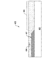
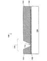
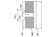
図4Aは、製造シーケンスの第1ステップで生成されうるアパーチャ層250(図3A)のための、1つのアパーチャ層構造400を示す。アパーチャ層構造400は、ガラス基板402上に単一の薄膜として蒸着された、アパーチャ層401を含む。アパーチャ層401は、アパーチャ層401内に一連のアパーチャ穴403を生成するためにエッチングされている。アパーチャ層401を、その上に製造される回路から絶縁するために、誘電体層404が、アパーチャ層401の上に蒸着されている。アパーチャ層401の、エッチングされた端は、上を覆う誘電体層404のひび割れの確率を減らすために、意図的に傾斜を付けられている。
Aperture Layer FIG. 4A shows one aperture layer structure 400 for the aperture layer 250 (FIG. 3A) that may be generated in the first step of the manufacturing sequence. The aperture layer structure 400 includes an aperture layer 401 deposited as a single thin film on a glass substrate 402. Aperture layer 401 has been etched to create a series of aperture holes 403 in aperture layer 401. A dielectric layer 404 is deposited over the aperture layer 401 to insulate the aperture layer 401 from the circuits fabricated thereon. The etched edge of the aperture layer 401 is intentionally beveled to reduce the probability of cracking of the overlying dielectric layer 404.

アパーチャ層401は、バックライトから見る人への光の通過を妨げるように設計される。遮光アパーチャ層として使用するための適切な材料としては、以下に限定されるものではないが、Al、Cr、Au、Ag、Cu、Ni、Ta、Ti、Nd、Nb、W、Moなどの金属、および/またはその合金が挙げられる。30nmを超える厚さに蒸着される場合、そのような材料は、光の透過を妨げるのに効果的である。蒸着は、蒸発(evaporation)、スパッタリング、または化学気相蒸着法によって達成されてもよい。   The aperture layer 401 is designed to prevent the passage of light from the backlight to the viewer. Suitable materials for use as the light blocking aperture layer include, but are not limited to, metals such as Al, Cr, Au, Ag, Cu, Ni, Ta, Ti, Nd, Nb, W, and Mo And / or alloys thereof. Such materials are effective in preventing light transmission when deposited to a thickness greater than 30 nm. Deposition may be achieved by evaporation, sputtering, or chemical vapor deposition.

多くの実装において、アパーチャ層401は、光を吸収する機能を有することが好ましい。ほとんどの金属膜は、光の一定の割合を吸収し、残りを反射する。一部の適用例では、ディスプレイのコントラストを向上するために、アパーチャ層401に当たる環境光の反射を回避することが望ましい。そのような適用例では、アパーチャ層401は、「ブラックマトリクス」と呼ばれてもよい。光の吸収において効果的な、すなわち、ブラックマトリクス内に使用するための、いくつかの金属合金としては、以下に限定されるものではないが、MoCr、MoW、MoTi、MoTa、TiW、およびTiCrが挙げられる。上記の合金から、またはNiおよびCrなどの単純金属から形成された、粗面を有する金属膜も、光の吸収において効果的な可能性がある。そのような膜は、高いガス圧力(20ミリトール(mtorr)を超えるスパッタ雰囲気)内でのスパッタ蒸着によって生成されてもよい。粗い金属膜は、さらに、液体スプレーまたはプラズマスプレーの適用による金属粒子の散布と、それに続く、熱シンタリングステップとによって形成されてもよい。誘電体層404などの、誘電体層が、次に、金属粒子の剥離または剥落を防止するために追加される。   In many implementations, the aperture layer 401 preferably has a function of absorbing light. Most metal films absorb a certain percentage of light and reflect the rest. In some applications, it is desirable to avoid reflection of ambient light striking the aperture layer 401 to improve display contrast. In such applications, the aperture layer 401 may be referred to as a “black matrix”. Some metal alloys that are effective in light absorption, i.e., for use in a black matrix include, but are not limited to, MoCr, MoW, MoTi, MoTa, TiW, and TiCr. Can be mentioned. A metal film having a rough surface formed from the above alloys or from simple metals such as Ni and Cr may also be effective in absorbing light. Such a film may be produced by sputter deposition in high gas pressure (sputter atmosphere above 20 mtorr). The rough metal film may further be formed by spreading metal particles by application of a liquid spray or plasma spray followed by a thermal sintering step. A dielectric layer, such as dielectric layer 404, is then added to prevent delamination or flaking of the metal particles.

アモルファスまたは多結晶のSi、Ge、CdTe、InGaAsなどの半導体材料、コロイド黒鉛(炭素)、ならびに、SiGeなどの合金も、光の吸収において効果的である。これらの材料は、薄膜を通したいかなる光の透過も防止するために、500nmを超える厚さを有する膜内に蒸着されてもよい。以下に限定されるものではないが、CuO、NiO、Cr、AgO、SnO、ZnO、TiO、Ta、MoO、CrN、TiN、またはTaNを含む、金属酸化物または窒化物も、光の吸収において効果的な場合がある。これらの酸化物または窒化物の吸収は、酸化物が非化学量論的なやり方−しばしば、スパッタリングまたは蒸発(evaporation)による−で調整または蒸着される場合、特に、蒸着プロセスによって格子内の酸素の不足がもたらされる場合に、向上する。半導体の場合と同様に、金属酸化物は、膜を通した光の透過を防止するために、500nmを超える厚さに蒸着されるべきである。 Amorphous or polycrystalline semiconductor materials such as Si, Ge, CdTe, InGaAs, colloidal graphite (carbon), and alloys such as SiGe are also effective in absorbing light. These materials may be deposited in a film having a thickness greater than 500 nm to prevent any light transmission through the thin film. Metal oxides or nitrides including, but not limited to, CuO, NiO, Cr 2 O 3 , AgO, SnO, ZnO, TiO, Ta 2 O 5 , MoO 3 , CrN, TiN, or TaN May also be effective in absorbing light. The absorption of these oxides or nitrides is particularly important when the oxide is tuned or deposited in a non-stoichiometric manner—often by sputtering or evaporation—especially by the deposition process. Improve when shortages are brought. As with the semiconductor, the metal oxide should be deposited to a thickness greater than 500 nm to prevent light transmission through the film.

サーメットと呼ばれる、材料群も、光の吸収において効果的である。サーメットは、通常、酸化物または窒化物の母体内に、小さな金属粒子が浮遊させられた、複合材料である。例としては、Cr母体内のCr粒子、またはSiO母体内のCr粒子が挙げられる。母体内で浮遊させられるその他の金属粒子は、Ni、Ti、Au、Ag、Mo、Nb、および炭素であってもよい。その他の母体材料としては、TiO、Ta、Al、およびSiが挙げられる。 A group of materials called cermets is also effective in absorbing light. Cermet is a composite material, usually with small metal particles suspended in an oxide or nitride matrix. Examples include Cr particles in the Cr 2 O 3 matrix or Cr particles in the SiO 2 matrix. Other metal particles suspended in the mother body may be Ni, Ti, Au, Ag, Mo, Nb, and carbon. Examples of other base materials include TiO 2 , Ta 2 O 5 , Al 2 O 3 , and Si 3 N 4 .

適切な薄膜材料間での光の相殺的干渉を利用して、多層吸収構造を作成することが可能である。代表的な実装としては、酸化物または窒化物の部分反射層(partially reflecting layer)を、適切な反射率の金属とともに使用することが挙げられる。酸化物は、例えば、CrO、TiO、Al、またはSiOなどの金属酸化物、あるいは、Siのような窒化物であってもよく、金属は、Cr、Mo、Al、Ta、Tiなどの適切な金属であってもよい。一実装では、基板から入る光の吸収のために、金属酸化物の、10〜500nmの範囲の薄層が、最初に、基板402の表面上に蒸着され、それに続いて、10〜500nmの厚さの金属層が蒸着される。別の実装では、基板と反対の方向から入る光の吸収のために、金属層が最初に蒸着され、続いて、金属酸化物が蒸着される。両方の場合に、2層スタックの吸収率は、酸化物層の厚さが、0.55ミクロンの4分の1を酸化物層の屈折率で割った値に実質的に等しいように選択される場合に、最適化されてもよい。 Multi-layer absorption structures can be created using destructive interference of light between suitable thin film materials. A typical implementation includes the use of an oxide or nitride partially reflecting layer with a metal of appropriate reflectivity. The oxide may be, for example, a metal oxide such as CrO 2 , TiO 2 , Al 2 O 3 , or SiO 2 , or a nitride such as Si 3 N 4 , and the metal may be Cr, Mo, Appropriate metals such as Al, Ta and Ti may be used. In one implementation, for absorption of light entering from the substrate, a thin layer of metal oxide in the range of 10-500 nm is first deposited on the surface of the substrate 402 followed by a thickness of 10-500 nm. A metal layer is deposited. In another implementation, a metal layer is deposited first, followed by a metal oxide, for absorption of light entering from the opposite direction to the substrate. In both cases, the absorptivity of the two-layer stack is selected so that the thickness of the oxide layer is substantially equal to a quarter of 0.55 microns divided by the refractive index of the oxide layer. May be optimized.

別の実装では、金属層が基板上に蒸着され、それに続いて、計算された厚さの適切な酸化物層が蒸着される。次に、薄い金属が部分反射のみを行うように、金属の薄層が、酸化物の上に蒸着される(0.02ミクロン未満の厚さ)。金属層からの部分反射は、基板金属層からの反射と相殺的に干渉し、それにより、ブラックマトリクス効果を発生させる。吸収は、酸化物層の厚さが、0.55ミクロンの4分の1を酸化物層の屈折率で割った値に実質的に等しいように選択される場合に、最大化される。   In another implementation, a metal layer is deposited on the substrate, followed by an appropriate oxide layer of the calculated thickness. Next, a thin layer of metal is deposited over the oxide (thickness less than 0.02 microns) so that the thin metal only performs partial reflection. Partial reflection from the metal layer interferes with the reflection from the substrate metal layer in a destructive manner, thereby generating a black matrix effect. Absorption is maximized when the thickness of the oxide layer is selected to be substantially equal to a quarter of 0.55 microns divided by the refractive index of the oxide layer.

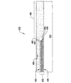
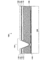
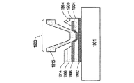
図4Bは、第2のアパーチャ層構造450の例示的実施形態である。第2のアパーチャ層構造450は、反射性である一方の側と、光吸収性であるもう一方の側とを有する、アパーチャ層452を含む。2005年9月2日出願の米国特許出願第11/218,690号明細書に記載されているように、アパーチャ層の1つの表面が、金属などの、反射性材料で作られている場合、アパーチャ層は、光学的効率を増加させるために、透過させられなかった光を再循環させて、取り付けられたバックライト内に戻す、鏡面として働いてもよい。そのような反射は、金属が蒸着される場合、スパッタリングを介してまたはイオンアシスト蒸着法(ion assisted evaporation)によって達成されるように、高密度で滑らかな薄膜を生成するような方法で強化されてもよい。強化された反射率を有する金属膜としては、Ag、Au、およびアルミニウムが挙げられる。   FIG. 4B is an exemplary embodiment of the second aperture layer structure 450. The second aperture layer structure 450 includes an aperture layer 452 having one side that is reflective and the other side that is light absorbing. If one surface of the aperture layer is made of a reflective material, such as metal, as described in US patent application Ser. No. 11 / 218,690 filed on Sep. 2, 2005, The aperture layer may act as a mirror that recycles light that has not been transmitted back into the attached backlight to increase optical efficiency. Such reflections are enhanced in such a way that when a metal is deposited, it produces a dense and smooth thin film, as achieved through sputtering or by ion assisted evaporation. Also good. Examples of metal films having enhanced reflectivity include Ag, Au, and aluminum.

アパーチャ層452は、基板453上に蒸着される複合構造から形成される。図4Bのアパーチャ層452は、アパーチャ層452の上面454上に当たる光を吸収し、アパーチャ層452の下部456に入射する光、すなわち、基板453を透過した後の光を、反射するように設計される。アパーチャ層452は、高屈折率層458と、低屈折率層460と、金属反射層462と、吸収層464という、4つの層を含む。アパーチャ層452は、アパーチャ穴466を形成するためにエッチングされ、誘電体層468で覆われる。異なる屈折率を有する屈折層458と460との結合によって、部分反射面(partially reflecting surfaces)の組がもたらされることを、当業者は認識するであろう。これらの部分反射面のうちの少なくとも2つの間の間隔を制御することによって、光学干渉により、膜スタックの反射率を強化することが可能である。多層膜は、広い波長帯域にわたって、または、例えば、バックライトから放射される波長に一致する波長などの、離散的な個別波長数において、高い反射率を提供するように設計されてもよい。   The aperture layer 452 is formed from a composite structure deposited on the substrate 453. The aperture layer 452 in FIG. 4B is designed to absorb light impinging on the upper surface 454 of the aperture layer 452 and to reflect light incident on the lower portion 456 of the aperture layer 452, ie, light that has passed through the substrate 453. The The aperture layer 452 includes four layers: a high refractive index layer 458, a low refractive index layer 460, a metal reflection layer 462, and an absorption layer 464. Aperture layer 452 is etched to form aperture hole 466 and covered with dielectric layer 468. Those skilled in the art will recognize that the combination of refractive layers 458 and 460 having different refractive indices provides a set of partially reflecting surfaces. By controlling the spacing between at least two of these partially reflective surfaces, it is possible to enhance the reflectivity of the film stack by optical interference. The multilayer film may be designed to provide high reflectivity over a wide wavelength band or at a discrete number of discrete wavelengths such as, for example, a wavelength that matches the wavelength emitted from the backlight.

高屈折率層458の候補となる薄膜としては、以下に限定されるものではないが、TiO、HfO、Ta、Nb、Cr、Sc、Bi、In、およびAlが挙げられる。低屈折率層460の候補となる薄膜としては、SiO、Si、MgF、CaF、およびHfF、ならびにダイヤモンド状炭素が挙げられる。これらの膜は、反応性スパッタリング、反応性蒸着法(reactive evaporation)、イオンアシスト蒸着法(ion−assisted evaporation)、イオンアシストイオンビームスパッタリング(ion−assisted ion beam sputtering)によって、または化学気相蒸着法によって、蒸着されてもよい。図4Bは、高屈折率層と低屈折率層との1つのペアのみを示している。これらの屈折層の複数のペアを順に蒸着することによって、反射率を向上することが可能であることを、当業者は理解するであろう。多くの場合、各屈折層(460および458)の厚さが、0.55ミクロンの4分の1を、層の屈折率によって割った値に実質的に等しいように選択された場合に、可視スペクトルに対する反射率は最大化されることが可能である。 The thin film that is a candidate for the high refractive index layer 458 is not limited to the following, but includes TiO 2 , HfO 2 , Ta 2 O 5 , Nb 2 O 5 , Cr 2 O 3 , Sc 2 O 3 , Bi. 2 O 3 , In 2 O 3 , and Al 2 O 3 . Examples of thin films that can be candidates for the low refractive index layer 460 include SiO 2 , Si 3 N 4 , MgF 2 , CaF 2 , and HfF 4 , and diamond-like carbon. These films are formed by reactive sputtering, reactive evaporation, ion-assisted evaporation, ion-assisted ion beam sputtering, or chemical vapor deposition. May be deposited. FIG. 4B shows only one pair of a high refractive index layer and a low refractive index layer. One skilled in the art will appreciate that the reflectivity can be improved by sequentially depositing multiple pairs of these refractive layers. Often visible when the thickness of each refractive layer (460 and 458) is chosen to be substantially equal to a quarter of 0.55 microns divided by the refractive index of the layer. The reflectivity for the spectrum can be maximized.

2つの屈折層458または460のうちのいずれか1つが、アパーチャ層456から除去されてもよく、それでもアパーチャ層452の反射率は、透明基板453の上に蒸着された単純な金属の反射率よりも実質的な程度まで向上する。金属層462と透明基板453との間に置かれる屈折層が、基板453の屈折率よりも小さな屈折率を有する限り、改良がもたらされてもよい。   Either one of the two refractive layers 458 or 460 may be removed from the aperture layer 456, yet the reflectivity of the aperture layer 452 is more than the reflectivity of a simple metal deposited on the transparent substrate 453. Is also improved to a substantial extent. Improvement may be provided as long as the refractive layer placed between the metal layer 462 and the transparent substrate 453 has a refractive index smaller than that of the substrate 453.

アパーチャ層452内の金属反射層462は、入射光を反射するだけでなく、光の透過を妨げるようにも働く。遮光アパーチャ層として使用するための、上に記載した金属膜および/または半導体材料のうちのいずれも、金属反射層のために利用されてもよい。   The metal reflection layer 462 in the aperture layer 452 not only reflects incident light but also acts to prevent light transmission. Any of the metal films and / or semiconductor materials described above for use as a light blocking aperture layer may be utilized for the metal reflective layer.

吸収層464は、基板453の側の反対の側から到着する光の反射を防止するように働く。ブラックマトリクスとともに使用するための、上に記載した吸収性材料のうちのいずれも、アパーチャ層452の一番上の層として使用されてもよい。   The absorbing layer 464 serves to prevent reflection of light arriving from the opposite side of the substrate 453 side. Any of the absorbent materials described above for use with a black matrix may be used as the top layer of the aperture layer 452.

アパーチャ穴466を形成するために必要とされるエッチングプロセスは、RFまたはDCプラズマエッチング、イオンスパッタリング、または湿式化学エッチングを含んでもよい。   The etching process required to form the aperture hole 466 may include RF or DC plasma etching, ion sputtering, or wet chemical etching.

アパーチャ層452の別の実装では、2層薄膜スタックが形成されてもよい。最初に、Ag、Au、またはAlなどの、高い反射率を有する金属膜が、表面上に蒸着される。次に、上に記載した吸収性ブラックマトリクス材料のうちの1つが、金属の上に蒸着される。   In another implementation of the aperture layer 452, a two-layer thin film stack may be formed. Initially, a highly reflective metal film, such as Ag, Au, or Al, is deposited on the surface. Next, one of the absorbent black matrix materials described above is deposited on the metal.

図4Bに示す複合アパーチャ層内の層の順序が逆にされて、吸収層が基板の隣に位置し、反射膜スタックが基板と反対の側を向くようにされることが好ましい実装が存在する。そのような実装は、図22に関して説明する。   There are implementations in which the order of the layers in the composite aperture layer shown in FIG. 4B is reversed so that the absorber layer is located next to the substrate and the reflective film stack faces away from the substrate. . Such an implementation is described with respect to FIG.

複合アパーチャ層452の製造のための好ましい実施形態は、次のように進められる。第1に、高屈折率層458のために、厚さ54nm±3nmのTiOの層が、Oの分圧内でのTiの反応性スパッタ蒸着によって蒸着される。次に、低屈折率層460のために、SiOの91nm±5nmの膜が、Oの分圧内でのSiOの反応性スパッタ蒸着によって蒸着される。次に、金属反射層462のために、滑らかなAlの100nm±5nmの膜が、高真空、非酸化環境内でのスパッタ蒸着によって蒸着される。次に、アパーチャ穴466を形成するために、3つの膜458、460、および462がパターニングされる。一般的なフォトレジストが、当業界で周知のように塗布され、次に、アパーチャ穴466のパターンを有するフォトマスクを通して紫外線露光される。フォトレジストは、次に、化学的に現像されて、エッチングマスクとなる。3つの膜のスタックのエッチングは、Arイオンを使用した、イオンビームミリングシステムを使用して実行され、それにより、それぞれの膜は順に除去されるが、フォトレジストはすべて除去されるわけではない。薄膜のエッチングが完了した後は、残りのフォトレジストが、水性または溶液型のいずれかのストリッパ化合物を使用して、あるいは、オゾンおよび/またはプラズマアッシングによって除去される。 A preferred embodiment for the fabrication of composite aperture layer 452 proceeds as follows. First, for the high refractive index layer 458, a layer of TiO 2 with a thickness of 54 nm ± 3 nm is deposited by reactive sputter deposition of Ti within the partial pressure of O 2 . Then, because of the low refractive index layer 460, film 91 nm ± 5 nm of SiO 2 is deposited by reactive sputter deposition of SiO 2 in minutes pressure internal of O 2. Next, a smooth 100 nm ± 5 nm film of Al is deposited for metal reflective layer 462 by sputter deposition in a high vacuum, non-oxidizing environment. Next, the three membranes 458, 460, and 462 are patterned to form aperture holes 466. A common photoresist is applied as is well known in the art and then UV exposed through a photomask having a pattern of aperture holes 466. The photoresist is then chemically developed to become an etching mask. Etching the stack of three films is performed using an ion beam milling system using Ar ions, which removes each film in turn, but not all of the photoresist. After the thin film etch is complete, the remaining photoresist is removed using either an aqueous or solution type stripper compound or by ozone and / or plasma ashing.

次に、吸収層464の第1の構成要素として、厚さ250nm±10nmのSiの薄膜が、プラズマアシスト化学気相蒸着法(plasma assisted chemical vapor deposition)によって蒸着される。次に、吸収層464の第2の構成要素として、厚さ500nm±40nmのアモルファスシリコンの層が、プラズマアシスト化学気相蒸着法(plasma assisted chemical vapor deposition)によって蒸着される。これらの膜は、次に、上記と同様のフォトレジスト露光および現像ステップを使用してアパーチャ穴466を形成するために、同様のフォトマスクを使用してパターニングされる。Siおよびアモルファスシリコンのエッチングが、次に、反応性イオンエッチングによって実行される。最後に、50nm±4nmのAlの膜が、原子層蒸着によって、一面に覆うやり方で蒸着される。 Next, a thin film of Si 3 N 4 having a thickness of 250 nm ± 10 nm is deposited as a first component of the absorption layer 464 by a plasma assisted chemical vapor deposition (plasma assisted chemical vapor deposition) method. Next, an amorphous silicon layer having a thickness of 500 nm ± 40 nm is deposited as a second constituent element of the absorption layer 464 by plasma assisted chemical vapor deposition (plasma assisted chemical vapor deposition). These films are then patterned using a similar photomask to form aperture holes 466 using the same photoresist exposure and development steps as described above. Etching of Si 3 N 4 and amorphous silicon is then performed by reactive ion etching. Finally, a film of 50 nm ± 4 nm of Al 2 O 3 is deposited in such a way that it covers one side by atomic layer deposition.

制御マトリクス
別の実装では、アパーチャ層は、上位層内の制御マトリクスへの独自の電気的接続を有する、制御マトリクスの電気的構成要素のうちの1つとして利用されてもよい。図5A〜図5Cは、そのような総合設計を示す。
Control Matrix In another implementation, the aperture layer may be utilized as one of the electrical components of the control matrix that has its own electrical connection to the control matrix in the upper layer. 5A-5C illustrate such an overall design.

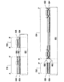
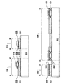
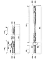
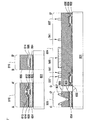
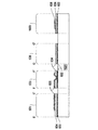
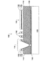
図5Aは、ピクセルのアレイをアドレス指定するための、ディスプレイ装置100内に含めるのに適した、別の制御マトリクス500の概略図である。制御マトリクス500は、デュアルアクチュエータシャッタ組立体504(すなわち、シャッタ開およびシャッタ閉の両方のアクチュエータを有するシャッタ組立体)を含むピクセル502のアレイを制御する。図5Bは、ピクセル502のアレイからの、2つの隣接するピクセル502の部分の平面図レイアウトである。図5Bのレイアウトは、基板上でのピクセル502のアレイの並行製造のために、制御マトリクス500の電気的構成要素がピクセル502内でどのように配置されてもよいかの一例を提供する。図5Cは、図5Bと同じであり、ピクセル502の追加の特徴を付記している。図5B/5Cなどのレイアウトは、ピクセル502の機能層のそれぞれのためのフォトマスクを生成するために利用されてもよい。制御マトリクス500の構成要素は一連の機能層から構築され、フォトマスクは、各層のための配列されたパターンを、基板505全体にわたってプリントするために使用される。アレイ502内のピクセルは、それぞれが実質的に正方形の形状であり、ピッチ、すなわち、ピクセル間の反復距離は、180〜200ミクロンの範囲内である。図5Cは、図6、図7、図8、および図10に関して説明する、さまざまな電気的および機械的構成要素の一連の層の断面図のための基準として使用される、断面マーカAA’〜GG’を示す。   FIG. 5A is a schematic diagram of another control matrix 500 suitable for inclusion within display device 100 for addressing an array of pixels. The control matrix 500 controls an array of pixels 502 that includes a dual actuator shutter assembly 504 (ie, a shutter assembly having both shutter open and shutter closed actuators). FIG. 5B is a plan view layout of two adjacent pixel 502 portions from an array of pixels 502. The layout of FIG. 5B provides an example of how the electrical components of the control matrix 500 may be arranged within the pixel 502 for parallel manufacturing of an array of pixels 502 on the substrate. FIG. 5C is the same as FIG. 5B and adds additional features of pixel 502. A layout such as FIGS. 5B / 5C may be utilized to generate a photomask for each of the functional layers of the pixel 502. The components of the control matrix 500 are constructed from a series of functional layers, and a photomask is used to print an arrayed pattern for each layer across the substrate 505. The pixels in the array 502 are each substantially square shaped and the pitch, i.e. the repeat distance between the pixels, is in the range of 180-200 microns. FIG. 5C is a cross-sectional marker AA′˜ used as a reference for a cross-sectional view of a series of layers of various electrical and mechanical components described with respect to FIGS. 6, 7, 8, and 10. GG 'is shown.

説明の目的のために、図5B/5Cでは、導体層と、半導体層と、シャッタ層のみを詳細に示す。誘電体層内に切り込まれるビア、またはアパーチャ層内にパターニングされる穴などの、その他のパターニングされる特徴の位置は、記号の表示および/または点線によって示される。   For illustrative purposes, FIGS. 5B / 5C show only the conductor layer, the semiconductor layer, and the shutter layer in detail. The location of other patterned features, such as vias cut into the dielectric layer, or holes patterned into the aperture layer, are indicated by symbolic representations and / or dotted lines.

図5Aおよび図5Bを参照すると、制御マトリクス500は、制御マトリクス500内のピクセル502の各行について、走査ライン相互接続506を含む。制御マトリクス500は、さらに、制御マトリクス500内のピクセル502の各列について、1つのデータ開相互接続508aおよび1つのデータ閉相互接続508bという、2つのデータ相互接続を含む。制御マトリクス500は、さらに、事前充電相互接続510と、大域的作動相互接続514と、シャッタ共通相互接続515とを含む。これらの相互接続510、514、および515は、アレイ内の複数行および複数列内のピクセル502間で共有される。一実装(以下でより詳細に説明する実装)においては、相互接続510、514、および515は、制御マトリクス500内のすべてのピクセル502間で共有される。   With reference to FIGS. 5A and 5B, the control matrix 500 includes a scan line interconnect 506 for each row of pixels 502 in the control matrix 500. The control matrix 500 further includes two data interconnects, one data open interconnect 508a and one data close interconnect 508b for each column of pixels 502 in the control matrix 500. The control matrix 500 further includes a precharge interconnect 510, a global actuation interconnect 514, and a shutter common interconnect 515. These interconnects 510, 514, and 515 are shared between pixels 502 in multiple rows and multiple columns in the array. In one implementation (the implementation described in more detail below), the interconnects 510, 514, and 515 are shared among all the pixels 502 in the control matrix 500.

制御マトリクス内の各ピクセル502は、シャッタ開充電トランジスタ516と、シャッタ開放電トランジスタ518と、シャッタ開書き込み許可トランジスタ517と、データ蓄積キャパシタ519とを含む。制御マトリクス500内の各ピクセル502は、さらに、シャッタ閉充電トランジスタ520と、シャッタ閉放電トランジスタ522と、シャッタ閉書き込み許可トランジスタ527と、データ蓄積キャパシタ529とを含む。   Each pixel 502 in the control matrix includes a shutter open charge transistor 516, a shutter open discharge transistor 518, a shutter open write enable transistor 517, and a data storage capacitor 519. Each pixel 502 in the control matrix 500 further includes a shutter closing charge transistor 520, a shutter closing discharge transistor 522, a shutter closing write permission transistor 527, and a data storage capacitor 529.

制御マトリクス内の各ピクセル502は、さまざまなビア構造を含み、それらは、図5B/5C内の対角線を有するボックスの記号によって示されている。制御マトリクス500は、いくつかのM1−M2ビア531(すなわち、第1の金属層M1を第2の金属層M2に接続するビア)と、Ap−M1ビア533(すなわち、アパーチャ層547を第1の金属層M1に接続するビア)と、2つの駆動アンカー535と、4つのコンプライアント駆動ビーム537と、4つのシャッタアンカー539と、4つのコンプライアントロードビーム541と、アパーチャ穴543と、シャッタ545とを含む。アパーチャ穴543は、点線によって示されている。   Each pixel 502 in the control matrix includes various via structures, which are indicated by the diagonal box symbols in FIGS. 5B / 5C. The control matrix 500 includes a number of M1-M2 vias 531 (ie, vias that connect the first metal layer M1 to the second metal layer M2) and Ap-M1 vias 533 (ie, the aperture layer 547 as the first). ), Two drive anchors 535, four compliant drive beams 537, four shutter anchors 539, four compliant load beams 541, aperture holes 543, and shutters 545. Including. The aperture hole 543 is indicated by a dotted line.

2つの隣接するピクセル502の部分が、図5Bおよび図5Cに示されている。各ピクセル502について、シャッタ545は、左に移動することによって、アパーチャ穴543を覆い隠す。トランジスタ516、517、および518を含む、各ピクセルのシャッタ開作動電子回路は、各シャッタ組立体504のすぐ右に配置される(2つのピクセルは同等であるが、シャッタ開電子回路は、図5B/5C内では、最も左のシャッタ組立体504についてのみ含まれている)。トランジスタ520、522、および527を含む、各ピクセルのシャッタ閉電子回路は、各シャッタ組立体のすぐ左に配置される(再び、ピクセル502は同等であるが、シャッタ閉電子回路は、最も右のシャッタ組立体504についてのみ示されている)。   The portions of two adjacent pixels 502 are shown in FIGS. 5B and 5C. For each pixel 502, the shutter 545 covers the aperture hole 543 by moving to the left. The shutter opening actuation electronics for each pixel, including transistors 516, 517, and 518, are located immediately to the right of each shutter assembly 504 (two pixels are equivalent, but the shutter opening electronics are shown in FIG. 5B). Within / 5C, only the leftmost shutter assembly 504 is included). The shutter close electronics for each pixel, including transistors 520, 522, and 527, is located immediately to the left of each shutter assembly (again, pixel 502 is equivalent, but the shutter close electronics is the rightmost Only shown for shutter assembly 504).

所与のピクセル502について、コンプライアントロードビーム541は、シャッタ545を、4つのシャッタアンカー539に機械的に接続し、シャッタ545を、基板表面の上で浮遊させる。ロードビーム541の隣に配置される、コンプライアント駆動ビーム537は、駆動アンカー535に機械的に接続される。(シャッタ545の右に配置された)一方の組の駆動ビーム537は、駆動アンカーに機械的に接続され、そして、駆動アンカー535とM1−M2ビア531との両方によって、シャッタ開充電トランジスタ516のドレインに電気的に接続される。シャッタ545の右側にある駆動ビーム537とロードビーム541との間に、最小作動電圧よりも大きな電圧を印加することによって、シャッタ545は、開位置に、すなわちアパーチャ穴543から離れるように、移動させられてもよい。シャッタの右にある駆動ビーム537およびロードビーム541の組は、合わせて、シャッタ開アクチュエータを形成する。(各シャッタ545の左に配置された)もう一方の組の駆動ビーム537は、駆動アンカー535に機械的に接続され、そして、駆動アンカー535とM1−M2ビア531との両方によって、シャッタ閉充電トランジスタ520のドレインに電気的に接続される。シャッタ545の左側にある駆動ビーム537とロードビーム541との間に、最小作動電圧よりも大きな電圧をもたらすことによって、シャッタ545は、(図5B/5Cに示すような)閉位置に、すなわちアパーチャ穴543の上の位置に、移動させられてもよい。シャッタ545の左にある駆動ビーム537およびロードビーム541の組は、シャッタ閉アクチュエータを形成する。   For a given pixel 502, a compliant load beam 541 mechanically connects the shutter 545 to four shutter anchors 539, causing the shutter 545 to float above the substrate surface. A compliant drive beam 537, located next to the load beam 541, is mechanically connected to the drive anchor 535. One set of drive beams 537 (located to the right of the shutter 545) is mechanically connected to the drive anchor, and by both the drive anchor 535 and the M1-M2 via 531 the shutter open charge transistor 516 Electrically connected to the drain. By applying a voltage greater than the minimum operating voltage between the drive beam 537 on the right side of the shutter 545 and the load beam 541, the shutter 545 is moved to the open position, that is, away from the aperture hole 543. May be. The set of drive beam 537 and load beam 541 to the right of the shutter together form a shutter opening actuator. The other set of drive beams 537 (located to the left of each shutter 545) is mechanically connected to the drive anchor 535 and is shutter closed charged by both the drive anchor 535 and the M1-M2 via 531. It is electrically connected to the drain of the transistor 520. By providing a voltage greater than the minimum operating voltage between the drive beam 537 and the load beam 541 on the left side of the shutter 545, the shutter 545 is in the closed position (as shown in FIGS. 5B / 5C), i.e. the aperture. It may be moved to a position above the hole 543. The combination of the drive beam 537 and the load beam 541 on the left of the shutter 545 forms a shutter closing actuator.

実施の際、制御マトリクス500は、a)アクチュエータの事前充電、b)ピクセルアドレス指定およびデータ蓄積、ならびにc)ピクセルの大域的作動という、別個の電気的機能を、独立に制御するために設計される。   In implementation, the control matrix 500 is designed to independently control separate electrical functions: a) actuator precharging, b) pixel addressing and data storage, and c) global operation of the pixels. The

各フレームアドレス指定サイクルの最初に、制御マトリクス500は、事前充電相互接続510に電圧を印加する。事前充電相互接続510はシャッタ開およびシャッタ閉充電トランジスタ516および520のゲートとドレインとの両方に接続されているため、この電圧の印加は、これらのトランジスタ516および520の両方をオンにするように働く。事前充電相互接続510は、シャッタ545の作動のために必要とされる最小値を超える電圧まで、例えば、15ボルトを超える電圧まで、または、一部の実施形態では、30ボルトを超える電圧まで、パルス印加される。シャッタ開およびシャッタ閉アクチュエータのそれぞれのアクチュエータが充電された後は、事前充電相互接続510上の電圧は0に戻され、シャッタ開およびシャッタ閉トランジスタ516および520の両方は、次に、それらのオフ状態に戻る。シャッタ開およびシャッタ閉アクチュエータのそれぞれに提供された電荷は、それぞれのアクチュエータ上に蓄積されたままになり、その理由は、これらのアクチュエータに給電するトランジスタが、それらのオフ状態に戻っているからである。   At the beginning of each frame addressing cycle, the control matrix 500 applies a voltage to the precharge interconnect 510. Since the precharge interconnect 510 is connected to both the gate and drain of the shutter open and shutter close charge transistors 516 and 520, application of this voltage will cause both transistors 516 and 520 to turn on. work. The precharge interconnect 510 may be up to a voltage exceeding the minimum required for operation of the shutter 545, for example, to a voltage exceeding 15 volts, or in some embodiments to a voltage exceeding 30 volts. A pulse is applied. After each actuator of the shutter open and shutter close actuators is charged, the voltage on the precharge interconnect 510 is returned to zero, and both shutter open and shutter close transistors 516 and 520 are then turned off. Return to state. The charge provided to each of the shutter-open and shutter-close actuators remains stored on the respective actuator because the transistors that power these actuators have returned to their off state. is there.

各行は、次に、走査ライン相互接続506上に書き込み許可電圧Vweを配置することによって、順に書き込み許可される。ピクセル502の特定の行が書き込み許可されている間、制御マトリクス500は、データ電圧を、制御マトリクス500内のピクセル502の各列に対応したデータ開相互接続508aまたはデータ閉相互接続508bのいずれかに印加する。書き込み許可される行についての走査ライン相互接続506へのVweの印加により、対応する走査ライン内のピクセル502の書き込み許可トランジスタ517および527の両方がオンになる。データ相互接続508aおよび508bに印加される電圧は、それにより、それぞれのピクセル502のデータ蓄積キャパシタ519および529上に蓄積されることが可能となる。一般に、正しい作動を確実にするために、データ電圧は、シャッタ組立体504につき1つの蓄積キャパシタ519または529のみに蓄積されることが許可される。 Each row, then by placing a write enable voltage V we on scan-line interconnect 506, are sequentially write permission. While a particular row of pixels 502 is allowed to be written, the control matrix 500 applies the data voltage to either the data open interconnect 508a or the data close interconnect 508b corresponding to each column of pixels 502 in the control matrix 500. Apply to. The application of V we to the scan-line interconnect 506 of the row to be write-enabled, both of the write-enable transistor 517 and 527 of pixels 502 in the corresponding scan line is turned on. The voltages applied to the data interconnects 508a and 508b can thereby be stored on the data storage capacitors 519 and 529 of the respective pixels 502. In general, data voltages are allowed to be stored in only one storage capacitor 519 or 529 per shutter assembly 504 to ensure proper operation.

制御マトリクス500においては、大域的作動相互接続514は、シャッタ開放電スイッチトランジスタ518およびシャッタ閉放電トランジスタ522の両方のソースに接続される。大域的作動相互接続514を、シャッタ共通相互接続515の電位よりも大幅に上の電位に維持することにより、キャパシタ519および529上にどれだけの電荷が蓄積されているかにかかわらず、放電スイッチトランジスタ518または522のうちのいずれもオンになることが防止される。制御マトリクス500における大域的作動は、大域的作動相互接続514を、シャッタ共通相互接続515の電位以下の電位にして、放電スイッチトランジスタ518または522が、いずれかのキャパシタ519または520上にデータ電圧が蓄積されているかどうかに従ってオンになることを可能にすることによって達成される。オン状態に切り換えられた場合、シャッタ開放電スイッチトランジスタ518またはシャッタ閉放電トランジスタ522は、それらのそれぞれのアクチュエータの一方または他方から電荷が流出することを許可する。例えば、シャッタ開放電トランジスタ518のみをオンにすることによって、シャッタ545の右の駆動ビーム537上に蓄積された電荷は、駆動アンカー535、M1−M2ビア531を通し、トランジスタ518を通して、そして、大域的作動相互接続514を通して流れ出る。結果として、最小作動電圧を超える電圧が、シャッタと、シャッタの左の駆動ビームとの間のみに残り、シャッタは左に、そして開位置に移動させられる。   In control matrix 500, global actuation interconnect 514 is connected to the sources of both shutter open discharge switch transistor 518 and shutter closed discharge transistor 522. By maintaining the global actuation interconnect 514 at a potential significantly above the potential of the shutter common interconnect 515, no matter how much charge is stored on the capacitors 519 and 529, the discharge switch transistor Either 518 or 522 is prevented from being turned on. Global operation in the control matrix 500 causes the global operation interconnect 514 to be less than or equal to the potential of the shutter common interconnect 515 so that the discharge switch transistor 518 or 522 has a data voltage on either capacitor 519 or 520. This is accomplished by allowing it to turn on according to whether it has been accumulated. When switched to the on state, the shutter open discharge switch transistor 518 or the shutter closed discharge transistor 522 allows charge to flow out of one or the other of their respective actuators. For example, by turning on only the shutter open discharge transistor 518, the charge accumulated on the right drive beam 537 of the shutter 545 passes through the drive anchor 535, the M1-M2 via 531, through the transistor 518, and globally. Out through the statically actuated interconnect 514. As a result, a voltage exceeding the minimum operating voltage remains only between the shutter and the left drive beam of the shutter, and the shutter is moved to the left and to the open position.

データ蓄積キャパシタ519および521に部分的電圧を印加することにより、大域的作動相互接続514がその作動電位にされている時間中に、放電スイッチトランジスタ518および522の部分的オンが可能となる。これにより、シャッタ組立体504上でアナログ電圧が作られて、アナロググレースケールを提供することが可能となる。   By applying a partial voltage to data storage capacitors 519 and 521, discharge switch transistors 518 and 522 can be partially turned on during the time that global actuation interconnect 514 is at its actuation potential. This allows an analog voltage to be created on the shutter assembly 504 to provide an analog gray scale.

図5B/5Cに示すレイアウトは、2つの隣接するピクセルの部分を含み、その間で、相互接続のいくつかは単独で割り当てられ、相互接続のいくつかは共通に共有される。これらのピクセルのそれぞれは、制御マトリクス500の1つの列に沿ったすべてのピクセル502を垂直に接続する、1つのデータ開相互接続508aと1つのデータ閉相互接続508bとを含む。図5B/5C内の2つの隣接するピクセル502は、さらに、制御マトリクス500の1つの行に沿ったすべてのピクセル502を水平に接続する、共通走査ライン相互接続506を共有する。2つの隣接するピクセルは、ただし、事前充電相互接続510と、大域的作動相互接続514とを、それらの間で共有する。列方向に沿って向けられた、これらの2つの相互接続は、2つのピクセル502のそれぞれの間に配置され、M1−M2ビア531を介した電気的接続を使用して、右と左の両方のピクセルに電圧信号を供給する。ディスプレイの周辺部(図示せず)において、複数の列からの事前充電相互接続ライン510および大域的作動相互接続ライン514は、それぞれ、他の事前充電相互接続ラインおよび他の大域的作動相互接続ラインに、さらに接続される。   The layout shown in FIGS. 5B / 5C includes two adjacent pixel portions, between which some of the interconnects are assigned independently and some of the interconnects are commonly shared. Each of these pixels includes one data open interconnect 508a and one data close interconnect 508b that vertically connects all the pixels 502 along one column of the control matrix 500. Two adjacent pixels 502 in FIGS. 5B / 5C also share a common scan line interconnect 506 that horizontally connects all the pixels 502 along one row of the control matrix 500. Two adjacent pixels, however, share a precharge interconnect 510 and a global actuation interconnect 514 between them. These two interconnects, oriented along the column direction, are placed between each of the two pixels 502, using electrical connections through M1-M2 vias 531, both right and left A voltage signal is supplied to the pixels. In the periphery of the display (not shown), the precharge interconnect line 510 and the global actuation interconnect line 514 from multiple columns are respectively the other precharge interconnect lines and other global actuation interconnect lines. Are further connected.

制御マトリクス500は、シャッタ共通相互接続515を含み、シャッタ共通相互接続515は、図5B/5Cのレイアウト内では、アパーチャ層547と呼ばれる独立した導体層によって構築される。アパーチャ層547は、図3Aおよび図3Bに示したように、制御マトリクス500の他のすべての層の下にある別個の層として製造される。好ましい実施形態では、アパーチャ層547は、導電性材料から製造される。アパーチャ層のパターニングされた外形は、アパーチャ穴543の位置を除き、図5B/5Cには示されていない。制御マトリクス500内で、アパーチャ層は、すべての行およびすべての列内のすべてのシャッタ545間の共通の電気的接続を、シャッタアンカー539を使って行うために使用される。   The control matrix 500 includes a shutter common interconnect 515, which is constructed by an independent conductor layer called an aperture layer 547 in the layout of FIGS. 5B / 5C. Aperture layer 547 is fabricated as a separate layer below all other layers of control matrix 500, as shown in FIGS. 3A and 3B. In a preferred embodiment, the aperture layer 547 is made from a conductive material. The patterned outline of the aperture layer is not shown in FIGS. 5B / 5C, except for the position of the aperture hole 543. Within the control matrix 500, the aperture layer is used to make a common electrical connection with all the shutters 545 in all rows and all columns using the shutter anchor 539.

代替のレイアウト
図5B/5Cは、制御マトリクス500の構築のための適切なレイアウトの一例にすぎないということが理解されるべきである。多くのその他の均等なレイアウトが可能である。例えば、共通相互接続510および514は、図5B/5Cでは列方向に沿って通されているが、これらの相互接続が行方向に沿って通される他の実施形態が可能である。図5B/5Cでは、共通相互接続510および514は、トランジスタ518などの、トランジスタへのソースおよびドレイン接続と同じ金属レベルにおいて構築および/またはパターニングされる。ただし、これらの共通相互接続510および514が、薄膜トランジスタのゲートレベルにおいて構築される、他の実施形態が可能であり、また、これらの相互接続が、下にある導電性アパーチャ層547内に配置された、独立した電気的コネクタとしてパターニングされてもよい、さらに他の実施形態も可能である。
Alternative Layouts It should be understood that FIGS. 5B / 5C are only one example of a suitable layout for the construction of the control matrix 500. Many other equal layouts are possible. For example, common interconnects 510 and 514 are threaded along the column direction in FIGS. 5B / 5C, but other embodiments are possible where these interconnects are threaded along the row direction. In FIGS. 5B / 5C, common interconnects 510 and 514 are constructed and / or patterned at the same metal level as the source and drain connections to a transistor, such as transistor 518. However, other embodiments are possible where these common interconnects 510 and 514 are built at the gate level of the thin film transistor, and these interconnects are disposed within the underlying conductive aperture layer 547. Still other embodiments are possible that may be patterned as separate electrical connectors.

図5B/5Cに示す制御マトリクス500のレイアウトでは、シャッタ組立体504は、シャッタ545が、走査ライン相互接続506と平行な方向に移動するように並べられている。シャッタ545が、データ相互接続508aおよび508bと平行に移動する、他の実施形態が可能である。トランジスタ518またはキャパシタ519などの、電気的構成要素が、シャッタ組立体504の左または右だけでなく、上または下にも配置される実施形態も可能である。図5B/5Cでは、電気的構成要素は、ピクセル502内の異なる領域を占める。ただし、トランジスタ518またはキャパシタ519などの構成要素が、シャッタ組立体504の下にある他の薄膜層上に構築される、他の実施形態が可能である。   In the control matrix 500 layout shown in FIGS. 5B / 5C, the shutter assemblies 504 are arranged such that the shutters 545 move in a direction parallel to the scan line interconnect 506. Other embodiments are possible where the shutter 545 moves in parallel with the data interconnects 508a and 508b. Embodiments are possible where electrical components, such as transistor 518 or capacitor 519, are located not only on the left or right of shutter assembly 504, but also above or below. In FIGS. 5B / 5C, the electrical components occupy different areas within pixel 502. However, other embodiments are possible in which components such as transistor 518 or capacitor 519 are built on other thin film layers under shutter assembly 504.

当業界で周知の、多くの異なる薄膜スイッチが、制御マトリクス500の動作のために利用されてもよい。図6は、いくつかの適切なスイッチ構造のうちの1つの断面を示す。図6に示す構造は、シャッタ開放電トランジスタ518などの、トランジスタの断面を含む。トランジスタ518の構造は、アクティブマトリクス液晶ディスプレイのために当業界で使用されるものに類似している。図6の構造600は、さらに、液晶ディスプレイ内のピクセルキャパシタに接続するために一般に使用されるような、または、ディスプレイの周辺部でドライバ回路に接続するために一般に使用されるような、電極相互接続601を含む。トランジスタ518は、特に、反転スタガバックチャネルエッチング薄膜トランジスタ(inverted staggered back−channel−etched thin film transistor)として当業界で周知の構造を表す。この特定のトランジスタおよびその他の、形成および機能の説明は、Willem den Boer著、Active Matrix Liquid Crystal Displays(Elsevier,Amsterdam,2005)などの文献に見出すことができる。   Many different thin film switches, well known in the art, may be utilized for the operation of the control matrix 500. FIG. 6 shows a cross section of one of several suitable switch structures. The structure shown in FIG. 6 includes a cross section of a transistor, such as a shutter open discharge transistor 518. The structure of transistor 518 is similar to that used in the industry for active matrix liquid crystal displays. The structure 600 of FIG. 6 is further interdigitated, such as commonly used to connect to pixel capacitors in a liquid crystal display, or commonly used to connect to driver circuitry at the periphery of the display. Connection 601 is included. Transistor 518 represents a structure well known in the art, particularly as an inverted staggered back-channel-etched thin film transistor. A description of this particular transistor and other formations and functions can be found in literature such as by Willem den Boer, Active Matrix Liquid Crystal Displays (Elsevier, Amsterdam, 2005).

トランジスタ518は、薄膜または層の独特の組から構築され、その製造プロセスは、図7〜図10に関してより詳細に説明する。特に、トランジスタ518は、アパーチャ層602の上に配置される。アパーチャ層の上には、第1の誘電体層604が配置される。トランジスタ518の要素は、第1の導体層606と、第2の誘電体層608と、第1の半導体層610と、第2の導体層612と、第3の誘電体層614と、第3の導体層616とを含む。第1の導体層は、当業界では、ゲート金属層とも呼ばれ、トランジスタ518は、ボトムゲートトランジスタと呼ばれる。第2の導体層は、当業界では、トランジスタ518のソースおよびドレインへのコネクタとも呼ばれる。さらに、第3の導体層は、当業界では、電極または接点金属とも呼ばれる。   Transistor 518 is constructed from a unique set of thin films or layers, the fabrication process of which will be described in more detail with respect to FIGS. In particular, the transistor 518 is disposed on the aperture layer 602. A first dielectric layer 604 is disposed on the aperture layer. The elements of the transistor 518 include a first conductor layer 606, a second dielectric layer 608, a first semiconductor layer 610, a second conductor layer 612, a third dielectric layer 614, and a third Conductor layer 616. The first conductor layer is also referred to in the art as a gate metal layer, and transistor 518 is referred to as a bottom gate transistor. The second conductor layer is also referred to in the art as a connector to the source and drain of transistor 518. Further, the third conductor layer is also referred to in the art as an electrode or contact metal.

半導体層610は、一般に、アモルファスまたは多結晶シリコンから形成される。アモルファスシリコンは、プラズマ促進化学気相蒸着法(plasma enhanced chemical vapor deposition)(PECVD)によって、またはホットワイヤ蒸着によって、SiHなどの前駆体ガスから蒸着されてもよい。層610において使用されてもよいその他の半導体材料としては、ダイヤモンド状炭素、Si、Ge、GaAs、CdTe、またはその合金が挙げられる。半導体層の形成のための、その他の技術としては、低圧化学気相蒸着法およびスパッタリングが挙げられる。 The semiconductor layer 610 is generally formed from amorphous or polycrystalline silicon. Amorphous silicon may be deposited from a precursor gas such as SiH 4 by plasma enhanced chemical vapor deposition (PECVD) or by hot wire deposition. Other semiconductor materials that may be used in layer 610 include diamond-like carbon, Si, Ge, GaAs, CdTe, or alloys thereof. Other techniques for forming the semiconductor layer include low pressure chemical vapor deposition and sputtering.

半導体層610の上面には、アモルファスシリコンの導電率を増加するため、およびアモルファスシリコンと第2の導体層612との間のオーム接触を提供するために、不純物がドープされる。アモルファスまたは多結晶シリコンのいずれかとともに一般に使用される、導電性向上ドーパントとしては、リン、ヒ素、ホウ素、またはアルミニウムが挙げられる。これらのドーパントは、蒸着ステップの一部として、すなわち、PECVDチャンバ内でドーパント前駆体をSiHと混合することによって含まれてもよく、あるいは、ドーパントガスからの拡散によって、またはイオン打ち込みによって、後で追加されてもよい。 The top surface of the semiconductor layer 610 is doped with impurities to increase the conductivity of the amorphous silicon and to provide an ohmic contact between the amorphous silicon and the second conductor layer 612. Conductivity enhancing dopants commonly used with either amorphous or polycrystalline silicon include phosphorus, arsenic, boron, or aluminum. These dopants may be included as part of the deposition step, ie by mixing the dopant precursor with SiH 4 in a PECVD chamber, or by diffusion from the dopant gas or by ion implantation. May be added.

図6に示す代表的トランジスタ518などの、薄膜スイッチは、蒸着、マスキング、およびエッチングステップのシーケンスから製造される。トランジスタ518などの薄膜スイッチの形成に必要とされる、マスクおよび/または蒸着ステップの数は、3〜10の間で変化してもよい。同時に、薄膜スイッチを形成するために使用される、蒸着、パターニング、およびエッチングステップは、さらに、ピクセル間のアレイ相互接続、またはキャパシタなどの、薄膜構成要素を形成するために、あるいは、ディスプレイの周辺部における、ドライバチップへの電極接点を形成するためにも使用される。同様の、および/または追加の処理ステップが、MEMSシャッタディスプレイ内で有用な薄膜構成要素を形成するように、例えば、薄膜スイッチと、アパーチャ層602などのアパーチャ層との間の電気的接続を形成するように、あるいは、スイッチと、アレイ相互接続と、シャッタ組立体202またはシャッタ組立体504などの、シャッタ組立体との間の電気的接続を形成するように、適合されてもよい。   A thin film switch, such as the exemplary transistor 518 shown in FIG. 6, is fabricated from a sequence of deposition, masking, and etching steps. The number of masks and / or deposition steps required to form a thin film switch such as transistor 518 may vary between 3-10. At the same time, the deposition, patterning, and etching steps used to form the thin film switch can also be used to form thin film components, such as array interconnections between pixels, or capacitors, or the periphery of the display. It is also used to form electrode contacts to the driver chip in the part. Similar and / or additional processing steps form an electrical connection between, for example, a thin film switch and an aperture layer, such as aperture layer 602, to form a useful thin film component in a MEMS shutter display. Or may be adapted to form an electrical connection between a switch, an array interconnect, and a shutter assembly, such as shutter assembly 202 or shutter assembly 504.

製造手順700
図7は、制御マトリクスおよび関連するシャッタ組立体の構築のための、製造プロセスまたは手順700の一例を示す。図7の手順700は、アパーチャ層250またはアパーチャ層602などの、アパーチャ層の形成のためのステップを含む。手順700は、さらに、トランジスタ210またはトランジスタ518などの、スイッチまたはトランジスタの形成のためのステップを含む。手順700は、さらに、シャッタ組立体202またはシャッタ組立体504などの、シャッタ組立体の製造のためのステップを含む。図7の手順700は、トランジスタ518などの、反転、スタガ、バックチャネルエッチングトランジスタ(inverted, staggered, back−channel etched transistor)の形成に関して以下に記載される。プロセスの単純化のために、または、代替の薄膜スイッチおよび制御マトリクスの形成のために適切であってもよい、手順700の修正形態または代替方法は、図9に関して後述する。
Manufacturing procedure 700
FIG. 7 shows an example of a manufacturing process or procedure 700 for the construction of a control matrix and associated shutter assembly. The procedure 700 of FIG. 7 includes steps for the formation of an aperture layer, such as aperture layer 250 or aperture layer 602. Procedure 700 further includes steps for forming a switch or transistor, such as transistor 210 or transistor 518. Procedure 700 further includes steps for manufacturing a shutter assembly, such as shutter assembly 202 or shutter assembly 504. The procedure 700 of FIG. 7 is described below with respect to forming an inverted, staggered, back-channel etched transistor (such as transistor 518). A modification or alternative method of procedure 700, which may be appropriate for process simplification or for the formation of alternative thin film switches and control matrices, is described below with respect to FIG.

手順700は、ステップ705における、基板上のアパーチャ層602の形成で開始される。アパーチャ層の形成705は、ガラスまたはプラスチックであってもよい基板のクリーニングと、それに続く、アパーチャ層602の蒸着およびエッチングとを含む。ステップ705のいくつかの実装を、図4Aおよび図4Bに関してすでに説明した。場合によっては、アパーチャ層は、アパーチャ層452などの複合アパーチャ層であってもよい。   Procedure 700 begins with the formation of aperture layer 602 on the substrate in step 705. Aperture layer formation 705 includes cleaning the substrate, which may be glass or plastic, followed by deposition and etching of the aperture layer 602. Several implementations of step 705 have already been described with respect to FIGS. 4A and 4B. In some cases, the aperture layer may be a composite aperture layer, such as aperture layer 452.

手順700は、ステップ710における、誘電体層604などの、第1の誘電体層の蒸着およびエッチングに継続される。適切な誘電体材料としては、以下に限定されるものではないが、SiO、Si、Al、TiO、HfO、およびTaが挙げられ、それらは、スパッタリング、蒸発(evaporation)、または化学気相蒸着法のいずれかによって、おおよそ0.1〜2.0ミクロンの厚さに蒸着されてもよい。一般的なフォトレジストが、当業界で周知のように塗布され、次に、図5などのレイアウトに示されているような、フォトマスクパターンを通して紫外線露光され、最後に現像されて、エッチングマスクとされる。誘電体層604のエッチングが完了した後は、残りのフォトレジストが、水性または溶液型のいずれかのストリッパ化合物を使用して、あるいは、オゾンおよび/またはプラズマアッシングによって、除去される。第1の誘電体層604をパターニングするために使用されてもよいエッチングプロセスとしては、RFまたはDCプラズマエッチング、スパッタエッチング、または湿式化学エッチングが挙げられる。 Procedure 700 continues with the deposition and etching of a first dielectric layer, such as dielectric layer 604, at step 710. Suitable dielectric materials include, but are not limited to, SiO 2, Si 3 N 4 , Al 2 O 3, TiO 2, HfO 2, and Ta 2 O 5 and the like, they, sputtering It may be deposited to a thickness of approximately 0.1 to 2.0 microns, either by evaporation, or chemical vapor deposition. A common photoresist is applied as is well known in the art, then exposed to UV light through a photomask pattern, finally developed, as shown in the layout of FIG. Is done. After the etching of dielectric layer 604 is complete, the remaining photoresist is removed using either an aqueous or solution type stripper compound or by ozone and / or plasma ashing. Etching processes that may be used to pattern the first dielectric layer 604 include RF or DC plasma etching, sputter etching, or wet chemical etching.

手順700は、ステップ715における、導体層606などの、第1の導体層の蒸着およびエッチングに継続される。適切な導体材料としては、以下に限定されるものではないが、Al、Cu、Ag、Ni、Cr、Mo、W、Ti、Ta、Nd、Nb、およびその合金または組み合わせが挙げられる。当業界で使用されるいくつかの一般的な合金としては、TiW、MoW、MoCr、AlNd、AlTa、およびAlCrが挙げられる。2層金属も、第1の導体層606としての適用のために有用である。有用ないくつかの2層金属としては、Al上のCr、Al上のTa、Ag上のTa、Al上のTi、またはAl上のMoが挙げられる。Cr/Al/Cr、Cr/Al/Ti、Ti/Al/Ti、Cr/Al/Ta、またはCr/Ag/Taなどの、3層金属構成も、当業界で周知である。これらの金属または金属の組み合わせは、DCまたはRFスパッタリング、蒸発(evaporation)によって、または場合によっては、化学気相蒸着法によって適用されてもよい。適切な厚さは、0.1〜1.0ミクロンの範囲内であってもよい。第1の導体層606のパターニングのためには、一般的なフォトレジストが、当業界で周知のように塗布され、図5などのレイアウトに示されているような、フォトマスクパターンを通して露光される。導体層のエッチングが完了した後は、残りのフォトレジストが、水性または溶液型のいずれかのストリッパ化合物を使用して、あるいは、オゾンおよび/またはプラズマアッシングによって、除去される。第1の導体層をパターニングするために使用されてもよいエッチングプロセスとしては、RFまたはDCプラズマエッチング、スパッタエッチング、反応性イオンミリング、および/または湿式化学エッチングが挙げられる。   Procedure 700 continues with the deposition and etching of a first conductor layer, such as conductor layer 606, at step 715. Suitable conductor materials include, but are not limited to, Al, Cu, Ag, Ni, Cr, Mo, W, Ti, Ta, Nd, Nb, and alloys or combinations thereof. Some common alloys used in the industry include TiW, MoW, MoCr, AlNd, AlTa, and AlCr. A bilayer metal is also useful for application as the first conductor layer 606. Some useful bilayer metals include Cr on Al, Ta on Al, Ta on Ag, Ti on Al, or Mo on Al. Three-layer metal configurations such as Cr / Al / Cr, Cr / Al / Ti, Ti / Al / Ti, Cr / Al / Ta, or Cr / Ag / Ta are also well known in the art. These metals or combinations of metals may be applied by DC or RF sputtering, evaporation, or in some cases by chemical vapor deposition. A suitable thickness may be in the range of 0.1 to 1.0 microns. For patterning the first conductor layer 606, a common photoresist is applied as is well known in the art and exposed through a photomask pattern, as shown in the layout such as FIG. . After the conductor layer etching is complete, the remaining photoresist is removed using either an aqueous or solution type stripper compound or by ozone and / or plasma ashing. Etching processes that may be used to pattern the first conductor layer include RF or DC plasma etching, sputter etching, reactive ion milling, and / or wet chemical etching.

手順700は、ステップ720における、誘電体層608などの、第2の誘電体層の蒸着およびエッチングに継続される。適切な誘電体材料としては、以下に限定されるものではないが、SiO、Si、Al、TiO、HfO、およびTaが挙げられ、それらは、スパッタリング、蒸発(evaporation)、または化学気相蒸着法のいずれかによって、おおよそ0.1〜2.0ミクロンの厚さに蒸着されてもよい。パターニングが、当業界で周知のような、一般的なフォトレジストによって達成され、そして、図5のようなレイアウトに示されているような、フォトマスクパターンを通して露光される。誘電体のエッチングが完了した後は、残りのフォトレジストが、水性または溶液型のいずれかのストリッパ化合物を使用して、あるいは、オゾンおよび/またはプラズマアッシングによって、除去される。第2の誘電体層608をパターニングするために使用されてもよいエッチングプロセスとしては、RFまたはDCプラズマエッチング、スパッタエッチング、または湿式化学エッチングが挙げられる。 Procedure 700 continues with the deposition and etching of a second dielectric layer, such as dielectric layer 608, at step 720. Suitable dielectric materials include, but are not limited to, SiO 2, Si 3 N 4 , Al 2 O 3, TiO 2, HfO 2, and Ta 2 O 5 and the like, they, sputtering It may be deposited to a thickness of approximately 0.1 to 2.0 microns, either by evaporation, or chemical vapor deposition. Patterning is accomplished with a common photoresist, as is well known in the art, and exposed through a photomask pattern, as shown in the layout as in FIG. After the dielectric etch is complete, the remaining photoresist is removed using either an aqueous or solution type stripper compound, or by ozone and / or plasma ashing. Etching processes that may be used to pattern the second dielectric layer 608 include RF or DC plasma etching, sputter etching, or wet chemical etching.

手順700は、ステップ725における、半導体層610などの、第1の半導体層の蒸着およびエッチングに継続される。アモルファスシリコンが、このステップにおいて適用される一般的な半導体材料であり、250〜350Cの範囲内の蒸着温度において、PECVDプロセスを使用して蒸着される。多結晶シリコンは、薄膜トランジスタのための代替の半導体材料であるが、図9で示すように、多結晶層は、通常、第1の導体層606に先立つステップにおいて適用されるか、または第1の導体層606の下に位置する。反転、スタガ、バックチャネルエッチングトランジスタ(inverted, staggered, back channel etch transistor)518の場合は、アモルファスシリコンの二重層が蒸着される。層610の第1の部分については、アモルファスシリコンが、ドーパントなしで、0.1〜0.2ミクロンの範囲内の厚さに蒸着される。層610の第2の部分は、一般にはPECVDチャンバ内でのPH3ガスの混入による、高濃度にnドープされたアモルファスシリコンの蒸着を含む。層610の、第2の部分、つまり上の部分は、より薄く、通常は0.02〜0.05ミクロンの範囲内である。アモルファスシリコントランジスタのアイランドのパターニングが、次に、当業界で周知のような、一般的なフォトレジストによって達成され、そして、図5などのレイアウトに示されているような、フォトマスクパターンを通して露光される。半導体のエッチングが完了した後は、残りのフォトレジストが、水性または溶液型のいずれかのストリッパ化合物を使用して、またはプラズマアッシングによって、除去される。半導体アイランドをパターニングするために使用されてもよいエッチングプロセスとしては、RFまたはDCプラズマエッチング、スパッタエッチング、反応性イオンミリング、または湿式化学エッチングが挙げられる。   Procedure 700 continues with deposition and etching of a first semiconductor layer, such as semiconductor layer 610, at step 725. Amorphous silicon is a common semiconductor material applied in this step and is deposited using a PECVD process at a deposition temperature in the range of 250-350C. Polycrystalline silicon is an alternative semiconductor material for thin film transistors, but as shown in FIG. 9, the polycrystalline layer is typically applied in a step prior to the first conductor layer 606 or the first Located under the conductor layer 606. In the case of an inverted, staggered, back channel etch transistor (inverted, staggered, back channel etch transistor) 518, a double layer of amorphous silicon is deposited. For the first portion of layer 610, amorphous silicon is deposited without dopant to a thickness in the range of 0.1-0.2 microns. The second portion of layer 610 includes the deposition of heavily n-doped amorphous silicon, typically by incorporation of PH3 gas in a PECVD chamber. The second portion, i.e., the upper portion, of layer 610 is thinner and is typically in the range of 0.02-0.05 microns. Patterning of the amorphous silicon transistor island is then accomplished with a common photoresist, as is well known in the art, and exposed through a photomask pattern, as shown in the layout such as FIG. The After the semiconductor etch is complete, the remaining photoresist is removed using either an aqueous or solution type stripper compound or by plasma ashing. Etching processes that may be used to pattern semiconductor islands include RF or DC plasma etching, sputter etching, reactive ion milling, or wet chemical etching.

手順700は、ステップ730における、導体層612などの、第2の導体層の蒸着およびエッチングに継続される。適切な導体材料としては、以下に限定されるものではないが、Al、Cu、Ag、Au、Ni、Cr、Mo、W、Ti、Ta、Nd、Nb、およびその合金または組み合わせが挙げられる。当業界で使用されるいくつかの一般的な合金としては、TiW、MoW、MoCr、AlNd、AlTa、およびAlCrが挙げられる。2層金属も、第1の導体層としての適用のために有用である。有用ないくつかの2層金属としては、Al上のCr、Al上のTa、Ag上のTa、Al上のTi、またはAl上のMoが挙げられる。Cr/Al/Cr、Cr/Al/Ti、Ti/Al/Ti、Cr/Al/Ta、またはCr/Ag/Taなどの、3層金属構成も、当業界で周知である。これらの金属または金属の組み合わせは、DCまたはRFスパッタリング、蒸発(evaporation)によって、または場合によっては、化学気相蒸着法によって適用されてもよい。適切な厚さは、0.1〜1.0ミクロンの範囲内であってもよい。第2の導体層612のパターニングのためには、一般的なフォトレジストが、当業界で周知のように塗布され、図5のようなレイアウトに示されているような、フォトマスクパターンを通して露光される。第2の導体層612のエッチングが完了した後は、残りのフォトレジストが、水性または溶液型のいずれかのストリッパ化合物を使用して、またはプラズマアッシングによって、除去される。第2の導体層612をパターニングするために使用されてもよいエッチングプロセスとしては、RFまたはDCプラズマエッチング、スパッタエッチング、反応性イオンミリング、および/または湿式化学エッチングが挙げられる。   Procedure 700 continues with the deposition and etching of a second conductor layer, such as conductor layer 612, at step 730. Suitable conductor materials include, but are not limited to, Al, Cu, Ag, Au, Ni, Cr, Mo, W, Ti, Ta, Nd, Nb, and alloys or combinations thereof. Some common alloys used in the industry include TiW, MoW, MoCr, AlNd, AlTa, and AlCr. Two-layer metals are also useful for application as the first conductor layer. Some useful bilayer metals include Cr on Al, Ta on Al, Ta on Ag, Ti on Al, or Mo on Al. Three-layer metal configurations such as Cr / Al / Cr, Cr / Al / Ti, Ti / Al / Ti, Cr / Al / Ta, or Cr / Ag / Ta are also well known in the art. These metals or combinations of metals may be applied by DC or RF sputtering, evaporation, or in some cases by chemical vapor deposition. A suitable thickness may be in the range of 0.1 to 1.0 microns. For patterning the second conductor layer 612, a common photoresist is applied as is well known in the art and exposed through a photomask pattern as shown in the layout as in FIG. The After the second conductor layer 612 is etched, the remaining photoresist is removed using either an aqueous or solution type stripper compound or by plasma ashing. Etching processes that may be used to pattern the second conductor layer 612 include RF or DC plasma etching, sputter etching, reactive ion milling, and / or wet chemical etching.

手順700は、ステップ735における、誘電体層614などの、第3の誘電体層の蒸着およびエッチングに継続される。適切な誘電体材料としては、SiO、Si、Al、TiO、HfO、およびTaが挙げられ、それらは、スパッタリング、蒸発(evaporation)、または化学気相蒸着法のいずれかによって、おおよそ0.2〜2.0ミクロンの厚さに蒸着されてもよい。パターニングが、当業界で周知のような、一般的なフォトレジストによって達成され、そして、図5などのレイアウトに示されているような、フォトマスクパターンを通して露光される。誘電体のエッチングが完了した後は、残りのフォトレジストが、水性または溶液型のいずれかのストリッパ化合物を使用して、またはプラズマアッシングによって、除去される。第3の誘電体層614をパターニングするために使用されてもよいエッチングプロセスとしては、RFまたはDCプラズマエッチング、スパッタエッチング、または湿式化学エッチングが挙げられる。 Procedure 700 continues with the deposition and etching of a third dielectric layer, such as dielectric layer 614, at step 735. Suitable dielectric materials, SiO 2, Si 3 N 4 , Al 2 O 3, TiO 2, HfO 2, and Ta 2 O 5 and the like, they are sputtering, evaporation (evaporation), or chemical vapor It may be deposited to a thickness of approximately 0.2 to 2.0 microns by any of the deposition methods. Patterning is accomplished with a common photoresist, as is well known in the art, and exposed through a photomask pattern, as shown in the layout such as FIG. After the dielectric etch is complete, the remaining photoresist is removed using either an aqueous or solution type stripper compound or by plasma ashing. Etching processes that may be used to pattern the third dielectric layer 614 include RF or DC plasma etching, sputter etching, or wet chemical etching.

手順700は、ステップ740における、導体層616などの、第3の導体層の蒸着およびエッチングに継続される。適切な導体材料としては、以下に限定されるものではないが、Al、Cu、Ag、Au、Ni、Cr、Mo、W、Ti、Ta、Nd、Nb、およびその合金または組み合わせが挙げられる。接点または電極層として働いてもよい、第3の導体層616については、インジウムスズ酸化物(ITO)、インジウム亜鉛酸化物(IZO)、Alがドープされた酸化スズ、フッ素がドープされた酸化スズ、銀合金、および/または金合金などの、その他の導電性材料が適用可能である。第2の導体層612として使用するために記載された、その他の合金、2層、および/または3層も適用可能である。これらの金属または金属の組み合わせは、DCまたはRFスパッタリング、蒸発(evaporation)によって、または場合によっては、化学気相蒸着法によって適用されてもよい。適切な厚さは、0.1〜1.0ミクロンの範囲内であってもよい。第3の導体層616のパターニングのためには、一般的なフォトレジストが、当業界で周知のように塗布され、図5などのレイアウトに示されているような、フォトマスクパターンを通して露光される。第3の導体層616のエッチングが完了した後は、残りのフォトレジストが、水性または溶液型のいずれかのストリッパ化合物を使用して、またはプラズマアッシングによって、除去される。第3の導体層616をパターニングするために使用されてもよいエッチングプロセスとしては、RFまたはDCプラズマエッチング、スパッタエッチング、および/または湿式化学エッチングが挙げられる。   Procedure 700 continues with deposition and etching of a third conductor layer, such as conductor layer 616, at step 740. Suitable conductor materials include, but are not limited to, Al, Cu, Ag, Au, Ni, Cr, Mo, W, Ti, Ta, Nd, Nb, and alloys or combinations thereof. For the third conductor layer 616, which may act as a contact or electrode layer, indium tin oxide (ITO), indium zinc oxide (IZO), tin oxide doped with Al, tin oxide doped with fluorine Other conductive materials such as silver alloys and / or gold alloys are applicable. Other alloys, two layers, and / or three layers described for use as the second conductor layer 612 are also applicable. These metals or combinations of metals may be applied by DC or RF sputtering, evaporation, or in some cases by chemical vapor deposition. A suitable thickness may be in the range of 0.1 to 1.0 microns. For patterning the third conductor layer 616, a common photoresist is applied as is well known in the art and exposed through a photomask pattern as shown in the layout such as FIG. . After etching of the third conductor layer 616 is completed, the remaining photoresist is removed using either an aqueous or solution type stripper compound or by plasma ashing. Etching processes that may be used to pattern the third conductor layer 616 include RF or DC plasma etching, sputter etching, and / or wet chemical etching.

手順700は、ステップ745における、以下の図8Fに示す犠牲層805などの、犠牲層の蒸着およびパターニングに継続される。適切な犠牲層805としては、ポリイミドなどのポリマー、SiOなどの誘電体、あるいは、銅またはアルミニウムなどの軟質金属が挙げられる。場合によっては、犠牲材料のパターニングは、当業界で周知のようにフォトレジストの層を追加し、その層がフォトマスクを通して露光され、現像されて、エッチングマスクを形成することによって行われてもよい。犠牲材料のために利用可能なエッチングプロセスとしては、RFまたはDCプラズマエッチング、または湿式化学エッチングが挙げられる。場合によっては、それ自体が感光性である犠牲材料が利用可能であり、これは、それらのパターンが、フォトマスクを通した紫外線への直接露光と、それに続く、現像剤化学物質の槽または噴霧内への浸漬とによって、構築されてもよいことを意味している。いずれの場合も、犠牲層805内に形成されるパターンは、後続の、シャッタ層807の形成のためのモールドとして働く。犠牲層805は、手順700のステップ760まで除去されない。利用可能な犠牲材料についてのさらなる詳細は、図12を参照して説明する。 Procedure 700 continues at step 745 with deposition and patterning of a sacrificial layer, such as sacrificial layer 805 shown in FIG. 8F below. Suitable sacrificial layers 805, a polymer such as polyimide, dielectrics such as SiO 2, or include a soft metal such as copper or aluminum. In some cases, the patterning of the sacrificial material may be performed by adding a layer of photoresist and exposing the layer through a photomask and developing to form an etch mask as is well known in the art. . Etching processes that can be used for the sacrificial material include RF or DC plasma etching, or wet chemical etching. In some cases, sacrificial materials are available that are photosensitive in themselves, so that their patterns can be directly exposed to ultraviolet light through a photomask followed by a bath or spray of developer chemicals. It means that it may be constructed by immersion in. In either case, the pattern formed in the sacrificial layer 805 serves as a mold for subsequent formation of the shutter layer 807. Sacrificial layer 805 is not removed until step 760 of procedure 700. Further details about the available sacrificial material will be described with reference to FIG.

手順700は、ステップ750における、図8Gに示すシャッタ層807などの、シャッタ層の蒸着およびパターニングに継続される。シャッタ自体によって使用される、適切なシャッタ材料としては、以下に限定されるものではないが、Al、Cu、Ni、Cr、Mo、Ti、Ta、Nb、Ndなどの金属またはその合金と、Al、SiO、Ta、またはSiなどの誘電体材料と、ダイヤモンド状炭素、Si、Ge、GaAs、CdTeなどの半導体材料またはその合金とが挙げられる。シャッタ層807のための好ましい材料特性のさらなる説明は、図11に関連して見出される。図11でさらに説明するように、シャッタ層材料の層状の組み合わせも使用されてもよい。シャッタ層807は、0.1ミクロン〜5ミクロンの範囲内の厚さに蒸着されてもよい。より厚いシャッタ材料のために利用されてもよい蒸着技術としては、DCまたはRFスパッタリング、化学気相蒸着法、および/または蒸発(evaporation)が挙げられる。場合によっては、シャッタ材料は、無電界めっきによって溶液から蒸着されてもよく、または、犠牲層805の露出表面上への導体シード層の蒸着の後で、電気めっきされてもよい。 Procedure 700 continues at step 750 with deposition and patterning of a shutter layer, such as shutter layer 807 shown in FIG. 8G. Suitable shutter materials used by the shutter itself include, but are not limited to, metals such as Al, Cu, Ni, Cr, Mo, Ti, Ta, Nb, Nd or alloys thereof, and Al. A dielectric material such as 2 O 3 , SiO 2 , Ta 2 O 5 , or Si 3 N 4 and a semiconductor material such as diamond-like carbon, Si, Ge, GaAs, or CdTe or an alloy thereof can be given. A further description of preferred material properties for the shutter layer 807 can be found in connection with FIG. A layered combination of shutter layer materials may also be used, as further described in FIG. The shutter layer 807 may be deposited to a thickness in the range of 0.1 microns to 5 microns. Vapor deposition techniques that may be utilized for thicker shutter materials include DC or RF sputtering, chemical vapor deposition, and / or evaporation. In some cases, the shutter material may be deposited from solution by electroless plating, or may be electroplated after deposition of a conductor seed layer on the exposed surface of the sacrificial layer 805.

手順700は、ステップ755における、犠牲層805の除去に継続される。このステップは、解放ステップとも呼ばれ、シャッタ層が上に蒸着されたモールドから、シャッタ層を自由にすること、そして、シャッタ層807内に形成された要素が、自由に動くことを、または少なくとも、そのアクチュエータと、アンカーまたは基板への支持とによって制約されながら動くことを、可能にすることを意図している。ポリマー犠牲層805は、酸素プラズマ内で、または場合によっては、熱分解によって、除去されてもよい。特定の無機物犠牲層805(SiO、Si、Cu、またはAlなど)は、湿式化学エッチング、および/または、気相エッチングによって除去されてもよい。 Procedure 700 continues with removal of sacrificial layer 805 at step 755. This step, also referred to as the release step, frees the shutter layer from the mold with the shutter layer deposited thereon, and allows the elements formed in the shutter layer 807 to move freely, or at least It is intended to be able to move while being constrained by its actuator and its support to an anchor or substrate. The polymer sacrificial layer 805 may be removed in an oxygen plasma or in some cases by thermal decomposition. Certain inorganic sacrificial layers 805 (such as SiO 2 , Si, Cu, or Al) may be removed by wet chemical etching and / or vapor phase etching.

手順700は、ステップ760における、図8Hに示す誘電体コーティング813などの、誘電体コーティング層の追加に継続される。誘電体コーティング813は、シャッタおよびビームの、底面と上面と側面とが、すべて均一にコーティングされるような、コンフォーマルなやり方で適用されてもよい。そのような薄膜は、Al、Cr、TiO、HfO、V、Nb、Ta、SiO、またはSiなどの絶縁体の、熱酸化および/またはコンフォーマル化学気相蒸着法によって、あるいは、同様の材料を、原子層蒸着を使用して蒸着することによって、成長させられてもよい。誘電体コーティング層813は、10nm〜1ミクロンの範囲内の厚さで適用されてもよい。場合によっては、側壁上に誘電体コーティング813を蒸着するために、スパッタリングおよび蒸発(evaporation)が使用されてもよい。 The procedure 700 continues at step 760 with the addition of a dielectric coating layer, such as the dielectric coating 813 shown in FIG. 8H. The dielectric coating 813 may be applied in a conformal manner such that the bottom and top and sides of the shutter and beam are all uniformly coated. Such thin films are made of insulators such as Al 2 O 3 , Cr 2 O 3 , TiO 2 , HfO 2 , V 2 O 5 , Nb 2 O 5 , Ta 2 O 5 , SiO 2 , or Si 3 N 4. May be grown by thermal oxidation and / or conformal chemical vapor deposition or by depositing similar materials using atomic layer deposition. The dielectric coating layer 813 may be applied with a thickness in the range of 10 nm to 1 micron. In some cases, sputtering and evaporation may be used to deposit a dielectric coating 813 on the sidewalls.

手順700は、ステップ765における、接点パッドのクリーニングで終了する。ステップ760において蒸着された誘電体コーティング813は、すべての表面を均一にコーティングするため、ドライバチップまたは電源電圧への電気的接続が作られる必要がある、ディスプレイの周辺部における接点パッド上の、誘電体コーティング813を除去することは有用である。一実施形態では、Arなどの不活性ガスを使用したスパッタエッチングが、すべての露出表面から誘電体コーティング813を除去するために十分である。スパッタエッチングは、ディスプレイのアクティブ領域が、カバーシート(独立したガラス片など)を使用して保護または封止された後で適用されることが好ましい。カバーシートは、スパッタエッチングが、ピクセル領域内のいずれのシャッタ組立体からも、誘電体材料を除去するのを防止する。   Procedure 700 ends with contact pad cleaning in step 765. The dielectric coating 813 deposited in step 760 is a dielectric coating on the contact pads at the periphery of the display where an electrical connection to the driver chip or power supply voltage needs to be made to uniformly coat all surfaces. It is useful to remove the body coating 813. In one embodiment, sputter etching using an inert gas such as Ar is sufficient to remove the dielectric coating 813 from all exposed surfaces. Sputter etching is preferably applied after the active area of the display is protected or sealed using a cover sheet (such as a separate piece of glass). The cover sheet prevents sputter etching from removing the dielectric material from any shutter assembly in the pixel area.

ステップ765のスパッタエッチングを回避する、別の実施形態では、ステップ760で適用される誘電体コーティング813が、接点領域に付着せず、したがってオーム接触を妨げることができないように、ディスプレイの周辺部上のすべての接点領域を前処理することが可能である。そのような非付着性の前処理は、接点表面の化学反応性を変える特定の化合物を、ディスプレイの周辺部のあたりで、噴霧または液体供給によって適用することによって達成されてもよい。例示的表面処理としては、化学組成CH(CHSiCl(xは7よりも大きく30よりも小さい数)のトリクロロシランのファミリ、過フルオロオクチルトリクロロシラン(FOTS)、およびジメチルジクロロシラン(DMDCS)が挙げられる。代替の表面処理としては、化学組成CH(CHSH(xは7よりも大きく30よりも小さい数)のアルカンチオールのグループが挙げられる。そのような前処理は、通常は200℃未満の、低い温度において蒸着が実行される場合に、特定の誘電体材料の蒸着を妨げるのに効果的な場合がある。そのような低温誘電体蒸着は、原子層化学気相蒸着法の使用により達成されてもよい。ステップ765における接点パッドのクリーニングは、その場合、熱処理、紫外線露光、またはオゾン暴露によって、ボンドパッドから有機材料を除去するという単純なものであってもよい。 In another embodiment that avoids the sputter etch of step 765, the dielectric coating 813 applied in step 760 does not adhere to the contact area and thus cannot prevent ohmic contact on the periphery of the display. It is possible to preprocess all contact areas. Such non-adhesive pretreatment may be achieved by applying specific compounds that alter the chemical reactivity of the contact surface around the periphery of the display, by spraying or liquid supply. Exemplary surface treatments include a family of trichlorosilanes of chemical composition CH 3 (CH 2 ) x SiCl 3 (where x is a number greater than 7 and less than 30), perfluorooctyltrichlorosilane (FOTS), and dimethyldichlorosilane (DMDCS). Alternative surface treatments include groups of alkanethiols of chemical composition CH 3 (CH 2 ) x SH (where x is a number greater than 7 and less than 30). Such pretreatment may be effective to prevent deposition of certain dielectric materials when deposition is performed at low temperatures, typically below 200 ° C. Such low temperature dielectric deposition may be achieved through the use of atomic layer chemical vapor deposition. Cleaning the contact pad in step 765 may then be as simple as removing organic material from the bond pad by heat treatment, UV exposure, or ozone exposure.

ステップ765のスパッタエッチングを回避する、別の実施形態では、手順700のステップ760における誘電体材料の蒸着の前に、犠牲材料を使用して、ディスプレイの周辺部上の接点領域を覆うこと、または保護することが可能である。適用されてもよい犠牲材料の例としては、フォトレジスト、シリコンシーリング材、またはポリジメチルシロキサン(PDMS)が挙げられる。これらは、100〜300Cの範囲内の、ステップ760における誘電体蒸着に必要とされる温度に耐えることが可能な材料である。ノズル分配器具(nozzle dispense tool)が、これらの材料の比較的厚い層を、接点パッドの領域内に選択的に蒸着するために使用されてもよい。   In another embodiment that avoids the sputter etch of step 765, a sacrificial material is used to cover the contact area on the periphery of the display prior to the deposition of the dielectric material in step 760 of procedure 700, or It is possible to protect. Examples of sacrificial material that may be applied include photoresist, silicon sealant, or polydimethylsiloxane (PDMS). These are materials that can withstand the temperatures required for dielectric deposition in step 760 in the range of 100-300C. A nozzle dispense tool may be used to selectively deposit a relatively thick layer of these materials in the area of the contact pads.

誘電体の蒸着の前に、犠牲材料を使用して接点領域があらかじめコーティングされている、後者の実施形態では、手順700のステップ765は、犠牲材料と、すべての上を覆っている誘電体材料との除去を必然的に伴う。場合によっては、犠牲材料の除去は、機械的研磨、湿式化学または溶剤溶解、および/または、酸素プラズマの組み合わせを介して達成されてもよい。犠牲材料が、シーラントまたはエラストマー材料の、コヒーレントな厚い(>20ミクロン)膜として蒸着された場合には、犠牲材料は、単に、鉗子またはピンセットを使用して引き離されてもよい。接点パッドは、次に、洗浄剤(detergent)または緩酸洗浄剤(mild acid wash)のいずれかを使用してさらにクリーニングされてもよい。   In the latter embodiment, where the contact area is pre-coated using a sacrificial material prior to dielectric deposition, step 765 of procedure 700 includes the sacrificial material and all overlying dielectric material. Inevitably with removal. In some cases, removal of the sacrificial material may be accomplished through a combination of mechanical polishing, wet chemistry or solvent dissolution, and / or oxygen plasma. If the sacrificial material is deposited as a coherent thick (> 20 micron) film of sealant or elastomeric material, the sacrificial material may simply be pulled away using forceps or tweezers. The contact pad may then be further cleaned using either a detergent or a mild acid washer.

手順700は、制御マトリクス500などの、制御マトリクスの形成のための適切なプロセスのシーケンスを示しているが、多くのその他のプロセスシーケンスが可能であることが理解されるべきである。場合によっては、ステップの順序が変えられてもよい。例えば、図9は、半導体層610が、第1の誘電体層604の後、かつ、第1の導体層606の前に蒸着される、トップゲート多結晶シリコン薄膜トランジスタの構造を示す。   Although procedure 700 illustrates a suitable process sequence for formation of a control matrix, such as control matrix 500, it should be understood that many other process sequences are possible. In some cases, the order of the steps may be changed. For example, FIG. 9 shows the structure of a top gate polycrystalline silicon thin film transistor in which a semiconductor layer 610 is deposited after the first dielectric layer 604 and before the first conductor layer 606.

手順700の特定のステップが除去された、制御マトリクスの実施形態も存在する。図17は、例えば、アパーチャ層602と第1の誘電体層604とが除去され、それらの機能は、制御マトリクス内のその他の層によって引き継がれる、制御マトリクスを示す。他の実施形態では、第3の導体層616が除去されてもよい。   There are also control matrix embodiments in which certain steps of the procedure 700 have been removed. FIG. 17 shows a control matrix where, for example, the aperture layer 602 and the first dielectric layer 604 are removed and their functions are taken over by other layers in the control matrix. In other embodiments, the third conductor layer 616 may be removed.

さらに、手順700のすべての層が含まれるが、特定のフォトマスキングステップおよび/またはエッチングステップが除去される、実施形態も存在する。例えば、制御マトリクスとアパーチャ層602との間の電気的接続が必要とされない場合、第1の誘電体層604のパターニングおよびエッチングは除去されてもよい。手順700は、誘電体層604、608、および614のそれぞれについての、フォトマスキングおよびエッチングステップを含む。一般に、これらのエッチングステップは、導体層間の電気的接続またはビアの形成のために含まれる。同様の電気的接続は、各誘電体の蒸着の後の、ビアのエッチングステップの必要なしに作られてもよい。場合によっては、例えば、ステップ735において構築されるマスキングおよびエッチングステップが、さらに、下にある誘電体層も貫通してエッチングして、より下の導体層における電気的接続を、アパーチャ層602までさえも、以前の誘電体マスキングステップを使うことなしに、露出させる働きをしてもよい。これらのビア結合のいくつかの例は、図19に関連して説明する。   Further, there are embodiments in which all layers of the procedure 700 are included, but certain photomasking steps and / or etching steps are removed. For example, if electrical connection between the control matrix and aperture layer 602 is not required, the patterning and etching of the first dielectric layer 604 may be removed. Procedure 700 includes photomasking and etching steps for each of dielectric layers 604, 608, and 614. Generally, these etching steps are included for the formation of electrical connections or vias between conductor layers. Similar electrical connections may be made without the need for via etch steps after each dielectric deposition. In some cases, for example, the masking and etching step constructed in step 735 also etches through the underlying dielectric layer to make electrical connections in the lower conductor layer even to the aperture layer 602. However, it may serve to expose without using a previous dielectric masking step. Some examples of these via couplings are described in connection with FIG.

図8A〜図8Hは、制御マトリクスおよび関連するシャッタ組立体を構築するために、図7の段階を追った手順がどのように使用されてもよいかを、断面図を使って示す。図8A〜図8Hには、4つの独立した構造の構築が示されている。4つの構造は、あたかもそれらが基板801上で相互に隣接しているかのように示されているが、これは、共通の高さの基準が提供されてもよいように、例示する目的のためである。A−A’およびB−B’などの断面マーカは、図8A〜図8H内のマーカを、図5B/5C内の同じマーカと比較することによって、ピクセル内の構造の適切な相対的向きを、読者が識別できるようにするために提供されている。図8A〜図8Hは、トランジスタ518またはトランジスタ210などのトランジスタを、関連するキャパシタ519とともに構築する方法を示す。図8A〜図8H内でトランジスタ518とラベル付けされたトランジスタは、実際には、図5B/5C内に示されたトランジスタ516、517、520、522、または527のいずれの断面を表してもよい。さらに、図8A〜図8Hには、(シャッタ組立体202に類似した)シャッタ組立体504などの、代表的なMEMSシャッタ組立体を、関連するアパーチャ穴543(またはアパーチャ穴254)とともに製造する方法も示されている。さらに、駆動アンカー148に類似した、駆動アンカー535などの、代表的な駆動アンカーの製造も示されている。   FIGS. 8A-8H illustrate, using cross-sectional views, how the step-by-step procedure of FIG. 7 may be used to build a control matrix and associated shutter assembly. 8A-8H show the construction of four independent structures. The four structures are shown as if they are adjacent to each other on the substrate 801, but this is for illustrative purposes so that a common height reference may be provided. It is. Cross-sectional markers such as AA ′ and BB ′ can be used to determine the appropriate relative orientation of the structure within the pixel by comparing the markers in FIGS. 8A-8H to the same markers in FIGS. 5B / 5C. Provided to help readers identify. FIGS. 8A-8H illustrate a method of constructing a transistor, such as transistor 518 or transistor 210, with an associated capacitor 519. The transistor labeled transistor 518 in FIGS. 8A-8H may actually represent any of the cross sections of transistors 516, 517, 520, 522, or 527 shown in FIGS. 5B / 5C. . 8A-8H, a method of manufacturing a representative MEMS shutter assembly, such as shutter assembly 504 (similar to shutter assembly 202), with associated aperture hole 543 (or aperture hole 254). Is also shown. In addition, the manufacture of a representative drive anchor, such as drive anchor 535, similar to drive anchor 148 is also shown.

図8Aは、手順700のステップ705および710の適用後の、トランジスタ518、キャパシタ519、駆動アンカー535、およびシャッタ組立体504の構造を示す。図8Aの構造は、アパーチャ層602と、第1の誘電体層604とを含む。トランジスタまたはキャパシタの下では、これらの層のいずれもパターニングされない。しかし、シャッタ組立体504の領域内では、アパーチャ層602にフォトパターンが適用される。アパーチャ穴543の位置において、アパーチャ層内に開口部が作られる。さらに、(図8Eに示す)駆動ビーム537の下に位置するであろうアパーチャ層602の領域を電気的に絶縁するために、アパーチャ層602内に開口部が作られる。第1の誘電体層604は、アパーチャ層602の上に蒸着された後は、アパーチャ層602の上に、一面に覆うやり方で残ることを許可される。   FIG. 8A shows the structure of transistor 518, capacitor 519, drive anchor 535, and shutter assembly 504 after application of steps 705 and 710 of procedure 700. The structure of FIG. 8A includes an aperture layer 602 and a first dielectric layer 604. Under the transistor or capacitor, none of these layers is patterned. However, a photo pattern is applied to the aperture layer 602 within the region of the shutter assembly 504. An opening is made in the aperture layer at the location of the aperture hole 543. In addition, an opening is made in the aperture layer 602 to electrically isolate the area of the aperture layer 602 that would be located under the drive beam 537 (shown in FIG. 8E). Once deposited on the aperture layer 602, the first dielectric layer 604 is allowed to remain on the aperture layer 602 in a one-sided manner.

図8Bは、手順700のステップ715および720の適用後の、トランジスタ518、キャパシタ519、駆動アンカー535、およびシャッタ組立体504の構造を示す。図8Bは、既存の層602および604を含む。ステップ715において、第1の導体層606が蒸着され、パターニングされる。トランジスタ518においては、第1の導体層606は、ゲート金属を形成するようにパターニングされる。キャパシタ519においては、第1の導体層606は、キャパシタの上側の電極を形成するようにパターニングされる。キャパシタ519の下側の電極は、アパーチャ層602によって形成される。駆動アンカー535については、第1の導体層は、駆動アンカーへの電気的接続の部分を形成するため、そのまま残ることが許可される。シャッタ組立体504の領域内では、第1の導体層606は、エッチングにより完全に除去される。ステップ720において、第2の誘電体608は、図8B内の構造のすべての上にそのまま残ることが許可される。   FIG. 8B shows the structure of transistor 518, capacitor 519, drive anchor 535, and shutter assembly 504 after application of steps 715 and 720 of procedure 700. FIG. 8B includes existing layers 602 and 604. In step 715, a first conductor layer 606 is deposited and patterned. In transistor 518, first conductor layer 606 is patterned to form a gate metal. In the capacitor 519, the first conductor layer 606 is patterned to form the upper electrode of the capacitor. The lower electrode of the capacitor 519 is formed by the aperture layer 602. For the drive anchor 535, the first conductor layer is allowed to remain intact as it forms part of the electrical connection to the drive anchor. Within the region of the shutter assembly 504, the first conductor layer 606 is completely removed by etching. In step 720, the second dielectric 608 is allowed to remain intact on all of the structures in FIG. 8B.

トランジスタ518におけるゲート金属、およびキャパシタ519の上側の電極の、パターニングされた端は、傾斜を付けられている。傾斜を付けられた端は、後続の誘電体層の蒸着のためのコンフォーマルコーティングを確実にするため、および、応力集中により形成される可能性がある誘電体のひび割れを防止するために有用な場合がある。誘電体層内のひび割れは、導体層間の漏電をもたらす可能性がある。   The patterned ends of the gate metal in transistor 518 and the upper electrode of capacitor 519 are beveled. The beveled edges are useful to ensure conformal coating for subsequent dielectric layer deposition and to prevent dielectric cracking that can be formed by stress concentrations. There is a case. Cracks in the dielectric layer can lead to leakage between conductor layers.

ステップ715で使用されるフォトマスクは、さらに、第1の導体層606を、図5B/5Cに示す走査ライン相互接続506などの、複数の相互接続ラインのうちのいずれにパターニングするためにも使用されてもよい。   The photomask used in step 715 is further used to pattern the first conductor layer 606 into any of a plurality of interconnect lines, such as the scan line interconnect 506 shown in FIGS. 5B / 5C. May be.

図8Cは、手順700のステップ725の適用後の、トランジスタ518、キャパシタ519、駆動アンカー535、およびシャッタ組立体504の構造を示す。図8Cは、既存の層602、604、606、および608を含む。ステップ725において、半導体層610が蒸着され、パターニングされる。反転、スタガ、バックチャネルエッチングトランジスタ(inverted,staggered,back−channel etch transistor)518については、半導体の蒸着は、多くの場合、2ステップ内で進められる。最初に、低濃度ドープのアモルファスシリコン層が蒸着され、続いて、ドープアモルファスシリコン層が蒸着される。半導体層610を含む2つの層は、次に、「シリコンアイランド」を形成するように、一緒にパターニングされる。シリコンアイランドの端は、多くの場合、傾斜を付けられる。半導体層610は、図8Cに示すその他の構造のすべてから、フォトパターンおよびエッチングステップによって除去される。   FIG. 8C shows the structure of transistor 518, capacitor 519, drive anchor 535, and shutter assembly 504 after application of step 725 of procedure 700. FIG. 8C includes existing layers 602, 604, 606, and 608. In step 725, a semiconductor layer 610 is deposited and patterned. For an inverted, staggered, back-channel etch transistor (518), semiconductor deposition often proceeds in two steps. First, a lightly doped amorphous silicon layer is deposited, followed by a doped amorphous silicon layer. The two layers including the semiconductor layer 610 are then patterned together to form a “silicon island”. The edges of the silicon island are often beveled. The semiconductor layer 610 is removed from all of the other structures shown in FIG. 8C by photo patterning and etching steps.

図8Dは、手順700のステップ730の適用後の、トランジスタ518、キャパシタ519、駆動アンカー535、およびシャッタ組立体504の構造を示す。図8Dは、既存の層602、604、606、608、および610を含む。ステップ730において、トランジスタ518のソース804aおよびドレイン804b領域を構築するように、第2の導体層612が蒸着され、パターニングされる。図8に示す反転、スタガ、バックチャネルエッチングトランジスタ(inverted,staggered,back−channel etch transistor)については、トランジスタ518の上の、金属層612の特徴間に形成される開口部またはギャップが、半導体層610を通した伝導チャネルのクリティカルディメンション(長さおよび幅)を決定する。導体層612をソースおよびドレイン領域804aおよび804bに分離するために使用されるエッチングは、さらに、半導体層610の、上の領域またはドープアモルファスシリコン構成要素を消滅させるまで、シリコンアイランド内で継続される。トランジスタ518のチャネル領域内には、非ドープの、または低濃度ドープの状態のアモルファスシリコンのみが残る。第2の導体層612は、図8Dに示すその他の構造のすべてから、フォトパターンおよびエッチングステップによって除去される。下にある誘電体層608は、第2の導体層612の部分のパターニングまたは除去のための、好都合なエッチング停止を形成する。   FIG. 8D shows the structure of transistor 518, capacitor 519, drive anchor 535, and shutter assembly 504 after application of step 730 of procedure 700. FIG. 8D includes existing layers 602, 604, 606, 608, and 610. In step 730, a second conductor layer 612 is deposited and patterned to build the source 804a and drain 804b regions of transistor 518. For the inverted, staggered, back-channel etch transistor (inverted, staggered, back-channel etch transistor) shown in FIG. 8, the opening or gap formed between the features of the metal layer 612 over the transistor 518 is a semiconductor layer. Determine the critical dimensions (length and width) of the conduction channel through 610. The etching used to separate the conductor layer 612 into source and drain regions 804a and 804b is further continued in the silicon island until the upper region or doped amorphous silicon component of the semiconductor layer 610 disappears. . Only the undoped or lightly doped amorphous silicon remains in the channel region of transistor 518. The second conductor layer 612 is removed from all of the other structures shown in FIG. 8D by a photo pattern and etching step. The underlying dielectric layer 608 forms a convenient etch stop for patterning or removing portions of the second conductor layer 612.

ステップ730で使用されるフォトマスクは、さらに、第2の導体層612を、図5B/5Cに示すデータ開相互接続508aまたは事前充電相互接続510などの、複数の相互接続ラインのうちのいずれにパターニングするためにも使用されてもよい。   The photomask used in step 730 further places the second conductor layer 612 on any of a plurality of interconnect lines, such as the data open interconnect 508a or the precharge interconnect 510 shown in FIGS. 5B / 5C. It may also be used for patterning.

図8Eは、手順700のステップ735および740の適用後の、トランジスタ518、キャパシタ519、駆動アンカー535、およびシャッタ組立体504の構造を示す。図8Eは、既存の層602、604、606、608、610、および612を含む。ステップ735において、第3の誘電体層614が蒸着され、パターニングされる。誘電体層614は、一般に、トランジスタ518およびキャパシタ519を、保護する目的、または、後続の処理から、そしてディスプレイのパッケージング環境から、保護する目的を果たす。ただし、ステップ735で使用される誘電体エッチングステップは、駆動アンカー535の領域内で第1の導体層606を覆っていた誘電体材料と、シャッタ組立体504の領域内でアパーチャ層602を覆っていた誘電体材料とのすべてを除去するためにも使用されている。すべての先行する誘電体蒸着ステップにおいて、同様の材料が使用されると仮定すると、第3の誘電体層614のパターニングに使用されるエッチング化学物質は、下にあるすべての誘電体層をエッチングすることが可能であり、さらに、ガラス基板801の上、または金属含有層602または606のいずれかの上で、良好な選択性を有してエッチングを停止することが可能である。手順700のステップ740において、第3の導体層が蒸着され、図8に示す構造のすべてから除去される。任意選択で、第3の導体層616は、駆動アンカーへのオーム接触の形成を補助するために、駆動アンカー535の領域内に残ることを許可される。   FIG. 8E shows the structure of transistor 518, capacitor 519, drive anchor 535 and shutter assembly 504 after application of steps 700 and 740 of procedure 700. FIG. 8E includes existing layers 602, 604, 606, 608, 610, and 612. In step 735, a third dielectric layer 614 is deposited and patterned. Dielectric layer 614 generally serves the purpose of protecting transistor 518 and capacitor 519 from protecting or subsequent processing and from the display packaging environment. However, the dielectric etch step used in step 735 covers the dielectric material that covered the first conductor layer 606 in the region of the drive anchor 535 and the aperture layer 602 in the region of the shutter assembly 504. It is also used to remove all of the dielectric material. Assuming that similar materials are used in all previous dielectric deposition steps, the etch chemistry used to pattern the third dielectric layer 614 will etch all underlying dielectric layers. In addition, etching can be stopped with good selectivity on the glass substrate 801 or on either the metal-containing layer 602 or 606. In step 740 of procedure 700, a third conductor layer is deposited and removed from all of the structures shown in FIG. Optionally, the third conductor layer 616 is allowed to remain in the region of the drive anchor 535 to assist in making ohmic contact to the drive anchor.

図8Fは、手順700のステップ745の適用後の、トランジスタ518、キャパシタ519、駆動アンカー535、およびシャッタ組立体504の構造を示す。図8Eは、既存の層602、604、606、608、610、612、および614を含む。ステップ745において、犠牲層805が蒸着され、パターニングされる。この図示されている例では、犠牲層内のパターンは、基板へのシャッタ組立体の取り付けが行われる、駆動アンカー535などの、アンカーの付近においてのみ必要とされる。   FIG. 8F shows the structure of transistor 518, capacitor 519, drive anchor 535, and shutter assembly 504 after application of step 745 of procedure 700. FIG. 8E includes existing layers 602, 604, 606, 608, 610, 612, and 614. In step 745, a sacrificial layer 805 is deposited and patterned. In this illustrated example, the pattern in the sacrificial layer is only required near the anchor, such as the drive anchor 535, where the shutter assembly is attached to the substrate.

図8Gは、手順700のステップ750の適用後の、トランジスタ518、キャパシタ519、駆動アンカー535、およびシャッタ組立体504の構造を示す。図8Gは、既存の層602、604、606、608、610、612、614、および805を含む。ステップ750において、シャッタ層807が蒸着され、パターニングされる。シャッタ材料は、通常、平らに置かれて、犠牲材料の表面を覆い、さらに、駆動アンカー535において示されているように、ステップ745において犠牲層内にパターニングされた穴の側面および底面もコーティングする。シャッタ層807内にエッチングされるパターンは、図8G内でアパーチャ穴543をブロックする位置にある、シャッタ545を画定する。シャッタ層807内にエッチングされるパターンは、さらに、コンプライアントロードビーム541またはコンプライアント駆動ビーム537などの、シャッタ組立体のアクチュエータビームを画定してもよい。シャッタ層807の材料は、トランジスタ518などのトランジスタ、およびキャパシタ519などのキャパシタの付近からは、除去される。   FIG. 8G shows the structure of transistor 518, capacitor 519, drive anchor 535, and shutter assembly 504 after application of step 750 of procedure 700. FIG. 8G includes existing layers 602, 604, 606, 608, 610, 612, 614, and 805. In step 750, a shutter layer 807 is deposited and patterned. The shutter material is typically laid flat to cover the surface of the sacrificial material, and also coat the side and bottom surfaces of the holes patterned in the sacrificial layer in step 745, as shown in drive anchor 535. . The pattern etched into the shutter layer 807 defines a shutter 545 that is in a position to block the aperture hole 543 in FIG. 8G. The pattern etched into the shutter layer 807 may further define an actuator beam of the shutter assembly, such as a compliant load beam 541 or a compliant drive beam 537. The material of the shutter layer 807 is removed from the vicinity of the transistor such as the transistor 518 and the capacitor such as the capacitor 519.

図8Hは、手順700のステップ765の適用後の、トランジスタ518、キャパシタ519、駆動アンカー535、およびシャッタ組立体504の最終的な構造を示す。図8Hの構造は、アパーチャ層602と、第1の誘電体層604と、第1の導体層606と、第2の誘電体層608と、第1の半導体層610と、第2の導体層612と、第3の誘電体層614と、シャッタ層807とを含む。図8Gに示す構造は、手順700のステップ755における、犠牲層805の除去の後に達成される。図8Gに示すシャッタ組立体は、パターニングされたアパーチャ穴543と、シャッタ545と、2組のコンプライアントアクチュエータビーム537および541とを含む。図2、図3、および図5B/5Cなどの平面図に示されたように、コンプライアントロードビーム541は、シャッタ545を、シャッタアンカー539またはシャッタアンカー138などの、シャッタアンカーに機械的に接続する。図8Hに示す構造は、手順700のステップ755における、犠牲層の除去の後に達成される。手順700のステップ760において、シャッタ組立体のすべての表面上に蒸着される、誘電体コーティング813も示されている。   FIG. 8H shows the final structure of transistor 518, capacitor 519, drive anchor 535, and shutter assembly 504 after application of step 765 of procedure 700. The structure of FIG. 8H includes an aperture layer 602, a first dielectric layer 604, a first conductor layer 606, a second dielectric layer 608, a first semiconductor layer 610, and a second conductor layer. 612, a third dielectric layer 614, and a shutter layer 807. The structure shown in FIG. 8G is achieved after removal of the sacrificial layer 805 in step 755 of procedure 700. The shutter assembly shown in FIG. 8G includes a patterned aperture hole 543, a shutter 545, and two sets of compliant actuator beams 537 and 541. Compliant load beam 541 mechanically connects shutter 545 to a shutter anchor, such as shutter anchor 539 or shutter anchor 138, as shown in plan views such as FIGS. 2, 3, and 5B / 5C. To do. The structure shown in FIG. 8H is achieved after removal of the sacrificial layer in step 755 of procedure 700. A dielectric coating 813 is also shown, which is deposited on all surfaces of the shutter assembly at step 760 of procedure 700.

構造518、519、535、および504の変形形態が可能であることが理解されるべきである。キャパシタ519は、図8Hでは、アパーチャ層602と、第1の導体層606とからの電極を使用するとして示されている。同様のキャパシタが、他の金属層を電極として使用することによって、手順700を使用して構築されてもよい。例えば、キャパシタ519は、第1の導体層606と、第2の導体層612、または第3の導体層との電極を使用して形成されてもよい。   It should be understood that variations of structures 518, 519, 535, and 504 are possible. Capacitor 519 is shown in FIG. 8H as using electrodes from aperture layer 602 and first conductor layer 606. Similar capacitors may be constructed using procedure 700 by using other metal layers as electrodes. For example, the capacitor 519 may be formed using electrodes of the first conductor layer 606 and the second conductor layer 612 or the third conductor layer.

図8Hは、シャッタ層807と、第1の導体層606との間の電気的接続を作る、駆動アンカー535を示す。他の実施形態では、より高い、またはより低いレベルのいずれかにおいて、電気的および機械的接続を構築する、駆動アンカーが利用されてもよい。例えば、手順700を使用して、アパーチャ層602への、または第3の導体層616への直接接続として、駆動アンカーが構築されてもよい。   FIG. 8H shows a drive anchor 535 that makes an electrical connection between the shutter layer 807 and the first conductor layer 606. In other embodiments, drive anchors may be utilized that establish electrical and mechanical connections at either higher or lower levels. For example, using the procedure 700, the drive anchor may be constructed as a direct connection to the aperture layer 602 or to the third conductor layer 616.

図6〜図8では、反転、スタガ、バックチャネルエッチング薄膜トランジスタ(inverted,staggered,back−channel etched thin film transistor)(TFT)の例を使用して、制御マトリクス500の構造を示した。ただし、多くの代替の薄膜スイッチ構造が、当業界で周知であり、MEMSベースのシャッタディスプレイの利益のために適合されてもよい。代替のスイッチのいくつかは、図9に示されており、Willem den Boer著、Active Matrix Liquid Crystal Displays(Elsevier,Amsterdam,2005)などの文献で説明されている。   6-8, the structure of the control matrix 500 is shown using an example of inverted, staggered, back-channel etched thin film transistor (TFT). However, many alternative thin film switch structures are well known in the art and may be adapted for the benefit of MEMS based shutter displays. Some of the alternative switches are shown in FIG. 9 and are described in literature such as by Willem den Boer, Active Matrix Liquid Crystal Displays (Elsevier, Amsterdam, 2005).

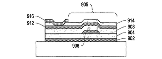
図9Aは、反転、スタガ、エッチング停止または3層TFT(inverted,staggered,etch−stopper or trilayer TFT)901を示す。図9Bは、アモルファスシリコンとは対照的に、多結晶シリコンとともに一般に使用される、トップゲートTFT903を示す。図9Cは、薄膜ダイオード905としばしば呼ばれる、金属−絶縁体−金属(MIM)構造を示す。構造901、903、および905のそれぞれは、トランジスタ518(図6)に見出されるものと比較して、類似した機能、および類似した蒸着/パターニングプロセスを有する、特定の層を含む。これらは、アパーチャ層902と、第1の誘電体層904と、第1の導体層906と、第2の誘電体層908と、第2の導体層912と、第3の誘電体層914と、第3の導体層916とを含む。   FIG. 9A shows an inversion, staggered, etch stop, or three-layer TFT (inverted, staggered, etch-stopper or trilayer TFT) 901. FIG. 9B shows a top gate TFT 903 that is commonly used with polycrystalline silicon as opposed to amorphous silicon. FIG. 9C shows a metal-insulator-metal (MIM) structure, often referred to as a thin film diode 905. Each of the structures 901, 903, and 905 includes specific layers that have similar functions and similar deposition / patterning processes as compared to those found in transistor 518 (FIG. 6). These include an aperture layer 902, a first dielectric layer 904, a first conductor layer 906, a second dielectric layer 908, a second conductor layer 912, and a third dielectric layer 914. And a third conductor layer 916.

トランジスタ518およびプロセスフロー700と比較して、エッチング停止TFT(etch−stopper TFT)901のためのプロセスは、2つの追加の層と、1つの追加のフォトマスクとを追加する。エッチング停止TFT(etch stopper TFT)は、真性アモルファスシリコン層918、およびドープアモルファスシリコン層920という、(1つではなく)2つの別個に蒸着された半導体層を含む。エッチング停止TFT(etch stopper TFT)901は、さらに、真性アモルファスシリコン層918の直後に蒸着される、追加のエッチング停止誘電体層(etch−stopper dielectric layer)922を追加する。エッチング停止TFT(etch stopper TFT)のためのプロセスを継続すると、エッチング停止誘電体層(etch−stopper dielectric layer)922は、通常、TFTの上で、アイランドにパターニングされる。次に、ドープアモルファスシリコン層920が蒸着され、半導体層918および920の両方が、次に、シリコンアイランドにパターニングされる。次に、第2の導体層912が蒸着される。第2の導体層912をソースおよびドレイン領域にパターニング/エッチングするプロセスは、下にあるドープアモルファスシリコン層920のエッチングプロセスを含む。このエッチングプロセスは、エッチング剤がエッチング停止誘電体層(etch stopper dielectric layer)922に到達すると自然に停止し、それにより、手順700のステップ730のソース/ドレインパターニングに比較して、かなり多くの変形形態のための自由度が、(トランジスタの重大な劣化なしに)このプロセスに提供される。ただし、第1および第2の導体層906および912のために使用される材料は、トランジスタ901とトランジスタ518との間で同様であり、さらに、トランジスタのスイッチング特性も同様である。以下の図10で説明するビア構造も、トランジスタ518またはトランジスタ901のいずれかの構造の使用によって、実質的に影響を受けない。   Compared to transistor 518 and process flow 700, the process for etch-stopper TFT 901 adds two additional layers and one additional photomask. The etch stop TFT includes two separately deposited semiconductor layers (instead of one), an intrinsic amorphous silicon layer 918 and a doped amorphous silicon layer 920. The etch stop TFT 901 further adds an additional etch-stopper dielectric layer 922 that is deposited immediately after the intrinsic amorphous silicon layer 918. Continuing the process for the etch stop TFT, the etch-stopper dielectric layer 922 is typically patterned into an island over the TFT. Next, a doped amorphous silicon layer 920 is deposited and both semiconductor layers 918 and 920 are then patterned into silicon islands. Next, a second conductor layer 912 is deposited. The process of patterning / etching the second conductor layer 912 into the source and drain regions includes an etching process of the underlying doped amorphous silicon layer 920. This etch process stops spontaneously when the etchant reaches the etch stop dielectric layer 922, thereby significantly more variations than the source / drain patterning of step 730 of procedure 700. Freedom for form is provided in this process (without significant transistor degradation). However, the materials used for the first and second conductor layers 906 and 912 are the same between the transistor 901 and the transistor 518, and the switching characteristics of the transistor are also the same. The via structure described in FIG. 10 below is also substantially unaffected by the use of either transistor 518 or transistor 901 structure.

図9Bは、共通トップゲート低温多結晶薄膜トランジスタ(common top−gate low−temperature polycrystalline thin film transistor)(LTPS−TFT)903の構造を示す。トランジスタ518(図6)および手順700と比較して、LTPS−TFTでは、半導体層と第1の導体層の順序およびシーケンスが変更される。図9Bは、第1の誘電体層904の直後に蒸着される、多結晶シリコン層924を含む。シリコン層924は、通常、アモルファスシリコン層として蒸着され、次に、エキシマレーザアニーリングによって多結晶シリコンに変換されてから、シリコンアイランドにパターニングされる。多結晶シリコン層のパターニングに続いて、次に、ゲート絶縁層926という追加の層が、一面に覆うやり方で蒸着される。次に、第1の導体層906が蒸着され、ゲート金属を形成するようにパターニングされる。次に、シリコンアイランドのソースおよびドレイン領域が、ホウ素またはリンのいずれかを使用して、イオン打ち込み、プラズマ浸積、またはイオンシャワードーピング技術のいずれかによってドープされる。(ゲート金属の遮蔽によって、ソースおよびドレインの自己整合ドーピングが可能にされる。)次に、第2の誘電体層908が蒸着され、図10に関して以下で説明するM1−M2ビア531に類似した、ビア開口部の組にパターニングされる。次に、第2の導体層912が蒸着され、ソースおよびドレインへの接続を形成するようにパターニングされる。プロセスは、手順700で説明したシーケンスに類似したシーケンスにより、層914および916で完了する。   FIG. 9B shows a structure of a common top-gate low-temperature polycrystal thin film transistor (LTPS-TFT) 903. Compared to transistor 518 (FIG. 6) and procedure 700, the LTPS-TFT changes the order and sequence of the semiconductor layer and the first conductor layer. FIG. 9B includes a polycrystalline silicon layer 924 deposited immediately after the first dielectric layer 904. The silicon layer 924 is typically deposited as an amorphous silicon layer and then converted to polycrystalline silicon by excimer laser annealing and then patterned into silicon islands. Following patterning of the polycrystalline silicon layer, an additional layer, gate insulating layer 926, is then deposited in a manner that covers the entire surface. Next, a first conductor layer 906 is deposited and patterned to form a gate metal. Next, the source and drain regions of the silicon island are doped by either ion implantation, plasma immersion, or ion shower doping techniques using either boron or phosphorus. (Gate metal shielding allows self-aligned doping of the source and drain.) Next, a second dielectric layer 908 is deposited, similar to the M1-M2 via 531 described below with respect to FIG. , Patterned into a set of via openings. Next, a second conductor layer 912 is deposited and patterned to form connections to the source and drain. The process is completed at layers 914 and 916 with a sequence similar to that described in procedure 700.

層924内の多結晶シリコン材料は、トランジスタ518などのアモルファスシリコントランジスタのために利用可能なものよりも、大幅に高いキャリア移動度を有する。結果として、アモルファスシリコントランジスタのために必要とされる面積よりも大幅に少ない面積を使用しながら、類似した電流と、類似したスイッチング速度とを、LTPSトランジスタを使用して駆動することが可能である。高移動度、小面積LTPSトランジスタの使用により、したがって、より小さなピクセルと、より密なピッチと、したがってより高い解像度のフォーマットとを、固定されたサイズの基板内で有する、MEMSベースのシャッタディスプレイを構築することが可能になる。   The polycrystalline silicon material in layer 924 has a significantly higher carrier mobility than is available for amorphous silicon transistors such as transistor 518. As a result, similar currents and similar switching speeds can be driven using LTPS transistors while using significantly less area than is required for amorphous silicon transistors. . The use of a high mobility, small area LTPS transistor thus provides a MEMS-based shutter display with smaller pixels, denser pitch, and therefore higher resolution format within a fixed size substrate. It becomes possible to build.

トランジスタ903などの、LTPSトランジスタを、MEMSベースのシャッタディスプレイに適合させる場合、その他の有用な修正が、フォトパターンおよびプロセスフローに対して行われてもよい。例えば、トランジスタ903のようなLTPSトランジスタとともに使用するための、図10A〜図10Fに示すようなAp−M1ビア533を形成するためには、ビア533の領域内で、多結晶シリコン層924を除去することが適切である。さらに、ビア533の形成においては、第1の誘電体層604を貫通してビアを通常開くのと同じフォトパターンおよびエッチング(ステップ710、図10Bに示す)は、ゲート誘電体層926の蒸着の後まで遅らされてもよい。   When LTPS transistors, such as transistor 903, are adapted to a MEMS-based shutter display, other useful modifications may be made to the photo pattern and process flow. For example, to form an Ap-M1 via 533 as shown in FIGS. 10A-10F for use with an LTPS transistor such as transistor 903, the polysilicon layer 924 is removed within the region of the via 533. It is appropriate to do. Further, in forming the via 533, the same photo pattern and etch (shown in step 710, FIG. 10B) that normally opens the via through the first dielectric layer 604 is the same as the deposition of the gate dielectric layer 926. It may be delayed until later.

当業界で周知であるが、図9には示されていない、薄膜トランジスタの別の一般的な変形形態は、スタガトップゲートアモルファスシリコントランジスタ(staggered top−gate amorphous silicon transistor)である。反転スタガトランジスタ(inverted staggered transistor)518(図6)の、このさらなる変形形態では、2つの導体層の役割が逆にされる。第1の導体層606は、そのすぐ上に蒸着される半導体層610へのソースおよびドレイン接点を形成するために使用される。第2の導体層612は、ゲート構造を形成するために使用される。MEMSベースのシャッタディスプレイをアモルファストップゲートトランジスタ(amorphous top−gate transistor)に適合させるために、走査ライン相互接続506は、好ましくは、第1の導体層606内ではなく、第2の導体層612内にパターニングされてもよい。逆に、データ開相互接続508aまたは事前充電相互接続510などの、その他の相互接続ラインは、好ましくは、第1の導体層606内にパターニングされてもよい。アモルファストップゲートトランジスタ(amorphous top−gate transistor)の使用によって、特定のトランジスタのドレインを駆動アンカー535に接続するための、M1−M2ビア531などの、いくつかのビアの必要がなくなることにより、ピクセル内のいくらかの空間が節約されてもよい。   Another common variant of a thin film transistor that is well known in the art but not shown in FIG. 9 is a staggered top-gate amorphous silicon transistor. In this further variation of the inverted staggered transistor 518 (FIG. 6), the roles of the two conductor layers are reversed. The first conductor layer 606 is used to form source and drain contacts to the semiconductor layer 610 deposited immediately above it. The second conductor layer 612 is used to form a gate structure. In order to adapt the MEMS-based shutter display to an amorphous top-gate transistor, the scan line interconnect 506 is preferably in the second conductor layer 612 rather than in the first conductor layer 606. May be patterned. Conversely, other interconnect lines, such as data open interconnect 508a or precharge interconnect 510, may preferably be patterned in first conductor layer 606. The use of an amorphous top-gate transistor eliminates the need for several vias, such as the M1-M2 via 531, to connect the drain of a particular transistor to the drive anchor 535, thereby enabling the pixel. Some space inside may be saved.

図9Cは、MIM薄膜ダイオード905の構造を示す。トランジスタ518(図6)と比較して、ダイオード905は、半導体層を含まない。代わりに、第2の誘電体材料908のために、材料の特定の選択が使用される。第2の誘電体材料908のために選択される材料としては、漏れやすい誘電体、または電荷を捕獲する機能を有する誘電体のいずれかとしての性能で知られている材料である、Si、Ta、またはダイヤモンド状炭素が挙げられる。これらの材料の蒸着のために使用される技術としては、プラズマアシスト化学気相蒸着法(plasma−assisted chemical vapor deposition)(PECVD)、ホットワイヤ蒸着、または、スパッタリングとそれに続く電気化学的陽極酸化が挙げられる。 FIG. 9C shows the structure of the MIM thin film diode 905. Compared to the transistor 518 (FIG. 6), the diode 905 does not include a semiconductor layer. Instead, a specific selection of materials is used for the second dielectric material 908. The material selected for the second dielectric material 908 is Si 3 N, a material known for its performance as either a leaky dielectric or a dielectric with the function of trapping charge. 4 , Ta 2 O 5 , or diamond-like carbon. Techniques used for the deposition of these materials include plasma-assisted chemical vapor deposition (PECVD), hot wire deposition, or sputtering followed by electrochemical anodization. Can be mentioned.

動作時、MIMダイオード905は、大規模なピクセルアレイ内で達成可能な、選択性、アドレス指定、および/またはコントラストを、パッシブマトリクスの使用に比較して向上するのを補助することが可能な、バリスタとして動作する。ビア構造(以下の図10を参照)を形成するために使用されるプロセスは、ほとんど変更なしに、MIMダイオード905に使用するために適合されてもよい。MIMダイオード905をスイッチ構造として使用して制御マトリクスを生成するのは、より安価な場合があり、その理由は、これらのスイッチは、アモルファスシリコントランジスタ518に比較した場合、1つ少ない蒸着ステップと、1つ少ないフォトマスクとを使用して生成でき、さらに、より容易に達成できるパターニング寸法を有するからである。   In operation, the MIM diode 905 can help improve the selectivity, addressing, and / or contrast achievable within a large pixel array compared to the use of a passive matrix. Acts as a varistor. The process used to form the via structure (see FIG. 10 below) may be adapted for use with the MIM diode 905 with little modification. Using the MIM diode 905 as a switch structure to generate a control matrix may be cheaper because these switches have one less deposition step when compared to the amorphous silicon transistor 518, and This is because it has a patterning dimension that can be generated using one photomask and more easily achieved.

薄膜スイッチ901、903、および905は、薄膜スイッチの構造についての、多くの可能な変形形態のうちの3つの例にすぎない。その他の変形形態が可能であることが、上に記載した例から、および当業者によって、理解されるであろう。上に示した、または手順700内で記載した層よりも多い、または少ない数の層を含む、あるいは、手順700内で説明したステップの順序の変形を含む、類似した構造が構築されてもよい。   Thin film switches 901, 903, and 905 are just three examples of many possible variations on the structure of a thin film switch. It will be appreciated from the examples described above and by those skilled in the art that other variations are possible. Similar structures may be constructed that include more or fewer layers than those shown above or described in procedure 700, or that include variations in the order of steps described in procedure 700. .

図10Aは、特に、トランジスタ間の、またはトランジスタとシャッタ組立体のアンカーとの間の相互接続を補助するために、制御マトリクス500の要素として使用されてもよい、ビア構造のうちのいくつかの断面図を示す。図10Aは、4つの別個のタイプのビア構造を含む。図10Aは、第1の導体層606を第2の導体層612に接続するためのビアである、M1−M2ビア531を含む。図10Aは、アパーチャ層602を第1の導体層606に接続するビアである、Ap−M1ビア533を含む。図10Aは、さらに、シャッタ545と制御マトリクス500との間の、機械的および電気的な、支持または接続を提供する、シャッタアンカー539を示す。図10A内の構造は、あたかもそれらが基板1001上で相互に隣接しているかのように示されているが、これは、共通の高さの基準が提供されてもよいように、例示する目的のためのみである。E−E’またはF−F’などの断面マーカは、図10A〜図10F内のマーカを、図5B/5C内の同じマーカと比較することによって、ピクセル内のこれらの構造の位置的関係を、読者が識別できるようにするために提供されている。   FIG. 10A illustrates some of the via structures that may be used as elements of the control matrix 500, particularly to assist interconnection between transistors or between transistors and anchors of a shutter assembly. A cross-sectional view is shown. FIG. 10A includes four distinct types of via structures. FIG. 10A includes an M1-M2 via 531 that is a via for connecting the first conductor layer 606 to the second conductor layer 612. FIG. 10A includes an Ap-M1 via 533, which is a via that connects the aperture layer 602 to the first conductor layer 606. FIG. FIG. 10A further shows a shutter anchor 539 that provides mechanical and electrical support or connection between the shutter 545 and the control matrix 500. The structures in FIG. 10A are shown as if they are adjacent to each other on the substrate 1001, but this is for illustrative purposes so that a common height reference may be provided. Only for. Cross-sectional markers such as EE ′ or FF ′ can be used to compare the positional relationship of these structures within the pixel by comparing the markers in FIGS. 10A-10F to the same markers in FIGS. 5B / 5C. Provided to help readers identify.

図10Aは、さらに、ボンドパッド1003の断面図を示す。ボンドパッド1003は、第1の導体層606と、ディスプレイの周辺部のあたりに搭載されてもよいドライバチップまたは電圧源との間の電気的接続を容易にする。ボンドパッドは、図5B/5Cには示されていない。   FIG. 10A further shows a cross-sectional view of bond pad 1003. The bond pad 1003 facilitates electrical connection between the first conductor layer 606 and a driver chip or voltage source that may be mounted around the periphery of the display. The bond pads are not shown in FIGS. 5B / 5C.

図10Aに示すビア構造のそれぞれは、いくつかの金属および誘電体層を共通に含む。これらのビア構造のそれぞれは、アパーチャ層602と、第1の誘電体層604と、第1の導体層606と、第2の誘電体層608と、第2の導体層612と、第3の誘電体層614と、第3の導体層616と、シャッタ層807とを含む。   Each of the via structures shown in FIG. 10A includes several metal and dielectric layers in common. Each of these via structures includes an aperture layer 602, a first dielectric layer 604, a first conductor layer 606, a second dielectric layer 608, a second conductor layer 612, and a third A dielectric layer 614, a third conductor layer 616, and a shutter layer 807 are included.

図7で説明した手順700は、図10A内で説明するビア構造のそれぞれを構築するために使用されてもよい。製造プロセスの段階を追った説明が、図10B〜図10F内のビア構造に関して示される。図10B〜図10Fは、さらに、手順のさまざまなステップにおいて適用されるフォトマスクに採用される、一般的な設計ガイドラインも示す。   The procedure 700 described in FIG. 7 may be used to build each of the via structures described in FIG. 10A. A step-by-step description of the manufacturing process is shown with respect to the via structure in FIGS. 10B-10F. 10B-10F also show general design guidelines that are employed in photomasks applied at various steps in the procedure.

図10Bは、手順700のステップ705および710の適用後の、M1−M2ビア531、Ap−M1ビア533、シャッタアンカー539、およびボンドパッド1003の構造を示す。図10A内のビア構造は、アパーチャ層602の一面に覆う蒸着と、それに続く、第1の誘電体層604の一面に覆う蒸着とを受け入れる。図10A内のビア構造は、アパーチャ層602に対する、ステップ705におけるパターニングは、何も必要としない。ビア構造のうちの1つ、すなわち、Ap−M1ビア533のみが、第1の誘電体ステップ(ステップ710)において、いくらかのパターニングを必要とする。Ap−M1533の場合、第1の誘電体層604を貫通してビア開口部がエッチングされ、それにより、Ap−M1ビアを通したアパーチャ層602への、後続の電気的接続が行われることが可能になる。ビアホールの幅は、通常、2〜30ミクロンである。ビアホールは、通常、正方形であるが、長方形のビアも可能である。第1の誘電体層の厚さは、通常、0.1〜2.0ミクロンの範囲内である。   FIG. 10B shows the structure of the M1-M2 via 531, Ap-M1 via 533, shutter anchor 539, and bond pad 1003 after application of steps 700 and 710 of the procedure 700. The via structure in FIG. 10A accepts deposition over one surface of the aperture layer 602 followed by deposition over one surface of the first dielectric layer 604. The via structure in FIG. 10A does not require any patterning in step 705 for the aperture layer 602. Only one of the via structures, Ap-M1 via 533, requires some patterning in the first dielectric step (step 710). In the case of Ap-M1533, the via opening is etched through the first dielectric layer 604, thereby making a subsequent electrical connection to the aperture layer 602 through the Ap-M1 via. It becomes possible. The width of the via hole is usually 2 to 30 microns. Via holes are usually square, but rectangular vias are possible. The thickness of the first dielectric layer is usually in the range of 0.1 to 2.0 microns.

図10Cは、手順700のステップ715の適用後の、M1−M2ビア531、Ap−M1ビア533、シャッタアンカー539、およびボンドパッド1003の構造を示す。図10Cは、既存の層602、604を含む。蒸着された場合、第1の導体層606は、Ap−M1ビア533の第1の誘電体層内に開けられたビアを完全に充填する。好ましい設計ガイドラインは、パターニングされた金属蒸着は、以前のステップで提供されたビアホールを、少なくとも2ミクロンだけ過剰充填しなければならないということを指示する。図10Cは、さらに、シャッタアンカー539においては、第1の導体層606は、蒸着後にエッチングにより完全に除去され、第1の誘電体層604が露出することを示している。第1の導体層606の、すべてのパターニングされた端は、傾斜を付けられている。第1の導体層606内の金属のために利用可能なほとんどの化学エッチング(etch chemistries)は、下にある第1の誘電体層604に対する良好な選択性を有し、そのため、金属エッチングが、下にある誘電体層を、認め得るほどに侵すことはない。好ましい設計指針では、1つの金属層のエッチングが、下にある金属層で停止することを要求される状況を回避する。   FIG. 10C shows the structure of the M1-M2 via 531, Ap-M1 via 533, shutter anchor 539, and bond pad 1003 after application of step 715 of the procedure 700. FIG. 10C includes existing layers 602, 604. When deposited, the first conductor layer 606 completely fills the via opened in the first dielectric layer of the Ap-M1 via 533. Preferred design guidelines indicate that patterned metal deposition must overfill via holes provided in previous steps by at least 2 microns. FIG. 10C further shows that in shutter anchor 539, first conductor layer 606 is completely removed by etching after deposition, exposing first dielectric layer 604. FIG. All patterned edges of the first conductor layer 606 are beveled. Most chemical etches available for the metal in the first conductor layer 606 have good selectivity for the underlying first dielectric layer 604, so that the metal etch is It does not appreciably damage the underlying dielectric layer. Preferred design guidelines avoid situations where etching of one metal layer is required to stop at the underlying metal layer.

図10Dは、手順700のステップ720、725、および730の適用後の、M1−M2ビア531、Ap−M1ビア533、シャッタアンカー539、およびボンドパッド1003の構造を示す。図10Dは、既存の層602、604、および606を含む。ステップ720は、第2の誘電体層608の蒸着と、M1−M2構造531内にビアを開けるためのパターニングとを行うために使用される。一面に覆う(すなわち、パターニングされない)誘電体が、その他のビア構造のすべての上に残ることを許可される。半導体層610は、図10A内のビア構造のいずれにも含まれない。ステップ725において、第1の半導体610は、図10D内の構造のそれぞれから、エッチングにより除去される。ステップ730において、第2の導体層が、第2の誘電体材料608を貫通してエッチングすることによって提供されたM1−M2ビア531を、完全に充填することが許可される。第2の導体層612は、その他のビアの表面から完全に除去され、金属エッチングは、すべての下にある誘電体層上で停止する。   FIG. 10D shows the structure of the M1-M2 via 531, Ap-M1 via 533, shutter anchor 539, and bond pad 1003 after application of steps 720, 725, and 730 of the procedure 700. FIG. 10D includes existing layers 602, 604, and 606. Step 720 is used to perform deposition of the second dielectric layer 608 and patterning to open vias in the M1-M2 structure 531. A dielectric overlying (ie, unpatterned) is allowed to remain on all other via structures. The semiconductor layer 610 is not included in any of the via structures in FIG. 10A. In step 725, the first semiconductor 610 is etched away from each of the structures in FIG. 10D. In step 730, the second conductor layer is allowed to completely fill the M1-M2 via 531 provided by etching through the second dielectric material 608. The second conductor layer 612 is completely removed from the surface of the other vias and the metal etch stops on all underlying dielectric layers.

図10Eは、手順700のステップ735および740の適用後の、M1−M2ビア531、Ap−M1ビア533、シャッタアンカー539、およびボンドパッド1003の構造を示す。図10Eは、既存の層602、604、606、608、および612を含む。ステップ735の目的は、M1−M2ビア531およびAp−M1ビア533において示すように、第3の誘電体層614を使用して、すべてのトランジスタおよび相互接続材料の表面を保護し、保護することである。プロセスのステップ740において、第3の導体層616は、M1−M2ビア531およびAp−M1ビア533に含まれず、したがって、M1−M2ビア531およびAp−M1ビア533から完全に除去される。第3の誘電体層614および第3の導体層616の両方は、シャッタアンカー539の領域内で除去される。   FIG. 10E shows the structure of the M1-M2 via 531, Ap-M1 via 533, shutter anchor 539, and bond pad 1003 after application of steps 700 and 740 of the procedure 700. FIG. 10E includes existing layers 602, 604, 606, 608, and 612. The purpose of step 735 is to protect and protect the surface of all transistors and interconnect materials using a third dielectric layer 614, as shown in M1-M2 via 531 and Ap-M1 via 533. It is. In process step 740, the third conductor layer 616 is not included in the M1-M2 via 531 and Ap-M1 via 533 and is therefore completely removed from the M1-M2 via 531 and Ap-M1 via 533. Both the third dielectric layer 614 and the third conductor layer 616 are removed in the region of the shutter anchor 539.

図10Eは、ボンドパッド1003の完成を示す。ボンドパッド1003の目的は、ディスプレイの周辺部において、下にある導体層への電気的接続を作る目的で、第3の誘電体層614を貫通するビアを提供することである。ボンドパッド1003は、第3の導体層616と第1の導体層606との間の、電気的ビアまたは接点を示す。ステップ735内で行われるビアエッチングステップは、第3の誘電体層614と第2の誘電体層608との両方を貫通してエッチングし、任意の下にある金属上で終了するように設計されるという点で、独特である。シャッタアンカー539の領域内では、誘電体層614および608のために使用されるエッチングは、第1の誘電体層604のすべてではなく、途中までをエッチングする。ステップ740は、第3の導体層616を使用した、ボンドパッド1003の充填を提供する。第3の導体層616は、ディスプレイの周辺部でボンドパッドを覆って保護するようにパターニングされる。   FIG. 10E shows the completion of the bond pad 1003. The purpose of the bond pad 1003 is to provide a via through the third dielectric layer 614 in order to make an electrical connection to the underlying conductor layer at the periphery of the display. Bond pad 1003 represents an electrical via or contact between third conductor layer 616 and first conductor layer 606. The via etch step performed within step 735 is designed to etch through both the third dielectric layer 614 and the second dielectric layer 608 and finish on any underlying metal. In that it is unique. Within the region of the shutter anchor 539, the etch used for the dielectric layers 614 and 608 etches halfway but not all of the first dielectric layer 604. Step 740 provides filling of the bond pad 1003 using the third conductor layer 616. The third conductor layer 616 is patterned to cover and protect the bond pads at the periphery of the display.

図10Fは、手順700のステップ745および750の適用後の、M1−M2ビア531、Ap−M1ビア533、シャッタアンカー539、およびボンドパッド1003の構造を示す。図10Eは、既存の層602、604、606、608、612、614、および616を含む。ステップ745の犠牲層805は、シャッタおよびロードビームの機械的連結を形成するシャッタアンカー539以外における、すべての構造を、覆うこと、または保護することが許可される。この犠牲層の詳細は、図12に関して後で示す。ステップ750は、図12に関して詳述する、シャッタ材料の蒸着およびパターニングを含む。   FIG. 10F shows the structure of the M1-M2 via 531, Ap-M1 via 533, shutter anchor 539, and bond pad 1003 after application of steps 700 and 750 of the procedure 700. FIG. 10E includes existing layers 602, 604, 606, 608, 612, 614, and 616. The sacrificial layer 805 in step 745 is allowed to cover or protect all structures except the shutter anchor 539 that forms the mechanical connection of the shutter and load beam. Details of this sacrificial layer are given later with respect to FIG. Step 750 includes the deposition and patterning of the shutter material, as described in detail with respect to FIG.

これらのビア構造の形成における最終ステップは、手順700のステップ755(犠牲層の除去)として説明される。ステップ755の完了後は、すべてのビアの最終構造が、図10Aに示すように完成する。   The final step in the formation of these via structures is described as step 755 (sacrificial layer removal) of procedure 700. After completion of step 755, the final structure of all vias is complete as shown in FIG. 10A.

その他の変形形態が可能であることが理解されるべきである。図10Aを図8Hと比較すると、シャッタアンカーと駆動アンカーとは異なる金属層において構築されているということがわかる。駆動アンカー535は、第1の導体層606に直接接続されるのに対して、シャッタアンカー535は、アパーチャ層に直接接続される。シャッタアンカーと駆動アンカーとが、第1の導体層606などの、同じ金属層に取り付けられる実施形態も可能であり、それにより、シャッタ組立体504内での任意の機械的高さの差が減らされてもよい。   It should be understood that other variations are possible. Comparing FIG. 10A to FIG. 8H, it can be seen that the shutter anchor and the drive anchor are constructed in different metal layers. The drive anchor 535 is directly connected to the first conductor layer 606, while the shutter anchor 535 is directly connected to the aperture layer. Embodiments in which the shutter anchor and drive anchor are attached to the same metal layer, such as the first conductor layer 606, are possible, thereby reducing any mechanical height difference within the shutter assembly 504. May be.

図8A〜図8H内にも、図10A〜図10E内にも示されていないのは、走査ライン相互接続506、データライン相互接続508a、または事前充電相互接続510などの、相互接続ラインの形成である。これらの相互接続は、アパーチャ層602、第1の導体層606、第2の導体層608、第3の導体層616、またはシャッタ層807内などの、制御マトリクス500の任意の導体層内で、適切なフォトパターンを作成することによって、手順700内で、実現可能に作成されてもよいということが理解されるべきである。   Not shown in FIGS. 8A-8H or FIGS. 10A-10E is the formation of interconnect lines, such as scan line interconnect 506, data line interconnect 508a, or precharge interconnect 510. It is. These interconnects are in any conductor layer of the control matrix 500, such as in the aperture layer 602, the first conductor layer 606, the second conductor layer 608, the third conductor layer 616, or the shutter layer 807, It should be understood that it may be made feasible within procedure 700 by creating an appropriate photo pattern.

図11は、MEMSベースのシャッタディスプレイの一実装による、基板1103およびアパーチャ層1106上に構築される、シャッタ1101と、コンプライアントビーム1102と、アンカー構造1104とを含む、複合シャッタ組立体1100の詳細断面を示す。複合シャッタ組立体の要素は、第1のメカニカル層1105と、導体層1107と、第2のメカニカル層1109と、封入誘電体(encapsulating dielectric)1111とを含む。メカニカル層のうちの一方または両方は、シャッタ組立体のための主要耐荷重および機械的作動部材を構成するため、メカニカル層1105または1109のうちの少なくとも一方は、0.15ミクロンを超える厚さに蒸着される。メカニカル層1105および1109のための候補となる材料としては、以下に限定されるものではないが、Al、Cu、Ni、Cr、Mo、Ti、Ta、Nb、Ndなどの金属またはその合金、Al、SiO、Ta、またはSiなどの誘電体材料、あるいは、ダイヤモンド状炭素、Si、Ge、GaAs、CdTeなどの半導体材料またはその合金が挙げられる。作動要素上に、および作動要素から、電荷を運ぶために、導体層1107などの、少なくとも1つの層は、導電性でなければならない。候補となる材料としては、以下に限定されるものではないが、Al、Cu、Ni、Cr、Mo、Ti、Ta、Nb、Nd、またはその合金、あるいは、ダイヤモンド状炭素、Si、Ge、GaAs、CdTeなどの半導体材料またはその合金(特に、リン、ヒ素、ホウ素、またはアルミニウムなどの不純物を使用して半導体がドープされている場合)が挙げられる。図11は、同様の厚さと機械的特性とを有するメカニカル層1105および1109が、導体層1107の両側上に蒸着された、複合物のためのサンドイッチ構成を示す。そのようなサンドイッチ構造は、蒸着の後に残る応力、および/または、温度変化によって加えられる応力が、シャッタ組立体1100の曲げまたは反りを発生させるように働かないことを確実にするために役立つ。 FIG. 11 shows details of a composite shutter assembly 1100 that includes a shutter 1101, a compliant beam 1102, and an anchor structure 1104 built on a substrate 1103 and an aperture layer 1106, according to one implementation of a MEMS-based shutter display. A cross section is shown. The elements of the composite shutter assembly include a first mechanical layer 1105, a conductor layer 1107, a second mechanical layer 1109, and an encapsulating dielectric 1111. Since one or both of the mechanical layers constitutes the primary load bearing and mechanical actuating member for the shutter assembly, at least one of the mechanical layers 1105 or 1109 has a thickness greater than 0.15 microns. Vapor deposited. Candidate materials for mechanical layers 1105 and 1109 include, but are not limited to, metals such as Al, Cu, Ni, Cr, Mo, Ti, Ta, Nb, Nd or alloys thereof, Al A dielectric material such as 2 O 3 , SiO 2 , Ta 2 O 5 , or Si 3 N 4 , a semiconductor material such as diamond-like carbon, Si, Ge, GaAs, or CdTe or an alloy thereof can be given. In order to carry charge on and from the actuation element, at least one layer, such as the conductor layer 1107, must be conductive. Candidate materials include, but are not limited to, Al, Cu, Ni, Cr, Mo, Ti, Ta, Nb, Nd, or alloys thereof, or diamond-like carbon, Si, Ge, GaAs , Semiconductor materials such as CdTe or alloys thereof (especially when the semiconductor is doped using impurities such as phosphorus, arsenic, boron, or aluminum). FIG. 11 shows a sandwich configuration for a composite in which mechanical layers 1105 and 1109 having similar thickness and mechanical properties are deposited on both sides of the conductor layer 1107. Such a sandwich structure helps to ensure that stresses remaining after deposition and / or stresses applied due to temperature changes do not act to cause the shutter assembly 1100 to bend or warp.

シャッタ1101の薄膜スタック内の材料のうちの少なくとも1つは、光をブロックするもの、すなわち、可視スペクトル内で不透明なものでなければならない。シャッタ内の、メカニカル層1105内で、または導体層1107のために、金属が使用される場合、それらは、入射光の95%よりも多くをブロックするのに効果的である。半導体材料も、特に、それらが0.5ミクロンを超える厚さで提供される場合、可視光に対して不透明であってもよい。   At least one of the materials in the thin film stack of shutter 1101 must block light, i.e., be opaque in the visible spectrum. If metals are used in the shutter, in the mechanical layer 1105, or for the conductor layer 1107, they are effective to block more than 95% of the incident light. Semiconductor materials may also be opaque to visible light, especially if they are provided with a thickness greater than 0.5 microns.

好ましくは、シャッタ1101内の材料のうちの少なくとも1つは、さらに、光を吸収するものであり、それにより入射光は、単に反射される代わりに、実質的に吸収される(多くの金属は、吸収ではなく、主に反射によって、光をブロックする)。層1105、1107、または1109のために有用な、いくつかの金属合金は、光を吸収するのに特に効果的である。そのような金属合金としては、以下に限定されるものではないが、MoCr、MoW、MoTi、MoTa、TiW、およびTiCr合金が挙げられ、これらは、場合によっては、入射光の30%よりも多くを吸収する。アモルファスまたは多結晶のSi、Ge、CdTe、InGaAs、コロイド黒鉛(炭素)などの半導体材料、およびSiGeなどの合金も、光を吸収するのに効果的である。   Preferably, at least one of the materials in shutter 1101 is further one that absorbs light so that incident light is substantially absorbed instead of simply reflected (many metals are Block light, mainly by reflection, not absorption). Some metal alloys, useful for layers 1105, 1107, or 1109, are particularly effective at absorbing light. Such metal alloys include, but are not limited to, MoCr, MoW, MoTi, MoTa, TiW, and TiCr alloys, which in some cases may be greater than 30% of incident light. To absorb. Amorphous or polycrystalline Si, Ge, CdTe, InGaAs, semiconductor materials such as colloidal graphite (carbon), and alloys such as SiGe are also effective in absorbing light.

一部の実装では、サンドイッチの外側は導体層からなり、サンドイッチの内側はメカニカル層からなるように、複合シャッタ組立体1100内の層の順序が逆にされてもよい。   In some implementations, the order of the layers in the composite shutter assembly 1100 may be reversed such that the outside of the sandwich consists of a conductor layer and the inside of the sandwich consists of a mechanical layer.

シャッタ1101を通した光の透過量のさらなる減少、および/または、光の吸収量のさらなる増加が望まれる場合、追加の吸収性コーティングが、複合シャッタ1101の上面または底面のいずれか、あるいは両方の面に追加されてもよい(図示せず)。光の吸収に効果的な、いくつかの蒸着される金属コーティングとしては、以下に限定されるものではないが、Ni、Cr、Ti、Zr、ならびに、MoCr、MoW、MoTi、MoTa、TiW、TiCrなどの合金が挙げられる。粗い金属コーティングは、吸収率を向上させる。そのような粗い表面は、高ガス圧(20ミリトール(mtorr)を超えるスパッタリング環境)内でのスパッタ蒸着によって生成されてもよい。   If further reduction in the amount of light transmitted through the shutter 1101 and / or further increase in the amount of light absorption is desired, an additional absorbent coating may be provided on either or both of the top and bottom surfaces of the composite shutter 1101. It may be added to the surface (not shown). Some vapor deposited metal coatings that are effective in absorbing light include, but are not limited to, Ni, Cr, Ti, Zr, and MoCr, MoW, MoTi, MoTa, TiW, TiCr. And alloys thereof. A rough metal coating improves the absorption rate. Such a rough surface may be produced by sputter deposition in a high gas pressure (sputtering environment above 20 mtorr).

アモルファスまたは多結晶のSi、Ge、CdTe、InGaAs、コロイド黒鉛(炭素)などの、シャッタ組立体1100のための半導体コーティング材料、およびSiGeなどの合金も、光を吸収するのに効果的である。以下に限定されるものではないが、CuO、NiO、Cr、AgO、SnO、ZnO、TiO、Ta、MoO、CrN、TiN、またはTaNを含む、金属酸化物または窒化物を材料とするコーティングも、光を吸収するのに効果的である。これらの酸化物または窒化物の吸収は、酸化物が非化学量論的なやり方−しばしば、スパッタリングまたは蒸発(evaporation)による−で調整または蒸着される場合、特に、蒸着プロセスによって格子内の酸素または窒素の不足がもたらされる場合に、向上する。 Semiconductor coating materials for the shutter assembly 1100, such as amorphous or polycrystalline Si, Ge, CdTe, InGaAs, colloidal graphite (carbon), and alloys such as SiGe are also effective in absorbing light. Metal oxides or nitrides including, but not limited to, CuO, NiO, Cr 2 O 3 , AgO, SnO, ZnO, TiO, Ta 2 O 5 , MoO 3 , CrN, TiN, or TaN A coating made of a material is also effective in absorbing light. The absorption of these oxides or nitrides is particularly important when the oxide is tuned or deposited in a non-stoichiometric manner—often by sputtering or evaporation—especially by the deposition process. Improves when nitrogen deficiency results.

サーメット材料のクラスも、シャッタ組立体1100のための吸収性コーティングとして効果的である。サーメットは、通常、酸化物または窒化物の母体内に、小さな金属粒子が浮遊させられた、複合材料である。例としては、Cr母体内のCr粒子、またはSiO母体内のCr粒子が挙げられる。母体内で浮遊させられるその他の金属粒子は、Ni、Ti、Au、Ag、Mo、Nb、および炭素であってもよい。その他の母体材料としては、TiO、Ta、Al、およびSiが挙げられる。 A class of cermet materials is also effective as an absorbent coating for the shutter assembly 1100. Cermet is a composite material, usually with small metal particles suspended in an oxide or nitride matrix. Examples include Cr particles in the Cr 2 O 3 matrix or Cr particles in the SiO 2 matrix. Other metal particles suspended in the mother body may be Ni, Ti, Au, Ag, Mo, Nb, and carbon. Examples of other base materials include TiO 2 , Ta 2 O 5 , Al 2 O 3 , and Si 3 N 4 .

シャッタ組立体1100を光吸収性材料でコーティングする目的のために、光吸収性染料を含む、ポリマーコーティングまたは樹脂も、使用されてもよい。   For the purpose of coating the shutter assembly 1100 with a light absorbing material, a polymer coating or resin comprising a light absorbing dye may also be used.

適切な薄膜材料間での光の相殺的干渉を利用することによる、多層吸収構造から、シャッタコーティングを作成することも可能である。代表的な実装としては、酸化物または窒化物の部分反射層(partially reflecting layer)を、適切な反射率の金属とともに使用することが挙げられる。酸化物は、例えば、CrO、TiO、Al、またはSiOなどの金属酸化物、あるいは、Siのような窒化物であってもよく、金属は、Cr、Mo、Al、Ta、Tiのような適切な金属であってもよい。一実装では、金属層が最初に蒸着され、それに続いて、金属酸化物または窒化物が蒸着される。両方の場合に、2層の吸収率は、酸化物または窒化物層の厚さが、0.55ミクロンの4分の1を酸化物層の屈折率で割った値に実質的に等しいように選択される場合に、最適化されてもよい。 It is also possible to make shutter coatings from multilayer absorption structures by utilizing destructive interference of light between suitable thin film materials. A typical implementation includes the use of an oxide or nitride partially reflecting layer with a metal of appropriate reflectivity. The oxide may be, for example, a metal oxide such as CrO 2 , TiO 2 , Al 2 O 3 , or SiO 2 , or a nitride such as Si 3 N 4 , and the metal may be Cr, Mo, A suitable metal such as Al, Ta, Ti may be used. In one implementation, the metal layer is deposited first, followed by the metal oxide or nitride. In both cases, the absorption rate of the two layers is such that the oxide or nitride layer thickness is substantially equal to a quarter of 0.55 microns divided by the refractive index of the oxide layer. If selected, it may be optimized.

一部の適用例のためには、シャッタ1101の一方の面は吸収性であり、反対側の面は反射器であることが望ましい。図11内のメカニカル層1105または1109のうちのいずれか1つが、滑らかな金属からなる場合、十分な反射能がもたらされる。他の適用例では、シャッタの上部または下部のいずれかに、反射性コーティングを特に追加することが望ましい場合がある。良好な反射性コーティングとしては、Al、Au、Ag、Cr、Ni、またはNbの滑らかな蒸着に、多くの場合、酸化物または誘電体がさらにコーティングされたものが挙げられる。   For some applications, it is desirable that one surface of the shutter 1101 is absorptive and the opposite surface is a reflector. If either one of the mechanical layers 1105 or 1109 in FIG. 11 is made of a smooth metal, sufficient reflectivity is provided. In other applications, it may be desirable to specifically add a reflective coating either on the top or bottom of the shutter. Good reflective coatings include a smooth deposition of Al, Au, Ag, Cr, Ni, or Nb, often further coated with an oxide or dielectric.

シャッタ組立体1100は、封入誘電体層(encapsulating dielectric layer)1111を含む。誘電体コーティングは、シャッタおよびビームの、底面と上面と側面とが、すべて均一にコーティングされるように、コンフォーマルなやり方で適用されてもよい。そのような薄膜は、Al、Cr、TiO、HfO、V、Nb、Ta、SiO、またはSiなどの絶縁体の、熱酸化および/またはコンフォーマル化学気相蒸着法によって、あるいは、同様の材料を、原子層蒸着を使用して蒸着することによって、成長させられてもよい。誘電体コーティング層は、10nm〜1ミクロンの範囲内の厚さで適用されてもよい。場合によっては、側壁上に誘電体コーティングを蒸着するために、スパッタリングおよび蒸発(evaporation)が使用されてもよい。 The shutter assembly 1100 includes an encapsulating dielectric layer 1111. The dielectric coating may be applied in a conformal manner so that the bottom and top and sides of the shutter and beam are all uniformly coated. Such thin films are made of insulators such as Al 2 O 3 , Cr 2 O 3 , TiO 2 , HfO 2 , V 2 O 5 , Nb 2 O 5 , Ta 2 O 5 , SiO 2 , or Si 3 N 4. May be grown by thermal oxidation and / or conformal chemical vapor deposition or by depositing similar materials using atomic layer deposition. The dielectric coating layer may be applied with a thickness in the range of 10 nm to 1 micron. In some cases, sputtering and evaporation may be used to deposit a dielectric coating on the sidewalls.

図12A〜図12Dは、シャッタ1101と、コンプライアントビーム1102と、アンカー構造1104とを含む、シャッタ組立体1100を、基板1103およびアパーチャ層1106の上に構築するためのプロセスを示す。これは、行および列のメタライゼーションと、任意選択でTFTとが、ガラス基板上にすでに製造された時点の後に開始される、例えば、手順700のステップ745から開始される、プロセスである。   12A-12D illustrate a process for constructing a shutter assembly 1100 that includes a shutter 1101, a compliant beam 1102, and an anchor structure 1104 over a substrate 1103 and an aperture layer 1106. This is a process that begins after the point where row and column metallization and, optionally, TFTs are already fabricated on a glass substrate, eg, starting at step 745 of procedure 700.

図12Aは、本発明の例示的実施形態による、シャッタ組立体1100を形成するプロセスの第1ステップの断面図である。図12Aに示すように、犠牲層1113が蒸着され、パターニングされる。ポリイミドが好ましい犠牲材料である。その他の、候補となる犠牲材料としては、ポリアミド、フルオロポリマー、ベンゾシクロブテン、ポリフェニルキノキシレン(polyphenylquinoxylene)、パリレン、ポリノルボルネンなどの、ポリマー材料が挙げられる。これらの材料は、粗い表面を平坦化する機能と、250Cを超える処理温度において機械的完全性を維持する機能と、エッチングの容易さ、および/または、除去中の熱分解の容易さとから選ばれている。代替の犠牲層は、ポリ酢酸ビニル、ポリビニルエチレン(polyvinyl ethylene)、フェノールまたはノボラック樹脂などの、フォトレジストに見出すことができるが、それらの使用は、通常、350C未満の温度に限定される。代替の犠牲層はSiOであり、SiOは、その除去に使用されるフッ化水素酸溶液に対して、他の電子または構造層が耐性を有する限り、優先的に除去されてもよい(Siは、そのような耐性を有する)。別の代替の犠牲層はシリコンであり、シリコンは、その除去に使用されるフッ素プラズマまたはXeFに対して、他の電子および構造層が耐性を有する限り、優先的に除去されてもよい(ほとんどの金属および/またはSiは、そのような耐性を有する)。さらに別の代替の犠牲層はアルミニウムであり、アルミニウムは、強塩基(高濃度NaOH)溶液に対して、他の電子または構造層が耐性を有する限り、優先的に除去されてもよい(Cr、Ni、Mo、Ta、およびSiは、そのような耐性を有する)。さらに別の代替の犠牲層は銅であり、銅は、硝酸または硫酸溶液に対して、他の電子または構造層が耐性を有する限り、優先的に除去されてもよい(Cr、Ni、およびSiは、そのような耐性を有する)。 FIG. 12A is a cross-sectional view of a first step in the process of forming the shutter assembly 1100, according to an illustrative embodiment of the invention. As shown in FIG. 12A, a sacrificial layer 1113 is deposited and patterned. Polyimide is a preferred sacrificial material. Other candidate sacrificial materials include polymeric materials such as polyamides, fluoropolymers, benzocyclobutene, polyphenylquinoxylene, parylene, polynorbornene, and the like. These materials are selected for their ability to planarize rough surfaces, maintain mechanical integrity at processing temperatures in excess of 250C, ease of etching, and / or ease of thermal decomposition during removal. ing. Alternative sacrificial layers can be found in photoresists such as polyvinyl acetate, polyvinyl ethylene, phenol or novolac resins, but their use is usually limited to temperatures below 350C. Sacrificial layer alternative is SiO 2, SiO 2, to the hydrofluoric acid solution used for its removal, other electronic or structural layers as long as they have a resistance, which may be preferentially removed ( Si 3 N 4 has such resistance). Another alternative sacrificial layer is silicon, which may be removed preferentially as long as other electron and structural layers are resistant to the fluorine plasma or XeF 2 used for its removal ( Most metals and / or Si 3 N 4 have such resistance). Yet another alternative sacrificial layer is aluminum, which may be preferentially removed as long as other electronic or structural layers are resistant to strong base (high NaOH) solutions (Cr, Ni, Mo, Ta, and Si have such resistance). Yet another alternative sacrificial layer is copper, which may be preferentially removed as long as other electronic or structural layers are resistant to nitric or sulfuric acid solutions (Cr, Ni, and Si). Have such resistance).

次に、犠牲層1113は、アンカー領域1104において穴またはビアを露出するようにパターニングされる。好ましいポリイミド材料およびその他のポリマー樹脂は、(紫外線フォトマスクを通して露出された領域が、現像剤溶液内で優先的に除去されることを可能にする)光活性物質を含むように配合されていてもよい。その他の犠牲層1113は、追加のフォトレジストの層で犠牲層をコーティングし、フォトレジストをフォトパターニングし、最後に、フォトレジストをエッチングマスクとして使用することによって、パターニングされてもよい。その他の犠牲層は、ハードマスクを使用して犠牲層をコーティングすることによってパターニングされてもよく、ハードマスクは、SiOの、またはクロムなどの金属の、薄層であってもよい。次に、フォトレジストと湿式化学エッチングとを使用して、フォトパターンがハードマスクに転写される。ハードマスク内に作られるパターンは、ドライケミカル、異方性、またはプラズマエッチング(犠牲層内に非常に深く狭いアンカー穴を付与するために使用可能な技術)に対して、非常に耐性があってもよい。 Next, the sacrificial layer 1113 is patterned to expose holes or vias in the anchor region 1104. Preferred polyimide materials and other polymer resins may be formulated to contain a photoactive material (which allows the areas exposed through the UV photomask to be preferentially removed in the developer solution). Good. Other sacrificial layers 1113 may be patterned by coating the sacrificial layer with an additional layer of photoresist, photo-patterning the photoresist, and finally using the photoresist as an etch mask. Other sacrificial layers may be patterned by coating the sacrificial layer using a hard mask, and the hard mask may be a thin layer of SiO 2 or a metal such as chromium. The photo pattern is then transferred to the hard mask using photoresist and wet chemical etching. The pattern created in the hard mask is very resistant to dry chemical, anisotropic, or plasma etching (a technique that can be used to provide very deep and narrow anchor holes in the sacrificial layer). Also good.

アンカー1104またはビア領域が犠牲層内で開けられた後は、露出された、下にある導体表面1114が、表面酸化物層をすべて除去するために、化学的に、または、プラズマのスパッタリング効果によって、エッチングされてもよい。そのような接点エッチングステップは、下にある導体と、シャッタ材料との間の、オーム接触を向上させる。   After the anchor 1104 or via region is opened in the sacrificial layer, the exposed underlying conductor surface 1114 may be removed chemically or by plasma sputtering effects to remove any surface oxide layers. Etching may be performed. Such a contact etch step improves ohmic contact between the underlying conductor and the shutter material.

犠牲層のパターニングの後は、フォトレジスト層またはハードマスクは、溶剤洗浄または酸エッチングのいずれかを使用して、すべて除去されてもよい。   After sacrificial layer patterning, the photoresist layer or hard mask may all be removed using either solvent cleaning or acid etching.

次に、シャッタ組立体1100を構築するためのプロセス内で、図12Bに示すように、シャッタ材料が蒸着される。シャッタ組立体1100は、複数の薄膜1105、1107、および1109から構成される。好ましい実施形態では、第1のメカニカル層1105は、アモルファスシリコン層であって、最初に蒸着され、続いて、アルミニウムからなる導体層1107が蒸着され、続いて、アモルファスシリコンの第2の層1109が蒸着される。シャッタ材料1105、1107、および1109のために使用される蒸着温度は、犠牲層の物理的劣化が発生する温度よりも下である。例えば、ポリイミドは、400Cよりも上の温度で分解することが知られている。シャッタ材料1105、1107、および1109は、400Cよりも下の温度で蒸着されてもよく、したがって、ポリイミドを犠牲材料として使用することが許可される。水素化アモルファスシリコンは、250〜350Cの範囲内の温度で、シランガスからの、プラズマアシスト化学気相蒸着法(plasma−assisted chemical vapor deposition)(PECVD)を使用して、比較的応力のない状態内で、0.15〜3ミクロンの範囲内の厚さに成長させられることが可能なので、層1105および1109のための有用な機械的材料である。ホスフィンガス(PH3)がドーパントとして使用され、それにより、アモルファスシリコンは、1Ω−cm未満の抵抗率を有するように成長させられることが可能となる。代替の実施形態では、同様のPECVD技術が、メカニカル層1105としての、Si、シリコンリッチSi、またはSiO材料の蒸着のために、あるいは、メカニカル層1105のための、ダイヤモンド状炭素、Ge、SiGe、CdTe、またはその他の半導体材料の蒸着のために、使用されてもよい。PECVD蒸着技術の利点は、蒸着がかなりコンフォーマルでありうるということ、すなわち、さまざまな傾斜面や、狭いビアホールの内面をコーティングすることが可能であるということである。犠牲層内に切り込むアンカーまたはビアホールが、垂直側壁の近くに存在する場合でさえ、PECVD技術により、アンカーの下と上の水平面の間で連続的なコーティングを提供することが可能である。 Next, in the process for constructing the shutter assembly 1100, shutter material is deposited as shown in FIG. 12B. The shutter assembly 1100 includes a plurality of thin films 1105, 1107, and 1109. In a preferred embodiment, the first mechanical layer 1105 is an amorphous silicon layer, first deposited, followed by a conductor layer 1107 made of aluminum, followed by a second layer 1109 of amorphous silicon. Vapor deposited. The deposition temperature used for the shutter materials 1105, 1107, and 1109 is below the temperature at which physical degradation of the sacrificial layer occurs. For example, polyimide is known to decompose at temperatures above 400C. Shutter materials 1105, 1107, and 1109 may be deposited at temperatures below 400C, thus permitting the use of polyimide as a sacrificial material. Hydrogenated amorphous silicon is in a relatively stress free state using plasma-assisted chemical vapor deposition (PECVD) from silane gas at temperatures in the range of 250-350C. Is a useful mechanical material for layers 1105 and 1109 because it can be grown to a thickness in the range of 0.15 to 3 microns. Phosphine gas (PH3) is used as a dopant, which allows amorphous silicon to be grown to have a resistivity of less than 1 Ω-cm. In alternative embodiments, similar PECVD techniques may be used for the deposition of Si 3 N 4 , silicon-rich Si 3 N 4 , or SiO 2 material as the mechanical layer 1105, or diamond for the mechanical layer 1105. It may be used for the deposition of gaseous carbon, Ge, SiGe, CdTe, or other semiconductor materials. The advantage of PECVD deposition technology is that the deposition can be fairly conformal, i.e. it is possible to coat various inclined surfaces and the inner surface of narrow via holes. Even if anchors or via holes that cut into the sacrificial layer are present near the vertical sidewalls, PECVD technology can provide a continuous coating between the horizontal plane below and above the anchor.

PECVD技術に加えて、シャッタ層1105または1109の成長のために利用可能な代替の技術としては、RFまたはDCスパッタリング、有機金属化学気相蒸着法、蒸発(evaporation)、電気めっきまたは無電界めっきが挙げられる。   In addition to PECVD techniques, alternative techniques available for the growth of shutter layer 1105 or 1109 include RF or DC sputtering, metal organic chemical vapor deposition, evaporation, electroplating or electroless plating. Can be mentioned.

導体層1107のためには、Alなどの金属薄膜が好ましいが、Cu、Ni、Mo、またはTaなどの代替物が選択されてもよい。そのような導体材料を含めることにより、シャッタ材料の全体的なシート抵抗を減少させるということ、および、シャッタ材料を通した可視光の通過をブロックするのに役立つということの、2つの目的が果たされる。(アモルファスシリコンは、2ミクロン未満の厚さに成長させられた場合、可視光をある程度透過する可能性がある。)導体材料は、スパッタリングにより、あるいは、よりコンフォーマルなやり方では、化学気相蒸着法、電気めっき、または無電界めっきにより蒸着されてもよい。   A metal thin film such as Al is preferred for the conductor layer 1107, but alternatives such as Cu, Ni, Mo, or Ta may be selected. The inclusion of such conductive material serves two purposes: reducing the overall sheet resistance of the shutter material and helping to block the passage of visible light through the shutter material. It is. (Amorphous silicon may transmit some visible light when grown to a thickness of less than 2 microns.) Conductive materials may be chemical vapor deposited by sputtering or in a more conformal manner. It may be deposited by method, electroplating, or electroless plating.

シャッタ組立体1100を構築するためのプロセスは、図12Cに継続される。犠牲層1113がまだウエハ上にある間に、シャッタ層1105、1107、および1109は、フォトマスクされ、エッチングされる。最初に、フォトレジスト材料が塗布され、次に、フォトマスクを通して露光され、次に、現像されて、エッチングマスクが形成される。アモルファスシリコン、窒化シリコン、および酸化シリコンは、次に、フッ素ベースのプラズマ化学の中でエッチングされてもよい。SiOメカニカル層は、HF湿式化学を使用してエッチングされてもよく、導体層内の任意の金属は、湿式化学または塩素ベースのプラズマ化学を使用してエッチングされてもよい。 The process for building the shutter assembly 1100 continues in FIG. 12C. The shutter layers 1105, 1107, and 1109 are photomasked and etched while the sacrificial layer 1113 is still on the wafer. First, a photoresist material is applied, then exposed through a photomask, and then developed to form an etching mask. Amorphous silicon, silicon nitride, and silicon oxide may then be etched in fluorine-based plasma chemistry. The SiO 2 mechanical layer may be etched using HF wet chemistry and any metal in the conductor layer may be etched using wet chemistry or chlorine based plasma chemistry.

図12Cにおいて、フォトマスクを通して適用されるパターン形状は、シャッタ組立体1100のアクチュエータおよびシャッタ内の、剛性、コンプライアンス、および電圧応答などの、機械的特性に影響を及ぼす。シャッタ組立体1100は、断面図に示す、コンプライアントビーム1102を含む。コンプライアントビーム1102は、シャッタ材料の幅が、全高または厚さよりも小さいように形作られる。ビーム寸法比は、少なくとも1.4:1(ビーム1102の幅よりも高さまたは厚さの方が大きい)に維持することが好ましい。   In FIG. 12C, the pattern shape applied through the photomask affects mechanical properties, such as stiffness, compliance, and voltage response, within the actuator and shutter of the shutter assembly 1100. The shutter assembly 1100 includes a compliant beam 1102 shown in a cross-sectional view. The compliant beam 1102 is shaped such that the width of the shutter material is less than the total height or thickness. The beam size ratio is preferably maintained at least 1.4: 1 (height or thickness greater than beam 1102 width).

シャッタ組立体1100を構築するためのプロセスは、図12Dに示すように継続される。犠牲層1113は除去され、それにより、すべての可動部品が、アンカー点以外において、基板1103から解放される。ポリイミド犠牲材料は、好ましくは、酸素プラズマ内で除去される。犠牲層1113のために使用されるその他のポリマー材料も、酸素プラズマ内で除去されてもよく、または場合によっては、熱分解によって除去されてもよい。一部の犠牲層1113(SiOなど)は、湿式化学エッチングによって、または気相エッチングによって除去されてもよい。 The process for building the shutter assembly 1100 continues as shown in FIG. 12D. The sacrificial layer 1113 is removed, thereby freeing all moving parts from the substrate 1103 except at the anchor point. The polyimide sacrificial material is preferably removed in an oxygen plasma. Other polymeric materials used for the sacrificial layer 1113 may also be removed in the oxygen plasma, or in some cases, removed by pyrolysis. Some sacrificial layers 1113 (such as SiO 2 ) may be removed by wet chemical etching or by vapor phase etching.

図12Dには示していないが、図11には示している、最終プロセスでは、誘電体コーティング1111が、シャッタのすべての露出表面上に蒸着される。誘電体コーティング1111は、シャッタ1101およびビーム1102の、底面と上面と側面とが、化学気相蒸着法を使用して、すべて均一にコーティングされるように、コンフォーマルなやり方で適用されてもよい。Alは、層1111のための好ましい誘電体コーティングであり、原子層蒸着によって、10〜30ナノメートルの範囲内の厚さに蒸着される。 In the final process, not shown in FIG. 12D, but shown in FIG. 11, a dielectric coating 1111 is deposited on all exposed surfaces of the shutter. The dielectric coating 1111 may be applied in a conformal manner so that the bottom, top, and side surfaces of the shutter 1101 and beam 1102 are all uniformly coated using chemical vapor deposition. . Al 2 O 3 is a preferred dielectric coating for layer 1111 and is deposited by atomic layer deposition to a thickness in the range of 10-30 nanometers.

最後に、アンチスティクションコーティング(anti−stiction coating)が、すべてのシャッタ1101およびビーム1102の表面に適用されてもよい。これらのコーティングは、アクチュエータの2つの別個のビーム間の、望ましくない粘着性または付着を防止する。適用可能なコーティングとしては、炭素膜(グラファイトおよびダイヤモンド状の両方)、ならびに、フルオロポリマー、および/または低蒸気圧潤滑剤が挙げられる。これらのコーティングは、分子蒸気への暴露によって、または、化学気相蒸着法を使用した、前駆体化合物の分解によって、適用されてもよい。アンチスティクションコーティング(anti−stiction coating)は、さらに、絶縁表面のフッ素化、シラン化、シロキサン化(siloxidation)、または水素化におけるような、シャッタ表面の化学変換によって作成されてもよい。   Finally, an anti-stiction coating may be applied to all shutter 1101 and beam 1102 surfaces. These coatings prevent unwanted sticking or sticking between the two separate beams of the actuator. Applicable coatings include carbon films (both graphite and diamond-like), as well as fluoropolymers and / or low vapor pressure lubricants. These coatings may be applied by exposure to molecular vapors or by decomposition of precursor compounds using chemical vapor deposition. Anti-stiction coating may also be created by chemical transformation of the shutter surface, such as in fluorination, silanization, siloxidation, or hydrogenation of the insulating surface.

米国特許出願第11/251,035号明細書には、シャッタ組立体およびアクチュエータのための多くの有用な設計が記載されている。MEMSベースのシャッタディスプレイ内で使用するための適切なアクチュエータの1つのクラスは、ディスプレイ基板に対して横方向の、またはディスプレイ基板の平面内での、シャッタの動きを制御するための、コンプライアントアクチュエータビームを含む。そのようなシャッタ組立体の作動のために必要な電圧は、アクチュエータビームがよりコンプライアントになるにつれて、減少する。作動させられる動きの制御は、面外の動きに対して面内の動きが優先または促進されるように、ビームが形作られている場合に、さらに向上する。好ましい設計では、コンプライアントアクチュエータビームは、図12Cのビーム1102のような、ビームの幅よりも高さまたは厚さの方が大きいような、長方形の断面を有する。   US patent application Ser. No. 11 / 251,035 describes a number of useful designs for shutter assemblies and actuators. One class of suitable actuators for use in MEMS-based shutter displays is compliant actuators for controlling the movement of the shutter transverse to the display substrate or in the plane of the display substrate. Including beam. The voltage required for operation of such a shutter assembly decreases as the actuator beam becomes more compliant. Control of the actuated motion is further improved when the beam is shaped so that in-plane motion is prioritized or promoted over out-of-plane motion. In a preferred design, the compliant actuator beam has a rectangular cross-section, such as beam 1102 in FIG. 12C, where the height or thickness is greater than the beam width.

平面内の湾曲に対する、長い長方形ビームの剛性は、その平面内でのそのビームの最も薄い寸法の3乗に比例する。したがって、平面内の動きのための作動電圧を減らすには、コンプライアントビームの幅を可能な限り減らすことが関心事となる。ただし、図11および図12のパターニング技術を使用する場合、ビームの幅は、利用可能な(かつ経済的な)フォトリソグラフィ装置の分解能に制限される。15ナノメートルもの狭さの特徴を有するパターンをフォトレジスト内で画定するためのリソグラフィ装置が利用可能ではあるが、そのような装置は高価であり、1回の露光からパターニングすることが可能な面積は限られている。広いガラスのパネルにわたる経済的なフォトリソグラフィのためには、分解能の限界は、より一般的には、1ミクロンまたは2ミクロンである。   The rigidity of a long rectangular beam against curvature in the plane is proportional to the cube of the thinnest dimension of the beam in that plane. Therefore, to reduce the operating voltage for movement in the plane, it becomes a concern to reduce the width of the compliant beam as much as possible. However, when using the patterning techniques of FIGS. 11 and 12, the beam width is limited to the available (and economical) resolution of the photolithography apparatus. While lithographic apparatuses are available for defining patterns having features as narrow as 15 nanometers in photoresist, such apparatuses are expensive and can be patterned from a single exposure Is limited. For economical photolithography over large glass panels, the resolution limit is more commonly 1 micron or 2 microns.

図13A〜図13Dは、構築のさまざまな段階における、シャッタ組立体1300の等角投影図である。これらの図は、合わせて、広いガラスパネルのための、非常に狭いビームを、従来のリソグラフィ限界をはるかに下回る寸法で生成することが可能な、処理方法を示す。特に、図13A〜図13Dは、シャッタ組立体1300のコンプライアントビームが、犠牲材料で作られたモールド上の側壁特徴として形成されるプロセスを示す。図13A〜図13Dは、さらに、3次元モールドが、より複雑な3次元(すなわち、平坦でない)形状を有するシャッタ組立体1300を生成するために、どのように利用されてもよいかを示す。   13A-13D are isometric views of the shutter assembly 1300 at various stages of construction. Together, these figures illustrate a processing method that can produce a very narrow beam for a wide glass panel with dimensions well below conventional lithographic limits. In particular, FIGS. 13A-13D illustrate a process in which the compliant beam of shutter assembly 1300 is formed as a sidewall feature on a mold made of sacrificial material. FIGS. 13A-13D further illustrate how a three-dimensional mold may be utilized to produce a shutter assembly 1300 having a more complex three-dimensional (ie, non-flat) shape.

側壁ビームを有するシャッタ組立体1300を形成するプロセスは、図13Aに示すように、第1の犠牲材料1301の蒸着およびパターニングで開始される。第1の犠牲材料内で画定されるパターンは、シャッタのためのアンカーが内部に最終的に形成されるであろう、開口部またはビア1302を作成する。第1の犠牲材料1301の蒸着およびパターニングは、図7、図8、および図12に関連して説明した蒸着およびパターニングについての記載と、同様の概念であり、そして同様の材料を使用する。   The process of forming the shutter assembly 1300 with sidewall beams begins with the deposition and patterning of the first sacrificial material 1301, as shown in FIG. 13A. The pattern defined in the first sacrificial material creates an opening or via 1302 in which an anchor for the shutter will eventually be formed. The deposition and patterning of the first sacrificial material 1301 is similar in concept to the description of deposition and patterning described in connection with FIGS. 7, 8, and 12, and uses similar materials.

側壁ビームを形成するプロセスは、第2の犠牲材料1305の蒸着およびパターニングに継続される。図13Bは、第2の犠牲材料1305のパターニングの後で作成されるモールド1303の形状を示す。モールド1303は、以前に画定されたビア1302を有する第1の犠牲材料1301も含む。図13Bのモールド1303は、2つの別個の水平レベルを含む。モールド1303の、下の水平レベル1308は、第1の犠牲層1301の上面によって構築され、第2の犠牲層1305がエッチングによって除去された領域内において到達可能である。モールド1303の、上の水平レベル1310は、第2の犠牲層1305の上面によって構築される。図13Bに示すモールド1303は、さらに、実質的に垂直な側壁1309を含む。   The process of forming the sidewall beam continues with the deposition and patterning of the second sacrificial material 1305. FIG. 13B shows the shape of the mold 1303 created after patterning the second sacrificial material 1305. The mold 1303 also includes a first sacrificial material 1301 having a previously defined via 1302. The mold 1303 of FIG. 13B includes two separate horizontal levels. The lower horizontal level 1308 of the mold 1303 is built by the upper surface of the first sacrificial layer 1301 and is reachable in the region where the second sacrificial layer 1305 has been removed by etching. The upper horizontal level 1310 of the mold 1303 is constructed by the upper surface of the second sacrificial layer 1305. The mold 1303 shown in FIG. 13B further includes a substantially vertical sidewall 1309.

側壁ビームを形成するプロセスは、図13Cに示すように、犠牲モールド1303の露出表面のすべての上への、シャッタ材料の蒸着およびパターニングに継続される。シャッタ材料は、約2ミクロン未満の厚さを有するように蒸着される。一部の実装では、シャッタ材料は、約1.5ミクロン未満の厚さを有するように蒸着される。他の実装では、シャッタ材料は、約1.0ミクロン未満の厚さを有するように、また、約0.15ミクロンもの薄さに蒸着される。蒸着の後は、図13Cに示すように、シャッタ材料(図11に関して説明した複合シャッタであってもよい)がパターニングされる。フォトレジスト内に作られるパターンは、シャッタ1312の領域内、およびアンカー1314において、シャッタ材料が残るように設計される。   The process of forming the sidewall beam continues with deposition and patterning of the shutter material over all of the exposed surface of the sacrificial mold 1303, as shown in FIG. 13C. The shutter material is deposited to have a thickness of less than about 2 microns. In some implementations, the shutter material is deposited to have a thickness of less than about 1.5 microns. In other implementations, the shutter material is deposited to have a thickness of less than about 1.0 microns and as thin as about 0.15 microns. After deposition, the shutter material (which may be the composite shutter described with respect to FIG. 11) is patterned as shown in FIG. 13C. The pattern created in the photoresist is designed such that the shutter material remains in the region of the shutter 1312 and at the anchor 1314.

異方性エッチングとして当業界で周知の、図13Cに示すステップにおいて使用されるエッチングプロセスのための、特定の装置および化学反応が、さらに選択される。シャッタ材料の異方性エッチングは、電圧ビアスが基板に、または基板に近接した電極に印加された、プラズマ環境内で実行される。(基板の表面に垂直な電場を有する)ビアスがかけられた基板により、基板にほぼ垂直な角度で基板に向かう、イオンの加速がもたらされる。そのような加速されたイオンは、エッチング化学物質とあいまって、基板に平行な方向に比較して、基板の平面に垂直な方向において、はるかに速い、エッチング速度をもたらす。フォトレジストによって保護されている領域内での、シャッタ材料のアンダーカットエッチングは、それにより、実質的になくなる。シャッタ材料は、さらに、加速されたイオンの軌道に実質的に平行な、モールド1303の側壁面1309に沿った、異方性エッチングから実質的に保護される。そのような保護された側壁シャッタ材料は、後で、シャッタ1312を支えるためのコンプライアントビーム1316を形成する。モールドの、上の水平面1310または下の水平面1308などの、その他の(フォトレジストで保護されていない)水平面に沿って、シャッタ材料は、エッチングによって完全に除去されている。   The specific equipment and chemical reactions for the etching process used in the step shown in FIG. 13C, well known in the art as anisotropic etching, are further selected. Anisotropic etching of the shutter material is performed in a plasma environment where voltage vias are applied to the substrate or to an electrode proximate to the substrate. A biased substrate (having an electric field perpendicular to the surface of the substrate) provides acceleration of ions toward the substrate at an angle approximately perpendicular to the substrate. Such accelerated ions, combined with the etch chemistry, provide an etch rate that is much faster in the direction perpendicular to the plane of the substrate compared to the direction parallel to the substrate. Undercut etching of the shutter material in the areas protected by the photoresist is thereby substantially eliminated. The shutter material is further substantially protected from anisotropic etching along the sidewall surface 1309 of the mold 1303 that is substantially parallel to the trajectory of the accelerated ions. Such a protected sidewall shutter material later forms a compliant beam 1316 to support the shutter 1312. The shutter material has been completely removed by etching along other (unprotected photoresist) horizontal planes, such as the upper horizontal plane 1310 or the lower horizontal plane 1308 of the mold.

側壁ビーム1316を形成するために使用される異方性エッチングは、基板の、または基板に近接した電極の、電気的ビアスのための設備が提供される限り、RFまたはDCプラズマエッチング装置で達成されることが可能である。RFプラズマエッチングの場合、励起回路の接地板から基板ホルダーを切断し、それにより、基板電位がプラズマ内で浮動となることを許可することによって、等価自己ビアスが得られてもよい。一実装では、炭素と水素の両方、および/または、炭素とフッ素の両方が、エッチングガス内の成分である、CHF、C、またはCHClなどのエッチングガスを提供することが可能である。基板の電圧ビアスによって再び達成される、方向性プラズマと組み合わされた場合、自由にされたC、H、および/またはF原子は、側壁1309に移動してもよく、そこでそれらは、パッシブまたは保護の準ポリマーコーティングを構築してもよい。この準ポリマーコーティングは、さらに、側壁ビーム1316を、エッチングまたは化学的浸食から保護する。 The anisotropic etch used to form the sidewall beam 1316 is accomplished with an RF or DC plasma etcher as long as provision is made for electrical vias of the substrate or of the electrodes in proximity to the substrate. Is possible. In the case of RF plasma etching, equivalent self-bias may be obtained by cutting the substrate holder from the ground plate of the excitation circuit, thereby allowing the substrate potential to float in the plasma. In one implementation, both carbon and hydrogen and / or both carbon and fluorine can provide an etch gas, such as CHF 3 , C 4 F 8 , or CHCl 3 , which are components in the etch gas. It is. When combined with a directional plasma, again achieved by the substrate voltage bias, the liberated C, H, and / or F atoms may move to the sidewall 1309 where they are passive or protective A quasi-polymer coating may be constructed. This quasi-polymer coating further protects the sidewall beam 1316 from etching or chemical erosion.

側壁ビームを形成するプロセスは、第2の犠牲層1305および第1の犠牲層1301の残りの除去によって完了し、その結果は、図13Dに示されている。モールド1303の側壁1309上に蒸着された材料は、コンプライアントビーム1316として残る。コンプライアントビーム1316は、アンカー1314をシャッタ1312に機械的に接続する。アンカーはアパーチャ層1325に接続されている。コンプライアントビーム1316は、高く、かつ狭い。モールド1303の表面から形成される、側壁ビーム1316の幅は、蒸着されたシャッタ材料の厚さと同様である。場合によっては、1316におけるビーム幅は、1312における水平シャッタ材料の厚さと同じであり、他の場合には、ビーム幅は、シャッタ材料の厚さの約1/2にすぎない。側壁ビーム1316の高さは、第2の犠牲材料1305の厚さによって、または言い換えると、図13Bに関連して説明したパターニングステップの間に作成される、モールド1303の深さによって、決定される。蒸着されるシャッタ材料の厚さが2ミクロン未満に選択される限り(多くの適用例では、0.2〜2.0ミクロンの範囲の厚さが好適である)、図13A〜図13Dに示した方法は、非常に狭いビームの生成に非常に適している。従来のフォトリソグラフィでは、図13A、図13B、および図13Cに示す、パターニングされる特徴は、はるかに大きな寸法に制限され、例えば、分離可能な最小の特徴は、2ミクロンまたは5ミクロン以上となる。   The process of forming the sidewall beam is completed by removing the remaining second sacrificial layer 1305 and the first sacrificial layer 1301, and the result is shown in FIG. 13D. The material deposited on the sidewall 1309 of the mold 1303 remains as a compliant beam 1316. A compliant beam 1316 mechanically connects the anchor 1314 to the shutter 1312. The anchor is connected to the aperture layer 1325. The compliant beam 1316 is tall and narrow. The width of the sidewall beam 1316 formed from the surface of the mold 1303 is similar to the thickness of the deposited shutter material. In some cases, the beam width at 1316 is the same as the thickness of the horizontal shutter material at 1312; in other cases, the beam width is only about ½ of the thickness of the shutter material. The height of the sidewall beam 1316 is determined by the thickness of the second sacrificial material 1305, or in other words, by the depth of the mold 1303 created during the patterning step described in connection with FIG. 13B. . As shown in FIGS. 13A-13D, as long as the thickness of the deposited shutter material is selected to be less than 2 microns (in many applications, a thickness in the range of 0.2-2.0 microns is preferred). This method is very suitable for producing very narrow beams. In conventional photolithography, the features to be patterned shown in FIGS. 13A, 13B, and 13C are limited to much larger dimensions, for example, the smallest features that can be separated are 2 microns or 5 microns or more .

図13Dは、高いアスペクト比の断面を有するコンプライアントビームをもたらす、上記のプロセスから形成された、シャッタ組立体1300の等角投影図を示す。第2の犠牲層の厚さが、例えば、シャッタ材料の厚さよりも4倍を超えて大きい限り、結果としてもたらされる、ビーム高さとビーム幅の比は、同様の、すなわち4倍を超えた比となる。   FIG. 13D shows an isometric view of the shutter assembly 1300 formed from the above process that yields a compliant beam having a high aspect ratio cross section. As long as the thickness of the second sacrificial layer is, for example, more than 4 times greater than the thickness of the shutter material, the resulting ratio of beam height to beam width is similar, i.e. more than 4 times. It becomes.

上で説明していないが、図13Cに至るプロセスの一部として含まれる、任意選択のステップは、モールド1303の側壁に沿って形成されたビームを分離する、または切り離すための、側壁ビーム1316の等方性エッチングを含む。例えば、点1324におけるシャッタ材料は、等方性エッチングの使用を通して側壁から除去されている。等方性エッチングは、エッチング速度がすべての方向で同じであり、そのため、点1324などの領域内の側壁材料は保護されない。等方性エッチングは、ビアス電圧が基板に印加されない限り、一般的なプラズマエッチング装置で達成されてもよい。等方性エッチングは、さらに、湿式化学または気相エッチング技術を使用して達成されてもよい。点1324におけるビームの分離は、フォトレジストの供給、パターニング、およびエッチングという、別個のシーケンスを通して達成される。この場合のフォトレジストパターンは、等方性化学エッチングから側壁ビーム1316を保護し、しかし、点1324における側壁ビームは露出するように設計される。   Although not described above, an optional step included as part of the process leading to FIG. 13C is that of the sidewall beam 1316 to separate or detach the beam formed along the sidewall of the mold 1303. Includes isotropic etching. For example, the shutter material at point 1324 has been removed from the sidewall through the use of an isotropic etch. Isotropic etching has the same etch rate in all directions, so the sidewall material in the region such as point 1324 is not protected. Isotropic etching may be achieved with a general plasma etching apparatus as long as no bias voltage is applied to the substrate. Isotropic etching may also be accomplished using wet chemical or vapor phase etching techniques. Beam separation at point 1324 is accomplished through separate sequences of photoresist supply, patterning, and etching. The photoresist pattern in this case is designed to protect the sidewall beam 1316 from isotropic chemical etching, but to expose the sidewall beam at point 1324.

モールド1303の側壁1309上に蒸着されたシャッタ材料を保護するため、および、実質的に均一な断面の側壁ビーム1316を生成するために、いくつかの特定のプロセスガイドラインが使用されてもよい。例えば、図13Bにおいて、側壁1309は、できるだけ垂直に作られてもよい。側壁1309および/または露出表面における傾斜は、異方性エッチングの影響を受けやすくなる。垂直な側壁1309は、図13Bのパターニングステップでの、第2の犠牲材料1305のパターニングが、やはり異方性のやり方で実行される場合に生成されてもよい。第2の犠牲層1305のパターニングと組み合わせた、追加のフォトレジストコーティングまたはハードマスクの使用(図12Aに関する説明を参照)により、第2の犠牲材料1305の異方性エッチングにおいて、フォトレジストの過剰な損耗を心配することなしに、アグレッシブなプラズマおよび/または高い基板ビアスを使用することが可能になる。垂直な側壁1309は、さらに、紫外線露光中の焦点の深さの制御に注意が払われ、レジストの最終硬化中の過剰な収縮が回避される限り、光像形成性の(photoimageable)犠牲材料内で生成されてもよい。   Some specific process guidelines may be used to protect the shutter material deposited on the sidewall 1309 of the mold 1303 and to generate a substantially uniform cross-sectional sidewall beam 1316. For example, in FIG. 13B, the sidewall 1309 may be made as vertical as possible. The slope at the sidewall 1309 and / or the exposed surface is susceptible to anisotropic etching. Vertical sidewalls 1309 may be created if the patterning of the second sacrificial material 1305 in the patterning step of FIG. 13B is also performed in an anisotropic manner. The use of an additional photoresist coating or hard mask in combination with the patterning of the second sacrificial layer 1305 (see description with respect to FIG. 12A) causes an excess of photoresist in the anisotropic etching of the second sacrificial material 1305. Aggressive plasma and / or high substrate vias can be used without worrying about wear. The vertical sidewalls 1309 are further within the photoimageable sacrificial material as long as care is taken to control the depth of focus during UV exposure and excessive shrinkage during the final cure of the resist is avoided. May be generated.

側壁ビームの処理中に役立つ可能性がある、別のプロセスガイドラインは、シャッタ材料の蒸着の順応性(conformality)である。モールド1303の表面は、それらの表面の、垂直または水平のいずれかの向きに関係なく、同様の厚さのシャッタ材料で覆われることが好ましい。そのような順応性は、化学気相蒸着法(CVD)を使用して蒸着する場合に達成されてもよい。特に、以下のコンフォーマル技術が使用されてもよい。プラズマ促進化学気相蒸着法(plasma enhanced chemical vapor deposition)(PECVD)、低圧化学気相蒸着法(low pressure chemical vapor deposition)(LPCVD)、および、原子層または自己限定層蒸着(atomic or self−limited layer deposition)(ALD)。上記のCVD技術では、ソース原子の方向性フラックスに表面を露出するのとは対照的に、薄膜の成長速度は、表面の反応速度によって制限されてもよい。そのようなコンフォーマル蒸着技術では、垂直面上に成長させられる材料の厚さは、好ましくは、水平面上に成長させられる材料の厚さの少なくとも50%である。あるいは、シャッタ材料は、無電界めっきによって溶液からコンフォーマルに蒸着されてもよく、または、めっきの前にすべての表面を均一にコーティングする、金属シード層が提供される限り、電気めっきされてもよい。   Another process guideline that may be helpful during sidewall beam processing is conformity of the deposition of the shutter material. The surfaces of the mold 1303 are preferably covered with a similar thickness of shutter material, regardless of their vertical or horizontal orientation. Such conformability may be achieved when depositing using chemical vapor deposition (CVD). In particular, the following conformal techniques may be used: Plasma enhanced chemical vapor deposition (PECVD), low pressure chemical vapor deposition (LPCVD), and atomic or self-limited layer deposition layer deposition) (ALD). In the CVD technique described above, the growth rate of the thin film may be limited by the reaction rate of the surface as opposed to exposing the surface to the directional flux of source atoms. In such conformal deposition techniques, the thickness of the material grown on the vertical plane is preferably at least 50% of the thickness of the material grown on the horizontal plane. Alternatively, the shutter material may be deposited conformally from solution by electroless plating or electroplated as long as a metal seed layer is provided that uniformly coats all surfaces prior to plating. Good.

図13Dに示すシャッタ組立体1300は、例えばシャッタ1312などの、基板表面に平行に蒸着される平坦な要素と、例えばコンプライアントビーム1316などの、基板表面に垂直に蒸着される要素とを有する。さらに、3次元の、折り畳まれた、または波形の外観を有するシャッタ組立体を、コンフォーマル蒸着および異方性エッチングの技術を使用して生成することも可能である。これにより、シャッタ1312はわずか0.5ミクロンの厚さの蒸着から構築されたにもかかわらず、適切な段ボール箱設計により、および/または、3次元接合表面を使用して、構造は非常に堅くかつ軽量に作られてもよい。   The shutter assembly 1300 shown in FIG. 13D has flat elements deposited parallel to the substrate surface, such as a shutter 1312, and elements deposited perpendicular to the substrate surface, such as a compliant beam 1316, for example. In addition, shutter assemblies having a three-dimensional, folded or corrugated appearance can be produced using conformal deposition and anisotropic etching techniques. This allows the structure to be very stiff with a suitable corrugated box design and / or using a 3D bonding surface, even though the shutter 1312 was constructed from a deposition of only 0.5 microns thick And it may be made lightweight.

シャッタ組立体1300を形成するためのプロセスの、別の有用な変形形態は、不均衡な応力を有するビームの形成を含む。例えば、コンプライアントビーム1316は、2つの異なる材料のラミネートから形成されてもよい。ラミネート内の応力状態は、ビームの自発的な曲げをもたらしてもよい。例えば、シャッタ組立体1300は、図1B内のロードビーム136および駆動ビーム146などの、別個のロードビームおよび駆動ビームを含んでもよい。第1および第2の犠牲層1301および1305などの、犠牲モールド材料の除去の後で、不均衡な応力を有する別個のコンプライアントビームは、それらが触れるまで、お互いに向けて曲がってもよい。ロードビームと駆動ビームとの間のそのような接触は、作動のために必要とされる電圧を減少させてもよい。   Another useful variation of the process for forming the shutter assembly 1300 includes forming a beam with unbalanced stress. For example, compliant beam 1316 may be formed from a laminate of two different materials. Stress conditions in the laminate may result in spontaneous bending of the beam. For example, shutter assembly 1300 may include separate load and drive beams, such as load beam 136 and drive beam 146 in FIG. 1B. After removal of the sacrificial mold material, such as the first and second sacrificial layers 1301 and 1305, the separate compliant beams having unbalanced stresses may bend toward each other until they touch. Such contact between the load beam and the drive beam may reduce the voltage required for operation.

ラミネートビームの形成は、不均衡な応力を有利にもたらしてもよい。例えば、ラミネートビームの一方の表面が引張り応力下にあり、もう一方の表面が圧縮応力下にある場合、ビームは応力を減少させる方向に湾曲し、圧縮表面が湾曲の外側に現れるようになる。不均衡応力は、場合によっては、通常は2つの異なる材料間の格子不整合が原因の応力である、成長応力から発生し、あるいは、結晶粒の柱状成長から発生する。他の場合には、不均衡応力は、材料がそれらの成長温度から冷却された後で、非対称な応力分布がラミネート内に引き起こされるような、2つの材料間の熱膨張計数の差から発生する。   The formation of the laminate beam may advantageously result in unbalanced stress. For example, if one surface of the laminate beam is under tensile stress and the other surface is under compressive stress, the beam will bend in a direction that reduces the stress and the compressive surface will appear outside the curve. The unbalanced stress may arise from growth stress, which is usually due to lattice mismatch between two different materials, or from columnar growth of grains. In other cases, the unbalanced stress arises from the difference in thermal expansion coefficient between the two materials such that after the materials are cooled from their growth temperature, an asymmetric stress distribution is induced in the laminate. .

不均衡な応力を有するラミネートビームの一実施形態では、シャッタ材料は、アモルファスシリコンから、または、図11に関して説明したような、アモルファスシリコンとアルミニウムとの複合物から形成されてもよい。ただし、シャッタ組立体1300から犠牲材料が除去される前に、SiOまたはSiなどの誘電体材料の追加のコーティングが、ビーム1316の露出表面上に蒸着される。モールド材料1305とまだ接触しているビーム表面は、誘電体でコーティングされず、したがって、ラミネートの応力状態は不均衡になる。誘電体材料が、引張り応力の状態で蒸着された場合、または、シャッタ材料が、誘電体材料との界面において引張り応力の状態にある場合、犠牲材料1316の除去の後で、側壁ビームは曲がって、相互に接触する。ラミネート内での誘電体材料の使用は、電気的接触または短絡の形成なしでの、アクチュエータビーム間の機械的接触を確実にするために役立つ。 In one embodiment of a laminate beam having an unbalanced stress, the shutter material may be formed from amorphous silicon or from a composite of amorphous silicon and aluminum as described with respect to FIG. However, before the sacrificial material is removed from the shutter assembly 1300, an additional coating of dielectric material such as SiO 2 or Si 3 N 4 is deposited on the exposed surface of the beam 1316. The beam surface that is still in contact with the mold material 1305 is not coated with a dielectric, and therefore the stress state of the laminate is unbalanced. If the dielectric material is deposited in tensile stress, or if the shutter material is in tensile stress at the interface with the dielectric material, the sidewall beam will bend after removal of the sacrificial material 1316. , Contact each other. The use of dielectric material within the laminate helps to ensure mechanical contact between the actuator beams without the formation of electrical contacts or shorts.

側壁ビームのための上述の方法に加えて、幅が2ミクロンよりも十分に小さい、または実際的なフォトリソグラフィの限界よりも十分に小さい、コンプライアントビームを、シャッタ組立体内で生成するための他の方法が存在する。1つのそのような技術では、代わりに、モールド1303の上部1310および垂直な側面1309上にコンフォーマルなやり方でシャッタ材料が蒸着される場合に、薄い金属シード層のみについての側壁プロセスを使用することが可能である。シード層の異方性エッチングの後で、金属シード層を、より厚いシャッタ材料を電気めっきするための基礎として使用することが可能である。すべての表面にわたる、シャッタ材料のコンフォーマルな蒸着は、この場合は必要ではなく、モールド1303の側壁1309上への、シード層の電気的に連続した蒸着と、それに続く異方性エッチングのみが必要である。   In addition to the methods described above for sidewall beams, other methods for generating compliant beams within the shutter assembly that are sufficiently smaller than 2 microns in width or sufficiently smaller than practical photolithography limits. There is a method. One such technique instead uses a sidewall process for only a thin metal seed layer when the shutter material is deposited in a conformal manner on top 1310 and vertical side 1309 of mold 1303. Is possible. After anisotropic etching of the seed layer, the metal seed layer can be used as a basis for electroplating a thicker shutter material. Conformal deposition of the shutter material over all surfaces is not necessary in this case, only electrical continuous deposition of the seed layer on the sidewall 1309 of the mold 1303, followed by anisotropic etching. It is.

第3の犠牲層1402を利用する、狭いコンプライアントビームを形成するための別の方法を、図14Aに示す。この方法の第1のステップでは、第2の犠牲モールド材料1404が、層1401上に蒸着される。層1401は、導体層の一部であってもよく、または、第1の犠牲層であってもよい。次に、比較的広いトレンチ1403(幅はおそらく3〜5ミクロン)が、第2の犠牲モールド材料1404内にパターニングされる。次に、第3の犠牲材料1402が、第2の犠牲材料1404の上に蒸着される。第3の犠牲材料は、垂直面と水平面との両方を同様の厚さで覆うような、コンフォーマルなやり方で蒸着され、これは、トレンチの幅を狭くする効果を有する。図示されている例では、第3の犠牲材料が、1〜1.5ミクロンの範囲内の厚さを有して側壁上に蒸着される場合、残りのトレンチの幅は2ミクロン以下となる。第4に、シャッタ材料1406が、第3の犠牲材料1402によって形成される残りのトレンチ内に蒸着される。最後に、第2および第3の犠牲材料1402および1404の両方が、ウェットエッチングまたはプラズマエッチングのいずれかによって除去されて、狭い浮遊したビームが後に残される。   Another method for forming a narrow compliant beam utilizing the third sacrificial layer 1402 is shown in FIG. 14A. In the first step of the method, a second sacrificial mold material 1404 is deposited on the layer 1401. The layer 1401 may be part of the conductor layer or may be the first sacrificial layer. Next, a relatively wide trench 1403 (possibly 3-5 microns wide) is patterned into the second sacrificial mold material 1404. Next, a third sacrificial material 1402 is deposited over the second sacrificial material 1404. The third sacrificial material is deposited in a conformal manner, covering both vertical and horizontal surfaces with similar thicknesses, which has the effect of narrowing the trench. In the example shown, if the third sacrificial material is deposited on the sidewall with a thickness in the range of 1 to 1.5 microns, the remaining trench width will be 2 microns or less. Fourth, a shutter material 1406 is deposited in the remaining trench formed by the third sacrificial material 1402. Finally, both the second and third sacrificial materials 1402 and 1404 are removed by either wet etching or plasma etching, leaving behind a narrow floating beam.

第3の犠牲層1402を形成するために使用可能ないくつかの方法がある。犠牲層1402としてSiOが使用される場合、SiOは、プラズマ促進(plasma enhanced)または低圧化学気相蒸着法(low pressure chemical vapor deposition)によって蒸着されてもよい。あるいは、パリレンまたはパリレンCとしても知られる、ジパラキシリレン(di−para−xylylene)が、分子蒸発(molecular evaporation)によって、第3の、コンフォーマルな犠牲層1402として蒸着されてもよい。そして最後に、犠牲層1402は、無電界めっきによって溶液から蒸着されるか、または電気めっきされてもよい。めっきプロセスでは、金属シード層が、最初に、蒸発(evaporation)またはスパッタリングによって、モールドの露出面上に蒸着される。次に、より厚い犠牲金属コーティング(NiまたはCuなど)が、電着によって成長させられる。 There are several methods that can be used to form the third sacrificial layer 1402. If SiO 2 is used as a sacrificial layer 1402, SiO 2 may be deposited by plasma enhanced (plasma enhanced) or low pressure chemical vapor deposition (low pressure chemical vapor deposition). Alternatively, di-para-xylylene, also known as parylene or parylene C, may be deposited as a third, conformal sacrificial layer 1402 by molecular evaporation. And finally, the sacrificial layer 1402 may be deposited from solution by electroless plating or electroplated. In the plating process, a metal seed layer is first deposited on the exposed surface of the mold by evaporation or sputtering. A thicker sacrificial metal coating (such as Ni or Cu) is then grown by electrodeposition.

狭いビームの形成のための別の方法を、図14Bに示す。この場合、トレンチの形状の狭いモールドが、犠牲材料内にエッチングされる。エッチングされる際の、トレンチの幅は、フォトマスク上にプリントされるトレンチの幅よりも狭く、この狭小化は、レジスト処理の露光と現像ステップとの間で発生する、上を覆うフォトレジスト層内の形状の変化によって達成される。このプロセスでは、第1の犠牲層1408が、層1407上に蒸着されて硬化させられ、次に、比較的厚い(2ミクロン)フォトレジスト1410が、犠牲層1408の上に蒸着される。トレンチ1411が、フォトレジスト1410内で画定される。次に、ベーキングまたは硬化ステップの一部として、フォトレジストは、130℃を超える温度に加熱され、その温度において弛緩または流動し始める。最初にレジスト内に作られたフォトパターンの、切り立った側壁は、次に、崩壊する傾向となり、フォトレジストの端をお互いに向けて移動させて、より狭い寸法1412を有するギャップを形成する。次のステップでは、エッチングステップを使用して、フォトレジスト内のこの狭いパターン1412が犠牲材料1408に転写されて、トレンチ1414が作成され、そして、フォトレジストは除去される。第5に、犠牲材料内の狭いトレンチ1414は、シャッタ材料を使用して充填され、最後に、犠牲材料が除去されて、狭い浮遊したビームが露出される。   Another method for narrow beam formation is shown in FIG. 14B. In this case, a mold having a narrow trench shape is etched into the sacrificial material. When etched, the width of the trench is narrower than the width of the trench printed on the photomask, and this narrowing occurs between the exposure and development steps of the resist process and the overlying photoresist layer. This is achieved by changing the shape inside. In this process, a first sacrificial layer 1408 is deposited on layer 1407 and cured, and then a relatively thick (2 micron) photoresist 1410 is deposited on sacrificial layer 1408. A trench 1411 is defined in the photoresist 1410. Next, as part of the baking or curing step, the photoresist is heated to a temperature above 130 ° C. and begins to relax or flow at that temperature. The steep sidewalls of the photo pattern originally made in the resist then tend to collapse, moving the edges of the photoresist towards each other to form a gap with a narrower dimension 1412. In the next step, using an etching step, this narrow pattern 1412 in the photoresist is transferred to the sacrificial material 1408 to create a trench 1414 and the photoresist is removed. Fifth, the narrow trench 1414 in the sacrificial material is filled using a shutter material, and finally the sacrificial material is removed to expose a narrow floating beam.

狭いコンプライアントビームを形成するための別の方法は、ビーム材料の酸化に基づく薄化技術を含む。この方法では、第1に、十分な幅(例えば、3〜5ミクロン)のビームが、図11および図12に関して説明した直接的手法に従って、フォトパターニングされる。第2に、犠牲材料が除去されて、比較的広いビームが露出される。第2に、ビーム材料が、Si、Cu、Ni、Ti、またはTaなどの、被酸化性の材料から構成されている場合、次に、ビームは酸化され、それにより、その半分を超える体積が、シリコンまたは金属ではなく、酸化シリコンまたは金属酸化物によって占められるようになる。そして最後に、酸化材料がエッチングにより除去されて、元のビームよりもかなり狭い、金属ビームが露出される。そのような酸化のためには、炉内での熱酸化、高pH溶液との反応、および/または、電気化学槽内で実行されてもよいような、陽極酸化などの、いくつかの方法が利用可能である。   Another method for forming a narrow compliant beam includes a thinning technique based on oxidation of the beam material. In this method, first, a beam of sufficient width (eg, 3-5 microns) is photopatterned according to the direct approach described with respect to FIGS. Second, the sacrificial material is removed, exposing a relatively wide beam. Second, if the beam material is composed of an oxidizable material, such as Si, Cu, Ni, Ti, or Ta, then the beam is oxidized so that more than half its volume Become occupied by silicon oxide or metal oxide rather than silicon or metal. And finally, the oxide material is etched away, exposing a metal beam that is much narrower than the original beam. There are several methods for such oxidation, such as thermal oxidation in a furnace, reaction with a high pH solution, and / or anodization, which may be performed in an electrochemical cell. Is available.

狭いコンプライアントビームを形成するための別の方法は、ビーム材料の、制御された等方性エッチングを含む。この方法では、第1に、十分な幅(例えば、3〜5ミクロン)のビームが、図11および図12に関して説明した直接的手法に従って、フォトパターニングされる。ただし、この方法では、ビームのエッチングは2ステップで行われる。第1に、異方性エッチングが適用されて、シャッタ材料が層の下部に至るまでエッチングされ、ビームの両側上の領域が清浄される。次に、第2に、ビームを狭くする効果を有する、追加の等方性エッチングが適用される。均一な等方性エッチング速度を提供するように注意する必要があり、その理由は、このエッチングは、あらかじめ設定された時間間隔後の、エッチング媒体からの除去のみによって停止されるからである。不均一なエッチング速度は、ディスプレイ装置の対角線にわたっての、不均一なビーム幅をもたらす。   Another method for forming a narrow compliant beam involves controlled isotropic etching of the beam material. In this method, first, a beam of sufficient width (eg, 3-5 microns) is photopatterned according to the direct approach described with respect to FIGS. However, in this method, beam etching is performed in two steps. First, anisotropic etching is applied to etch the shutter material down to the bottom of the layer and clean the areas on both sides of the beam. Second, an additional isotropic etch is applied that has the effect of narrowing the beam. Care must be taken to provide a uniform isotropic etch rate because this etch is only stopped by removal from the etching medium after a preset time interval. The non-uniform etch rate results in a non-uniform beam width across the display device diagonal.

狭いコンプライアントビームを形成するための別の方法は、上に記載した方法の薄化技術から得られるが、ビーム自体を形成するためではなく、狭いハードマスクを形成するために薄化技術を使用する。ハードマスクは、金属、酸化物、またはポリマーから構成されてもよい。ハードマスクは、従来のフォトリソグラフィの限界よりもかなり狭いビームおよびビーム幅を形成するために酸化またはエッチングされてもよい。ハードマスクがシャッタ材料の上に形成される場合、ハードマスクは、次に、シャッタ材料が続いて異方性エッチングを使用してエッチングされる際に、シャッタ材料の狭いビームを保護してもよい。   Another method for forming a narrow compliant beam is derived from the thinning technique of the method described above, but uses the thinning technique to form a narrow hard mask rather than to form the beam itself. To do. The hard mask may be composed of metal, oxide, or polymer. The hard mask may be oxidized or etched to form a beam and beam width that are significantly narrower than the limits of conventional photolithography. If a hard mask is formed over the shutter material, the hard mask may then protect the narrow beam of shutter material as the shutter material is subsequently etched using an anisotropic etch. .

図15は、代替のシャッタ組立体1500を示す。シャッタ組立体1500は、強度対厚さの比を向上するために、側壁ビームの方法が活用される構造の例である。シャッタ組立体1500は、基板1509上に構築される、アパーチャ層1501と、シャッタアンカー1503と、コンプライアントビーム1505と、シャッタ1507とを含む。図13Dに示すシャッタ組立体1300と比較すると、シャッタ1507は、平坦ではなく、むしろ、さらなる側壁構造1511が組み込まれている。   FIG. 15 shows an alternative shutter assembly 1500. The shutter assembly 1500 is an example of a structure in which the sidewall beam method is utilized to improve the strength to thickness ratio. The shutter assembly 1500 includes an aperture layer 1501, a shutter anchor 1503, a compliant beam 1505, and a shutter 1507 built on a substrate 1509. Compared to the shutter assembly 1300 shown in FIG. 13D, the shutter 1507 is not flat but rather incorporates additional sidewall structures 1511.

これらの側壁構造1511は、図13A〜図13Dに関して説明した、コンプライアントビーム1505を形成するためのプロセスに非常に類似したプロセス内で形成されてもよい。このプロセスは、第1の犠牲層および第2の犠牲層の蒸着を含み、下面および壁面の両方を有するモールドを形成するための、両方の犠牲材料のパターニングを含む。次にモールドの下面および壁面上にシャッタ材料が蒸着され、その後、異方性エッチングを使用してパターニングされる。犠牲材料が除去された後で、シャッタ組立体1500などのシャッタ組立体がもたらされてもよい。   These sidewall structures 1511 may be formed in a process that is very similar to the process for forming the compliant beam 1505 described with respect to FIGS. 13A-13D. This process includes the deposition of a first sacrificial layer and a second sacrificial layer, and includes patterning both sacrificial materials to form a mold having both a lower surface and a wall surface. Next, a shutter material is deposited on the lower and wall surfaces of the mold and then patterned using anisotropic etching. After the sacrificial material is removed, a shutter assembly, such as shutter assembly 1500, may be provided.

側壁構造1511は、シャッタ1507と同じ材料から形成され、シャッタ1507の周囲のかなりの部分に沿ってシャッタに接続される。シャッタ1507は、したがって、基板1509の平面から離れる曲げに対する、その実効的な厚さが、蒸着されたシャッタ材料の厚さよりもかなり厚い、3次元の外観を有する。すなわち、シャッタ1507は、水平面および垂直側壁面の両方を備え、曲げに対する実効的な厚さは、単にシャッタの水平断面によって測定された厚さよりもかなり厚い。   Sidewall structure 1511 is formed from the same material as shutter 1507 and is connected to the shutter along a substantial portion of the periphery of shutter 1507. The shutter 1507 thus has a three-dimensional appearance with an effective thickness for bending away from the plane of the substrate 1509 that is significantly greater than the thickness of the deposited shutter material. That is, the shutter 1507 comprises both horizontal and vertical sidewall surfaces, and the effective thickness against bending is significantly greater than the thickness measured simply by the horizontal cross section of the shutter.

図16は、代替のシャッタ組立体1600を、断面で示す。シャッタ組立体1600は非常に狭いビーム1601を有するシャッタ組立体の別の例であり、この例では、コンプライアントビームは、従来のフォトグラフィの限界よりもかなり低い限界寸法を有するように形成されてもよい。コンプライアントビーム1601に加えて、シャッタ組立体1600は、基板1607上に製造される、シャッタアンカー1603と、シャッタ1605とを含む。図16は、さらに、シャッタ1605が、基板の平面から離れる曲げに対する剛性を向上するための側壁1608を含む、シャッタ組立体の例である。図16は、さらに、シャッタ1605が、コンプライアントビーム1601を製造するために使用される材料とは異なる材料から構成される、シャッタ組立体の例である。   FIG. 16 shows an alternative shutter assembly 1600 in cross section. The shutter assembly 1600 is another example of a shutter assembly having a very narrow beam 1601, in which the compliant beam is shaped to have a critical dimension that is significantly lower than the limits of conventional photography. Also good. In addition to the compliant beam 1601, the shutter assembly 1600 includes a shutter anchor 1603 and a shutter 1605 that are manufactured on a substrate 1607. FIG. 16 is further an example of a shutter assembly in which the shutter 1605 includes a sidewall 1608 for improving stiffness against bending away from the plane of the substrate. FIG. 16 is an example of a shutter assembly in which the shutter 1605 is further composed of a material that is different from the material used to manufacture the compliant beam 1601.

シャッタ組立体1600の形成のための方法は、次のように進められる。第1の犠牲層が、基板上に蒸着され、パターニングされる。次に、第1の犠牲材料の上に、シャッタ層材料1609が蒸着され、パターニングされる。このプロセスは、手順700のステップ745および750に関して説明したプロセスに類似しており、図11および図12A〜図12Dに関して詳細に述べた。次に、第2の犠牲層が、シャッタ層材料1609の上に蒸着され、パターニングされる。第2の犠牲材料は、下面および側壁面の両方を有するモールドを形成するようにパターニングされる。説明の目的のために、例示的モールドの水平面の位置を、図16内の点線1610で表している。多くの領域内で、第2の犠牲材料のパターニングの後は、犠牲モールドの下部は、シャッタ層材料1609を露出し、シャッタ層材料1609からなる。次に、ビーム材料1611が、モールドの下面および側壁面上に蒸着される。多くの領域内で、特に側壁の下部において、ビーム材料は、シャッタ層材料1609に接触し、シャッタ層材料1609に接合される。次に、ビーム材料1611またはシャッタ層材料1609のいずれかまたは両方を、特にそれらの材料がモールドの上面または下面のいずれかに沿って露出されている場所で、エッチングする能力を有してもよい、異方性エッチングが適用される。次に、第1および第2の犠牲材料が、エッチングステップを使用して除去され、シャッタ組立体1600などの、解放された構造が現れる。そして最後に、図11に示す誘電体コーティング1111などの、誘電体コーティングが適用されてもよい。   The method for forming the shutter assembly 1600 proceeds as follows. A first sacrificial layer is deposited on the substrate and patterned. Next, a shutter layer material 1609 is deposited and patterned on the first sacrificial material. This process is similar to the process described with respect to steps 745 and 750 of procedure 700 and was described in detail with respect to FIGS. 11 and 12A-12D. Next, a second sacrificial layer is deposited on the shutter layer material 1609 and patterned. The second sacrificial material is patterned to form a mold having both a lower surface and a sidewall surface. For illustrative purposes, the horizontal plane position of the exemplary mold is represented by dotted line 1610 in FIG. Within many regions, after patterning the second sacrificial material, the lower portion of the sacrificial mold exposes the shutter layer material 1609 and consists of the shutter layer material 1609. Next, beam material 1611 is deposited on the lower and sidewall surfaces of the mold. Within many regions, particularly at the bottom of the sidewalls, the beam material contacts and is joined to the shutter layer material 1609. Next, either or both of the beam material 1611 or the shutter layer material 1609 may have the ability to etch, particularly where those materials are exposed along either the top or bottom surface of the mold. An anisotropic etching is applied. The first and second sacrificial materials are then removed using an etching step, revealing a released structure, such as shutter assembly 1600. And finally, a dielectric coating such as the dielectric coating 1111 shown in FIG. 11 may be applied.

シャッタ組立体1600は、他のシャッタ組立体1100または1300に対する利点を含む。シャッタ組立体1600は、シャッタ1605と、コンプライアントビーム1601とのそれぞれについて、異なる材料を使用することを可能にする。例えば、シャッタ1605は、透明な、かつ/または、可視光に対して吸収性の材料から構成されてもよく、コンプライアントビーム1601は、弾性があり、なおかつ割れに対する耐性がある材料から形成されてもよい。例えば、シャッタ1605は、金属材料から形成されてもよく、ビーム1601は、アモルファスまたは多結晶シリコンから、または二酸化シリコンから、または窒化シリコンから形成されてもよい。あるいは、例えば、シャッタ1605は、図4のアパーチャ材料に関して説明したような、層状材料から形成されてもよく、ビーム1601は、(例えば、電気めっきされた)金属材料から、あるいは、蒸着されたSi、SiO、またはSiNから形成されてもよい。導電性被覆層または金属付着層などの、いくつかの材料が、ビーム材料1611およびシャッタ層材料1609のいずれかまたは両方の構成要素として使用されてもよい。 The shutter assembly 1600 includes advantages over other shutter assemblies 1100 or 1300. The shutter assembly 1600 allows different materials to be used for the shutter 1605 and the compliant beam 1601, respectively. For example, the shutter 1605 may be made of a material that is transparent and / or absorbs visible light, and the compliant beam 1601 is made of a material that is elastic and resistant to cracking. Also good. For example, the shutter 1605 may be formed from a metallic material and the beam 1601 may be formed from amorphous or polycrystalline silicon, or from silicon dioxide, or from silicon nitride. Alternatively, for example, the shutter 1605 may be formed from a layered material, as described with respect to the aperture material of FIG. 4, and the beam 1601 may be from a metallic material (eg, electroplated) or deposited Si. , SiO 2 , or SiN 4 . Several materials may be used as components of either or both of the beam material 1611 and the shutter layer material 1609, such as a conductive coating layer or a metal deposition layer.

図17は、ピクセルのアレイをアドレス指定するための、ディスプレイ装置100内に含めるのに適した、別の制御マトリクス1700からの構造の断面を示す。制御マトリクス1700は、基板1702上に構築された、トランジスタ518に類似した、反転スタガバックチャネルエッチング薄膜トランジスタ(inverted staggered back−channel etched thin film transistor)1701を含む。制御マトリクスは、さらに、シャッタ1703と、コンプライアントビーム1705と、駆動アンカー1707と、シャッタアンカー1708とを含む。制御マトリクスは、さらに、アパーチャ穴1709を含む。制御マトリクスは、次の層を含む。第1の導体層1711、第1の誘電体層1713、第1の半導体層1715、第2の導体層1717、第2の誘電体層1719、第3の導体層1721、およびシャッタ層1723。前に説明した制御マトリクス200および500とは対照的に、制御マトリクス1700は、アパーチャ層250またはアパーチャ層602などの、独立したアパーチャ層を含まない。制御マトリクス1700は、従って、制御マトリクス200または500よりも安価に製造されてもよい。   FIG. 17 shows a cross section of a structure from another control matrix 1700 suitable for inclusion within the display device 100 for addressing an array of pixels. The control matrix 1700 includes an inverted staggered back-channel etched thin film transistor 1701 constructed on a substrate 1702, similar to the transistor 518. The control matrix further includes a shutter 1703, a compliant beam 1705, a drive anchor 1707, and a shutter anchor 1708. The control matrix further includes aperture holes 1709. The control matrix includes the following layers. A first conductor layer 1711, a first dielectric layer 1713, a first semiconductor layer 1715, a second conductor layer 1717, a second dielectric layer 1719, a third conductor layer 1721, and a shutter layer 1723; In contrast to previously described control matrices 200 and 500, control matrix 1700 does not include a separate aperture layer, such as aperture layer 250 or aperture layer 602. The control matrix 1700 may therefore be manufactured less expensively than the control matrix 200 or 500.

制御マトリクス1700では、アパーチャ穴1709を画定する機能は、第2の導体層1717内に形成されるパターンによって達成される。第2の導体層1717は、アパーチャ穴の領域内を除く、シャッタ組立体の大部分の下に、一面に覆うやり方で残ることを許可される。第2の導体層は、反射器としても働くいくつかの金属から形成されてもよい。例えば領域1725および1727において、第2の導体金属から反射された光は、バックライトに戻ってもよく、それによりバックライトの効率を向上させてもよい。   In the control matrix 1700, the function of defining aperture holes 1709 is achieved by a pattern formed in the second conductor layer 1717. The second conductor layer 1717 is allowed to remain in a one-sided manner under most of the shutter assembly except in the area of the aperture hole. The second conductor layer may be formed from several metals that also act as reflectors. For example, in regions 1725 and 1727, the light reflected from the second conductor metal may return to the backlight, thereby improving the efficiency of the backlight.

制御マトリクス1700内では、薄膜トランジスタ1701と駆動アンカー1707との間の電気的接続は、第2の導体層1717によって構築される。第1の導体層1711とシャッタアンカー1708との間の電気的接続は、第3の導体層1721を使用して形成されたストラップによって作られる。図17に示す実施形態のためには、ビア531などの、M1−M2ビアは必要なく、ビア533などの、Ap−M1ビアも必要ない。   Within the control matrix 1700, the electrical connection between the thin film transistor 1701 and the drive anchor 1707 is established by the second conductor layer 1717. The electrical connection between the first conductor layer 1711 and the shutter anchor 1708 is made by a strap formed using the third conductor layer 1721. For the embodiment shown in FIG. 17, there is no need for M1-M2 vias such as via 531 and no Ap-M1 via such as via 533.

シャッタ組立体の別の可能な実施形態(再び、独立したアパーチャ層は使用されない)では、シャッタアンカー1707などのシャッタアンカーは、第1の導体層1711の上に構築され、第1の導体層1711に電気的に接続されてもよい。その場合、第1の導体層は、光を再循環させてバックライト内に戻すための反射層としても使用される。この実施形態では、トランジスタのドレインをシャッタアンカーに電気的に接続するために、図10Aに示すビア531に類似した、M1−M2ビアを提供することが有用である。   In another possible embodiment of the shutter assembly (again, no separate aperture layer is used), a shutter anchor, such as shutter anchor 1707, is built on top of the first conductor layer 1711 and the first conductor layer 1711. May be electrically connected. In that case, the first conductor layer is also used as a reflective layer for recycling light back into the backlight. In this embodiment, it is useful to provide an M1-M2 via similar to the via 531 shown in FIG. 10A to electrically connect the drain of the transistor to the shutter anchor.

制御マトリクス1700の別の変形形態では、好ましくは下にある基板の屈折率よりも大きな屈折率を有する、独立した誘電体層が、第1の導体層1711と基板との間に置かれてもよい。そのような間にはさまれた誘電体層は、基板の下から、または基板を通して、制御マトリクス1700に当たる光の、光反射率を向上させてもよい。   In another variation of the control matrix 1700, an independent dielectric layer, preferably having a refractive index greater than that of the underlying substrate, may be placed between the first conductor layer 1711 and the substrate. Good. Such a sandwiched dielectric layer may improve the light reflectivity of light striking the control matrix 1700 from below or through the substrate.

制御マトリクス1700の別の変形形態では、独立したアパーチャ層が、制御マトリクス1700と基板との間に置かれて、独立した誘電体層によって制御マトリクス1700から電気的に絶縁されてもよい。独立したアパーチャ層は、図4に関して説明した材料から形成されてもよく、アパーチャ穴1709などのアパーチャ穴を画定するようにパターニングされてもよい。独立したアパーチャ層は、光を最大に再循環させてバックライト内に戻すために選択された材料から構築されてもよい。ただし、この実施形態では、制御マトリクス1700とアパーチャ層との間に、ビアまたはその他の電気的接続は何も提供されない。移動するシャッタ1703と、独立したアパーチャ層との間の容量結合を避けるために、移動するシャッタ1703と、アパーチャ層との間に、電気的な遮蔽を提供することが有利な場合がある。そのような遮蔽は、第1の導体層1711または第2の導体層1717などの、制御マトリクスの層内にエッチングされるパターンによって実現されてもよい。それらの層は、移動するシャッタと同じ電位を保持するように、電気的に接続されてもよい。シャッタアンカー1707を含む、制御マトリクス1700の金属領域1725および1727は、光をバックライトに戻す反射器として、または制御マトリクス1700と、独立したアパーチャ層との間の電気的遮蔽として働くように配置される(独立したアパーチャ層は図示せず)。   In another variation of the control matrix 1700, a separate aperture layer may be placed between the control matrix 1700 and the substrate and electrically isolated from the control matrix 1700 by a separate dielectric layer. The independent aperture layer may be formed from the materials described with respect to FIG. 4 and may be patterned to define aperture holes, such as aperture holes 1709. The independent aperture layer may be constructed from materials selected to maximize light recirculation back into the backlight. However, in this embodiment, no vias or other electrical connections are provided between the control matrix 1700 and the aperture layer. In order to avoid capacitive coupling between the moving shutter 1703 and the independent aperture layer, it may be advantageous to provide electrical shielding between the moving shutter 1703 and the aperture layer. Such shielding may be achieved by a pattern etched into a layer of the control matrix, such as the first conductor layer 1711 or the second conductor layer 1717. The layers may be electrically connected to maintain the same potential as the moving shutter. Metal regions 1725 and 1727 of control matrix 1700, including shutter anchor 1707, are arranged to act as reflectors that return light back to the backlight or as an electrical shield between control matrix 1700 and a separate aperture layer. (Independent aperture layer not shown).

図18は、ピクセルのアレイをアドレス指定するための、ディスプレイ装置100内に含めるのに適した、別の制御マトリクス1800からの構造の断面を示す。制御マトリクス1800は、基板1802上に構築された、トランジスタ518に類似した、反転スタガバックチャネルエッチング薄膜トランジスタ(inverted staggered back−channel etched thin film transistor)1801を含む。制御マトリクスは、さらに、シャッタ1803と、コンプライアントビーム1805と、シャッタアンカー1807と、浮遊したアパーチャ層1808とを含む。制御マトリクスは、さらに、アパーチャ穴1809を含む。制御マトリクスは、次の層を含む。第1の導体層1811、第1の誘電体層1813、第1の半導体層1815、第2の導体層1817、第2の誘電体層1819、第3の導体層1821、およびシャッタ層1823。前に説明した制御マトリクス200および500とは対照的に、制御マトリクス1800では、アパーチャ層1808は、トランジスタ1801およびシャッタ1803の下ではなく、それらの両方の上に、それらの両方の後で製造される。   FIG. 18 shows a cross section of a structure from another control matrix 1800 suitable for inclusion within the display device 100 for addressing an array of pixels. The control matrix 1800 includes an inverted staggered back-channel etched thin film transistor 1801 constructed on a substrate 1802, similar to the transistor 518. The control matrix further includes a shutter 1803, a compliant beam 1805, a shutter anchor 1807, and a floating aperture layer 1808. The control matrix further includes aperture holes 1809. The control matrix includes the following layers. A first conductor layer 1811, a first dielectric layer 1813, a first semiconductor layer 1815, a second conductor layer 1817, a second dielectric layer 1819, a third conductor layer 1821, and a shutter layer 1823; In contrast to the control matrices 200 and 500 previously described, in the control matrix 1800, the aperture layer 1808 is fabricated on both of them, but not both, below the transistor 1801 and shutter 1803. The

浮遊したアパーチャ1808は、シャッタ組立体の製造に使用された、ステップ745、750、および755に類似したプロセスステップによって製造されてもよい。特に、ステップ750などの処理ステップは、シャッタ層1823の蒸着およびパターニングのために使用されてもよい。次に、第2の犠牲層(図18には示していない)が、シャッタ層1823の上に蒸着され、アパーチャアンカー1825などの、ビアを形成するためにパターニングされる。次に、第2の犠牲層の上にアパーチャ材料が蒸着され、パターニングされる。アパーチャ層1808のために選択される材料は、図4Aおよび図4Bに関してそれぞれ説明した、層401または層452のために選択される材料に類似していてもよい。ただし、制御マトリクス1800の実施形態については、複合物452内の層内の光学層の順序は、層464などの吸収層が最初に蒸着され、続いて、金属反射層462が蒸着され、次に、2つの屈折層460および458が蒸着されるように、逆にされてもよい。アパーチャ層1808のパターニングの後は、両方の犠牲層が除去されて、図18に示すような、浮遊した構造が現れる。   The floating aperture 1808 may be manufactured by process steps similar to steps 745, 750, and 755 used to manufacture the shutter assembly. In particular, processing steps such as step 750 may be used for deposition and patterning of the shutter layer 1823. Next, a second sacrificial layer (not shown in FIG. 18) is deposited on the shutter layer 1823 and patterned to form vias, such as aperture anchors 1825. Next, an aperture material is deposited on the second sacrificial layer and patterned. The material selected for the aperture layer 1808 may be similar to the material selected for the layer 401 or 452 described with respect to FIGS. 4A and 4B, respectively. However, for the control matrix 1800 embodiment, the order of the optical layers within the layers within the composite 452 is such that an absorbing layer, such as layer 464, is deposited first, followed by a metal reflective layer 462, and then It may be reversed so that the two refractive layers 460 and 458 are deposited. After the patterning of the aperture layer 1808, both sacrificial layers are removed to reveal a floating structure as shown in FIG.

固定されたディスプレイパッケージ内でディスプレイの解像度を増加させることが関心事となることがよくあり、または、ディスプレイの形成において使用される、1インチ当たりのピクセル数を増加させることが関心事となることがよくある。したがって、制御マトリクスを構築するために必要とされる面積を減らすことが関心事となる。多くの場合、図8Hまたは図10Aに示す2つまたは3つの特徴を、縮小された面積を有する1つの構造内に組み合わせることによって、ピクセル領域は減らされてもよい。図19Aは、アパーチャ層1902と、第1の導体層1906と、シャッタ層1915との間の電気的接触を同時に作る、基板1901上に構築された、スタックビア1900内の、そのような組み合わされた構造を示す。スタックビア1900は、本質的に、Ap−M1ビア533と、シャッタアンカー539(図10Aを参照)とを組み合わせて、1つの構造にしたものである。スタックビア1900は、さらに、第1の誘電体層1904と、第2の誘電体層1908と、第3の誘電体層1914と、シャッタ層1915とを含む。スタックビア1900の形成のためのプロセスは、次のとおりである。最初に、図10B〜図10Dに関して説明した、Ap−M1ビア533のためのものと同じ、プロセスステップとマスキングステップとが使用される。ただし、手順700のステップ735においては、スタックビア1900の真上にビア開口部が作成されるように、マスクパターンが適用される。第3の誘電体層1914および第2の誘電体層1908の両方は、このステップにおいて、第1の導体層に至るまでエッチングされる。ステップ735におけるビアの開口部は、ステップ710において第1の誘電体層内に開けられたビアよりも大きくなければならない。次に、第3の導体層が蒸着され、スタックビア1900の領域内では除去される。次に、手順700のステップ745〜760を含む、シャッタ組立体の形成のためのステップが行われる。ステップ745では、シャッタ材料1915が第1の導体層1906まで到達して電気的接触を作ることが可能なように、ビアまたはアンカー穴が、スタックビア1900の領域内の以前のビア開口部に位置合わせされる。   Increasing the resolution of a display within a fixed display package is often a concern, or increasing the number of pixels per inch used in forming a display. There is often. Therefore, it is of interest to reduce the area required to build the control matrix. In many cases, the pixel area may be reduced by combining two or three features shown in FIG. 8H or FIG. 10A into a single structure with a reduced area. FIG. 19A shows such a combination in a stacked via 1900 built on a substrate 1901 that simultaneously makes electrical contact between the aperture layer 1902, the first conductor layer 1906, and the shutter layer 1915. The structure is shown. Stack via 1900 is essentially a combination of Ap-M1 via 533 and shutter anchor 539 (see FIG. 10A). Stack via 1900 further includes a first dielectric layer 1904, a second dielectric layer 1908, a third dielectric layer 1914, and a shutter layer 1915. The process for forming the stacked via 1900 is as follows. Initially, the same process and masking steps as described for Ap-M1 via 533 described with respect to FIGS. 10B-10D are used. However, in step 735 of procedure 700, a mask pattern is applied so that a via opening is created directly above stacked via 1900. Both the third dielectric layer 1914 and the second dielectric layer 1908 are etched in this step down to the first conductor layer. The via opening in step 735 must be larger than the via opened in the first dielectric layer in step 710. Next, a third conductor layer is deposited and removed in the area of the stacked via 1900. Next, steps for forming the shutter assembly are performed, including steps 745-760 of procedure 700. In step 745, a via or anchor hole is located in the previous via opening in the region of the stacked via 1900 so that the shutter material 1915 can reach the first conductor layer 1906 to make electrical contact. To be combined.

上に示した例から明らかなように、ビア要素のその他の組み合わせが、制御マトリクス内で可能である。例えば、シャッタ層807を、第1の導体層606と、第2の導体層612とに同時に接続する、別のスタックビアを形成するために、(図10Aに示す)M1−M2ビア531と(図8Hに示す)駆動アンカー535との組み合わせが作成されてもよい。同様に、アパーチャ層602と、第1の導体層606と、第2の導体層612との間の同時接続を作成するために、M1−M2ビア531が、Ap−M1ビア533(いずれも図10A内)と組み合わされてもよい。   As is apparent from the examples shown above, other combinations of via elements are possible in the control matrix. For example, to form another stacked via that simultaneously connects the shutter layer 807 to the first conductor layer 606 and the second conductor layer 612, M1-M2 vias 531 (shown in FIG. 10A) ( Combinations with drive anchors 535 (shown in FIG. 8H) may be created. Similarly, in order to create a simultaneous connection between the aperture layer 602, the first conductor layer 606, and the second conductor layer 612, the M1-M2 via 531 is replaced with the Ap-M1 via 533 (both shown in FIG. Or within 10A).

多くの場合、手順700からマスキングステップをなくすことによってコストを節約することが関心事となる。各マスキングステップは、フォトレジストの蒸着と、フォトパターニングステップと、エッチングステップと、レジストの除去とを含む。図19Bは、一部のビア接続が、いかにして、ストラップ接続1950によって作られることが可能かを示す。ストラップ接続1950は、ストラップ1952によって電気的に接続された、トランジスタ518などの一般的な薄膜トランジスタと、アンカー539などのシャッタアンカーとを含む。トランジスタ518およびアンカー539は、図6および図10A内でそれらの構造について示された層をすべて含む。電気的ストラップ1952は、図6に示す第3の導体材料616に類似した、第3の導体材料1953からなる。電気的ストラップ1952の形成のためのステップは、次のように進められる。トランジスタ518の形成のため、およびシャッタアンカー539のためのプロセスと同じプロセスが、ステップ730まですべて行われるが、ただし、ステップ710において通常使用されるフォトマスクが省かれる点は異なる。ステップ745において、第3の誘電体層1954を貫通してビアがパターニングされ、第2の導体層1956およびアパーチャ層1958の両方が露出されるまですべてエッチングされる。次に、第3の導体層1953が、第2の導体層1956とアパーチャ層1958との間の電気的接続が構築されるように、蒸着され、パターニングされる。次に、シャッタ形成の通常のプロセスが、ステップ745〜760に従って行われる。シャッタアンカーのためのビアは、ストラップ1952が接触を行うのと同じ点において、アパーチャ層1958まで開けられる。   In many cases, it becomes a concern to save costs by eliminating the masking step from the procedure 700. Each masking step includes a photoresist deposition, a photo patterning step, an etching step, and a resist removal. FIG. 19B shows how some via connections can be made by the strap connection 1950. Strap connection 1950 includes a typical thin film transistor such as transistor 518 and a shutter anchor such as anchor 539 electrically connected by strap 1952. Transistor 518 and anchor 539 include all of the layers shown for their structure in FIGS. 6 and 10A. The electrical strap 1952 is made of a third conductor material 1953 similar to the third conductor material 616 shown in FIG. The steps for forming the electrical strap 1952 proceed as follows. The same process for forming transistor 518 and for shutter anchor 539 is all done up to step 730, except that the photomask normally used in step 710 is omitted. In step 745, vias are patterned through the third dielectric layer 1954 and all etched until both the second conductor layer 1956 and the aperture layer 1958 are exposed. Next, a third conductor layer 1953 is deposited and patterned so that an electrical connection is established between the second conductor layer 1956 and the aperture layer 1958. Next, the normal process of shutter formation is performed according to steps 745-760. Vias for the shutter anchors are opened up to the aperture layer 1958 at the same point that the strap 1952 makes contact.

電気的ストラップが、図10Aに示すビア構造の多くの代わりとなってもよい、いくつかのその他の可能性がある。それぞれの場合に、電気的ストラップの使用によって、マスキングステップの使用が省かれてもよい。例えば、第3の導体層616から形成された電気的ストラップが、さらに、図10Aに示すM1−M2ビア531の代わりになるように使用されてもよい。この場合のストラップは、第1の導体層606を第3の導体層612に電気的に接続するために使用される。電気的ストラップは、さらに、図10Aに示すAp−M1ビア533の代わりになるように使用されてもよい。この場合のストラップは、第2の導体層612から、または第3の導体層616から形成されてもよい。この場合、ストラップは、第1の導体層606とアパーチャ層602との間の電気的接続を形成する。   There are a number of other possibilities where an electrical strap may replace many of the via structures shown in FIG. 10A. In each case, the use of a masking step may be omitted by the use of an electrical strap. For example, an electrical strap formed from the third conductor layer 616 may further be used to replace the M1-M2 via 531 shown in FIG. 10A. The strap in this case is used to electrically connect the first conductor layer 606 to the third conductor layer 612. An electrical strap may also be used to replace the Ap-M1 via 533 shown in FIG. 10A. The strap in this case may be formed from the second conductor layer 612 or from the third conductor layer 616. In this case, the strap forms an electrical connection between the first conductor layer 606 and the aperture layer 602.

場合によっては、シャッタ層807さえも、第3の導体層616に取って代わり、電気的ストラップとして使用されてもよい。場合によっては、シャッタ層807は、第2の導体層612の代わりとなることによって、代替の相互接続ラインとして働いてもよい。これらの場合のうちのいくつかにおいて、犠牲層805と組み合わせてパターニングされるシャッタ層807は、エアブリッジでもあるストラップを形成してもよい。シャッタ層807および関連するアンカーは、エアブリッジとして、ビア531などのM1−M2ビアの代わりとなってもよい。エアブリッジは、制御マトリクスの2つの電気的構成要素を接続するために使用されてもよい。例えば、図5B/5Cにおいて、エアブリッジは、大域的作動相互接続514と、トランジスタ518のソースとを接続してもよい。これらの電気的信号を、M1−M2ビア531を使用して、第1の導体層606を通して送る代わりに、信号は、シャッタアンカーを使用して、シャッタ層807を通して送られエアブリッジが形成されてもよい。M1−M2ビアの必要をなくすことにより、フォトマスクの回数の減少と、製造コストの削減が達成される。   In some cases, even the shutter layer 807 may replace the third conductor layer 616 and be used as an electrical strap. In some cases, shutter layer 807 may serve as an alternative interconnect line by substituting for second conductor layer 612. In some of these cases, the shutter layer 807 patterned in combination with the sacrificial layer 805 may form a strap that is also an air bridge. The shutter layer 807 and associated anchors may replace M1-M2 vias such as via 531 as an air bridge. The air bridge may be used to connect the two electrical components of the control matrix. For example, in FIGS. 5B / 5C, the air bridge may connect the global working interconnect 514 and the source of transistor 518. Instead of sending these electrical signals through the first conductor layer 606 using the M1-M2 vias 531, the signals are sent through the shutter layer 807 using a shutter anchor to form an air bridge. Also good. By eliminating the need for M1-M2 vias, a reduction in the number of photomasks and a reduction in manufacturing costs are achieved.

ディスプレイ組立体
図20は、ピクセルのアレイをアドレス指定するための、ディスプレイ装置100内に含めるのに適した、別の制御マトリクス2000の断面を示す。制御マトリクス2000は、基板2004上に構築された、シャッタ組立体2001と、組立体スペーサ2003とを含む。制御マトリクスは、次の層を含む。第1の導体層2005、第1の誘電体層2007、第2の導体層2009、シャッタ層2011、および組立体スペーサ2003。制御マトリクス2000は、ピクセル内に薄膜トランジスタを有さない、パッシブマトリクスアレイとして動作させられてもよい。
Display Assembly FIG. 20 shows a cross-section of another control matrix 2000 suitable for inclusion within the display device 100 for addressing an array of pixels. The control matrix 2000 includes a shutter assembly 2001 and an assembly spacer 2003 constructed on the substrate 2004. The control matrix includes the following layers. A first conductor layer 2005, a first dielectric layer 2007, a second conductor layer 2009, a shutter layer 2011, and an assembly spacer 2003; The control matrix 2000 may be operated as a passive matrix array with no thin film transistors in the pixels.

動作時、シャッタ組立体130、202、504、1312、2001などのシャッタ組立体は、カバープレートによって、環境から有利に保護される。カバープレート(図示せず)と基板2004との間の空間は、真空によって、空気によって、または潤滑流体によって満たされてもよい。基板2004とカバープレートとの間の間隔は、スペーサ2003などの、機械的スペーサの使用によって維持される。スペーサ2003は、好適には、高さ4〜40ミクロン、幅5〜20ミクロンである。   In operation, shutter assemblies, such as shutter assemblies 130, 202, 504, 1312, 2001, are advantageously protected from the environment by a cover plate. The space between the cover plate (not shown) and the substrate 2004 may be filled by a vacuum, air, or a lubricating fluid. The spacing between the substrate 2004 and the cover plate is maintained by the use of mechanical spacers, such as spacers 2003. The spacer 2003 is preferably 4-40 microns high and 5-20 microns wide.

組立体スペーサ2003は、好ましくは、ポリマー材料から形成される。スペーサのための製造シーケンスは、次のように進められてもよい。手順700内のステップが、制御マトリクスの形成まで、すなわち、ステップ740まで行われてもよい。ステップ745において、犠牲層が蒸着され、パターニングされる。組立体スペーサの形成のための準備として、下にある基板にスペーサが取り付けられるであろう位置において、犠牲層内にビアがパターニングされる。ステップ750において、図12A〜図12Dまたは図13A〜図13Dに関して説明したように、シャッタ層2011が蒸着され、パターニングされる。次に、組立体スペーサ2003のための材料が、シャッタ層2011の上に蒸着され、パターニングされる。組立体スペーサのための材料は、犠牲層内にこの目的のために作られたビアを通して基板に接触する。最後に、ステップ745において蒸着された、犠牲層が除去される。   The assembly spacer 2003 is preferably formed from a polymer material. The manufacturing sequence for the spacer may proceed as follows. The steps in procedure 700 may be performed up to the formation of the control matrix, ie up to step 740. In step 745, a sacrificial layer is deposited and patterned. In preparation for forming the assembly spacers, vias are patterned in the sacrificial layer at locations where the spacers will be attached to the underlying substrate. In step 750, a shutter layer 2011 is deposited and patterned as described with respect to FIGS. 12A-12D or 13A-13D. Next, a material for the assembly spacer 2003 is deposited on the shutter layer 2011 and patterned. The material for the assembly spacer contacts the substrate through vias made for this purpose in the sacrificial layer. Finally, the sacrificial layer deposited in step 745 is removed.

組立体スペーサ2003の構築のための好ましいポリマーは、犠牲層805、1113、または1305などの、犠牲層を除去するために使用される解放プロセスに対して耐性を有するポリマーである。犠牲層の除去のために、酸素プラズマ除去が使用される場合、組立体スペーサ2003のための適切なポリマーは、ポリ(イミド−シロキサン)コポリマー(PISX)、ポリヘドラルオリゴシルセスキオキサン(POSS)−シロキサンコポリマー、フェニルホスフィン酸化物含有ポリ(アリーレンエーテルベンゾオキサゾール)、ポリ(アリーレンエーテルベンゾオキサゾール)、ポリ(アリーレンエーテル1,3,4−オキサジアゾール)、およびポリ(アリーレンエーテルベンズイミダゾール)である。これらのポリマー材料は、フォトレジストおよび/または金属を使用してコーティングし、続いてそのコーティングを、リソグラフィでエッチングマスクにパターニングすることによって、パターニングされてもよい。スペーサポリマーのエッチングが、次に、塩素、フッ素、および酸素の混合物をプラズマが含む、プラズマエッチング内で達成されてもよい。場合によっては、選択されたポリマーの光活性を有する変種が準備されてもよく、それに対しては、エッチングマスクは必要とされない。   Preferred polymers for the construction of the assembly spacer 2003 are polymers that are resistant to the release process used to remove the sacrificial layer, such as sacrificial layer 805, 1113, or 1305. When oxygen plasma removal is used for sacrificial layer removal, suitable polymers for assembly spacer 2003 are poly (imide-siloxane) copolymer (PISX), polyhedral oligosilsesquioxane (POSS). ) -Siloxane copolymer, phenylphosphine oxide-containing poly (arylene ether benzoxazole), poly (arylene ether benzoxazole), poly (arylene ether 1,3,4-oxadiazole), and poly (arylene ether benzimidazole) is there. These polymeric materials may be patterned by coating with photoresist and / or metal, followed by lithographic patterning of the coating into an etch mask. Etching of the spacer polymer may then be accomplished within a plasma etch where the plasma contains a mixture of chlorine, fluorine, and oxygen. In some cases, a photoactive variant of the selected polymer may be provided, for which no etching mask is required.

代替の実施形態では、組立体スペーサ2003は、犠牲材料から作られたモールド内に、電気めっきまたは無電界めっきされた、金属からなってもよい。   In an alternative embodiment, the assembly spacer 2003 may be made of metal, electroplated or electroless plated, in a mold made from a sacrificial material.

図21は、ディスプレイ組立体2100の断面像を示す。ディスプレイ組立体2100は、バックライト2101と、拡散体2103と、輝度強化膜2105と、MEMS基板2107と、カバープレート2109とを含む。MEMS基板2107は、アパーチャ層2111と、制御マトリクス(図示せず)と、シャッタ組立体2113のアレイとを含む。MEMS基板2107は、MEMS側2115および裏側2117と呼ばれる2つの側を有する。ディスプレイ組立体2100の構成は、MEMSアップ構成と呼ばれる。MEMSアップ構成は、MEMS基板のMEMS側2115が、バックライトの反対側に配置されていることを意味する。MEMSアップ構成では、MEMS基板2107のMEMS側2115が、見る人に面し、MEMS基板の裏側2117が、そのバックライト2101に面する。ディスプレイ組立体2100のアパーチャ層2111は、反射アパーチャとも呼ばれる。反射アパーチャは、アパーチャ層の表面のうちの少なくとも一方が反射面であるアパーチャとして画定される。そのような反射面の構築の例は、図4に関連して示した。   FIG. 21 shows a cross-sectional image of the display assembly 2100. The display assembly 2100 includes a backlight 2101, a diffuser 2103, a brightness enhancement film 2105, a MEMS substrate 2107, and a cover plate 2109. The MEMS substrate 2107 includes an aperture layer 2111, a control matrix (not shown), and an array of shutter assemblies 2113. The MEMS substrate 2107 has two sides called a MEMS side 2115 and a back side 2117. The configuration of the display assembly 2100 is called a MEMS up configuration. A MEMS up configuration means that the MEMS side 2115 of the MEMS substrate is located on the opposite side of the backlight. In the MEMS up configuration, the MEMS side 2115 of the MEMS substrate 2107 faces the viewer and the back side 2117 of the MEMS substrate faces its backlight 2101. The aperture layer 2111 of the display assembly 2100 is also referred to as a reflective aperture. The reflective aperture is defined as an aperture in which at least one of the surfaces of the aperture layer is a reflective surface. An example of the construction of such a reflective surface is shown in connection with FIG.

ディスプレイ組立体2100のカバープレート2109は、ブラックマトリクス2119を含む。ブラックマトリクスは、環境光を吸収するように設計される。吸収しない場合、そこからの反射によって、ディスプレイのコントラストが劣化する可能性がある。ディスプレイ組立体2100は、MEMS基板2107とカバープレート2109との間の間隔を維持する働きをする、組立体スペーサ2121を含む。ディスプレイ組立体2100のバックライト2101は、ランプ2123を含む。   The cover plate 2109 of the display assembly 2100 includes a black matrix 2119. The black matrix is designed to absorb ambient light. If it does not absorb, reflections from it may degrade the display contrast. Display assembly 2100 includes assembly spacers 2121 that serve to maintain the spacing between MEMS substrate 2107 and cover plate 2109. The backlight 2101 of the display assembly 2100 includes a lamp 2123.

MEMSアップ構成と呼ばれる、ディスプレイ組立体2100では、反射アパーチャ2111層は、アパーチャの反射面が、基板2107に面し、したがってバックライトにも面するように構築される。この構成では、米国特許出願第11/218,690号明細書に記載されているように、バックライトから入り、開いているアパーチャを通して出ない光は、反射されてバックライト内に戻され、そこで再循環のために利用できるようになる。図4Aのアパーチャ層401、および図4Bの複合アパーチャ層452は、ディスプレイ組立体2100内での使用に適した、反射アパーチャ2111の例である。アパーチャ層401は、銀またはアルミニウムなどの反射材料から構成されてもよい。アパーチャ452は、基板453を通して当たる光を反射するために配置された、1つの反射面を有する。基板402または基板453が、ディスプレイ組立体2100のMEMS基板2107などの、MEMSアップ構成に組み立てられる場合、バックライトからアパーチャ401または452上に当たる光は、再循環させられてバックライト内に戻されてもよい。   In a display assembly 2100, called a MEMS up configuration, the reflective aperture 2111 layer is constructed so that the reflective surface of the aperture faces the substrate 2107 and thus also the backlight. In this configuration, as described in US patent application Ser. No. 11 / 218,690, light that enters from the backlight and does not exit through the open aperture is reflected back into the backlight, where Available for recirculation. Aperture layer 401 in FIG. 4A and composite aperture layer 452 in FIG. 4B are examples of reflective apertures 2111 that are suitable for use within display assembly 2100. The aperture layer 401 may be composed of a reflective material such as silver or aluminum. The aperture 452 has a single reflective surface arranged to reflect light impinging through the substrate 453. When the substrate 402 or the substrate 453 is assembled in a MEMS up configuration, such as the MEMS substrate 2107 of the display assembly 2100, light impinging on the aperture 401 or 452 from the backlight is recirculated back into the backlight. Also good.

制御マトリクス1700は、ディスプレイ組立体2100内での使用に適した、反射アパーチャ層の別の例を提供する。制御マトリクス1700の金属領域1725および1727は、基板1702内に光を反射して戻すように配置される。基板1702が、ディスプレイ組立体2100のMEMS基板2107などの、MEMSアップ構成に組み立てられる場合、光の再循環が発生する。   Control matrix 1700 provides another example of a reflective aperture layer suitable for use within display assembly 2100. Metal regions 1725 and 1727 of control matrix 1700 are arranged to reflect light back into substrate 1702. When the substrate 1702 is assembled in a MEMS up configuration, such as the MEMS substrate 2107 of the display assembly 2100, light recirculation occurs.

制御マトリクス1800の浮遊したアパーチャ層1808は、ディスプレイ組立体2100内での使用に適した、反射アパーチャ層の別の例を提供する。基板1802に面した反射面を備えている場合、浮遊したアパーチャ層1808は、基板1802内に光を反射して戻す。基板1802が、ディスプレイ組立体2100のMEMS基板2107などの、MEMSアップ構成に組み立てられる場合、光の再循環が発生する。   The floating aperture layer 1808 of the control matrix 1800 provides another example of a reflective aperture layer suitable for use within the display assembly 2100. When provided with a reflective surface facing the substrate 1802, the floating aperture layer 1808 reflects light back into the substrate 1802. When the substrate 1802 is assembled in a MEMS up configuration, such as the MEMS substrate 2107 of the display assembly 2100, light recirculation occurs.

ディスプレイをMEMSアップ構成に組み立て、反射アパーチャを使用する場合、見る人に向けて配置されるアパーチャの表面が、吸収性材料で作られていれば、さらに有用である。例えば、複合アパーチャ452の層464は、基板453とは反対の方向454から当たる光を吸収するように設計される。ディスプレイ組立体2100のMEMSアップ構成では、バックライトとは反対の方向からの、そのような光は、環境光と呼ばれる。複合アパーチャ層452またはアパーチャ2111の、環境の方を向いた面上に、吸収性材料を提供することにより、ディスプレイのコントラストが向上させられてもよい。   When the display is assembled in a MEMS up configuration and a reflective aperture is used, it is more useful if the surface of the aperture that is placed toward the viewer is made of an absorbent material. For example, the layer 464 of the composite aperture 452 is designed to absorb light impinging from a direction 454 opposite the substrate 453. In the MEMS up configuration of the display assembly 2100, such light from the opposite direction to the backlight is referred to as ambient light. By providing an absorptive material on the surface of the composite aperture layer 452 or the aperture 2111 facing the environment, the contrast of the display may be improved.

図22は、ディスプレイ組立体2200の断面像を示す。ディスプレイ組立体2200は、バックライト2201と、拡散体2203と、輝度強化膜2205と、アパーチャプレート2207と、MEMS基板2209とを含む。MEMS基板2209は、アパーチャ層2211と、制御マトリクス(図示せず)と、シャッタ組立体2213のアレイとを含む。ディスプレイ組立体2200内で、アパーチャプレート2207は、MEMS基板2209とバックライト2201との間に配置される。MEMS基板2209は、MEMS側2215および裏側2217と呼ばれる2つの側を有する。ディスプレイ組立体2200の構成は、MEMSダウン構成と呼ばれる。MEMSダウン構成は、MEMS基板2209のMEMS側2215が、バックライトの方に(そして、見る人とは反対の方に)向けられることを意味する。   FIG. 22 shows a cross-sectional image of the display assembly 2200. The display assembly 2200 includes a backlight 2201, a diffuser 2203, a brightness enhancement film 2205, an aperture plate 2207, and a MEMS substrate 2209. The MEMS substrate 2209 includes an aperture layer 2211, a control matrix (not shown), and an array of shutter assemblies 2213. Within the display assembly 2200, the aperture plate 2207 is disposed between the MEMS substrate 2209 and the backlight 2201. The MEMS substrate 2209 has two sides called a MEMS side 2215 and a back side 2217. The configuration of the display assembly 2200 is called a MEMS down configuration. A MEMS down configuration means that the MEMS side 2215 of the MEMS substrate 2209 is directed toward the backlight (and away from the viewer).

ディスプレイ組立体2200のバックライト2201は、ランプ2223を含む。   The backlight 2201 of the display assembly 2200 includes a lamp 2223.

アパーチャプレート2207は、反射アパーチャとも呼ばれる、アパーチャ層2219を含む。バックライトから入り、開いているアパーチャを通して出ない光は、反射アパーチャ2219によって反射されてバックライト内に戻され、そこで再循環のために利用できるようになる。図4Aのアパーチャ層401、および図4Bの複合アパーチャ層452は、ディスプレイ組立体2200内での使用に適した、反射アパーチャ2219の例である。ただし、反射アパーチャ2219は、MEMS基板2209とは別個の、アパーチャプレート2207上に製造されるため、より広範な材料が、反射アパーチャ2219の製造のために利用可能となる。スリーエムコーポレーション(3M Corporation)から販売されているビキュイティ(Vikuiti(登録商標))エンハンスドスペキュラーリフレクターフィルム(Enhanced Specular Reflector film)のような、厚い反射膜は、アパーチャプレート2207上へのラミネーションの後で、反射アパーチャ2219として働いてもよい。   The aperture plate 2207 includes an aperture layer 2219, also referred to as a reflective aperture. Light that enters from the backlight and does not exit through the open aperture is reflected by the reflective aperture 2219 and back into the backlight where it becomes available for recirculation. Aperture layer 401 in FIG. 4A and composite aperture layer 452 in FIG. 4B are examples of reflective apertures 2219 that are suitable for use within display assembly 2200. However, since the reflective aperture 2219 is manufactured on an aperture plate 2207 that is separate from the MEMS substrate 2209, a wider range of materials is available for manufacturing the reflective aperture 2219. Thick reflective films, such as Vicuiti (Enhanced Specular Reflector film) sold by 3M Corporation, after reflection onto aperture plate 2207 It may also work as an aperture 2219.

MEMSダウン構成と呼ばれる、ディスプレイ組立体2200の一実施形態では、アパーチャ層2211は、一方の側は当たる光を反射するように意図され、もう一方の側は当たる光を吸収するように意図された、複合アパーチャとして設計される。好ましい実施形態では、ディスプレイ組立体2200のアパーチャ層2211は、吸収アパーチャとして設計される。吸収アパーチャは、両方の面が、当たる光を吸収するように設計されたアパーチャとして画定される。MEMSダウン構成のいずれの実施形態でも、アパーチャ層2211は、アパーチャ2211の吸収面がMEMS基板2209に面するように構築され、したがって、アパーチャ2211の吸収面は、さらに、バックライト2201から離れる方を向き、そして見る人の方を向く。この構成では、環境光は、アパーチャ層2211によって実質的に吸収される。   In one embodiment of the display assembly 2200, referred to as a MEMS down configuration, the aperture layer 2211 is intended to reflect light impinging on one side and to absorb light impinging on the other side. Designed as a composite aperture. In a preferred embodiment, the aperture layer 2211 of the display assembly 2200 is designed as an absorbing aperture. Absorptive apertures are defined as apertures that are designed to absorb light that strikes both faces. In any embodiment of the MEMS down configuration, the aperture layer 2211 is constructed such that the absorbing surface of the aperture 2211 faces the MEMS substrate 2209, so that the absorbing surface of the aperture 2211 is further away from the backlight 2201. Turn and face the viewer. In this configuration, ambient light is substantially absorbed by the aperture layer 2211.

ディスプレイ組立体2200の実施の際、アパーチャプレート2207は、反射された光を再循環のためにバックライトに戻すように配置された、反射アパーチャ2219を有するように製造される。MEMS基板2209上に構築され、シャッタ組立体2213と基板2209との間に配置される、アパーチャ層2211は、異なる機能を実行する。アパーチャ層2211は、名目上は閉じられたシャッタからのオフアングル光(off−angle light)が見る人の方に漏れるのを妨げ、そしてアパーチャ層2211は、環境光を吸収するように設計され、いずれの場合も、ディスプレイのコントラストを向上させる。   In the implementation of the display assembly 2200, the aperture plate 2207 is manufactured with a reflective aperture 2219 that is arranged to return the reflected light back to the backlight for recirculation. An aperture layer 2211 constructed on the MEMS substrate 2209 and disposed between the shutter assembly 2213 and the substrate 2209 performs different functions. Aperture layer 2211 prevents off-angle light from a nominally closed shutter from leaking towards the viewer, and aperture layer 2211 is designed to absorb ambient light; In either case, the display contrast is improved.

図4Aのアパーチャ層401は、ディスプレイ組立体2200内での使用に適した、吸収アパーチャ2211の例である。アパーチャ層401を、ディスプレイ組立体2200内のアパーチャ2211のために使用する場合、ディスプレイのコントラストを向上させるために、(図4Aに関して説明したように)吸収性材料が層401のために選択される。   The aperture layer 401 of FIG. 4A is an example of an absorbing aperture 2211 that is suitable for use within the display assembly 2200. When aperture layer 401 is used for aperture 2211 in display assembly 2200, an absorbent material is selected for layer 401 (as described with respect to FIG. 4A) to improve display contrast. .

図4Bの複合アパーチャ452に類似した、複合アパーチャ層も、アパーチャ層2211として使用されてもよい。ただし、ディスプレイ組立体2200のMEMSダウン構成内のアパーチャ層2211として配置される場合、複合アパーチャ層452の層の順序は、逆にされることが好ましい。そのような逆にされた順序では、吸収層464が基板453に直接接するように配置され、続いて、金属反射層462と、2つの屈折層460および458とが配置される。 A composite aperture layer similar to the composite aperture 452 of FIG. 4B may also be used as the aperture layer 2211. However, when arranged as the aperture layer 2211 in the MEMS down configuration of the display assembly 2200, the order of the layers of the composite aperture layer 452 is preferably reversed. In such an inverted order, the absorbing layer 464 is placed in direct contact with the substrate 453, followed by the metal reflective layer 462 and the two refractive layers 460 and 458.

制御マトリクス1700も、MEMSダウン構成内に配置されてもよい。制御マトリクス1700を、ディスプレイ組立体2200内で使用する場合、ディスプレイのコントラストを向上するために、吸収性材料が、層1717のために選択される。   A control matrix 1700 may also be placed in the MEMS down configuration. When the control matrix 1700 is used in the display assembly 2200, an absorbent material is selected for the layer 1717 to improve the contrast of the display.

そして最後に、図18の制御マトリクス1800が、ディスプレイ組立体2200内などの、MEMSダウン構成内に配置されてもよい。ただし、制御マトリクス1800を、MEMSダウン構成内で使用する場合は、アパーチャプレート2207は全体的に除去することが好ましい場合がある。制御マトリクス1800は、浮遊したアパーチャ層1808を含む。浮遊したアパーチャ層1808は、一方は基板1802に面し、一方は基板の反対側に面した、2つの表面を有する。MEMSダウン構成内に配置される場合、浮遊したアパーチャ層1808の、基板1802に面した表面は、吸収性材料でできていることが好ましく、浮遊したアパーチャ1808の、基板の反対側に面した表面は、反射性材料で、または材料の反射性の組み合わせでできていることが好ましい。   And finally, the control matrix 1800 of FIG. 18 may be placed in a MEMS down configuration, such as in the display assembly 2200. However, when the control matrix 1800 is used in a MEMS down configuration, it may be preferable to remove the aperture plate 2207 as a whole. The control matrix 1800 includes a floating aperture layer 1808. The floating aperture layer 1808 has two surfaces, one facing the substrate 1802 and one facing the opposite side of the substrate. When placed in a MEMS down configuration, the surface of the floating aperture layer 1808 facing the substrate 1802 is preferably made of an absorbent material and the surface of the floating aperture 1808 facing the opposite side of the substrate. Is preferably made of a reflective material or a reflective combination of materials.

本発明は、その精神または本質的特性から逸脱することなく、他の特定の形態内で実施されてもよい。前述の実施形態は、したがって、本発明を限定するものではなく、すべての点で例示的であると見なされるべきである。   The present invention may be embodied in other specific forms without departing from its spirit or essential characteristics. The foregoing embodiments are therefore not to be construed as limiting the invention and are to be considered exemplary in all respects.

Claims (12)

平面を画定する基板と、
前記基板に隣接して浮遊させられた少なくとも1つのアモルファスシリコン層を含み、前記基板の上を延在するビームと、
前記ビームに接続されたシャッタと、
を含み、
前記ビームの厚さは、前記ビームの幅の少なくとも1.4倍であり、
前記ビームの幅は前記シャッタの厚さの0.5から1.0倍の間であり、
前記ビームは、前記シャッタを、前記画定された平面の上を横方向に移動させるように構成される、電気機械デバイス。
A substrate defining a plane;
A beam including at least one amorphous silicon layer suspended adjacent to the substrate and extending over the substrate;
A shutter connected to the beam;
Including
The beam thickness is at least 1.4 times the beam width ;
The width of the beam is between 0.5 and 1.0 times the thickness of the shutter;
The electromechanical device , wherein the beam is configured to move the shutter laterally over the defined plane .
前記ビームは、アモルファスシリコンの異方性エッチングされた壁を有する、請求項1に記載のデバイス。   The device of claim 1, wherein the beam comprises anisotropic etched walls of amorphous silicon. 前記ビームは、前記画定された平面に垂直な少なくとも2つの対向する表面を含み、前記2つの表面のうち一方は、もう一方の表面に比べて引張り応力下にある、請求項1に記載のデバイス。   The device of claim 1, wherein the beam includes at least two opposing surfaces perpendicular to the defined plane, one of the two surfaces being under tensile stress relative to the other surface. . 前記ビームは、インジウムスズ酸化物相互接続によって前記基板上の電気的要素に電気的に接続される、請求項1に記載のデバイス。   The device of claim 1, wherein the beam is electrically connected to electrical elements on the substrate by indium tin oxide interconnects. 前記ビームは、アモルファスシリコン以外の材料から構成される少なくとも1つの追加層を含む、請求項1に記載のデバイス。   The device of claim 1, wherein the beam includes at least one additional layer composed of a material other than amorphous silicon. 前記少なくとも1つの追加層は、弾性材料を含む、請求項5に記載のデバイス。 The device of claim 5 , wherein the at least one additional layer comprises an elastic material. 前記少なくとも1つの追加層は、導電性材料を含む、請求項5に記載のデバイス。 The device of claim 5 , wherein the at least one additional layer comprises a conductive material. 前記少なくとも1つの追加層は、不透明材料を含む、請求項5に記載のデバイス。 The device of claim 5 , wherein the at least one additional layer comprises an opaque material. 前記少なくとも1つの追加層は、誘電体材料を含む、請求項5に記載のデバイス。 The device of claim 5 , wherein the at least one additional layer comprises a dielectric material. 前記少なくとも1つの追加層は、光吸収性材料を含む、請求項5に記載のデバイス。 The device of claim 5 , wherein the at least one additional layer comprises a light absorbing material. 前記少なくとも1つの追加層は、アンチスティクション材料を含む、請求項5に記載のデバイス。 The device of claim 5 , wherein the at least one additional layer comprises an anti-stiction material. 前記ビームの幅は、2ミクロン未満である、請求項1に記載のデバイス。 The device of claim 1, wherein the width of the beam is less than 2 microns.
JP2012181666A 2005-02-23 2012-08-20 Electromechanical device Expired - Fee Related JP5728443B2 (en)

Applications Claiming Priority (20)

Application Number Priority Date Filing Date Title
US65582705P 2005-02-23 2005-02-23
US60/655,827 2005-02-23
US67605305P 2005-04-29 2005-04-29
US60/676,053 2005-04-29
US11/218,690 US7417782B2 (en) 2005-02-23 2005-09-02 Methods and apparatus for spatial light modulation
US11/218,690 2005-09-02
US11/251,034 2005-10-14
US11/251,035 US7271945B2 (en) 2005-02-23 2005-10-14 Methods and apparatus for actuating displays
US11/251,034 US7304785B2 (en) 2005-02-23 2005-10-14 Display methods and apparatus
US11/251,452 US7304786B2 (en) 2005-02-23 2005-10-14 Methods and apparatus for bi-stable actuation of displays
US11/251,452 2005-10-14
US11/251,035 2005-10-14
US11/326,962 2006-01-06
US11/326,784 2006-01-06
US11/326,962 US7755582B2 (en) 2005-02-23 2006-01-06 Display methods and apparatus
US11/326,784 US7742016B2 (en) 2005-02-23 2006-01-06 Display methods and apparatus
US11/326,696 US9158106B2 (en) 2005-02-23 2006-01-06 Display methods and apparatus
US11/326,900 US8159428B2 (en) 2005-02-23 2006-01-06 Display methods and apparatus
US11/326,900 2006-01-06
US11/326,696 2006-01-06

Related Parent Applications (1)

Application Number Title Priority Date Filing Date
JP2010263349A Division JP5788665B2 (en) 2005-02-23 2010-11-26 Display device and manufacturing method thereof

Publications (2)

Publication Number Publication Date
JP2012230426A JP2012230426A (en) 2012-11-22
JP5728443B2 true JP5728443B2 (en) 2015-06-03

Family

ID=36388172

Family Applications (4)

Application Number Title Priority Date Filing Date
JP2007556434A Expired - Fee Related JP4669520B2 (en) 2005-02-23 2006-02-23 Display device and manufacturing method thereof
JP2010263349A Expired - Fee Related JP5788665B2 (en) 2005-02-23 2010-11-26 Display device and manufacturing method thereof
JP2012181666A Expired - Fee Related JP5728443B2 (en) 2005-02-23 2012-08-20 Electromechanical device
JP2012230062A Expired - Fee Related JP5795566B2 (en) 2005-02-23 2012-10-17 Display device and manufacturing method thereof

Family Applications Before (2)

Application Number Title Priority Date Filing Date
JP2007556434A Expired - Fee Related JP4669520B2 (en) 2005-02-23 2006-02-23 Display device and manufacturing method thereof
JP2010263349A Expired - Fee Related JP5788665B2 (en) 2005-02-23 2010-11-26 Display device and manufacturing method thereof

Family Applications After (1)

Application Number Title Priority Date Filing Date
JP2012230062A Expired - Fee Related JP5795566B2 (en) 2005-02-23 2012-10-17 Display device and manufacturing method thereof

Country Status (7)

Country Link
EP (1) EP1859311B1 (en)
JP (4) JP4669520B2 (en)
KR (1) KR100991044B1 (en)
CN (1) CN102060258B (en)
AT (1) ATE414971T1 (en)
DE (1) DE602006003737D1 (en)
WO (1) WO2006091860A2 (en)

Families Citing this family (73)

* Cited by examiner, † Cited by third party
Publication number Priority date Publication date Assignee Title
US8310442B2 (en) 2005-02-23 2012-11-13 Pixtronix, Inc. Circuits for controlling display apparatus
US7999994B2 (en) 2005-02-23 2011-08-16 Pixtronix, Inc. Display apparatus and methods for manufacture thereof
US9261694B2 (en) 2005-02-23 2016-02-16 Pixtronix, Inc. Display apparatus and methods for manufacture thereof
US20070205969A1 (en) 2005-02-23 2007-09-06 Pixtronix, Incorporated Direct-view MEMS display devices and methods for generating images thereon
US8519945B2 (en) 2006-01-06 2013-08-27 Pixtronix, Inc. Circuits for controlling display apparatus
US9158106B2 (en) 2005-02-23 2015-10-13 Pixtronix, Inc. Display methods and apparatus
US9229222B2 (en) 2005-02-23 2016-01-05 Pixtronix, Inc. Alignment methods in fluid-filled MEMS displays
US9082353B2 (en) 2010-01-05 2015-07-14 Pixtronix, Inc. Circuits for controlling display apparatus
US8526096B2 (en) 2006-02-23 2013-09-03 Pixtronix, Inc. Mechanical light modulators with stressed beams
US7450295B2 (en) 2006-03-02 2008-11-11 Qualcomm Mems Technologies, Inc. Methods for producing MEMS with protective coatings using multi-component sacrificial layers
US9176318B2 (en) 2007-05-18 2015-11-03 Pixtronix, Inc. Methods for manufacturing fluid-filled MEMS displays
JP2013061658A (en) * 2007-01-19 2013-04-04 Pixtronix Inc Mems display apparatus
US7733552B2 (en) * 2007-03-21 2010-06-08 Qualcomm Mems Technologies, Inc MEMS cavity-coating layers and methods
JP5314039B2 (en) * 2007-11-16 2013-10-16 クォルコム・メムズ・テクノロジーズ・インコーポレーテッド Simultaneous focusing and illumination for active displays
US8941631B2 (en) 2007-11-16 2015-01-27 Qualcomm Mems Technologies, Inc. Simultaneous light collection and illumination on an active display
US8169679B2 (en) 2008-10-27 2012-05-01 Pixtronix, Inc. MEMS anchors
KR101534011B1 (en) 2008-11-20 2015-07-06 삼성디스플레이 주식회사 Plat panel display and manufacturing method thereof
DE102009033511A1 (en) * 2009-07-15 2011-01-20 Carl Zeiss Smt Ag Micro mirror arrangement for forming pupil in lighting system utilized for microlithography, has anti-reflex coating with absorbing layer made of non-metallic material whose absorption coefficient and wavelength are set as specific value
KR101570854B1 (en) * 2009-08-21 2015-11-23 삼성디스플레이 주식회사 Microshutter and display apparatus having the same
CN102834859B (en) 2010-02-02 2015-06-03 皮克斯特罗尼克斯公司 Circuits for controlling display apparatus
JP2012108494A (en) * 2010-10-25 2012-06-07 Semiconductor Energy Lab Co Ltd Display device
JP5877992B2 (en) * 2010-10-25 2016-03-08 株式会社半導体エネルギー研究所 Display device
EP2447773B1 (en) 2010-11-02 2013-07-10 Fujifilm Corporation Method for producing a pattern, method for producing a MEMS structure, use of a cured film of a photosensitive composition as a sacrificial layer or as a component of a MEMS structure
JP5291744B2 (en) * 2010-11-02 2013-09-18 富士フイルム株式会社 Photosensitive resin composition for etching resist, pattern manufacturing method, MEMS structure and manufacturing method thereof, dry etching method, wet etching method, MEMS shutter device, and image display device
US8953120B2 (en) 2011-01-07 2015-02-10 Semiconductor Energy Laboratory Co., Ltd. Display device
KR20120102387A (en) 2011-03-08 2012-09-18 삼성전자주식회사 Display apparatus and fabrication method of the same
JP5635449B2 (en) 2011-03-11 2014-12-03 富士フイルム株式会社 Resin pattern and manufacturing method thereof, MEMS structure manufacturing method, semiconductor element manufacturing method, and plating pattern manufacturing method
JP5313285B2 (en) 2011-03-29 2013-10-09 富士フイルム株式会社 Positive photosensitive resin composition, pattern manufacturing method, MEMS structure and manufacturing method thereof, dry etching method, wet etching method, MEMS shutter device, and image display device
JP5808944B2 (en) * 2011-05-11 2015-11-10 ピクストロニクス,インコーポレイテッド Display device and manufacturing method of display device
JP5801602B2 (en) * 2011-05-12 2015-10-28 ピクストロニクス,インコーポレイテッド Image display device
US9213181B2 (en) * 2011-05-20 2015-12-15 Pixtronix, Inc. MEMS anchor and spacer structure
JP5856758B2 (en) * 2011-05-23 2016-02-10 ピクストロニクス,インコーポレイテッド Display device and manufacturing method thereof
JP2012242795A (en) 2011-05-24 2012-12-10 Japan Display East Co Ltd Display device
JP2012252138A (en) * 2011-06-02 2012-12-20 Japan Display East Co Ltd Display device and manufacturing method of display device
JP5856760B2 (en) 2011-06-03 2016-02-10 ピクストロニクス,インコーポレイテッド Display device and manufacturing method of display device
JP5856759B2 (en) 2011-06-03 2016-02-10 ピクストロニクス,インコーポレイテッド Display device
JP5762842B2 (en) * 2011-06-21 2015-08-12 ピクストロニクス,インコーポレイテッド Display device and manufacturing method of display device
US9140900B2 (en) * 2011-07-20 2015-09-22 Pixtronix, Inc. Displays having self-aligned apertures and methods of making the same
US9134529B2 (en) * 2011-07-21 2015-09-15 Pixronix, Inc. Display device with tapered light reflecting layer and manufacturing method for same
JP2013037293A (en) * 2011-08-10 2013-02-21 Japan Display East Co Ltd Display device and method for manufacturing display device
US9809445B2 (en) * 2011-08-26 2017-11-07 Qualcomm Incorporated Electromechanical system structures with ribs having gaps
KR20130072847A (en) 2011-12-22 2013-07-02 삼성디스플레이 주식회사 Display apparatus and fabrication method of the same
WO2013115043A1 (en) * 2012-01-31 2013-08-08 シャープ株式会社 Display device
US9063333B2 (en) * 2012-06-01 2015-06-23 Pixtronix, Inc. Microelectromechanical device and method of manufacturing
KR101881857B1 (en) * 2012-08-27 2018-08-24 삼성전자주식회사 Method of forming a step shape pattern
KR101974582B1 (en) 2012-09-06 2019-05-02 삼성전자주식회사 Infrared ray transmission large area shutter
US20140168278A1 (en) * 2012-12-13 2014-06-19 Pixtronix, Inc. Display with light modulating pixels organized in off-axis arrangement
US9223128B2 (en) * 2012-12-18 2015-12-29 Pixtronix, Inc. Display apparatus with densely packed electromechanical systems display elements
US9122047B2 (en) 2012-12-31 2015-09-01 Pixtronix, Inc. Preventing glass particle injection during the oil fill process
TWI502180B (en) * 2013-01-16 2015-10-01 Lite On Electronics Guangzhou Brightness measuring method and system of device with backlight
US9235046B2 (en) * 2013-01-30 2016-01-12 Pixtronix, Inc. Low-voltage MEMS shutter assemblies
US9134552B2 (en) 2013-03-13 2015-09-15 Pixtronix, Inc. Display apparatus with narrow gap electrostatic actuators
JP2014178559A (en) 2013-03-15 2014-09-25 Pixtronix Inc Display device
US20140268273A1 (en) * 2013-03-15 2014-09-18 Pixtronix, Inc. Integrated elevated aperture layer and display apparatus
JP2014178557A (en) 2013-03-15 2014-09-25 Pixtronix Inc Display device
JP2014178513A (en) 2013-03-15 2014-09-25 Pixtronix Inc Display device
JP6456598B2 (en) 2013-04-19 2019-01-23 株式会社半導体エネルギー研究所 Display device
US9747846B2 (en) 2013-07-01 2017-08-29 Sharp Kabushiki Kaisha Display device
US20150092261A1 (en) * 2013-09-30 2015-04-02 Pixtronix, Inc. Micromechanical flexure design using sidewall beam fabrication technology
US9897796B2 (en) * 2014-04-18 2018-02-20 Snaptrack, Inc. Encapsulated spacers for electromechanical systems display apparatus
CN103969714B (en) * 2014-05-23 2016-08-31 豪威光电子科技(上海)有限公司 Autoregistration metal-layer structure, eyeglass and preparation method thereof and eyeglass module
JP2016004929A (en) * 2014-06-18 2016-01-12 東レ株式会社 Resin composition for sacrificial layer and semiconductor device manufacturing method using the same
WO2016039209A1 (en) * 2014-09-11 2016-03-17 シャープ株式会社 Display device and manufacturing method therefor
US10068927B2 (en) * 2014-10-23 2018-09-04 Semiconductor Energy Laboratory Co., Ltd. Semiconductor device, display module, and electronic device
CN108140341A (en) * 2015-07-09 2018-06-08 夏普株式会社 Active-matrix substrate, display device and manufacturing method
WO2017006994A1 (en) * 2015-07-09 2017-01-12 シャープ株式会社 Active matrix substrate, display device and production method
WO2017043516A1 (en) * 2015-09-10 2017-03-16 シャープ株式会社 Active matrix substrate and method for producing same
CN108780221B (en) 2016-03-25 2020-11-03 夏普株式会社 Display panel, display device, and method for manufacturing display panel
WO2017221815A1 (en) 2016-06-23 2017-12-28 シャープ株式会社 Active matrix substrate, optical shutter substrate, display device and method for producing active matrix substrate
KR102052719B1 (en) * 2016-06-27 2019-12-05 비아비 솔루션즈 아이엔씨. Optical devices
CN109313871A (en) 2016-06-28 2019-02-05 夏普株式会社 Active-matrix substrate, optical gate substrate, display device, the manufacturing method of active-matrix substrate
US11118061B2 (en) * 2018-12-17 2021-09-14 Viavi Solutions Inc. Article including at least one metal portion
US11740532B2 (en) 2018-12-17 2023-08-29 Viavi Solutions Inc. Article including light valves

Family Cites Families (27)

* Cited by examiner, † Cited by third party
Publication number Priority date Publication date Assignee Title
CH633902A5 (en) * 1980-03-11 1982-12-31 Centre Electron Horloger LIGHT MODULATION DEVICE.
JPS62275230A (en) * 1986-05-23 1987-11-30 Nippon Telegr & Teleph Corp <Ntt> Optical gate matrix switch
KR960001941B1 (en) * 1992-11-10 1996-02-08 재단법인한국전자통신연구소 Plate display device
KR950010659B1 (en) * 1992-11-10 1995-09-21 재단법인한국전자통신연구소 Micro light shutter and manufacturing method thereof
US7123216B1 (en) 1994-05-05 2006-10-17 Idc, Llc Photonic MEMS and structures
JP3799092B2 (en) * 1995-12-29 2006-07-19 アジレント・テクノロジーズ・インク Light modulation device and display device
JP2000111813A (en) * 1998-10-05 2000-04-21 Fuji Photo Film Co Ltd Optical modulation element and array type optical modulation element as well as plane display device
JP2000235152A (en) * 1999-02-12 2000-08-29 Victor Co Of Japan Ltd Light deflector
US6137206A (en) * 1999-03-23 2000-10-24 Cronos Integrated Microsystems, Inc. Microelectromechanical rotary structures
US6218762B1 (en) * 1999-05-03 2001-04-17 Mcnc Multi-dimensional scalable displacement enabled microelectromechanical actuator structures and arrays
US6248509B1 (en) * 1999-07-27 2001-06-19 James E. Sanford Maskless photoresist exposure system using mems devices
US6175170B1 (en) * 1999-09-10 2001-01-16 Sridhar Kota Compliant displacement-multiplying apparatus for microelectromechanical systems
US6275320B1 (en) * 1999-09-27 2001-08-14 Jds Uniphase, Inc. MEMS variable optical attenuator
US6469415B2 (en) * 1999-11-29 2002-10-22 Iolon, Inc. Balanced microdevice and rotary electrostatic microactuator use therewith
US6351580B1 (en) * 2000-03-27 2002-02-26 Jds Uniphase Corporation Microelectromechanical devices having brake assemblies therein to control movement of optical shutters and other movable elements
US6360539B1 (en) * 2000-04-05 2002-03-26 Jds Uniphase Corporation Microelectromechanical actuators including driven arched beams for mechanical advantage
AU2001262065A1 (en) * 2000-05-26 2001-12-03 Chaker Khalfaoui A stiction-free electrostatically driven microstructure device
US6775048B1 (en) * 2000-10-31 2004-08-10 Microsoft Corporation Microelectrical mechanical structure (MEMS) optical modulator and optical display system
US6760505B1 (en) * 2000-11-08 2004-07-06 Xerox Corporation Method of aligning mirrors in an optical cross switch
US6701039B2 (en) * 2001-10-04 2004-03-02 Colibrys S.A. Switching device, in particular for optical applications
EP1454178A2 (en) * 2001-12-03 2004-09-08 Flixel Ltd. Display devices
JP2004117833A (en) * 2002-09-26 2004-04-15 Seiko Epson Corp Optical attenuator, electronic equipment, and method for driving optical attenuator
US6747773B2 (en) * 2002-10-31 2004-06-08 Agilent Technologies, Inc. Method and structure for stub tunable resonant cavity for photonic crystals
WO2004086098A2 (en) * 2002-12-03 2004-10-07 Flixel Ltd. Display devices
JP4505189B2 (en) * 2003-03-24 2010-07-21 富士フイルム株式会社 Transmission type light modulation device and mounting method thereof
JP4338442B2 (en) * 2003-05-23 2009-10-07 富士フイルム株式会社 Manufacturing method of transmissive light modulation element
US6996306B2 (en) * 2003-08-25 2006-02-07 Asia Pacific Microsystems, Inc. Electrostatically operated micro-optical devices and method for manufacturing thereof

Also Published As

Publication number Publication date
JP5788665B2 (en) 2015-10-07
WO2006091860A9 (en) 2007-01-04
CN102060258A (en) 2011-05-18
JP2012230426A (en) 2012-11-22
ATE414971T1 (en) 2008-12-15
KR20070114162A (en) 2007-11-29
KR100991044B1 (en) 2010-10-29
JP2008533510A (en) 2008-08-21
WO2006091860A3 (en) 2006-11-09
JP2011043856A (en) 2011-03-03
JP4669520B2 (en) 2011-04-13
CN102060258B (en) 2013-07-10
JP2013015870A (en) 2013-01-24
WO2006091860A2 (en) 2006-08-31
DE602006003737D1 (en) 2009-01-02
EP1859311A2 (en) 2007-11-28
EP1859311B1 (en) 2008-11-19
JP5795566B2 (en) 2015-10-14

Similar Documents

Publication Publication Date Title
JP5728443B2 (en) Electromechanical device
US9500853B2 (en) MEMS-based display apparatus
US7405852B2 (en) Display apparatus and methods for manufacture thereof
US20080158635A1 (en) Display apparatus and methods for manufacture thereof
CN101128766B (en) Display apparatus and methods for manufacture thereof
JP5689803B2 (en) Manufacturing structure and process for compliant mechanisms
US9261694B2 (en) Display apparatus and methods for manufacture thereof
TWI566223B (en) Microelectromechanical device and method of manufacturing
JP2005234515A (en) Micro electrode mechanical system display cell and method for fabricating thereof
JP2014527641A (en) Display with self-aligned aperture and method of manufacturing the same
US20120153309A1 (en) Display apparatus and method of manufacturing the same
KR101999598B1 (en) Transparent organic electro luminescent device and method of fabricating the same
WO2010005979A2 (en) Display apparatus and methods for manufacture thereof

Legal Events

Date Code Title Description
A521 Request for written amendment filed

Free format text: JAPANESE INTERMEDIATE CODE: A523

Effective date: 20120820

A621 Written request for application examination

Free format text: JAPANESE INTERMEDIATE CODE: A621

Effective date: 20120820

RD03 Notification of appointment of power of attorney

Free format text: JAPANESE INTERMEDIATE CODE: A7423

Effective date: 20130426

RD04 Notification of resignation of power of attorney

Free format text: JAPANESE INTERMEDIATE CODE: A7424

Effective date: 20130522

A977 Report on retrieval

Free format text: JAPANESE INTERMEDIATE CODE: A971007

Effective date: 20131022

A131 Notification of reasons for refusal

Free format text: JAPANESE INTERMEDIATE CODE: A131

Effective date: 20131112

A521 Request for written amendment filed

Free format text: JAPANESE INTERMEDIATE CODE: A523

Effective date: 20140210

A131 Notification of reasons for refusal

Free format text: JAPANESE INTERMEDIATE CODE: A131

Effective date: 20140811

A601 Written request for extension of time

Free format text: JAPANESE INTERMEDIATE CODE: A601

Effective date: 20141016

A521 Request for written amendment filed

Free format text: JAPANESE INTERMEDIATE CODE: A523

Effective date: 20150204

TRDD Decision of grant or rejection written
A01 Written decision to grant a patent or to grant a registration (utility model)

Free format text: JAPANESE INTERMEDIATE CODE: A01

Effective date: 20150309

A61 First payment of annual fees (during grant procedure)

Free format text: JAPANESE INTERMEDIATE CODE: A61

Effective date: 20150406

R150 Certificate of patent or registration of utility model

Ref document number: 5728443

Country of ref document: JP

Free format text: JAPANESE INTERMEDIATE CODE: R150

S111 Request for change of ownership or part of ownership

Free format text: JAPANESE INTERMEDIATE CODE: R313113

R350 Written notification of registration of transfer

Free format text: JAPANESE INTERMEDIATE CODE: R350

R250 Receipt of annual fees

Free format text: JAPANESE INTERMEDIATE CODE: R250

LAPS Cancellation because of no payment of annual fees