JP5713733B2 - Input device and electronic device - Google Patents
Input device and electronic device Download PDFInfo
- Publication number
- JP5713733B2 JP5713733B2 JP2011052883A JP2011052883A JP5713733B2 JP 5713733 B2 JP5713733 B2 JP 5713733B2 JP 2011052883 A JP2011052883 A JP 2011052883A JP 2011052883 A JP2011052883 A JP 2011052883A JP 5713733 B2 JP5713733 B2 JP 5713733B2
- Authority
- JP
- Japan
- Prior art keywords
- substrate
- conductive member
- detection electrodes
- detection
- sensor
- Prior art date
- Legal status (The legal status is an assumption and is not a legal conclusion. Google has not performed a legal analysis and makes no representation as to the accuracy of the status listed.)
- Expired - Fee Related
Links
Images


Classifications
-
- G—PHYSICS
- G06—COMPUTING; CALCULATING OR COUNTING
- G06F—ELECTRIC DIGITAL DATA PROCESSING
- G06F3/00—Input arrangements for transferring data to be processed into a form capable of being handled by the computer; Output arrangements for transferring data from processing unit to output unit, e.g. interface arrangements
- G06F3/01—Input arrangements or combined input and output arrangements for interaction between user and computer
- G06F3/03—Arrangements for converting the position or the displacement of a member into a coded form
- G06F3/033—Pointing devices displaced or positioned by the user, e.g. mice, trackballs, pens or joysticks; Accessories therefor
- G06F3/0362—Pointing devices displaced or positioned by the user, e.g. mice, trackballs, pens or joysticks; Accessories therefor with detection of 1D translations or rotations of an operating part of the device, e.g. scroll wheels, sliders, knobs, rollers or belts
-
- G—PHYSICS
- G01—MEASURING; TESTING
- G01R—MEASURING ELECTRIC VARIABLES; MEASURING MAGNETIC VARIABLES
- G01R27/00—Arrangements for measuring resistance, reactance, impedance, or electric characteristics derived therefrom
- G01R27/02—Measuring real or complex resistance, reactance, impedance, or other two-pole characteristics derived therefrom, e.g. time constant
- G01R27/26—Measuring inductance or capacitance; Measuring quality factor, e.g. by using the resonance method; Measuring loss factor; Measuring dielectric constants ; Measuring impedance or related variables
- G01R27/2605—Measuring capacitance
-
- G—PHYSICS
- G01—MEASURING; TESTING
- G01D—MEASURING NOT SPECIALLY ADAPTED FOR A SPECIFIC VARIABLE; ARRANGEMENTS FOR MEASURING TWO OR MORE VARIABLES NOT COVERED IN A SINGLE OTHER SUBCLASS; TARIFF METERING APPARATUS; MEASURING OR TESTING NOT OTHERWISE PROVIDED FOR
- G01D5/00—Mechanical means for transferring the output of a sensing member; Means for converting the output of a sensing member to another variable where the form or nature of the sensing member does not constrain the means for converting; Transducers not specially adapted for a specific variable
- G01D5/12—Mechanical means for transferring the output of a sensing member; Means for converting the output of a sensing member to another variable where the form or nature of the sensing member does not constrain the means for converting; Transducers not specially adapted for a specific variable using electric or magnetic means
- G01D5/14—Mechanical means for transferring the output of a sensing member; Means for converting the output of a sensing member to another variable where the form or nature of the sensing member does not constrain the means for converting; Transducers not specially adapted for a specific variable using electric or magnetic means influencing the magnitude of a current or voltage
- G01D5/24—Mechanical means for transferring the output of a sensing member; Means for converting the output of a sensing member to another variable where the form or nature of the sensing member does not constrain the means for converting; Transducers not specially adapted for a specific variable using electric or magnetic means influencing the magnitude of a current or voltage by varying capacitance
-
- G—PHYSICS
- G06—COMPUTING; CALCULATING OR COUNTING
- G06F—ELECTRIC DIGITAL DATA PROCESSING
- G06F3/00—Input arrangements for transferring data to be processed into a form capable of being handled by the computer; Output arrangements for transferring data from processing unit to output unit, e.g. interface arrangements
- G06F3/01—Input arrangements or combined input and output arrangements for interaction between user and computer
- G06F3/03—Arrangements for converting the position or the displacement of a member into a coded form
- G06F3/041—Digitisers, e.g. for touch screens or touch pads, characterised by the transducing means
- G06F3/044—Digitisers, e.g. for touch screens or touch pads, characterised by the transducing means by capacitive means
-
- H—ELECTRICITY
- H03—ELECTRONIC CIRCUITRY
- H03K—PULSE TECHNIQUE
- H03K17/00—Electronic switching or gating, i.e. not by contact-making and –breaking
- H03K17/94—Electronic switching or gating, i.e. not by contact-making and –breaking characterised by the way in which the control signals are generated
- H03K17/96—Touch switches
- H03K17/962—Capacitive touch switches
Landscapes
- Engineering & Computer Science (AREA)
- General Engineering & Computer Science (AREA)
- Theoretical Computer Science (AREA)
- Physics & Mathematics (AREA)
- General Physics & Mathematics (AREA)
- Human Computer Interaction (AREA)
- Switches That Are Operated By Magnetic Or Electric Fields (AREA)
- Position Input By Displaying (AREA)
Description
本発明は、操作検出に静電容量方式を採用する入力装置および該入力装置を備える電子機器に関する。 The present invention relates to an input device that employs a capacitance method for operation detection and an electronic device including the input device.
近年、携帯電話やパソコン、カーナビゲーションシステム、デジタルカメラを始めとするデジタル機器において、入力装置としてタッチセンサやタッチパネルを用いた技術が広く普及している。このような入力装置には、静電容量方式、抵抗膜方式、光学方式等の方式があり、各方式には短所、長所があり、用途に応じて広く用いられている。その中でも、静電容量方式は検出精度に優れ、多くの機器に採用されている。デジタルカメラ製品においても、この静電容量方式を用いたタッチパネルを搭載する製品が発表されている。 In recent years, technologies using touch sensors and touch panels as input devices are widely used in digital devices such as mobile phones, personal computers, car navigation systems, and digital cameras. Such input devices include methods such as a capacitance method, a resistance film method, and an optical method, and each method has a disadvantage and an advantage, and is widely used according to applications. Among them, the capacitance method is excellent in detection accuracy and is used in many devices. As for digital camera products, products with a touch panel using this capacitance method have been announced.
静電容量方式の入力装置においてはいくつかの検出方法があるが、その中のひとつとして、人体の対地静電容量を検出する方法があり、多くのタッチセンサIC(Intgrated Circuit)に採用されている。この方法を採用するICは、グランド電位の導電体がセンサに接近することを検出することができる。 There are several detection methods for capacitance type input devices, and one of them is a method for detecting the capacitance of the human body to the ground, which has been adopted in many touch sensor ICs (Integrated Circuits). Yes. An IC that employs this method can detect that a conductor having a ground potential approaches the sensor.
この静電容量方式の検出技術を入力装置のメカ構造に応用した先行技術がある(特許文献1、2)。まず、特許文献1は、水栓装置に関する技術で、タッチセンサにより、人の指等の接触を検出し、人が指を離しても操作状態を継続させるための技術が開示されている。人の指の接触をタッチセンサを用いて検出し、水栓装置を回転させた場合には、グランド電位の導電体の位置により、水栓装置の回転状態を検出・記憶することができる。センサ部分に印加する電圧をセンサ検出用電位とグランド電位とにダイナミックに切り替えることで、1つのセンサパターンで回転状態の検出を可能にしている。 There are prior arts in which this capacitive detection technique is applied to the mechanical structure of an input device (Patent Documents 1 and 2). First, Patent Literature 1 is a technology related to a faucet device, and discloses a technology for detecting contact of a person's finger or the like with a touch sensor and continuing an operation state even when the person releases the finger. When the touch of a human finger is detected using a touch sensor and the faucet device is rotated, the rotation state of the faucet device can be detected and stored based on the position of the conductor with the ground potential. By dynamically switching the voltage applied to the sensor portion between a sensor detection potential and a ground potential, the rotation state can be detected with one sensor pattern.
また、特許文献2では、回転操作部に導電体が仕組まれ、回転検出の分解能を向上させるための導電体の構造が開示されている。一般に、回転操作部材にタッチセンサの技術を応用する場合、回転検出の分解能を向上させるためには、センサパターンを多く配置することで実現できる。しかし、この方法を用いると、場合によっては多くのタッチセンサICが必要となり、効率が良くない。そのため特許文献2では、回転方向を検出することのみに焦点をおき、ブロックに分けたセンサ種類の数を3つ以上とし、異なる種類のセンサが隣接するように順番に配列することで、回転方向の検出の分解能を高めている。 Further, Patent Document 2 discloses a conductor structure for improving the resolution of rotation detection by providing a conductor in the rotation operation unit. In general, when the touch sensor technology is applied to the rotation operation member, in order to improve the resolution of rotation detection, it can be realized by arranging many sensor patterns. However, if this method is used, a large number of touch sensor ICs may be required depending on the case, which is not efficient. Therefore, in Patent Document 2, the focus is only on detecting the rotation direction, the number of sensor types divided into blocks is set to three or more, and different types of sensors are arranged in order so that the rotation direction The resolution of detection is increased.
しかしながら、検出の分解能を高めるためにセンサの種類を複数設ける場合は、各種類のセンサパターンの総面積自体が小さくなる。そのため、タッチセンサICの検出レベルが相対的に小さくなる。また回転操作部材が小さくなるほどその傾向が強くなる。今後、回転操作部材が小さくなるほど、センサの検出レベルを最適化(最大化)して効率的により大きいレベルで検出できるようにし、検出感度を高める構造が望まれる。 However, when a plurality of sensor types are provided in order to increase detection resolution, the total area of each type of sensor pattern itself is reduced. For this reason, the detection level of the touch sensor IC becomes relatively small. The trend of Ho Doso rotation operation member is smaller is stronger. In the future, as the rotary operation member becomes smaller, a structure that optimizes (maximizes) the detection level of the sensor so that it can be efficiently detected at a higher level and increases the detection sensitivity is desired.
本発明は上記従来技術の問題を解決するためになされたものであり、その目的は、静電容量方式の操作検出における検出感度を高めることのできる入力装置および該入力装置を備える電子機器を提供することにある。 The present invention has been made to solve the above-described problems of the prior art, and an object of the present invention is to provide an input device capable of increasing detection sensitivity in capacitive operation detection and an electronic apparatus including the input device. There is to do.
上記目的を達成するために本発明に係る入力装置は、検出電極と接地電極とが形成されている基板と、導電性を有する材料で形成されている導電部材と、操作されることで前記基板と前記導電部材との位置関係を変化させる操作部材と、を有し、前記基板には、前記基板と前記導電部材との位置関係が変化する方向に前記検出電極が複数個形成されており、前記導電部材には、前記基板と前記導電部材との位置関係が変化しても、前記接地電極と対向する対向面積が変化しない第1の部分が形成されているとともに、前記基板と前記導電部材との位置関係が変化することで、前記検出電極と対向する対向面積が変化する第2の部分が前記基板と前記導電部材との位置関係が変化する方向に前記検出電極と同じ数だけ形成されており、前記検出電極と前記第2の部分との前記対向面積が最大となるときに、前記検出電極と前記第2の部分との前記対向面積が、前記接地電極と前記第1の部分との前記対向面積と略等しくなるように、前記基板または前記導電部材が形成されていることを特徴とする。 Input device according to the present invention in order to achieve the above object, the substrate and Ru Tei and the detection electrode and the ground electrode is formed a substrate, and Tei Rushirubeden member is formed of a conductive material, by being operated and has an operation member for changing the positional relationship between the conductive member, the substrate, the detection electrode in a direction positional relationship between the conductive member and the substrate changes are plural number, wherein the conductive member, even if the positional relationship between the conductive member and the substrate is changed, the first portion being formed Rutotomoni the facing area facing the ground electrode does not change, the substrate and the conductive member As a result of the change in the positional relationship between the substrate and the conductive member, the same number of second portions as the detection electrode are formed in the direction in which the positional relationship between the substrate and the conductive member changes. in which, the detection When the opposing area between the pole and the second part is maximized, the opposing area between the detection electrode and the second part is equal to the opposing area between the ground electrode and the first part. as substantially equal, it characterized that you have been the substrate or the conductive member is formed.
本発明によれば、静電容量方式の操作検出における検出感度を高めることができる。 ADVANTAGE OF THE INVENTION According to this invention, the detection sensitivity in electrostatic operation detection can be raised.
以下、本発明の実施の形態を図面を参照して説明する。 Hereinafter, embodiments of the present invention will be described with reference to the drawings.
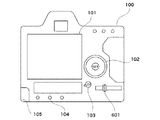
図1は、本発明の一実施の形態に係る入力装置を備える電子機器の背面図である。本入力装置が適用される電子機器としてデジタルカメラ等の撮像装置100を例示するが、本入力装置は、これに限られず、各種の電子機器に適用が可能である。また、入力装置としては、回転操作式の回転操作部102とスライダ操作式のスライダ601の2つを例示するが、これらの入力装置のいずれか1つが備えられるとしてもよい。このほか撮像装置100には、表示部101、電源スイッチ103、操作ボタン104、電池部105等が具備されている。
FIG. 1 is a rear view of an electronic apparatus including an input device according to an embodiment of the present invention. The
回転操作部102、操作ボタン104及びスライダ601は、撮像装置100の操作を指示する操作部材である。本実施の形態では、回転操作部102及びスライダ601に、静電容量方式のセンサを適用する。まず、回転操作部102に適用した場合の構成について説明する。
The
表示部101は、LCD等により構成され、撮像装置100の内部状態に応じて、文字、画像等を用いて動作状態やメッセージ等を表示する。電源スイッチ103は、撮像装置100の電源をON/OFFするスイッチである。電源スイッチ103をOFFにすると、例えば回転操作部102、操作ボタン104、スライダ601等を無効にすることができ、これにより、撮像装置100は低消費電力状態となる。電池部105は、撮像装置100の電源部であり、アルカリ電池やリチウム電池等の一次電池や、NiCd電池、NiMH電池、Li電池等の二次電池、あるいはACアダプター等から構成される。
The
図2は、静電容量方式のタッチセンサについて説明するための模式図である。 FIG. 2 is a schematic diagram for explaining a capacitive touch sensor.
静電容量方式のタッチセンサには、複数の検出方法が考案されているが、図2では、人体の対地静電容量を検出する方法について説明する。図2(a)は、静電容量方式のタッチセンサの構成を簡略的に示している。静電容量方式のタッチセンサIC200にはセンサパターン201が接続されており、センサパターン201には所定のタイミングで電圧が印加される。人の指202は対地静電容量を持つため、人の指202がセンサパターン201に接触している場合と接触していない場合とで、センサパターン201上に蓄えられる電荷量に差が生じる。その電荷量の差をセンサIC200にて検出することで、人の指202が接触したか否かを判断することができる。センサIC200が検出できるのは人の指202だけに限定されず、対地静電容量の変化を任意に検出することができる。
A plurality of detection methods have been devised for the capacitive touch sensor, but FIG. 2 illustrates a method for detecting the ground capacitance of the human body. FIG. 2A shows a simplified configuration of a capacitive touch sensor. A
そこで、図2(b)のように、センサパターン201と隣接してグランドパターン203を配置することで、センサパターン201とグランドパターン203の上部に対向して金属等の導電部材204があるか否かを検出することができる。図2(b)に示すような構成は、等価的に(概念的に)図2(c)に示すようなコンデンサの直列回路として捉えることができる。すなわち、センサパターン201と導電部材204とが対向する面においてコンデンサ205が構成され、導電部材204とグランドパターン203とが対向する面においてコンデンサ206が構成される。
Therefore, as shown in FIG. 2B, by arranging the
ここで、コンデンサ205の容量をC1とし、コンデンサ205の各電極の平行平面が対向する面積をS1、平行平面の距離をd1、平行平面の間の物質の誘電率をε1とすると、コンデンサ205の容量C1は下記数式1で表される。
[数1]
C1=ε1・S1/d1
同様に、コンデンサ206の容量をC2とし、コンデンサ206の各電極の平行平面が対向する面積をS2、平行平面の距離をd2、平行平面の間の物質の誘電率をε2とすると、コンデンサ205の容量C2は下記数式2で表される。
[数2]
C2=ε2・S2/d2
また、センサIC200が検出する容量Ctotalは、上記数式1、2で表される容量のコンデンサの直列接続における容量であるから、下記数式3のように表される。
[数3]
Ctotal=C1・C2/(C1+C2)
=ε1・ε2・S1・S2/(ε1・d2・S1+ε2・d1・S2)
上記数式3において、簡略的にd1=d2、ε1=ε2とすると、容量Ctotalは下記数式4により表される。
[数4]
Ctotal=ε1・S1・S2/d1(S1+S2)
上記数式4から、S1=S2となるとき、容量Ctotalが最大となることがわかり、そのときの容量Ctotalは下記数式5により表される。
[数5]
Ctotal=ε1・S1/(2・d1)
このような考え方に基づけば、回転操作部102やスライダ601に静電容量方式のタッチセンサを適用する場合において、容量Ctotalに相当するものを最大化し、検出感度を高めることが可能となる。まず、回転操作部102に関して説明する。
Here, assuming that the capacitance of the
[Equation 1]
C1 = ε1 · S1 / d1
Similarly, assuming that the capacitance of the
[Equation 2]
C2 = ε2 / S2 / d2
Further, the capacitance Ctotal detected by the
[Equation 3]
Ctotal = C1 / C2 / (C1 + C2)
= Ε1, ε2, S1, S2 / (ε1, d2, S1 + ε2, d1, S2)
In
[Equation 4]
Ctotal = ε1, S1, S2 / d1 (S1 + S2)
From the above formula 4, it can be seen that the capacity Ctotal is maximized when S1 = S2, and the capacity Ctotal at that time is expressed by the following formula 5.
[Equation 5]
Ctotal = ε1 · S1 / (2 · d1)
Based on such a concept, when a capacitive touch sensor is applied to the
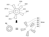
図3は、回転操作部102の構成を模式的に示す図である。回転操作部102は、主に操作部材300、導電部材310、クリック部(クリック手段)301、基板303、固定部307を備える。固定部307は撮像装置100に固定されている。以降、撮像装置100(図1)の背面から見た方向を回転操作部102の正面視とする。図3では、上から順に、回転操作部102の断面図、操作部材300の正面図、クリック部301及び操作部材300の正面図、導電部材310の正面図、基板303の正面図を示す。
FIG. 3 is a diagram schematically illustrating the configuration of the
操作部材300はユーザが直接触れて操作する環状の部材であり、回転中心Cを中心として、固定部307に対して回転自在となっている。操作部材300の半径方向中心位置には、セットボタン304が配置されている。セットボタン304は、例えば、操作部材300を所望の位置に回転させて操作を決定するために使用される。セットボタン304は操作部材300、導電部材310、基板303を貫通して配置される。セットボタン304を押圧することで、固定部307に配置されるプッシュスイッチをオンする。
The
操作部材300の外周部には、バネ306を介してボール305が、操作部材300の半径方向外側に少し突出するように設けられる。バネ306及びボール305は操作部材300と一緒に回転する。バネ306の弾性によって、ボール305は操作部材300の半径方向に移動可能である。
A
クリック部301は、固定部307に対して固定され、操作部材300の回転によらず固定状態を維持する。クリック部301は環状に形成され、内周側に凹部301a及び凸部301bの繰り返しでなる凹凸構造を有する。操作部材300が回転するとき、凹部301aにボール305が弾性的に嵌入され、その位置で一応の安定状態となる。ボール305がバネ306の反発力に抗して凸部301bを超えて隣接する凹部301aに移動して嵌まることで、クリック力を生じさせることができる。凹部301aの数(20個)が、1回転当たりのクリック数となる。ただし、操作部材300にクリック力を付与するための構造は、この例示した構造に限定されるものではない。
The
導電部材310は、金属等の導電性を有する材料で形成され、操作部材300と一体に回転中心Cを中心として、固定部307に対して回転するように配設される。導電部材310には、セットボタン304の周りに環状のグランド対向部311が形成される。グランド対向部311は第1の部分に相当する。グランド対向部311の穴311aにセットボタン304が貫通している。グランド対向部311から、複数(5枚)の羽根状のセンサ対向部(第2の部分)312が放射状に延設されている。センサ対向部312は第2の部分に相当する。センサ対向部312は、回転中心Cを中心とする円周方向に等間隔に同一形状で設けられる。操作部材300及び導電部材310の可動方向は回転中心Cを中心とした回転方向である。
The
図4は、基板303のレイアウト例を示す図である。基板303は固定部307に固定される。セットボタン304が基板303の中心部分に配置される関係から、基板303はドーナツ型の形状をしている。しかし、基板303はこの形状に限定する必要はない。基板303は、グランドパターン308及びセンサパターン309が配設されたプリント基板である。基板303の内周部分にグランドパターン308が配置され、グランドパターン308の外側で基板303の外周部分にセンサパターン309が配置される。グランドパターン308は接地された接地電極である。
FIG. 4 is a diagram illustrating a layout example of the
ここで、本実施の形態における導電部材310、グランドパターン308及びセンサパターン309は、図2で示した導電部材204、グランドパターン203及びセンサパターン201に相当する。
Here, the
図3、図4に示すように、グランドパターン308は、導電部材310のグランド対向部311に対応し、回転中心Cを中心とした環状形状である。センサパターン309は、4種類の検出電極309a、309b、309c、309dからなり、該4種類の検出電極は360°の範囲で等間隔に5回繰り返して配置される。したがって、検出電極309a、309b、309c、309dは、それぞれ周方向に309aから309dの順に72°毎に配置される。ここで異種類の検出電極といっても、接続される端子や出力される信号が互いに異なるという意味であり、構成自体は共通である。つまり、各種類の検出電極309a、309b、309c、309dは、基板303と導電部材310との位置関係が変化する方向にそれぞれ複数個形成されている。ここで、検出電極309aが第1の検出電極に相当し、検出電極309bが第2の検出電極に相当し、検出電極309cが第3の検出電極に相当する。
As shown in FIGS. 3 and 4, the
各種類において、検出電極の配列間隔は等角度間隔であって、センサ対向部312の配列間隔と一致している。従って、センサ対向部312は、回転位置によっては、5枚全てが、ある同一種類の5つの検出電極(例えば、検出電極309a)に同時に覆い被さることになる。図3では、5つの検出電極309cに5枚のセンサ対向部312が対向している。したがって、センサ対向部312は、検出電極309a、309b、309c、309dの1つの検出電極が360°の範囲で配置される数と同じ数(本実施形態では、5つ)だけ形成される。ところで、クリック部301における凹部301aの数及び配列間隔は、センサパターン309の検出電極の数及び配列間隔と一致しており、検出電極の位置が20個の凹凸に1対1に対応している。これにより、回転操作における操作感覚に操作の検出が対応している。すなわち、各種類の検出電極309a、309b、309c、309dのいずれかと5枚のセンサ対向部312との対向面積が最大となるときに、操作部材300を保持するクリック力を操作部材300に与えている。
In each type, the arrangement interval of the detection electrodes is an equiangular interval and coincides with the arrangement interval of the
センサ対向部312はセンサパターン309に対して平行に対面し、グランド対向部311はグランドパターン308に対して平行に対面する。これら対面する平行平面間の距離は均一であり、平行平面の間の物質の誘電率も共通とする。
The
図4に示すように、センサパターン309の各検出電極は、基板303上で結線され、センサIC(図示しないが、図2のセンサIC200に相当する)に接続される。4種類の検出電極309a、309b、309c、309dは、それぞれ異なる端子を介してセンサICに接続される。
As shown in FIG. 4, each detection electrode of the
導電部材310が基板303上のグランドパターン308とセンサパターン309に覆い被さって回転することで、操作部材300、ひいては回転操作部102の回転操作を検出することができる。導電部材310が操作部材300と共に回転するとき、グランド対向部311はグランドパターン308に常時対向し、その対向面積はほとんど変化しない。そのため、グランド対向部311とグランドパターン308との間の静電容量はほぼ一定に維持される。
By rotating the
一方、導電部材310が回転するとき、センサ対向部312は、対向する相手となるセンサパターン309(の検出電極)が刻々と変化し、ある種類の検出電極に着目すれば、全く対向しない状況とほぼ全面で対向する状況とが生じ得る。すなわち、センサ対向部312と、ある種類の検出電極との間の静電容量は、導電部材310の回転位置によって変化する。そして、この静電容量の変化に基づいて操作部材300の回転動作がセンサICによって検出される。また、検出電極の種類が3種類以上であって、両側に隣接する検出電極の種類は互いに異なり且ついずれも既知であるので、静電容量の変化が生じた順番から、操作部材300の回転方向も把握することができる。
On the other hand, when the
図5は、導電部材310がグランドパターン308及びセンサパターン309に対して対向する面積を説明するための図である。
FIG. 5 is a diagram for explaining an area where the
上記したように、導電部材310のグランド対向部311がグランドパターン308と対向し、その対向面積SGは、導電部材310の回転角度にかかわらず、ほぼ一定である。導電部材310のセンサ対向部312がセンサパターン309と対向する面積は、導電部材310の回転角度によって変化する。例えば、5つの検出電極309aに5枚のセンサ対向部312の回転位置が一致し、同時に対向したときに対向面積が最大となる。1つのセンサ対向部312の、1つの検出電極に対する対向面積の最大値をSSとする。
As described above, the
導電部材310のうち、同一種類の検出電極に対して対向する領域の総面積が最大となるとき、その総面積の最大値を最大面積Smaxとする。最大面積Smaxは、最大値SSの5倍である。このことは、いずれの種類の検出電極(309a〜309d)についても同様である。
When the total area of the regions facing the same type of detection electrode in the
本実施の形態では、最大面積Smaxは、導電部材310がグランドパターン308と対向する上記の対向面積SGと略等しくなるように設定されている。最も好ましくは両者を一致させる。これは、図2の一般例でいえば、S1=S2とすることに相当する。これにより、導電部材310とセンサパターン309との間の静電容量の変化の検出レベルが最大になる(最適化される)。すなわち、静電容量方式のセンサの検出レベルを最適化(最大化)するためのセンサパターンの構成となっており、検出の感度が高まる。
In the present embodiment, the maximum area Smax is set so as to be substantially equal to the facing area SG where the
本実施の形態によれば、操作部材300の可動行程において、導電部材310のうちセンサパターン309に対向する領域の総面積が変化する。そして、それが最大となるときの最大面積Smaxは、導電部材310のうちグランドパターン308に対向する領域の面積(対向面積SG)と略等しい。これにより、回転操作部102が小型化されてセンサパターン309が小さくなっても、効率的に検出レベルを得ることができ、静電容量方式のセンサのセンサパターンを最適に構成することができる。よって、静電容量方式の操作検出における検出感度を高めることができる。
According to the present embodiment, the total area of the region of the
また、センサパターン309には複数種類の検出電極があり、同一種類の全ての検出電極に対して導電部材310の全てのセンサ対向部312が同時に対向するので、検出感度を高く維持しつつ分解能を高めることができる。
Further, the
また、操作部材300の可動方向においてセンサパターン309の検出電極の配置位置が、クリック部301における凹凸によるクリック感の発生位置と対応しているので、操作感覚と操作検出とを対応させることができる。
Moreover, since the arrangement position of the detection electrode of the
ところで、基板303のレイアウトは例示したものに限定されるものではない。本実施の形態では、基板303の内周側にグランドパターン308、外周側にセンサパターン309を配置したが、これとは逆にしてもよい。つまり、基板303の外周側に大きな環状のグランドパターン308を1つ設け、グランドパターン308の内側にセンサパターン309の複数の検出電極を円周方向に配列するようにしてもよい。
By the way, the layout of the
また、本実施の形態では、クリック数を20個とすると共に、センサパターン309の検出電極を4種類(a、b、c、d)とし、総センサパターン数を20個としたが、この数に限られない。特に、検出電極の種類は3種類以上であれば、回転方向の検出が可能である。
In this embodiment, the number of clicks is set to 20, the number of detection electrodes of the
また、図6に変形例を示すように、検出電極の種類を2種類とする構成も考えられる。図6は、変形例の基板303のレイアウトを示す図である。
Further, as shown in FIG. 6, a configuration in which two types of detection electrodes are used is also conceivable. FIG. 6 is a diagram showing a layout of a
この変形例では、図4に示すレイアウトに対して、センサパターン309に代えて、2種類のセンサパターン321、322を設ける。基板303の半径方向において、センサパターン322は、グランドパターン308の外側に配置され、センサパターン321は、センサパターン322の外側に配置される。すなわち、基板303と導電部材310との位置関係が変化する方向と直交する方向で、センサパターン321の検出電極とセンサパターン322の検出電極とが千鳥配置となるように形成される。センサパターン321の検出電極が第1の検出電極に相当し、センサパターン322の検出電極が第2の検出電極に相当する。
In this modification, two types of
センサパターン321、322はそれぞれ、円周方向に沿って一定の間隔を開けて間欠的に5個ずつ(e、f)配列される。ただし、円周方向における配置位置が、センサパターン321とセンサパターン322とでずれていて、位相が半周期ずれた、いわゆる千鳥配置となっている。
Each of the
この場合、円周方向においてセンサパターン321、322のいずれかの端が位置する箇所が20箇所ある。従って、20の分解能で検出が可能である。20個のクリック数に対し、総センサパターン数は10個で構成できる。このように、2種類の検出電極が操作部材300の可動方向に千鳥配置されることで、2種類の検出電極にて分解能を高めることができる。
In this case, there are 20 places where any one end of the
次に、スライダ601に、静電容量方式のセンサを適用した場合の構成について図7、図8を用いて説明する。
Next, a configuration when a capacitive sensor is applied to the
図7は、スライダ601の構成を模式的に示す図である。スライダ601は、スライダ式の操作部材である。図7では、デジタル的に検出値が変化する構成を例示し、アナログ的検出値が変化する構成については図8で後述する。デジタル的に値を変化させる用途として、例えば、電源のON/OFF切り替え、カメラモードの切り替え、他の操作部材のON/OFF切り替え等の操作が考えられる。アナログ的に値を変化させる用途として、例えば、動画再生時のスピーカの音量調節や、動画記録時のマイクの音量調節、表示部101の輝度調整、撮影時のパラメータ(色温度等)の調整等の操作が考えられる。
FIG. 7 is a diagram schematically showing the configuration of the
図7に示すように、スライダ601は、回転操作部102における操作部材300、導電部材310、クリック部301、基板303(図3参照)に相当するものとして、操作部材700、導電部材706、クリック部702、基板707を主に備える。図7(a)、(b)、(c)は、それぞれ、スライダ601の断面図、クリック部702の正面図、基板707の正面図である。
As shown in FIG. 7, the
操作部材700は、ユーザが直接触れて操作する部材であり、撮像装置100の筐体の一部701に対して図7(a)の左右方向に直線的にスライド自在となっている。導電部材706は、金属等の導電性部材で構成され、操作部材700と一体にスライド移動する。クリック部702は、筐体の一部701に対して固定され、操作部材700の移動によらず固定状態を維持する。
The
操作部材700には、一体にスライド移動する連動部703が設けられる。図7(b)に示すように、連動部703は、回転操作部102(図3)におけるバネ306及びボール305に相当するバネ705及びボール704を有する。また、クリック部702は、回転操作部102における凹部301a及び凸部301bに相当する凹部702a及び凸部702bの繰り返しでなる凹凸構造を有する。この凹凸構造の形成方向は操作部材700の可動方向と同じ直線方向である。
The
回転操作部102と同様に、ボール704がバネ705の反発力に抗して凸部702bを超えて隣接する凹部702aに移動して嵌まることで、1クリック分のクリック感を生じさせることができる。ただし、操作部材700の回転操作に対してクリック感を付与するための構造は、この例示した構造に限定されるものではない。
Similarly to the
図7(c)に示すように、基板707は、グランドパターン709及びセンサパターン708が配設されたプリント基板である。センサパターン708は、複数(10種類)の方形の検出電極(a〜j)が操作部材700の可動方向に一列に配列されてなる。検出電極(a〜j)は、いずれも大きさや形状が均一であるが、接続される端子や出力ラインは各々異なる。グランドパターン709は、操作部材700の可動方向における検出電極(a〜j)の配設領域の全域、すなわち、操作部材700の可動範囲の全域に亘って1つ配設される。導電部材706と基板707とは非接触構造となっており、導電部材706は、グランドパターン709及びセンサパターン708に対して平行に対面する。
As shown in FIG. 7C, the
クリック部702における凹凸は、センサパターン708の検出電極の数(10個)及び配列間隔と一致している。導電部材706の領域のうち、グランドパターン709に対向する領域が、導電部材310のグランド対向部311に相当し、センサパターン708に対向する領域が、センサ対向部312に相当する(図3参照)。
The unevenness in the
導電部材706と、センサパターン708における、ある種類の検出電極との間の静電容量は、導電部材706のスライド位置によって変化する。そして、この静電容量の変化に基づいて操作部材700の移動動作がセンサICによって検出される。また、検出電極の種類が3種類以上であって、両側に隣接する検出電極の種類は互いに異なり且ついずれも既知であるので、静電容量の変化が生じた順番から、操作部材700のスライド移動の方向も把握することができる。その他の部分の基本的な構成は回転操作部102と同様である。
The capacitance between the
操作部材700の可動行程において、導電部材706とグランドパターン709との対向面積SGは一定である。一方、導電部材706の移動方向における位置がセンサパターン708のいずれかの検出電極の位置に一致したとき、導電部材706とセンサパターン708との対向面積が最大となる。このように導電部材706のうちセンサパターン708に対して対向する領域の総面積が最大となるとき、その最大面積Smaxは、対向面積SGと略等しくなるように設定されている。
In the movable stroke of the
図8は、アナログ的に値を変化させるスライダ601の構成を模式的に示す図である。図8(a)、(b)に示すスライダ601は、図7に示すスライダ601に対して、クリック部702及び連動部703を廃止した点と、基板707に配設したセンサパターンの形状を変えた点が異なり、その他の構成は同様である。図8(a)、(b)は、それぞれ、スライダ601の断面図、基板707の正面図を示す。
FIG. 8 is a diagram schematically showing the configuration of the
図8(b)に示すように、基板707には、図7の例に対して、センサパターン708に代えてセンサパターン803が配設される。センサパターン803は、複数(10種類)の検出電極(a〜j)が操作部材700の可動方向に一列に配列されてなる。検出電極(a〜j)は、平行四辺形であり、隣接するもの同士が、操作部材700の可動方向においてオーバーラップするように構成されている。
As shown in FIG. 8B, a
センサパターン803の各検出電極から得られる検出レベルは、操作部材700をスライドさせることでアナログ的に変化する。これにより、操作部材700の移動方向や、どの位置にいるかを検出することができる。
The detection level obtained from each detection electrode of the
操作部材700の可動行程において、導電部材706とグランドパターン709との対向面積SGは一定である。一方、センサパターン803の検出電極の形状や隙間とも関係するが、導電部材706のうちセンサパターン803に対して対向する領域の総面積が最大となるとき、それを最大面積Smaxとする。図8(a)、(b)に示す例に限れば、導電部材706のいずれの位置においても、センサパターン803との対向面積が一定で且つ最大でもある。最大面積Smaxは、対向面積SGと略等しくなるように設定されている。
In the movable stroke of the
図7、図8に示す構成のように、操作部材700の可動方向が直線的なスライダ601についても、静電容量方式の操作検出における検出感度を高めることができる。
As in the configurations shown in FIGS. 7 and 8, the detection sensitivity in the capacitive type operation detection can be increased even for the
なお、図7、図8に示す例において、操作部材700の移動方向を検出可能にする観点からは、センサパターン708、803の検出電極は最低3種類とし、操作部材700の可動方向に決まった順番で配列すればよい。また、導電部材706については、導電部材310のセンサ対向部312(図4)と同じように、同一種類の検出電極に同時に対向するような複数のセンサ対向部を設けてもよい。
In the example shown in FIGS. 7 and 8, from the viewpoint of making it possible to detect the moving direction of the
なお、図6で示したような基板レイアウトを、図7または図8の例に適用し、直線方向に沿ってセンサパターンの2種類の検出電極を千鳥配置してもよい。 Note that the substrate layout as shown in FIG. 6 may be applied to the example of FIG. 7 or FIG. 8, and two types of detection electrodes of the sensor pattern may be staggered along the linear direction.
なお、上述した各種の例では、操作部材(300、700)の可動方向は回転方向、直線方向であったが、これらに限られない。操作部材が、湾曲した弧状等、非直線的な経路を往復または1周するように構成し、その可動方向に沿ってセンサパターンの検出電極を複数配列してもよい。また、操作部材の操作方向は押し引き方向であってもよい。 In the various examples described above, the movable direction of the operation member (300, 700) is the rotational direction or the linear direction, but is not limited thereto. The operation member may be configured to reciprocate or make one round of a non-linear path such as a curved arc, and a plurality of detection electrodes of the sensor pattern may be arranged along the movable direction. Further, the operation direction of the operation member may be a push-pull direction.
なお、上述した各種の例では、操作部材300、700が可動で基板303、基板707が固定であったが、操作部材300、700が基板303、基板707に対して相対的に変位するように構成されていればよい。
In the various examples described above, the
以上、本発明をその好適な実施形態に基づいて詳述してきたが、本発明はこれら特定の実施形態に限られるものではなく、この発明の要旨を逸脱しない範囲の様々な形態も本発明に含まれる。上述の実施形態の一部を適宜組み合わせてもよい。 Although the present invention has been described in detail based on preferred embodiments thereof, the present invention is not limited to these specific embodiments, and various forms within the scope of the present invention are also included in the present invention. included. A part of the above-described embodiments may be appropriately combined.
102 回転操作部
300、700 操作部材
301、702 クリック部
303、707 基板
308、709 グランドパターン
309、321、322、708、803 センサパターン
310、706 導電部材
312 センサ対向部
601 スライダ
102
Claims (6)
導電性を有する材料で形成されている導電部材と、
操作されることで前記基板と前記導電部材との位置関係を変化させる操作部材と、を有し、
前記基板には、前記基板と前記導電部材との位置関係が変化する方向に前記検出電極が複数個形成されており、
前記導電部材には、前記基板と前記導電部材との位置関係が変化しても、前記接地電極と対向する対向面積が変化しない第1の部分が形成されているとともに、前記基板と前記導電部材との位置関係が変化することで、前記検出電極と対向する対向面積が変化する第2の部分が前記基板と前記導電部材との位置関係が変化する方向に前記検出電極と同じ数だけ形成されており、
前記検出電極と前記第2の部分との前記対向面積が最大となるときに、前記検出電極と前記第2の部分との前記対向面積が、前記接地電極と前記第1の部分との前記対向面積と略等しくなるように、前記基板または前記導電部材が形成されていることを特徴とする入力装置。 A substrate Ru Tei and the detection electrode and the ground electrode are formed,
And Tei Rushirubeden member is formed of a conductive material,
It has an operating member for changing the positional relationship between the conductive member and the substrate by being operated, and
A plurality of the detection electrodes are formed on the substrate in a direction in which the positional relationship between the substrate and the conductive member changes,
Wherein the conductive member, even if the positional relationship between the conductive member and the substrate is changed, the first portion being formed Rutotomoni the facing area facing the ground electrode does not change, the substrate and the conductive member As a result of the change in the positional relationship between the substrate and the conductive member, the same number of second portions as the detection electrode are formed in the direction in which the positional relationship between the substrate and the conductive member changes. And
When the facing area between the detection electrode and the second portion is maximized, the facing area between the detection electrode and the second portion is equal to the facing between the ground electrode and the first portion. as becomes substantially equal to the area, the input device comprising that you have formed the substrate or the conductive member.
導電性を有する材料で形成されている導電部材と、
操作されることで前記基板と前記導電部材との位置関係を変化させる操作部材と、を有し、
前記基板には、前記基板と前記導電部材との位置関係が変化する方向に、前記第1ないし第3の検出電極が並べて形成されており、
前記導電部材には、前記基板と前記導電部材との位置関係が変化しても、前記接地電極と対向する対向面積が変化しない第1の部分が形成されているとともに、前記基板と前記導電部材との位置関係が変化することで、前記第1ないし第3の検出電極のいずれか1つと対向する対向面積が変化する第2の部分が形成されており、
前記第1ないし第3の検出電極のいずれか1つと前記第2の部分との前記対向面積が最大となるときに、前記第1ないし第3の検出電極のいずれか1つと前記第2の部分との前記対向面積が、前記接地電極と前記第1の部分との前記対向面積と略等しくなるように、前記基板または前記導電部材が形成されていることを特徴とする入力装置。 A substrate on which first to third detection electrodes for outputting different signals and a ground electrode are formed;
A conductive member formed of a conductive material;
An operation member that is operated to change a positional relationship between the substrate and the conductive member;
In the substrate, the first to third detection electrodes are formed side by side in a direction in which the positional relationship between the substrate and the conductive member changes,
The conductive member is formed with a first portion in which a facing area facing the ground electrode does not change even if a positional relationship between the substrate and the conductive member changes, and the substrate and the conductive member And the second portion where the facing area that faces any one of the first to third detection electrodes changes is formed.
Any one of the first to third detection electrodes and the second portion when the facing area between any one of the first to third detection electrodes and the second portion is maximized. The input device is characterized in that the substrate or the conductive member is formed such that the facing area between the ground electrode and the first portion is substantially equal to the facing area .
導電性を有する材料で形成されている導電部材と、
操作されることで前記基板と前記導電部材との位置関係を変化させる操作部材と、を有し、
前記基板には、前記基板と前記導電部材との位置関係が変化する方向と直交する方向で、前記第1の検出電極と前記第2の検出電極とが千鳥配置となるように形成されており、
前記導電部材には、前記基板と前記導電部材との位置関係が変化しても、前記接地電極と対向する対向面積が変化しない第1の部分が形成されているとともに、前記基板と前記導電部材との位置関係が変化することで、前記第1および第2の検出電極の少なくとも1つと対向する対向面積が変化する第2の部分が形成されており、
前記第1および第2の検出電極の少なくとも1つと前記第2の部分との前記対向面積が最大となるときに、前記第1および第2の検出電極の少なくとも1つと前記第2の部分との前記対向面積が、前記接地電極と前記第1の部分との前記対向面積と略等しくなるように、前記基板または前記導電部材が形成されていることを特徴とする入力装置。 A substrate on which first and second detection electrodes that output different signals and a ground electrode are formed;
A conductive member formed of a conductive material;
An operation member that is operated to change a positional relationship between the substrate and the conductive member;
The substrate is formed so that the first detection electrodes and the second detection electrodes are arranged in a staggered manner in a direction orthogonal to the direction in which the positional relationship between the substrate and the conductive member changes. ,
The conductive member is formed with a first portion in which a facing area facing the ground electrode does not change even if a positional relationship between the substrate and the conductive member changes, and the substrate and the conductive member And the second portion in which the facing area that faces at least one of the first and second detection electrodes is changed is formed.
When the facing area between at least one of the first and second detection electrodes and the second portion is maximized, the at least one of the first and second detection electrodes and the second portion The input device , wherein the substrate or the conductive member is formed so that the facing area is substantially equal to the facing area between the ground electrode and the first portion .
前記導電部材には、前記基板と前記導電部材との位置関係が変化する方向に前記第2の部分が前記第1の検出電極と同じ数だけ形成されていることを特徴とする請求項2または3に記載の入力装置。 In the substrate, a plurality of the first detection electrodes are formed in a direction in which the positional relationship between the substrate and the conductive member changes, and in a direction in which the positional relationship between the substrate and the conductive member changes. The same number of the second detection electrodes as the first detection electrodes are formed,
3. The conductive member is formed with the same number of the second portions as the first detection electrodes in the direction in which the positional relationship between the substrate and the conductive member changes. 3. The input device according to 3 .
前記クリック手段は、前記検出電極と前記第2の部分との前記対向面積が最大となるときに、前記操作部材を保持するクリック力を前記操作部材に与えることを特徴とする請求項1ないし4のいずれか1項に記載の入力装置。 A click means for applying a click force to the operation member;
5. The click means applies a click force for holding the operation member to the operation member when the facing area between the detection electrode and the second portion is maximized. The input device according to any one of the above.
Priority Applications (3)
| Application Number | Priority Date | Filing Date | Title |
|---|---|---|---|
| JP2011052883A JP5713733B2 (en) | 2011-03-10 | 2011-03-10 | Input device and electronic device |
| US13/416,118 US8823679B2 (en) | 2011-03-10 | 2012-03-09 | Input apparatus and electronic equipment using capacitive sensing method in detecting operations |
| CN201210061972.2A CN102681692B (en) | 2011-03-10 | 2012-03-09 | Input apparatus and electronic equipment using capacitive sensing method in detecting operations |
Applications Claiming Priority (1)
| Application Number | Priority Date | Filing Date | Title |
|---|---|---|---|
| JP2011052883A JP5713733B2 (en) | 2011-03-10 | 2011-03-10 | Input device and electronic device |
Publications (3)
| Publication Number | Publication Date |
|---|---|
| JP2012190234A JP2012190234A (en) | 2012-10-04 |
| JP2012190234A5 JP2012190234A5 (en) | 2014-04-17 |
| JP5713733B2 true JP5713733B2 (en) | 2015-05-07 |
Family
ID=46794959
Family Applications (1)
| Application Number | Title | Priority Date | Filing Date |
|---|---|---|---|
| JP2011052883A Expired - Fee Related JP5713733B2 (en) | 2011-03-10 | 2011-03-10 | Input device and electronic device |
Country Status (3)
| Country | Link |
|---|---|
| US (1) | US8823679B2 (en) |
| JP (1) | JP5713733B2 (en) |
| CN (1) | CN102681692B (en) |
Families Citing this family (9)
| Publication number | Priority date | Publication date | Assignee | Title |
|---|---|---|---|---|
| JP2016530661A (en) * | 2013-09-17 | 2016-09-29 | サーク・コーポレーション | Projector electrodes extend the sensitivity range of proximity sensors |
| CN105556439A (en) | 2013-09-20 | 2016-05-04 | 株式会社村田制作所 | Detection sensor and input device |
| JP6381381B2 (en) | 2014-09-12 | 2018-08-29 | キヤノン株式会社 | Electronics |
| EP3220402B1 (en) * | 2014-11-10 | 2020-03-11 | Panasonic Intellectual Property Management Co., Ltd. | Input device |
| EP3037898B1 (en) * | 2014-12-23 | 2017-06-21 | ETA SA Manufacture Horlogère Suisse | Electromechanical apparatus comprising a device for capacitive detection of the angular position of a moving element, and method for detecting the angular position of a moving element |
| EP3438765B1 (en) * | 2017-08-04 | 2020-02-05 | ETA SA Manufacture Horlogère Suisse | Horological movement comprising a device for detecting an angular position of a wheel |
| JP7033747B2 (en) * | 2018-02-21 | 2022-03-11 | パナソニックIpマネジメント株式会社 | Displacement detection device and operation device equipped with this |
| JP6465327B1 (en) * | 2018-03-06 | 2019-02-06 | セイコーインスツル株式会社 | clock |
| DE102019114429A1 (en) * | 2019-05-29 | 2020-12-03 | Preh Gmbh | Input device with movable handle on a capacitive detection surface and capacitive coupling devices |
Family Cites Families (20)
| Publication number | Priority date | Publication date | Assignee | Title |
|---|---|---|---|---|
| US3961318A (en) * | 1975-01-17 | 1976-06-01 | Inductosyn Corporation | Electrostatic position-measuring transducer |
| US5136286A (en) * | 1990-01-29 | 1992-08-04 | Siecor Corporation | Switched capacitance meter reading device using variable width electrodes |
| JP3235005B2 (en) * | 1993-09-14 | 2001-12-04 | セイコープレシジョン株式会社 | Position detection device |
| JP2001296966A (en) * | 2000-04-17 | 2001-10-26 | Alps Electric Co Ltd | Input device |
| JP2003223275A (en) * | 2001-11-22 | 2003-08-08 | Omron Corp | Input device |
| JP4125931B2 (en) * | 2002-08-26 | 2008-07-30 | 株式会社ワコー | Rotation operation amount input device and operation device using the same |
| WO2005019766A2 (en) * | 2003-08-21 | 2005-03-03 | Harald Philipp | Capacitive position sensor |
| US20070291016A1 (en) * | 2006-06-20 | 2007-12-20 | Harald Philipp | Capacitive Position Sensor |
| JP4899963B2 (en) * | 2007-03-26 | 2012-03-21 | パナソニック株式会社 | Input device and manufacturing method thereof |
| JP2009218785A (en) | 2008-03-10 | 2009-09-24 | Toto Ltd | Electrostatic capacity type operation switch and cock device using the same |
| JP5429636B2 (en) * | 2009-04-10 | 2014-02-26 | Nltテクノロジー株式会社 | Touch sensor device and electronic apparatus equipped with the same |
| CN102576276B (en) * | 2010-08-23 | 2017-05-10 | 谱瑞科技股份有限公司 | Capacitance scanning proximity detection |
| US20120327013A1 (en) * | 2011-06-22 | 2012-12-27 | Lee Jeffery T | Method and apparatus for initiating operations on a touch device |
| JP5843511B2 (en) * | 2011-07-29 | 2016-01-13 | キヤノン株式会社 | INPUT DETECTING DEVICE, ITS CONTROL METHOD, PROGRAM, AND RECORDING MEDIUM |
| US9490804B2 (en) * | 2011-09-28 | 2016-11-08 | Cypress Semiconductor Corporation | Capacitance sensing circuits, methods and systems having conductive touch surface |
| US9372582B2 (en) * | 2012-04-19 | 2016-06-21 | Atmel Corporation | Self-capacitance measurement |
| US10126883B2 (en) * | 2012-07-03 | 2018-11-13 | Sharp Kabushiki Kaisha | Capacitive touch panel with height determination function |
| US9098152B2 (en) * | 2012-07-24 | 2015-08-04 | Atmel Corporation | Dielectric layer for touch sensor stack |
| US9213052B2 (en) * | 2012-08-01 | 2015-12-15 | Parade Technologies, Ltd. | Peak detection schemes for touch position detection |
| US9110545B2 (en) * | 2012-08-16 | 2015-08-18 | Nokia Technologies Oy | Apparatus and associated methods |
-
2011
- 2011-03-10 JP JP2011052883A patent/JP5713733B2/en not_active Expired - Fee Related
-
2012
- 2012-03-09 US US13/416,118 patent/US8823679B2/en not_active Expired - Fee Related
- 2012-03-09 CN CN201210061972.2A patent/CN102681692B/en not_active Expired - Fee Related
Also Published As
| Publication number | Publication date |
|---|---|
| JP2012190234A (en) | 2012-10-04 |
| CN102681692B (en) | 2015-07-22 |
| US8823679B2 (en) | 2014-09-02 |
| US20120229150A1 (en) | 2012-09-13 |
| CN102681692A (en) | 2012-09-19 |
Similar Documents
| Publication | Publication Date | Title |
|---|---|---|
| JP5713733B2 (en) | Input device and electronic device | |
| US9110545B2 (en) | Apparatus and associated methods | |
| US9405421B2 (en) | Mutual capacitance touch sensing device | |
| US9360967B2 (en) | Mutual capacitance touch sensing device | |
| JP2012190234A5 (en) | ||
| US20080078590A1 (en) | Pointing device using capacitance sensor | |
| US20130106758A1 (en) | Apparatus and Associated Methods | |
| TW201005616A (en) | Capacitive touch screen of a display device for detecting finger and stylus | |
| JPWO2002044649A1 (en) | Capacitive sensor | |
| WO2014209718A1 (en) | Haptic display with simultaneous sensing and actuation | |
| JP2009295155A (en) | Input device | |
| JP2012226743A (en) | Touch screen device | |
| JP2004311196A (en) | Input device | |
| JP2024503281A (en) | rotatable knob interface | |
| WO2021140550A1 (en) | Tactile presentation panel, tactile presentation touch panel, and tactile presentation touch display | |
| JP2022075255A (en) | Input detection system and input support device | |
| WO2019017153A1 (en) | Information processing device, information processing method, and program | |
| US10114502B2 (en) | Touch panel comprising touch electrodes in two areas in which a distance between two adjacent touch electrodes in the first area differs from that of the second area | |
| EP2818987B1 (en) | Tablet having flexible and transparent sensing area | |
| US20220253155A1 (en) | Input device and input system | |
| JP3421783B2 (en) | Capacitive sensor | |
| US10754121B2 (en) | Displacement detecting apparatus, lens barrel, and imaging apparatus | |
| JP5227405B2 (en) | Capacitance type motion detection device and input device using the same | |
| KR101776667B1 (en) | Pressure detecting device using frame of a display module | |
| JPH0749325A (en) | Electrostatic capacitance type sensor |
Legal Events
| Date | Code | Title | Description |
|---|---|---|---|
| A521 | Request for written amendment filed |
Free format text: JAPANESE INTERMEDIATE CODE: A523 Effective date: 20140227 |
|
| A621 | Written request for application examination |
Free format text: JAPANESE INTERMEDIATE CODE: A621 Effective date: 20140227 |
|
| A977 | Report on retrieval |
Free format text: JAPANESE INTERMEDIATE CODE: A971007 Effective date: 20140929 |
|
| A131 | Notification of reasons for refusal |
Free format text: JAPANESE INTERMEDIATE CODE: A131 Effective date: 20141028 |
|
| A521 | Request for written amendment filed |
Free format text: JAPANESE INTERMEDIATE CODE: A523 Effective date: 20141217 |
|
| TRDD | Decision of grant or rejection written | ||
| A01 | Written decision to grant a patent or to grant a registration (utility model) |
Free format text: JAPANESE INTERMEDIATE CODE: A01 Effective date: 20150210 |
|
| A61 | First payment of annual fees (during grant procedure) |
Free format text: JAPANESE INTERMEDIATE CODE: A61 Effective date: 20150310 |
|
| R151 | Written notification of patent or utility model registration |
Ref document number: 5713733 Country of ref document: JP Free format text: JAPANESE INTERMEDIATE CODE: R151 |
|
| LAPS | Cancellation because of no payment of annual fees |