JP5707697B2 - Light emitting device - Google Patents
Light emitting device Download PDFInfo
- Publication number
- JP5707697B2 JP5707697B2 JP2009285971A JP2009285971A JP5707697B2 JP 5707697 B2 JP5707697 B2 JP 5707697B2 JP 2009285971 A JP2009285971 A JP 2009285971A JP 2009285971 A JP2009285971 A JP 2009285971A JP 5707697 B2 JP5707697 B2 JP 5707697B2
- Authority
- JP
- Japan
- Prior art keywords
- light emitting
- light
- emitting element
- layer
- semiconductor
- Prior art date
- Legal status (The legal status is an assumption and is not a legal conclusion. Google has not performed a legal analysis and makes no representation as to the accuracy of the status listed.)
- Active
Links
- OAICVXFJPJFONN-UHFFFAOYSA-N Phosphorus Chemical compound [P] OAICVXFJPJFONN-UHFFFAOYSA-N 0.000 claims description 252
- 239000004065 semiconductor Substances 0.000 claims description 238
- 239000002245 particle Substances 0.000 claims description 170
- 239000006185 dispersion Substances 0.000 claims description 6
- 239000010410 layer Substances 0.000 description 308
- 238000009826 distribution Methods 0.000 description 62
- 239000000758 substrate Substances 0.000 description 58
- 239000000463 material Substances 0.000 description 37
- 229920005989 resin Polymers 0.000 description 34
- 239000011347 resin Substances 0.000 description 34
- 238000000605 extraction Methods 0.000 description 31
- 229910010272 inorganic material Inorganic materials 0.000 description 22
- 239000011147 inorganic material Substances 0.000 description 22
- 239000003795 chemical substances by application Substances 0.000 description 18
- 239000011342 resin composition Substances 0.000 description 15
- 229920002050 silicone resin Polymers 0.000 description 13
- 239000012790 adhesive layer Substances 0.000 description 12
- 239000000203 mixture Substances 0.000 description 11
- 230000003287 optical effect Effects 0.000 description 10
- 239000013078 crystal Substances 0.000 description 8
- 230000007423 decrease Effects 0.000 description 8
- 239000003822 epoxy resin Substances 0.000 description 7
- 239000002223 garnet Substances 0.000 description 7
- 239000011521 glass Substances 0.000 description 7
- 238000000034 method Methods 0.000 description 7
- 150000004767 nitrides Chemical class 0.000 description 7
- 229920000647 polyepoxide Polymers 0.000 description 7
- 238000009877 rendering Methods 0.000 description 7
- 229910052684 Cerium Inorganic materials 0.000 description 5
- 229910052693 Europium Inorganic materials 0.000 description 5
- 229910052791 calcium Inorganic materials 0.000 description 5
- 239000000919 ceramic Substances 0.000 description 5
- GWXLDORMOJMVQZ-UHFFFAOYSA-N cerium Chemical compound [Ce] GWXLDORMOJMVQZ-UHFFFAOYSA-N 0.000 description 5
- 239000011368 organic material Substances 0.000 description 5
- 125000001997 phenyl group Chemical group [H]C1=C([H])C([H])=C(*)C([H])=C1[H] 0.000 description 5
- 238000010521 absorption reaction Methods 0.000 description 4
- JNDMLEXHDPKVFC-UHFFFAOYSA-N aluminum;oxygen(2-);yttrium(3+) Chemical compound [O-2].[O-2].[O-2].[Al+3].[Y+3] JNDMLEXHDPKVFC-UHFFFAOYSA-N 0.000 description 4
- 230000017525 heat dissipation Effects 0.000 description 4
- 229910052751 metal Inorganic materials 0.000 description 4
- 239000002184 metal Substances 0.000 description 4
- 238000004382 potting Methods 0.000 description 4
- 229910052712 strontium Inorganic materials 0.000 description 4
- 239000000126 substance Substances 0.000 description 4
- 229910019901 yttrium aluminum garnet Inorganic materials 0.000 description 4
- 239000004925 Acrylic resin Substances 0.000 description 3
- 229920000178 Acrylic resin Polymers 0.000 description 3
- 229910007991 Si-N Inorganic materials 0.000 description 3
- 229910006294 Si—N Inorganic materials 0.000 description 3
- GWEVSGVZZGPLCZ-UHFFFAOYSA-N Titan oxide Chemical compound O=[Ti]=O GWEVSGVZZGPLCZ-UHFFFAOYSA-N 0.000 description 3
- PNEYBMLMFCGWSK-UHFFFAOYSA-N aluminium oxide Inorganic materials [O-2].[O-2].[O-2].[Al+3].[Al+3] PNEYBMLMFCGWSK-UHFFFAOYSA-N 0.000 description 3
- 238000000149 argon plasma sintering Methods 0.000 description 3
- 239000003086 colorant Substances 0.000 description 3
- PMHQVHHXPFUNSP-UHFFFAOYSA-M copper(1+);methylsulfanylmethane;bromide Chemical compound Br[Cu].CSC PMHQVHHXPFUNSP-UHFFFAOYSA-M 0.000 description 3
- 230000000694 effects Effects 0.000 description 3
- 239000000284 extract Substances 0.000 description 3
- 239000010408 film Substances 0.000 description 3
- 238000004519 manufacturing process Methods 0.000 description 3
- 229910052594 sapphire Inorganic materials 0.000 description 3
- 239000010980 sapphire Substances 0.000 description 3
- 229910000679 solder Inorganic materials 0.000 description 3
- 239000010409 thin film Substances 0.000 description 3
- 229910002601 GaN Inorganic materials 0.000 description 2
- BPQQTUXANYXVAA-UHFFFAOYSA-N Orthosilicate Chemical compound [O-][Si]([O-])([O-])[O-] BPQQTUXANYXVAA-UHFFFAOYSA-N 0.000 description 2
- 229910052581 Si3N4 Inorganic materials 0.000 description 2
- 229910004283 SiO 4 Inorganic materials 0.000 description 2
- VYPSYNLAJGMNEJ-UHFFFAOYSA-N Silicium dioxide Chemical compound O=[Si]=O VYPSYNLAJGMNEJ-UHFFFAOYSA-N 0.000 description 2
- 229910006360 Si—O—N Inorganic materials 0.000 description 2
- MCMNRKCIXSYSNV-UHFFFAOYSA-N Zirconium dioxide Chemical compound O=[Zr]=O MCMNRKCIXSYSNV-UHFFFAOYSA-N 0.000 description 2
- 229910052784 alkaline earth metal Inorganic materials 0.000 description 2
- 150000001342 alkaline earth metals Chemical class 0.000 description 2
- 229910052782 aluminium Inorganic materials 0.000 description 2
- XAGFODPZIPBFFR-UHFFFAOYSA-N aluminium Chemical compound [Al] XAGFODPZIPBFFR-UHFFFAOYSA-N 0.000 description 2
- 238000013459 approach Methods 0.000 description 2
- 239000007767 bonding agent Substances 0.000 description 2
- 238000006243 chemical reaction Methods 0.000 description 2
- 238000010586 diagram Methods 0.000 description 2
- 239000010419 fine particle Substances 0.000 description 2
- -1 gallium nitride compound Chemical class 0.000 description 2
- 125000002496 methyl group Chemical group [H]C([H])([H])* 0.000 description 2
- 229910000484 niobium oxide Inorganic materials 0.000 description 2
- URLJKFSTXLNXLG-UHFFFAOYSA-N niobium(5+);oxygen(2-) Chemical compound [O-2].[O-2].[O-2].[O-2].[O-2].[Nb+5].[Nb+5] URLJKFSTXLNXLG-UHFFFAOYSA-N 0.000 description 2
- RVTZCBVAJQQJTK-UHFFFAOYSA-N oxygen(2-);zirconium(4+) Chemical compound [O-2].[O-2].[Zr+4] RVTZCBVAJQQJTK-UHFFFAOYSA-N 0.000 description 2
- BASFCYQUMIYNBI-UHFFFAOYSA-N platinum Chemical compound [Pt] BASFCYQUMIYNBI-UHFFFAOYSA-N 0.000 description 2
- 238000007639 printing Methods 0.000 description 2
- 230000001681 protective effect Effects 0.000 description 2
- 238000007650 screen-printing Methods 0.000 description 2
- HQVNEWCFYHHQES-UHFFFAOYSA-N silicon nitride Chemical compound N12[Si]34N5[Si]62N3[Si]51N64 HQVNEWCFYHHQES-UHFFFAOYSA-N 0.000 description 2
- 238000002834 transmittance Methods 0.000 description 2
- 239000011701 zinc Substances 0.000 description 2
- 229910001928 zirconium oxide Inorganic materials 0.000 description 2
- 229910014458 Ca-Si Inorganic materials 0.000 description 1
- 239000004593 Epoxy Substances 0.000 description 1
- 229910052688 Gadolinium Inorganic materials 0.000 description 1
- 229910000530 Gallium indium arsenide Inorganic materials 0.000 description 1
- 229910052765 Lutetium Inorganic materials 0.000 description 1
- 229910004298 SiO 2 Inorganic materials 0.000 description 1
- UCKMPCXJQFINFW-UHFFFAOYSA-N Sulphide Chemical compound [S-2] UCKMPCXJQFINFW-UHFFFAOYSA-N 0.000 description 1
- 229910052771 Terbium Inorganic materials 0.000 description 1
- 239000005083 Zinc sulfide Substances 0.000 description 1
- 239000006096 absorbing agent Substances 0.000 description 1
- 239000000853 adhesive Substances 0.000 description 1
- 230000001070 adhesive effect Effects 0.000 description 1
- 229910052788 barium Inorganic materials 0.000 description 1
- 229910052793 cadmium Inorganic materials 0.000 description 1
- 229910000420 cerium oxide Inorganic materials 0.000 description 1
- 239000002131 composite material Substances 0.000 description 1
- 229910003460 diamond Inorganic materials 0.000 description 1
- 239000010432 diamond Substances 0.000 description 1
- 238000001962 electrophoresis Methods 0.000 description 1
- 238000005530 etching Methods 0.000 description 1
- 238000005286 illumination Methods 0.000 description 1
- 229910003437 indium oxide Inorganic materials 0.000 description 1
- PJXISJQVUVHSOJ-UHFFFAOYSA-N indium(iii) oxide Chemical compound [O-2].[O-2].[O-2].[In+3].[In+3] PJXISJQVUVHSOJ-UHFFFAOYSA-N 0.000 description 1
- 229910052746 lanthanum Inorganic materials 0.000 description 1
- 238000004020 luminiscence type Methods 0.000 description 1
- TWNQGVIAIRXVLR-UHFFFAOYSA-N oxo(oxoalumanyloxy)alumane Chemical compound O=[Al]O[Al]=O TWNQGVIAIRXVLR-UHFFFAOYSA-N 0.000 description 1
- BMMGVYCKOGBVEV-UHFFFAOYSA-N oxo(oxoceriooxy)cerium Chemical compound [Ce]=O.O=[Ce]=O BMMGVYCKOGBVEV-UHFFFAOYSA-N 0.000 description 1
- SIWVEOZUMHYXCS-UHFFFAOYSA-N oxo(oxoyttriooxy)yttrium Chemical compound O=[Y]O[Y]=O SIWVEOZUMHYXCS-UHFFFAOYSA-N 0.000 description 1
- BPUBBGLMJRNUCC-UHFFFAOYSA-N oxygen(2-);tantalum(5+) Chemical compound [O-2].[O-2].[O-2].[O-2].[O-2].[Ta+5].[Ta+5] BPUBBGLMJRNUCC-UHFFFAOYSA-N 0.000 description 1
- 238000000059 patterning Methods 0.000 description 1
- 229910052697 platinum Inorganic materials 0.000 description 1
- 229920001296 polysiloxane Polymers 0.000 description 1
- 230000005855 radiation Effects 0.000 description 1
- SBIBMFFZSBJNJF-UHFFFAOYSA-N selenium;zinc Chemical compound [Se]=[Zn] SBIBMFFZSBJNJF-UHFFFAOYSA-N 0.000 description 1
- 239000000377 silicon dioxide Substances 0.000 description 1
- 238000000992 sputter etching Methods 0.000 description 1
- 229910001936 tantalum oxide Inorganic materials 0.000 description 1
- OGIDPMRJRNCKJF-UHFFFAOYSA-N titanium oxide Inorganic materials [Ti]=O OGIDPMRJRNCKJF-UHFFFAOYSA-N 0.000 description 1
- QWVYNEUUYROOSZ-UHFFFAOYSA-N trioxido(oxo)vanadium;yttrium(3+) Chemical compound [Y+3].[O-][V]([O-])([O-])=O QWVYNEUUYROOSZ-UHFFFAOYSA-N 0.000 description 1
- 229910052727 yttrium Inorganic materials 0.000 description 1
- 229910052725 zinc Inorganic materials 0.000 description 1
- 229910052984 zinc sulfide Inorganic materials 0.000 description 1
- DRDVZXDWVBGGMH-UHFFFAOYSA-N zinc;sulfide Chemical compound [S-2].[Zn+2] DRDVZXDWVBGGMH-UHFFFAOYSA-N 0.000 description 1
Images


Classifications
-
- H—ELECTRICITY
- H01—ELECTRIC ELEMENTS
- H01L—SEMICONDUCTOR DEVICES NOT COVERED BY CLASS H10
- H01L33/00—Semiconductor devices having potential barriers specially adapted for light emission; Processes or apparatus specially adapted for the manufacture or treatment thereof or of parts thereof; Details thereof
- H01L33/48—Semiconductor devices having potential barriers specially adapted for light emission; Processes or apparatus specially adapted for the manufacture or treatment thereof or of parts thereof; Details thereof characterised by the semiconductor body packages
- H01L33/50—Wavelength conversion elements
- H01L33/501—Wavelength conversion elements characterised by the materials, e.g. binder
- H01L33/502—Wavelength conversion materials
-
- H—ELECTRICITY
- H01—ELECTRIC ELEMENTS
- H01L—SEMICONDUCTOR DEVICES NOT COVERED BY CLASS H10
- H01L33/00—Semiconductor devices having potential barriers specially adapted for light emission; Processes or apparatus specially adapted for the manufacture or treatment thereof or of parts thereof; Details thereof
- H01L33/48—Semiconductor devices having potential barriers specially adapted for light emission; Processes or apparatus specially adapted for the manufacture or treatment thereof or of parts thereof; Details thereof characterised by the semiconductor body packages
- H01L33/50—Wavelength conversion elements
-
- H—ELECTRICITY
- H01—ELECTRIC ELEMENTS
- H01L—SEMICONDUCTOR DEVICES NOT COVERED BY CLASS H10
- H01L2224/00—Indexing scheme for arrangements for connecting or disconnecting semiconductor or solid-state bodies and methods related thereto as covered by H01L24/00
- H01L2224/01—Means for bonding being attached to, or being formed on, the surface to be connected, e.g. chip-to-package, die-attach, "first-level" interconnects; Manufacturing methods related thereto
- H01L2224/10—Bump connectors; Manufacturing methods related thereto
- H01L2224/12—Structure, shape, material or disposition of the bump connectors prior to the connecting process
- H01L2224/13—Structure, shape, material or disposition of the bump connectors prior to the connecting process of an individual bump connector
-
- H—ELECTRICITY
- H01—ELECTRIC ELEMENTS
- H01L—SEMICONDUCTOR DEVICES NOT COVERED BY CLASS H10
- H01L2224/00—Indexing scheme for arrangements for connecting or disconnecting semiconductor or solid-state bodies and methods related thereto as covered by H01L24/00
- H01L2224/01—Means for bonding being attached to, or being formed on, the surface to be connected, e.g. chip-to-package, die-attach, "first-level" interconnects; Manufacturing methods related thereto
- H01L2224/42—Wire connectors; Manufacturing methods related thereto
- H01L2224/47—Structure, shape, material or disposition of the wire connectors after the connecting process
- H01L2224/48—Structure, shape, material or disposition of the wire connectors after the connecting process of an individual wire connector
- H01L2224/4805—Shape
- H01L2224/4809—Loop shape
- H01L2224/48091—Arched
-
- H—ELECTRICITY
- H01—ELECTRIC ELEMENTS
- H01L—SEMICONDUCTOR DEVICES NOT COVERED BY CLASS H10
- H01L2224/00—Indexing scheme for arrangements for connecting or disconnecting semiconductor or solid-state bodies and methods related thereto as covered by H01L24/00
- H01L2224/01—Means for bonding being attached to, or being formed on, the surface to be connected, e.g. chip-to-package, die-attach, "first-level" interconnects; Manufacturing methods related thereto
- H01L2224/42—Wire connectors; Manufacturing methods related thereto
- H01L2224/47—Structure, shape, material or disposition of the wire connectors after the connecting process
- H01L2224/48—Structure, shape, material or disposition of the wire connectors after the connecting process of an individual wire connector
- H01L2224/481—Disposition
- H01L2224/48151—Connecting between a semiconductor or solid-state body and an item not being a semiconductor or solid-state body, e.g. chip-to-substrate, chip-to-passive
- H01L2224/48221—Connecting between a semiconductor or solid-state body and an item not being a semiconductor or solid-state body, e.g. chip-to-substrate, chip-to-passive the body and the item being stacked
- H01L2224/48245—Connecting between a semiconductor or solid-state body and an item not being a semiconductor or solid-state body, e.g. chip-to-substrate, chip-to-passive the body and the item being stacked the item being metallic
- H01L2224/48247—Connecting between a semiconductor or solid-state body and an item not being a semiconductor or solid-state body, e.g. chip-to-substrate, chip-to-passive the body and the item being stacked the item being metallic connecting the wire to a bond pad of the item
-
- H—ELECTRICITY
- H01—ELECTRIC ELEMENTS
- H01L—SEMICONDUCTOR DEVICES NOT COVERED BY CLASS H10
- H01L2224/00—Indexing scheme for arrangements for connecting or disconnecting semiconductor or solid-state bodies and methods related thereto as covered by H01L24/00
- H01L2224/01—Means for bonding being attached to, or being formed on, the surface to be connected, e.g. chip-to-package, die-attach, "first-level" interconnects; Manufacturing methods related thereto
- H01L2224/42—Wire connectors; Manufacturing methods related thereto
- H01L2224/47—Structure, shape, material or disposition of the wire connectors after the connecting process
- H01L2224/48—Structure, shape, material or disposition of the wire connectors after the connecting process of an individual wire connector
- H01L2224/481—Disposition
- H01L2224/48151—Connecting between a semiconductor or solid-state body and an item not being a semiconductor or solid-state body, e.g. chip-to-substrate, chip-to-passive
- H01L2224/48221—Connecting between a semiconductor or solid-state body and an item not being a semiconductor or solid-state body, e.g. chip-to-substrate, chip-to-passive the body and the item being stacked
- H01L2224/48245—Connecting between a semiconductor or solid-state body and an item not being a semiconductor or solid-state body, e.g. chip-to-substrate, chip-to-passive the body and the item being stacked the item being metallic
- H01L2224/48257—Connecting between a semiconductor or solid-state body and an item not being a semiconductor or solid-state body, e.g. chip-to-substrate, chip-to-passive the body and the item being stacked the item being metallic connecting the wire to a die pad of the item
-
- H—ELECTRICITY
- H01—ELECTRIC ELEMENTS
- H01L—SEMICONDUCTOR DEVICES NOT COVERED BY CLASS H10
- H01L2224/00—Indexing scheme for arrangements for connecting or disconnecting semiconductor or solid-state bodies and methods related thereto as covered by H01L24/00
- H01L2224/80—Methods for connecting semiconductor or other solid state bodies using means for bonding being attached to, or being formed on, the surface to be connected
- H01L2224/85—Methods for connecting semiconductor or other solid state bodies using means for bonding being attached to, or being formed on, the surface to be connected using a wire connector
- H01L2224/85909—Post-treatment of the connector or wire bonding area
- H01L2224/8592—Applying permanent coating, e.g. protective coating
-
- H—ELECTRICITY
- H01—ELECTRIC ELEMENTS
- H01L—SEMICONDUCTOR DEVICES NOT COVERED BY CLASS H10
- H01L2924/00—Indexing scheme for arrangements or methods for connecting or disconnecting semiconductor or solid-state bodies as covered by H01L24/00
- H01L2924/15—Details of package parts other than the semiconductor or other solid state devices to be connected
- H01L2924/181—Encapsulation
-
- H—ELECTRICITY
- H01—ELECTRIC ELEMENTS
- H01L—SEMICONDUCTOR DEVICES NOT COVERED BY CLASS H10
- H01L2933/00—Details relating to devices covered by the group H01L33/00 but not provided for in its subgroups
- H01L2933/0091—Scattering means in or on the semiconductor body or semiconductor body package
-
- H—ELECTRICITY
- H01—ELECTRIC ELEMENTS
- H01L—SEMICONDUCTOR DEVICES NOT COVERED BY CLASS H10
- H01L33/00—Semiconductor devices having potential barriers specially adapted for light emission; Processes or apparatus specially adapted for the manufacture or treatment thereof or of parts thereof; Details thereof
- H01L33/48—Semiconductor devices having potential barriers specially adapted for light emission; Processes or apparatus specially adapted for the manufacture or treatment thereof or of parts thereof; Details thereof characterised by the semiconductor body packages
- H01L33/50—Wavelength conversion elements
- H01L33/505—Wavelength conversion elements characterised by the shape, e.g. plate or foil
-
- H—ELECTRICITY
- H01—ELECTRIC ELEMENTS
- H01L—SEMICONDUCTOR DEVICES NOT COVERED BY CLASS H10
- H01L33/00—Semiconductor devices having potential barriers specially adapted for light emission; Processes or apparatus specially adapted for the manufacture or treatment thereof or of parts thereof; Details thereof
- H01L33/48—Semiconductor devices having potential barriers specially adapted for light emission; Processes or apparatus specially adapted for the manufacture or treatment thereof or of parts thereof; Details thereof characterised by the semiconductor body packages
- H01L33/52—Encapsulations
- H01L33/54—Encapsulations having a particular shape
-
- H—ELECTRICITY
- H01—ELECTRIC ELEMENTS
- H01L—SEMICONDUCTOR DEVICES NOT COVERED BY CLASS H10
- H01L33/00—Semiconductor devices having potential barriers specially adapted for light emission; Processes or apparatus specially adapted for the manufacture or treatment thereof or of parts thereof; Details thereof
- H01L33/48—Semiconductor devices having potential barriers specially adapted for light emission; Processes or apparatus specially adapted for the manufacture or treatment thereof or of parts thereof; Details thereof characterised by the semiconductor body packages
- H01L33/64—Heat extraction or cooling elements
- H01L33/644—Heat extraction or cooling elements in intimate contact or integrated with parts of the device other than the semiconductor body
Landscapes
- Engineering & Computer Science (AREA)
- Microelectronics & Electronic Packaging (AREA)
- Manufacturing & Machinery (AREA)
- Computer Hardware Design (AREA)
- Power Engineering (AREA)
- Led Device Packages (AREA)
Description
本発明は、発光素子の発光を一部波長変換してもとの光と混色することにより、異なる色の発光を可能とする発光装置に関する。 The present invention relates to a light-emitting device that enables light emission of different colors by mixing light emitted from a light-emitting element with original light even after wavelength conversion.
発光ダイオード等の半導体発光素子は、小型で電力効率が良く鮮やかな色の発光をする。また、半導体発光素子は初期駆動特性に優れ、振動やオン・オフ点灯の繰り返しに強いという特徴を有する。また、半導体発光素子の1次発光と、これに励起されて異なる波長の2次光を発光できる蛍光体とを組み合わせることで、光の混色の原理により、多様な色の光を出射可能な発光装置が開発されている。このような発光装置は、各種の光源として利用されている。特に近年は、蛍光灯に代わる低消費電力で長寿命の次世代照明として注目を集めており、更なる発光出力の向上及び発光効率の改善が求められている。また、車のヘッドライトなどの投光器、投光照明のように、高輝度な光源も求められている。 A semiconductor light emitting element such as a light emitting diode is small in size, has high power efficiency, and emits bright colors. In addition, the semiconductor light emitting device is characterized by excellent initial drive characteristics and resistance to vibration and repeated on / off lighting. In addition, by combining the primary light emission of the semiconductor light emitting element and the phosphor that can be excited to emit secondary light of different wavelengths, light emission that can emit light of various colors based on the principle of light color mixing. Equipment has been developed. Such light emitting devices are used as various light sources. In particular, in recent years, it has attracted attention as a next-generation illumination with low power consumption and long life replacing fluorescent lamps, and further improvements in light emission output and light emission efficiency are required. In addition, there is a demand for a high-luminance light source such as a projector such as a car headlight and a floodlight.
こうした発光装置では、半導体発光素子が金属リードフレームや、セラミックス基板上にダイボンドされ、半導体発光素子の周りに、ポッティング、スクリーン印刷等の種々の手法により蛍光体層が形成される。例えば、特許文献1には、1次光である青色発光が可能な窒化ガリウム系化合物半導体から成る発光ダイオードと、2次光である黄色発光が可能なセリウムで付活されたガーネット蛍光体とを組み合わせて、白色発光が可能であり、耐久性と演色性に優れた発光装置を構成することが開示されている。図10は、特許文献1に開示された発光装置100を示す断面図であり、1対のリードフレーム105、106の一方105の先端に発光ダイオード102が固定され、その周囲が蛍光体粒子を含む樹脂から成る蛍光体層101によって覆われている。発光ダイオード102と蛍光体層101は、さらに砲弾型の透光性樹脂104によって覆われている。また、特許文献2には、半導体発光素子と蛍光体層を備えた発光装置における色ムラを低減するために、半導体発光素子と蛍光体層を覆う透光性樹脂中にシリカ、アルミナ、チタニアなどの粉末を散乱粒子として分散することが開示されている。さらに特許文献3には、透光性樹脂や蛍光体層の屈折率を高めて光取り出し効率を向上するために、透光性樹脂や蛍光体層に高屈折率の無機材料から成る粒径20nm以下の微粒子を分散させることが開示されている。特許文献3では、光の散乱を抑制するために微粒子の粒径を20nm以下にする。また、特許文献4には、蛍光体層に含まれる蛍光体粒子の粒径をレイリー散乱領域となる程度に小さくすることで光取り出し効率を改善することが開示されている。
In such a light emitting device, a semiconductor light emitting element is die-bonded on a metal lead frame or a ceramic substrate, and a phosphor layer is formed around the semiconductor light emitting element by various methods such as potting and screen printing. For example,
しかしながら、上記従来の発光装置では、発光装置が持つ色ムラと光取り出し効率を同時に改善することが困難であった。まず、特許文献1のような従来の発光装置では、半導体発光素子と蛍光体層が透光性樹脂で覆われるが、その透光性樹脂にはエポキシや、シリコーン等が用いられることが多い。これらの透光性樹脂は、硬化後に、無色透明、均質、高い等方性といった優れた光学材料特性を示すが、その優れた光学材料特性のために半導体発光素子や蛍光体層の持つ発光強度の分布が忠実に投影されることになる。一方、半導体発光素子の発光強度分布と蛍光体層の発光強度分布には違いが生じやすく、両者を一致させることは容易でない。発光装置から発する光の色度は、半導体発光素子の1次光に対する蛍光体層の2次光の強度比で決まるため、半導体発光素子と蛍光体層の発光強度分布が異なると、発光装置の面内位置や発光装置を観察する方向によって色度が変化することになり、色ムラが生じてしまう。
However, in the conventional light emitting device, it has been difficult to simultaneously improve the color unevenness and light extraction efficiency of the light emitting device. First, in a conventional light emitting device such as
特許文献2では、このような色ムラを改善するために、半導体発光素子と蛍光体層を覆う透光性樹脂に散乱粒子を分散することを開示している。透光性樹脂中に散乱粒子が分散していると、半導体発光素子と蛍光体層の光が散乱されるため、各々の発光強度分布がより均一になり、色ムラが抑制される。しかし、透光性樹脂中に多量の散乱粒子を分散すると、色ムラは改善するものの、光取り出し効率が低下するという問題を生じてしまう。即ち、透光性樹脂中に分散された散乱粒子が半導体発光素子と蛍光体層の光を全方位に散乱する結果、半導体発光素子や蛍光体層に戻る光も増加する。半導体発光素子や蛍光体層に戻った光は、種々の界面で反射を繰り返した後で発光装置の外部に取り出されるが、その過程で吸収される成分が少なくない。このため最終的に発光装置の外部に取り出される光が減少し、光取り出し効率が低下してしまう。また、特許文献3及び特許文献4では、光取り出し効率を向上する手段は検討されているが、半導体発光素子の発光強度分布と蛍光体層の発光強度分布の違いによる色ムラは考慮されていない。
そこで本件発明は、色ムラと光取り出し効率の両方を同時に改善可能な新たな発光装置を提供することを目的とする。 Accordingly, an object of the present invention is to provide a new light emitting device that can simultaneously improve both color unevenness and light extraction efficiency.
上記目的を達成するために、本件発明者は鋭意検討を重ねた結果、半導体発光素子と蛍光体層の発光強度の分布に関して原理的な違いがあることに着目し、その違いを利用して上記課題を解決できることを見出した。 In order to achieve the above object, the present inventor has made extensive studies, and as a result, paid attention to the fact that there is a principle difference regarding the distribution of the emission intensity of the semiconductor light emitting device and the phosphor layer, and using the difference, the above I found that the problem could be solved.
まず、半導体発光素子と蛍光体層の発光強度分布に関する違いについて説明する。発光強度分布には、発光面内の位置による分布(以下、「面内分布」)と、発光面を観察する方向による分布(以下、「配光特性」)がある。発光ダイオード等の半導体発光素子から発する1次光は、半導体層からの面発光であり、電極による遮光の影響もあるため、ダイス形状や電極形状に依存して面内分布が生じ易く、配光特性も不均一になりやすい。さらに、半導体発光素子の1次光は、蛍光体層を通過してから出射するため、半導体発光素子の発光が持つ面内分布や配光特性は蛍光体層の配置、厚さ、形状等によっても影響を受ける。これに対して、蛍光体層は、発光ダイオードの1次光の一部を吸収して長波長の2次光を発光するため、電極等の複雑な構造は不要であり、配置、厚さ、形状の自由度も高い。このため蛍光体層の配置、厚さ、形状等を工夫すれば面内分布をある程度自由に制御でき、配光特性も均一にし易い。 First, the difference regarding the light emission intensity distribution between the semiconductor light emitting device and the phosphor layer will be described. The light emission intensity distribution includes a distribution according to a position in the light emitting surface (hereinafter referred to as “in-plane distribution”) and a distribution according to a direction in which the light emitting surface is observed (hereinafter referred to as “light distribution characteristic”). Primary light emitted from a semiconductor light emitting element such as a light emitting diode is surface light emitted from a semiconductor layer and is also affected by light shielding by an electrode. Therefore, in-plane distribution is likely to occur depending on the die shape or electrode shape, and light distribution Characteristics tend to be uneven. Further, since the primary light of the semiconductor light emitting element is emitted after passing through the phosphor layer, the in-plane distribution and light distribution characteristics of the light emission of the semiconductor light emitting element depend on the arrangement, thickness, shape, etc. of the phosphor layer. Is also affected. On the other hand, the phosphor layer absorbs a part of the primary light of the light emitting diode and emits long wavelength secondary light, so that a complicated structure such as an electrode is unnecessary, and the arrangement, thickness, High degree of freedom in shape. Therefore, if the arrangement, thickness, shape, etc. of the phosphor layer are devised, the in-plane distribution can be controlled to some extent and the light distribution characteristics can be made uniform easily.
特に、蛍光体層中で蛍光体が粒子として存在する場合は、上記の違いは一層顕著となる。蛍光体が粒子として存在する場合、2次光は蛍光体粒子から全方位に対して発光する。このため、蛍光体が示す配光特性は、基本的に均一となり易く、蛍光体の量によって変化しない。一方で、半導体発光素子が示す発光強度分布は、半導体層からの面発光であるため不均一になり易く、しかも半導体発光素子の周囲に形成する蛍光体の量によって顕著に変化する。これは蛍光体粒子が半導体発光素子の光に対して吸収体であると同時に散乱体としても振舞うためである。したがって、半導体発光素子と蛍光体層の発光強度比を変えて所望の色度を得るために蛍光体の量を変化させると、それによって半導体発光素子の発光強度分布も大きく変化してしまう。 In particular, when the phosphor is present as particles in the phosphor layer, the above difference becomes more prominent. When the phosphor is present as particles, the secondary light is emitted from the phosphor particles in all directions. For this reason, the light distribution characteristic exhibited by the phosphor is basically easily uniform and does not change depending on the amount of the phosphor. On the other hand, the emission intensity distribution exhibited by the semiconductor light emitting element is likely to be non-uniform because of surface emission from the semiconductor layer, and changes significantly depending on the amount of phosphor formed around the semiconductor light emitting element. This is because the phosphor particles behave as absorbers as well as scatterers with respect to the light of the semiconductor light emitting device. Therefore, if the amount of the phosphor is changed in order to obtain a desired chromaticity by changing the emission intensity ratio between the semiconductor light emitting element and the phosphor layer, the emission intensity distribution of the semiconductor light emitting element is also greatly changed.
本件発明は、このように半導体発光素子と蛍光体層が示す発光強度分布の原理的な違いに着目して成されたものであり、
基板上に1次光を発光する半導体層を備えた半導体発光素子と、前記半導体発光素子の光出射側に、前記半導体発光素子の1次光の一部を吸収して、前記1次光よりも長波長の2次光を発光する蛍光体層とを備え、前記1次光と前記2次光の混合色を発光する発光装置であって、
平均粒径Dが
[式1]を充足する粒子を透光性媒質中に分散させた散乱層を前記蛍光体層の光出射側に有し(λは前記1次光の前記透光性媒質中での波長)、
20nm<D≦0.4×λ/π [式1]
前記散乱層は、前記1次光を散乱して前記発光装置から出射することを特徴とする。
The present invention has been made by paying attention to the principle difference between the emission intensity distributions of the semiconductor light emitting element and the phosphor layer,
A semiconductor light emitting device including a semiconductor layer that emits primary light on a substrate, and a part of the primary light of the semiconductor light emitting device is absorbed on the light emitting side of the semiconductor light emitting device, A phosphor layer that emits a secondary light having a long wavelength, and a light emitting device that emits a mixed color of the primary light and the secondary light,
A scattering layer in which particles satisfying [Equation 1] in average particle diameter D are dispersed in a light-transmitting medium is provided on the light emitting side of the phosphor layer (λ is the light-transmitting medium of the primary light) Wavelength in)
20 nm <D ≦ 0.4 × λ / π [Formula 1]
The scattering layer scatters the primary light and emits the light from the light emitting device.
本件発明は、このように半導体発光素子と蛍光体層が示す発光強度分布の原理的な違いに着目して成されたものであり、
1次光を発光する半導体層を備えた半導体発光素子と、前記半導体発光素子の光出射側にあり、前記1次光の一部を吸収して、前記1次光よりも長波長の2次光を発光する蛍光体層とを備え、前記1次光と前記2次光の混合色を発光する発光装置であって、
平均粒径Dが[式1]を充足する粒子を透光性媒質中に分散させた散乱層を前記蛍光体層の光出射側に有し(λは前記1次光の前記透光性媒質中での波長)、
20nm<D≦0.4×λ/π [式1]
前記散乱層は、前記1次光を散乱させて、前記半導体発光素子から出射する前記1次光のうち90%以上を前記発光装置から出射させることを特徴とする。
The present invention has been made by paying attention to the principle difference between the emission intensity distributions of the semiconductor light emitting element and the phosphor layer,
A semiconductor light-emitting device including a semiconductor layer that emits primary light; and a light-emitting secondary side of the semiconductor light-emitting device that absorbs a part of the primary light and has a longer wavelength than the primary light. A phosphor layer that emits light, and emits a mixed color of the primary light and the secondary light,
A scattering layer in which particles satisfying [Equation 1] in average particle diameter D are dispersed in a light-transmitting medium is provided on the light emitting side of the phosphor layer (λ is the light-transmitting medium of the primary light) Wavelength in)
20 nm <D ≦ 0.4 × λ / π [Formula 1]
The scattering layer scatters the primary light and emits 90% or more of the primary light emitted from the semiconductor light emitting element from the light emitting device.
半導体発光素子の1次光を選択的に散乱することにより、半導体発光素子の発光強度分布を選択的に制御できる。したがって、本件発明によれば、蛍光体層の発光強度分布はその配置、厚さ、形状によって適宜制御し、半導体発光素子の発光強度分布は散乱層によって蛍光体層とは独立に制御することができるため、半導体発光素子と蛍光体層の発光強度分布の違いを緩和して、色ムラを抑制することができる。また、本件発明では、蛍光体層の光を散乱層によって強く散乱しないため、余計な散乱による半導体発光素子や蛍光体層への戻り光を減らし、光取り出し効率の低下も抑制することができる。よって、本件発明によれば、発光装置の光取り出し効率の低下を抑制して色ムラを改善することができ、明るく、色ムラの少ない発光装置を実現することができる。 By selectively scattering the primary light of the semiconductor light emitting element, the emission intensity distribution of the semiconductor light emitting element can be selectively controlled. Therefore, according to the present invention, the emission intensity distribution of the phosphor layer can be appropriately controlled according to its arrangement, thickness, and shape, and the emission intensity distribution of the semiconductor light emitting element can be controlled independently of the phosphor layer by the scattering layer. Therefore, the difference in emission intensity distribution between the semiconductor light emitting element and the phosphor layer can be relaxed, and color unevenness can be suppressed. Moreover, in this invention, since the light of a fluorescent substance layer is not strongly scattered by a scattering layer, the return light to a semiconductor light emitting element and a fluorescent substance layer by extra scattering can be reduced, and the fall of light extraction efficiency can also be suppressed. Therefore, according to the present invention, it is possible to improve the color unevenness by suppressing a decrease in the light extraction efficiency of the light emitting device, and to realize a bright light emitting device with little color unevenness.
尚、本件発明における粒子は、それを分散させた材料における可視光の余計な散乱を抑制しながら、屈折率や熱伝導率を高める効果もある。したがって、散乱層以外の種々の材料に粒子を分散させて、反射ロスを低減しても良い。例えば、蛍光体層自身、蛍光体層を半導体発光素子に固定する接着剤、半導体発光素子を固定するダイボンド剤などに粒子を分散させても良い。これらの材料に分散する粒子は、式1を充足する平均粒径を持つものであれば良く、散乱層に分散した粒子と同一組成であっても、異なる組成であっても良い。
In addition, the particle | grains in this invention also have an effect which raises a refractive index and heat conductivity, suppressing the extra scattering of visible light in the material which disperse | distributed it. Therefore, the reflection loss may be reduced by dispersing particles in various materials other than the scattering layer. For example, the particles may be dispersed in the phosphor layer itself, an adhesive that fixes the phosphor layer to the semiconductor light emitting element, a die bond agent that fixes the semiconductor light emitting element, or the like. The particles dispersed in these materials may be those having an average particle diameter satisfying the
以上の通り、本件発明によれば、半導体発光素子と蛍光体層を備えた発光装置において、半導体発光素子の1次光を蛍光体層の2次光よりも強く散乱する散乱層を設けたため、半導体発光素子と蛍光体層の発光強度分布差による色ムラを抑制しながら、蛍光体層の2次光の余計な散乱による戻り光を減らし、光取り出し効率の低下も抑制できる。したがって、明るく、色ムラの少ない発光装置を実現することができる。 As described above, according to the present invention, in the light emitting device including the semiconductor light emitting element and the phosphor layer, the scattering layer that scatters the primary light of the semiconductor light emitting element more strongly than the secondary light of the phosphor layer is provided. While suppressing color unevenness due to the difference in emission intensity distribution between the semiconductor light emitting element and the phosphor layer, the return light due to extra scattering of the secondary light of the phosphor layer can be reduced, and the decrease in light extraction efficiency can also be suppressed. Accordingly, a light-emitting device that is bright and has little color unevenness can be realized.
以下、本件発明の好ましい実施形態について図面を参照しながら説明する。各図面は模式図であり、そこに示された配置、寸法、比率、形状等は実際と異なる場合がある。また、各実施形態において他の実施形態と同一の符号を用いた部材は、同一又は対応する部材を表しており、説明を省略する場合がある。 Hereinafter, preferred embodiments of the present invention will be described with reference to the drawings. Each drawing is a schematic diagram, and the arrangement, dimensions, ratio, shape, and the like shown therein may be different from actual ones. Moreover, in each embodiment, the member using the same code | symbol as other embodiment represents the same or corresponding member, and may abbreviate | omit description.
本件明細書において「屈折率」とは、半導体発光素子の発する1次光の波長における屈折率で考えるものとする。ある材料が「透光性」であるとは、半導体発光素子の1次光及び蛍光体層の2次光に対して十分な透過率を持ち、半導体発光素子の1次光及び蛍光体層の2次光の混色光が光源として機能できる程度に透過することを指す。光が「混合」するとは、異なる色度を持った2種類の光が、新たな色度を持つ光として人間の目に認識されるように空間的に混じり合うことを言う。 In this specification, the “refractive index” is considered as the refractive index at the wavelength of the primary light emitted from the semiconductor light emitting element. A certain material is “translucent” means that it has sufficient transmittance for the primary light of the semiconductor light emitting device and the secondary light of the phosphor layer, and the primary light of the semiconductor light emitting device and the phosphor layer of the phosphor layer. This means that the mixed light of the secondary light is transmitted to the extent that it can function as a light source. “Mixed” light means that two types of light having different chromaticities are spatially mixed so as to be recognized by human eyes as light having new chromaticity.
本件明細書において、「上」、「下」という用語は、発光装置の発光を取り出す側とその逆側を指す用語としても用いる。例えば、「上方」は、発光装置の発光を取り出す方向を指し、「下方」は、その逆の方向を指す。また、「上面」とは発光装置の発光を取り出
す側にある面を指し、「下面」とはその逆側の面を指す。また、「側面」、「側方」といった用語は、上記の「上面」及び「下面」に対して直交する面や方向を指す。発光装置に関する「内」という用語は、発光素子の発光層に近い側を指し、「外」という用語は、その逆側を指す。
In this specification, the terms “upper” and “lower” are also used as terms indicating the side from which light emission of the light-emitting device is extracted and the opposite side. For example, “upward” refers to the direction in which the light emission of the light emitting device is extracted, and “downward” refers to the opposite direction. Further, the “upper surface” refers to the surface on the side from which light emission of the light emitting device is extracted, and the “lower surface” refers to the surface on the opposite side. The terms “side surface” and “side” refer to surfaces and directions orthogonal to the above “upper surface” and “lower surface”. The term “inside” with respect to the light emitting device refers to a side close to the light emitting layer of the light emitting element, and the term “outside” refers to the opposite side.
実施の形態1
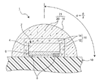
図1は、本発明の実施の形態1に係る発光装置1を示す模式断面図である。実装基板10の上に、半導体発光素子2がはんだバンプ8を介して固定され、その周囲を略均一な厚みで形成された蛍光体層16が覆っている。半導体発光素子2は、平面視で矩形の基板4上に青色光を発光可能な発光層を有する半導体層6を形成したものであり、半導体層6を下側、基板4を上側にしてフリップチップ実装されている。蛍光体層16は、透光性の蛍光体保持樹脂12に蛍光体粒子14を分散したものであり、蛍光体粒子14によって半導体発光素子2の発光する青色光(=1次光)の一部を吸収して黄色光などの長波長の光(=2次光)を発する。蛍光体層16の光出射側には、半導体発光素子2と蛍光体層16の全体を覆うように散乱層21が形成されている。図2は、半導体発光素子2の構造を示す模式断面図であり、サファイア等の透光性で絶縁性の基板4に、n側半導体層22、発光層24、p側半導体層26が順次積層されている。p側半導体層26と活性層24が一部除去されてn側半導体層22が露出しており、その露出面にn側電極32が形成されている。また、p側半導体層26には、反射性の電極28がほぼ全面に形成され、さらに外部と接続するためのp側電極30が形成されている。
FIG. 1 is a schematic cross-sectional view showing a
このような発光装置1では、半導体発光素子2の発する1次光と蛍光体層16の発する長波長の2次光との混色により、所望の色度の発光を得ることができる。例えば、蛍光体層16が黄色光を発する場合には、半導体発光素子2の発する青色光との混色によって、白色光が得られる。また、本実施の形態の発光装置1は、実装基板10の上に実装された半導体発光素子2の上面と四方の側面を遮光せずに透光性の材料で覆っているため、半導体発光素子2の上面と四方の側面に対向する発光装置の表面が全て光取り出し面となって効率良く光を取り出すことができる。特に、本実施の形態では、半導体発光素子2を半球ドーム状の散乱層21で覆っている。このため、半導体発光素子2を点光源として見ると、いずれの方位においても散乱層21の表面に対して垂直に光が出射することになり、散乱層21の表面での反射ロスが低減され、光取り出し効率が向上する。しかし、半導体発光素子2の示す発光強度分布と蛍光体層16の示す発光強度分布が異なる場合、発光装置1内の場所や、発光装置1を観察する方向によって色度が変化する色ムラが発生してしまう。特に、図1のように、半導体発光素子2の光軸を中心として180度の範囲において光を取り出す場合、半導体発光素子2の上方だけでなく、側方からも発光が観測されるため、半導体発光素子2と蛍光体層2の配光特性の違いによる色ムラが顕著となる。
In such a
図1に示すように、蛍光体層16は、半導体発光素子2の上面と四方の側面を略均一な厚みで覆うように形成されており、蛍光体層16内の蛍光体粒子14から全方位に長波長の2次光が発せられる。したがって、蛍光体層16から上方向に発する2次光と横方向に発する2次光の強度差は比較的小さい。また、蛍光体層16は、面内の場所による構造の変化がないため、どの場所でも一様に存在する。したがって、比較的均一な発光強度分布となる。これに対して、半導体発光素子2は、半導体層6に含まれる薄い発光層24から面状に1次光を発する。このため1次光の配光特性は、上方向と横方向が強く、斜め方向が弱いという特有の分布を持つ。また、半導体発光素子2は、図2に示すように複雑な電極構造を有しているため、発光層24に電流密度分布が生じ易く、電極30、32による光の遮蔽や吸収の影響も受ける。したがって、半導体発光素子2の発する1次光は、発光強度の面内分布も大きい。このため蛍光体層16の発光強度分布と半導体発光素子2の発光強度分布に違いがあり、色ムラが生じる。
As shown in FIG. 1, the
尚、本実施の形態のように、半導体発光素子2の周囲を略均一な厚みの蛍光体層16で薄く覆うことにより、蛍光体層16からの戻り光を減らし、高効率の発光が可能となる。しかし、その結果、蛍光体層16の発光強度分布と半導体発光素子2の発光強度分布の違いが大きくなり易く、色ムラが強くなる問題がある。即ち、半導体発光素子2の周囲を略均一な厚みの蛍光体層16で覆った場合、蛍光体層16は、半導体発光素子2の光出射側の主面に略平行な平面状の1つの光出射面と、半導体発光素子2の側面に略平行な平面状の4つの光出射面とを有することになる。前述の通り、蛍光体層16は層内の構造が均一であるため、蛍光体層16の発する2次光の強度は蛍光体層16を通過する1次光の光路長に依存する。本実施の形態のように、蛍光体層16が半導体発光素子2の光出射側の主面とほぼ平行な平面状の光出射面と半導体発光素子2の側面にほぼ平行な平面状の光出射面とを有する場合、半導体発光素子2のそれぞれの面に対して垂直な方向に出射する1次光が蛍光体層16を通過する光路長は蛍光体層16の厚みに一致するが、半導体発光素子2のそれぞれの面に対して斜めの方向に出射する1次光が蛍光体層16を通過する光路長は蛍光体層16の厚みよりも大きくなる。したがって、蛍光体層16から発する2次光の発光強度分布は、半導体発光素子2の面に対して垂直な方向に比べて、半導体発光素子2の面に対して斜め方向の方が発光強度が大きくなる。ところが、半導体発光素子2から出射する1次光の発光強度分布は、一般に全く逆の傾向を示し、半導体発光素子2のそれぞれの面に対して垂直な方向に比べて、半導体発光素子2のそれぞれの面に対して斜め方向の方が発光強度が小さくなる。このため蛍光体層16の発光強度分布と半導体発光素子2の発光強度分布に違いが一層顕著になり、強い色ムラが生じ易い。
Note that, as in the present embodiment, the periphery of the semiconductor
そこで本実施の形態の発光装置1では、半導体発光素子2の周囲に形成された散乱層21によって半導体発光素子2の発する1次光を選択的に散乱してから出射することを特徴とする。半導体発光素子2の1次光を選択的に散乱することにより、半導体発光素子の発光強度分布をより均一にできる。したがって、半導体発光素子2と蛍光体層16の発光強度分布の違いを小さくして、色ムラを抑制することができる。また、蛍光体層16の2次光を散乱層21によって強く散乱させないため、2次光の余計な散乱による半導体発光素子2や蛍光体層16への戻り光を減らし、光取り出し効率の低下も抑制することができる。したがって、色ムラと光取り出し効率を同時に改善し、明るく、色ムラの少ない発光装置を実現することができる。
Therefore, the
尚、この色ムラ改善の効果は、本実施の形態のように、半導体発光素子2を中心とする発光装置1の光出射角が大きい場合に特に顕著となる。発光装置1の光出射角θは、半導体発光素子を中心として発光装置から出射する光の角度範囲を指し、発光装置1の光軸方向から角度αの範囲に光線が出射している場合はθ=2αとなる。本実施の形態の場合は180°である。前述の通り、半導体発光素子2の発光層38は、薄い層状であるため、半導体発光素子2から出射する光の配光特性は、上方向と横方向が強く、斜め方向が弱いという特有の分布を持つ。したがって、発光装置の光出射角が大きい場合、半導体発光素子2の配光特性による色ムラが出易くなる。一方で、色ムラが抑制できるのであれば、発光装置の光出射角が大きい方が光源としては有利な場合が多い。本実施の形態では、散乱層21によって半導体発光素子2の配光特性の分布を改善できるため、発光装置1の光出射角を大きくしても色ムラを抑制できる。本件発明において、半導体発光素子2を中心とする発光装置1の光出射角は120°以上、より好ましくは150°以上、最も好ましくは180°以上とすることが望ましい。
The effect of improving the color unevenness is particularly remarkable when the light emission angle of the
散乱層21は、透光性の樹脂やガラスから成る透光性媒質18に粒子20を分散したものであり、粒子20の平均粒径Dを以下の範囲とすることにより、半導体発光素子2の発する1次光だけを選択的に散乱させることができる。以下の式において、λは半導体発光素子2の発する1次光が透光性媒質18中で示す波長である。
20nm<D≦0.4×λ/π [式1]
The
20 nm <D ≦ 0.4 × λ / π [Formula 1]
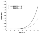
粒子20による散乱理論は、サイズパラメータα=πD/λによって変わり、α≦0.4ではレイリー散乱、0.4<α<3ではミー散乱、それ以上では回折散乱となる。したがって、粒子20の粒径Dが(0.4×λ/π)以下であることにより、半導体発光素子2の1次光に対してレイリー散乱が起きる。例えば、透光性媒質18の屈折率が1.4〜1.5である場合、空気中での波長が450nmの青色光に対しては、粒径Dが約40nm以下であればレイリー散乱領域となる。
The scattering theory by the
レイリー散乱領域では、散乱係数ksは以下の式で示される。

図3は、粒子20の数nが8,500,000,000、粒子20の屈折率が2.15、透光性媒質18の屈折率が1.41である場合の粒子の粒径Dと散乱係数ksの関係を、波長450nmの光と波長550nmの光について示したグラフである。図2に示される通り、粒子の粒径Dが40nm以下のレイリー散乱領域にある場合、450nmの光は550nmの光に比べて2倍以上強く散乱される。しかし、散乱係数ksは、粒径Dが小さくなるに従って低下していき、粒子20の粒径Dが20nm以下になるといずれの波長の光に対する散乱強度も低下してしまう。そこで本件発明では、粒子20の平均粒径Dを20nmよりも大きく設定する。粒子の平均粒径が20nm以上であれば、粒子の数を適宜制御することによって可視域である1次光に対して必要な散乱強度を得ることができる。粒子の平均粒径が20nm以下であると、粒子の数を相当高めなければ必要な散乱強度が得られないが、粒子の数を高くしすぎると樹脂中への分散が困難になる。したがって、粒子20の粒径Dを20nmよりも大きく、かつ、(0.4×λ/π)nm以下とすれば、半導体発光素子2の1次光を蛍光体層16の発する長波長の2次光に対して選択的に散乱することができる。
FIG. 3 shows the particle diameter D when the number n of the
また、図1に示す発光装置では、散乱層21内の粒子20として屈折率が透光性媒質18よりも高い無機材料を用いている。例えば、透光性媒質18として屈折率が1.41〜1.53のシリコーン樹脂やエポキシ樹脂を用い、粒子として屈折率が2.15であるジルコニアを用いることができる。これによって、散乱層21の実効屈折率を高めて、発光装置1の光取り出し効率を向上することができる。即ち、図1に示す発光装置では、半導体発光素子2が、基板4を上側にしてフリップチップ実装されているため、基板4から発した光は、基板4と蛍光体層16の界面と、蛍光体層16と散乱層21の界面とを通じて外部に取り出される。屈折率の大きな媒質から屈折率の小さな媒質に入射する光は、その屈折率差に応じて決まる臨界角よりも大きな入射角で入射した光は界面で全反射してしまう。したがって、半導体発光素子2で生じた1次光を効率よく発光装置1の外部に取り出すためには、散乱層21と蛍光体層16の屈折率が、基板4の屈折率にできるだけ近いことが好ましい。半導体発光素子2の基板4に用いられる材料の屈折率は、一般に1.7から2.5程度である(例えば、サファイアでは約1.76)。透光性媒質18に高屈折率の粒子20を分散させることにより、散乱層21の屈折率を透光性媒質18の持つ1.41〜1.53から基板4に近い値にまで高めることが可能となる。散乱層21と基板4の実効屈折率差は、0.2以下、より好ましくは0.05以下であることが望ましい。基板4と散乱層21の屈折率が近ければ、間に介在する蛍光体層16の屈折率を両者に近い値に設定することにより、各界面での実効屈折率差を小さくして、反射ロスを低減することができる。したがって、発光装置1からの光取り出し効率が向上する。基板4を下側にしてフェースアップ実装する場合も、同様の屈折率であることが望ましい。また、例えば半導体発光素子の基板を除去して半導体層のみとする場合は、半導体発光素子を構成する半導体と散乱層の実効屈折率差が、0.2以下、より好ましくは0.05以下であることが望ましい。半導体発光素子の側面から出射する光を利用するためには、図1に示す発光装置にように、透光性の基板を有する半導体発光素子を用いることが望ましい。
Further, in the light emitting device shown in FIG. 1, an inorganic material having a higher refractive index than that of the
以下、本実施の形態において発光装置10を構成する各部材について詳細に説明する。
Hereinafter, each member which comprises the light-emitting
(散乱層21)
散乱層21は、透光性媒質18に粒子20を分散して構成されている。本実施の形態のように発光装置の出射角が大きい場合、半導体発光素子2と蛍光体層16の周囲を広い角度範囲に渡って散乱層21で覆うことが好ましい。散乱層21は、半導体発光素子2から出射した1次光が散乱を受けない場合の光線軌跡を考えて、発光装置1の出射角の範囲内にある光線が通過する領域に配置される。好ましくは、このような領域は全て散乱層21で覆う。本実施の形態では、散乱層21は、半導体発光素子2と蛍光体層16の全体を覆うように半球状に形成されている。散乱層21が半球状であれば、散乱層21と外部(空気)との界面における反射ロスが減るため好ましい。散乱層21は、半導体発光素子2の1次光を散乱させることができれば、どこに配置されていても良い。但し、半導体発光素子2の発光強度分布を改善するため、平面視において、矩形の半導体発光素子2が散乱層21の中心に位置することが好ましい。また、断面視において、散乱層21が半導体発光素子2の上面と側面を覆うようにすることが好ましい。散乱層21は、蛍光体層16の光出射側に配置する。尚、蛍光体層16の光出射側とは、蛍光体層16の2つの主面のうち半導体発光素子の1次光を受ける面とは逆の主面がある側を指す。蛍光体層16の光出射側に散乱層21を配置することにより、蛍光体層16を通過後の1次光の発光強度分布を改善できるため、最終的に色ムラを抑制し易い。一方で、散乱層21は蛍光体層16の2次光を強く散乱することはないので、2次光の余計な散乱による戻り光の増加も抑制できる。蛍光体層16の光出射側にある主面の全面を散乱層21で覆うことが好ましい。
(Scattering layer 21)
The
(a)粒子20
粒子20は、それを分散させる透光性媒質18と異なる屈折率を持つ材料であれば光散乱の機能を発揮できるが、透光性媒質18よりも高い屈折率を持つことが好ましい。これにより、発光装置1の光取り出し効率をさらに高め、信頼性も向上することができる。即ち、粒子20が高い屈折率を持つことにより、散乱層21の実効屈折率を高めて光取り出し効率を向上することができる。また、透光性媒質18の材料選択の幅が広がるため、透光性媒質18として耐久性の高い材料を用いることも可能となる。
(A)
The
また、粒子20として無機材料、有機材料、複合材料等の種々の材料を用いることができるが、粒子20が無機材料であれば、粒子20自身の耐久性、熱伝導率、屈折率が高くなるため好ましい。粒子20の熱伝導率が高くなれば、散乱層21を通じた放熱効率も向上する。
In addition, various materials such as an inorganic material, an organic material, and a composite material can be used as the
そのような粒子20としては屈折率の高い無機材料(特に、酸化物、窒化物、硫化物)を用いることが好ましい。例えば、酸化チタン、酸化ニオブ、酸化アルミニウム、酸化イットリウム、酸化ジルコニウム、ダイヤモンド、酸化タンタル、酸化セリウム、イットリウム・アルミニウム・ガーネット(YAG)、イットリウム・バナデート(YVO4)、酸化インジウム、硫化亜鉛、窒化珪素等を挙げることができる。中でも酸化ジルコニウム、酸化ニオブを用いることが望ましい。粒子20は、蛍光体とは異なる材料を用いることが望ましい。
As
粒子20の屈折率は、1.7以上、より好ましくは2.0以上であることが望ましい。粒子20の屈折率が透光性媒質18の屈折率に比べて高いほど、粒子20による1次光の散乱が強くなり、また、散乱層21の実効屈折率が高くなるからである。一方、粒子20の屈折率は、通常得られる範囲であれば高すぎることはない。粒子20の屈折率が高くなれば、透光性媒質18との屈折率差が大きくなって散乱強度も高まるが、散乱強度が強すぎる場合には、粒子20の数によって散乱強度を適当な範囲に制御できるからである。このような屈折率は、特に、半導体発光素子の発光する1次光のピーク波長が420〜500nmである場合に望ましい。
The refractive index of the
粒子20の平均粒径Dは、上記(式1)を充足することが必要であるが、半導体発光素子の1次光に対する散乱強度を高めるために、上記(式1)の範囲内で平均粒径Dが大きなことが好ましい。平均粒径Dは、好ましくは25nm以上、さらに好ましくは30nm以上とすることが望ましい。尚、粒子20が球状でない場合は、粒子20の最大径で粒径を考える。
The average particle diameter D of the
透光性媒質18中における粒子20の分散量(重量%)は、10%以上、より好ましくは50%以上であることが望ましい。粒子20による散乱強度は、上記(式2)に示されるように粒子20の数にも依存するためである。また、粒子20の分散量が多いほど、散乱層21の熱伝導率も向上する。一方、粒子20の分散量が多すぎると、散乱層21から半導体発光素子2や蛍光体層16への戻り光が増加して、光取り出し効率が低下する。そこで粒子20の分散量は、80%以下、より好ましくは70%以下であることが望ましい。
The dispersion amount (% by weight) of the
尚、本件発明の散乱層21は、半導体発光素子2の1次光を散乱してから外部に出射させることが目的であるため、半導体発光素子2の1次光の戻り光が増えて、半導体発光素子2の利用率が低下しないようにすることが重要である。そのため、半導体発光素子2から出射する1次光のうち、80%以上、より好ましくは90%以上が発光装置1の外部に出射できるように、散乱層21における粒子20の数、粒径、屈折率等を制御することが望ましい。
Since the
散乱層21における粒子20の分布は、特に限定されない。但し、半導体発光素子2の側から光取り出し側(空気側)に向かって密度が低くなるような分布にすれば、半導体発光素子2の側(屈折率1.76)では実効屈折率を高くし、外部の空気に接する側(屈折率1)では実効屈折率が低くなるため、有利である。
The distribution of the
(b)透光性媒質18
透光性樹脂18には、無色で透過率が高く、均質で、高い等方性、耐久性を持つことが望ましいが、このような光学特性を満たす材料は限られており、その屈折率はn=1.4から1.54程度の範囲となってしまう。これは、短波長の可視光を発光する半導体発光素子に一般的に用いられるサファイアやIII−V族半導体といった材料に比べて低くなる。このため半導体発光素子から透光性樹脂を経て発光装置の外部に至る光路において、屈折率差の大きな界面が存在することになり、その界面での全反射により光取り出しが制限されてしまう。このことによっても、発光装置の光取り出し効率は低下する。本実施の形態では、透光性媒質18中に高屈折率の粒子20を分散しているため、透光性媒質18の屈折率を高めて光取り出し効率を高めることができる。
(B)
The
透光性媒質18としては、半導体発光素子2の光に対して透光性を持つ有機材料や無機材料を用いることができる。有機材料としては、透光性を持つ樹脂を用いることができる。例えば、シリコーン樹脂組成物、変性シリコーン樹脂組成物等を使用することが好ましい。エポキシ樹脂組成物、変性エポキシ樹脂組成物、アクリル樹脂組成物等の透光性を有する絶縁樹脂組成物を用いることもできる。また、これらの樹脂を少なくとも一種以上含むハイブリッド樹脂等、耐候性に優れた樹脂も利用できる。また、無機材料としては、ガラス等のアモルファス材料、無機結晶、セラミックなどを用いることができる。透光性媒質18として、シリコーン樹脂組成物、変性シリコーン樹脂組成物等を使用することが好ましい。エポキシ樹脂組成物、変性エポキシ樹脂組成物、アクリル樹脂組成物等の透光性を有する絶縁樹脂組成物を用いれば、硬化後も無色透明であり、均質で、高い等方性を有するという優れた光学材料特性を有し、しかも安価で成型も容易であるため好ましい。これらの材料は、屈折率が1.4〜1.54程度と低いが、屈折率の高い粒子を分散することで実効屈折率を高めることができる。
As the
透光性媒質18として、特に、フェニル基を導入しないシリコーン樹脂組成物やフェニル基を有しない変性シリコーン樹脂組成物、例えば、メチル系のシリコーン樹脂組成物やメチル系の変性シリコーン樹脂組成物を用いれば、発光装置の信頼性を高めることができる。フェニル基を導入すると、透光性媒質18の屈折率が高くなる一方で、透光性媒質18の耐光性と耐熱性が低下するためである。高屈折率の粒子20を分散することにより、透光性媒質18にフェニル基を導入しなくても散乱層21の実効屈折率を高くできる。
As the
一方、透光性媒質18として、フェニル基を導入したシリコーン樹脂組成物や変性シリコーン樹脂組成物を用いれば、透光性媒質18の屈折率を高くすることができる。そこに高屈折率の粒子20を分散することで、散乱層21の実効屈折率を一層高め、発光装置1の光取り出し効率を向上することができる。
On the other hand, if a silicone resin composition into which a phenyl group is introduced or a modified silicone resin composition is used as the
尚、散乱層21の実効屈折率は、Maxwell−Garnet理論に基づいて、透光性媒質18の比誘電率と粒子20の比誘電率から見積もることができる。また、透光性媒質18及び粒子20は、半導体発光素子2の1次光に対して透光性であることが重要であるが、半導体発光素子2の1次光は可視光であるため、可視域の外側にある紫外光に対して吸収を持つ材料であっても構わない。
The effective refractive index of the
(蛍光体層16) (Phosphor layer 16)
本実施の形態のように発光装置の出射角が大きい場合、半導体発光素子2の周囲を広い角度範囲に渡って蛍光体層16で覆うことが好ましい。半導体発光素子2から出射した1次光が散乱を受けない場合の光線軌跡を考えて、発光装置1の出射角の範囲内にある光線が通過する領域は全て蛍光体層16で覆うことが好ましい。蛍光体層16は、種々の形態とすることができる。例えば、透光性の樹脂から成る蛍光体保持部材中に無機材料から成る蛍光体粒子を含有させて蛍光体層としても良い。蛍光体層16は、半導体発光素子2の周りに、ポッティング、スクリーン印刷等の種々の手法により形成することができる。蛍光体層16は、半導体発光素子2の発光の一部を吸収して長波長の光を発光可能なものであれば特に限定されない。蛍光体層16は、本実施の形態のように、蛍光体粒子14をガラスや樹脂などの蛍光体保持部材12に含有させた部材でも良いし、蛍光体の結晶やアモルファス体から成るものでも良い。
When the emission angle of the light emitting device is large as in the present embodiment, it is preferable to cover the periphery of the semiconductor
蛍光体粒子14としては、青色光で励起されて黄色のブロードな発光を示す蛍光体を用いれば、演色性の良い白色が得られるため好ましい。特に、無機材料から成る蛍光体粒子14を用いれば、半導体発光素子2からの強い熱や光にも耐久性があるため好ましい。蛍光体の発光ピーク波長は、500〜600nm、より好ましくは520〜560nmにあることが好ましい。このような蛍光体粒子14として、例えば、セリウムで付活されたガーネット構造を持つ蛍光体(特に、セリウムで付活され、アルミニウムを含みガーネット構造を持つ蛍光体)が挙げられる。セリウムで付活された蛍光体は、黄色にブロードは発光を示すため、青色発光との組合せによって演色性の良い白色を実現できる。また、ガーネット構造、特にアルミニウムを含むガーネット構造の蛍光体は、熱、光、水分に強く、高輝度な黄色発光を長時間維持することができる。例えば、波長変換物質として、(Re1-xSmx)3(Al1-yGay)5O12:Ce(0≦x<1、0≦y≦1、但し、Reは、Y、Gd、La、Lu、Tbからなる群より選択される少なくとも一種の元素である。)で表されるYAG系蛍光体(一般にYAGと略記される)を用いることが好ましい。また、黄色蛍光体の他に、Lu3Al5O12:Ce、BaMgAl10O17:Eu、BaMgAl10O17:Eu,Mn、(Zn,Cd)Zn:Cu、(Sr,Ca)10(PO4)6Cl2:Eu,Mn、(Sr,Ca)2Si5N8:Eu、CaAlSiBxN3+x:Eu及びCaAlSiN3:Euなどの蛍光体を用いて演色性を調整することもできる。
As the
一方、蛍光体粒子14を含有する蛍光体保持部材12としては、半導体発光素子2の光に対して透光性を持つ有機材料や無機材料を用いることができる。有機材料としては、透光性を持つ樹脂が好ましい。例えば、シリコーン樹脂組成物、変性シリコーン樹脂組成物等を使用することが好ましいが、エポキシ樹脂組成物、変性エポキシ樹脂組成物、アクリル樹脂組成物等の透光性を有する絶縁樹脂組成物を用いることができる。また、これらの樹脂を少なくとも一種以上含むハイブリッド樹脂等、耐候性に優れた樹脂も利用できる。また、無機材料としては、ガラス等のアモルファス材料、無機結晶、セラミックなどを用いることができる。尚、前述の通り、蛍光体の結晶やアモルファス体自身を蛍光体層16とした場合には、蛍光体保持部材12は不要となる。
On the other hand, as the
(半導体発光素子2)
半導体発光素子2は、半導体から成る発光層を備えたものであれば良い。特に窒化物半導体から成る発光層、中でも窒化ガリウム系化合物半導体(特にInGaN)から成る発光層を備えた発光素子であれば、青色域で強い発光が可能であるため、蛍光体層16と好適に組み合わせることができる。半導体発光素子2は、発光層24から出力される光のピーク波長が、可視域であれば良いが、420nm〜500nm、より好ましくは、445〜465nmにあることが望ましい。この波長域で青色光を発光する半導体発光素子2であれば、種々の蛍光体層16との組合せにより、所望の色、特に白色光の発光が可能となる。尚、半導体発光素子2は、ZnSe系、InGaAs系、AlInGaP系などの半導体から成る発光層を有するものでも良い。また、半導体発光素子2は、基板4の下面又は、半導体層6の上面から光を取り出す面発光タイプの発光ダイオードであることが好ましい。
(Semiconductor light emitting element 2)
The semiconductor
図1に示すように、本実施の形態では、発光素子2の基板4を上側にして実装基板10の上にフリップチップ実装している。実装基板10の上面には電極が形成されており(図示せず)、はんだバンプ8を介して、半導体発光素子2のp側30及びn側電極32と接続される。
As shown in FIG. 1, in this embodiment, the
尚、本発明で用いることのできる半導体発光素子2は、図2に示す構造のものに限定されない。例えば、各導電型層に、絶縁、半絶縁性、逆導電型構造が一部に設けられても良い。また、基板4は、導電性を持つものでも良く、その場合には、n側電極32を基板4の裏面に形成しても良い。また、基板4は、半導体層6を成長させる際の基板であっても良いし、半導体層6を成長させた後で貼りあわせたものでも良い。基板4は、除去することもできる。例えば、基板4を含む半導体発光素子2をフリップチップ実装し、その後で基板4を剥離しても良い。
The semiconductor
(実装基板10)
実装基板10は、表面に半導体発光素子2と電気的に接続される配線を形成したものであれば良い。本実施の形態では、平板状の絶縁部材に配線を形成して実装基板10としている。絶縁部材として、窒化アルミニウムやアルミナ等のセラミック、ガラスを用いることができる。また、Si等の半金属あるいは金属の表面に窒化アルミニウム等の絶縁性の薄膜層を形成して用いても良い。これらの実装基板10は、放熱性が高いため、好ましい。また、配線は、イオンミリング法或いはエッチング法等によって金属層のパターニングを施すことによって形成できる。例えば、窒化アルミニウムの表面に白金薄膜等からなる配線パターンを形成できる。更に、配線パターンを保護する目的で、SiO2等の薄膜からなる保護膜を形成してもよい。
(Mounting board 10)
The mounting
実施の形態2.
図4は、本件発明の実施の形態2に係る発光装置を示す断面図である。図4の発光装置1は、内側から順番に、赤色を発光する第1蛍光体層16aと黄色を発光する第2蛍光体層16bの2層を有する。これによって、黄色を発光する蛍光体層16だけが形成された場合に比べて、赤味成分を増し、平均演色評価数Raの高い発光装置とすることをもできる。平均演色評価数Raの高い発光装置とすれば照明用途に適した発光装置となる。また、赤味成分を増やすことで、電球色を発光する発光装置とすることもできる。その他の点は、実施の形態1と同様である。
FIG. 4 is a cross-sectional view showing a light emitting device according to
第1蛍光体層16aには、黄〜赤色発光を有する蛍光体粒子14aを含むことが好ましい。可視光を黄色〜赤色域に変換する蛍光体としては、窒化物蛍光体、酸窒化物蛍光体、珪酸塩蛍光体などが挙げられる。
The
窒化物系蛍光体、酸窒化物(オキシナイトライド)蛍光体としては、Sr−Ca−Si−N:Eu、Ca−Si−N:Eu、Sr−Si−N:Eu、Sr−Ca−Si−O−N:Eu、Ca−Si−O−N:Eu、Sr−Si−O−N:Euなどが挙げられる。窒化物蛍光体及び酸窒化物蛍光体の中でも、アルカリ土類窒化ケイ素蛍光体が好ましく、次の一般式で表すことができる(Lは、Sr、Ca、SrとCaのいずれか)。
LSi2O2N2:Eu、LxSiyN(2/3x+4/3y):Eu、LxSiyOzN(2/3x+4/3y-2/3z):Eu
Nitride-based phosphors and oxynitride (oxynitride) phosphors include Sr—Ca—Si—N: Eu, Ca—Si—N: Eu, Sr—Si—N: Eu, and Sr—Ca—Si. -O-N: Eu, Ca-Si-O-N: Eu, Sr-Si-O-N: Eu, etc. are mentioned. Among the nitride phosphors and oxynitride phosphors, alkaline earth silicon nitride phosphors are preferable, and can be represented by the following general formula (L is any one of Sr, Ca, Sr and Ca).
LSi 2 O 2 N 2: Eu , L x Si y N (2 / 3x + 4 / 3y): Eu, L x Si y O z N (2 / 3x + 4 / 3y-2 / 3z): Eu
珪酸塩蛍光体としては、L2SiO4:Eu(Lはアルカリ土類金属)、
(SrxMae1-x)2SiO4:Eu(MaeはCa、Baなどのアルカリ土類金属)などが好ましい。
As the silicate phosphor, L 2 SiO 4 : Eu (L is an alkaline earth metal),
(Sr x Mae 1-x ) 2 SiO 4 : Eu (Mae is an alkaline earth metal such as Ca or Ba) is preferred.
一方、第2蛍光体層16bには、青色光で励起されて励起されて黄色のブロードな発光を示す蛍光体粒子14bを用いる。このような蛍光体粒子14bとして、実施の形態1で説明したのと同様の材料を用いることができる。
On the other hand, for the
尚、本実施の形態では、赤色発光する第1蛍光体層16aと黄色発光する第2蛍光体層16bを有する場合について説明したが、本件発明はこれに限定されない。互いに発光波長が異なる2種類の蛍光体であれば何を用いても良い。発光波長の異なる2種類の蛍光体を用いることで、発光装置の発する光の演色性が向上する。また、本実施の形態では、2種類の蛍光体粒子14a、14bを、別々の蛍光体層16a、16bに分けて保持する例について説明したが、単一の蛍光体層16内に2種類の蛍光体粒子を含んでいても良い。また、半導体発光素子2からの1次光によって1種類目の蛍光体を励起、発光させ、その蛍光体の発する2次光によって別の種類の蛍光体を励起、発光させることもできる。また、色度の異なる2種類の蛍光体を用いれば、2種類の蛍光体の量を調整することにより、色度図上において2種類の蛍光体と発光素子の色度点を結んでできる領域内の任意の色度点に対応する発光を得ることができる。
In the present embodiment, the case where the
実施の形態3.
図5は、本件発明の実施の形態3に係る発光装置を示す断面図である。図5の発光装置1は、蛍光体層16にも高屈折率の無機材料から成る粒子20が分散している。この点を除けば、実施の形態1と同様である。
Embodiment 3 FIG.
FIG. 5 is a cross-sectional view showing a light-emitting device according to Embodiment 3 of the present invention. In the
蛍光体層16に、蛍光体保持部材12よりも高い屈折率を持つ成る粒子20を散乱すれば、蛍光体層16の屈折率を高めることができる。したがって、基板4と蛍光体層16との界面、蛍光体層16と散乱層21との界面において全反射が起きる臨界角を大きくし、界面での反射ロスを低減することができる。また、蛍光体層16にも無機材料から成る粒子20を分散することにより、蛍光体層16の熱伝導率を高めることができ、発光装置1の信頼性も向上する。さらに、蛍光体層16にも粒子20が分散していれば、半導体発光素子2の1次光の発光強度分布も改善される上、蛍光体層16中の蛍光体粒子14に入射する1次光の割合も増加する。一方、蛍光体層16に分散する粒子20は、平均粒径Dが上記(式1)を充足しており、蛍光体粒子14の発する長波長の2次光を強く散乱しないため、余計な戻り光の増加による光取り出し効率の低下も抑制できる。
If the
本実施の形態において蛍光体層16に粒子20を分散するには、蛍光体層16をポッティング、印刷などで形成する際に、蛍光体粒子14と共に粒子20を分散しておけば良い。尚、蛍光体層16を電気泳動により形成する場合、蛍光体層16を形成した後に、粒子20を含む樹脂にて含浸しても良い。例えば、蛍光体層16の形成後に、粒子20を分散した透光性媒質18の硬化前溶液に含浸すれば良い。また、蛍光体層16に分散する粒子20は、上記(式1)を充足するものであれば良く、散乱層21に分散する粒子20と同一であっても良いし、異なる材料であっても良い。但し、散乱層21に分散する粒子20と同一にすれば、発光装置1の製造工程が簡易になるため有利である。尚、蛍光体層16に分散させる粒子20の濃度は、散乱層21に分散させる粒子20の濃度よりも高いことが好ましい。屈折率の高い粒子20を多く含有させることにより、屈折率を高めることができる。このため、蛍光体層16の屈折率よりも、発光装置1の光取り出し側に配置された散乱層21の屈折率を低くすることで、発光装置の屈折率が、半導体発光素子2から光取り出し側に向かって、装置の外側にある空気の屈折率に段階的に近づいていくため、1次光及び2次光を効率よく発光装置1の外部に取り出すことができる。
In order to disperse the
実施の形態4.
図6は、実施の形態4に係る発光装置を示す模式断面図である。本実施の形態では、半導体発光素子2が半導体層6を上面にしてフェースアップ実装され、半導体発光素子2を実装基板10に接着するダイボンド剤38に粒子20が分散されている。その他の点は、実施の形態3と同様である。
FIG. 6 is a schematic cross-sectional view showing the light emitting device according to the fourth embodiment. In the present embodiment, the semiconductor
図6に示すように、半導体発光素子2の基板4は実装基板10の表面にダイボンド剤38によって固定されている。ダイボンド剤38は、半導体発光素子2の底面のほぼ全面に塗布されている。半導体発光素子2の半導体層6に形成されたp側電極及びn側電極(図示せず)は、ワイヤー36によって実装基板10上の電極(図示せず)に接続されている。半導体発光素子2を実装基板10に固定するダイボンド剤38には、ダイボンド剤38を構成する樹脂よりも高い屈折率を持った無機材料から成る粒子20が分散されている。ダイボンド剤38の周囲は、蛍光体層16と散乱層21によって覆われている。
As shown in FIG. 6, the
本実施の形態のように、半導体発光素子2を実装基板10に固定するダイボンド剤38に、ダイボンド剤38を構成する樹脂よりも屈折率の高い無機材料から成る粒子20を分散することにより、ダイボンド剤38の屈折率が半導体発光素子2の基板4の屈折率に近くなる。このため基板4とダイボンド剤38との界面における反射光が減り、半導体発光素子2内への戻り光が減少して、光取り出し効率が向上する。また、ダイボンド剤38内で半導体発光素子2の1次光が散乱することにより、実装基板10の表面にある金属電極に到達する光が減り、そこでの吸収ロスを低減できる。また、ダイボンド剤38の屈折率が基板4の屈折率に近づき、ダイボンド剤38内で粒子20によって1次光が散乱する結果、基板4の裏面に光の多重反射防止用の凹凸をつけたのと同様の効果が得られる。したがって、半導体発光素子2内における光の多重反射による吸収ロスを減少し、発光装置1の光取り出し効率が向上できる。また、ダイボンド剤38に無機材料から成る粒子20が分散することにより、ダイボンド剤38の熱伝導率も向上するため、発光装置1の放熱効率が改善し、信頼性が向上する。尚、ダイボンド剤38は、膜厚を例えば2μm以下にでき、散乱層21や蛍光体層16に比べて極めて薄くできる。したがって、散乱層21や蛍光体層16に比べて、ダイボンド剤38に分散させる粒子20の密度を高くすることができる。
As in the present embodiment, the
本実施の形態のように、半導体発光素子2が半導体層6を上面にしてフェースアップ実装された場合も、上述の実施の形態と同様に、散乱層21と基板4の実効屈折率差は、0.2以下、より好ましくは0.05以下であることが望ましい。特に基板4が透光性である場合、基板4は半導体層6と屈折率の近いものを選択するためである。基板4と散乱層21の屈折率が近ければ、間に介在する蛍光体層16の屈折率を両者に近い値に設定することにより、各界面での実効屈折率差を小さくして、反射ロスを低減することができる。したがって、発光装置1からの光取り出し効率が向上する。また、半導体層6を基準として、半導体層6と散乱層21の実効屈折率差を、0.2以下、より好ましくは0.05以下とすることもできる。
As in the present embodiment, when the semiconductor
尚、ダイボンド剤38に分散する粒子20は、上記(式1)を充足するものであれば良く、散乱層21や蛍光体層16に分散する粒子20と同一材料でも良いし、異なる材料としても良い。また、本実施の形態では、半導体発光素子2をフェースアップ実装する場合について説明したが、フェースダウン実装する場合には、半導体発光素子と実装基板との間に充填される樹脂部材に本実施の形態の構成を適用しても良い。
The
実施の形態5.
図7は、本発明の実施の形態5に係る発光装置を模式的に示す断面図である。本実施の形態では、半導体発光素子2が基板4を上側にしてフリップチップ実装され、基板4の上面に板状の蛍光体層16aが接着層40を介して接着されている。また、半導体発光素子2の四方の側面にも、同じ接着層40を介して板状の蛍光体層16bが形成されている。板状の蛍光体層16a及び16bは、下面が開口した箱型の形状となっている。その他の点は、実施の形態1と同様である。例えば、本実施の形態においても、実施の形態1と同様に、蛍光体層16は、半導体発光素子2の光取り出し側の主面とほぼ平行な平面状の1つの光出射面と、半導体発光素子2の側面にほぼ平行な平面状の4つの光出射面とを有することになる。
FIG. 7 is a cross-sectional view schematically showing a light emitting device according to
本実際の形態では、板状の蛍光体層16a、16bと半導体発光素子2を接着する接着層40に、その接着層40の材料よりも高い屈折率を持った無機材料から成る粒子20が分散されている。これによって接着層40の実効屈折率が増加するため、半導体発光素子2と接着層40との界面、及び接着層40と蛍光体層16a、16bとの界面における実効屈折率差を小さくし、全反射の臨界角を高くして、反射による戻り光を低減できる。また、蛍光体層16a、16bには、接着層40で散乱された後の青色光が入射することになるため、蛍光体層16a、16bの励起がより均一に行われ、蛍光体層16a、16bの発光強度分布が改善される。また、半導体発光素子2の1次光も、接着層40と散乱層21で2回散乱されることになり、半導体発光素子2の発光強度分布もより均一になる。さらに、半導体発光素子2から、接着層40、蛍光体層16a、16bに至る経路の放熱効率も高まる。
In this actual embodiment,
本実施の形態で用いる板状の蛍光体層16a、16bは、無機材料から成ることが好ましい。特に、熱伝導率が0.8[W/mK]以上、より好ましくは1.0[W/mK]以上、さらに好ましくは4.0[W/mK]以上の無機材料で構成することが望ましい。具体的には、無機系蛍光体の結晶やアモルファス体自身を蛍光体層16a、16bとしたり、無機系の蛍光体粒子をガラスやアルミナ等の無機材料から成る透光性部材に含有させて蛍光体層16a、16bとすることができる。無機系蛍光体の結晶やアモルファス体自身を蛍光体層16a、16bとする場合の例としては、セリウムで付活されたガーネット構造を持つ蛍光体の結晶を板状体としたものが挙げられる。また、無機系の蛍光体粒子を無機材料から成る透光性部材に含有させる場合、無機材料の透光性部材としてはガラス等のアモルファス材料、無機結晶、セラミックなどを用いることができる。このような材料で蛍光体層16a、16bを構成することにより、蛍光体層16a、16b自身の耐久性が高まると同時に、蛍光体層16a、16bから実装基板10に向かう放熱も良好になり、信頼性の高い発光装置1を実現することができる。尚、蛍光体層16a、16bが、「板状」であるためには、全体の形状が板状であれば良く、表面に凹部や孔を有していても良い。また、何らかの光学効果を得るためのパターンが表面に形成されていても良い。蛍光体層16a、16bが「板状」である場合に、平面形状は矩形に限らず、円形、楕円形など種々の形状でも良い。板状の蛍光体層16は、半導体発光素子2の基板主面と平行に設置することが好ましい。蛍光体層16が板状であれば、半導体発光素子2に板状体を固着するだけで蛍光体層16が形成できる。また、蛍光体層16を板状にすれば、発光装置1を生産する際に蛍光体層16を大きめの板状材料として加工しておき、それを所望の大きさに切り出して使うことができるため、発光装置の組立が容易となる。
The plate-like phosphor layers 16a and 16b used in the present embodiment are preferably made of an inorganic material. In particular, it is desirable to use an inorganic material having a thermal conductivity of 0.8 [W / mK] or more, more preferably 1.0 [W / mK] or more, and even more preferably 4.0 [W / mK] or more. . Specifically, the
尚、半導体発光素子2の側面に形成する蛍光体層16bは、板状部材の接着ではなく、印刷等によって形成しても良い。また、接着層40に分散する粒子20は、上記(式1)を充足するものであれば良く、散乱層21に分散する粒子20と同一材料であっても、異なる材料であっても良い。
In addition, you may form the
実施の形態6.
図8は、本発明の実施の形態6に係る発光装置1を示す模式断面図である。本実施の形態では、半導体発光素子2の側面に形成されていた蛍光体層16bに代えて、蛍光体層16aの2次光を1次光と共に散乱しながら反射する反射部材45が形成されている。また、散乱層21は、半導体発光素子2の上方にある蛍光体層16aの上面のみを覆い、半導体発光素子2の側方には形成されていない。したがって、本実施の形態では、蛍光体層16は、半導体発光素子2の主面とほぼ平行な平面状の1つの光出射面から2次光が取り出される。この場合でも、実施の形態1で説明したのと同様の理由により、半導体発光素子2の主面に対して垂直な方向に比べて、斜め方向の方が2次光の発光強度が大きくなり、蛍光体層16の2次光が持つ発光強度分布は半導体発光素子2の持つ1次光の発光強度分布と逆の傾向となる。したがって、実施の形態1乃至5と同様の理由により、色ムラが生じやすい。その他の点は、実施の形態5と同様である。
FIG. 8 is a schematic cross-sectional view showing the
本実施の形態のように、蛍光体層16aが板状である場合、平面内の分布を考えると、板の端面における発光が強くなる傾向にある。そこで、本実施の形態のように、蛍光体層16aが板状であり、半導体発光素子の上面に固定されているような場合には、蛍光体層16aの上面に散乱層21を形成し、蛍光体層16aの側面に反射部材45を設け、その反射部材45によって蛍光体層16aの2次光を散乱しながら反射することが好ましい。また、図8に示すように、この反射部材45は半導体発光素子2の側面にも設けることが好ましい。
In the case where the
反射部材45においては、樹脂42中に比較的粒径の大きな散乱粒子44が分散されている。散乱粒子44の平均粒径は、半導体発光素子2の青色光に対して散乱機構がミー散乱又は回折散乱となる大きさに設定されており、半導体発光素子2の発する青色光と蛍光体層16aの発する長波長の光を両方散乱する。具体的には、散乱粒子44の平均粒径D’を70nm以上、より好ましくは200nm以上とする。散乱粒子44の平均粒径を70nm以上とすれば、透光性媒質42の屈折率が1.4以上であれば、可視域の光に対してミー散乱か回折散乱とすることができる。散乱層21は、半導体発光素子からの1次光を選択的に散乱するものであったが、反射部材45では、半導体発光素子2の1次光と蛍光体層16aの2次光の両方を散乱しながら反射させることができる。尚、反射部材45の散乱粒子44は、散乱層21の粒子20と同様の材料を用い、平均粒径を大きくしてミー散乱又は回折散乱領域としても良い。また、反射部材45の樹脂42も、散乱層21の透光性媒質18と同様の材料によって構成することができる。
In the reflecting
この反射部材45は、半導体発光素子2の側方に形成されている。そのため、反射部材45の散乱によって、半導体発光素子2の側面から出射する1次光と蛍光体層16aの側面や下面から出射する2次光とを散乱しながら反射することができ、色ムラの少ない発光が得られる。一方、半導体発光素子2の上面から出射した青色光は、蛍光体層16aを通過した後、半導体発光素子2の1次光を選択的に散乱する散乱層21を通過して出射される。本実施の形態によれば、実施の形態5よりも簡易な構成により、色ムラの少ない発光装置を得ることができる。尚、反射部材45は、半導体発光素子2の側面だけではなく、板状の蛍光体層16aの側面も覆うことが好ましい。板状の蛍光体層16aの側面から出射した光は、半導体発光素子2の青色光に対する長波長の光の強度比が高くなり、色ムラが生じやすいためである。図8では、板状の蛍光体層16aの上面は散乱層21によって覆われ、側面と下面の一部は反射部材45によって覆われている。尚、平面視において、反射部材45は、半導体発光素子2と蛍光体層16の周囲を等方的に覆っていることが好ましい。
The
また、本実施の形態では、半導体発光素子2の側面が蛍光体層16によって覆われずに露出しているため、半導体発光素子2の1次光が蛍光体層16で吸収される割合を減らし、光取り出し効率を高めることができる。
In the present embodiment, since the side surface of the semiconductor
実施の形態7.
図9は、本発明の実施の形態7に係る発光装置1を示す模式断面図である。本実施の形態では、断面が逆台形で表面が反射鏡となった凹状の実装基板10を用い、実装基板10の上に半導体発光素子2を実装した後、蛍光体粒子14と粒子20を同時に混合した透光性媒質18をポッティングし、蛍光体粒子14を沈降させる。その他の点は、実施の形態1と同様である。
Embodiment 7 FIG.
FIG. 9 is a schematic cross-sectional view showing the
本実施の形態によれば、簡単な製造方法により、蛍光体層16と散乱層21を同時に形成できる。即ち、本実施の形態では、半導体発光素子2の上面と側面を覆うように沈降した蛍光体粒子14によって蛍光体層16が構成される。本実施の形態の方法によって発光装置1を製造するには、硬化前の透光性媒質18として十分に粘度の低い材料を用いて、半導体発光素子2を実装した実装基板10にポッティングする際に蛍光体粒子14が沈降するようにすれば良い。このとき粒子20は、粒子径が小さいため沈降しない。したがって、本実施の形態によれば、単一の工程により、蛍光体層16と散乱層21を同時に形成することができる。また、蛍光体粒子14を沈降して蛍光体層16とすれば、蛍光体層16における1次光や2次光の吸収ロスを減らすことができ、好ましい。なお、蛍光体粒子14は、凹凸のある形状よりも球形の方が沈降し易い。
According to the present embodiment, the
以上の実施形態は単なる例示であり、本件発明はこれらに限定されない。例えば、実施の形態5で説明した蛍光体層16を、実施の形態1乃至4の発光装置に形成しても良く、また、実施の形態1乃至6で説明した蛍光体層16を、実施の形態7の実装基板10に実装しても良い。また、本件発明の各要素は、上記実施の形態で説明した部材で構成する場合に限られず、発明の複数の要素を単一の部材で構成したり、一つの要素を複数の部材で構成することもできる。
The above embodiments are merely examples, and the present invention is not limited to these. For example, the
1 発光装置
2 半導体発光素子
4 基板
6 半導体層
8 はんだバンプ
10 実装基板
12 蛍光体保持部材
14 蛍光体粒子
16 蛍光体層
18 透光性媒質
20 粒子
21 散乱層
22 n側窒化物半導体層
24 活性層
26 p側窒化物半導体層
28 p側電極
30 p側パッド電極
32 n側電極
34 絶縁性保護膜
36 ワイヤー
38 ダイボンド剤
40 接着層
42 樹脂
44 散乱粒子
45 反射部材
DESCRIPTION OF
Claims (3)
平均粒径Dが[式1]を充足する粒子を透光性媒質中に分散させた散乱層を前記蛍光体層の光出射側に有し(λは前記1次光の前記透光性媒質中での波長)、
20nm<D≦0.4×λ/π [式1]
前記散乱層は、前記1次光を散乱させて、前記半導体発光素子から出射する前記1次光のうち90%以上を前記発光装置から出射させることを特徴とする発光装置。 A semiconductor light-emitting device including a semiconductor layer that emits primary light; and a light-emitting secondary side of the semiconductor light-emitting device that absorbs a part of the primary light and has a longer wavelength than the primary light. A phosphor layer that emits light, and emits a mixed color of the primary light and the secondary light,
A scattering layer in which particles satisfying [Equation 1] in average particle diameter D are dispersed in a light-transmitting medium is provided on the light emitting side of the phosphor layer (λ is the light-transmitting medium of the primary light) Wavelength in)
20 nm <D ≦ 0.4 × λ / π [Formula 1]
The light emitting device , wherein the scattering layer scatters the primary light and emits 90% or more of the primary light emitted from the semiconductor light emitting element from the light emitting device.
Priority Applications (3)
| Application Number | Priority Date | Filing Date | Title |
|---|---|---|---|
| JP2009285971A JP5707697B2 (en) | 2009-12-17 | 2009-12-17 | Light emitting device |
| US12/970,355 US8552448B2 (en) | 2009-12-17 | 2010-12-16 | Light emitting device |
| US13/959,834 US8647906B2 (en) | 2009-12-17 | 2013-08-06 | Method for manufacturing a light emitting device |
Applications Claiming Priority (1)
| Application Number | Priority Date | Filing Date | Title |
|---|---|---|---|
| JP2009285971A JP5707697B2 (en) | 2009-12-17 | 2009-12-17 | Light emitting device |
Related Child Applications (1)
| Application Number | Title | Priority Date | Filing Date |
|---|---|---|---|
| JP2015038705A Division JP2015099945A (en) | 2015-02-27 | 2015-02-27 | Light emitting device |
Publications (3)
| Publication Number | Publication Date |
|---|---|
| JP2011129661A JP2011129661A (en) | 2011-06-30 |
| JP2011129661A5 JP2011129661A5 (en) | 2013-02-07 |
| JP5707697B2 true JP5707697B2 (en) | 2015-04-30 |
Family
ID=44149824
Family Applications (1)
| Application Number | Title | Priority Date | Filing Date |
|---|---|---|---|
| JP2009285971A Active JP5707697B2 (en) | 2009-12-17 | 2009-12-17 | Light emitting device |
Country Status (2)
| Country | Link |
|---|---|
| US (2) | US8552448B2 (en) |
| JP (1) | JP5707697B2 (en) |
Cited By (1)
| Publication number | Priority date | Publication date | Assignee | Title |
|---|---|---|---|---|
| US10270014B2 (en) | 2016-11-11 | 2019-04-23 | Samsung Electronics Co., Ltd. | Light-emitting device package |
Families Citing this family (82)
| Publication number | Priority date | Publication date | Assignee | Title |
|---|---|---|---|---|
| US20080029720A1 (en) * | 2006-08-03 | 2008-02-07 | Intematix Corporation | LED lighting arrangement including light emitting phosphor |
| CN101896766B (en) * | 2007-10-24 | 2014-04-23 | 开关电灯公司 | Diffuser for LED light sources |
| KR20110080318A (en) * | 2010-01-05 | 2011-07-13 | 엘지이노텍 주식회사 | Light emitting device package |
| JP5562047B2 (en) * | 2010-01-19 | 2014-07-30 | 日東光学株式会社 | White LED lighting device and optical lens |
| JP5572038B2 (en) * | 2010-08-27 | 2014-08-13 | スタンレー電気株式会社 | Semiconductor light emitting device and vehicular lamp using the same |
| US8614539B2 (en) | 2010-10-05 | 2013-12-24 | Intematix Corporation | Wavelength conversion component with scattering particles |
| US8604678B2 (en) | 2010-10-05 | 2013-12-10 | Intematix Corporation | Wavelength conversion component with a diffusing layer |
| US8957585B2 (en) | 2010-10-05 | 2015-02-17 | Intermatix Corporation | Solid-state light emitting devices with photoluminescence wavelength conversion |
| US9546765B2 (en) | 2010-10-05 | 2017-01-17 | Intematix Corporation | Diffuser component having scattering particles |
| US8610340B2 (en) | 2010-10-05 | 2013-12-17 | Intematix Corporation | Solid-state light emitting devices and signage with photoluminescence wavelength conversion |
| US8610341B2 (en) | 2010-10-05 | 2013-12-17 | Intematix Corporation | Wavelength conversion component |
| JP5814947B2 (en) * | 2011-01-20 | 2015-11-17 | シャープ株式会社 | LIGHT EMITTING DEVICE, LIGHTING DEVICE, DISPLAY DEVICE, AND LIGHT EMITTING DEVICE MANUFACTURING METHOD |
| JP5777705B2 (en) * | 2011-04-20 | 2015-09-09 | 株式会社エルム | Light emitting device and manufacturing method thereof |
| US9624426B2 (en) | 2011-08-04 | 2017-04-18 | Philips Lighting Holding B.V. | Light converter and lighting unit comprising such light converter |
| KR101843426B1 (en) * | 2011-09-07 | 2018-03-29 | 엘지이노텍 주식회사 | Light emitting module |
| JP5893888B2 (en) * | 2011-10-13 | 2016-03-23 | シチズン電子株式会社 | Semiconductor light emitting device |
| WO2013056009A1 (en) | 2011-10-13 | 2013-04-18 | Intematix Corporation | Photoluminescence wavelength conversion components for solid-state light emitting devices and lamps |
| US9379291B2 (en) * | 2011-12-16 | 2016-06-28 | Koninklijke Philips N.V. | Phosphor in water glass for LEDS |
| JP2013197310A (en) * | 2012-03-19 | 2013-09-30 | Toshiba Corp | Light-emitting device |
| JP5845134B2 (en) * | 2012-04-27 | 2016-01-20 | 株式会社東芝 | Wavelength converter and semiconductor light emitting device |
| JP2013232477A (en) * | 2012-04-27 | 2013-11-14 | Toshiba Corp | Light-emitting module |
| JP2013232479A (en) * | 2012-04-27 | 2013-11-14 | Toshiba Corp | Semiconductor light-emitting device |
| JP2013232503A (en) * | 2012-04-27 | 2013-11-14 | Toshiba Corp | Semiconductor light-emitting device |
| TWI489658B (en) * | 2012-05-25 | 2015-06-21 | Toshiba Kk | Semiconductor light emitting device and light source unit |
| EP2822045B1 (en) * | 2012-05-31 | 2018-04-11 | Panasonic Intellectual Property Management Co., Ltd. | Led module, lighting device, and lamp |
| WO2013190962A1 (en) * | 2012-06-18 | 2013-12-27 | シャープ株式会社 | Semiconductor light emitting device |
| US20140048824A1 (en) | 2012-08-15 | 2014-02-20 | Epistar Corporation | Light-emitting device |
| US9356070B2 (en) | 2012-08-15 | 2016-05-31 | Epistar Corporation | Light-emitting device |
| JP2014060328A (en) * | 2012-09-19 | 2014-04-03 | Nichia Chem Ind Ltd | Light-emitting device |
| DE102012109650A1 (en) * | 2012-10-10 | 2014-04-10 | Osram Opto Semiconductors Gmbh | Ceramic conversion element, optoelectronic semiconductor element and method for producing a ceramic conversion element |
| JPWO2014104295A1 (en) * | 2012-12-28 | 2017-01-19 | コニカミノルタ株式会社 | Light emitting device |
| US20140185269A1 (en) | 2012-12-28 | 2014-07-03 | Intermatix Corporation | Solid-state lamps utilizing photoluminescence wavelength conversion components |
| JP2014160227A (en) * | 2013-01-28 | 2014-09-04 | Panasonic Corp | Illumination device and video display apparatus |
| JP2014157989A (en) * | 2013-02-18 | 2014-08-28 | Toshiba Corp | Semiconductor light-emitting device and method of manufacturing the same |
| JP5819335B2 (en) * | 2013-02-18 | 2015-11-24 | 株式会社東芝 | Semiconductor light emitting device and manufacturing method thereof |
| US8933478B2 (en) | 2013-02-19 | 2015-01-13 | Cooledge Lighting Inc. | Engineered-phosphor LED packages and related methods |
| US8754435B1 (en) * | 2013-02-19 | 2014-06-17 | Cooledge Lighting Inc. | Engineered-phosphor LED package and related methods |
| US9955619B2 (en) * | 2013-02-27 | 2018-04-24 | Nichia Corporation | Light emitting device, light emitting element mounting method, and light emitting element mounter |
| CN105121951A (en) | 2013-03-15 | 2015-12-02 | 英特曼帝克司公司 | Photoluminescence wavelength conversion components |
| DE102013103416A1 (en) * | 2013-04-05 | 2014-10-23 | Osram Opto Semiconductors Gmbh | Electromagnetic radiation emitting assembly and method of manufacturing an electromagnetic radiation emitting assembly |
| JP2014239099A (en) * | 2013-06-06 | 2014-12-18 | 株式会社ディスコ | Light-emitting chip |
| JP2015012212A (en) * | 2013-07-01 | 2015-01-19 | 株式会社ディスコ | Light-emitting chip |
| US9786823B2 (en) * | 2013-07-08 | 2017-10-10 | Ns Materials Inc. | Light-emitting device with sealing member comprising zinc sulfide particles |
| JP2015015418A (en) * | 2013-07-08 | 2015-01-22 | シャープ株式会社 | Semiconductor light emitting device |
| JP6475722B2 (en) | 2013-08-14 | 2019-02-27 | ナノコ テクノロジーズ リミテッドNanoco Technologies Limited | Quantum dot film using multiphase resin |
| US20170068038A1 (en) * | 2013-09-23 | 2017-03-09 | Glo Ab | Integrated back light unit |
| EP2854186A1 (en) * | 2013-09-26 | 2015-04-01 | Seoul Semiconductor Co., Ltd. | Light source module, fabrication method therefor, and backlight unit including the same |
| TWI535792B (en) * | 2013-10-24 | 2016-06-01 | 瓦克化學公司 | Led encapsulant |
| TWI533479B (en) * | 2013-12-30 | 2016-05-11 | 國立交通大學 | Package structure and method for manufacturing the same |
| WO2015190689A1 (en) * | 2014-06-12 | 2015-12-17 | 주식회사 효성 | Led package comprising rare earth metal oxide particles |
| KR101571974B1 (en) * | 2014-06-12 | 2015-12-07 | 주식회사 효성 | Green led package comprisng a rare earth metal oxide particles |
| KR101605616B1 (en) * | 2014-06-12 | 2016-04-04 | 주식회사 효성 | Green led package comprisng a rare earth metal oxide particles |
| KR101600695B1 (en) * | 2014-08-12 | 2016-03-22 | 주식회사 효성 | Led package comprisng a rare earth metal oxide particles with excellent heat dissipation characteristics |
| US10622522B2 (en) * | 2014-09-05 | 2020-04-14 | Theodore Lowes | LED packages with chips having insulated surfaces |
| JP6457225B2 (en) * | 2014-09-25 | 2019-01-23 | 株式会社小糸製作所 | Light emitting device |
| WO2016056316A1 (en) * | 2014-10-09 | 2016-04-14 | シャープ株式会社 | Illumination device |
| JP6234950B2 (en) * | 2014-10-17 | 2017-11-22 | 日亜化学工業株式会社 | Light emitting device and resin composition |
| US9559274B2 (en) | 2014-10-17 | 2017-01-31 | Nichia Corporation | Light emitting device and resin composition |
| US9397276B2 (en) | 2014-10-17 | 2016-07-19 | Nichia Corporation | Light emitting device and resin composition |
| KR101618469B1 (en) * | 2014-12-23 | 2016-05-19 | 주식회사 효성 | Lensless led package comprisng a rare earth metal oxide particles |
| DE102015101143A1 (en) | 2015-01-27 | 2016-07-28 | Osram Opto Semiconductors Gmbh | Optoelectronic semiconductor component and method for its production |
| CN107431114B (en) | 2015-03-06 | 2020-05-22 | 住友大阪水泥股份有限公司 | Composition for forming light-scattering composite, and method for producing same |
| JP5996037B2 (en) * | 2015-05-12 | 2016-09-21 | シチズン電子株式会社 | LED light emitting device |
| JP2015164234A (en) * | 2015-06-17 | 2015-09-10 | シチズン電子株式会社 | LED light-emitting device and manufacturing method thereof |
| DE102015116710A1 (en) * | 2015-10-01 | 2017-04-06 | Osram Opto Semiconductors Gmbh | Optoelectronic component |
| JP6115611B2 (en) * | 2015-10-22 | 2017-04-19 | 住友大阪セメント株式会社 | Optical semiconductor light emitting device, lighting fixture, and display device |
| KR20170075897A (en) * | 2015-12-23 | 2017-07-04 | 삼성전자주식회사 | Light emitting diode package |
| JP6740654B2 (en) * | 2016-03-18 | 2020-08-19 | 日亜化学工業株式会社 | Light source |
| CN105870307A (en) * | 2016-04-30 | 2016-08-17 | 浙江单色电子科技有限公司 | Low-light-decay ultraviolet LED and manufacturing method thereof |
| CN108300473A (en) * | 2016-08-10 | 2018-07-20 | 深圳市光峰光电技术有限公司 | A kind of Wavelength converter and preparation method thereof, light-emitting device and projection arrangement |
| TWI721005B (en) * | 2016-08-17 | 2021-03-11 | 晶元光電股份有限公司 | Light-emitting device and manufacturing method thereof |
| JP6955135B2 (en) | 2016-10-19 | 2021-10-27 | 日亜化学工業株式会社 | Light emitting device and its manufacturing method |
| KR102513102B1 (en) * | 2017-12-20 | 2023-03-22 | 엘지디스플레이 주식회사 | Light emitting device and lighting device |
| JP7064129B2 (en) * | 2017-12-22 | 2022-05-10 | 日亜化学工業株式会社 | Light emitting device |
| JP6784276B2 (en) * | 2018-04-13 | 2020-11-11 | 日亜化学工業株式会社 | Manufacturing method of light emitting device |
| CN110797447A (en) * | 2018-08-01 | 2020-02-14 | 中华映管股份有限公司 | Wavelength conversion film |
| EP3942607A1 (en) * | 2019-03-18 | 2022-01-26 | Intematix Corporation | Led-filament |
| US11342311B2 (en) * | 2019-03-18 | 2022-05-24 | Intematix Corporation | LED-filaments and LED-filament lamps utilizing manganese-activated fluoride red photoluminescence material |
| JP7022284B2 (en) * | 2019-06-17 | 2022-02-18 | 日亜化学工業株式会社 | Manufacturing method of light emitting device |
| JP7332881B2 (en) * | 2019-09-30 | 2023-08-24 | 日亜化学工業株式会社 | light emitting device |
| JP7285439B2 (en) * | 2020-11-30 | 2023-06-02 | 日亜化学工業株式会社 | planar light source |
| KR102502476B1 (en) * | 2022-05-03 | 2023-02-23 | (주)솔라루체 | Led package |
Family Cites Families (11)
| Publication number | Priority date | Publication date | Assignee | Title |
|---|---|---|---|---|
| TW383508B (en) * | 1996-07-29 | 2000-03-01 | Nichia Kagaku Kogyo Kk | Light emitting device and display |
| JP2002141559A (en) | 2000-10-31 | 2002-05-17 | Sanken Electric Co Ltd | Light emitting semiconductor chip assembly and light emitting semiconductor lead frame |
| US6686676B2 (en) * | 2001-04-30 | 2004-02-03 | General Electric Company | UV reflectors and UV-based light sources having reduced UV radiation leakage incorporating the same |
| KR100961322B1 (en) * | 2002-03-22 | 2010-06-04 | 니치아 카가쿠 고교 가부시키가이샤 | Nitride Phosphor and Production Process Thereof, and Light Emitting Device |
| JPWO2007018039A1 (en) * | 2005-08-05 | 2009-02-19 | パナソニック株式会社 | Semiconductor light emitting device |
| US7795625B2 (en) * | 2006-01-16 | 2010-09-14 | Panasonic Corporation | Semiconductor light-emitting device |
| EP2013919A2 (en) * | 2006-05-02 | 2009-01-14 | Superbulbs, Inc. | Method of light dispersion and preferential scattering of certain wavelengths of light for light-emitting diodes and bulbs constructed therefrom |
| WO2008020575A1 (en) * | 2006-08-14 | 2008-02-21 | Alps Electric Co., Ltd. | Semiconductor light emitting device |
| JP4765905B2 (en) * | 2006-11-17 | 2011-09-07 | 日亜化学工業株式会社 | Planar light emitting device and manufacturing method thereof |
| JP2009024117A (en) * | 2007-07-23 | 2009-02-05 | Sony Corp | Curable resin material-fine particle composite material, method for producing the same, optical material, and light emitting device |
| US7791093B2 (en) * | 2007-09-04 | 2010-09-07 | Koninklijke Philips Electronics N.V. | LED with particles in encapsulant for increased light extraction and non-yellow off-state color |
-
2009
- 2009-12-17 JP JP2009285971A patent/JP5707697B2/en active Active
-
2010
- 2010-12-16 US US12/970,355 patent/US8552448B2/en active Active
-
2013
- 2013-08-06 US US13/959,834 patent/US8647906B2/en active Active
Cited By (1)
| Publication number | Priority date | Publication date | Assignee | Title |
|---|---|---|---|---|
| US10270014B2 (en) | 2016-11-11 | 2019-04-23 | Samsung Electronics Co., Ltd. | Light-emitting device package |
Also Published As
| Publication number | Publication date |
|---|---|
| US20130316478A1 (en) | 2013-11-28 |
| US20110147778A1 (en) | 2011-06-23 |
| US8552448B2 (en) | 2013-10-08 |
| US8647906B2 (en) | 2014-02-11 |
| JP2011129661A (en) | 2011-06-30 |
Similar Documents
| Publication | Publication Date | Title |
|---|---|---|
| JP5707697B2 (en) | Light emitting device | |
| JP5515992B2 (en) | Light emitting device | |
| JP5326705B2 (en) | Light emitting device | |
| JP5140082B2 (en) | Light emitting device | |
| JP5463901B2 (en) | Light emitting device | |
| JP5799988B2 (en) | Light emitting device | |
| US8723409B2 (en) | Light emitting device | |
| JP5967269B2 (en) | Light emitting device | |
| JP5610036B2 (en) | Light emitting device | |
| JP2015173287A (en) | light-emitting device | |
| JP2015099940A (en) | Light-emitting device | |
| JP6222325B2 (en) | Light emitting device | |
| JP2018019091A (en) | Manufacturing method of light-emitting device | |
| JP5786278B2 (en) | Light emitting device | |
| JP5678462B2 (en) | Light emitting device | |
| JP7469719B2 (en) | Light-emitting device | |
| JP5761391B2 (en) | Light emitting device | |
| JP5931006B2 (en) | Light emitting device | |
| JP6024685B2 (en) | Light emitting device | |
| JP2015099945A (en) | Light emitting device | |
| JP2016189488A (en) | Light emitting device | |
| JP2019083343A (en) | Light-emitting device | |
| JP6274240B2 (en) | Light emitting device |
Legal Events
| Date | Code | Title | Description |
|---|---|---|---|
| A521 | Request for written amendment filed |
Free format text: JAPANESE INTERMEDIATE CODE: A523 Effective date: 20121214 |
|
| A621 | Written request for application examination |
Free format text: JAPANESE INTERMEDIATE CODE: A621 Effective date: 20121214 |
|
| A977 | Report on retrieval |
Free format text: JAPANESE INTERMEDIATE CODE: A971007 Effective date: 20130710 |
|
| A131 | Notification of reasons for refusal |
Free format text: JAPANESE INTERMEDIATE CODE: A131 Effective date: 20130806 |
|
| A131 | Notification of reasons for refusal |
Free format text: JAPANESE INTERMEDIATE CODE: A131 Effective date: 20140603 |
|
| A521 | Request for written amendment filed |
Free format text: JAPANESE INTERMEDIATE CODE: A523 Effective date: 20140804 |
|
| TRDD | Decision of grant or rejection written | ||
| A01 | Written decision to grant a patent or to grant a registration (utility model) |
Free format text: JAPANESE INTERMEDIATE CODE: A01 Effective date: 20150203 |
|
| A61 | First payment of annual fees (during grant procedure) |
Free format text: JAPANESE INTERMEDIATE CODE: A61 Effective date: 20150216 |
|
| R150 | Certificate of patent or registration of utility model |
Ref document number: 5707697 Country of ref document: JP Free format text: JAPANESE INTERMEDIATE CODE: R150 |
|
| R250 | Receipt of annual fees |
Free format text: JAPANESE INTERMEDIATE CODE: R250 |
|
| R250 | Receipt of annual fees |
Free format text: JAPANESE INTERMEDIATE CODE: R250 |
|
| R250 | Receipt of annual fees |
Free format text: JAPANESE INTERMEDIATE CODE: R250 |
|
| R250 | Receipt of annual fees |
Free format text: JAPANESE INTERMEDIATE CODE: R250 |
|
| R250 | Receipt of annual fees |
Free format text: JAPANESE INTERMEDIATE CODE: R250 |
|
| R250 | Receipt of annual fees |
Free format text: JAPANESE INTERMEDIATE CODE: R250 |
|
| R250 | Receipt of annual fees |
Free format text: JAPANESE INTERMEDIATE CODE: R250 |