JP5691706B2 - Control device, display device and electronic device - Google Patents
Control device, display device and electronic device Download PDFInfo
- Publication number
- JP5691706B2 JP5691706B2 JP2011062597A JP2011062597A JP5691706B2 JP 5691706 B2 JP5691706 B2 JP 5691706B2 JP 2011062597 A JP2011062597 A JP 2011062597A JP 2011062597 A JP2011062597 A JP 2011062597A JP 5691706 B2 JP5691706 B2 JP 5691706B2
- Authority
- JP
- Japan
- Prior art keywords
- condition
- data
- image
- pixel
- gradation
- Prior art date
- Legal status (The legal status is an assumption and is not a legal conclusion. Google has not performed a legal analysis and makes no representation as to the accuracy of the status listed.)
- Expired - Fee Related
Links
Images


Classifications
-
- G—PHYSICS
- G09—EDUCATION; CRYPTOGRAPHY; DISPLAY; ADVERTISING; SEALS
- G09B—EDUCATIONAL OR DEMONSTRATION APPLIANCES; APPLIANCES FOR TEACHING, OR COMMUNICATING WITH, THE BLIND, DEAF OR MUTE; MODELS; PLANETARIA; GLOBES; MAPS; DIAGRAMS
- G09B5/00—Electrically-operated educational appliances
- G09B5/02—Electrically-operated educational appliances with visual presentation of the material to be studied, e.g. using film strip
-
- G—PHYSICS
- G09—EDUCATION; CRYPTOGRAPHY; DISPLAY; ADVERTISING; SEALS
- G09B—EDUCATIONAL OR DEMONSTRATION APPLIANCES; APPLIANCES FOR TEACHING, OR COMMUNICATING WITH, THE BLIND, DEAF OR MUTE; MODELS; PLANETARIA; GLOBES; MAPS; DIAGRAMS
- G09B5/00—Electrically-operated educational appliances
- G09B5/06—Electrically-operated educational appliances with both visual and audible presentation of the material to be studied
- G09B5/062—Combinations of audio and printed presentations, e.g. magnetically striped cards, talking books, magnetic tapes with printed texts thereon
-
- G—PHYSICS
- G09—EDUCATION; CRYPTOGRAPHY; DISPLAY; ADVERTISING; SEALS
- G09G—ARRANGEMENTS OR CIRCUITS FOR CONTROL OF INDICATING DEVICES USING STATIC MEANS TO PRESENT VARIABLE INFORMATION
- G09G3/00—Control arrangements or circuits, of interest only in connection with visual indicators other than cathode-ray tubes
- G09G3/20—Control arrangements or circuits, of interest only in connection with visual indicators other than cathode-ray tubes for presentation of an assembly of a number of characters, e.g. a page, by composing the assembly by combination of individual elements arranged in a matrix no fixed position being assigned to or needed to be assigned to the individual characters or partial characters
- G09G3/2007—Display of intermediate tones
- G09G3/2044—Display of intermediate tones using dithering
-
- G—PHYSICS
- G09—EDUCATION; CRYPTOGRAPHY; DISPLAY; ADVERTISING; SEALS
- G09G—ARRANGEMENTS OR CIRCUITS FOR CONTROL OF INDICATING DEVICES USING STATIC MEANS TO PRESENT VARIABLE INFORMATION
- G09G3/00—Control arrangements or circuits, of interest only in connection with visual indicators other than cathode-ray tubes
- G09G3/20—Control arrangements or circuits, of interest only in connection with visual indicators other than cathode-ray tubes for presentation of an assembly of a number of characters, e.g. a page, by composing the assembly by combination of individual elements arranged in a matrix no fixed position being assigned to or needed to be assigned to the individual characters or partial characters
- G09G3/34—Control arrangements or circuits, of interest only in connection with visual indicators other than cathode-ray tubes for presentation of an assembly of a number of characters, e.g. a page, by composing the assembly by combination of individual elements arranged in a matrix no fixed position being assigned to or needed to be assigned to the individual characters or partial characters by control of light from an independent source
- G09G3/3433—Control arrangements or circuits, of interest only in connection with visual indicators other than cathode-ray tubes for presentation of an assembly of a number of characters, e.g. a page, by composing the assembly by combination of individual elements arranged in a matrix no fixed position being assigned to or needed to be assigned to the individual characters or partial characters by control of light from an independent source using light modulating elements actuated by an electric field and being other than liquid crystal devices and electrochromic devices
- G09G3/344—Control arrangements or circuits, of interest only in connection with visual indicators other than cathode-ray tubes for presentation of an assembly of a number of characters, e.g. a page, by composing the assembly by combination of individual elements arranged in a matrix no fixed position being assigned to or needed to be assigned to the individual characters or partial characters by control of light from an independent source using light modulating elements actuated by an electric field and being other than liquid crystal devices and electrochromic devices based on particles moving in a fluid or in a gas, e.g. electrophoretic devices
Landscapes
- Engineering & Computer Science (AREA)
- Theoretical Computer Science (AREA)
- Physics & Mathematics (AREA)
- General Physics & Mathematics (AREA)
- Business, Economics & Management (AREA)
- Computer Hardware Design (AREA)
- Educational Administration (AREA)
- Educational Technology (AREA)
- Multimedia (AREA)
- Control Of Indicators Other Than Cathode Ray Tubes (AREA)
- Electrochromic Elements, Electrophoresis, Or Variable Reflection Or Absorption Elements (AREA)
- Liquid Crystal Display Device Control (AREA)
- Liquid Crystal (AREA)
Description
本発明は、電気光学装置の駆動に関する。 The present invention relates to driving of an electro-optical device.
電気光学素子を用いた表示装置が知られている。例えば特許文献1は、電気泳動素子を用いた電子ペーパーにおいて、面積階調により多階調表示を行う技術を開示している。
A display device using an electro-optic element is known. For example,
特許文献1の技術によれば、面積階調により表示を行った場合に、消費電力が多くなってしまうときがあった。
これに対し本発明は、より低消費電力で面積階調による表示を行う技術を提供する。
According to the technique of
In contrast, the present invention provides a technique for performing display by area gradation with lower power consumption.
本発明は、複数の走査線および複数のデータ線の交差に対応して設けられた複数の画素を有する電気光学装置を制御するための信号を前記電気光学装置に出力する出力手段と、メモリーに記憶されているデータに応じた電圧を前記複数のデータ線に印加させるための信号を出力するように前記出力手段を制御し、第1条件が満たされたときに前記信号により書き込まれる画像が、第2条件が満たされたときに前記信号により書き込まれる画像よりも、前記データ線の延在方向における階調変化の空間周波数が高い制御手段とを有する制御装置を提供する。
この制御装置によれば、第2条件を用いない場合と比較してより低消費電力で面積階調による表示を行うことができる。
The present invention provides an output means for outputting a signal for controlling an electro-optical device having a plurality of pixels provided corresponding to the intersection of a plurality of scanning lines and a plurality of data lines to the electro-optical device, and a memory. The output means is controlled to output a signal for applying a voltage corresponding to stored data to the plurality of data lines, and an image written by the signal when the first condition is satisfied, There is provided a control device including control means having a higher spatial frequency of gradation change in the extending direction of the data line than an image written by the signal when a second condition is satisfied.
According to this control device, display by area gradation can be performed with lower power consumption than in the case where the second condition is not used.
好ましい態様において、この制御装置は、前記メモリーに記憶されているデータにより示される、前記複数の画素の各々における階調値に対して減色処理をし、前記第1条件が満たされたときの前記減色処理により得られる画像が、前記第2条件が満たされたときの前記減色処理により得られる画像よりも、前記空間周波数が高い減色処理手段を有してもよい。
この制御装置によれば、減色処理により面積階調表現された画像を、第2条件を用いない場合と比較してより低消費電力で表示することができる。
In a preferred aspect, the control device performs a color reduction process on a gradation value in each of the plurality of pixels indicated by data stored in the memory, and the first condition is satisfied. The image obtained by the color reduction process may include a color reduction processing unit having a higher spatial frequency than the image obtained by the color reduction process when the second condition is satisfied.
According to this control device, it is possible to display an image expressed by area gradation by color reduction processing with lower power consumption than in the case where the second condition is not used.
別の好ましい態様において、この制御装置は、第1ディザマトリクスおよび前記データ線の延在方向の階調変化の空間周波数が前記第1ディザマトリクスよりも低い第2ディザマトリクスを記憶した第1記憶手段を有し、前記減色処理手段は、前記第1条件が満たされたときは前記第1ディザマトリクスを用い、前記第2条件が満たされたときは前記第2ディザマトリクスを用いて前記減色処理を行ってもよい。
この制御装置によれば、ディザマトリクスを用いた減色処理により面積階調表現された画像を、第2条件を用いない場合と比較してより低消費電力で表示することができる。
In another preferred embodiment, the control device stores a first dither matrix and a second dither matrix in which a spatial frequency of gradation change in the extending direction of the data line is lower than the first dither matrix. And the color reduction processing means performs the color reduction processing using the first dither matrix when the first condition is satisfied, and using the second dither matrix when the second condition is satisfied. You may go.
According to this control device, it is possible to display an image expressed by area gradation by color reduction processing using a dither matrix with lower power consumption than in the case where the second condition is not used.
さらに別の好ましい態様において、前記複数の画素の階調は、当該画素へ電圧を複数回印加する書き込み動作により変更され、前記制御手段は、前記電気光学装置に新たに表示する画像を表す画像データを記憶する第2記憶手段から読み出された前記画像データと、進行中の前記書き込み動作によって前記電気光学装置に表示される予定の画像を示す予定画像データを記憶する第3記憶手段から読み出された前記予定画像データとの比較結果を用いて、前記複数の画素において階調を変更する画素を判断し、前記制御手段は、前記階調を変更する画素と判断された画素が前記書き込み動作中ではない場合には、前記画像データの定める階調となるように当該画素に対して前記書き込み動作を開始するための前記信号を出力するように前記出力手段を制御し、前記階調を変更する画素と判断された画素が前記書き込み動作中である場合には、進行中の前記書き込み動作が終了した後、前記画像データの定める階調となるように当該画素に対して前記書き込み動作を開始するための前記信号を出力するように前記出力手段を制御し、前記第2条件は、前記書き込み動作が進行中の画素があるという条件であってもよい。
この制御装置によれば、体感的な書き替え速度を向上させつつ、面積階調表現された画像を、第2条件を用いない場合と比較してより低消費電力で表示することができる。
In still another preferred aspect, gradations of the plurality of pixels are changed by a writing operation in which a voltage is applied to the pixels a plurality of times, and the control unit displays image data representing an image to be newly displayed on the electro-optical device. The image data read from the second storage means for storing the image data and the third storage means for storing the scheduled image data indicating the image scheduled to be displayed on the electro-optical device by the writing operation in progress. The comparison result with the scheduled image data is used to determine a pixel whose gradation is to be changed among the plurality of pixels, and the control unit determines that the pixel determined as the pixel whose gradation is to be changed is the write operation. If not, the output is performed so that the signal for starting the writing operation is output to the pixel so that the gradation determined by the image data is obtained. If the pixel that has been determined to be a pixel whose gradation is to be changed is under the writing operation, the gradation determined by the image data is obtained after the ongoing writing operation is completed. The output means may be controlled to output the signal for starting the writing operation to the pixel, and the second condition may be a condition that there is a pixel in which the writing operation is in progress. .
According to this control device, it is possible to display an image expressed by area gradation with lower power consumption as compared with the case where the second condition is not used while improving the intuitive rewriting speed.
さらに別の好ましい態様において、前記第1条件は、前記書き込み動作が進行中の画素がなくなったという条件であってもよい。
この制御装置によれば、書き込み動作が進行中の場合の消費電力を、書き込み動作が進行中の場合よりも抑えることができる。
In still another preferred embodiment, the first condition may be a condition that there is no pixel in which the writing operation is in progress.
According to this control device, the power consumption when the write operation is in progress can be suppressed as compared with the case where the write operation is in progress.
さらに別の好ましい態様において、前記第1条件が満たされた場合、前記制御手段は、前記第2条件に従って書き込まれた画像を、前記第1条件に従って書き直してもよい。
この制御装置によれば、書き込み動作が終了した後で、より高品質の画像を表示することができる。
In still another preferred aspect, when the first condition is satisfied, the control means may rewrite an image written according to the second condition according to the first condition.
According to this control device, a higher quality image can be displayed after the writing operation is completed.
さらに別の好ましい態様において、前記第2条件は、前記画像の更新頻度がしきい値以上という条件であってもよい。
この制御装置によれば、画像の更新頻度が高い場合の消費電力を抑制することができる。
In still another preferred aspect, the second condition may be a condition that an update frequency of the image is a threshold value or more.
According to this control device, it is possible to suppress power consumption when the image update frequency is high.
さらに別の好ましい態様において、前記第1条件は、前記画像の更新頻度がしきい値未満という条件であってもよい。
この制御装置によれば、画像の更新頻度が低い場合と比較して、画像の更新頻度が高い場合画像の更新頻度が多い場合の消費電力を抑制することができる。
In still another preferred aspect, the first condition may be a condition that the update frequency of the image is less than a threshold value.
According to this control device, it is possible to suppress power consumption when the image update frequency is high when the image update frequency is high, compared to when the image update frequency is low.
さらに別の好ましい態様において、前記第1条件は、前記しきい値以上の頻度での前記画像の更新が終了したという条件であってもよい。
この制御装置によれば、低い更新頻度で画像が更新されている間は、消費電力を抑制することができる。
In still another preferred aspect, the first condition may be a condition that the updating of the image at a frequency equal to or higher than the threshold value is completed.
According to this control device, power consumption can be suppressed while an image is updated at a low update frequency.
さらに別の好ましい態様において、前記第2条件は、前記制御装置に電力を供給する電池の残量がしきい値未満という条件であってもよい。
この制御装置によれば、電池の残量が少なくなった後の消費電力を低減することができる。
In still another preferred embodiment, the second condition may be a condition that a remaining amount of a battery that supplies power to the control device is less than a threshold value.
According to this control device, it is possible to reduce power consumption after the remaining amount of the battery is reduced.
さらに別の好ましい態様において、前記第1条件は、前記電池の残量がしきい値以上という条件であってもよい。
この制御装置によれば、電池の残量が多い場合と比較して、電池の残量が少なくなった後の消費電力を低減することができる。
In still another preferred embodiment, the first condition may be a condition that a remaining amount of the battery is equal to or greater than a threshold value.
According to this control device, it is possible to reduce power consumption after the remaining amount of the battery is reduced as compared with the case where the remaining amount of the battery is large.
さらに別の好ましい態様において、前記第2条件は、前記画像が文字の画像という条件であってもよい。
この制御装置によれば、文字の画像を書き込むときに低消費電力動作をすることができる。
In still another preferred embodiment, the second condition may be a condition that the image is a character image.
According to this control device, a low power consumption operation can be performed when writing a character image.
さらに別の好ましい態様において、前記第1条件は、前記画像が写真の画像という条件であってもよい。
この制御装置によれば、写真の画像を書き込むときと比較して、文字の画像を書き込むときの低消費電力動作をすることができる。
In still another preferred embodiment, the first condition may be a condition that the image is a photographic image.
According to this control device, it is possible to perform a low power consumption operation when writing a character image as compared with when writing a photographic image.
また、本発明は、上記いずれかの制御装置と、前記電気光学装置とを有する表示装置を提供する。
この表示装置によれば、第2条件を用いない場合と比較してより低消費電力で面積階調による表示を行うことができる。
In addition, the present invention provides a display device including any one of the above control devices and the electro-optical device.
According to this display device, display by area gradation can be performed with lower power consumption than in the case where the second condition is not used.
さらに、本発明は、前記表示装置を有する電子機器を提供する。
この電子機器によれば、第2条件を用いない場合と比較してより低消費電力で面積階調による表示を行うことができる。
Furthermore, the present invention provides an electronic apparatus having the display device.
According to this electronic apparatus, display by area gradation can be performed with lower power consumption than in the case where the second condition is not used.
さらに、本発明は、複数の走査線および複数のデータ線の交差に対応して設けられた複数の画素を有する電気光学装置の駆動方法であって、メモリーに記憶されているデータに応じた電圧を前記複数のデータ線に印加させるための信号を出力するように前記出力手段を制御するステップを有し、第1条件が満たされたときに前記信号により書き込まれる画像が、第2条件が満たされたときに前記信号により書き込まれる画像よりも、前記データ線の延在方向における階調変化の空間周波数が高いことを特徴とする駆動方法を提供する。
この駆動方法によれば、第2条件を用いない場合と比較してより低消費電力で面積階調による表示を行うことができる。
Furthermore, the present invention provides a driving method for an electro-optical device having a plurality of pixels provided corresponding to the intersection of a plurality of scanning lines and a plurality of data lines, and a voltage corresponding to data stored in a memory And controlling the output means to output a signal for applying a signal to the plurality of data lines, and an image written by the signal when the first condition is satisfied satisfies the second condition. The driving method is characterized in that the spatial frequency of the gradation change in the extending direction of the data line is higher than that of the image written by the signal at the time.
According to this driving method, display by area gradation can be performed with lower power consumption than in the case where the second condition is not used.
1.構成
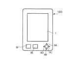
図1は、一実施形態に係る電子機器1000の外観を示した図である。電子機器1000は、画像を表示する表示装置を有する。この例で、電子機器1000は、電子書籍(文書の一例)を閲覧するための装置、いわゆる電子ブックリーダーである。電子書籍は複数ページの画像を含むデータである。電子機器1000は、電子書籍をある単位(例えば1ページずつ)で表示部1に表示する。電子書籍に含まれる複数ページのうち、表示の対象となる一のページを、「選択ページ」という。選択ページは、ユーザーによるボタン9A〜9Fの操作に応じて変更される。すなわち、ユーザーは、ボタン9A〜9Fの操作により、電子書籍のページをめくること(ページ送りまたはページ戻し)ができる。
1. Configuration FIG. 1 is a diagram illustrating an appearance of an
図2は、電子機器1000のハードウェア構成を示すブロック図である。電子機器1000は、表示部1と、コントローラー2と、制御部3と、VRAM(Video Random Access Memory)4と、RAM(Random Access Memory)5と、記憶部8と、操作部9と、バスBUSとを有する。表示部1は、画像を表示する表示素子を含むディスプレイパネルを有する。この例で、表示素子は、電圧の印加等によりエネルギーを与えなくても表示を保持するメモリー性の表示素子として、電気泳動粒子を用いた表示素子を有する。この表示素子により、表示部1は、モノクロ複数階調(この例では白黒2階調)の像を表示する。コントローラー2は、表示部1を制御する。制御部3は、電子機器1000の各部を制御する装置、例えば、CPU(Central Processing Unit)、ROM(Read Only Memory)、およびRAMを有するマイクロコンピュータである。CPUは、RAMをワークエリアとして、ROMまたは記憶部8に記憶されたプログラムを実行する。VRAM4は、表示部1に表示させる画像を示す画像データを記憶するメモリーである。RAM5は、データを記憶するメモリーであり、この例では特に、書込データを記憶する書込データ記憶領域51、予定画像データを記憶する予定画像データ記憶領域52、および2値化後の画像データを記憶する2値化データ記憶領域53とを有する。書込データおよび予定画像データの詳細は後述する。記憶部8は、電子書籍のデータ(書籍データ)を記憶する不揮発性のメモリーである。記憶部8は、複数の電子書籍のデータを記憶することができる。操作部9は、ユーザーの指示を入力するための入力装置であり、例えば、タッチスクリーン、キーパッド、またはボタンを含む。図1に示したボタン9A〜9Fは、操作部9の具体例の一つである。バスBUSは、構成要素間でデータまたは信号を伝送する伝送路である。
FIG. 2 is a block diagram illustrating a hardware configuration of the
図3は、表示部1の断面構造を示す模式図である。表示部1は、第1基板100と、電気泳動層110と、第2基板120とを有する。第1基板100および第2基板120は、電気泳動層110を挟持するための基板である。
FIG. 3 is a schematic diagram showing a cross-sectional structure of the
第1基板100は、基板101と、接着層102と、回路層103とを有する。基板101は、絶縁性及び可撓性を有する材料、例えばポリカーボネートで形成されている。基板101は、軽量性、可撓性、弾性及び絶縁性を有するものであれば、ポリカーボネート以外の樹脂材料により形成されてもよい。別の例で、基板101は、可撓性を有しないガラスにより形成されていてもよい。接着層102は、基板101と回路層103とを接着する層である。回路層103は、電気泳動層110を駆動するための回路を有する層である。回路層103は、画素電極104を有する。
The
電気泳動層110は、バインダー112と、マイクロカプセル111とを有する。マイクロカプセル111は、バインダー112によって固定されている。バインダー112としては、マイクロカプセル111との親和性が良好で電極との密着性が優れ、かつ絶縁性を有する材料が用いられる。マイクロカプセル111は、内部に分散媒および電気泳動粒子が格納されたカプセルである。マイクロカプセル111は、柔軟性を有する材料、例えばアラビアゴム・ゼラチン系の化合物またはウレタン系の化合物等が用いられる。なお、マイクロカプセル111と画素電極104との間には、接着剤により形成された接着層が設けられてもよい。
The
分散媒は、水、アルコール系溶媒(メタノール、エタノール、イソプロパノール、ブタノール、オクタノール、メチルセルソルブなど)、エステル類(酢酸エチル、酢酸ブチルなど)、ケトン類(アセトン、メチルエチルケトン、メチルイソブチルケトンなど)、脂肪族炭化水素(ぺンタン、ヘキサン、オクタンなど)、脂環式炭化水素(シクロへキサン、メチルシクロへキサンなど)、芳香族炭化水素(ベンゼン、トルエン、長鎖アルキル基を有するベンゼン類(キシレン、ヘキシルベンゼン、ヘブチルベンゼン、オクチルベンゼン、ノニルベンゼン、デシルベンゼン、ウンデシルベンゼン、ドデシルベンゼン、トリデシルベンゼン、テトラデシルベンゼンなど))、ハロゲン化炭化水素(塩化メチレン、クロロホルム、四塩化炭素、1,2−ジクロロエタンなど)、またはカルボン酸塩である。別の例で、分散媒は、その他の油類であってもよい。また、分散媒は、これらの物質が混合されたものでもよい。さらに別の例で、分散媒には、界面活性剤などが配合されてもよい。 Dispersion media include water, alcohol solvents (methanol, ethanol, isopropanol, butanol, octanol, methyl cellosolve, etc.), esters (ethyl acetate, butyl acetate, etc.), ketones (acetone, methyl ethyl ketone, methyl isobutyl ketone, etc.), Aliphatic hydrocarbons (pentane, hexane, octane, etc.), alicyclic hydrocarbons (cyclohexane, methylcyclohexane, etc.), aromatic hydrocarbons (benzene, toluene, benzenes with long chain alkyl groups (xylene, Hexylbenzene, hebutylbenzene, octylbenzene, nonylbenzene, decylbenzene, undecylbenzene, dodecylbenzene, tridecylbenzene, tetradecylbenzene)), halogenated hydrocarbons (methylene chloride, chloroform, carbon tetrachloride, 1, - dichloroethane), or a carboxylic acid salt. In another example, the dispersion medium may be other oils. The dispersion medium may be a mixture of these substances. In still another example, a surfactant or the like may be added to the dispersion medium.
電気泳動粒子は、分散媒中で電界によって移動する性質を有する粒子(高分子またはコロイド)である。本実施形態においては白の電気泳動粒子と黒の電気泳動粒子がマイクロカプセル111内に格納されている。黒の電気泳動粒子は、例えば、アニリンブラックやカーボンブラック等の黒色顔料を含む粒子であり、本実施形態では正に帯電されている。白の電気泳動粒子は、例えば、二酸化チタンや酸化アルミニウム等の白色顔料を含む粒子であり、本実施形態では負に帯電されている。
Electrophoretic particles are particles (polymer or colloid) having the property of moving by an electric field in a dispersion medium. In the present embodiment, white electrophoretic particles and black electrophoretic particles are stored in the
第2基板120は、フィルム121と、透明電極122とを有する。フィルム121は、電気泳動層110の封止および保護をするものである。フィルム121は、透明で絶縁性を有する材料、例えばポリエチレンテレフタレートにより形成される。透明電極122は、透明で導電性を有する材料、例えば酸化インジウムスズ(Indium Tin Oxide、ITO)により形成される。
The
図4は、表示部1の回路の構成を示す図である。表示部1は、m本の走査線11と、n本のデータ線12と、m×n個の画素13と、走査線駆動回路15と、データ線駆動回路16とを有する。m×n個の画素13により、表示領域14が形成される。走査線駆動回路15およびデータ線駆動回路16は、コントローラー2により制御される。走査線11は、行方向(x方向)に沿って配置されており、走査信号を伝達する。走査信号は、m本の走査線11の中から一の走査線11を順次排他的に選択する信号である。データ線12は、列方向(y方向)に沿って配置されており(延在しており)、データ信号を伝達する。データ信号は、各画素の階調に応じた信号である。走査線11とデータ線12とは絶縁されている。画素13は、走査線11およびデータ線12の交差に対応して設けられており、データ信号に応じた階調を示す。なお、複数の走査線11のうち一の走査線11を他と区別する必要があるときは、第1行、第2行、・・・、第m行の走査線11という。データ線12についても同様である。
FIG. 4 is a diagram illustrating a circuit configuration of the
図5は画素13の等価回路を示す図である。画素13は、トランジスター134と、保持容量135と、画素電極104と、電気泳動層110と、透明電極122とを有する。トランジスター134は、画素電極104へのデータの書き込みを制御するスイッチング素子、例えばnチャネルのTFT(Thin Film Transistor)である。トランジスター134のゲート、ソース、およびドレインはそれぞれ、走査線11、データ線12、および画素電極104に接続されている。L(Low)レベルの走査信号(非選択信号)がゲートに入力されているとき、トランジスター134のソースとドレインは絶縁する。H(High)レベルの走査信号(選択信号)がゲートに入力されると、トランジスター134のソースとドレインは導通し、画素電極104にデータ電圧(データ信号が示す電圧)が書き込まれる。また、トランジスター134のドレインには保持容量135も接続されている。保持容量135は、データ電圧に応じた電荷を保持する。画素電極104は、画素13に一つずつ設けられており、透明電極122と対向している。透明電極122は、すべての画素13に共通であり、電位Vcomが与えられる。画素電極104と透明電極122との間には電気泳動層110が挟まれている。電気泳動層110には、画素電極104と透明電極122との電位差に相当する電圧が印加される。マイクロカプセル111において、電気泳動層110に印加されている電圧に応じて電気泳動粒子が移動し、階調表現をする。透明電極122の電位Vcomに対して画素電極104の電位が正(例えば+15V)である場合、負に帯電している白の電気泳動粒子が画素電極104側に移動し、正に帯電している黒の電気泳動粒子が透明電極122側に移動する。このとき第2基板120側から表示部1を見ると、画素が黒に見える。透明電極122の電位Vcomに対して画素電極104の電位が負(例えば−15V)である場合、正に帯電している黒の電気泳動粒子が画素電極104側に移動し、負に帯電している白の電気泳動粒子が透明電極122側に移動する。このとき、画素が白に見える。
FIG. 5 is a diagram showing an equivalent circuit of the
なお、以下の説明においては、走査線駆動回路15が第1行の走査線を選択してから第m行の走査線の選択が終了するまでの期間を「フレーム期間」または単に「フレーム」という。各走査線11は、1フレームに一回づつ選択され、各画素13には1フレームに一回づつデータ信号が供給される。
In the following description, the period from when the scanning
図6は、コントローラー2の機能構成を示す図である。コントローラー2は、出力部251と、制御部252と、減色処理部253と、記憶部254とを有する。出力部251は、表示部1(電気光学装置)を制御するための信号を表示部1に(より具体的には、走査線駆動回路15およびデータ線駆動回路16に)出力する。制御部252は。VRAM4に記憶されているデータに応じた電圧をデータ線12に印加させるための信号を出力するように出力部251を制御する。ここでは、第1条件が満たされたときにこの信号により書き込まれる画像が、第2条件が満たされたときにこの信号により書き込まれる画像よりも、データ線12の延在方向における階調変化の空間周波数が高い。減色処理部253は、VRAM4に記憶されているデータにより示される、m行n列の画素13の各々における階調値に対して減色処理をする。第1条件が満たされたときの減色処理により得られる画像は、第2条件が満たされたときの減色処理により得られる画像よりも、データ線12の延在方向における空間周波数が高い。記憶部254は、ベイヤー型ディザマトリクス(第1ディザマトリクスの一例)および縦型ディザマトリクス(第2ディザマトリクスの一例)を記憶している。減色処理部253は、第1条件が満たされたときは第1ディザマトリクスを用い、第2条件が満たされたときは第2ディザマトリクスを用いて減色処理を行う。これらの機能は、ハードウェアにより実現される。別の例で、コントローラー2がプロセッサを有し、プログラムを実行することによりこれらの機能を実現してもよい。
FIG. 6 is a diagram illustrating a functional configuration of the
2.動作
図7は、電子機器1000の動作を示すフローチャートである。図7のフローは、例えば、ある電子書籍を表示する指示をユーザーが電子機器1000に入力したことを契機として開始される。ステップS100において、制御部3は、表示される電子書籍を特定する。また、制御部3は、この電子書籍に含まれる複数のページの中から、一のページを選択ページとして選択する。表示される電子書籍および選択ページは、例えばユーザーの指示に応じて特定される。
2. Operation FIG. 7 is a flowchart showing the operation of the
ステップS110において、制御部3は、対象となる電子書籍の書籍データから、選択ページのデータを取得する。制御部3は、取得したデータから、m行n列の画素13の各々における階調値を示すラスターデータを生成する。制御部3は、生成したラスターデータをVRAM4に書き込む。VRAM4にデータを書き込むと、制御部3は、コントローラー2に対して画像書き替えの指示をする。制御部3からの指示を受けると、コントローラー2は、画像の書き替えを行う。書き替え動作の詳細は後述する。
In step S <b> 110, the
ステップS120において、コントローラー2は、画像書き替えの指示があったか判断する。画像書き替えの指示は、制御部3から出力される。制御部3は、ユーザーの指示に応じて、例えば、ユーザーがページ送りのボタン9を押下して選択ページを変更する指示を入力すると、VRAM4を書き替えた後、画像書き替えの指示を出力する。画像書き替えの指示があった場合(ステップS120:YES)、コントローラー2は、処理をステップS130に移行する。画像書き替えの指示がなかった場合(ステップS120:NO)、コントローラー2は、画像書き替えの指示があるまで待機する。
In step S120, the
ステップS130において、コントローラー2は、書き替え指示が、第1条件および第2条件を含む複数の条件のうちどの条件を満たしているか判断する。この例では、第1条件として、高速のページ送りが行われているという条件が、第2条件として、通常のページ送りが行われているという条件が用いられる。「高速のページ送り」とは、直近の書き替え指示が入力された時刻から、新たな書き替え指示が入力されるまでの時間がしきい値以下であるような書き替え指示が入力されたことをいう。「通常のページ送り」とは、高速のページ送りではないページ送り、すなわち、直近の書き替え指示が入力された時刻から、新たな書き替え指示が入力されるまでの時間がしきい値より長いような書き替え指示が入力されたことをいう。この場合、コントローラー2は、直近の書き替え指示があった時刻をRAM5に記憶している。第1条件が満たされたと判断した場合(ステップS130:A)、コントローラー2は、処理をステップS140に移行する。第2条件が満たされたと判断した場合(ステップS130:B)、コントローラー2は、処理をステップS150に移行する。
In step S <b> 130, the
この例で、コントローラー2は、第1動作モードおよび第2動作モードを含む複数の動作モードのうち、いずれか一の動作モードに従って減色処理を行う。「減色処理」とは、p階調のデータをq階調のデータに変換する処理(p>q)をいう。この例で、コントローラー2は、減色処理の一例として、ディザマトリクス(ディザパターンまたはディザテーブルともいう)を用いてデータを2値化する、パターンディザ法を用いた2値化処理を行う。
In this example, the
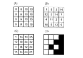
図8は、パターンディザ法を説明する図である。ここでは、0から15の16階調の元データを、0から1の2階調のデータに変換する例を説明する。簡単のため、画像データが4行4列の画素により構成され、ディザマトリクスが4行4列のマトリクスである例を用いる。図8(A)は、元データを例示する図である。この例で、元データにおいて、第1列〜第4列の階調値は、それぞれ、「0」、「5」、「10」、および「15」である。図8(B)は、ディザマトリクスを例示する図である。図8(B)は、いわゆるベイヤー(Bayer)型のディザマトリクスを示している。ディザマトリクスにおいて、基本的には、階調値に相当する数値(0〜15の16個の数値。以下「ディザ値」という)が、ある規則に従って配置されている。なお、図8(B)の例では、ディザ値「0」は使用されておらず、1〜15の15個の数値が用いられている。このため、中間階調に相当するディザ値「8」がディザマトリクスにおいて2回登場している。 FIG. 8 is a diagram for explaining the pattern dither method. Here, an example in which original data of 16 gradations from 0 to 15 is converted into data of 2 gradations from 0 to 1 will be described. For simplicity, an example in which the image data is composed of pixels of 4 rows and 4 columns and the dither matrix is a matrix of 4 rows and 4 columns is used. FIG. 8A is a diagram illustrating original data. In this example, in the original data, the gradation values of the first column to the fourth column are “0”, “5”, “10”, and “15”, respectively. FIG. 8B is a diagram illustrating a dither matrix. FIG. 8B shows a so-called Bayer type dither matrix. In the dither matrix, basically, numerical values corresponding to gradation values (16 numerical values from 0 to 15, hereinafter referred to as “dither values”) are arranged according to a certain rule. In the example of FIG. 8B, the dither value “0” is not used, and 15 numerical values of 1 to 15 are used. For this reason, the dither value “8” corresponding to the intermediate gradation appears twice in the dither matrix.
ディザマトリクスを用いた2値化処理は以下のように行われる。まず、元データの階調値と、ディザマトリクスのディザ値とが加算される。加算は、対応する画素およびセルについて行われる。例えば、元データにおける第i行第j列の画素の階調値と、ディザマトリクスにおける第i行第j列のセルのディザ値とが加算される。図8(C)は、両者が加算された状態を示している。次に、この加算値に対し、しきい値を基準として2値化が行われる。しきい値としては、階調数に応じた数値、この例では「16」が用いられる。すなわち、加算値が16未満である画素の階調値は「0」に変換され、加算値が16以上である画素の階調値は「1」に変換される。図8(D)は、2値化後の状態を示している。なお、ディザマトリクスにおいてディザ値「0」が用いられていない理由は、階調値「15」の画素については、加算値が必ずしきい値以上となるようにするためである。仮に、階調値「15」の画素にディザ値「0」が加算された場合を考えると、加算値は「15」でありしきい値以上とならず、最大階調値を有する画素の階調が「0」に変換される可能性が生じてしまう。このような事態を避けるため、ディザ値「0」は用いられていない。 The binarization process using the dither matrix is performed as follows. First, the gradation value of the original data and the dither value of the dither matrix are added. The addition is performed for the corresponding pixel and cell. For example, the gradation value of the pixel in the i-th row and j-th column in the original data and the dither value of the cell in the i-th row and j-th column in the dither matrix are added. FIG. 8C shows a state in which both are added. Next, this added value is binarized with reference to a threshold value. As the threshold value, a numerical value corresponding to the number of gradations, “16” in this example, is used. That is, the gradation value of a pixel having an addition value less than 16 is converted to “0”, and the gradation value of a pixel having an addition value of 16 or more is converted to “1”. FIG. 8D shows a state after binarization. The reason why the dither value “0” is not used in the dither matrix is to ensure that the added value is always equal to or greater than the threshold value for the pixel having the gradation value “15”. If the dither value “0” is added to the pixel having the gradation value “15”, the addition value is “15” and does not exceed the threshold value. There is a possibility that the key is converted to “0”. In order to avoid such a situation, the dither value “0” is not used.
図8では、説明を簡単にするため、元データの画素数とディザマトリクスのセル数が同じである例を用いて説明した。しかし、両者は異なっていてもよい。例えば、800行480列の画素からなる画像を、16行16列のセルからなるディザマトリクスを用いて2値化する場合、元データの画像は16行16列のブロックに区分され、各ブロックにおいて上述の処理が行われる。 In FIG. 8, in order to simplify the description, an example in which the number of pixels of the original data and the number of cells of the dither matrix are the same is described. However, they may be different. For example, when binarizing an image composed of pixels of 800 rows and 480 columns using a dither matrix composed of cells of 16 rows and 16 columns, the image of the original data is divided into blocks of 16 rows and 16 columns. The above processing is performed.
本実施形態において、コントローラー2は、第1ディザマトリクスおよび第2ディザマトリクスを含む複数のディザマトリクスを内部メモリーに記憶している。コントローラー2は、第1動作モードにおいては第1ディザマトリクスを、第2動作モードにおいては第2ディザマトリクスを用いて2値化処理を行う。この例では、第1ディザマトリクスとしてベイヤー型のディザマトリクスが、第2ディザマトリクスとして縦型のディザマトリクスが用いられる。縦型のディザマトリクスは、低消費電力型のディザマトリクスの一例である。ここで、「低消費電力型のディザマトリクス」とは、第1ディザマトリクスと比較して、データ線12の延在方向に相当する方向(図中列方向すなわち縦方向)の階調値の変化の空間周波数が低いディザマトリクスをいう。
In the present embodiment, the
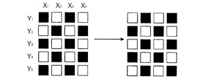
図9は、低省電力型のディザマトリクスを例示する図である。図9(A)はベイヤー型のディザマトリクスを、図9(B)は低消費電力型のディザマトリクスを示している。図9(C)は、すべての画素の階調値が「8」(中間階調値)であるデータを図9(A)のディザマトリクスを用いて2値化処理した処理後の画像を、図9(D)は同じデータを図9(B)のディザマトリクスを用いて2値化処理した処理後の画像を、それぞれ示している。図9(C)と図9(D)とを比較するとわかるように、低消費電力型のディザマトリクスを用いて2値化処理した画像の方が、列方向の階調変化の空間周波数が低い。すなわち、低消費電力型のディザマトリクスを用いて2値化処理した画像の方が、列方向に同じ階調値が連続しているしている割合が高い。 FIG. 9 is a diagram illustrating a low power saving type dither matrix. 9A shows a Bayer type dither matrix, and FIG. 9B shows a low power consumption type dither matrix. FIG. 9C shows a processed image obtained by binarizing data in which the gradation value of all pixels is “8” (intermediate gradation value) using the dither matrix of FIG. FIG. 9D shows images after processing that binarizes the same data using the dither matrix of FIG. 9B. As can be seen by comparing FIG. 9C and FIG. 9D, the spatial frequency of gradation change in the column direction is lower in the image binarized using the low power consumption type dither matrix. . In other words, an image binarized using a low power consumption type dither matrix has a higher ratio of the same gradation values in the column direction.
再び図7を参照する。ステップS140において、コントローラー2は、第1動作モードで2値化処理(減色処理)を行う。コントローラー2は、2値化した画像データを、RAM5の2値化データ記憶領域53に書き込む。ステップS160において、コントローラー2は、画素13に対する書き込み動作を行う。
Refer to FIG. 7 again. In step S140, the
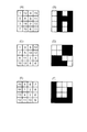
図10は、第1動作モードにおいて書き込まれる画像を例示する図である。図10(A)は書き替え前の画像を、図10(B)は書き替え後の画像を示している。説明を簡単にするため、5行4列の画素のみを示している。第1動作モードにおいては空間周波数の高いディザマトリクスを用いて2値化処理が行われるので、書き替え前後で階調値が異なる場合において、ある列に着目したときに階調変化の頻度が高くなるときがある。図10は最も分かりやすい例を示している。この例では、5行4列のすべての画素の階調が変更され、かつ、変更後の階調は、列方向において白と黒が1画素ずつ交互に出現している。 FIG. 10 is a diagram illustrating an image written in the first operation mode. FIG. 10A shows an image before rewriting, and FIG. 10B shows an image after rewriting. For simplicity of explanation, only the pixels in 5 rows and 4 columns are shown. In the first operation mode, the binarization process is performed using a dither matrix having a high spatial frequency. Therefore, when the gradation values are different before and after rewriting, the frequency of gradation change is high when attention is paid to a certain column. There are times when FIG. 10 shows the most easily understood example. In this example, the gradation of all the pixels in 5 rows and 4 columns is changed, and in the gradation after the change, white and black appear alternately one pixel at a time in the column direction.
図11は、図10の例において走査線11およびデータ線12に供給される信号を例示する図である。あるフレームにおいて、第1行から第5行の走査線11が順次排他的に選択される。列方向(縦方向)に隣接する画素の階調が1画素ずつ変化しているので、データ線12に供給される信号は、1水平期間ごとに30Vの振幅で電圧が変化する信号である。データ線12は寄生容量を有しているので、このように高い周波数で電圧が変化すると、低周波数で電圧が変化する場合と比較してより高い電力を消費する。
FIG. 11 is a diagram illustrating signals supplied to the
再び図7を参照する。ステップS150において、コントローラー2は、第2動作モードで2値化処理(減色処理)を行う。コントローラー2は、2値化した画像データを、RAM5の2値化データ記憶領域53に書き込む。ステップS160において、コントローラー2は、画素13に対する書き込み動作を行う。
Refer to FIG. 7 again. In step S150, the
図12は、第2動作モードにおいて書き込まれる画像を例示する図である。図12(A)は書き替え前の画像を、図12(B)は書き替え後の画像を示している。第2動作モードにおいては、第1動作モードよりも空間周波数の低いディザマトリクスを用いて2値化処理が行われるので、書き替え前後で階調値が異なる画素の割合は第1動作モードよりも小さい。また、書き替え前後で階調値が異なる場合において、ある列に着目したときの階調変化の頻度は、第1動作モードよりも低い。 FIG. 12 is a diagram illustrating an image written in the second operation mode. FIG. 12A shows an image before rewriting, and FIG. 12B shows an image after rewriting. In the second operation mode, since the binarization process is performed using a dither matrix having a lower spatial frequency than in the first operation mode, the ratio of pixels having different gradation values before and after rewriting is higher than that in the first operation mode. small. In addition, when the gradation values are different before and after rewriting, the frequency of gradation change when focusing on a certain column is lower than in the first operation mode.
図13は、図12の例において走査線11およびデータ線12に供給される信号を例示する図である。例えば第1列の画素13についてみると、第1行、第4行および第5行は階調が変更されず、第2行および第3行は、黒から白へ階調が変更される。この間、第1列のデータ線12に供給される信号の電圧は、2回しか変化しておらず、振幅は15Vである。図11の第1動作モードの例(第1列のデータ線12に供給される信号の電圧が6回変化しており、その振幅が30Vである)と比較して、消費電力が低いのは明らかである。
FIG. 13 is a diagram illustrating signals supplied to the
次に、ステップS110およびS160等における画像の書き込み動作の詳細を説明する。電子機器1000において、白(低濃度または低階調)から黒(高濃度または高階調)または黒から白への、画素の表示状態は、複数フレームに渡る電圧の印加(電荷の蓄積)により変化する。すなわち、1フレームだけの電圧の印加では、画素は所望の表示状態にはならない。
Next, details of the image writing operation in steps S110 and S160 will be described. In the
図14は、コントローラー2の機能構成を示すブロック図である。コントローラー2は、書き替え判断部201と、書込状態判断部202と、書込制御部203と、データ更新部204と、予定画像更新部205とを有する。これらの機能は、ハードウェアにより実現される。別の例で、コントローラー2にプロセッサーを設け、このプロセッサーがプログラムを実行することにより各ブロックが実現されてもよい。コントローラー2は、図6で説明した機能に加えて、これらの機能を有している。
FIG. 14 is a block diagram illustrating a functional configuration of the
書き替え判断部201は、2値化データ記憶領域53に記憶されている画像データと、予定画像データ記憶領域52に記憶されている画像データとを比較し、両者が異なるか否か判断する。書込状態判断部202は、書込データ記憶領域51に記憶されているデータを参照し、画素を黒から白または白から黒へ変化させるための書き替え動作が進行中か否か判断する。書込データ記憶領域51は、各画素について黒から白へ表示状態を変更する動作が進行中であるか否かを示すデータ(第1書込データ)を記憶する白書込データ記憶領域51Aと、各画素について白から黒へ表示状態を変更する動作が進行中であるか否かを示すデータ(第2書込データ)を記憶する黒書込データ記憶領域51Bとを有する。
The
書込制御部203は、所望の画素の画素電極104に対してデータ信号が供給されるように走査線駆動回路15とデータ線駆動回路16を制御する。データ更新部204は、白書込データ記憶領域51Aと黒書込データ記憶領域51Bにデータを書き込む。予定画像更新部205は、予定画像データ記憶領域52に記憶されている画像データを2値化データ記憶領域53に記憶されている画像データで上書きする。
The
図15は、コントローラー2による表示部1の駆動処理を示すフローチャートである。以下において、表示部1における第i行第j列の画素を、画素Pijという。2値化データ記憶領域53において、画素Pijの階調を示すデータを記憶する領域を、記憶領域Aijという。この例で、記憶領域Aijに記憶されるデータは、0(黒)または7(白)の2値である。予定画像データ記憶領域52において、画素Pijの予定画像データを記憶する領域を、記憶領域Bijという。予定画像データとは、進行中の書き込み処理が終了したときの表示部1の状態を示すデータをいう。この例で、記憶領域Bijに記憶されるデータは、0(黒)または7(白)の2値である。書込データ記憶領域51は、白書込データ記憶領域51Aおよび黒書込データ記憶領域51Bとを有する。白書込データ記憶領域51Aは、第1書込データとして階調を黒から白に書き替える画素における残り電圧印加回数を記憶する。黒書込データ記憶領域51Bは、第2書込データとして階調を白から黒に書き替える画素における残り電圧印加回数を記憶する。白書込データ記憶領域51Aにおいて、画素Pijの残り電圧印加回数を示すデータを記憶する領域を、記憶領域Cijという。黒書込データ記憶領域51Bにおいて、画素Pijの残り電圧印加回数を示すデータを記憶する領域を、記憶領域Dijという。
FIG. 15 is a flowchart showing the driving process of the
ステップS11およびS12において、書込状態判断部202は、変数iおよびjの値を初期化する。この例では、変数iおよびjは、i=1およびj=1に初期化される。ステップS13において、書込状態判断部202は、変数iおよびjで特定される画素Pijを選択する。例えば、変数iの値が1であり、変数jの値が1である場合、画素P11が選択される。
In steps S11 and S12, writing
ステップS14において、書込状態判断部202は、記憶領域Cijに記憶されている第1書込データと、記憶領域Dijに記憶されている第2書込データの両方が0であるか判断する。すなわち、書込状態判断部202は、画素Pijについて書き込み処理が継続中ではないか判断する。画素Pijについて第1書込データと第2書込データの両方が0である場合(ステップS14:YES)、書込状態判断部202は、処理をステップS16に移行する。画素Pijについて第1書込データおよび第2書込データの一方が0でない場合(ステップS14:NO)、書込状態判断部202は、処理をステップS15に移行する。
In step S14, the write
ステップS15において、データ更新部204は、第1書込データおよび第2書込データのうち、値が0以外のデータから1を減算する。なお、第1書込データおよび第2書込データのうち、値が0のデータについては、データ更新部204は、1を減算しない。ステップS19において、データ更新部204は、変数jの値がデータ線の本数nと同じであるか否か判断する。変数jの値がnでない場合(ステップS19:NO)、データ更新部204は、変数jの値に1を加える(ステップS20)。変数jの値に1を加えると、データ更新部204は、処理をステップS13に移行する。変数jの値がnである場合(ステップS19:YES)、データ更新部204は、処理をステップS21に移行する。ステップS21において、データ更新部204は、変数iの値が走査線の本数mと同じであるか判断する。変数iの値がmでない場合(ステップS21:NO)、データ更新部204は、変数iの値に1を加える(ステップS22)。変数iの値に1を加えると、データ更新部204は、処理をステップS12へ移行する。変数iの値がmである場合(ステップS21:YES)、データ更新部204は、処理をステップS23に移行する。ステップS23において、書込制御部203は、走査線駆動回路15とデータ線駆動回路16とを制御して画素駆動回路を駆動する。
In step S15, the
ステップS16(判断工程)において、書き替え判断部201は、記憶領域Aijに記憶されているデータと、記憶領域Bijに記憶されているデータとが同じであるか判断する。これらのデータが異なっている場合(ステップS16:NO)、書き替え判断部201は、処理をステップS17に移行する。
In step S16 (determination step), the
ステップS17(データ更新工程)において、データ更新部204は、画素Pijの階調を記憶領域Aijの階調に変更するまでに必要な画素への電圧の印加回数を書込データ記憶領域51に書き込む。ステップS18において、予定画像更新部205は、記憶領域Bijの内容を記憶領域Aijに記憶されている内容で上書きする。
In step S <b> 17 (data update process), the
図16は、メモリーに記憶されているデータを例示する図である。ここでは、表示部1の一部である4行4列の画素P11〜P44を例として説明する。この例では、画素の階調は0〜7の8段階で表される。階調7は白に、階調0は黒にそれぞれ対応している。図面を見やすくするため画素に数値が記載されているが、この数字が表示されているわけではない。図16の例では、画素P11、P12、P21、およびP22は黒であり、それ以外の画素は白である。書き込みが進行中の画素はなく、すべての画素について書き込みは完了した状態である。
FIG. 16 is a diagram illustrating data stored in the memory. Here, description will be given by taking, as an example, pixels P11 to P44 of 4 rows and 4 columns, which are a part of the
図17は、2値化データ記憶領域53の書き替えが行われた状態を例示する図である。この例では、画素P33、P34、P43、およびP44が黒であり、それ以外の画素は白である。2値化データ記憶領域53の書き替え、すなわち、2値化データ記憶領域53へのデータの書き込み(データ書き込み工程)は、制御部3により行われる。いま、図17の状態でステップS13において画素P11が選択された場合を例として説明する。この場合、記憶領域C11およびD11に記憶されているデータは共に0なので、ステップS14における判断結果はYESである。次に、記憶領域A11のデータと記憶領域B11のデータとは同じでないので、ステップS16における判断結果はNOである。ステップS17において、記憶領域C11に、記憶領域B11のデータが書き込まれる。ステップS18において、記憶領域B11に記憶領域A11のデータが書き込まれる。
FIG. 17 is a diagram illustrating a state where the binarized
図18は、記憶領域B11のデータが書き替えられた状態を例示する図である。次に、対象となる画素が画素P12に更新される。記憶領域C12およびD12に記憶されているデータは共に0なので、ステップS14における判断結果はYESである。次に、記憶領域A12のデータと記憶領域B12のデータとは同じでないので、ステップS16における判断結果はNOである。ステップS17において、記憶領域C12に、電圧印加回数(この例では7回)を示すデータが書き込まれる。ステップS18において、記憶領域B12に記憶領域A12のデータが書き込まれる。 FIG. 18 is a diagram illustrating a state in which the data in the storage area B11 has been rewritten. Next, the target pixel is updated to the pixel P12. Since the data stored in the storage areas C12 and D12 are both 0, the determination result in step S14 is YES. Next, since the data in the storage area A12 and the data in the storage area B12 are not the same, the determination result in step S16 is NO. In step S17, data indicating the number of times of voltage application (in this example, 7 times) is written in the storage area C12. In step S18, the data in the storage area A12 is written into the storage area B12.
図19は、記憶領域B12のデータが書き替えられた状態を例示する図である。同様にして処理が画素P44まで進むと、予定画像データ記憶領域52に記憶されているデータは2値化データ記憶領域53に記憶されているデータと同じになる。
FIG. 19 is a diagram illustrating a state where the data in the storage area B12 has been rewritten. Similarly, when the process proceeds to the pixel P44, the data stored in the scheduled image
図20は、すべての画素についてデータが書き替えられた状態を例示する図である。黒から白に階調を書き替える画素については、記憶領域Cij(C11、C12、C21、およびC22)に記憶されているデータが「7」になっている。白から黒に階調を書き替える画素については、記憶領域Dij(D33、D34、D43、およびD44)に記憶されているデータが「7」になっている。記憶領域CijおよびDijにおいて、それ以外の画素についてのデータは「0」になっている。 FIG. 20 is a diagram illustrating a state in which data has been rewritten for all pixels. For the pixel whose gradation is rewritten from black to white, the data stored in the storage area Cij (C11, C12, C21, and C22) is “7”. For the pixel whose gradation is rewritten from white to black, the data stored in the storage area Dij (D33, D34, D43, and D44) is “7”. In the storage areas Cij and Dij, the data for the other pixels is “0”.
データの書き替えが終わると、書込制御部203は表示部1を駆動する。第i行の走査線が選択されたときに、記憶領域Cijのデータが0以外である画素については、透明電極122の電位Vcomを基準として画素電極104の電位が低くなる電圧を印加させる制御を、書込制御部203が行う。記憶領域Dijのデータが0以外である画素については、透明電極122の電位Vcomを基準として画素電極104の電位(以下、透明電極122の電位Vcomを基準とした、画素電極104と透明電極122と電位差を単に「画素の電圧」という)が高くなる電圧を印加させる制御を、書込制御部203が行う。例えば、画素P11については、記憶領域C11に記憶されているデータが0ではない。したがって、第1行の走査線が選択されたとき、第1列のデータ線には画素の電圧を−15Vとする電圧が印加される。別の例で、画素P33については、記憶領域D33に記憶されているデータが0ではない。したがって、第3行の走査線が選択されたとき、第3列のデータ線には画素の電圧を+15Vとする電圧が印加される。さらに、記憶領域Cijのデータも記憶領域Dijのデータも0である画素Pijに対しては、画素の電圧を0Vとする電圧が第j行のデータ線に印加される。
When the data rewriting is finished, the
図21は、図20の状態から1フレームの電圧印加後の状態を例示する図である。表示部1の画素において、荷電粒子が移動したことにより階調が変化している。この例では、画素P11、P12、P21、およびP22が黒から1フレームの電圧印加分明るい階調になり、画素P33、P34、P43、およびP44が白から1フレームの電圧印加分暗い階調になっている。
FIG. 21 is a diagram illustrating a state after voltage application of one frame from the state of FIG. In the pixel of the
1フレームの電圧印加が修了すると、コントローラー2における処理は、再びステップS11から繰り返される。図21の状態でステップS13において画素P11が選択された場合、記憶領域C11に記憶されているデータは0ではないので、ステップS14における判断結果はNOである。ステップS15において、記憶領域C11に記憶されているデータ(0ではないデータ)から1が減算され、記憶領域C11のデータは6になる。同様にして、すべての画素について記憶領域のデータが書き替えられる。
When the voltage application for one frame is completed, the processing in the
図22は、すべての画素について書込データ記憶領域のデータの書き替えが終了した状態を例示する図である。図21の状態と比較すると、記憶領域C11、C12、C21、およびC22のデータ、並びに記憶領域D33、D34、D43、およびD44のデータが6になっている点が異なっている。 FIG. 22 is a diagram illustrating a state in which rewriting of data in the write data storage area is completed for all pixels. Compared to the state of FIG. 21, the data in the storage areas C11, C12, C21, and C22 and the data in the storage areas D33, D34, D43, and D44 are different.
図23は、図22に示した状態から2回目のステップS23の処理が行われた直後の状態を示した図である。図22の状態と比較すると、記憶領域C11、C12、C21、およびC22のデータ、並びに記憶領域D33、D34、D43、およびD44のデータが5になっている点が異なっている。さらに、表示部1における画素P11、P12、P21、およびP22の階調が3になっており、画素P33、P34、P43、およびP44の階調が4になっている点が図22の状態と異なっている。ここで、図23の状態のとき(2回目のステップS23の処理が行われた直後)に2値化データ記憶領域53のデータが書き替えられた場合の動作を考える。
FIG. 23 is a diagram illustrating a state immediately after the process of step S23 is performed for the second time from the state illustrated in FIG. Compared to the state of FIG. 22, the data in the storage areas C11, C12, C21, and C22 and the data in the storage areas D33, D34, D43, and D44 are different. Furthermore, the gradation of the pixels P11, P12, P21, and P22 in the
図24は、2値化データ記憶領域53のデータが書き替えられた状態を例示する図である。この例では、第1行および第4行の画素がすべて白に、第2行および第3行の画素がすべて黒である。この状態で、コントローラー2は、ステップS11からの処理を実行する。例えば、ステップS13において画素P21が選択された場合、ステップS14における判断結果はNOである。ステップS15において、記憶領域C21のデータは1が減算されて4になる。別の例で、ステップS13において画素P23が選択された場合、ステップS14における判断結果はYESである。さらに、ステップS16における判断結果葉NOである。したがって、処理はステップS17に進む。ステップS17において、記憶領域D23のデータとして7が書き込まれる。ステップS18において、記憶領域B23のデータとして、記憶領域A23のデータが書き込まれる。このように、2値化データ記憶領域53のデータが書き替えられても、書き込み動作が進行中の画素(図24の例では、画素P11、P12、P21、P22、P33、P34、P43、およびP44)については、進行中の書き込み動作(書き替えられる前の2値化データ記憶領域53のデータに基づく画素の書き込み動作)がそのまま進められる。一方、書き込み動作が進行中でない画素(画素P13、P14、P23、P24、P31、P32、P41、およびP42)については、書き替えられた2値化データ記憶領域53のデータに基づく画素の書き込み動作が行われる。
FIG. 24 is a diagram illustrating a state where data in the binarized
図25は、図24の状態からすべての画素についてデータの書き替えが終了した状態を例示する図である。図24の状態と比較すると、記憶領域B23、B24、B31、およびB32のデータが0に書き替えられている点が異なっている。また、記憶領域C11、C12、C21、C22、D33、D34、D43、およびD44のデータが4に書き替えられている点が異なっている。さらに、記憶領域D23、D24、D31、およびD32のデータが7に書き替えられている点が異なっている。 FIG. 25 is a diagram illustrating a state where data rewriting has been completed for all pixels from the state of FIG. Compared with the state of FIG. 24, the data in the storage areas B23, B24, B31, and B32 is rewritten to 0. Further, the difference is that the data in the storage areas C11, C12, C21, C22, D33, D34, D43, and D44 is rewritten to 4. Another difference is that the data in the storage areas D23, D24, D31, and D32 is rewritten to 7.
図26は、図25の状態からステップS23の処理が行われた状態を例示する図である。2値化データ記憶領域53のデータの書き替え前から既に書き込み動作が進行中であった画素(画素P11、P12、P21、P22、P33、P34、P43、およびP44)については、書き替え後の2値化データ記憶領域53のデータによらず、従前の書き込み動作が継続される。2値化データ記憶領域53のデータの書き替え後に書き替えが必要になった画素のうち、2値化データ記憶領域53のデータの書き替え前には書き込み動作が行われていなかった画素(画素P13、P14、P31、およびP32)については、書き替え後の2値化データ記憶領域53のデータに基づく画素の書き替えが開始される。
FIG. 26 is a diagram illustrating a state in which the process of step S23 has been performed from the state of FIG. For the pixels (pixels P11, P12, P21, P22, P33, P34, P43, and P44) for which the write operation has already been performed before rewriting the data in the binarized
図27は、図26からさらに書き込み動作が進められ、2値化データ記憶領域53のデータの書き替え前から既に書き込み動作が進行中であった画素(画素P11、P12、P21、P22、P33、P34、P43、およびP44)について、所定回数の電圧の印加が終了した状態を例示する図である。この状態では、書込データ記憶領域51においては、記憶領域D23、D24、D31、およびD32のデータは3であり、これ以外の記憶領域のデータは0である。表示部1において、画素P23、P24、P31、およびP32の階調は2である。画素P33、P34、P43、およびP44の階調は0である。それ以外の画素の階調は7である。この状態で、ステップS13において画素P21が選択された場合を例として考える。この場合、ステップS14における判断結果はYESである。さらに、ステップS16における判断結果はNOである。ステップS17において、記憶領域D21のデータとして7が書き込まれる。ステップS18において、記憶領域B21に記憶領域A21のデータと同じ0がデータとして書き込まれる。
In FIG. 27, the writing operation is further advanced from FIG. 26, and the pixels (pixels P <b> 11, P <b> 12, P <b> 21, P <b> 22, P <b> 33. It is a figure which illustrates the state which applied the voltage of the predetermined number of times about P34, P43, and P44). In this state, in the write
図28は、すべての画素についてデータの書き替えが完了した状態を例示する図である。図27と比較すると、記憶領域B21およびB22の値が7になっており、記憶領域B43およびB44のデータが0になっている点が異なっている。また、記憶領域C43、C44、D21、およびD22のデータが7になっている点が異なっている。さらに、記憶領域D23、D24、D31、およびD32のデータが2になっている点が異なっている。 FIG. 28 is a diagram illustrating a state where data rewriting has been completed for all pixels. Compared with FIG. 27, the values of the storage areas B21 and B22 are 7, and the data of the storage areas B43 and B44 is 0. Further, the difference is that the data in the storage areas C43, C44, D21, and D22 is 7. Further, the difference is that the data in the storage areas D23, D24, D31, and D32 is 2.
図29は、図28の状態から画素の書き替えが行われた状態を例示する図である。図28の状態と比較すると、画素P23、P24、P31、およびP32の階調が1になっている点が異なっている。また、画素P21およびP22の階調が6になっており、画素P43およびP44の階調が1になっている点が異なっている。 FIG. 29 is a diagram illustrating a state in which the pixel has been rewritten from the state of FIG. Compared with the state of FIG. 28, the difference is that the gradation of pixels P23, P24, P31, and P32 is 1. Further, the difference is that the gradation of the pixels P21 and P22 is 6, and the gradation of the pixels P43 and P44 is 1.
図30は、図29の状態から処理が1フレーム進んだ状態を例示する図である。図29の状態と比較すると、画素P23、P24、P31、およびP32の階調が0になっている点が異なっている。また、画素P21およびP22の階調が5になっており、画素P43およびP44の階調が2になっている点が異なっている。さらに、記憶領域C43、C44、D21、およびD22のデータが6になっている点が異なっている。さらに、記憶領域D23、D24、D31、およびD32のデータが1になっている点が異なっている。 FIG. 30 is a diagram exemplifying a state in which the process has advanced one frame from the state of FIG. Compared with the state of FIG. 29, the difference is that the gradations of the pixels P23, P24, P31, and P32 are zero. Further, the difference is that the gradation of the pixels P21 and P22 is 5, and the gradation of the pixels P43 and P44 is 2. Further, the difference is that the data in the storage areas C43, C44, D21, and D22 is 6. Further, the difference is that the data in the storage areas D23, D24, D31, and D32 is 1.
図31は、図30の状態から処理が進められた状態を例示する図である。この状態では、2値化データ記憶領域53のデータと表示部1の階調とが一致している。また、書込データ記憶領域に記憶されているデータはすべて0であり、すべての画素について書き込み処理が終了していることが示されている。
FIG. 31 is a diagram exemplifying a state in which the process has proceeded from the state of FIG. In this state, the data in the binarized
まとめると、表示書き込み動作において、表示部1は、複数の画素を有し、画素へ電圧を複数回印加する書き込み動作により画素の階調が変更される。この表示書き込み動作は、表示部1に新たに表示する画像を表す画像データと、進行中の書き込み動作によって表示部1に表示される予定の画像を示す予定画像データとを比較し、複数の画素において階調を変更する画素を判断するステップ(ステップS16)と、階調を変更する画素と判断された画素が書き込み動作中ではない場合には、画像データの定める階調となるようにその画素に対して書き込み動作を開始し、判断工程において階調を変更する画素と判断された画素が書き込み動作中である場合には、進行中の書き込み動作が終了した後、画像データの定める階調となるようにその画素に対して書き込み動作を開始するステップ(ステップS23)とを有する。
In summary, in the display writing operation, the
本実施形態によれば、先に書き替えが開始された領域と新たに書き替えを行う領域とが部分的に重なった場合でも、新たに書き替えを開始する時に書き替えが進行中でなかった部分については、書き替えが直ぐに開始される。したがって、ユーザーには表示速度が早く感じられる。また、本実施形態によれば、単一のフレーム内において、正電圧が印加される画素と負電圧が印加される画素を共存させることができる(このように、単一のフレームで正電圧と負電圧の両方を選択できる駆動を、「両極駆動」という)。 According to this embodiment, even when the area where rewriting has been started first and the area where rewriting is newly overlapped, rewriting was not in progress when starting a new rewriting. For the part, rewriting is started immediately. Therefore, the user can feel the display speed faster. Further, according to the present embodiment, a pixel to which a positive voltage is applied and a pixel to which a negative voltage is applied can coexist in a single frame (in this way, the positive voltage and Drive that can select both negative voltages is called "bipolar drive").
以上で説明したように、本実施形態によれば、状況に応じて第1動作モード(相対的に高消費電力)と第2動作モード(相対的に低消費電力)とが使い分けられる。第1動作モードのみ、単一の動作モードが用いられる場合と比較して、より低消費電力で、面積階調による表示を行うことができる。 As described above, according to the present embodiment, the first operation mode (relatively high power consumption) and the second operation mode (relatively low power consumption) are selectively used depending on the situation. Only in the first operation mode, display by area gradation can be performed with lower power consumption than in the case where a single operation mode is used.
3.他の実施形態
本発明は上述の実施形態に限定されるものではなく、種々の形態で実施が可能である。以下、変形例をいくつか説明する。以下の変形例のうち、2つ以上のものが組み合わせて用いられてもよい。
3. Other Embodiments The present invention is not limited to the above-described embodiments, and can be implemented in various forms. Hereinafter, some modifications will be described. Two or more of the following modifications may be used in combination.
3−1.変形例1
画像の書き込み動作は図15のフローで説明したものに限定されない。変形例1において、RAM5は、書き替え前の画像データを記憶する記憶領域と、書き替え後の画像データを記憶する記憶領域とを有する。これらのデータは、いずれも2値化処理されたものである。コントローラー2は、これらのデータを画素13毎に対比し、白から黒に書き替える画素13に対応するデータ線12に+15Vの電圧を印加し、黒から白に書き替える画素13に対応するデータ線12に−15Vの電圧を印加するように、データ線駆動回路16を制御する。変形例1の書き込み動作は、図15のフローと異なり、書き込み動作の途中でVRAM4のデータが書き替えられた場合(例えば、図24のような場合)には、7回の電圧印加が完了するまで従前の書き込み動作が継続される。従前の書き込み動作が完全に終了した後で、書き替えられたVRAM4のデータに基づく書き込み動作が新たに開始される。この例によれば、書込データ記憶領域51が不要であるので、図15のフローと比較するとメモリーの使用量およびメモリーへのアクセスが低減される。しかし、図15のフローと比較すると書き替えにかかる時間が長くなる。
3-1.
The image writing operation is not limited to that described in the flow of FIG. In the first modification, the
3−2.変形例2
第1条件および第2条件は実施形態で説明したものに限定されない。変形例2において、図15のフローが終了したとき、すなわち、2値化データ記憶領域53と予定画像データ記憶領域52に記憶されたデータが対応した状態になり、かつ、書込データ記憶領域51に記憶されている電圧印加回数がすべて0になったとき、2値化データ記憶領域53に記憶されているデータに従って、再度、画像が書き直される。第1条件は、最初の書き込み動作が進行中であるという条件、すなわち、書込データ記憶領域51に0以外の電圧印加回数が記憶されているという条件である。第2条件は、最初の書き込み動作が終了したという条件、すなわち、書込データ記憶領域51に記憶されている電圧印加回数がすべて0になったという条件である。変形例2によれば、図15のフローに従った書き込み動作が進行中のときは第2動作モードで2値化処理が行われ、図15のフローが終了した後は、第1動作モードで2値化処理が行われる。
3-2.
The first condition and the second condition are not limited to those described in the embodiment. In the second modification, when the flow of FIG. 15 is completed, that is, the data stored in the binarized
この例において、コントローラー2は、図15に従った書き込み動作を終了すると、VRAM4に記憶されているデータを、第1ディザマトリクスを用いて2値化処理する(すなわち、第1動作モードで2値化処理する)。第1動作モードで2値化処理が行われると、コントローラー2は、画像の書き込みを行うための動作をする。このときの動作は、図15のフローによらず、以下のように行われる。まず、コントローラー2は、リフレッシュ処理(リセット処理)を行う。リフレッシュ処理は、全ての画素13の階調を黒に変更する処理(黒リフレッシュ処理)と、全ての画素13の階調を白に変更する処理(白リフレッシュ処理)とを含む。黒リフレッシュ処理において、7フレームの間、画素13の電圧を+15Vとする電圧がすべてのデータ線12に印加される。白リフレッシュ処理において、7フレームの間、画素13の電圧を+15Vとする電圧がすべてのデータ線12に印加される。この例では、黒リフレッシュ処理の次に白リフレッシュ処理が行われる。リフレッシュ処理が終わると、コントローラー2は、2値化データ記憶領域53に記憶されているデータに応じた電圧を、画素13に書き込むための処理を行う。2値化データ記憶領域53に記憶されているデータにより階調が黒であることが示される画素13に対応するデータ線12には、画素13の電圧を+15Vとする電圧が、7フレームの間、印加される。
In this example, when the writing operation according to FIG. 15 is finished, the
この例によれば、選択ページが変更され、ページ送りが頻繁に行われる等、書き込み動作が継続中の場合は、低消費電力型のディザマトリクスを用いて2値化処理が行われる。図15のフローによる書き込み動作は、変形例1の書き込み動作と比較して高速な書き替えが可能である。さらに、書き込み動作が継続中のときは第2動作モードで2値化処理が行われるので、低消費電力で高速の書き込みを行うことができる。ページ送りが終わった後は、第1動作モードで2値化処理された画像を用いて書き替えが行われるので、より高画質の画像を表示することができる。 According to this example, when the write operation is continued, such as when the selected page is changed and page feed is frequently performed, the binarization process is performed using the low power consumption type dither matrix. The write operation according to the flow of FIG. 15 can be rewritten at a higher speed than the write operation of the first modification. Furthermore, since the binarization process is performed in the second operation mode when the write operation is continuing, high-speed write can be performed with low power consumption. After page feed is completed, rewriting is performed using the image binarized in the first operation mode, so that a higher quality image can be displayed.
なお、変形例1において、リフレッシュ処理は省略されてもよい。別の例で、第1動作モードで2値化処理された画像による、画像の書き直しは、直近の書き替え指示が入力された時刻から、しきい値以上の時間が経過した後で行われてもよい。この場合、コントローラー2は、直近の書き替え指示が入力されてからの経過時間を監視している。直近の書き替え指示が入力された時刻からしきい値以上の時間が経過すると、コントローラー2は、第1動作モードで2値化処理された画像による画像の書き直しを行うように、走査線駆動回路15およびデータ線駆動回路16を制御する。
In the first modification, the refresh process may be omitted. In another example, image rewriting with an image binarized in the first operation mode is performed after a time equal to or greater than a threshold has elapsed from the time when the most recent rewriting instruction was input. Also good. In this case, the
3−3.変形例3
図32は、変形例3に係る低消費電力型ディザマトリクスを例示する図である。第2動作モードで用いられるディザマトリクスは、実施形態で説明したものに限定されない。図9(B)では、同じ階調の画素13が縦方向(列方向、データ線12の延在方向)に連続しやすい傾向の、いわゆる縦型のディザマトリクスを例示した。縦型のディザマトリクスに代わり、図32に示すディザマトリクスが用いられてもよい。図32(A)、(C)、および(E)は、いわゆる渦巻き型のディザマトリクスを示している。図32(B)、(D)、および(F)は、図32(A)、(C)、および(E)のディザマトリクスを用いて、全ての画素13の階調が中間階調である画像を2値化処理した例を示している。渦巻き型のディザマトリクスは、ベイヤー型のディザマトリクスと比較して、白と黒(2階調の場合)の境界線が少なくなる傾向を有している。渦巻き型のディザマトリクスを用いて2値化処理された画像は、縦型のディザマトリクスを用いて2値化処理された画像と比較すると、白黒の境界が少なくなる傾向にある。このため、にじみによる残像(中間階調のずれ)と輪郭残像が少なくなる。例えば動画を表示する際には、縦型のディザマトリクスを用いる場合よりも視認性を向上させることができる。なお、渦巻き型のディザマトリクスは、縦型のディザマトリクスよりも縦方向の空間周波数は高いが、ベイヤー型のディザマトリクスよりも縦方向の空間周波数は低い。したがって、消費電力の観点では、ベイヤー型のディザマトリクスよりも有利である点に変わりはない。また、別の例で、縦型または渦巻き型以外のディザマトリクスが第2動作モードにおいて用いられてもよい。第1動作モードで用いられるディザマトリクスよりも縦方向の空間周波数が低いものであれば、どのようなディザマトリクスが用いられてもよい。
3-3.
FIG. 32 is a diagram illustrating a low power consumption type dither matrix according to the third modification. The dither matrix used in the second operation mode is not limited to that described in the embodiment. FIG. 9B illustrates a so-called vertical dither matrix in which
3−4.変形例4
第1条件として動画を表示しているという条件が、第2条件として静止画を表示しているという条件が用いられてもよい。実施形態で説明したようにページ送りの指示により画像が更新されるにせよ、動画表示により一定の周期で画像が更新されるにせよ、要は、画像の更新頻度がしきい値以上であるという条件が第2条件として用いられてもよい。このとき、画像の更新頻度がしきい値未満であるという条件が第1条件として用いられてもよい。変形例2における第1条件は、しきい値以上の頻度での画像の更新が終了したという条件であるといえる。
3-4.
The condition that a moving image is displayed may be used as the first condition, and the condition that a still image is displayed may be used as the second condition. As described in the embodiment, whether the image is updated by a page turning instruction or the image is updated at a constant cycle by moving image display, the point is that the update frequency of the image is equal to or higher than the threshold value. The condition may be used as the second condition. At this time, a condition that the image update frequency is less than the threshold value may be used as the first condition. It can be said that the first condition in the
3−5.変形例5
第2条件として、電池残量がしきい値未満になったという条件が用いられてもよい。この場合、電子機器1000は、電池から供給される電力により動作する。コントローラー2は電池残量を監視しており、書き替え指示が入力されたときの電池残量に応じて、第1動作モードおよび第2動作モードのいずれにて2値化処理を行うか決定する。この例では、電池残量がしきい値未満になると、第2動作モードにより2値化処理が行われる。また、この場合、第1条件として、書き替え指示が入力されたときの電池残量がしきい値以上であるという条件が用いられる。
3-5.
As the second condition, a condition that the remaining battery level is less than the threshold value may be used. In this case, the
3−6.変形例6
第1条件として写真の画像を表示しているという条件が、第2条件として文字の画像を表示しているという条件が用いられてもよい。あるいは逆に、第1条件として文字の画像を表示しているという条件が、第2条件として写真の画像を表示しているという条件が用いられてもよい。
3-6.
The condition that a photographic image is displayed as the first condition and the condition that a character image is displayed as the second condition may be used. Or conversely, the condition that a character image is displayed as the first condition and the condition that a photo image is displayed as the second condition may be used.
3−7.変形例7
第1条件および第2条件は、表示される画像において用いられている書体(フォント)に応じて決められてもよい。例えば、第1条件として明朝体など文字が細い書体が用いられているという条件が、第2条件としてゴシック体など、文字が太い書体が用いられているという条件が用いられてもよい。
3-7.
The first condition and the second condition may be determined according to the typeface (font) used in the displayed image. For example, a condition that a typeface with thin characters such as Mincho is used as the first condition, and a condition that a typeface with thick characters such as Gothic is used as the second condition may be used.
3−8.変形例8
第1条件および第2条件は、ユーザーによる操作部9の操作に応じて決められてもよい。例えば、ボタン9が押され続けている間は第2動作モードによる高速ページ送りが行われ、ユーザーがボタン9から指を離したときに(ボタン9の押下が停止されたときに)第1動作モードにより高品質画像への書き直しが行われてもよい。
3-8.
The first condition and the second condition may be determined according to the operation of the
3−9.変形例9
用いられる条件の数は2つに限定されない。3つ以上の条件に応じて、3つ以上の動作モードが切り替えられてもよい。例えば、縦方向の空間周波数が大きいものから順に、第1ディザマトリクス、第2ディザマトリクス、第3ディザマトリクスの3つのディザマトリクスをそれぞれ用いる、第1動作モード、第2動作モード、第3動作モードに従って2値化処理が行われてもよい。この場合、例えば、電池残量に応じて2つのしきい値th1およびth2が設定される(th1>th2)。書き替え指示が入力されたときの電池残量Cについて、第1条件はC>th1という条件であり、第2条件はth1>C>th2という条件であり、第3条件はth2>Cという条件である。
3-9.
The number of conditions used is not limited to two. Three or more operation modes may be switched according to three or more conditions. For example, the first operation mode, the second operation mode, and the third operation mode, which use three dither matrices of the first dither matrix, the second dither matrix, and the third dither matrix, respectively, in descending order of the spatial frequency in the vertical direction. The binarization process may be performed according to the above. In this case, for example, two threshold values th1 and th2 are set according to the remaining battery level (th1> th2). Regarding the remaining battery capacity C when a rewrite instruction is input, the first condition is a condition of C> th1, the second condition is a condition of th1>C> th2, and the third condition is a condition of th2> C. It is.
3−10.変形例10
操作部9の構成は実施形態で説明したものに限定されない。操作部9は、表示部1においてスタイラスペンで触れられた位置の情報を取得する位置入力装置を有していてもよい。電子機器1000は、この位置入力装置で得た位置情報によりスタイラスペンの位置や移動軌跡を取得し、取得した位置や移動軌跡に応じて電子機器1000の各部を制御してもよい。
3-10.
The configuration of the
3−11.他の変形例
電子機器1000は、電子ブックリーダーに限定されない。電子機器1000は、パーソナルコンピューター、PDA(Personal Digital Assistant)、携帯電話、スマートフォン、タブレット端末、または携帯ゲーム機であってもよい。これらの電子機器において、図6に示される機能は、制御部3がプログラムを実行することにより実現されてもよい。このプログラムは、磁気記録媒体(磁気テープ、磁気ディスク(HDD(Hard Disk Drive)、FD(Flexible Disk))など)、光記録媒体(光ディスク(CD(Compact Disc)、DVD(Digital Versatile Disk))など)、光磁気記録媒体、半導体メモリーなどのコンピューター読取り可能な記録媒体に記憶した状態で提供されてもよい。別の例で、このプログラムは、通信回線を介して電子機器1000にダウンロードされてもよい。こうして取得されたプログラムは、電子機器1000にインストールされて使用される。また、実施形態においてコントローラー2の機能として説明されたものの一部または全部を、制御部3が有していてもよい。また別の例で、表示部1とコントローラー2を組み合わせたものが表示装置として提供されてもよい。
3-11. Other Modifications
画素の等価回路は、実施形態で説明されたものに限定されない。画素電極104と透明電極122との間に制御された電圧を印加できる構成であれば、スイッチング素子および容量素子はどのように組み合わせられてもよい。また、この画素を駆動する方法は、実施形態で説明した両極駆動に限定されない。単一のフレームにおいては単一の極性の電圧が画素に印加される、片極駆動が行われてもよい。
The equivalent circuit of the pixel is not limited to that described in the embodiment. As long as a controlled voltage can be applied between the
画素の構造は、実施形態で説明したものに限定されない。例えば、荷電粒子の極性は実施形態で説明したものに限定されない。黒の電気泳動粒子が負に帯電し、白の電気泳動粒子が正に帯電していてもよい。この場合は、画素に印加する電圧の極性は実施形態で説明したものと逆になる。また、表示素子は、マイクロカプセルを用いた電気泳動方式の表示素子に限定されない。液晶素子または有機EL(Electro Luminescence)素子など、他の表示素子が用いられてもよい。実施形態において、表示部1はモノクロ2階調表示の機能を有していたが、モノクロ3階調以上またはカラー表示の機能を有していてもよい。別の例で、表示部1はパッシブマトリクス方式によるものであってもよい。
The structure of the pixel is not limited to that described in the embodiment. For example, the polarity of the charged particles is not limited to that described in the embodiment. The black electrophoretic particles may be negatively charged and the white electrophoretic particles may be positively charged. In this case, the polarity of the voltage applied to the pixel is opposite to that described in the embodiment. The display element is not limited to an electrophoretic display element using microcapsules. Other display elements such as a liquid crystal element or an organic EL (Electro Luminescence) element may be used. In the embodiment, the
図6に示した電子機器1000機能の一部、または、図7等のフローチャートで説明した処理の一部は、省略されてもよい。また、減色処理はパターンディザ法に限定されない。誤差拡散法等、パターンディザ法以外の処理が用いられてもよい。要は、表示部1に書き込まれる画像の、データ線12の延在方向の空間周波数が異なる処理が切り替えて用いられるものであればよい。
A part of the function of the
表示部1に表示される画像は、電子書籍の画像に限定されない。表示部1に表示される画像は、論文、報告書、資料、図表、写真、ウェブサイトなどであってもよい。また、実施形態では時間データが書籍データに対応して記憶部8に記憶されている例を説明したが、時間データは書籍データとは異なる記憶装置に記憶されていてもよい。
The image displayed on the
1…表示部、2…コントローラー、3…制御部、4…VRAM、5…RAM、8…記憶部、9…操作部、11…走査線、12…データ線、13…画素、14…表示領域、15…走査線駆動回路、16…データ線駆動回路、51…書込データ記憶領域、52…予定画像データ記憶領域、53…2値化データ記憶領域、100…第1基板、101…基板、102…接着層、103…回路層、104…画素電極、110…電気泳動層、111…マイクロカプセル、112…バインダー、120…第2基板、121…フィルム、122…透明電極、134…トランジスター、135…保持容量、201…書き替え判断部、202…書込状態判断部、203…書込制御部、204…データ更新部、205…予定画像更新部、1000…電子機器
DESCRIPTION OF
Claims (16)
メモリーに記憶されているデータに応じた電圧を前記複数のデータ線に印加させるための信号を出力するように前記出力手段を制御し、第1条件が満たされたときに前記信号により書き込まれる画像が、第2条件が満たされたときに前記信号により書き込まれる画像よりも、前記データ線の延在方向における階調変化の空間周波数が高い制御手段と
を有する制御装置。 Output means for outputting to the electro-optical device a signal for controlling the electro-optical device having a plurality of pixels provided corresponding to the intersection of the plurality of scanning lines and the plurality of data lines;
An image written by the signal when the first condition is satisfied by controlling the output means to output a signal for applying a voltage corresponding to the data stored in the memory to the plurality of data lines. However, the control device includes a control unit having a higher spatial frequency of gradation change in the extending direction of the data line than an image written by the signal when the second condition is satisfied.
を有する請求項1に記載の制御装置。 An image obtained by performing the color reduction process on the gradation value in each of the plurality of pixels indicated by the data stored in the memory and obtaining the color reduction process when the first condition is satisfied, The control device according to claim 1, further comprising a color reduction processing unit having a higher spatial frequency than an image obtained by the color reduction processing when the second condition is satisfied.
前記減色処理手段は、前記第1条件が満たされたときは前記第1ディザマトリクスを用い、前記第2条件が満たされたときは前記第2ディザマトリクスを用いて前記減色処理を行う
ことを特徴とする請求項2に記載の制御装置。 First storage means storing a first dither matrix and a second dither matrix having a spatial frequency of gradation change in the extending direction of the data line lower than that of the first dither matrix;
The color reduction processing means performs the color reduction processing using the first dither matrix when the first condition is satisfied, and using the second dither matrix when the second condition is satisfied. The control device according to claim 2.
ことを特徴とする請求項2または3に記載の制御装置。The control device according to claim 2 or 3, wherein
前記制御手段は、前記電気光学装置に新たに表示する画像を表す画像データを記憶する第2記憶手段から読み出された前記画像データと、進行中の前記書き込み動作によって前記電気光学装置に表示される予定の画像を示す予定画像データを記憶する第3記憶手段から読み出された前記予定画像データとの比較結果を用いて、前記複数の画素において階調を変更する画素を判断し、
前記制御手段は、前記階調を変更する画素と判断された画素が前記書き込み動作中ではない場合には、前記画像データの定める階調となるように当該画素に対して前記書き込み動作を開始するための前記信号を出力するように前記出力手段を制御し、前記階調を変更する画素と判断された画素が前記書き込み動作中である場合には、進行中の前記書き込み動作が終了した後、前記画像データの定める階調となるように当該画素に対して前記書き込み動作を開始するための前記信号を出力するように前記出力手段を制御し、
前記第2条件は、前記書き込み動作が進行中の画素があるという条件である
ことを特徴とする請求項1ないし4のいずれか一項に記載の制御装置。 The gradations of the plurality of pixels are changed by a writing operation in which a voltage is applied to the pixels a plurality of times,
The control means displays the image data read from the second storage means for storing image data representing an image to be newly displayed on the electro-optical device, and is displayed on the electro-optical device by the writing operation in progress. Determining a pixel whose gradation is to be changed among the plurality of pixels, using a comparison result with the scheduled image data read from the third storage unit that stores the scheduled image data indicating a scheduled image to be stored;
The control means starts the writing operation on the pixel so that the gradation determined by the image data is obtained when the pixel determined to be the pixel whose gradation is to be changed is not in the writing operation. Controlling the output means to output the signal for, and if the pixel determined to be the pixel to change the gradation is in the writing operation, after the writing operation in progress, Controlling the output means to output the signal for starting the writing operation to the pixel so as to have a gradation determined by the image data;
The second condition, the control device according to any one of claims 1 to 4, wherein the write operation is a condition that there is a pixel in progress.
ことを特徴とする請求項5に記載の制御装置。 The control apparatus according to claim 5 , wherein the first condition is a condition that there is no pixel in which the writing operation is in progress.
ことを特徴とする請求項6に記載の制御装置。 The control device according to claim 6 , wherein, when the first condition is satisfied, the control unit rewrites an image written according to the second condition according to the first condition.
ことを特徴とする請求項1ないし4のいずれか一項に記載の制御装置。 The control device according to any one of claims 1 to 4 , wherein the second condition is a condition that an update frequency of the image is equal to or higher than a threshold value.
ことを特徴とする請求項8に記載の制御装置。 The control device according to claim 8 , wherein the first condition is a condition that the update frequency of the image is less than a threshold value.
ことを特徴とする請求項9に記載の制御装置。 The control device according to claim 9 , wherein the first condition is a condition that updating of the image has been completed at a frequency equal to or higher than the threshold value.
ことを特徴とする請求項1ないし4のいずれか一項に記載の制御装置。 The control device according to any one of claims 1 to 4 , wherein the second condition is a condition that a remaining amount of a battery that supplies electric power to the control device is less than a threshold value.
ことを特徴とする請求項11に記載の制御装置。 The control device according to claim 11, wherein the first condition is a condition that a remaining amount of the battery is equal to or greater than a threshold value.
ことを特徴とする請求項1ないし4のいずれか一項に記載の制御装置。 The control device according to any one of claims 1 to 4 , wherein the second condition is a condition that the image is a character image.
ことを特徴とする請求項13に記載の制御装置。 The control device according to claim 13 , wherein the first condition is a condition that the image is a photograph image.
前記電気光学装置と
を有する表示装置。 A control device according to any one of claims 1 to 14 ,
A display device comprising: the electro-optical device.
Priority Applications (5)
| Application Number | Priority Date | Filing Date | Title |
|---|---|---|---|
| JP2011062597A JP5691706B2 (en) | 2011-03-22 | 2011-03-22 | Control device, display device and electronic device |
| US13/422,308 US8786644B2 (en) | 2011-03-22 | 2012-03-16 | Control device, display apparatus, and electronic apparatus |
| TW101109384A TW201239847A (en) | 2011-03-22 | 2012-03-19 | Control device, display apparatus, and electronic apparatus |
| IN819DE2012 IN2012DE00819A (en) | 2011-03-22 | 2012-03-21 | |
| CN2012100785826A CN102693700A (en) | 2011-03-22 | 2012-03-22 | Control device, display apparatus, and electronic apparatus |
Applications Claiming Priority (1)
| Application Number | Priority Date | Filing Date | Title |
|---|---|---|---|
| JP2011062597A JP5691706B2 (en) | 2011-03-22 | 2011-03-22 | Control device, display device and electronic device |
Publications (2)
| Publication Number | Publication Date |
|---|---|
| JP2012198404A JP2012198404A (en) | 2012-10-18 |
| JP5691706B2 true JP5691706B2 (en) | 2015-04-01 |
Family
ID=46859089
Family Applications (1)
| Application Number | Title | Priority Date | Filing Date |
|---|---|---|---|
| JP2011062597A Expired - Fee Related JP5691706B2 (en) | 2011-03-22 | 2011-03-22 | Control device, display device and electronic device |
Country Status (5)
| Country | Link |
|---|---|
| US (1) | US8786644B2 (en) |
| JP (1) | JP5691706B2 (en) |
| CN (1) | CN102693700A (en) |
| IN (1) | IN2012DE00819A (en) |
| TW (1) | TW201239847A (en) |
Families Citing this family (2)
| Publication number | Priority date | Publication date | Assignee | Title |
|---|---|---|---|---|
| JP2014106289A (en) * | 2012-11-26 | 2014-06-09 | Sony Corp | Display device, electronic equipment and method for driving display device |
| US9779664B2 (en) * | 2014-08-05 | 2017-10-03 | Apple Inc. | Concurrently refreshing multiple areas of a display device using multiple different refresh rates |
Family Cites Families (15)
| Publication number | Priority date | Publication date | Assignee | Title |
|---|---|---|---|---|
| JPH11167096A (en) * | 1997-12-02 | 1999-06-22 | Canon Inc | Unit and method for dislay control |
| JP3466951B2 (en) * | 1999-03-30 | 2003-11-17 | 株式会社東芝 | Liquid crystal display |
| JP2002229528A (en) * | 2000-05-26 | 2002-08-16 | Seiko Epson Corp | Method and circuit for driving electrooptical device, electrooptical device and electronic equipment |
| JP2003316334A (en) * | 2002-04-26 | 2003-11-07 | Hitachi Ltd | Display device and display driving circuit |
| JP2003324606A (en) | 2002-05-07 | 2003-11-14 | Canon Inc | Quantization processing method and its equipment |
| DE602005024114D1 (en) * | 2004-03-01 | 2010-11-25 | Koninkl Philips Electronics Nv | TRANSITION BETWEEN GRAY LEVEL AND MONOCHROME ADDRESSING OF AN ELECTROPHORETIC DISPLAY |
| TW200625223A (en) * | 2004-04-13 | 2006-07-16 | Koninkl Philips Electronics Nv | Electrophoretic display with rapid drawing mode waveform |
| JP4690079B2 (en) | 2005-03-04 | 2011-06-01 | セイコーエプソン株式会社 | Electrophoresis apparatus, driving method thereof, and electronic apparatus |
| JP4211800B2 (en) * | 2006-04-19 | 2009-01-21 | セイコーエプソン株式会社 | Electro-optical device, driving method of electro-optical device, and electronic apparatus |
| JP4497328B2 (en) * | 2006-10-25 | 2010-07-07 | セイコーエプソン株式会社 | Electro-optical device and electronic apparatus |
| JP2009175409A (en) * | 2008-01-24 | 2009-08-06 | Seiko Epson Corp | Electrophoretic display device driving method, electrophoretic display device and electronic equipment |
| US20100194789A1 (en) * | 2009-01-30 | 2010-08-05 | Craig Lin | Partial image update for electrophoretic displays |
| JP2010237264A (en) * | 2009-03-30 | 2010-10-21 | Brother Ind Ltd | Display and program of display |
| US20110001748A1 (en) * | 2009-07-02 | 2011-01-06 | Firstpaper Llc | Electronic display controller |
| US9153181B2 (en) * | 2009-08-06 | 2015-10-06 | Semiconductor Energy Laboratory Co., Ltd. | Electronic book using grayscale inversion for image signal correction |
-
2011
- 2011-03-22 JP JP2011062597A patent/JP5691706B2/en not_active Expired - Fee Related
-
2012
- 2012-03-16 US US13/422,308 patent/US8786644B2/en not_active Expired - Fee Related
- 2012-03-19 TW TW101109384A patent/TW201239847A/en unknown
- 2012-03-21 IN IN819DE2012 patent/IN2012DE00819A/en unknown
- 2012-03-22 CN CN2012100785826A patent/CN102693700A/en active Pending
Also Published As
| Publication number | Publication date |
|---|---|
| US8786644B2 (en) | 2014-07-22 |
| TW201239847A (en) | 2012-10-01 |
| CN102693700A (en) | 2012-09-26 |
| JP2012198404A (en) | 2012-10-18 |
| IN2012DE00819A (en) | 2015-08-21 |
| US20120242715A1 (en) | 2012-09-27 |
Similar Documents
| Publication | Publication Date | Title |
|---|---|---|
| JP5699681B2 (en) | Display control method, display device, and electronic apparatus | |
| JP5772202B2 (en) | Display device, electronic device, and display control method | |
| JP5712534B2 (en) | Control device, display device, and control method of display device | |
| US9842548B2 (en) | Device for controlling display device, method of controlling display device, display device, and electronic apparatus | |
| JP5691707B2 (en) | Control device, display device, electronic device, and driving method | |
| US8860641B2 (en) | Control device, electrooptics device, electronic apparatus, and control method | |
| US8659612B2 (en) | Control device, display device and method for controlling display device | |
| JP2009237273A (en) | Electrophoretic display device, method of driving the same, and electronic apparatus | |
| JP2012198406A (en) | Driving method, controller, display device and electronic apparatus | |
| JP5691706B2 (en) | Control device, display device and electronic device | |
| JP2012237960A (en) | Control method of electro-optic device, control device of electro-optic device, electro-optic device and electronic equipment | |
| US9601063B2 (en) | Device for controlling display apparatus, method for controlling display apparatus, display apparatus, and electronic equipment | |
| JP2012190123A (en) | Display control method, display device, and electronic apparatus | |
| JP2012190124A (en) | Display control method, display device, and electronic apparatus | |
| JP2013092619A (en) | Control device, electro-optical device, electronic apparatus, and control method | |
| JP2014186221A (en) | Control device, electro-optical device, electronic apparatus, and control method | |
| JP5909863B2 (en) | Control device for electro-optical device, electro-optical device and electronic apparatus | |
| JP5910259B2 (en) | Control device, display device, electronic device, and control method | |
| JP2013113914A (en) | Electro-optic device driving method, control device, display device, and electronic equipment | |
| JP5803352B2 (en) | Control device, display device, electronic device, and control method | |
| JP2013231776A (en) | Control device, display device, electronic apparatus and control method | |
| JP6015786B2 (en) | Control device, display device, and control method of display device | |
| JP2013200476A (en) | Control device, display device, electronic apparatus and control method | |
| JP2012194345A (en) | Control device of electro-optic device, control method of electro-optic device, electro-optic device, and electronic apparatus | |
| JP2012042572A (en) | Control device, display device, and control method of display device |
Legal Events
| Date | Code | Title | Description |
|---|---|---|---|
| A621 | Written request for application examination |
Free format text: JAPANESE INTERMEDIATE CODE: A621 Effective date: 20131209 |
|
| A977 | Report on retrieval |
Free format text: JAPANESE INTERMEDIATE CODE: A971007 Effective date: 20140806 |
|
| A131 | Notification of reasons for refusal |
Free format text: JAPANESE INTERMEDIATE CODE: A131 Effective date: 20140902 |
|
| A521 | Request for written amendment filed |
Free format text: JAPANESE INTERMEDIATE CODE: A523 Effective date: 20141031 |
|
| TRDD | Decision of grant or rejection written | ||
| A01 | Written decision to grant a patent or to grant a registration (utility model) |
Free format text: JAPANESE INTERMEDIATE CODE: A01 Effective date: 20150106 |
|
| A61 | First payment of annual fees (during grant procedure) |
Free format text: JAPANESE INTERMEDIATE CODE: A61 Effective date: 20150119 |
|
| R150 | Certificate of patent or registration of utility model |
Ref document number: 5691706 Country of ref document: JP Free format text: JAPANESE INTERMEDIATE CODE: R150 |
|
| LAPS | Cancellation because of no payment of annual fees |