JP5676759B2 - Management of multiple operating points for stable virtual frequency - Google Patents
Management of multiple operating points for stable virtual frequency Download PDFInfo
- Publication number
- JP5676759B2 JP5676759B2 JP2013516697A JP2013516697A JP5676759B2 JP 5676759 B2 JP5676759 B2 JP 5676759B2 JP 2013516697 A JP2013516697 A JP 2013516697A JP 2013516697 A JP2013516697 A JP 2013516697A JP 5676759 B2 JP5676759 B2 JP 5676759B2
- Authority
- JP
- Japan
- Prior art keywords
- state
- power consumption
- determining
- current
- power
- Prior art date
- Legal status (The legal status is an assumption and is not a legal conclusion. Google has not performed a legal analysis and makes no representation as to the accuracy of the status listed.)
- Active
Links
- 238000000034 method Methods 0.000 claims description 28
- 230000000694 effects Effects 0.000 claims description 26
- 230000004044 response Effects 0.000 claims description 18
- 238000013461 design Methods 0.000 claims description 14
- 238000003860 storage Methods 0.000 claims description 14
- 238000004590 computer program Methods 0.000 claims 1
- 230000007704 transition Effects 0.000 description 36
- 230000008859 change Effects 0.000 description 17
- 238000007726 management method Methods 0.000 description 11
- 239000004065 semiconductor Substances 0.000 description 11
- 238000010586 diagram Methods 0.000 description 7
- 238000005070 sampling Methods 0.000 description 7
- 238000001816 cooling Methods 0.000 description 6
- 238000005259 measurement Methods 0.000 description 6
- 230000006870 function Effects 0.000 description 5
- 238000012986 modification Methods 0.000 description 4
- 230000004048 modification Effects 0.000 description 4
- 230000015572 biosynthetic process Effects 0.000 description 3
- 238000004364 calculation method Methods 0.000 description 3
- 238000003786 synthesis reaction Methods 0.000 description 3
- XUIMIQQOPSSXEZ-UHFFFAOYSA-N Silicon Chemical compound [Si] XUIMIQQOPSSXEZ-UHFFFAOYSA-N 0.000 description 2
- 230000032683 aging Effects 0.000 description 2
- 238000013459 approach Methods 0.000 description 2
- 238000004891 communication Methods 0.000 description 2
- 229910044991 metal oxide Inorganic materials 0.000 description 2
- 150000004706 metal oxides Chemical class 0.000 description 2
- 230000008569 process Effects 0.000 description 2
- 229910052710 silicon Inorganic materials 0.000 description 2
- 239000010703 silicon Substances 0.000 description 2
- 238000007619 statistical method Methods 0.000 description 2
- 238000012360 testing method Methods 0.000 description 2
- 241000700605 Viruses Species 0.000 description 1
- 238000009825 accumulation Methods 0.000 description 1
- 238000009529 body temperature measurement Methods 0.000 description 1
- 230000000295 complement effect Effects 0.000 description 1
- 238000013500 data storage Methods 0.000 description 1
- 238000009826 distribution Methods 0.000 description 1
- 238000005265 energy consumption Methods 0.000 description 1
- 238000005516 engineering process Methods 0.000 description 1
- 230000007613 environmental effect Effects 0.000 description 1
- 230000005669 field effect Effects 0.000 description 1
- 238000010438 heat treatment Methods 0.000 description 1
- 238000004519 manufacturing process Methods 0.000 description 1
- 230000007246 mechanism Effects 0.000 description 1
- 238000010295 mobile communication Methods 0.000 description 1
- 230000003287 optical effect Effects 0.000 description 1
- 230000002093 peripheral effect Effects 0.000 description 1
- 238000012545 processing Methods 0.000 description 1
- 230000000717 retained effect Effects 0.000 description 1
- 230000003068 static effect Effects 0.000 description 1
- 230000001360 synchronised effect Effects 0.000 description 1
- 238000012546 transfer Methods 0.000 description 1
Images


Classifications
-
- G—PHYSICS
- G06—COMPUTING; CALCULATING OR COUNTING
- G06F—ELECTRIC DIGITAL DATA PROCESSING
- G06F1/00—Details not covered by groups G06F3/00 - G06F13/00 and G06F21/00
- G06F1/26—Power supply means, e.g. regulation thereof
- G06F1/32—Means for saving power
-
- G—PHYSICS
- G06—COMPUTING; CALCULATING OR COUNTING
- G06F—ELECTRIC DIGITAL DATA PROCESSING
- G06F1/00—Details not covered by groups G06F3/00 - G06F13/00 and G06F21/00
- G06F1/26—Power supply means, e.g. regulation thereof
- G06F1/32—Means for saving power
- G06F1/3203—Power management, i.e. event-based initiation of a power-saving mode
- G06F1/3234—Power saving characterised by the action undertaken
- G06F1/324—Power saving characterised by the action undertaken by lowering clock frequency
-
- G—PHYSICS
- G06—COMPUTING; CALCULATING OR COUNTING
- G06F—ELECTRIC DIGITAL DATA PROCESSING
- G06F1/00—Details not covered by groups G06F3/00 - G06F13/00 and G06F21/00
- G06F1/26—Power supply means, e.g. regulation thereof
- G06F1/32—Means for saving power
- G06F1/3203—Power management, i.e. event-based initiation of a power-saving mode
- G06F1/3234—Power saving characterised by the action undertaken
- G06F1/3296—Power saving characterised by the action undertaken by lowering the supply or operating voltage
-
- Y—GENERAL TAGGING OF NEW TECHNOLOGICAL DEVELOPMENTS; GENERAL TAGGING OF CROSS-SECTIONAL TECHNOLOGIES SPANNING OVER SEVERAL SECTIONS OF THE IPC; TECHNICAL SUBJECTS COVERED BY FORMER USPC CROSS-REFERENCE ART COLLECTIONS [XRACs] AND DIGESTS
- Y02—TECHNOLOGIES OR APPLICATIONS FOR MITIGATION OR ADAPTATION AGAINST CLIMATE CHANGE
- Y02D—CLIMATE CHANGE MITIGATION TECHNOLOGIES IN INFORMATION AND COMMUNICATION TECHNOLOGIES [ICT], I.E. INFORMATION AND COMMUNICATION TECHNOLOGIES AIMING AT THE REDUCTION OF THEIR OWN ENERGY USE
- Y02D10/00—Energy efficient computing, e.g. low power processors, power management or thermal management
Landscapes
- Engineering & Computer Science (AREA)
- Theoretical Computer Science (AREA)
- Physics & Mathematics (AREA)
- General Engineering & Computer Science (AREA)
- General Physics & Mathematics (AREA)
- Power Sources (AREA)
Description
本発明は、コンピューティングシステムに関し、より詳細には、プロセッサ離散動作点の効率的な管理に関する。 The present invention relates to computing systems, and more particularly to efficient management of processor discrete operating points.
(関連技術の説明)
最新の集積回路(IC)の電力消費は、各世代の半導体チップに関して深刻化する設計問題になっている。電力消費が増加するにつれて、余分な熱を除去して、IC障害を防ぐために、より大きなファンおよび放熱板などの、より費用のかかる冷却システムが利用される。しかし、冷却システムはシステム費用を増大させる。ICの電力散逸制約は、ポータブルコンピュータおよびモバイル通信装置に関してのみならず、複数のプロセッサコア、またはコア、および1コア内に複数のパイプラインを含み得る、高性能のスーパースカラー(superscalar)マイクロプロセッサに関しても問題である。
(Description of related technology)
The power consumption of the latest integrated circuits (ICs) has become an increasing design problem for each generation of semiconductor chips. As power consumption increases, more expensive cooling systems, such as larger fans and heat sinks, are utilized to remove excess heat and prevent IC failures. However, the cooling system increases system cost. IC power dissipation constraints are not only for portable computers and mobile communications devices, but also for high performance superscalar microprocessors that can include multiple processor cores, or cores, and multiple pipelines within one core. Is also a problem.
最新の相補型金属酸化膜半導体(CMOS)チップなどのICの電力消費は、少なくとも式fV2に比例する。記号fは、チップの動作周波数である。記号Vは、チップの動作電圧である。最新のマイクロプロセッサでは、両方のパラメータfおよびVは、ICの動作中に変動し得る。例えば、動作中、最新のプロセッサは、ユーザーが、最大性能状態と最小電力状態との間の、1つまたは複数の中間電力性能状態を選択できるようにする。最大性能状態は最大動作周波数を含み、最小電力状態は最小動作周波数を含む。中間離散電力性能状態(P状態)は、動作周波数と動作電圧の組合わせに対する所与の目盛りの付けられた値を含む。 Power consumption of the IC, such as the latest complementary metal oxide semiconductor (CMOS) chip is proportional to the least expression fV 2. The symbol f is the operating frequency of the chip. The symbol V is the operating voltage of the chip. In modern microprocessors, both parameters f and V can vary during IC operation. For example, in operation, a modern processor allows a user to select one or more intermediate power performance states between a maximum performance state and a minimum power state. The maximum performance state includes the maximum operating frequency, and the minimum power state includes the minimum operating frequency. The intermediate discrete power performance state (P state) includes a given calibrated value for the combination of operating frequency and operating voltage.
オペレーティングシステムもしくはファームウェアなどのソフトウェア、またはハードウェアは、少なくとも状態が変わる推定時間、選択した電力制限、作業負荷特性、および現在の作業負荷に対応するオンチップ(on-chip)電力モニターからの入力に基づいて、特定のP状態を選択し得る。しかし、動作周波数および動作電圧の計算された組合わせは、通常、所与の離散P状態に対応する組合わせと一致しない。従って、厳密に一致する所与のP状態が選択される。通常、この選択されたP状態は、計算された電力制限よりも低い電力消費に相当し得る。その結果、選択されたP状態の性能は、計算された電力制限よりも低い。動作周波数および電圧のより細かい粒度の組合わせを提供するために、さらにいくつかの離散P状態が追加されると、プロセッサの設計および検査費用が増大する。 Software or hardware, such as operating system or firmware, at least for estimated time to change state, selected power limit, workload characteristics, and input from on-chip power monitor corresponding to current workload Based on this, a particular P state may be selected. However, the calculated combination of operating frequency and operating voltage typically does not match the combination corresponding to a given discrete P state. Thus, a given P state that matches exactly is selected. Typically, this selected P-state may correspond to a power consumption that is lower than the calculated power limit. As a result, the performance of the selected P state is lower than the calculated power limit. The addition of several more discrete P-states to provide a finer granularity combination of operating frequency and voltage increases processor design and testing costs.
前述を考慮すると、プロセッサの離散動作点を管理するための効率的な方法および機構が望まれる。 In view of the foregoing, an efficient method and mechanism for managing discrete operating points of a processor is desired.
安定した仮想動作点を作成するために複数の離散動作点を管理するためのシステムおよび方法が検討される。 Systems and methods for managing multiple discrete operating points to create a stable virtual operating point are considered.
一実施形態では、プロセッサは、いくつかの機能ブロックおよび電力マネージャを含む。機能ブロックの各々は、それぞれの機能ブロックに関連した活動レベルに対応するデータを生成する。電力マネージャは、所与のサンプル間隔ごとに一度、そのデータに基づいて電力消費値を決定する。さらに、電力マネージャは、所与の電力目標と電力消費値との間で、長い期間をかけて符号付き累算差分を決定する。一実施形態では、電力目標は、プロセッサに対する熱設計電力(TDP:thermal design power)に対応し得る。様々な実施形態では、非生産的なP状態遷移を回避するために、ヒステリシスが使用され得る。かかる実施形態では、電力マネージャは、符号付き累算差分が、負の閾値よりも所与の変化量以上少ない場合、現在のP状態よりも低い電力性能状態(P状態)を選択する。符号付き累算差分が、正の閾値よりも所与の変化量以上大きい場合、電力マネージャは、現在のP状態よりも高いP状態を選択する。別のP状態への遷移が許可される前に、あるP状態での最低限の滞在が必要とされ得る実施形態が検討される。 In one embodiment, the processor includes several functional blocks and a power manager. Each functional block generates data corresponding to the activity level associated with the respective functional block. The power manager determines a power consumption value based on the data once every given sample interval. Furthermore, the power manager determines a signed accumulated difference over a long period of time between a given power target and the power consumption value. In one embodiment, the power target may correspond to a thermal design power (TDP) for the processor. In various embodiments, hysteresis can be used to avoid unproductive P-state transitions. In such an embodiment, the power manager selects a power performance state (P state) that is lower than the current P state if the signed accumulated difference is less than a negative threshold by a given amount of change. If the signed accumulated difference is greater than a positive threshold by a given amount of change, the power manager selects a P state that is higher than the current P state. Embodiments are considered in which a minimum stay in one P state may be required before a transition to another P state is allowed.
これらおよび他の実施形態は、以下の説明および図を参照すると、さらに理解されるであろう。 These and other embodiments will be further understood with reference to the following description and figures.
本発明は、様々な修正および代替形態の影響を受けやすいが、特定の実施形態が例として図に示され、本明細書で詳述される。しかし、図およびそれらの詳細な説明は、本発明を開示した特定の形態に制限することを意図するものではなく、それとは逆に、本発明は、添付の特許請求の範囲によって定義されるように、本発明の精神および範囲に含まれる全ての修正、相当物および代替手段をカバーすることが理解されるべきである。 While the invention is susceptible to various modifications and alternative forms, specific embodiments are shown by way of example in the drawings and are described in detail herein. However, the figures and their detailed description are not intended to limit the invention to the particular forms disclosed, but on the contrary, the invention is defined by the appended claims. It is to be understood that this invention covers all modifications, equivalents, and alternatives that fall within the spirit and scope of the present invention.
以下の説明では、本発明の完全な理解を提供するために、多数の具体的詳細が明記されている。しかし、当業者は、これらの具体的詳細なしでも本発明が実施され得ることを認識すべきである。いくつかの場合には、本発明を分かり難くするのを回避するために、周知の回路、構造、および技術が詳細には示されていない。 In the following description, numerous specific details are set forth in order to provide a thorough understanding of the present invention. However, it should be recognized by one of ordinary skill in the art that the present invention may be practiced without these specific details. In some instances, well known circuits, structures, and techniques have not been shown in detail in order to avoid obscuring the present invention.
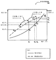
図1を参照すると、半導体チップに対する電力性能状態遷移100の一実施形態が示されている。2本の曲線が、電力対電圧と周波数対電圧との間の非線形(例えば、三次または二次)関係を示す図に示されている。5つの離散電力性能状態(P状態)が、P0〜P4として図に示されている。図を簡略化するため、少数の離散P状態を示す。5つの離散P状態のみを示しているが、他の数の離散P状態もサポートされ得る。 Referring to FIG. 1, one embodiment of a power performance state transition 100 for a semiconductor chip is shown. Two curves are shown in a diagram illustrating a non-linear (eg, third or second order) relationship between power versus voltage and frequency versus voltage. Five discrete power performance states (P states) are shown in the figure as P0-P4. To simplify the figure, a small number of discrete P states are shown. Although only five discrete P states are shown, other numbers of discrete P states may be supported.
図に示すように、P状態P4は、サポートされる全離散状態のうちの最低性能の離散状態に対応し得、最低の動作周波数を含む。さらに、P状態P4は、サポートされる全離散状態のうちの最低電力消費の離散状態に対応し得、最低の動作電圧を含む。他方、P状態P0は、サポートされる全離散状態のうちの最高性能の離散状態に対応し得、最高の動作周波数を含む。さらに、P状態P0は、サポートされる全離散状態のうちの最高電力消費の離散状態に対応し得、最高の動作電圧を含む。通常、P状態P0およびP4によって表される終点離散状態は、予測可能な性能の範囲を定義する。従って、非線形の周波数対電圧曲線に沿って、複数のP状態または動作点をサポートするようにプロセッサを構成すると、プロセッサなどの半導体チップに対して、安定した、電力の最適利用および性能の供給を提供し得る。P状態の管理は、元々はIntel Corp.、Microsoft Corp.、および株式会社東芝によって開発された、電力制御インタフェース(ACPI)規格などの業界標準に準拠し得る。 As shown in FIG, P state P 4 includes a supported minimum can correspond to the discrete state of performance, the lowest operating frequency of the total discrete states. Furthermore, P state P 4 includes can correspond to discrete states of the lowest power consumption of all the discrete states that are supported, the minimum operating voltage. On the other hand, the P state P 0 may correspond to the highest performing discrete state of all supported discrete states and includes the highest operating frequency. Further, the P state P 0 may correspond to the highest power consuming discrete state of all supported discrete states and includes the highest operating voltage. Typically, the endpoint discrete states represented by P states P 0 and P 4 define a predictable range of performance. Therefore, configuring a processor to support multiple P states or operating points along a non-linear frequency vs. voltage curve provides a stable, optimal utilization of power and performance for semiconductor chips such as processors. Can be provided. Management of the P state was originally performed by Intel Corp. , Microsoft Corp. And can be compliant with industry standards such as the Power Control Interface (ACPI) standard developed by Toshiba Corporation.
図に示すように、電力目標1(所望の電力消費レベル)が、チップに対して選択され得る。一実施形態では、選択した電力目標1が、そのチップの熱設計電力(TDP)に対応し得る。熱設計電力(TDP)は、熱設計点(thermal design point)とも呼ばれ得、コンピュータ内の冷却システムが散逸することができる最大電力量を表す。ラップトッププロセッサ用の冷却システムは、20ワットTDPに合わせて設計され得る。従って、その冷却システムは、プロセッサ内でトランジスタに対する最高接合部温度を超えることなく、20ワットを散逸することができるということが決定されている。TDP値は、チップを製造する半導体メーカーによって異なり得る。例えば、あるメーカーは、TDP値を、所与の最悪の場合の温度条件下で、既定の電圧レベルで測定した電力値として定義し得る。別のメーカーは、チップが通常のアプリケーション対高電力のウィルスアプリケーションを実行するので、TDP値を、所与の間隔に渡って測定した最大電力値として定義し得る。別の測定定義も可能であり検討される。 As shown, power target 1 (desired power consumption level) may be selected for the chip. In one embodiment, the selected power target 1 may correspond to the thermal design power (TDP) of the chip. Thermal design power (TDP) may also be referred to as a thermal design point and represents the maximum amount of power that the cooling system in the computer can dissipate. A cooling system for a laptop processor can be designed for 20 Watt TDP. Accordingly, it has been determined that the cooling system can dissipate 20 watts without exceeding the maximum junction temperature for the transistor in the processor. The TDP value may vary depending on the semiconductor manufacturer that manufactures the chip. For example, a manufacturer may define a TDP value as a power value measured at a predetermined voltage level under a given worst case temperature condition. Another manufacturer may define the TDP value as the maximum power value measured over a given interval because the chip runs a normal application versus a high power virus application. Other measurement definitions are possible and will be considered.
一実施形態では、ダイ102のプレシリコン(pre−silicon)モデル上で実行される電力モデルが、電力測定を実行し得る。設計段階の後半で、電力測定は、テスト段階およびデバッグ段階中に、実際の製造されたシリコンダイ上で実行され得る。一実施形態では、チップに対するピーク電力値が、コア上で高電力アプリケーションを実行するチップの機能的な不具合によって定義され得る。TDP値は、通常、ピーク電力値よりも低い。TDP値は、ビニング(binning)目的のため、チップの動作電圧および動作周波数を設定するために使用され得る。 In one embodiment, a power model run on a pre-silicon model of die 102 may perform power measurements. Later in the design phase, power measurements can be performed on the actual manufactured silicon die during the test and debug phases. In one embodiment, the peak power value for the chip may be defined by the functional failure of the chip running a high power application on the core. The TDP value is usually lower than the peak power value. The TDP value can be used to set the operating voltage and operating frequency of the chip for binning purposes.
図1の値電力目標1は、割り当てられたTDP値を表し得る。図1に示すように、電力目標1は、電力対電圧の非線形曲線上のデータ点Aに対応する。データ点Aは、動作電圧V2に対応する。動作電圧V2に関して、非線形の周波数対電圧曲線上のデータ点Aを突き出ると、データ点A´が提供される。データ点A´は、動作周波数F2に対応する。動作電圧V2と動作周波数F2の組合わせによって表される動作点は、チップに対して、電力の最適利用および性能の供給を提供し得る。 The value power target 1 of FIG. 1 may represent the assigned TDP value. As shown in FIG. 1, power target 1 corresponds to data point A on a non-linear curve of power versus voltage. Data points A corresponds to the operating voltage V 2. For the operating voltage V 2 , protruding a data point A on a non-linear frequency versus voltage curve provides a data point A ′. Data points A'corresponds to the operating frequency F 2. The operating point represented by the combination of operating voltage V 2 and operating frequency F 2 can provide the chip with optimal utilization of power and performance.
前述し、図に示すように、電力目標1に対する動作点は、データ点A´によって識別される。しかし、この動作点は、電力対周波数曲線上の離散P状態によって表されない。データ点A´は、P状態P1とP2との間に位置する。電力消費を削減するため、P状態P2は、対応するチップに対する最初の動作点として選択され得る。動作電圧V1と動作周波数F1の対応する組合わせは、結果として選択された動作点であり得る。この動作点は、値電力目標1より低い電力消費値に対応する。値電力P2は、P状態P2に対応する動作点の低い電力消費値を示す。 As described above and shown in the figure, the operating point for power target 1 is identified by data point A ′. However, this operating point is not represented by a discrete P state on the power versus frequency curve. Data point A ′ is located between P states P 1 and P 2 . To reduce power consumption, P state P 2 can be selected as the first operating point for the corresponding chip. The corresponding combination of operating voltage V 1 and operating frequency F 1 may result in the selected operating point. This operating point corresponds to a power consumption value lower than the value power target 1 . The value power P 2 indicates a low power consumption value at the operating point corresponding to the P state P 2 .
プロセッサなどのチップは、最初に割り当てられたP状態を利用して、(i)作業負荷が著しく変化して、報告された活動レベルにおいて著しい変化を引き起こすか、または(ii)電力モニタリングソフトウェアもしくはファームウェアによって調整されているような、最初のTDP値が変化して、図に示す電力目標値を変更するかのいずれかまで、作業負荷の処理を継続し得る。例えば、プロセッサが、やがて所与の時点で半分になる作業負荷に対する命令を実行している場合、結果として生じる全ての引き出された電流および熱エネルギーは著しく削減されるであろう。一実施形態では、当プロセッサ内に配置され得る、電力マネージャは、この状態を検出し得、それに応じて、より高い電力性能動作点に対応する異なるP状態を選択し得る。例えば、電力マネージャは、現在のP状態P2をより高い性能のP状態P1に増大つまりブーストすることを決定し得る。議論を進めるために、より高い性能のP状態は、より小さい数字をもち得る。例えば、P0は、P1より高い電力性能状態を表し得る。しかし、指定は、P0が、P1より低い電力性能状態を表すために使用されるように、逆にできる。指定のために選択されたアプローチは、単に好みの問題であり得る。 A chip, such as a processor, uses the initially assigned P state to either (i) significantly change the workload, causing a significant change in the reported activity level, or (ii) power monitoring software or firmware The workload processing can continue until either the initial TDP value, as adjusted by, changes and the power target value shown in the figure is changed. For example, if the processor is executing instructions for a workload that will eventually be halved at a given time, all the resulting drawn current and thermal energy will be significantly reduced. In one embodiment, a power manager, which may be located in the processor, may detect this state and accordingly select a different P state corresponding to a higher power performance operating point. For example, the power manager may decide to increase That boosts the current P state P 2 higher performance P state P 1. For further discussion, a higher performance P-state may have a smaller number. For example, P 0 may represent a higher power performance state than P 1 . However, the designation can be reversed so that P 0 is used to represent a lower power performance state than P 1 . The approach chosen for the designation can simply be a matter of preference.
P状態の「スロットル」は、現在選択されているP状態を1つ(または複数)のP状態だけ、低い電力消費のP状態に下げることを含む。P状態の「ブースト」は、現在選択されているP状態を1つ(または複数)のP状態だけ、高い性能のP状態に高めることを含む。P状態P2のスロットル調整は、現在選択されているP状態P2をより低い電力性能状態P3へ遷移することを含む。一例としてのP状態P2など、所与のP状態のブーストおよびスロットル調整の単純な図を図1に示す。いくつかの実施形態では、各ブースト操作および各スロットル操作は、論理回路がこの追加された複雑さをサポートする場合、現在選択されているP状態を2つ以上のP状態だけ、遷移させ得る。P状態遷移は、プロセッサ内の論理回路によって制御され得、従って、自己完結システムである。しかし、プロセッサまたはプロセッサの外部に配置されたラックコントローラ上で実行する電力管理ソフトウェアは、プロセッサに対するTDP値を変更し得、それは、図における電力目標値を変える。 P-state “throttle” includes lowering the currently selected P-state by one (or more) P-states to a low-power-consumption P-state. P-boost “boost” involves increasing the currently selected P-state by one (or more) P-states to a high-performance P-state. Throttling the P state P 2 includes transitioning the P state P 2 being currently selected to a lower power performance state P 3. A simple diagram of boost and throttle adjustment for a given P state, such as P state P 2 as an example, is shown in FIG. In some embodiments, each boost operation and each throttle operation may transition the currently selected P state by more than one P state if the logic circuit supports this added complexity. P state transitions can be controlled by logic circuits in the processor and are therefore self-contained systems. However, power management software running on the processor or a rack controller located outside the processor can change the TDP value for the processor, which changes the power target value in the figure.
図1においてP状態P2によって示される動作点は、電力目標1値よりも少ない電力を消費するが、P2によって示される動作点は、性能もより低い。測定された活動レベルにおいて著しい変化が生じるまで、より低い性能のP状態を維持するよりもむしろ、プロセッサは、現在の作業負荷に対して平均的な「仮想」動作点を達成するために、2つの離散P状態間でトグルで切り換え得る。例えば、電力マネージャは、P状態P1へブーストする前に、同一の作業負荷に対してP状態P2を利用する時間を決定し得る。同様に、電力マネージャは、P状態P2へスロットルする前に、同一の作業負荷に対してP状態P1を利用する時間を決定し得る。このプロセスは、作業負荷が著しく変化するまで何度も起こり得る。動作電圧および周波数に加えて、特定のP状態で費やした時間の平均は、図1においてデータ点A´によって表される「仮想」動作点をプロセッサが利用していた結果をもち得る。かかる方法は、任意の電力制限設定を有する柔軟な電力管理が、任意の作業負荷に対して、安定した仮想動作点(または仮想P状態)を、既存の離散P状態上に構築することにより、達成できるようにする。 The operating point indicated by P state P 2 in FIG. 1 consumes less power than the power target 1 value, but the operating point indicated by P 2 also has lower performance. Rather than maintaining a lower performance P-state until a significant change in the measured activity level occurs, the processor must achieve 2 to achieve an average “virtual” operating point for the current workload. It can be toggled between two discrete P states. For example, the power manager before the boost to the P state P 1, may determine the time to use the P state P 2 for the same workload. Similarly, the power manager before the throttle to the P state P 2, may determine the time to use the P state P 1 for the same workload. This process can occur many times until the workload changes significantly. In addition to operating voltage and frequency, the average time spent in a particular P state can have the result of the processor utilizing the “virtual” operating point represented by data point A ′ in FIG. Such a method allows flexible power management with arbitrary power limit settings to build a stable virtual operating point (or virtual P state) on an existing discrete P state for any workload, Be able to achieve.
ここで図2を参照すると、コア電力管理システム200の一実施形態が示されている。長期間にわたる動作電圧210および測定された活動レベル220に対する変化が示されている。さらに、電力目標235および平均電力対電力目標比率230が長期間にわたって示されている。図2に示すように、活動レベルが著しい変化を経験する場合および活動レベルが一定の場合の両方で、P状態遷移がある。図では、P状態遷移は動作電圧210における変化と関連がある。いくつかのP状態値が、図でラベルを付けられている。例えば、一定の活動レベル220で、P状態P1が、図に示すように低い動作電圧を有する、P状態P2へ遷移する。測定された活動レベルが一定の場合のP状態値間でのトグル切替えは、P状態ディザリングと呼ばれ得る。P状態ディザリングは、TDP値などの、チップ上で消費される平均電力と電力目標との間で1(unity)に近い比率を維持するために使用され得る。1に近いかかる比率を維持することにより、チップは、所望の量の電力(例えば、対応する冷却システムによって散逸される電力量)を消費しながら、性能を最大限にしようとし得る。
Referring now to FIG. 2, one embodiment of a core power management system 200 is shown. Changes to operating voltage 210 and measured
ここで図3を参照すると、相対的に安定した仮想動作点を作成するために、複数の離散動作点を管理するための方法300の一実施形態が示されている。議論を進めるために、この実施形態および後述する方法の後続の実施形態におけるステップは、連続した順序で示されている。しかし、いくつかのステップは、示された順序とは異なる順序で起こり得、いくつかのステップは同時に実行され得、いくつかのステップは他のステップと組み合わされ得、またいくつかのステップは別の実施形態では欠けている可能性がある。 Referring now to FIG. 3, one embodiment of a method 300 for managing a plurality of discrete operating points to create a relatively stable virtual operating point is shown. For the purposes of discussion, the steps in this embodiment and subsequent embodiments of the methods described below are shown in a sequential order. However, some steps may occur in a different order than the order shown, some steps may be performed simultaneously, some steps may be combined with other steps, and some steps may be separate This embodiment may be lacking.
ブロック302では、チップのダイ(die)に対する電力使用目標が初期化される。前述した方法を含めて、電力使用目標を選択するための様々な方法のいずれかが使用され得る。ブロック304では、そのダイに対する初期の離散電力性能状態(P状態)が所与の作業負荷において決定される。ファームウェアなどのソフトウェアおよび/またはハードウェアは、P状態を決定し得る。図に示されるようなプロセスが、P状態を決定するために使用され得る。そのダイに対する平均電力消費が、次いでブロック306で測定される。かかる測定の詳細な説明が後で提供される。ブロック308で、測定された平均電力消費が、電力目標と比較されて、差分が決定される。一実施形態では、この差分は他の決定された差分と累算され得る。例えば、累算差分値は保持され得る。別のP状態への遷移は、目標電力と測定された電力との間の差分の検出に応じて開始され得るが、かかるアプローチは、P状態間の非生産的な遷移を引き起こし得る。それ故、一実施形態では、かかる不要な遷移を防ぐために、様々な技術が利用される。一実施形態では、累算差分がP状態遷移を引き起こすのに十分な場合を判断するために、所与の変化量(delta)が使用される。例えば、測定された平均電力が目標電力を所与の変化量以上に超えると、高いP状態への遷移が開始され得るか、または許可され得る。同様に、測定された平均電力が目標電力を少なくとも所与の変化量だけ下回ると、低いP状態への遷移が開始され得るか、または許可され得る。前述した変化量は、必要に応じて、超えるかまたは単に満足する必要がある値として利用できることに留意されたい。いくつかの場合には、高いか、または低い状態への遷移の両方に対する所与の変化量は、(絶対値に関して)同じであり得る。他の実施形態では、高い状態への遷移に対して、低い状態への遷移とは異なる変化量値が使用できる。かかる全ての実施形態が検討される。さらに、変化量値は、様々な実施形態において、プログラム可能であり得るか、またはそうではない。前述に加えて、P状態遷移が起こり得るか否かを判断するために、さらなる条件が利用され得る。例えば、いくつかの実施形態では、遷移が許可される前に、P状態における最低限の滞在が必要とされ得る。さらに、かかる最低限の滞在に関する考察が、図5についての議論で提供される。ブロック310では、累算差分が所与の変化量に達すると、別のP状態への遷移が起こり得る。例えば、電力マネージャは、長期間に渡る前述の比較に対応する符号付き累算差分が所与の閾値を下回る場合、現在のP状態よりも低い電力性能状態(P状態)を選択し得る。より低いP状態は、通常、電力目標よりも低い電力消費値に相当し得る。同様に、電力マネージャは、長期間に渡る前述の比較に対応する符号付き累算差分が所与の変化量を上回る場合、現在のP状態よりもより高いP状態を選択し得る。
At block 302, a power usage target for the die of the chip is initialized. Any of a variety of methods for selecting a power usage target may be used, including the methods described above. At
再度、図2を参照すると、活動レベル220は作業負荷を追跡し得る。図2の実施形態に示すように、平均電力の電力目標に対する比率が1から変動するときに、P状態遷移が起こる。様々な実施形態では、P状態遷移がいつ起こるかを判断するために、所与の閾値分散が使用され得る。あるいは、符号付き累算差分が、比率よりむしろ、測定された平均電力と電力目標との間で見つかり得る。さらなる詳細を提供する前に、作業負荷を追跡するために活動レベルを測定する一実施形態について説明する。
Referring again to FIG. 2,
図4を参照すると、コア電力管理400の一実施形態が示されている。ここで、コア102は、任意の集積回路(IC)であり得る。一実施形態では、コア102は、プロセッサコアであり得る。プロセッサコアは、オンダイ(on −die) 命令およびデータキャッシュをもち得る。プロセッサコアは、単一のパイプラインまたは複数のパイプラインを備えたスーパースカラープロセッサであり得る。別の実施形態では、コア102は特定用途向けIC(ASIC)であり得る。コア102を実装するために、任意のトランジスタファミリーが使用され得る。例には、金属酸化膜半導体電界効果トランジスタ(MOSFET)およびバイポーラ接合トランジスタ(BJT)を含む。 Referring to FIG. 4, one embodiment of core power management 400 is shown. Here, the core 102 may be any integrated circuit (IC). In one embodiment, the core 102 may be a processor core. The processor core may have on-die instructions and a data cache. The processor core may be a superscalar processor with a single pipeline or multiple pipelines. In another embodiment, core 102 may be an application specific integrated circuit (ASIC). Any transistor family can be used to implement the core 102. Examples include metal oxide semiconductor field effect transistors (MOSFETs) and bipolar junction transistors (BJTs).
機能ブロック110は、論理関数を実行するように構成されたトランジスタ、データ記憶、またはその他を含み得る。電力管理目的のため、機能ブロック110は、ユニット132a〜132dに分割され得る。本明細書では、後ろに英字の付いた参照番号で参照される要素は、まとめて番号だけで参照され得る。例えば、ユニット132a〜132dは、まとめてユニット132と呼ばれ得る。一実施形態では、ユニット132は、リオーダ(reorder)バッファ、メモリ管理ユニット、実行ユニットなどの、プロセッサの機能コンポーネントに相当しない可能性がある。むしろ、ユニット132は、電力管理目的用にサンプリングする信号の種類に基づいて選択され得る。例えば、一実施形態では、サンプリングするために選択された信号は、ローカルクロック分配ブロックにルーティングされるクロックイネーブル信号を含む。
特定のクロックサイクル中にどの信号をサンプリングするかの選択は、その選択をユニット132内のスイッチングノード容量とどのようにうまく関連付けるかに対応し得る。クロックイネーブル信号など、サンプリングするために選択された信号は、フロアプラン内の機能ブロックと重複し得る。したがって、例えば、ユニット132aおよび132bを分離する区分は、フロアプラン内の区分に対応しない可能性がある。ユニット132は、電力を消費するユニットであり、この電力はリアルタイムで測定される。現在の作業負荷に関連付けられたダイの活動レベルは、選択されたサンプリングする信号に関連付けられた値または重みに対応し得る。
The selection of which signal to sample during a particular clock cycle may correspond to how well that selection is associated with the switching node capacity in unit 132. Signals selected for sampling, such as clock enable signals, may overlap with functional blocks in the floor plan. Thus, for example, the
一実施形態では、電力モニター130が、所与のサンプリングされた信号全ての論理値など、ユニット132からデータを収集するために使用され得る。一実施形態では、サンプリングされた信号の値が、連続的にスキャンアウトされ得る。したがって、選択された信号が、ユニット112の各々から単一のクロックサイクル内でサンプリングされ、次のサンプリングが実行される前に、連続してスキャンアウトされ得る。データの収集後、電力モニター130は、電力消費推定値を計算し得る。1つのモニター制御132が、各ユニット132に対応し得る。代替実施形態では、モニター制御132は、2つ以上のユニット112に対してデータを収集し、それらのユニット112に対する総電力消費推定値を計算し得る。さらに別の実施形態では、1つのモニター制御132(すなわち、制御132a)が、1つまたは複数のモニター制御132(すなわち、制御132b〜132d)からデータを収集するために、1つまたは複数の他のモニター制御132(すなわち、制御132b〜132d)との信号インタフェースを有し得る。次いで、1つまたは複数のモニター制御132に対する電力消費推定値が計算され得る。
In one embodiment,
信号サンプル120およびデータアウト122は、電力管理目的用に使用される制御およびデータ信号であり得る。電力モニター110と機能ブロック130との間のインタフェース信号は、任意の必要な数の信号および通信プロトコルを含み得る。一実施形態では、制御信号サンプル120は、100クロックサイクル毎など、選択した繰返し間隔中に、単一のクロックサイクルに対してのみ行使され得る。一実施形態では、制御信号サンプル120が行使された後、所与の数のクロックサイクルで、データ信号データアウト122が、各クロックサイクルの異なるサンプリングされた信号に対して、論理値の提供を開始し得る。言い換えれば、データ信号データアウト122は、特定のサイクルでサンプリングされた信号の論理値を含む一連の値を完全にスキャンするために使用され得る。また、他の実施形態では、モニター制御132とユニット112の各対の間に、単一対の信号がない可能性がある。代替実施形態では、モニター制御132がユニット112をポーリング(poll)するため、ユニット112が出力データを伝達する準備ができていることをモニター制御132に対して肯定応答するために、追加の信号が含まれ得る。
Signal sample 120 and data out 122 may be control and data signals used for power management purposes. Interface signals between the
所与の時間間隔中に複数のサンプルが取得され得る。活動レベルを計算する前に使用する断続的なクロックサイクル数の決定は、サンプリングされたデータの所望の精度および信頼性によって決まり得る。スプレッドシートまたはルックアップテーブルが、アプリケーションの実際の電力消費およびサンプリングからの推定電力消費の両方の統計分析および測定の両方を用いて、生成され得る。統計分析をさらに展開するために、信頼性レベルおよび誤り率が選択され得る。リアルタイム電力推定方法の一例に、2008年4月11日に出願された「Sampling Chip Activity for Real Time Power Estimation」という名称の出願整理番号第12/101,598号があり、その内容全体が参照により本明細書に組み込まれる。 Multiple samples can be acquired during a given time interval. The determination of the number of intermittent clock cycles to use before calculating the activity level can depend on the desired accuracy and reliability of the sampled data. A spreadsheet or lookup table can be generated using both statistical analysis and measurement of both the actual power consumption of the application and the estimated power consumption from sampling. To further develop the statistical analysis, a confidence level and error rate can be selected. An example of a real-time power estimation method is an application serial number 12 / 101,598 entitled “Sampling Chip Activity for Real Time Power Estimation” filed on April 11, 2008, the entire contents of which are incorporated by reference. Incorporated herein.
電力モニター130が、機能ブロック110から繰返し間隔にわたって受信したデータから電力消費推定値を計算するとき、電力モニター130は、現在実行しているアプリケーションの電力プロファイルを決定している。この決定は、電力マネージャ140に伝達される。電力マネージャ140は、アプリケーションが閾値制限を上(下)回っている場合に電力を削減(または増加)するために、機能ブロック110の動作点を変更し得る。例えば、電力マネージャ140は、現在のP状態をブーストまたはスロットルさせて、別の所与のP状態へ遷移させ得る。
When the
一実施形態では、上記した特定の期間中、電力マネージャ140は、電力モニター130によって提供された電力プロファイルと電力目標との間で符号付きの継続的な累算差分を計算し得る。この場合も、電力目標は熱設計点(TDP)であり得る。累算差分は、各所与の時間間隔の終わりに、AccTdpDelta=AccTdpDelta+(TDP−RcvdPwr)として計算され得る。ここで、変数AccTdpDeltaは、符号付きの継続的な累算差分である。変数TDPは、割り当てられた熱設計電力、または相当数の熱クレジット(thermal credit)である。変数RcvdPwrは、電力モニター130から受信した電力消費推定値である。この値は、機能ブロック110内のサンプリングされた信号を測定することにより、ダイの活動レベルを追跡し得る。
In one embodiment, during the particular time period described above,
変数RcvdPwrによって表される測定された活動レベルがTDPより高ければ、累算値AccTdpDeltaは、負の値の方へ押される。累算値が負の所与の閾値に達すると、電力マネージャは、現在のP状態をスロットル調整することを決定し得る。再度、図1を参照すると、現在のP状態をスロットル調整する一例は、P状態P1からP状態P2へ遷移することであろう。かかる状況は、コア内で活動レベルが高い場合に起こり得る。活動レベルが高い値のままである場合、電力マネージャが徐々に現在のP状態をスロットル調整し続け得る。 If the measured activity level represented by the variable RcvdPwr is higher than TDP, the accumulated value AccTdpDelta is pushed towards a negative value. When the accumulated value reaches a given negative threshold, the power manager may decide to throttle the current P state. Referring again to FIG. 1, one example of throttle adjusting the current P state would be to transition from P state P 1 to P state P 2 . Such a situation can occur when the activity level is high in the core. If the activity level remains high, the power manager may gradually continue to throttle the current P state.
測定された活動レベルがTDPより低ければ、累算値AccTdpDeltaは、正の値の方へ押される。累算値が正の所与の閾値に達すると、電力マネージャ140は、現在のP状態をブーストすることを決定し得る。再度、図1を参照すると、現在のP状態をブーストする一例は、P状態P2からP状態P1へ遷移することであろう。かかる状況は、コア内で活動レベルが低い場合に起こり得る。活動レベルが低い値のままである場合、電力マネージャが徐々に現在のP状態をブーストし続け得る。
If the measured activity level is below TDP, the accumulated value AccTdpDelta is pushed towards a positive value. When the accumulated value reaches a given positive threshold,
電力マネージャ140は、電力モニター130から送信された情報が、温度情報ではなく、コア102内の実際の活動レベルおよび電力消費に相当する場合、コア102内の潜在的な熱的問題に対してより素早い対応を提供することができ得る。半導体チップダイのダイ全体に配置されているアナログまたはデジタルの熱センサーが、長い期間をかけて温度波形を決定し得る。熱センサーは、増大した計算活動に起因して、特定の領域でいつダイが熱くなるかに関する時の情報を提供する。しかし、これらのセンサーは、熱に関する各変化が、コア102内での計算に関連した電力消費の増加によるか、または周囲温度の上昇などの外部の環境要因によって駆動されたかにかかわらず、応答する。例えば、データセンター内のラックシステム内の周囲のサーバーが、周囲温度の上昇を引き起こし得る。特定のコア内のスイッチング容量は、時間間隔にわたって変化しないかもしれないが、センサーは、周囲温度の上昇に起因した高い熱エネルギー消費を報告し得る。さらに、計算に関連した電力消費の増加と温度上昇との間に時間遅延がある。それ故、平均電力消費と電力目標との間で1の比率を維持しようとしながら、コア内の活動レベルとスイッチング容量に関連した測定値を温度の測定値と対比して、より良い結果が提供され得る。
The
ここで、図5を参照すると、安定した仮想動作点を作成するために、複数の離散動作点を管理するための方法500の別の実施形態が示されている。議論を進めるために、この実施形態および後述する方法の後続の実施形態におけるステップは、連続した順序で示されている。しかし、いくつかのステップは、示された順序とは異なる順序で起こり得、いくつかのステップは同時に実行され得、いくつかのステップは他のステップと組み合わされ得、またいくつかのステップは別の実施形態では欠けている可能性がある。 Referring now to FIG. 5, another embodiment of a method 500 for managing a plurality of discrete operating points to create a stable virtual operating point is shown. For the purposes of discussion, the steps in this embodiment and subsequent embodiments of the methods described below are shown in a sequential order. However, some steps may occur in a different order than the order shown, some steps may be performed simultaneously, some steps may be combined with other steps, and some steps may be separate This embodiment may be lacking.
ブロック502では、半導体チップが1つまたは複数のソフトウェアアプリケーションの命令を実行する。所与のサンプリング間隔の終わりに達すると(条件ブロック504)、ブロック506で、電力消費推定値が決定され、電力マネージャに伝達される。電力消費推定値は、前述したように、機能ブロック内で選択した信号をサンプリングすること、および対応する重みをサンプリングされた信号に関連付けることにより見つかり得る。決定した電力推定値のカウントに対応するカウンタの値が増加され得る。ブロック508では、電力マネージャが、TDPなどの所与の電力目標と、受信した電力消費値との間で符号付き累算差分を計算し得る。その計算は、前述したように、AccTdpDelta=AccTdpDelta+(TDP−RcvdPwr)であり、式中、変数RcvdPwrは、受信した電力消費値を表す。
At block 502, the semiconductor chip executes instructions for one or more software applications. When the end of a given sampling interval is reached (condition block 504), at
P状態遷移が起こる場合、符号付き累算差分AccTdpDeltaは、別のサンプル間隔が起こる時まで、所与の閾値をまだ超えていることに留意されたい。例えば、P状態P2からP状態P1へのブーストは、AccTdpDeltaが正のブースト閾値よりも大きい値に起因して起こり得る。P状態遷移の後、次の時間間隔で、符号付き累算差分AccTdpDeltaは、正のブースト閾値よりもより大きい可能性がある。測定された電力消費値がTDP値を超えるのに十分な時間がなかった可能性がある。したがって、現在のP状態が所与の時間に最良の電力性能動作点を提供すると判断される前に、現在のP状態を素早くブーストし続けることは可能である。 Note that when a P state transition occurs, the signed accumulated difference AccTdpDelta still exceeds the given threshold until another sample interval occurs. For example, the boost from the P state P 2 to P state P 1 is, AccTdpDelta can occur due to a larger value than the positive boost threshold. At the next time interval after the P state transition, the signed accumulated difference AccTdpDelta may be greater than the positive boost threshold. It may be that there was not enough time for the measured power consumption value to exceed the TDP value. Thus, it is possible to continue to quickly boost the current P state before it is determined that the current P state provides the best power performance operating point at a given time.
前述のとおり、迅速なP状態遷移を防ぐため、次のP状態遷移は、現在のP状態遷移後の所与の間、起こるのが許可されない可能性がある。所与の期間は、最低限の滞在と呼ばれ得る。一実施形態では、現在のP状態遷移の後に許容可能な期間が経過しているかを判断するために、カウンタが使用され得る。そのカウンタ値は、所与の閾値と比較され得る。あるいは、カウンタが、所与の閾値と共にロードされ、ゼロの値まで減少され得る。この許容可能な期間が経過すると、別のP状態遷移が起こり得る。 As described above, to prevent rapid P state transitions, the next P state transition may not be allowed to occur for a given time after the current P state transition. A given period can be referred to as a minimum stay. In one embodiment, a counter may be used to determine if an acceptable period has elapsed after the current P state transition. The counter value can be compared to a given threshold. Alternatively, a counter can be loaded with a given threshold and decremented to a value of zero. When this acceptable period elapses, another P state transition can occur.
さらに、累算差分AccTdpDeltaに関して熟成値(value aging)が使用され得る。熟成値は、チップダイの加熱を防ぐのに役立ち得る。熟成された累算差分は、長い間、高い電力P状態間での遷移またはディザリング(dithering)のままであり得る。累算差分AccTdpDeltaは、P状態がスロットル調整される場合、累算し続け得る。しばらくすると、累算差分は、ブースト用に利用可能な実際の熱エネルギーの上方空間をもはや表していない可能性がある。したがって、時々、累算差分AccTdpDeltaは、所与の期間の終わりに、リセット値に設定され得る。リセット値は、累算差分AccTdpDeltaの現在の値の何分の1からゼロまで異なり得る。構成レジスタに格納された値が、リセット値を決定するために使用され得る。例えば、第1の格納された値は、累算差分AccTdpDeltaに等しいリセット値に相当し得る。第2の格納された値は、シフトされた(例えば、2による除算、4による除算など)累算差分AccTdpDeltaに等しいリセット値に相当し得る。第3の格納された値は、ゼロに等しいリセット値に相当し得る。 Further, a value aging can be used for the accumulated difference AccTdpDelta. The aging value can help prevent the die die from heating. The mature accumulated difference can remain a transition or dithering between high power P states for a long time. The accumulated difference AccTdpDelta can continue to accumulate if the P state is throttled. After a while, the accumulated difference may no longer represent the actual space above the actual thermal energy available for boost. Thus, from time to time, the accumulated difference AccTdpDelta can be set to a reset value at the end of a given period. The reset value can vary from a fraction of the current value of the accumulated difference AccTdpDelta to zero. The value stored in the configuration register can be used to determine the reset value. For example, the first stored value may correspond to a reset value equal to the accumulated difference AccTdpDelta. The second stored value may correspond to a reset value equal to the accumulated difference AccTdpDelta, which is shifted (eg, division by 2, division by 4, etc.). The third stored value may correspond to a reset value equal to zero.
一例では減少され得るカウンタが、前述した所与の期間を設定し得る。そのカウンタは、値Nをロードし得、それは、構成レジスタに格納される。累算差分AccTdpDeltaが各サンプルの終わりに更新される、N個のサンプルが生じた後、または時間間隔の後、累算差分AccTdpDeltaがリセットされ得る。値Nと共にロードされたカウンタは、累算差分AccTdpDeltaの符号が変わるたびにリセットされ得る。 In one example, a counter that can be decremented may set the given time period described above. The counter can load the value N, which is stored in the configuration register. The accumulated difference AccTdpDelta is updated at the end of each sample, after N samples have occurred, or after a time interval, the accumulated difference AccTdpDelta can be reset. The counter loaded with the value N may be reset whenever the sign of the accumulated difference AccTdpDelta changes.
再度、図5の方法500を参照すると、P状態の最低限の滞在期間に達していない場合(条件ブロック510)、N個のサンプルが生じているか否かに関して、チェックが実行される。各サンプル間隔の終わりに、ダイに対して新しい電力消費値が決定され、新しい値が、累算差分AccTdpDeltaに対して計算される。N個のサンプルのカウントが生じている場合(条件ブロック516)には、ブロック518で、累算差分AccTdpDeltaが、前述のように、所与のリセット値に設定される。
Referring again to the method 500 of FIG. 5, if the minimum stay period of the P state has not been reached (condition block 510), a check is performed as to whether N samples have occurred. At the end of each sample interval, a new power consumption value is determined for the die and a new value is calculated for the accumulated difference AccTdpDelta. If a count of N samples has occurred (condition block 516), at
P状態の最低限の滞在期間に達した場合(条件ブロック510)には、ブーストおよびスロットル閾値に関するチェックが実行される。符号付き累算差分AccTdpDeltaが閾値を超えているか否かを判断するために比較が実行され得る。例えば、累算差分AccTdpDeltaは、正のブースト閾値よりも大きい可能性がある。あるいは、累算差分AccTdpDeltaは、負のスロットル閾値よりも小さい可能性がある。累算差分AccTdpDeltaが閾値を超えている場合(条件ブロック512)には、ブロック514で、対応する次のP状態が、チップダイに対して選択される。例えば、符号付き累算差分AccTdpDeltaが正の(ブースト)閾値よりも大きい場合は、現在のP状態よりも高い電力性能のP状態への遷移が起こり得る。あるいは、符号付き累算差分AccTdpDeltaが負のスロットル閾値よりも小さい場合には、現在のP状態よりも低い電力性能のP状態への遷移が起こり得る。 If the minimum stay period for the P state has been reached (condition block 510), a check for boost and throttle thresholds is performed. A comparison may be performed to determine whether the signed accumulated difference AccTdpDelta exceeds a threshold. For example, the accumulated difference AccTdpDelta may be greater than a positive boost threshold. Alternatively, the accumulated difference AccTdpDelta may be smaller than the negative throttle threshold. If the accumulated difference AccTdpDelta exceeds the threshold (condition block 512), at block 514, the corresponding next P state is selected for the chip die. For example, if the signed accumulated difference AccTdpDelta is greater than a positive (boost) threshold, a transition to a P state with higher power performance than the current P state may occur. Alternatively, if the signed accumulated difference AccTdpDelta is less than the negative throttle threshold, a transition to a P state with lower power performance than the current P state may occur.
一実施形態では、プロセッサが複数のコアを含む場合、電力消費推定値が各コア内で計算され得る。さらに、各コアが、符号付き累算差分AccTdpDeltaを決定し得る。複数のコアのいずれかがブーストまたはスロットル閾値を超える場合、プロセッサ全体に対するP状態がそれに応じて遷移し得る。その後、方法500の制御フローが条件ブロック516に進む。
In one embodiment, if the processor includes multiple cores, a power consumption estimate may be calculated within each core. Furthermore, each core may determine a signed accumulated difference AccTdpDelta. If any of the multiple cores exceeds the boost or throttle threshold, the P state for the entire processor may transition accordingly. Thereafter, the control flow of method 500 proceeds to
前述の実施形態は、ソフトウェアを含み得ることに留意されたい。かかる実施形態では、説明したシステムおよび/または方法を表すプログラム命令および/またはデータベース(その両方とも「命令」と呼ばれ得る)は、伝達されるか、またはコンピュータ可読媒体上に格納され得る。一般的に、コンピュータアクセス可能記憶媒体は、使用中にコンピュータに命令および/またはデータを提供するために、コンピュータによってアクセス可能な任意の記憶媒体を含み得る。例えば、コンピュータアクセス可能記憶媒体には、磁気または光媒体などの記憶媒体、例えば、ディスク(固定または取外し可能)、テープ、CD−ROM、もしくはDVD−ROM、CD−R、CD−RW、DVD−R、DVD−RW、もしくはブルーレイなどを含み得る。記憶媒体には、RAM(例えば、シンクロナスダイナミックRAM(SDRAM)、ダブルデータレート(DDR、DDR2、DDR3など)SDRAM、低電力DDR(LPDDR2など)SDRAM、Rambus DRAM(RDRAM)、スタティックRAM(SRAM)など)、ROM、フラッシュメモリ、ユニバーサルシリアルバス(USB)インタフェースなどの周辺インタフェースを介してアクセス可能な不揮発性メモリ(例えば、フラッシュメモリ)などの、揮発性または不揮発性の記憶媒体をさらに含み得る。記憶媒体には、微小電気機械システム(MEMS)ならびに、ネットワークおよび/または無線リンクなどの通信媒体を介してアクセス可能な記憶媒体を含み得る。 Note that the foregoing embodiments may include software. In such embodiments, program instructions and / or databases (both of which may be referred to as “instructions”) representing the described systems and / or methods may be communicated or stored on a computer readable medium. Generally, computer-accessible storage media may include any storage media accessible by a computer to provide instructions and / or data to the computer during use. For example, the computer-accessible storage medium includes a storage medium such as magnetic or optical medium, such as a disk (fixed or removable), tape, CD-ROM, or DVD-ROM, CD-R, CD-RW, DVD- R, DVD-RW, or Blu-ray may be included. Storage media include RAM (eg, synchronous dynamic RAM (SDRAM), double data rate (DDR, DDR2, DDR3, etc.) SDRAM, low power DDR (LPDDR2 etc.) SDRAM, Rambus DRAM (RDRAM), static RAM (SRAM) Etc.), volatile or non-volatile storage media such as ROM, flash memory, non-volatile memory (eg, flash memory) accessible via a peripheral interface such as a universal serial bus (USB) interface. Storage media may include microelectromechanical systems (MEMS) and storage media accessible via communication media such as networks and / or wireless links.
さらに、命令は、Cなどのプログラム言語、またはVerilog、VHDLなどの設計言語、またはGDS IIストリーム形式(GDSII)などのデータベース形式において、ハードウェア機能の動作レベル記述またはレジスタ転送レベル(RTL)記述を含み得る。これらの命令は、次いで、システム(またはシステムの一部)を含むハードウェアを製作するために、読み取られ、使用され得る。いくつかの場合には、記述は、設計の実装を形成するために、合成ツール(例えば、コンピューティング装置上で実行するプログラムコード)によって読み取られ得る。例えば、かかるツールは、合成ライブラリ(synthesis library)からのゲートのリストを含むネットリストを生成するため、記述を合成するために使用され得る。ネットリストは通常、システムを含むハードウェアの機能も表すゲートのセットを含み得る。ネットリストは、次いで、マスクに適用される幾何学的形態を記述するデータセットを生成するために配置およびルーティングされ得る。マスクは、次いで、システムに対応する半導体回路または回路を生産する様々な半導体製造ステップで使用され得る。あるいは、コンピュータアクセス可能記憶媒体上の命令は、必要に応じて、ネットリスト(合成ライブラリの有無に関わらない)またはデータセットであり得る。さらに、命令は、CadenceR、EVER、およびMentor GraphicsRの各ベンダーからのものなど、ハードウェアベースタイプのエミュレータによるエミュレーションのために利用され得る。例えば、かかる実施形態では、命令は、設計に従って実行するため、FPGAベースのハードウェアを構成するために利用され得る。多数のかかる実施形態が可能であり、検討される。 In addition, the instructions can describe the operation level description or register transfer level (RTL) description of the hardware function in a programming language such as C, a design language such as Verilog or VHDL, or a database format such as GDS II stream format (GDSII). May be included. These instructions can then be read and used to create the hardware that contains the system (or part of the system). In some cases, the description may be read by a synthesis tool (eg, program code executing on a computing device) to form an implementation of the design. For example, such a tool can be used to synthesize a description to generate a netlist that includes a list of gates from a synthesis library. A netlist may typically include a set of gates that also represent the functions of the hardware that contains the system. The netlist can then be placed and routed to generate a data set that describes the geometric form applied to the mask. The mask can then be used in various semiconductor manufacturing steps to produce a semiconductor circuit or circuit corresponding to the system. Alternatively, the instructions on the computer-accessible storage medium may be a netlist (with or without a synthesis library) or a data set, as appropriate. Further, the instructions may be utilized for emulation by hardware based type emulators such as those from CadenceR, EVER, and Mentor GraphicsR vendors. For example, in such an embodiment, instructions may be utilized to configure FPGA-based hardware to execute according to design. Many such embodiments are possible and are contemplated.
前述の実施形態はかなり詳細に説明しているが、前述の開示を十分に理解すると、多数の変形および修正が当業者には明らかになるであろう。以下の特許請求の範囲が、かかる全ての変形および修正を包含するものと解釈されることを意図する。 Although the foregoing embodiments have been described in considerable detail, numerous variations and modifications will become apparent to those skilled in the art once the above disclosure is fully appreciated. It is intended that the following claims be construed to include all such variations and modifications.
Claims (20)
前記1つ以上の機能ブロックに接続された、前記プロセッサコア内の電力マネージャとを備え、
前記電力マネージャは、
所望の電力消費に対応する仮想P状態であって、サポートされた離散P状態ではない仮想P状態を決定し、
前記仮想P状態よりも低い低P状態及び前記仮想P状態よりも高い高P状態のそれぞれに用いられる、個々の最短滞留時間を決定し、
前記低P状態又は前記高P状態に対応する電力消費よりも前記所望の電力消費により緊密に一致する平均電力消費を経時的に生成するために、前記個々の最短滞留時間を用いて、前記低P状態及び前記高P状態を交互に選択し且つ伝達するように構成されている、
コンピューティングシステム。 One or more functional blocks in the processor core configured to generate data according to the activity level of each block, operating in one or more discrete power performance states (discrete P states) Functional blocks configured in
A power manager in the processor core connected to the one or more functional blocks;
The power manager
Determining a virtual P-state corresponding to a desired power consumption and not a supported discrete P-state;
Determining an individual shortest dwell time used for each of a low P state lower than the virtual P state and a high P state higher than the virtual P state;
In order to generate an average power consumption over time that more closely matches the desired power consumption than the power consumption corresponding to the low P state or the high P state, Configured to alternately select and communicate the P state and the high P state;
Computing system.
少なくとも現在のP状態の最短滞留時間が経過したのを判定したことに応じて、次のP状態を選択するように構成されている、請求項1に記載のコンピューティングシステム。 The power manager
The computing system of claim 1, wherein the computing system is configured to select a next P state in response to determining that at least the shortest dwell time of the current P state has elapsed.
前記データに少なくとも一部基づいて、前記1つ以上の機能ブロックのうち1つの機能ブロックに対して、所与の時間間隔中に平均電力消費を決定し、
前記平均電力消費が前記所望の電力消費を、少なくとも、ゼロよりも大きい絶対値を有する第1の変化量だけ超えているという判断に応じて、現在のP状態よりも低いP状態を選択し、
前記平均電力消費が前記所望の電力消費を、少なくとも、ゼロよりも大きい絶対値を有する第2の変化量だけ下回っているという判断に応じて、現在のP状態よりも高いP状態を選択するように構成されている、請求項1に記載のコンピューティングシステム。 The power manager
Determining an average power consumption during a given time interval for one functional block of the one or more functional blocks based at least in part on the data;
In response to determining that the average power consumption exceeds the desired power consumption by at least a first variation having an absolute value greater than zero, selecting a P state lower than the current P state;
Selecting a P state that is higher than the current P state in response to determining that the average power consumption is less than the desired power consumption by at least a second variation having an absolute value greater than zero. The computing system according to claim 1, which is configured as follows.
前記所望の電力消費と複数の機能ブロックの電力消費値との間で、符号付き累算差分を経時的に決定し、
前記符号付き累算差分が、ゼロよりも大きい絶対値を有する第1の変化量より大きいという判断に応じて、現在のP状態よりも低いP状態を選択し、
前記符号付き累算差分が、ゼロよりも大きい絶対値を有する第2の変化量より少ないという判断に応じて、現在のP状態よりも高いP状態を選択するようにさらに構成されている、
請求項3に記載のコンピューティングシステム。 The power manager
Determining a signed accumulated difference over time between the desired power consumption and the power consumption values of the plurality of functional blocks;
In response to determining that the signed accumulated difference is greater than a first variation having an absolute value greater than zero, selecting a P state lower than the current P state;
Further configured to select a P state that is higher than the current P state in response to determining that the signed accumulated difference is less than a second variation having an absolute value greater than zero;
The computing system according to claim 3 .
個々の電力性能状態(P状態)で動作する1つ以上の機能ブロックの活動レベルに応じて、データを生成することと、
所望の電力消費に対応する仮想P状態であって、サポートされた離散P状態と等しくない仮想P状態を決定することと、
前記仮想P状態よりも低い低P状態及び前記仮想P状態よりも高い高P状態のそれぞれに用いられる、個々の最短滞留時間を決定することと、
前記低P状態又は前記高P状態に対応する電力消費よりも前記所望の電力消費により緊密に一致する平均電力消費を経時的に生成するために、前記個々の最短滞留時間を用いて、前記低P状態及び前記高P状態を交互に選択し且つ伝達することと、
を含む方法。 A method performed by a computing system for managing a plurality of discrete operating points to create a stable virtual operating point, comprising:
Generating data according to the activity level of one or more functional blocks operating in an individual power performance state (P state);
Determining a virtual P-state corresponding to the desired power consumption and not equal to the supported discrete P-state;
Determining an individual shortest dwell time used for each of a low P state lower than the virtual P state and a high P state higher than the virtual P state;
In order to generate an average power consumption over time that more closely matches the desired power consumption than the power consumption corresponding to the low P state or the high P state, Alternately selecting and communicating the P state and the high P state;
Including methods.
前記平均電力消費が前記所望の電力消費を、少なくとも、ゼロよりも大きい絶対値を有する第1の変化量だけ超えているという判断に応じて、現在のP状態よりも低いP状態を選択することと、
前記平均電力消費が前記所望の電力消費を、少なくとも、ゼロよりも大きい絶対値を有する第2の変化量だけ下回っているという判断に応じて、現在のP状態よりも高いP状態を選択することとをさらに含む、請求項9に記載の方法。 Determining an average power consumption during a given time interval for one of the one or more functional blocks based at least in part on the data;
Selecting a P state lower than the current P state in response to determining that the average power consumption exceeds the desired power consumption by at least a first variation having an absolute value greater than zero. When,
Selecting a P state higher than the current P state in response to determining that the average power consumption is less than the desired power consumption by at least a second variation having an absolute value greater than zero. 10. The method of claim 9, further comprising:
前記符号付き累算差分が、ゼロよりも大きい絶対値を有する第1の変化量より大きいという判断に応じて、現在のP状態よりも低いP状態を選択することと、
前記符号付き累算差分が、ゼロよりも大きい絶対値を有する第2の変化量より少ないという判断に応じて、現在のP状態よりも高いP状態を選択することとをさらに含む、
請求項11に記載の方法。 Determining a signed accumulated difference over time between the desired power consumption and power consumption values of a plurality of functional blocks;
Selecting a P state lower than the current P state in response to determining that the signed accumulated difference is greater than a first variation having an absolute value greater than zero;
Selecting a P state higher than the current P state in response to determining that the signed accumulated difference is less than a second variation having an absolute value greater than zero;
The method of claim 11 .
前記符号付き累算差分の符号が変わったか、または前記カウントがNに達したかの検出に応じて、どちらが最初に起こったかにより、前記カウントをリセットすることをさらに含む、請求項14に記載の方法。 The time interval includes a maximum count of N functional block sample intervals;
The method of claim 14, further comprising resetting the count according to which occurred first in response to detecting whether the sign of the signed accumulated difference has changed or the count has reached N.
前記プログラム命令は、
個々の電力性能状態(P状態)で動作する1つ以上の機能ブロックの活動レベルに応じて、データを生成し、
所望の電力消費に対応する仮想P状態であって、サポートされた離散P状態と等しくない仮想P状態を決定し、
前記仮想P状態よりも低い低P状態及び前記仮想P状態よりも高い高P状態のそれぞれに用いられる、個々の最短滞留時間を決定し、
前記低P状態又は前記高P状態に対応する電力消費よりも前記所望の電力消費により緊密に一致する平均電力消費を経時的に生成するために、前記個々の最短滞留時間を用いて、前記低P状態及び前記高P状態を交互に選択し且つ伝達する、ように実行可能である、
コンピュータ可読記憶媒体。 A computer-readable storage medium storing program instructions that function to manage a plurality of discrete operating points to create a stable virtual operating point,
The program instructions are:
Generate data according to the activity level of one or more functional blocks operating in individual power performance states (P states);
Determining a virtual P-state corresponding to the desired power consumption and not equal to the supported discrete P-state;
Determining an individual shortest dwell time used for each of a low P state lower than the virtual P state and a high P state higher than the virtual P state;
In order to generate an average power consumption over time that more closely matches the desired power consumption than the power consumption corresponding to the low P state or the high P state, It is feasible to alternately select and communicate the P state and the high P state.
Computer-readable storage medium.
前記データに少なくとも一部基づいて、前記1つ以上の機能ブロックのうち1つの機能ブロックに対して、所与の時間間隔中に平均電力消費を決定し、
前記平均電力消費が前記所望の電力消費を、少なくとも、ゼロよりも大きい絶対値を有する第1の変化量だけ超えているという判断に応じて、現在のP状態よりも低いP状態を選択し、
前記平均電力消費が前記所望の電力消費を、少なくとも、ゼロよりも大きい絶対値を有する第2の変化量だけ下回っているという判断に応じて、現在のP状態よりも高いP状態を選択する、ようにさらに実行可能である、請求項18に記載のコンピュータ可読記憶媒体。 The program instructions are:
Determining an average power consumption during a given time interval for one functional block of the one or more functional blocks based at least in part on the data;
In response to determining that the average power consumption exceeds the desired power consumption by at least a first variation having an absolute value greater than zero, selecting a P state lower than the current P state;
Selecting a P state higher than the current P state in response to determining that the average power consumption is less than the desired power consumption by at least a second variation having an absolute value greater than zero; The computer-readable storage medium of claim 18, further executable.
前記所望の電力消費と複数の機能ブロックの電力消費値との間で、符号付き累算差分を経時的に決定し、
前記符号付き累算差分が、ゼロよりも大きい絶対値を有する第1の変化量より大きいという判断に応じて、現在のP状態よりも低いP状態を選択し、
前記符号付き累算差分が、ゼロよりも大きい絶対値を有する第2の変化量より少ないという判断に応じて、現在のP状態よりも高いP状態を選択する、ようにさらに実行可能である、請求項19に記載のコンピュータ可読記憶媒体。 The program instructions are:
Determining a signed accumulated difference over time between the desired power consumption and the power consumption values of the plurality of functional blocks;
In response to determining that the signed accumulated difference is greater than a first variation having an absolute value greater than zero, selecting a P state lower than the current P state;
In response to determining that the signed accumulated difference is less than a second variation having an absolute value greater than zero, further selecting a P state that is higher than the current P state is possible. The computer-readable storage medium according to claim 19.
Applications Claiming Priority (3)
| Application Number | Priority Date | Filing Date | Title |
|---|---|---|---|
| US12/819,777 US8504854B2 (en) | 2010-06-21 | 2010-06-21 | Managing multiple operating points for stable virtual frequencies |
| US12/819,777 | 2010-06-21 | ||
| PCT/US2011/041291 WO2011163261A1 (en) | 2010-06-21 | 2011-06-21 | Managing multiple operating points for stable virtual frequencies |
Publications (3)
| Publication Number | Publication Date |
|---|---|
| JP2013533548A JP2013533548A (en) | 2013-08-22 |
| JP2013533548A5 JP2013533548A5 (en) | 2014-08-07 |
| JP5676759B2 true JP5676759B2 (en) | 2015-02-25 |
Family
ID=44546037
Family Applications (1)
| Application Number | Title | Priority Date | Filing Date |
|---|---|---|---|
| JP2013516697A Active JP5676759B2 (en) | 2010-06-21 | 2011-06-21 | Management of multiple operating points for stable virtual frequency |
Country Status (6)
| Country | Link |
|---|---|
| US (1) | US8504854B2 (en) |
| EP (1) | EP2583151B1 (en) |
| JP (1) | JP5676759B2 (en) |
| KR (1) | KR101718116B1 (en) |
| CN (1) | CN102971687B (en) |
| WO (1) | WO2011163261A1 (en) |
Families Citing this family (21)
| Publication number | Priority date | Publication date | Assignee | Title |
|---|---|---|---|---|
| US8510582B2 (en) * | 2010-07-21 | 2013-08-13 | Advanced Micro Devices, Inc. | Managing current and power in a computing system |
| US8984305B2 (en) * | 2010-12-21 | 2015-03-17 | Intel Corporation | Method and apparatus to configure thermal design power in a microprocessor |
| US9442732B2 (en) * | 2012-03-19 | 2016-09-13 | Via Technologies, Inc. | Running state power saving via reduced instructions per clock operation |
| EP2725450A4 (en) * | 2012-08-30 | 2015-07-08 | Huawei Device Co Ltd | Method and device for controlling central processing unit |
| US9218044B2 (en) * | 2012-11-27 | 2015-12-22 | International Business Machines Corporation | Computing system frequency target monitor |
| US9323300B2 (en) * | 2012-11-27 | 2016-04-26 | International Business Machines Corporation | Computing system voltage control |
| JP5764150B2 (en) * | 2013-01-16 | 2015-08-12 | レノボ・シンガポール・プライベート・リミテッド | Method and computer for transition from power-on state to power-saving state |
| US9436265B2 (en) * | 2013-10-24 | 2016-09-06 | Fujitsu Limited | Information processing apparatus and load control method |
| US9436263B2 (en) * | 2014-02-21 | 2016-09-06 | Qualcomm Incorporated | Systems and methods for power optimization using throughput feedback |
| US9934831B2 (en) | 2014-04-07 | 2018-04-03 | Micron Technology, Inc. | Apparatuses and methods for storing and writing multiple parameter codes for memory operating parameters |
| JP6356502B2 (en) | 2014-06-20 | 2018-07-11 | 株式会社東芝 | Equipment operation setting device and equipment operation setting value determination program |
| EP3210420B1 (en) * | 2014-10-24 | 2018-08-15 | Telefonaktiebolaget LM Ericsson (publ) | Power management of a wireless communication device |
| US9847662B2 (en) | 2014-10-27 | 2017-12-19 | Sandisk Technologies Llc | Voltage slew rate throttling for reduction of anomalous charging current |
| US9916087B2 (en) | 2014-10-27 | 2018-03-13 | Sandisk Technologies Llc | Method and system for throttling bandwidth based on temperature |
| US9880605B2 (en) * | 2014-10-27 | 2018-01-30 | Sandisk Technologies Llc | Method and system for throttling power consumption |
| FR3054885B1 (en) | 2016-08-03 | 2018-09-07 | Stmicroelectronics (Crolles 2) Sas | METHOD FOR ESTIMATING AN OPERATING PROFILE OF AN INTEGRATED CIRCUIT OF A SYSTEM ON A CHIP, AND A SYSTEM THEREON ON A CHIP CORRESPONDING |
| FR3054949A1 (en) * | 2016-08-03 | 2018-02-09 | Stmicroelectronics (Crolles 2) Sas | METHOD FOR ADJUSTING AT LEAST ONE OPERATING POINT OF AT LEAST ONE INTEGRATED CIRCUIT OF AN ON-CHIP SYSTEM, AND CORRESPONDING CHIP SYSTEM |
| JP2020061124A (en) * | 2018-10-05 | 2020-04-16 | 富士通株式会社 | Parallel processor and arithmetic processing method |
| US11940859B2 (en) | 2018-11-16 | 2024-03-26 | Hewlett Packard Enterprise Development Lp | Adjusting power consumption limits for processors of a server |
| US11409560B2 (en) * | 2019-03-28 | 2022-08-09 | Intel Corporation | System, apparatus and method for power license control of a processor |
| US11360827B2 (en) | 2019-06-04 | 2022-06-14 | Hewlett Packard Enterprise Development Lp | Regulating core and un-core processor frequencies of computing node clusters |
Family Cites Families (60)
| Publication number | Priority date | Publication date | Assignee | Title |
|---|---|---|---|---|
| US3382460A (en) | 1967-09-11 | 1968-05-07 | Sanders Associates Inc | Linearly swept frequency generator |
| GB1466603A (en) | 1974-11-06 | 1977-03-09 | Burroughs Corp | Flip-flop controlled clock gating system |
| JPS5941338B2 (en) | 1976-05-10 | 1984-10-06 | 日本電気株式会社 | Clock pulse regeneration circuit |
| US4186637A (en) | 1977-09-22 | 1980-02-05 | Norlin Industries, Inc. | Tone generating system for electronic musical instrument |
| US4191942A (en) | 1978-06-08 | 1980-03-04 | National Semiconductor Corporation | Single slope A/D converter with sample and hold |
| GB2041591B (en) | 1979-01-31 | 1983-05-05 | Philips Electronic Associated | Frequency divider |
| US4284906A (en) | 1979-10-03 | 1981-08-18 | The United States Of America As Represented By The Secretary Of The Navy | Constant amplitude variable frequency synchronized linear ramp generator |
| US4471310A (en) | 1982-01-04 | 1984-09-11 | At&T Bell Laboratories | Pulse generator having variable pulse occurrence rate |
| US4573017A (en) | 1984-01-03 | 1986-02-25 | Motorola, Inc. | Unitary phase and frequency adjust network for a multiple frequency digital phase locked loop |
| US4855622A (en) | 1987-12-18 | 1989-08-08 | North American Philips Corporation, Signetics Division | TTL compatible switching circuit having controlled ramp output |
| US5517521A (en) | 1993-06-25 | 1996-05-14 | Digital Wireless Corporation | Method and apparatus for synchronization between real-time sampled audio applications operating full-duplex over a half-duplex radio link |
| US5600347A (en) | 1993-12-30 | 1997-02-04 | International Business Machines Corporation | Horizontal image expansion system for flat panel displays |
| US5485129A (en) | 1995-01-20 | 1996-01-16 | Motorola, Inc. | Method and apparatus for digital modulation using pulse deletion |
| US5764089A (en) | 1995-09-11 | 1998-06-09 | Altera Corporation | Dynamic latching device |
| US6473732B1 (en) | 1995-10-18 | 2002-10-29 | Motorola, Inc. | Signal analyzer and method thereof |
| US5740417A (en) | 1995-12-05 | 1998-04-14 | Motorola, Inc. | Pipelined processor operating in different power mode based on branch prediction state of branch history bit encoded as taken weakly not taken and strongly not taken states |
| US5712826A (en) | 1996-03-26 | 1998-01-27 | Intel Corporation | Apparatus and a method for embedding dynamic state machines in a static environment |
| US5825218A (en) | 1996-10-24 | 1998-10-20 | Stmicroelectronics, Inc. | Driver circuit including slew rate control system with improved voltage ramp generator |
| US5889436A (en) | 1996-11-01 | 1999-03-30 | National Semiconductor Corporation | Phase locked loop fractional pulse swallowing frequency synthesizer |
| US5917355A (en) | 1997-01-16 | 1999-06-29 | Sun Microsystems, Inc. | Edge-triggered staticized dynamic flip-flop with conditional shut-off mechanism |
| US5964881A (en) | 1997-11-11 | 1999-10-12 | Advanced Micro Devices | System and method to control microprocessor startup to reduce power supply bulk capacitance needs |
| US6043692A (en) | 1998-07-13 | 2000-03-28 | Xilinx, Inc. | Circuit and method for generating clock signals with an incrementally reduced effective frequency |
| JP3819166B2 (en) | 1998-11-27 | 2006-09-06 | ヒタチグローバルストレージテクノロジーズネザーランドビーブイ | Energy consumption reduction method |
| US6510525B1 (en) | 1999-04-26 | 2003-01-21 | Mediaq, Inc. | Method and apparatus to power up an integrated device from a low power state |
| US6289067B1 (en) | 1999-05-28 | 2001-09-11 | Dot Wireless, Inc. | Device and method for generating clock signals from a single reference frequency signal and for synchronizing data signals with a generated clock |
| US6457135B1 (en) * | 1999-08-10 | 2002-09-24 | Intel Corporation | System and method for managing a plurality of processor performance states |
| US6278308B1 (en) | 1999-10-08 | 2001-08-21 | Advanced Micro Devices, Inc. | Low-power flip-flop circuit employing an asymmetric differential stage |
| GB9925593D0 (en) | 1999-10-28 | 1999-12-29 | Sgs Thomson Microelectronics | Clock generator circuit |
| JP2003514296A (en) * | 1999-11-09 | 2003-04-15 | アドバンスト・マイクロ・ディバイシズ・インコーポレイテッド | Method of dynamically adjusting operating parameters of a processor according to its environment |
| US6711694B1 (en) | 2000-02-03 | 2004-03-23 | Telefonaktiebolaget Lm Ericsson(Publ) | Apparatus and method for generating a modulated clock signal including harmonics that exhibit a known sideband configuration |
| US6292062B1 (en) | 2000-02-10 | 2001-09-18 | Silicon Wave, Inc. | Method and apparatus for implementing a high-precision interval timer utilizing multiple oscillators including a non-optimal oscillator |
| US6629256B1 (en) | 2000-04-04 | 2003-09-30 | Texas Instruments Incorporated | Apparatus for and method of generating a clock from an available clock of arbitrary frequency |
| JP4446568B2 (en) | 2000-07-21 | 2010-04-07 | 富士通マイクロエレクトロニクス株式会社 | PLL frequency synthesizer circuit |
| US6988214B1 (en) | 2000-11-06 | 2006-01-17 | Dell Products L.P. | Processor power state transistions using separate logic control |
| EP1241788A1 (en) | 2001-03-13 | 2002-09-18 | STMicroelectronics Limited | Digital frequency divider |
| US7089437B2 (en) | 2001-06-18 | 2006-08-08 | Texas Instruments Incorporated | Apparatus for determining power consumed by a bus of a digital signal processor using counted number of logic state transitions on bus |
| US6597620B1 (en) | 2001-07-18 | 2003-07-22 | Advanced Micro Devices, Inc. | Storage circuit with data retention during power down |
| US7111178B2 (en) | 2001-09-28 | 2006-09-19 | Intel Corporation | Method and apparatus for adjusting the voltage and frequency to minimize power dissipation in a multiprocessor system |
| US7096145B2 (en) | 2002-01-02 | 2006-08-22 | Intel Corporation | Deterministic power-estimation for thermal control |
| US6611435B2 (en) | 2002-01-08 | 2003-08-26 | Intel Corporation | voltage regulator with voltage droop compensation |
| US6988217B1 (en) | 2002-02-27 | 2006-01-17 | Advanced Micro Devices, Inc. | Method and mechanism for generating a clock signal with a relatively linear increase or decrease in clock frequency |
| US6954864B2 (en) | 2002-03-29 | 2005-10-11 | Intel Corporation | Method and apparatus for remotely placing a computing device into a low power state |
| US7152169B2 (en) | 2002-11-29 | 2006-12-19 | Intel Corporation | Method for providing power management on multi-threaded processor by using SMM mode to place a physical processor into lower power state |
| US7272732B2 (en) | 2003-06-30 | 2007-09-18 | Hewlett-Packard Development Company, L.P. | Controlling power consumption of at least one computer system |
| US7225349B2 (en) | 2003-07-25 | 2007-05-29 | Intel Corporation | Power supply voltage droop compensated clock modulation for microprocessors |
| US7426647B2 (en) * | 2003-09-18 | 2008-09-16 | Vulcan Portals Inc. | Low power media player for an electronic device |
| US7200762B2 (en) | 2003-09-30 | 2007-04-03 | Intel Corporation | Providing a low-power state processor voltage in accordance with a detected processor type |
| US7159766B2 (en) | 2004-01-20 | 2007-01-09 | Standard Microsystems Corporation | Peripheral device feature allowing processors to enter a low power state |
| US7301373B1 (en) | 2005-08-04 | 2007-11-27 | Advanced Micro Devices, Inc. | Asymmetric precharged flip flop |
| US7562234B2 (en) | 2005-08-25 | 2009-07-14 | Apple Inc. | Methods and apparatuses for dynamic power control |
| US7454637B2 (en) | 2005-09-02 | 2008-11-18 | Intel Corporation | Voltage regulator having reduced droop |
| US7498694B2 (en) | 2006-04-12 | 2009-03-03 | 02Micro International Ltd. | Power management system with multiple power sources |
| US7420378B2 (en) | 2006-07-11 | 2008-09-02 | International Business Machines Corporation | Power grid structure to optimize performance of a multiple core processor |
| US7681054B2 (en) * | 2006-10-03 | 2010-03-16 | International Business Machines Corporation | Processing performance improvement using activity factor headroom |
| US7673160B2 (en) | 2006-10-19 | 2010-03-02 | International Business Machines Corporation | System and method of power management for computer processor systems |
| US20090150696A1 (en) | 2007-12-10 | 2009-06-11 | Justin Song | Transitioning a processor package to a low power state |
| GB2455744B (en) | 2007-12-19 | 2012-03-14 | Advanced Risc Mach Ltd | Hardware driven processor state storage prior to entering a low power mode |
| US8028185B2 (en) * | 2008-03-11 | 2011-09-27 | Globalfoundries Inc. | Protocol for transitioning in and out of zero-power state |
| US8112647B2 (en) | 2008-08-27 | 2012-02-07 | Globalfoundries Inc. | Protocol for power state determination and demotion |
| US8156287B2 (en) * | 2009-01-15 | 2012-04-10 | International Business Machines Corporation | Adaptive data prefetch |
-
2010
- 2010-06-21 US US12/819,777 patent/US8504854B2/en active Active
-
2011
- 2011-06-21 CN CN201180033354.0A patent/CN102971687B/en active Active
- 2011-06-21 WO PCT/US2011/041291 patent/WO2011163261A1/en active Application Filing
- 2011-06-21 EP EP11741709.7A patent/EP2583151B1/en active Active
- 2011-06-21 KR KR1020137001294A patent/KR101718116B1/en active IP Right Grant
- 2011-06-21 JP JP2013516697A patent/JP5676759B2/en active Active
Also Published As
| Publication number | Publication date |
|---|---|
| CN102971687A (en) | 2013-03-13 |
| JP2013533548A (en) | 2013-08-22 |
| KR101718116B1 (en) | 2017-04-04 |
| WO2011163261A1 (en) | 2011-12-29 |
| CN102971687B (en) | 2016-08-03 |
| US20110314312A1 (en) | 2011-12-22 |
| US8504854B2 (en) | 2013-08-06 |
| EP2583151B1 (en) | 2018-08-22 |
| KR20130088132A (en) | 2013-08-07 |
| EP2583151A1 (en) | 2013-04-24 |
Similar Documents
| Publication | Publication Date | Title |
|---|---|---|
| JP5676759B2 (en) | Management of multiple operating points for stable virtual frequency | |
| US8942932B2 (en) | Determining transistor leakage for an integrated circuit | |
| US9652019B2 (en) | System and method for adjusting processor performance based on platform and ambient thermal conditions | |
| US8442786B2 (en) | Flexible power reporting in a computing system | |
| US8510582B2 (en) | Managing current and power in a computing system | |
| US9727435B2 (en) | Method and system of sampling to automatically scale digital power estimates with frequency | |
| US8793512B2 (en) | Method and apparatus for thermal control of processing nodes | |
| US9261949B2 (en) | Method for adaptive performance optimization of the soc | |
| US9671767B2 (en) | Hybrid system and method for determining performance levels based on thermal conditions within a processor | |
| US9317082B2 (en) | Controlling operation of temperature sensors | |
| JP5427981B2 (en) | Mechanism for controlling power consumption in processing nodes | |
| US20120159198A1 (en) | Processor power limit management | |
| WO2013082069A2 (en) | Method of power calculation for performance optimization | |
| KR20090119745A (en) | Efficiency-based determination of operational characteristics | |
| JP7014778B2 (en) | Dynamic reliability quality monitoring | |
| US20240111351A1 (en) | Frequency/State Based Power Management Thresholds | |
| Sulaiman | Microprocessors thermal challenges for portable and embedded systems using thermal throttling technique | |
| KR20230069962A (en) | Phase shedding based on the phase efficiency determined by the pulse width modulator switching of the voltage regulator field effect transistor |
Legal Events
| Date | Code | Title | Description |
|---|---|---|---|
| A521 | Request for written amendment filed |
Free format text: JAPANESE INTERMEDIATE CODE: A523 Effective date: 20140623 |
|
| A621 | Written request for application examination |
Free format text: JAPANESE INTERMEDIATE CODE: A621 Effective date: 20140623 |
|
| A871 | Explanation of circumstances concerning accelerated examination |
Free format text: JAPANESE INTERMEDIATE CODE: A871 Effective date: 20140623 |
|
| A975 | Report on accelerated examination |
Free format text: JAPANESE INTERMEDIATE CODE: A971005 Effective date: 20140728 |
|
| A131 | Notification of reasons for refusal |
Free format text: JAPANESE INTERMEDIATE CODE: A131 Effective date: 20140730 |
|
| A521 | Request for written amendment filed |
Free format text: JAPANESE INTERMEDIATE CODE: A523 Effective date: 20141029 |
|
| TRDD | Decision of grant or rejection written | ||
| A01 | Written decision to grant a patent or to grant a registration (utility model) |
Free format text: JAPANESE INTERMEDIATE CODE: A01 Effective date: 20141202 |
|
| A61 | First payment of annual fees (during grant procedure) |
Free format text: JAPANESE INTERMEDIATE CODE: A61 Effective date: 20141225 |
|
| R150 | Certificate of patent or registration of utility model |
Ref document number: 5676759 Country of ref document: JP Free format text: JAPANESE INTERMEDIATE CODE: R150 |
|
| R250 | Receipt of annual fees |
Free format text: JAPANESE INTERMEDIATE CODE: R250 |
|
| R250 | Receipt of annual fees |
Free format text: JAPANESE INTERMEDIATE CODE: R250 |
|
| R250 | Receipt of annual fees |
Free format text: JAPANESE INTERMEDIATE CODE: R250 |
|
| R250 | Receipt of annual fees |
Free format text: JAPANESE INTERMEDIATE CODE: R250 |
|
| R250 | Receipt of annual fees |
Free format text: JAPANESE INTERMEDIATE CODE: R250 |
|
| R250 | Receipt of annual fees |
Free format text: JAPANESE INTERMEDIATE CODE: R250 |
|
| R250 | Receipt of annual fees |
Free format text: JAPANESE INTERMEDIATE CODE: R250 |