JP5675205B2 - Crimp terminal - Google Patents
Crimp terminal Download PDFInfo
- Publication number
- JP5675205B2 JP5675205B2 JP2010175997A JP2010175997A JP5675205B2 JP 5675205 B2 JP5675205 B2 JP 5675205B2 JP 2010175997 A JP2010175997 A JP 2010175997A JP 2010175997 A JP2010175997 A JP 2010175997A JP 5675205 B2 JP5675205 B2 JP 5675205B2
- Authority
- JP
- Japan
- Prior art keywords
- conductor
- serrations
- crimping
- serration
- small
- Prior art date
- Legal status (The legal status is an assumption and is not a legal conclusion. Google has not performed a legal analysis and makes no representation as to the accuracy of the status listed.)
- Active
Links
- 239000004020 conductor Substances 0.000 claims description 103
- 238000002788 crimping Methods 0.000 claims description 78
- 230000013011 mating Effects 0.000 description 6
- 238000005491 wire drawing Methods 0.000 description 6
- 238000000034 method Methods 0.000 description 4
- 230000006641 stabilisation Effects 0.000 description 4
- 238000011105 stabilization Methods 0.000 description 4
- 230000007423 decrease Effects 0.000 description 2
- 230000035939 shock Effects 0.000 description 2
- 238000005452 bending Methods 0.000 description 1
- 238000007747 plating Methods 0.000 description 1
- 230000000087 stabilizing effect Effects 0.000 description 1
- 239000000126 substance Substances 0.000 description 1
Images


Classifications
-
- H—ELECTRICITY
- H01—ELECTRIC ELEMENTS
- H01R—ELECTRICALLY-CONDUCTIVE CONNECTIONS; STRUCTURAL ASSOCIATIONS OF A PLURALITY OF MUTUALLY-INSULATED ELECTRICAL CONNECTING ELEMENTS; COUPLING DEVICES; CURRENT COLLECTORS
- H01R4/00—Electrically-conductive connections between two or more conductive members in direct contact, i.e. touching one another; Means for effecting or maintaining such contact; Electrically-conductive connections having two or more spaced connecting locations for conductors and using contact members penetrating insulation
- H01R4/10—Electrically-conductive connections between two or more conductive members in direct contact, i.e. touching one another; Means for effecting or maintaining such contact; Electrically-conductive connections having two or more spaced connecting locations for conductors and using contact members penetrating insulation effected solely by twisting, wrapping, bending, crimping, or other permanent deformation
- H01R4/18—Electrically-conductive connections between two or more conductive members in direct contact, i.e. touching one another; Means for effecting or maintaining such contact; Electrically-conductive connections having two or more spaced connecting locations for conductors and using contact members penetrating insulation effected solely by twisting, wrapping, bending, crimping, or other permanent deformation by crimping
- H01R4/188—Electrically-conductive connections between two or more conductive members in direct contact, i.e. touching one another; Means for effecting or maintaining such contact; Electrically-conductive connections having two or more spaced connecting locations for conductors and using contact members penetrating insulation effected solely by twisting, wrapping, bending, crimping, or other permanent deformation by crimping having an uneven wire-receiving surface to improve the contact
-
- H—ELECTRICITY
- H01—ELECTRIC ELEMENTS
- H01R—ELECTRICALLY-CONDUCTIVE CONNECTIONS; STRUCTURAL ASSOCIATIONS OF A PLURALITY OF MUTUALLY-INSULATED ELECTRICAL CONNECTING ELEMENTS; COUPLING DEVICES; CURRENT COLLECTORS
- H01R4/00—Electrically-conductive connections between two or more conductive members in direct contact, i.e. touching one another; Means for effecting or maintaining such contact; Electrically-conductive connections having two or more spaced connecting locations for conductors and using contact members penetrating insulation
- H01R4/10—Electrically-conductive connections between two or more conductive members in direct contact, i.e. touching one another; Means for effecting or maintaining such contact; Electrically-conductive connections having two or more spaced connecting locations for conductors and using contact members penetrating insulation effected solely by twisting, wrapping, bending, crimping, or other permanent deformation
- H01R4/18—Electrically-conductive connections between two or more conductive members in direct contact, i.e. touching one another; Means for effecting or maintaining such contact; Electrically-conductive connections having two or more spaced connecting locations for conductors and using contact members penetrating insulation effected solely by twisting, wrapping, bending, crimping, or other permanent deformation by crimping
- H01R4/183—Electrically-conductive connections between two or more conductive members in direct contact, i.e. touching one another; Means for effecting or maintaining such contact; Electrically-conductive connections having two or more spaced connecting locations for conductors and using contact members penetrating insulation effected solely by twisting, wrapping, bending, crimping, or other permanent deformation by crimping for cylindrical elongated bodies, e.g. cables having circular cross-section
- H01R4/184—Electrically-conductive connections between two or more conductive members in direct contact, i.e. touching one another; Means for effecting or maintaining such contact; Electrically-conductive connections having two or more spaced connecting locations for conductors and using contact members penetrating insulation effected solely by twisting, wrapping, bending, crimping, or other permanent deformation by crimping for cylindrical elongated bodies, e.g. cables having circular cross-section comprising a U-shaped wire-receiving portion
- H01R4/185—Electrically-conductive connections between two or more conductive members in direct contact, i.e. touching one another; Means for effecting or maintaining such contact; Electrically-conductive connections having two or more spaced connecting locations for conductors and using contact members penetrating insulation effected solely by twisting, wrapping, bending, crimping, or other permanent deformation by crimping for cylindrical elongated bodies, e.g. cables having circular cross-section comprising a U-shaped wire-receiving portion combined with a U-shaped insulation-receiving portion
Description
本発明は、電線に接続する圧着端子に関する。 The present invention relates to a crimp terminal connected to an electric wire.
この種の従来の圧着端子として、特許文献1に開示されたものがある。この圧着端子50は、図7(a)に示すように、相手端子との接続を行う相手端子接続部51と、電線Wを圧着する電線圧着部52とを備えている。
A conventional crimp terminal of this type is disclosed in Patent Document 1. As shown in FIG. 7A, the
電線圧着部52は、基底部53とこの両側よりそれぞれ延設された一対の導体加締め部54から成る導体圧着部55と、基底部53とこの両側より延設された一対の外皮加締め部56から成る外皮圧着部57とを備えている。
The
導体圧着部55の内面には、図8に詳しく示すように、電線Wの軸方向にほぼ等間隔の位置に、電線Wの軸方向の直交方向(以下、幅方向という。)にそれぞれ延びる3本の線状のセレーション(係止溝)58a,58b,58cが設けられている。3本のセレーション58a,58b,58cは、その両側の最端部が徐々に浅くなるテーパ状であるが、それ以外の領域の深さは次のようになっている。つまり、電線Wが引き出される側のセレーション58cは、幅方向の中央の深さが両端部の深さより浅く設定されている。他の2本のセレーション58a,58bは、幅方向のどの位置でも深く設定されている。
As shown in detail in FIG. 8, the inner surface of the
電線Wは、その端末箇所の外皮61が剥ぎ取られ、導体60が露出されている。そして、電線Wは、図7(b)に示すように、一対の導体加締め部54の加締め変形によって導体60箇所が圧着され、一対の外被加締め部55の加締め変形によって外皮61箇所が圧着されている。
As for the electric wire W, the
導体圧着部55内の導体60は、一対の導体加締め部54の加締め過程の圧着力によって各セレーション58a,58b,58cに食い込んでいる。導体60が3本のセレーション58a,58b,58cに食い込むことによって、導体60と導体圧着部55間の接触抵抗の安定化(電気的性能の向上)と、導体60と導体圧着部55間の引っ張り強度の向上(機械的強度の向上)を図っている。
The
詳細には、一対の導体加締め部54の加締め過程で圧着力を受ける導体60が各セレーション58a,58b,58cの溝形状に応じて変形する際に、各セレーション58a,58b,58cのエッジ部が導体60に対して局所的に強い圧力を作用させる。すると、強い圧力を受けた箇所の導体60の表面に生じている酸化物などの抵抗物質が除去され、導通性に優れた新生面が形成される。この新生面の生成によって接触抵抗の安定化が図れる。
Specifically, when the
また、一対の導体加締め部54の加締め過程で圧着力を受ける導体60が各セレーション58a,58b,58cの溝形状に応じて突出変形する。この突出箇所の生成によって引っ張り強度が向上する。一方、導体60を大きく突出変形させると、導体60が大きな剪断ダメージを受けるため、引っ張り強度が逆に弱くなる恐れがある。そのため、前記従来例では、導体圧着力55の内で引っ張り力が集中する位置、つまり、電線Wが引き出される側9のセレーション58cを、その幅方向の中央の深さを浅く設定し、その箇所の導体60の剪断ダメージを小さく抑えている。
Further, the
しかしながら、前記従来例の圧着端子では、導体圧着部55に設けられるセレーション58a,58b,58cが3本の線状溝であるので、セレーション58a,58b,58cのトータルエッジ長が短い。そのため、導体60に生成される新生面の面積が小さく、接触抵抗の安定化を確実に図ることができない。
However, in the conventional crimp terminal, since the
又、導体圧着部55に設けられるセレーション58a,58b,58cが3本の線状溝であるので、セレーション58a,58b,58cのトータルの体積(溝体積)が小さい。そのため、導体60のセレーション58a,58b,58cへの食い込み体積が小さい。従って、電線Wが引き出される側のセレーション58cの中央部を浅くして剪断ダメージを低減を図っても、引っ張り強度を十分に向上させることができない。
Further, since the
そこで、本発明は、前記した課題を解決すべくなされたものであり、導体との間の接触抵抗の安定化と引っ張り強度の向上を共に確実に図ることができる圧着端子を提供することを目的とする。 Accordingly, the present invention has been made to solve the above-described problems, and an object of the present invention is to provide a crimp terminal that can reliably achieve stabilization of contact resistance with a conductor and improvement of tensile strength. And
本発明は、基底部と、前記基底部の側方から延設され、前記基底部上の導体を圧着するように加締める導体加締め部とを有する導体圧着部を備えた圧着端子であって、前記基底部及び導体加締め部の内面に円状のセレーションを多数設け、前記セレーションはエリアによって異なる大きさであることを特徴とする。 The present invention is a crimp terminal comprising a conductor crimping portion having a base portion and a conductor crimping portion that extends from a side of the base portion and crimps the conductor on the base portion so as to crimp. A large number of circular serrations are provided on the inner surfaces of the base portion and the conductor caulking portion, and the serrations have different sizes depending on areas.
前記セレーションは、小さいサイズの小セレーションと大きいサイズの大セレーションであり、前記小セレーションは、前記基底部及び前記導体加締め部の電線引出し側のエリアに設け、前記大セレーションは、前記基底部及び前記導体加締め部の電線引出し側とは反対側のエリアに設けるパターンとしても良い。前記小セレーションは、前記基底部及び前記導体加締め部の幅方向の中央エリアに設け、前記大セレーションは、前記基底部及び前記導体加締め部の幅方向の先端側に設けるパターンとしても良い。 The serration is a small serration of a small size and a large serration of a large size, and the small serration is provided in an area of the base portion and the conductor caulking portion on the side of the wire lead-out, and the large serration includes the base portion and It is good also as a pattern provided in the area on the opposite side to the electric wire drawer side of the said conductor crimping part. The small serration may be provided in a central area in the width direction of the base portion and the conductor caulking portion, and the large serration may be provided in a width direction front end side of the base portion and the conductor caulking portion.
本発明によれば、円状のセレーションが多数設けられているので、線状のセレーションに較べてセレーションのトータルエッジ長を長くでき、圧着時に導体に生成される新生面の面積を大きくできるため、接触抵抗の安定化を確実に図ることができる。又、円状のセレーションが多数設けられているので、線状のセレーションに較べてセレーションのトータルの内部体積を大きくでき、導体のセレーションへのトータル食い込み体積を大きくできるため、引っ張り強度を確実に向上させることができる。その上、セレーションは、そのサイズによって導体の変形状態、剪断ダメージ等に影響を与える。そのため、導体圧着部の領域によってセレーションのサイズを変えて接触抵抗の更なる安定化を図ったり、引っ張り強度を更に向上させたりできる。 According to the present invention, since a large number of circular serrations are provided, the total edge length of the serrations can be increased compared to the linear serrations, and the area of the new surface generated on the conductor during crimping can be increased. It is possible to reliably stabilize the resistance. In addition, since a large number of circular serrations are provided, the total internal volume of serrations can be increased compared to linear serrations, and the total bite volume into the serrations of the conductors can be increased, ensuring improved tensile strength. Can be made. In addition, the serration affects the deformation state of the conductor, shear damage, etc. depending on its size. For this reason, the size of the serration can be changed depending on the region of the conductor crimping portion to further stabilize the contact resistance, and the tensile strength can be further improved.
以下、本発明の実施形態を図面に基づいて説明する。 Hereinafter, embodiments of the present invention will be described with reference to the drawings.
(第1実施形態)
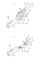
図1〜図3は本発明の第1実施形態を示す。図1(a)に示すように、圧着端子1は、相手端子(図示せず)との接続を行う相手端子接続部2と、電線Wを圧着する電線圧着部3とを備えている。圧着端子1は、所定形状に打ち抜かれた導電性部材を折り曲げ加工して作製される。
(First embodiment)
1 to 3 show a first embodiment of the present invention. As shown in FIG. 1A, the crimp terminal 1 includes a mating terminal connection portion 2 for connecting to a mating terminal (not shown) and a
相手端子接続部2は、方形枠体状であり、内部に弾性接触子(図示せず)を有する。相手端子(図示せず)は、この方形枠体内に進入して弾性接触子(図示せず)に接触する。 The mating terminal connection portion 2 has a rectangular frame shape, and has an elastic contact (not shown) inside. A mating terminal (not shown) enters the rectangular frame and contacts an elastic contact (not shown).
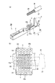
電線圧着部3は、基底部4とこの両側よりそれぞれ延設された一対の導体加締め部5から成る導体圧着部3Aと、基底部4とこの両側より延設された一対の外皮加締め部6から成る外皮圧着部3Bとを備えている。
The
導体圧着部3Aの基底部4と一対の導体加締め部5の内面には、図1(b)に詳しく示すように、円状のセレーション10a,10bが散在状態で多数設けられている。円状の各セレーション10a,10bは、基底部4と一対の導体加締め部5の内面より丸形状に窪む溝である。円状のセレーション10a,10bは、小さいサイズの小セレーション10aと大きなサイズの大セレーション10bの二種類である。小セレーション10aと大セレーション10bは、基底部4と一対の導体加締め部5の内面に、領域によって配置分けされている。つまり、小セレーション10aは、基底部4と一対の導体加締め部5の内面の電線引出し側のエリアE1に配置されている。大セレーション10bは、基底部4と一対の導体加締め部5の内面の電線引出し側とは反対側のエリアE2に配置されている。小セレーション10aと大セレーション10bは、それぞれ等間隔に散在されている。
As shown in detail in FIG. 1B, a large number of
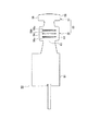
電線Wは、その端末箇所の外皮21が剥ぎ取られ、導体20が露出されている。そして、電線Wは、図2に示すように、一対の導体加締め部5の加締め変形によって導体20箇所が導体圧着部3Aで圧着され、一対の外被加締め部6の加締め変形によって外皮21箇所が外皮圧着部3Bで圧着されている。
As for the electric wire W, the
導体圧着部3A内の導体20は、図3(a)、(b)に示すように、一対の導体加締め部5の加締め過程の圧着力によって小セレーション10a及び大セレーション10bに食い込んでいる。
As shown in FIGS. 3A and 3B, the
以上説明したように、基底部4と一対の導体加締め部5の内面に円状のセレーション10a,10bを多数設けたので、従来例の線状のセレーションに較べてセレーション10a,10bのトータルエッジ長が長く、圧着時に導体20に生成される新生面の面積を大きくできる。これにより、導体圧着部3Aと導体20間の接触抵抗の安定化を確実に図ることができる。又、円状のセレーション10a,10bが多数設けられているので、従来例の線状のセレーションに較べてセレーション10a,10bのトータルの内部体積を大きくでき、導体20のセレーション10a,10bへのトータル食い込み体積が大きくなるため、引っ張り強度を確実に向上させることができる。以上より、導体20との間の接触抵抗の安定化と引っ張り強度の向上を共に確実に図ることができる。
As described above, since many
その上、セレーション10a,10bは、小さいサイズの小セレーション10aと大きいサイズの大セレーション10bの二種類である。そして、図3(a)に示すように、小セレーション10aを基底部4及び一対の導体加締め部5の電線引出し側のエリアE1に設け、図3(b)に示すように、大セレーション10bを基底部4及び一対の導体加締め部5の電線引出し側とは反対側のエリアE2に設けている。
In addition, the
ここで、電線Wから導体圧着部3Aに作用する引っ張り力は、導体圧着部3Aの電線引出側に先ず作用してここで受けるため、導体圧着部3Aの電線引出側のエリアE1が引っ張り強度の影響力が大きい側である。小セレーション10は、大セレーション10bに較べてセレーションエッジの導体20への剪断ダメージが小さいため、小セレーション10aのエリアE1では剪断ダメージによる電線Wの引っ張り強度の低下を防止できる。また、大セレーション10bは、小セレーション10aに較べてトータルエッジ長が長いため、大セレーション10のエリアE2では圧着時における新生面の生成面積が大きく増加する。従って、導体圧着部3Aの電線引出側の反対側では、接触抵抗が低い値で確実に安定化する。以上より、この第1実施形態では、導体20との間の接触抵抗の安定化と引っ張り強度の向上を共により確実に図ることができる。
Here, since the tensile force acting on the
(第2実施形態)
図4〜図6は本発明の第2実施形態を示す。この第2実施形態の圧着端子30は、前記第1実施形態のものと比較するに、小セレーション10aと大セレーション10bの配置分けの領域が相違する。つまり、図4(b)に詳しく示すように、導体圧着部3Aの領域は、導体圧着部3Aの電線Wの軸方向の直交方向(以下、幅方向)の中央エリアE3と、導体圧着部3Aの幅方向の一対の先端側のエリアE4とに分けられている。小セレーション10aは、中央エリアE3、つまり、ほぼ基底部4のエリアに配置されている。大セレーション10bは、一対の先端側のエリアE4、つまり、ほぼ一対の導体加締め部5のエリアに配置されている。小セレーション10aと大セレーション10bは、それぞれ等間隔に散在されている。
(Second Embodiment)
4 to 6 show a second embodiment of the present invention. The
他の構成は、前記第1実施形態と同様であるため、図面の同一構成箇所に同一符号を付して説明を省略する。 Since other configurations are the same as those of the first embodiment, the same reference numerals are given to the same components in the drawings, and description thereof will be omitted.
以上説明したように、基底部4と一対の導体加締め部5の内面に円状のセレーション10a,10bを多数設けたので、従来例の線状のセレーションに較べてセレーション10a,10bのトータルエッジ長が長く、圧着時に導体20に生成される新生面の面積を大きくできる。これにより、導体圧着部3Aと導体20間の接触抵抗の安定化を確実に図ることができる。又、円状のセレーション10a,10bが多数設けられているので、従来例の線状のセレーションに較べてセレーション10a,10bのトータルの内部体積を大きくでき、導体20のセレーション10a,10bへのトータル食い込み体積が大きくなるため、引っ張り強度を確実に向上させることができる。以上より、導体20との間の接触抵抗の安定化と引っ張り強度の向上を共に確実に図ることができる。
As described above, since many
その上、この第2実施形態では、導体圧着部3Aの幅方向の中央エリアE3に小セレーション10aを設け、導体圧着部3Aの幅方向の先端側に大セレーション10bを設けている。
In addition, in the second embodiment, the
ここで、導体圧着部3Aの圧着時には、一般的には導体20のセレーションへの入り込みが導体加締め部5側でスムーズではなく、セレーションエッジでの接触圧力が低下し、熱衝撃による導体20とSnメッキの線膨張係数の違いによる歪み差により新生面が破壊され、接触抵抗がばらつくおそれがある。しかし、この第2実施形態では、その箇所に大セレーション10bが設けられているため、セレーションエッジでの接触圧力を維持できる。従って、熱衝撃により破壊される新生面の面積を極力低減できるため、接触抵抗値を安定にできる。
Here, at the time of crimping the
また、圧着時において導体20とセレーションの底面との間に隙間が存在すると、酸化膜が生成し、その酸化膜が新生面同士で接触している部位にも成長し、これによって接触抵抗がばらつくおそれがある。しかし、基底部4に小セレーション10aが設けたので、圧着時において、導体20とセレーションの底面との間に発生する隙間を極力低減することができる。従って、酸化膜の生成と成長を抑制することができ、これによって接触抵抗を安定化できる。以上によって、接触抵抗を確実に安定化させることができる。
Further, if there is a gap between the
(その他)
第1及び第2実施形態において、セレーションのサイズによって導体20の変形状態、剪断ダメージ等を制御できることを利用して接触抵抗の安定化や引っ張り強度の向上を更に図る2つの実施形態を説明したが、これ以外のパターンも考えられる。
(Other)
In the first and second embodiments, two embodiments have been described in which the deformation state of the
又、セレーションのサイズは、二種類ではなく、三種類以上としても良い。セレーションを配置分けする領域もセレーションのサイズ数に応じてきめ細かく設定することが望ましい。 Further, the serration size may be three or more, not two. It is desirable that the area where the serrations are divided be set in detail according to the number of serration sizes.
小セレーション10a及び大セレーション10bの円形状とは、真円及びそれに類する形状を含む。又、小セレーション10aと大セレーション10bによって形状が異なっても良い。
The circular shape of the
1,30 圧着端子
3A 導体圧着部
4 基底部
5 導体加締め部
10a 小セレーション(セレーション)
10b 大セレーション(セレーション)
20 導体
1,30
10b Large serration (serration)
20 conductors
Claims (2)
前記基底部及び前記導体加締め部の内面に円状のセレーションを多数設け、前記セレーションは、小さいサイズの小セレーションと大きいサイズの大セレーションであり、
前記小セレーションは、前記基底部及び前記導体加締め部の電線引出し側のエリアに設け、前記大セレーションは、前記基底部及び前記導体加締め部の電線引出し側とは反対側のエリアに設けたことを特徴とする圧着端子。 A crimping terminal comprising a conductor crimping portion having a base portion and a conductor crimping portion that extends from a side of the base portion and crimps the conductor on the base portion,
A large number of circular serrations are provided on the inner surfaces of the base and the caulking portion of the conductor, and the serrations are small serrations of a small size and large serrations of a large size.
The small serration is provided in an area of the base portion and the conductor crimping portion on the side of the wire lead-out, and the large serration is provided in an area on the opposite side of the base portion and the conductor crimping portion of the wire lead-out side. Crimp terminal characterized by that.
前記基底部及び前記導体加締め部の内面に円状のセレーションを多数設け、前記セレーションは、小さいサイズの小セレーションと大きいサイズの大セレーションであり、
前記小セレーションは、前記基底部及び前記導体加締め部の幅方向の中央エリアに設け、前記大セレーションは、前記基底部及び前記導体加締め部の幅方向の先端側に設けたことを特徴とする圧着端子。
A crimping terminal comprising a conductor crimping portion having a base portion and a conductor crimping portion that extends from a side of the base portion and crimps the conductor on the base portion ,
A large number of circular serrations are provided on the inner surfaces of the base and the caulking portion of the conductor, and the serrations are small serrations of a small size and large serrations of a large size.
The small serration is provided in a central area in the width direction of the base portion and the conductor caulking portion, and the large serration is provided in a front end side in the width direction of the base portion and the conductor caulking portion. Crimp terminal to be used.
Priority Applications (5)
| Application Number | Priority Date | Filing Date | Title |
|---|---|---|---|
| JP2010175997A JP5675205B2 (en) | 2010-08-05 | 2010-08-05 | Crimp terminal |
| CN201180038586.5A CN103053078B (en) | 2010-08-05 | 2011-08-03 | Crimp type terminal |
| PCT/JP2011/067781 WO2012018050A1 (en) | 2010-08-05 | 2011-08-03 | Crimp terminal |
| EP11814675.2A EP2602877B1 (en) | 2010-08-05 | 2011-08-03 | Crimp terminal |
| US13/814,153 US9022818B2 (en) | 2010-08-05 | 2011-08-03 | Crimp terminal |
Applications Claiming Priority (1)
| Application Number | Priority Date | Filing Date | Title |
|---|---|---|---|
| JP2010175997A JP5675205B2 (en) | 2010-08-05 | 2010-08-05 | Crimp terminal |
Publications (2)
| Publication Number | Publication Date |
|---|---|
| JP2012038486A JP2012038486A (en) | 2012-02-23 |
| JP5675205B2 true JP5675205B2 (en) | 2015-02-25 |
Family
ID=45559546
Family Applications (1)
| Application Number | Title | Priority Date | Filing Date |
|---|---|---|---|
| JP2010175997A Active JP5675205B2 (en) | 2010-08-05 | 2010-08-05 | Crimp terminal |
Country Status (5)
| Country | Link |
|---|---|
| US (1) | US9022818B2 (en) |
| EP (1) | EP2602877B1 (en) |
| JP (1) | JP5675205B2 (en) |
| CN (1) | CN103053078B (en) |
| WO (1) | WO2012018050A1 (en) |
Families Citing this family (13)
| Publication number | Priority date | Publication date | Assignee | Title |
|---|---|---|---|---|
| JP5890992B2 (en) * | 2011-10-05 | 2016-03-22 | 矢崎総業株式会社 | Crimp terminal |
| JP5909345B2 (en) * | 2011-11-11 | 2016-04-26 | 矢崎総業株式会社 | Connector terminal |
| WO2014096898A1 (en) * | 2012-12-21 | 2014-06-26 | Delphi International Operations Luxembourg S.À.R.L. | Arrangement of an electrical wire and an electrical terminal sheet and method of manufacturing thereof |
| KR101824343B1 (en) * | 2013-10-15 | 2018-01-31 | 후루카와 에이에스 가부시키가이샤 | Terminal, wire harness, terminal and coated conductor wire connection method, and wire harness structure |
| JP2015079687A (en) | 2013-10-18 | 2015-04-23 | 矢崎総業株式会社 | Crimping terminal |
| JP6278675B2 (en) * | 2013-11-28 | 2018-02-14 | 日本航空電子工業株式会社 | Crimp terminal and connector |
| JP6514031B2 (en) * | 2015-05-19 | 2019-05-15 | 日本圧着端子製造株式会社 | Crimp terminal |
| JP6858552B2 (en) * | 2016-12-27 | 2021-04-14 | 矢崎総業株式会社 | Crimping terminal |
| JP6886814B2 (en) * | 2016-12-27 | 2021-06-16 | 矢崎総業株式会社 | Crimping terminal |
| JP2019114516A (en) * | 2017-12-26 | 2019-07-11 | 株式会社オートネットワーク技術研究所 | Wire with terminal |
| US11626671B2 (en) | 2019-08-29 | 2023-04-11 | J.S.T. Corporation | Electrical male terminal |
| US11043766B2 (en) * | 2019-08-29 | 2021-06-22 | J.S.T. Corporation | Electrical male terminal, and methods for connecting thereof |
| US11588255B2 (en) * | 2020-07-14 | 2023-02-21 | Yazaki Corporation | Electric wire with terminal having improved anticorrosion performance |
Family Cites Families (23)
| Publication number | Priority date | Publication date | Assignee | Title |
|---|---|---|---|---|
| US3831132A (en) * | 1971-04-29 | 1974-08-20 | Molex Inc | Crimp terminal for aluminum wire |
| US3892459A (en) * | 1974-06-21 | 1975-07-01 | Amp Inc | Open barrel terminal and method for terminating an electrical wire therein |
| US4003623A (en) | 1974-09-12 | 1977-01-18 | Amp Incorporated | Wire securing member with varying serrations |
| JPS6018104B2 (en) * | 1979-01-17 | 1985-05-08 | 住友電気工業株式会社 | Crimp terminal for aluminum conductor |
| JPS5842951B2 (en) | 1979-02-13 | 1983-09-22 | 住友電気工業株式会社 | Terminal crimping method for aluminum conductor wire |
| JPH02503726A (en) * | 1987-04-27 | 1990-11-01 | スタンデックス インターナショナル コーポレーション | magnetic wire connector clip |
| US7364479B1 (en) * | 2007-02-02 | 2008-04-29 | Pacesetter, Inc. | Crimp connector for connecting a conductor cable and electrode of an implantable cardiac electrotherapy lead |
| JP5103137B2 (en) * | 2007-11-01 | 2012-12-19 | 株式会社オートネットワーク技術研究所 | Crimp terminal, electric wire with terminal, and manufacturing method thereof |
| JP4922897B2 (en) | 2007-11-02 | 2012-04-25 | 株式会社オートネットワーク技術研究所 | Crimp terminal, electric wire with terminal, and manufacturing method thereof |
| JP5080291B2 (en) * | 2008-01-15 | 2012-11-21 | 株式会社オートネットワーク技術研究所 | Crimp terminal, electric wire with terminal, and manufacturing method thereof |
| JP5074984B2 (en) | 2008-03-31 | 2012-11-14 | 古河電気工業株式会社 | Crimp terminal |
| JP5006240B2 (en) * | 2008-03-31 | 2012-08-22 | 古河電気工業株式会社 | Crimp terminal |
| JP5400318B2 (en) * | 2008-04-15 | 2014-01-29 | 矢崎総業株式会社 | Crimp terminal for aluminum wire |
| JP5058082B2 (en) * | 2008-06-18 | 2012-10-24 | 株式会社オートネットワーク技術研究所 | Terminal fittings and electric wires with terminals |
| JP2010010001A (en) * | 2008-06-27 | 2010-01-14 | Autonetworks Technologies Ltd | Terminal metal fixture and wire with terminal |
| JP2010027464A (en) * | 2008-07-22 | 2010-02-04 | Sumitomo Wiring Syst Ltd | Terminal fitting and electric wire therewith |
| JP5071288B2 (en) * | 2008-07-22 | 2012-11-14 | 住友電装株式会社 | Terminal fittings and wires with terminal fittings |
| JP2010061870A (en) * | 2008-09-01 | 2010-03-18 | Sumitomo Wiring Syst Ltd | Terminal metal fitting, and electric wire with terminal metal fitting |
| JP5147648B2 (en) * | 2008-11-07 | 2013-02-20 | 矢崎総業株式会社 | Crimp terminal and wire fixing structure in crimp terminal |
| JP2010175997A (en) | 2009-01-30 | 2010-08-12 | Toshiba Corp | Electronic apparatus |
| EP2405690B1 (en) | 2009-03-03 | 2018-06-27 | Nec Corporation | Radio communication system, radio base station device, and method for controlling them |
| JP5634787B2 (en) * | 2010-08-04 | 2014-12-03 | 矢崎総業株式会社 | Crimp terminal |
| US8210884B2 (en) * | 2010-10-18 | 2012-07-03 | Tyco Electronics Corporation | Electrical terminal for terminating a wire |
-
2010
- 2010-08-05 JP JP2010175997A patent/JP5675205B2/en active Active
-
2011
- 2011-08-03 US US13/814,153 patent/US9022818B2/en active Active
- 2011-08-03 EP EP11814675.2A patent/EP2602877B1/en active Active
- 2011-08-03 CN CN201180038586.5A patent/CN103053078B/en active Active
- 2011-08-03 WO PCT/JP2011/067781 patent/WO2012018050A1/en active Application Filing
Also Published As
| Publication number | Publication date |
|---|---|
| US20130130570A1 (en) | 2013-05-23 |
| CN103053078A (en) | 2013-04-17 |
| JP2012038486A (en) | 2012-02-23 |
| EP2602877B1 (en) | 2016-03-09 |
| EP2602877A4 (en) | 2014-01-08 |
| WO2012018050A1 (en) | 2012-02-09 |
| EP2602877A1 (en) | 2013-06-12 |
| US9022818B2 (en) | 2015-05-05 |
| CN103053078B (en) | 2015-12-02 |
Similar Documents
| Publication | Publication Date | Title |
|---|---|---|
| JP5675205B2 (en) | Crimp terminal | |
| JP4922897B2 (en) | Crimp terminal, electric wire with terminal, and manufacturing method thereof | |
| JP3343880B2 (en) | Terminal fitting | |
| WO2010024033A1 (en) | Terminal metal fitting and method of manufacturing terminal metal fitting | |
| JP5074984B2 (en) | Crimp terminal | |
| JP2007287360A (en) | Spring female terminal | |
| JP2007184171A (en) | Female terminal with guidance strip | |
| JP2006344474A (en) | Female terminal fitting | |
| WO2015068650A1 (en) | Crimp terminal | |
| WO2016143466A1 (en) | Electric wire with terminal, and terminal | |
| WO2015053255A1 (en) | Crimp terminal | |
| JP5634789B2 (en) | Crimp terminal | |
| JP2010010000A (en) | Terminal metal fixture and wire with terminal | |
| JP5601925B2 (en) | Crimp terminal | |
| JP4894734B2 (en) | Terminal fitting | |
| JP2015076235A (en) | Crimping terminal | |
| JP2010044913A (en) | Crimp connection terminal | |
| JP2014007012A (en) | Crimp terminal | |
| JP7364394B2 (en) | Crimp terminals and wires with terminals | |
| WO2015068639A1 (en) | Crimp terminal | |
| JP5351539B2 (en) | Crimp terminal | |
| WO2015060161A1 (en) | Crimping terminal | |
| JP5342259B2 (en) | Crimp terminal | |
| JP5074983B2 (en) | Crimp terminal | |
| JP2015099639A (en) | Terminal metal fitting |
Legal Events
| Date | Code | Title | Description |
|---|---|---|---|
| A621 | Written request for application examination |
Free format text: JAPANESE INTERMEDIATE CODE: A621 Effective date: 20130716 |
|
| A131 | Notification of reasons for refusal |
Free format text: JAPANESE INTERMEDIATE CODE: A131 Effective date: 20140722 |
|
| A02 | Decision of refusal |
Free format text: JAPANESE INTERMEDIATE CODE: A02 Effective date: 20140930 |
|
| A521 | Request for written amendment filed |
Free format text: JAPANESE INTERMEDIATE CODE: A523 Effective date: 20141110 |
|
| A911 | Transfer to examiner for re-examination before appeal (zenchi) |
Free format text: JAPANESE INTERMEDIATE CODE: A911 Effective date: 20141201 |
|
| TRDD | Decision of grant or rejection written | ||
| A01 | Written decision to grant a patent or to grant a registration (utility model) |
Free format text: JAPANESE INTERMEDIATE CODE: A01 Effective date: 20141216 |
|
| A61 | First payment of annual fees (during grant procedure) |
Free format text: JAPANESE INTERMEDIATE CODE: A61 Effective date: 20141224 |
|
| R150 | Certificate of patent or registration of utility model |
Ref document number: 5675205 Country of ref document: JP Free format text: JAPANESE INTERMEDIATE CODE: R150 |
|
| R250 | Receipt of annual fees |
Free format text: JAPANESE INTERMEDIATE CODE: R250 |
|
| R250 | Receipt of annual fees |
Free format text: JAPANESE INTERMEDIATE CODE: R250 |
|
| R250 | Receipt of annual fees |
Free format text: JAPANESE INTERMEDIATE CODE: R250 |
|
| R250 | Receipt of annual fees |
Free format text: JAPANESE INTERMEDIATE CODE: R250 |
|
| R250 | Receipt of annual fees |
Free format text: JAPANESE INTERMEDIATE CODE: R250 |
|
| R250 | Receipt of annual fees |
Free format text: JAPANESE INTERMEDIATE CODE: R250 |
|
| S531 | Written request for registration of change of domicile |
Free format text: JAPANESE INTERMEDIATE CODE: R313531 |
|
| R350 | Written notification of registration of transfer |
Free format text: JAPANESE INTERMEDIATE CODE: R350 |
|
| R250 | Receipt of annual fees |
Free format text: JAPANESE INTERMEDIATE CODE: R250 |