JP5668345B2 - Optical filter, optical filter module, spectrophotometer and optical instrument - Google Patents
Optical filter, optical filter module, spectrophotometer and optical instrument Download PDFInfo
- Publication number
- JP5668345B2 JP5668345B2 JP2010158876A JP2010158876A JP5668345B2 JP 5668345 B2 JP5668345 B2 JP 5668345B2 JP 2010158876 A JP2010158876 A JP 2010158876A JP 2010158876 A JP2010158876 A JP 2010158876A JP 5668345 B2 JP5668345 B2 JP 5668345B2
- Authority
- JP
- Japan
- Prior art keywords
- wavelength
- filter
- bandpass filter
- optical
- substrate
- Prior art date
- Legal status (The legal status is an assumption and is not a legal conclusion. Google has not performed a legal analysis and makes no representation as to the accuracy of the status listed.)
- Active
Links
- 230000003287 optical effect Effects 0.000 title claims description 107
- 239000012788 optical film Substances 0.000 claims description 145
- 239000000758 substrate Substances 0.000 claims description 127
- 230000003595 spectral effect Effects 0.000 claims description 91
- BJQHLKABXJIVAM-UHFFFAOYSA-N bis(2-ethylhexyl) phthalate Chemical compound CCCCC(CC)COC(=O)C1=CC=CC=C1C(=O)OCC(CC)CCCC BJQHLKABXJIVAM-UHFFFAOYSA-N 0.000 claims description 68
- 238000012545 processing Methods 0.000 claims description 45
- 239000000463 material Substances 0.000 claims description 9
- 238000001228 spectrum Methods 0.000 claims description 5
- 238000005259 measurement Methods 0.000 description 71
- 239000010408 film Substances 0.000 description 42
- PXKLMJQFEQBVLD-UHFFFAOYSA-N bisphenol F Chemical compound C1=CC(O)=CC=C1CC1=CC=C(O)C=C1 PXKLMJQFEQBVLD-UHFFFAOYSA-N 0.000 description 32
- 238000000034 method Methods 0.000 description 28
- 230000005540 biological transmission Effects 0.000 description 22
- 238000010586 diagram Methods 0.000 description 18
- 230000001360 synchronised effect Effects 0.000 description 18
- 238000006243 chemical reaction Methods 0.000 description 12
- 239000011521 glass Substances 0.000 description 10
- 230000008859 change Effects 0.000 description 8
- 102100040862 Dual specificity protein kinase CLK1 Human genes 0.000 description 7
- 101000749294 Homo sapiens Dual specificity protein kinase CLK1 Proteins 0.000 description 7
- 238000004364 calculation method Methods 0.000 description 7
- 238000004891 communication Methods 0.000 description 7
- 102100040844 Dual specificity protein kinase CLK2 Human genes 0.000 description 4
- 101000749291 Homo sapiens Dual specificity protein kinase CLK2 Proteins 0.000 description 4
- VYPSYNLAJGMNEJ-UHFFFAOYSA-N Silicium dioxide Chemical compound O=[Si]=O VYPSYNLAJGMNEJ-UHFFFAOYSA-N 0.000 description 4
- GWEVSGVZZGPLCZ-UHFFFAOYSA-N Titan oxide Chemical compound O=[Ti]=O GWEVSGVZZGPLCZ-UHFFFAOYSA-N 0.000 description 4
- 238000013461 design Methods 0.000 description 4
- 230000006870 function Effects 0.000 description 4
- 238000004519 manufacturing process Methods 0.000 description 4
- 238000002834 transmittance Methods 0.000 description 4
- 229910004298 SiO 2 Inorganic materials 0.000 description 3
- 238000004458 analytical method Methods 0.000 description 3
- 239000000470 constituent Substances 0.000 description 3
- 230000000694 effects Effects 0.000 description 3
- 230000008569 process Effects 0.000 description 3
- ZLMJMSJWJFRBEC-UHFFFAOYSA-N Potassium Chemical compound [K] ZLMJMSJWJFRBEC-UHFFFAOYSA-N 0.000 description 2
- 229910010413 TiO 2 Inorganic materials 0.000 description 2
- 238000004737 colorimetric analysis Methods 0.000 description 2
- 238000005530 etching Methods 0.000 description 2
- 238000012986 modification Methods 0.000 description 2
- 230000004048 modification Effects 0.000 description 2
- 239000013307 optical fiber Substances 0.000 description 2
- 238000006116 polymerization reaction Methods 0.000 description 2
- 229910052700 potassium Inorganic materials 0.000 description 2
- 239000011591 potassium Substances 0.000 description 2
- 230000001681 protective effect Effects 0.000 description 2
- 239000011734 sodium Substances 0.000 description 2
- 239000007787 solid Substances 0.000 description 2
- 238000004611 spectroscopical analysis Methods 0.000 description 2
- OGIDPMRJRNCKJF-UHFFFAOYSA-N titanium oxide Inorganic materials [Ti]=O OGIDPMRJRNCKJF-UHFFFAOYSA-N 0.000 description 2
- 229910001316 Ag alloy Inorganic materials 0.000 description 1
- DGAQECJNVWCQMB-PUAWFVPOSA-M Ilexoside XXIX Chemical compound C[C@@H]1CC[C@@]2(CC[C@@]3(C(=CC[C@H]4[C@]3(CC[C@@H]5[C@@]4(CC[C@@H](C5(C)C)OS(=O)(=O)[O-])C)C)[C@@H]2[C@]1(C)O)C)C(=O)O[C@H]6[C@@H]([C@H]([C@@H]([C@H](O6)CO)O)O)O.[Na+] DGAQECJNVWCQMB-PUAWFVPOSA-M 0.000 description 1
- CDBYLPFSWZWCQE-UHFFFAOYSA-L Sodium Carbonate Chemical compound [Na+].[Na+].[O-]C([O-])=O CDBYLPFSWZWCQE-UHFFFAOYSA-L 0.000 description 1
- 239000003513 alkali Substances 0.000 description 1
- 229910052783 alkali metal Inorganic materials 0.000 description 1
- 150000001340 alkali metals Chemical class 0.000 description 1
- 239000002585 base Substances 0.000 description 1
- 230000008901 benefit Effects 0.000 description 1
- 239000005388 borosilicate glass Substances 0.000 description 1
- 229910052681 coesite Inorganic materials 0.000 description 1
- 229910052906 cristobalite Inorganic materials 0.000 description 1
- 239000013078 crystal Substances 0.000 description 1
- 230000007423 decrease Effects 0.000 description 1
- 230000001934 delay Effects 0.000 description 1
- 238000000605 extraction Methods 0.000 description 1
- 238000010030 laminating Methods 0.000 description 1
- 239000010410 layer Substances 0.000 description 1
- 239000005355 lead glass Substances 0.000 description 1
- 230000009467 reduction Effects 0.000 description 1
- 239000000377 silicon dioxide Substances 0.000 description 1
- 235000012239 silicon dioxide Nutrition 0.000 description 1
- 229910052814 silicon oxide Inorganic materials 0.000 description 1
- 239000002356 single layer Substances 0.000 description 1
- 229910052708 sodium Inorganic materials 0.000 description 1
- 238000004544 sputter deposition Methods 0.000 description 1
- 229910052682 stishovite Inorganic materials 0.000 description 1
- 229910052905 tridymite Inorganic materials 0.000 description 1
Images


Classifications
-
- G—PHYSICS
- G02—OPTICS
- G02B—OPTICAL ELEMENTS, SYSTEMS OR APPARATUS
- G02B26/00—Optical devices or arrangements for the control of light using movable or deformable optical elements
- G02B26/001—Optical devices or arrangements for the control of light using movable or deformable optical elements based on interference in an adjustable optical cavity
-
- G—PHYSICS
- G01—MEASURING; TESTING
- G01J—MEASUREMENT OF INTENSITY, VELOCITY, SPECTRAL CONTENT, POLARISATION, PHASE OR PULSE CHARACTERISTICS OF INFRARED, VISIBLE OR ULTRAVIOLET LIGHT; COLORIMETRY; RADIATION PYROMETRY
- G01J3/00—Spectrometry; Spectrophotometry; Monochromators; Measuring colours
- G01J3/12—Generating the spectrum; Monochromators
- G01J3/26—Generating the spectrum; Monochromators using multiple reflection, e.g. Fabry-Perot interferometer, variable interference filters
-
- G—PHYSICS
- G01—MEASURING; TESTING
- G01J—MEASUREMENT OF INTENSITY, VELOCITY, SPECTRAL CONTENT, POLARISATION, PHASE OR PULSE CHARACTERISTICS OF INFRARED, VISIBLE OR ULTRAVIOLET LIGHT; COLORIMETRY; RADIATION PYROMETRY
- G01J3/00—Spectrometry; Spectrophotometry; Monochromators; Measuring colours
- G01J3/46—Measurement of colour; Colour measuring devices, e.g. colorimeters
- G01J3/50—Measurement of colour; Colour measuring devices, e.g. colorimeters using electric radiation detectors
- G01J3/51—Measurement of colour; Colour measuring devices, e.g. colorimeters using electric radiation detectors using colour filters
- G01J3/513—Measurement of colour; Colour measuring devices, e.g. colorimeters using electric radiation detectors using colour filters having fixed filter-detector pairs
Description
本発明は、光フィルター、光フィルターモジュール、分光測定器および光機器等に関する。 The present invention relates to an optical filter, an optical filter module, a spectrometer, an optical device, and the like.
干渉フィルターは従来から分光測定器等に用いられている。干渉フィルターの一態様として、透過波長を可変に制御する干渉フィルター(ファブリペローエタロン干渉フィルター)が知られている(例えば、特許文献1参照)。特許文献1に記載される、透過波長が可変である透過波長可変干渉フィルターでは、互いに平行に保持された一対の基板と、この一対の基板上に互いに対向すると共に一定間隔のギャップを有するように形成された一対の多層膜(光学膜)とを備え、外力により一対の多層膜(光学膜)間のギャップ(干渉ギャップ)の大きさを変化させて、透過波長を可変に制御している。
Conventionally, interference filters have been used in spectroscopic instruments. As an aspect of the interference filter, an interference filter (Fabry-Perot etalon interference filter) that variably controls the transmission wavelength is known (see, for example, Patent Document 1). In the transmission wavelength variable interference filter described in
しかし、所望波長帯域を一つの波長可変フィルター(例えば可変ギャップエタロンフィルター)でカバーし、例えばnポイント(nは2以上の整数)で分光測定を行う場合、波長可変フィルターの多層膜(光学膜)間のギャップの大きさを変える必要がある。詳しくは、ギャップの大きさを変えて各測定ポイントに対応した分光帯域を実現し、次に、その分光帯域における測定を実施する、という動作を、測定ポイントの数だけ繰り返す必要がある。よって、所望波長帯域の帯域幅が広くなると、必要な測定データをすべて取得するための測定時間が長くなる。つまり、波長可変フィルターが、所望波長帯域の全帯域をスキャンするのに要する時間が長くなるという課題が生じる。 However, when the desired wavelength band is covered with a single wavelength tunable filter (for example, a variable gap etalon filter), for example, when performing spectroscopic measurement at n points (n is an integer of 2 or more), a multilayer film (optical film) of the wavelength tunable filter It is necessary to change the size of the gap between them. Specifically, it is necessary to repeat the operation of realizing the spectral band corresponding to each measurement point by changing the size of the gap and then performing the measurement in the spectral band by the number of measurement points. Therefore, as the bandwidth of the desired wavelength band becomes wider, the measurement time for acquiring all necessary measurement data becomes longer. That is, there arises a problem that the time required for the wavelength tunable filter to scan the entire desired wavelength band becomes longer.
本発明の少なくとも一つの態様によれば、例えば、波長可変フィルターが、所望波長帯域の全帯域をスキャンするのに要する時間を短縮することができる。 According to at least one aspect of the present invention, for example, the time required for the wavelength tunable filter to scan the entire desired wavelength band can be shortened.
(1)本発明の光フィルターの一態様では、第1波長可変バンドパスフィルターと、第2波長可変バンドパスフィルターと、前記第1波長可変バンドパスフィルターおよび前記第2波長可変バンドパスフィルターの各々を駆動する駆動部と、前記第1波長可変バンドパスフィルターおよび前記第2波長可変バンドパスフィルターの各々の分光帯域を可変に制御する制御部と、を含み、前記第1波長可変バンドパスフィルターは、所望波長帯域における第1波長帯域の光を分光可能であり、かつ、分光帯域として、前記第1波長帯域内の第1波長を中心波長とする第1分光帯域と、前記第1波長帯域内の第2波長を中心波長とする第2分光帯域と、を少なくとも有し、前記第2波長可変バンドパスフィルターは、前記所望波長帯域における、前記第1波長帯域に隣接する第2波長帯域の光を分光可能であり、かつ、分光帯域として、前記第2波長帯域内の第3波長を中心波長とする第3分光帯域と、前記第2波長帯域内の第4波長を中心波長とする第4分光帯域と、を少なくとも有し、前記駆動部は、前記第1波長可変バンドパスフィルターおよび前記第2波長可変バンドパスフィルターの各々を共に駆動し、前記第1波長可変バンドパスフィルターに前記第1分光帯域の光が分光される期間と、前記第2波長可変バンドパスフィルターに前記第3分光帯域の光が分光される期間の少なくとも一部が重複し、かつ、前記第1波長可変バンドパスフィルターに前記第2分光帯域の光が分光される期間と、前記第2波長可変バンドパスフィルターに前記第4分光帯域の光が分光される期間の少なくとも一部が重複する。 (1) In one aspect of the optical filter of the present invention, each of the first wavelength tunable bandpass filter, the second wavelength tunable bandpass filter, the first wavelength tunable bandpass filter, and the second wavelength tunable bandpass filter And a controller that variably controls a spectral band of each of the first wavelength tunable bandpass filter and the second wavelength tunable bandpass filter, and the first wavelength tunable bandpass filter includes: The first wavelength band in the desired wavelength band can be dispersed, and as the spectral band, a first spectral band having the first wavelength in the first wavelength band as a central wavelength, and in the first wavelength band A second spectral band centered on the second wavelength of the second wavelength band, and the second wavelength tunable bandpass filter includes a first spectral band in the desired wavelength band. A second spectral band that can disperse light in a second wavelength band adjacent to the first wavelength band, and that has a third wavelength in the second wavelength band as a central wavelength, and the second wavelength; At least a fourth spectral band having a fourth wavelength in the band as a center wavelength, and the driving unit drives each of the first wavelength tunable bandpass filter and the second wavelength tunable bandpass filter together. , At least a part of a period in which the light in the first spectral band is split into the first wavelength variable bandpass filter and a period in which the light in the third spectral band is split into the second wavelength variable bandpass filter. A period in which the light in the second spectral band is split into the first wavelength tunable bandpass filter and a period in which the light in the fourth spectral band is split into the second wavelength tunable bandpass filter. At least partially overlap.
本態様では、所望波長帯域を一つの波長可変フィルターでカバーするのではなく、複数の(つまり2以上の)波長可変バンドパスフィルターを用いてカバーすると共に、各波長可変バンドパスフィルターを並行して駆動する。 In this embodiment, a desired wavelength band is not covered by a single tunable filter, but is covered with a plurality of (that is, two or more) tunable bandpass filters, and each tunable bandpass filter is parallelized. To drive.
波長可変バンドパスフィルターは、一つの光学フィルターで、実質的に複数の分光帯域を実現することができ、簡易な構成で広い波長域をカバーでき、使い勝手がよいという特性を有する。この波長可変バンドパスフィルターを複数個使用し、各フィルターに分光する帯域を割り当てることによって、各フィルターの負担が軽減され、かつ、各フィルターを並行して駆動することによって、効率的な波長スキャンが実現される。すなわち、複数の波長可変バンドパスフィルター(少なくとも第1波長可変バンドパスフィルターおよび第2波長可変バンドパスフィルターを含む)の並行駆動によって、各フィルターの分光処理期間の少なくとも一部が時間軸上で重複し、したがって、所望波長帯域の全帯域をスキャンするのに要する時間を短縮することができる。例えば、n個の波長可変バンドパスフィルターを同時に駆動する場合、所望波長帯域の全帯域をスキャンするのに要する時間は、例えば、従来の1/nに短縮される。よって、例えば、広い範囲の波長域を効率的にカバー可能な光フィルターが実現される。 The wavelength tunable bandpass filter has a characteristic that it can realize substantially a plurality of spectral bands with one optical filter, can cover a wide wavelength range with a simple configuration, and is easy to use. By using multiple wavelength tunable bandpass filters and assigning spectral bands to each filter, the burden on each filter is reduced, and driving each filter in parallel enables efficient wavelength scanning. Realized. That is, by parallel driving of a plurality of wavelength tunable bandpass filters (including at least the first wavelength tunable bandpass filter and the second wavelength tunable bandpass filter), at least a part of the spectral processing period of each filter overlaps on the time axis. Therefore, the time required to scan the entire band of the desired wavelength band can be shortened. For example, when n wavelength tunable bandpass filters are driven simultaneously, the time required to scan the entire desired wavelength band is reduced to, for example, 1 / n of the conventional one. Therefore, for example, an optical filter capable of efficiently covering a wide wavelength range is realized.
また、複数の波長可変バンドパスフィルターが、各々に割り当てられた波長帯域を分光することによって、個々の波長可変バンドパスフィルターの可動部の可動範囲が抑制され、アクチュエーターの駆動電圧の上昇を抑制することができる。よって、駆動回路(駆動部)を構築するのが容易となり、消費電力の削減も可能である。 In addition, a plurality of wavelength tunable bandpass filters divide the wavelength band assigned to each, thereby suppressing the movable range of the movable part of each wavelength tunable bandpass filter and suppressing an increase in the drive voltage of the actuator. be able to. Therefore, it is easy to construct a drive circuit (drive unit), and power consumption can be reduced.
また、例えば、各波長可変バンドパスフィルターに使用される光学膜(例えば、屈折率の異なる膜を積層した構造をもち、光の反射特性と透過特性とを併せ持つ光学膜)を簡素化することができる。このことは、光フィルターの構成の簡素化に役立つ。 In addition, for example, an optical film used for each wavelength variable bandpass filter (for example, an optical film having a structure in which films having different refractive indexes are stacked and having both light reflection characteristics and transmission characteristics) can be simplified. it can. This helps to simplify the configuration of the optical filter.
(2)本発明の光フィルターの他の態様では、前記第1波長可変バンドパスフィルターおよび前記第2波長可変バンドパスフィルターは、可変ギャップエタロンフィルターで構成され、前記第1波長可変バンドパスフィルターのギャップを第1ギャップとし、前記第2波長可変バンドパスフィルターのギャップを第2ギャップとした場合に、前記第1ギャップおよび前記2ギャップの、前記第1波長可変バンドパスフィルターおよび前記第2波長可変バンドパスフィルターの駆動開始時における初期ギャップ値は同じ値であり、かつ、前記駆動部は、第1駆動電圧によって前記第1波長可変フィルターを駆動し、前記第1駆動電圧とは異なる値の第2駆動電圧によって前記第2波長可変フィルターを駆動する。 (2) In another aspect of the optical filter of the present invention, the first wavelength tunable bandpass filter and the second wavelength tunable bandpass filter are configured by a variable gap etalon filter, and the first wavelength tunable bandpass filter includes: When the gap is the first gap and the second wavelength tunable bandpass filter is the second gap, the first wavelength tunable bandpass filter and the second wavelength tunable of the first gap and the two gaps. The initial gap value at the start of driving the bandpass filter is the same value, and the driving unit drives the first wavelength tunable filter with the first driving voltage, and the first driving voltage has a value different from the first driving voltage. The second wavelength tunable filter is driven by two driving voltages.
本態様では、複数の波長可変バンドパスフィルターの各々の初期ギャップ値は同じ値に設定されており、各フィルターに、異なるレベルの駆動電圧を印加することによって、各フィルターのギャップを個別に制御する。これによって、各フィルターのギャップは異なる値となり、各フィルターにおいて、所望波長の分光帯域が実現される。ここで、波長可変バンドパスフィルターの初期ギャップ値とは、駆動電圧を印加しない状態のギャップの大きさをいう。本態様では、各フィルターに、異なる電圧を印加することができる。よって、仮に各フィルターの特性がばらついたとしても、そのばらつきを補償するように駆動電圧を調整する(微調整する)ことができる。各フィルターに最適な駆動電圧が印加されるため、各フィルターの分光帯域の精度が向上する。 In this aspect, the initial gap value of each of the plurality of wavelength tunable bandpass filters is set to the same value, and the gap of each filter is individually controlled by applying different levels of driving voltages to each filter. . Thereby, the gap of each filter becomes a different value, and a spectral band of a desired wavelength is realized in each filter. Here, the initial gap value of the wavelength tunable bandpass filter refers to the size of the gap in a state where no drive voltage is applied. In this aspect, a different voltage can be applied to each filter. Therefore, even if the characteristics of each filter vary, the drive voltage can be adjusted (finely adjusted) to compensate for the variation. Since the optimum drive voltage is applied to each filter, the accuracy of the spectral band of each filter is improved.
また、各フィルターの駆動電圧が異なるため、電圧印加時に生じるオーバーシュート(ならびにアンダーシュート)の周期に差が生じる。各駆動電圧の揺れが重畳されると、大きなノイズが生じて、例えば、駆動部における基準電位(グランドGNDや電源電位VDD)に大きな変動が生じる場合がある。本態様では、各駆動電圧の揺れの周期が異なることからノイズが分散され、よって、大きなノイズが生じにくくなる。また、フィルター毎に、駆動電圧を調整することができるため、例えば、駆動電圧のレベルを切り換える場合における、1回の切り換え当たりの電圧の変化量を、小さく抑制するといった微調整も行い易くなる。この場合、電圧切り換え時における、駆動電圧のオーバーシュートを抑制することができる。 In addition, since the drive voltages of the filters are different, a difference occurs in the period of overshoot (and undershoot) that occurs when a voltage is applied. When fluctuations of the drive voltages are superimposed, a large noise is generated, and for example, a large fluctuation may occur in the reference potential (ground GND or power supply potential VDD) in the drive unit. In this aspect, since the period of fluctuation of each drive voltage is different, noise is dispersed, and therefore, large noise is less likely to occur. Further, since the drive voltage can be adjusted for each filter, for example, when the level of the drive voltage is switched, it becomes easy to perform fine adjustment such as suppressing the amount of change in voltage per switching small. In this case, overshoot of the drive voltage at the time of voltage switching can be suppressed.
(3)本発明の光フィルターの他の態様では、前記第1波長可変バンドパスフィルターおよび前記第2波長可変バンドパスフィルターは、可変ギャップエタロンフィルターで構成され、前記第1波長可変バンドパスフィルターのギャップを第1ギャップとし、前記第2波長可変バンドパスフィルターのギャップを第2ギャップとした場合に、前記第1ギャップおよび前記2ギャップの、前記第1波長可変バンドパスフィルターおよび前記第2波長可変バンドパスフィルターの駆動開始時における初期ギャップ値が異なる値であり、かつ、前記駆動部は、第1駆動電圧によって前記第1波長可変フィルターを駆動し、前記第1駆動電圧と同じ値の第2駆動電圧によって前記第2波長可変フィルターを駆動する。 (3) In another aspect of the optical filter of the present invention, the first wavelength tunable bandpass filter and the second wavelength tunable bandpass filter are configured by a variable gap etalon filter, and the first wavelength tunable bandpass filter includes: When the gap is the first gap and the second wavelength tunable bandpass filter is the second gap, the first wavelength tunable bandpass filter and the second wavelength tunable of the first gap and the two gaps. The initial gap value at the start of driving the bandpass filter is a different value, and the driving unit drives the first wavelength tunable filter with a first driving voltage, and a second value having the same value as the first driving voltage. The second wavelength tunable filter is driven by a driving voltage.
本態様では、複数の波長可変バンドパスフィルターの各々の初期ギャップ値は異なる値に設定されている。つまり、各フィルターが分光する帯域の、一端側の波長に対応するギャップ値が選択されている。この状態で、各フィルターに、同じレベルの駆動電圧を印加することによって、各フィルターのギャップを変化させて、フィルター毎に、分光帯域の波長を切り換える。 In this aspect, the initial gap value of each of the plurality of wavelength tunable bandpass filters is set to a different value. That is, the gap value corresponding to the wavelength on one end side of the band in which each filter separates is selected. In this state, by applying the same level of drive voltage to each filter, the gap of each filter is changed, and the wavelength of the spectral band is switched for each filter.
本態様によれば、各フィルターの駆動電圧を共通化することができる。よって、制御部に設けられる、電圧設定メモリーに設定される駆動電圧値の数が減少する。n個の波長可変バンドパスフィルターを使用する場合、設定電圧数は1/nとなる。したがって、電圧設定メモリーのメモリー領域が少なくて済む。メモリー容量を低減できることから、メモリーの専有面積が減少し、小型化に有利となり、また、例えば、電圧設定メモリーとして、低コストのROM等を使用することもできる。また、駆動電圧のレベルを切り換える場合における、1回の切り換え当たりの電圧変化量がそれほど大きくなければ、駆動電圧切り換え時におけるノイズはそれほど問題とはならない。 According to this aspect, the drive voltage of each filter can be made common. Therefore, the number of drive voltage values set in the voltage setting memory provided in the control unit is reduced. When n wavelength variable bandpass filters are used, the number of set voltages is 1 / n. Therefore, the memory area of the voltage setting memory can be reduced. Since the memory capacity can be reduced, the area occupied by the memory is reduced, which is advantageous for downsizing. For example, a low-cost ROM or the like can be used as the voltage setting memory. In addition, when switching the drive voltage level, if the amount of voltage change per switching is not so large, noise during switching of the driving voltage is not a problem.
(4)本発明の光フィルターの他の態様では、前記第1波長可変バンドパスフィルターは、第1基板と、前記第1基板と対向する第2基板と、前記第1基板に設けられた第1光学膜と、前記第2基板に設けられ、前記第1光学膜と対向する第2光学膜と、前記第1基板に設けられ、前記第1基板の厚み方向からみた平面視において、前記第1光学膜の周囲に形成された第1電極と、前記第2基板に設けられ、前記第2基板の厚み方向からみた平面視において、前記第2光学膜の周囲に形成された第2電極と、を有し、前記第1電極と前記第2電極との間の静電力によって、前記第1光学膜と前記第2光学膜との間の前記第1ギャップが制御されて前記第1分光帯域および前記第2分光帯域の光を分光可能であり、前記第2波長可変バンドパスフィルターは、第3基板と、前記第3基板と対向する第4基板と、前記第3基板に設けられた第3光学膜と、前記第4基板に設けられ、前記第3光学膜と対向する第4光学膜と、前記第3基板に設けられ、前記第3基板の厚み方向からみた平面視において、前記第3光学膜の周囲に形成された第3電極と、前記第4基板に設けられ、前記第4基板の厚み方向からみた平面視において、前記第4光学膜の周囲に形成された第4電極と、を有し、前記第3電極と前記第4電極との間の静電力によって、前記第3光学膜と前記第4光学膜との間の前記第2ギャップが制御されて前記第3分光帯域または前記第4分光帯域の光を分光可能である。 (4) In another aspect of the optical filter of the present invention, the first wavelength tunable bandpass filter includes a first substrate, a second substrate facing the first substrate, and a first substrate provided on the first substrate. A first optical film, a second optical film provided on the second substrate and opposed to the first optical film, and provided on the first substrate, in plan view as viewed from a thickness direction of the first substrate, the first optical film; A first electrode formed around one optical film; and a second electrode provided on the second substrate and formed around the second optical film in a plan view as viewed from the thickness direction of the second substrate; The first spectral band is controlled by controlling the first gap between the first optical film and the second optical film by an electrostatic force between the first electrode and the second electrode. And the second wavelength tunable bandpass capable of dispersing light in the second spectral band. The filter is provided on the third substrate, on the fourth substrate facing the third substrate, on the third optical film provided on the third substrate, and on the fourth substrate facing the third optical film. A fourth optical film, provided on the third substrate, and provided on the fourth substrate; a third electrode formed around the third optical film in a plan view as viewed from a thickness direction of the third substrate; A fourth electrode formed around the fourth optical film in a plan view as viewed from the thickness direction of the fourth substrate, and by an electrostatic force between the third electrode and the fourth electrode. The second gap between the third optical film and the fourth optical film is controlled so that the light in the third spectral band or the fourth spectral band can be dispersed.
本態様では、第1波長可変バンドパスフィルターおよび第2波長可変バンドパスフィルターとして、静電駆動式の可変ギャップエタロンフィルター(以下、単に、可変ギャップエタロンという場合があり、また、単にフィルターという場合もある)を使用する。第1波長可変バンドパスフィルターは、第1基板(例えば固定基板)と、第1基板に対向して配置される第2基板(例えば可動基板)とを有する。第1基板(例えば固定基板)には、第1光学膜が形成され、その周囲に静電アクチュエーターの構成要素である第1電極が形成されている。第2基板(例えば可動基板)には、第2光学膜が形成され、その周囲には静電アクチュエーターの構成要素である第2電極が形成されている。第2光学膜は、例えば第1光学膜と対向して配置され、その周囲において、例えば第1電極に対向するように第2電極が形成されている。第1光学膜と第2光学膜は、干渉計の構成要素である反射膜としての機能を有する。第1電極と第2電極との間に所定の電位差が生じると、電極間に例えば静電力(例えば静電引力)が生じる。例えば可動基板である第2基板は可撓性を有しており、第2基板に、静電力による撓みが生じ、第1光学膜と第2光学膜との間のギャップ(干渉ギャップ)の大きさが変化し(例えば縮小し)、可変ギャップエタロンフィルターの光透過帯域(つまり分光帯域)が変化する。 In this aspect, the first wavelength tunable bandpass filter and the second wavelength tunable bandpass filter may be electrostatically driven variable gap etalon filters (hereinafter simply referred to as variable gap etalons, or simply referred to as filters). Use). The first wavelength tunable bandpass filter includes a first substrate (for example, a fixed substrate) and a second substrate (for example, a movable substrate) disposed to face the first substrate. A first optical film is formed on a first substrate (for example, a fixed substrate), and a first electrode that is a component of an electrostatic actuator is formed around the first optical film. A second optical film is formed on a second substrate (for example, a movable substrate), and a second electrode that is a component of the electrostatic actuator is formed around the second optical film. For example, the second optical film is disposed so as to face the first optical film, and the second electrode is formed around the second optical film so as to face the first electrode, for example. The first optical film and the second optical film have a function as a reflective film that is a component of the interferometer. When a predetermined potential difference is generated between the first electrode and the second electrode, for example, an electrostatic force (for example, electrostatic attractive force) is generated between the electrodes. For example, the second substrate, which is a movable substrate, has flexibility, and the second substrate bends due to electrostatic force, so that the gap (interference gap) between the first optical film and the second optical film is large. Changes (for example, shrinks), and the light transmission band (that is, spectral band) of the variable gap etalon filter changes.
第2波長可変バンドパスフィルターの構成と動作も同様である。つまり、第2波長可変バンドパスフィルターは、第3基板(例えば固定基板)と、第3基板に対向して配置される第4基板(例えば可動基板)とを有する。第3基板(例えば固定基板)には、第3光学膜が形成され、その周囲に静電アクチュエーターの構成要素である第3電極が形成されている。第4基板(例えば可動基板)には、第4光学膜が形成され、その周囲に静電アクチュエーターの構成要素である第4電極が形成されている。第4光学膜は第3光学膜と対向して配置され、その周囲において、例えば第3電極と対向するように第4電極が形成されている。第3光学膜と第4光学膜は、干渉計の構成要素である反射膜としての機能を有する。 The configuration and operation of the second wavelength tunable bandpass filter are the same. That is, the second wavelength tunable bandpass filter includes a third substrate (for example, a fixed substrate) and a fourth substrate (for example, a movable substrate) disposed to face the third substrate. A third optical film is formed on a third substrate (for example, a fixed substrate), and a third electrode that is a component of the electrostatic actuator is formed around the third optical film. A fourth optical film is formed on a fourth substrate (for example, a movable substrate), and a fourth electrode that is a component of the electrostatic actuator is formed around the fourth optical film. The fourth optical film is disposed to face the third optical film, and a fourth electrode is formed around the fourth optical film so as to face the third electrode, for example. The third optical film and the fourth optical film have a function as a reflective film that is a component of the interferometer.
可変ギャップエタロンフィルターは、ファブリペロー干渉計の原理を利用した、構成が簡易で、小型化、低価格に適した波長可変フィルターであり、本態様では、この可変ギャップエタロンフィルターを複数使用して、各フィルターの各々に異なる波長帯域を分光させる。波長可変フィルターを複数用いることによって、1つのフィルターにおけるアクチュエーターの可動範囲が狭くなり、よって、駆動電圧を低減でき(省電力効果)、ならびに、1回の駆動電圧の変化量が小さくなることから、駆動電圧を大きく変化させる場合に比べて、駆動電圧の精度が向上するという効果を得ることができる。また、光学膜の設計も容易化される。よって、設計負荷ならびにプロセス負荷を低減することが可能となる。よって、例えば、簡素化された構成を備え、小型軽量で、広い波長範囲を効率的にカバー可能な、使い勝手のよい光フィルターを実現することができる。 The variable gap etalon filter is a wavelength tunable filter that uses the principle of the Fabry-Perot interferometer, has a simple structure, is small in size, and is suitable for low cost.In this aspect, a plurality of variable gap etalon filters are used. Each filter has a different wavelength band. By using a plurality of wavelength tunable filters, the movable range of the actuator in one filter is narrowed, so that the drive voltage can be reduced (power saving effect), and the amount of change in one drive voltage is reduced. Compared to a case where the drive voltage is greatly changed, an effect that the accuracy of the drive voltage is improved can be obtained. In addition, the design of the optical film is facilitated. Therefore, it is possible to reduce the design load and the process load. Therefore, for example, an easy-to-use optical filter that has a simplified configuration, is small and lightweight, and can efficiently cover a wide wavelength range can be realized.
(5)本発明の光フィルターの他の態様では、前記第1光学膜、前記第2光学膜、前記第3光学膜および前記第4光学膜は、同じ材料で構成されている。 (5) In another aspect of the optical filter of the present invention, the first optical film, the second optical film, the third optical film, and the fourth optical film are made of the same material.
本態様では、複数の波長可変バンドパスフィルターの各々に設けられる光学膜の構成材料を共通化することができる。つまり、複数の可変ギャップエタロンフィルターを使用することによって、一つのフィルターの負担が軽減され、光学膜の材料も共通化することが可能となる。このことは、光フィルターの製造負荷の軽減(例えば、製造プロセスの簡素化)に貢献する。 In this aspect, the constituent material of the optical film provided in each of the plurality of wavelength tunable bandpass filters can be shared. That is, by using a plurality of variable gap etalon filters, the burden on one filter is reduced and the material of the optical film can be shared. This contributes to reduction of the manufacturing load of the optical filter (for example, simplification of the manufacturing process).
(6)本発明の光フィルターモジュールの一態様は、上記いずれかの光フィルターと、前記光フィルターを透過した光を受光する受光部と、を含む。 (6) One aspect of the optical filter module of the present invention includes any one of the optical filters described above and a light receiving unit that receives light transmitted through the optical filter.
光フィルターモジュールは、例えば、光通信装置の受信部(受光光学系と受光素子を含む)として使用することができ、また、例えば、分光測定器の受光部(受光光学系と受光素子とを含む)として使用することができる。本態様によれば、透過光の波長範囲を広くとることができ、小型で、全所望帯域をスキャンするのに要する時間を短縮可能な、使い勝手のよい光フィルターモジュールが実現される。 The optical filter module can be used as, for example, a receiving unit (including a light receiving optical system and a light receiving element) of an optical communication device, and includes, for example, a light receiving unit (including a light receiving optical system and a light receiving element) of a spectrometer. ) Can be used. According to this aspect, it is possible to realize an easy-to-use optical filter module that can widen the wavelength range of transmitted light, is small, and can reduce the time required to scan the entire desired band.
(7)本発明の分光測定器の一態様は、上記いずれかの光フィルターと、前記光フィルターを透過した光を受光する受光部と、前記受光部から得られる受光信号に基づく信号処理に基づいて所与の信号処理を実行する信号処理部と、を含み、前記制御部は、前記第1波長可変バンドパスフィルターおよび前記第2波長可変バンドパスフィルターの各々を駆動すると共に、前記第1波長可変バンドパスフィルターを経由した光を前記受光部が受光することによって得られる第1受光信号についての前記信号処理と、前記第2波長可変バンドパスフィルターを経由した光を前記受光部が受光することによって得られる第2受光信号についての前記信号処理と、を共に実行する。 (7) One aspect of the spectrometer of the present invention is based on any one of the optical filters described above, a light receiving unit that receives light transmitted through the optical filter, and signal processing based on a light reception signal obtained from the light receiving unit. A signal processing unit that executes a given signal processing, wherein the control unit drives each of the first wavelength tunable bandpass filter and the second wavelength tunable bandpass filter, and the first wavelength. The signal processing on the first received light signal obtained by the light receiving unit receiving light that has passed through the variable band pass filter, and the light receiving unit receives light that has passed through the second wavelength variable band pass filter. And the signal processing for the second light reception signal obtained by the above.
本態様では、各波長可変バンドパスフィルターを並行して駆動すると共に、各フィルターを経由した光を受光部によって受光して得られる受光信号の処理も、並行して実行する。光の分光処理が並列化され、さらに受光信号の信号処理も並列化されることから、分光測定装置の測定効率が格段に向上する。したがって、例えば、簡素化された構成を備え、小型軽量で、広い波長範囲をカバー可能であり、かつ、測定時間を格段に短縮可能な、使い勝手のよい分光測定器を実現することができる。 In this aspect, each wavelength variable band pass filter is driven in parallel, and processing of a light reception signal obtained by receiving light passing through each filter by a light receiving unit is also executed in parallel. Since the spectral processing of light is performed in parallel and the signal processing of the received light signal is also performed in parallel, the measurement efficiency of the spectroscopic measurement device is remarkably improved. Therefore, for example, it is possible to realize an easy-to-use spectroscopic measuring instrument that has a simplified configuration, is small and light, can cover a wide wavelength range, and can significantly reduce the measurement time.
信号処理部は、受光素子から得られる信号(受光信号)に基づいて所定の信号処理を実行し、例えば、サンプルの分光光度分布を測定する。分光光度分布の測定によって、例えば、サンプルの測色、サンプルの成分分析等を行うことができる。 The signal processing unit performs predetermined signal processing based on a signal (light reception signal) obtained from the light receiving element, and measures, for example, a spectrophotometric distribution of the sample. By measuring the spectrophotometric distribution, for example, sample colorimetry, sample component analysis, and the like can be performed.
(8)本発明の光機器の一態様は、上記いずれかの光フィルターを含む。
これによって、例えば、簡素化された構成を備え、小型軽量で、広い波長範囲をカバー可能な使い勝手のよい光機器(例えば、各種センサーや光通信応用機器)が実現される。
(8) One aspect of the optical device of the present invention includes any one of the above optical filters.
Thereby, for example, an easy-to-use optical device (for example, various sensors and optical communication application devices) that has a simplified configuration, is small and light, and can cover a wide wavelength range is realized.
以下、本発明の好適な実施形態について詳細に説明する。なお、以下に説明する本実施形態は特許請求の範囲に記載された本発明の内容を不当に限定するものではなく、本実施形態で説明される構成の全てが本発明の解決手段として必須であるとは限らない。 Hereinafter, preferred embodiments of the present invention will be described in detail. The present embodiment described below does not unduly limit the contents of the present invention described in the claims, and all the configurations described in the present embodiment are indispensable as means for solving the present invention. Not always.
(第1実施形態)
本実施形態では、光フィルター(複数の波長可変バンドパスフィルターを備える)を含む光機器(ここでは分光測定器とする)を例にとって、光フィルターの構成例や動作例について説明する。なお、分光測定器の例としては、例えば、測色器、分光分析器、分光スペクトラムアナライザー等があげられる。
(First embodiment)
In this embodiment, a configuration example and an operation example of an optical filter will be described by taking an optical device (here, a spectroscopic measuring device) including an optical filter (including a plurality of wavelength variable bandpass filters) as an example. Examples of the spectrophotometer include a colorimeter, a spectroscopic analyzer, a spectroscopic spectrum analyzer, and the like.
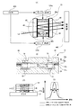
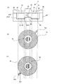
(分光測定器の全体構成例と光フィルターの構成例)
図1(A)および図1(B)は、分光測定器の全体構成例と光フィルターの構成例を示す図である。例えば、サンプル200の測色を行う場合には光フィルターへの入射光がサンプル200からの反射光となる光源100が用いられ、また、サンプル200の分光分析を行う場合には、例えば光フィルターへの入射光がサンプル200からの透過光となる光源100’が用いられる。なお、分光分析の対象となるサンプル200は、ガス(気体)の場合もあり得る。
(Example of overall configuration of spectrophotometer and example of optical filter)
FIG. 1A and FIG. 1B are diagrams showing an example of the overall configuration of a spectrometer and an example of the configuration of an optical filter. For example, when performing colorimetry on the
図1(A)に示されるように、分光測定器700は、光源100(あるいは100’)と、光源駆動部110と、複数の波長可変バンドパスフィルター(BPF(1)〜BPF(3))を備える光フィルター(分光部)300と、フォトダイオード等の受光素子PD(1)〜PD(3)を含む受光部400と、受光部400から得られる受光信号(電流信号)を電圧信号に変換し、その電圧値をデジタルデータ(分光スペクトルデータ)に変換する受光信号処理部500と、各部の動作を統括的に制御する制御部(例えば、マイクロコンピューターやゲートアレイ等で構成される)600と、分光スペクトルデータに基づいて、所与の信号処理(演算処理)を実行して分光光度分布等を求める信号処理部(演算部)650と、波長可変バンドパスフィルターBPF(1)〜BPF(3)の各々を駆動する光フィルター駆動部(単に駆動部という場合がある)120と、を有する。
As shown in FIG. 1A, the
光源100(100’)としては、例えば、白熱電球、蛍光灯、放電管、LED等の固体発光素子を用いた光源(固体発光素子光源)等を使用することができる。また、波長可変バンドパスフィルターBPF(1)〜BPF(3)の各々には、波長が異なる複数の分光帯域を設定することができる。光フィルター駆動部120から出力される駆動信号(例えば駆動電圧)のレベルに応じて、各フィルターBPF(1)〜BPF(3)の分光帯域の波長が適宜、決定される。
As the light source 100 (100 '), for example, a light source (solid light emitting element light source) using a solid light emitting element such as an incandescent bulb, a fluorescent lamp, a discharge tube, or an LED can be used. In addition, a plurality of spectral bands having different wavelengths can be set in each of the wavelength tunable bandpass filters BPF (1) to BPF (3). Depending on the level of the drive signal (for example, drive voltage) output from the optical
また、信号処理部650は、受光部400から得られる受光信号(分光スペクトルデータ)に基づいて各種演算を実行して、例えば、サンプル200に関する分光光度分布を求める。信号処理部650は、求められた分光光度分布情報Soutを出力する。分光光度分布の測定によって、例えば、サンプル200の測色や、サンプル200の成分分析等を行うことができる。
In addition, the
なお、光フィルター300および受光部400によって、光フィルターモジュール350が構成される。光フィルターモジュール350は、分光測定器に適用できる他、例えば、光通信装置の受信部(受光光学系と受光素子を含む)としても使用可能である。本実施形態における光フィルターモジュール350は、透過光の波長範囲を広くとることができ、また、分光スペクトルデータの取得を短時間で行えるという利点がある。
The
図1(B)に示すように、図1(A)の例における光フィルター300は、実質的に、波長400nm〜700nmの広範囲にわたる波長帯域(すなわち所望帯域)をカバーする、複数の分光帯域を設定可能な、波長可変フィルターである。すなわち、光フィルター300は、第1波長可変バンドパスフィルター(BPF(1))と、第2波長可変バンドパスフィルター(BPF(2))と、第3波長可変バンドパスフィルター(BPF(3))と、を有している。
As shown in FIG. 1 (B), the
第1波長可変バンドパスフィルター(BPF(1))は、例えば、波長400nm〜480nmの波長帯域(第1波長帯域)の光を分光し、かつ、帯域幅が20nmに設定されている5つの分光帯域(透過波長帯域)b1〜b5を有する。b1〜b5の各々の帯域の中心波長は、400nm,420nm,440nm,460nmおよび480nmである。第2波長可変バンドパスフィルター(BPF(2))は、500nm〜580nmの波長帯域(第2波長帯域)の光を分光し、帯域幅が20nmに設定されている5つの分光帯域(透過波長帯域)b6〜b10を有する。b6〜b10の各々の帯域の中心波長は、500nm,520nm,540nm,560nmおよび580nmである。第3波長可変バンドパスフィルター(BPF(3))は、波長600nm〜700nmの波長帯域(第3波長帯域)の光を分光し、帯域幅が20nmに設定されている6つの分光帯域(透過波長帯域)b11〜b16を有する。b11〜b16の各々の帯域の中心波長は、600nm,620nm,640nm,660nm,680nmおよび700nmである。また、図1(B)において、p1〜p16の各々は、光フィルター300が分光測定器に使用される場合における測定ポイントを示している。すなわち、16個の測定ポイントが設定されていることになる。
The first wavelength tunable bandpass filter (BPF (1)), for example, separates light in a wavelength band (first wavelength band) having a wavelength of 400 nm to 480 nm and has a bandwidth set to 20 nm. It has bands (transmission wavelength bands) b1 to b5. The center wavelengths of each band of b1 to b5 are 400 nm, 420 nm, 440 nm, 460 nm, and 480 nm. The second wavelength tunable bandpass filter (BPF (2)) splits light in the wavelength band (second wavelength band) of 500 nm to 580 nm, and has five spectral bands (transmission wavelength bands) whose bandwidth is set to 20 nm. ) B6 to b10. The center wavelengths of each band of b6 to b10 are 500 nm, 520 nm, 540 nm, 560 nm, and 580 nm. The third wavelength variable bandpass filter (BPF (3)) splits light in the wavelength band (third wavelength band) of wavelengths from 600 nm to 700 nm, and has six spectral bands (transmission wavelengths) whose bandwidth is set to 20 nm. Band) b11 to b16. The center wavelengths of each band of b11 to b16 are 600 nm, 620 nm, 640 nm, 660 nm, 680 nm, and 700 nm. In FIG. 1B, each of p1 to p16 indicates a measurement point when the
各波長可変バンドパスフィルターが分光する波長帯域は、原則的には、所望帯域を均等に分割した波長帯域とするのが好ましい。但し、図1(B)の例では、短波長側の波長帯域の光を分光するBPF(1)ならびに中波長の帯域の光を分光するBPF(2)に関して、5つの測定ポイント(p1〜p5,p6〜p10)が設定されているが、長波長側の帯域の光を分光するBPF(3)に関しては、偶数個の測定ポイントを確保するために、6つの測定ポイント(p11〜p16)が設定されている。長波長側の帯域において測定ポイント数を増やしているのは、光学膜の設計が容易である点を考慮したものである。例えば、各可変波長フィルターを可変ギャップエタロンで構成し、各フィルターに使用される光学膜の材料を共通化する場合を想定する。この場合、光の波長が長い方が、分光帯域の帯域幅を広く確保することが容易である。つまり、長波長域の方が、測定ポイントの数を増やすことが容易である。よって、各フィルターに関する測定ポイント数に差を設ける設計が必要となった場合には、長波長域を分光するフィルターについての測定ポイント数を増やすのが好ましい。 In principle, the wavelength band that each wavelength variable bandpass filter divides is preferably a wavelength band that is obtained by equally dividing the desired band. However, in the example of FIG. 1B, five measurement points (p1 to p5) are associated with BPF (1) that splits light in the short wavelength band and BPF (2) that splits light in the middle wavelength band. , P6 to p10) are set, but in order to secure an even number of measurement points for the BPF (3) that splits light in the long wavelength band, six measurement points (p11 to p16) are provided. Is set. The reason why the number of measurement points is increased in the long wavelength band is that the design of the optical film is easy. For example, it is assumed that each variable wavelength filter is composed of a variable gap etalon and the optical film material used for each filter is made common. In this case, the longer the wavelength of light, the easier it is to secure a wide spectral bandwidth. That is, it is easier to increase the number of measurement points in the long wavelength region. Therefore, when it is necessary to design a difference in the number of measurement points for each filter, it is preferable to increase the number of measurement points for the filter that divides the long wavelength region.
図1(A)および図1(B)に示される本実施形態における光フィルター300では、所望波長帯域(カバーすべき波長帯域)を一つの波長可変フィルターでカバーするのではなく、複数の(つまり2以上の)波長可変バンドパスフィルター(BPF(1)〜BPF(3))を用いてカバーし、かつ、各波長可変バンドパスフィルター(BPF(1)〜BPF(3))の各々を並行して駆動するという構成が採用される。
In the
すなわち、複数の波長可変バンドパスフィルター(少なくとも第1波長可変バンドパスフィルターBPF(1)および第2波長可変バンドパスフィルターBPF(2)を含む)の並行駆動によって、各フィルターの分光処理期間の少なくとも一部が時間軸上で重複し、したがって、所望波長帯域の全帯域を、所定帯域幅毎にスキャンするのに要する時間を短縮することができる。例えば、n個の波長可変バンドパスフィルターを同時に駆動する場合、所望波長帯域の全帯域をスキャンするのに要する時間は、例えば、従来の1/nに短縮される。よって、例えば、広い範囲の波長域を、効率的にカバー可能な光フィルターが実現される。 That is, by parallel driving of a plurality of wavelength tunable bandpass filters (including at least the first wavelength tunable bandpass filter BPF (1) and the second wavelength tunable bandpass filter BPF (2)), at least the spectral processing period of each filter. A part of them overlaps on the time axis, and therefore the time required to scan the entire band of the desired wavelength band for each predetermined bandwidth can be reduced. For example, when n wavelength tunable bandpass filters are driven simultaneously, the time required to scan the entire desired wavelength band is reduced to, for example, 1 / n of the conventional one. Therefore, for example, an optical filter capable of efficiently covering a wide wavelength range is realized.
また、複数の波長可変バンドパスフィルター(BPF(1)〜BPF(3))が、各々に割り当てられた波長帯域の光を分光することによって、個々の波長可変バンドパスフィルター(BPF(1)〜BPF(3))の可動部の可動範囲が抑制され、アクチュエーターの駆動電圧の上昇を抑制することができる。よって、光フィルター駆動部120を構築するのが容易となり、消費電力の削減も可能である。
A plurality of wavelength tunable bandpass filters (BPF (1) to BPF (3)) divides the light in the wavelength bands assigned to the respective wavelength tunable bandpass filters (BPF (1) to BPF (1) to The movable range of the movable part of BPF (3) is suppressed, and an increase in the drive voltage of the actuator can be suppressed. Therefore, it is easy to construct the optical
また、各波長可変バンドパスフィルター(BPF(1)〜BPF(3))を、例えば、可変ギャップエタロンフィルターで構成した場合に、各フィルターが分光すべき波長帯域を狭くできることから、各フィルターに使用される光学膜(例えば、屈折率の異なる膜を積層した構造をもち、光の反射特性と透過特性とを併せ持つ光学膜)の構成材料を共通化することができる。よって、光フィルター300の製造負荷を軽減することも可能となる。
In addition, when each wavelength tunable bandpass filter (BPF (1) to BPF (3)) is composed of, for example, a variable gap etalon filter, the wavelength band to be dispersed by each filter can be narrowed. The constituent material of the optical film (for example, an optical film having a structure in which films having different refractive indexes are stacked and having both light reflection characteristics and transmission characteristics) can be shared. Therefore, the manufacturing load of the
(可変ギャップエタロンフィルターの構成等)
図1(A)および図1(B)に示される波長可変バンドパスフィルター(BPF(1)〜BPF(3))の各々は、上述のとおり、例えば、可変ギャップエタロンフィルター(単に、可変ギャップエタロンという場合があり、また、単にフィルターという場合もある)によって構成することができる。可変ギャップエタロンのギャップを制御することによって、一つの光学フィルターを用いて、実質的に複数の(つまり2以上の)分光帯域を実現することが可能である。
(Configuration of variable gap etalon filter, etc.)
Each of the wavelength tunable bandpass filters (BPF (1) to BPF (3)) shown in FIGS. 1A and 1B is, for example, a variable gap etalon filter (simply a variable gap etalon). In some cases, the filter may be simply referred to as a filter). By controlling the gap of the variable gap etalon, it is possible to achieve substantially multiple (ie, two or more) spectral bands using a single optical filter.
図2(A)〜図2(D)は、可変ギャップエタロンフィルターの原理と構造例を示す図である。図2(A)に示すように、光フィルター300を構成する可変ギャップエタロンフィルター10は、互いに対向して配置される第1基板(例えば固定基板)20と、第2基板(例えば可動基板)30と、第1基板20の主面(表面)に設けられる第1光学膜40と、第2基板30の主面(表面)に設けられる第2光学膜50と、各基板によって挟持された、各基板間のギャップ(距離)を調整するためのアクチュエーター(例えば静電アクチュエーターや圧電素子等)80a,80bと、を有する。ギャップ値はG1に設定されている。
FIG. 2A to FIG. 2D are diagrams showing the principle and structure example of a variable gap etalon filter. As shown in FIG. 2A, the variable
なお、第1基板20および第2基板30の少なくとも一方が可動基板であればよく、双方を可動基板とすることも可能である。アクチュエーター80aおよびアクチュエーター80bは各々、光フィルター駆動部120a,120bの各々によって駆動される。また、各光フィルター駆動部120a,120bの動作は、制御部(制御回路)600によって制御される。
Note that at least one of the
所定角度θで外部から入射する光Linは、ほとんど散乱されることなく第1光学膜40を通過する。第1基板20に設けられた第1光学膜40と第2基板30に設けられた第2光学膜50との間で、光の反射が繰り返され、これによって、光の干渉が生じ、特定の条件を満たす波長の光のみが強められ、その強められた波長の光の一部は、第2基板30上の第2光学膜50を通過して、受光部400(受光素子)に到達する。干渉によってどの波長の光が強め合うかは、第1基板20と第2基板30との間のギャップに依存する。詳しくは、第1光学膜40と第2光学膜50との間のギャップに依存する。よって、ギャップを可変に制御することによって、通過する光の波長帯域を変化させることができる。
Light Lin incident from the outside at a predetermined angle θ passes through the first
図2(B)は、可変ギャップエタロンフィルターの断面構造の一例を示している。図2(B)に示されるように、可変ギャップエタロンフィルター10は、対向して平行に配置される第1基板20および第2基板30と、第1光学膜40および第2光学膜50と、第1基板20上において、第1光学膜40の周囲に形成されている第1電極60と、第2基板30上において、第2光学膜50の周囲に形成されている第2電極70と、を有する。第1電極60と第2電極70は、互いに対向して配置されており、この一対の電極によって、静電アクチュエーター80が形成される。静電アクチュエーター80を用いた可変ギャップエタロンの駆動の具体例については後述する。なお、ギャップ値(光学膜間の距離)はG1に設定されている。また、参照符号91a,91bは、酸化膜(SiO2膜)を示し、参照符号92a,92bは接合膜(例えばプラズマ重合膜)を示す。
FIG. 2B shows an example of a cross-sectional structure of the variable gap etalon filter. As shown in FIG. 2B, the variable
図2(C)は、第1基板20(例えばガラス基板)上に形成される第1光学膜40の構造例を示している。第1光学膜40は、一対(ワンペア)のシリコン酸化膜(SiO2膜(屈折率n=1.5))および酸化チタン膜(TiO2膜(屈折率n=2.5))を少なくとも有する積層膜である。但し、これに限定されるものではなく、Ag合金を用いた膜等であってもよい。
FIG. 2C shows a structure example of the first
第1光学膜40は、反射膜として機能し、また光透過膜としての機能を併せ持つ。酸化チタン膜(TiO2膜)の上には、保護膜としての酸化膜(SiO2膜)92が形成されている。この保護膜としての酸化膜92の厚みを調整することによって、ギャップを微調整することも可能である。なお、第2光学膜50も第1光学膜40と同様の構成とすることができる。
The first
図2(D)は、積層する光学膜のペア数に依存して、バンドパスフィルターの光透過特性がどのように変化するかを示している(但し、一例である)。単層膜(ワンペアの膜)の場合は、例えば実線で示すようなバンドパスフィルター特性(透過率の半値幅w1)となり、多層膜(2ペア以上の膜)の場合は、例えば点線で示すようなバンドパスフィルター特性(透過率の半値幅w2(w2>w1)となる。このように、光学膜を構成するペア数を増加させることによって、バンドパスフィルターの半値幅(つまり光透過帯域の帯域幅)を広げることができる。 FIG. 2D shows how the light transmission characteristics of the bandpass filter change depending on the number of pairs of optical films to be stacked (however, it is an example). In the case of a single layer film (one pair of films), for example, the bandpass filter characteristics (transmittance half-value width w1) as shown by a solid line, and in the case of a multilayer film (two pairs or more films), for example, as shown by a dotted line Bandpass filter characteristics (transmittance half width w2 (w2> w1). In this way, by increasing the number of pairs constituting the optical film, the band width of the bandpass filter (that is, the band of the light transmission band) (Width) can be widened.
例えば、短波長の分光帯域の光を分光する可変ギャップエタロンをBPF(1)とし、中波長の分光帯域の光を分光する可変ギャップエタロンをBPF(2)とし、長波長の分光帯域を分光する可変ギャップエタロンをBPF(3)とし、各エタロンの初期ギャップ値を1μmとしたとき、BPF(1)における第1光学膜40および第2光学膜50の積層ペア数は1とすることができ、BPF(2)における第1光学膜40の積層ペア数は1、第2光学膜50の積層ペア数は2とすることができ、BPF(3)における第1光学膜40の積層ペア数は1、第2光学膜50の積層ペア数は2とすることができる。可変ギャップエタロンの駆動方法としては、後述するように、第1駆動方法(各フィルターの初期ギャップ値が同じ)と、第2駆動方法(各フィルターの初期ギャップ値が異なる)とがあるが、いずれの駆動方法においても、上記の光学膜のペア数で対応可能である。但し、上記の例は一例であり、これに限定されるものではない。
For example, a variable gap etalon that splits light in a short wavelength spectral band is BPF (1), a variable gap etalon that splits light in a medium wavelength spectral band is BPF (2), and a long wavelength spectral band is split. When the variable gap etalon is BPF (3) and the initial gap value of each etalon is 1 μm, the number of stacked pairs of the first
(分光測定装置の具体例について)
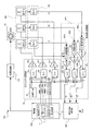
次に、分光測定器700の、より具体的な構成例について説明する。図3は、分光測定装置の具体的な構成例を示す図である。なお、図3において、前掲の図面と共通する部分には同じ参照符号が付されている。
(Specific examples of spectrometers)
Next, a more specific configuration example of the
図3の分光測定装置では、複数の可変ギャップエタロンフィルターを並行して駆動すると共に、各フィルターを経由した光を受光部によって受光して得られる受光信号の処理も、並行して実行する。この構成を採用することによって、光の分光処理が並列化され、さらに受光信号の信号処理も並列化される。よって、分光測定器700の測定効率が格段に向上する。したがって、例えば、簡素化された構成を備え、小型軽量で、広い波長範囲をカバー可能であり、かつ、測定時間を格段に短縮可能な、使い勝手のよい分光測定器を実現することができる。
In the spectroscopic measurement apparatus of FIG. 3, a plurality of variable gap etalon filters are driven in parallel, and processing of received light signals obtained by receiving light passing through the filters by a light receiving unit is also executed in parallel. By adopting this configuration, the light spectral processing is parallelized, and the signal processing of the received light signal is also parallelized. Therefore, the measurement efficiency of the
制御部600は、同期クロック生成回路15と、電圧設定メモリー17と、を有する。電圧設定メモリー17には、電圧データテーブル19が記憶されている。電圧データテーブル19の電圧データに基づいて、可変ギャップエタロンフィルターの駆動電圧のレベルが決定される。
The
光フィルター駆動部120は、基準電圧源23と、D/A変換器33a〜33cと、アンプ42a〜42cと、を有する。基準電圧源23は、電圧レベルが異なる、複数の駆動電圧Vref(1)〜Vref(m)を並列に出力する。ここで、mは2以上の整数である。例えば、D/A変換器33aには、複数の駆動電圧(Vref(1)〜Vref(m))と、電圧データD1とが入力される。D/A変換器33aは、複数の駆動電圧(Vref(1)〜Vref(m))の中から、電圧データD1に対応する駆動電圧を選択して出力する。駆動電圧はアンプ42aで増幅され、増幅された駆動電圧は、光フィルター300に含まれる第1波長可変フィルターとしての第1可変ギャップエタロンフィルターBPF(1)に供給される。この駆動電圧によって、第1可変ギャップエタロンフィルターBPF(1)のギャップが制御され、透過光の波長帯域(つまり分光帯域)が決定される。
The optical
同様に、D/A変換器33bには、複数の駆動電圧(Vref(1)〜Vref(m))と、電圧データD2とが入力される。D/A変換器33bから出力される駆動電圧は、
アンプ42bで増幅され、増幅された駆動電圧は、第2可変ギャップエタロンフィルターBPF(2)に供給される。この駆動電圧によって、第2可変ギャップエタロンフィルターBPF(2)のギャップが制御され、透過光の波長帯域(分光帯域)が決定される。
Similarly, a plurality of drive voltages (Vref (1) to Vref (m)) and voltage data D2 are input to the D /
The drive voltage amplified by the
同様に、D/A変換器33cには、複数の駆動電圧(Vref(1)〜Vref(m))と、電圧データD3とが入力される。D/A変換器33cから出力される駆動電圧は、
アンプ42cで増幅され、増幅された駆動電圧は、第3可変ギャップエタロンフィルターBPF(3)に供給される。この駆動電圧によって、第3可変ギャップエタロンフィルターBPF(3)のギャップが制御され、透過光の波長帯域(分光帯域)が決定される。
Similarly, a plurality of drive voltages (Vref (1) to Vref (m)) and voltage data D3 are input to the D /
The drive voltage amplified by the
D/A変換器33a〜33cの各々は、制御部600に含まれる同期クロック生成回路15から出力される同期クロックCLK1に同期して、例えば同時に動作する。各フィルターを同時に駆動すると、測定時間を最も短くすることができる。但し、必ずしも同時である必要はなく、例えば、各フィルターの駆動に関して、若干のタイミング差が存在していてもよい。
Each of the D /
D/A変換器33a〜33cの各々が共通のクロック(同期クロックCLK1)に基づいて並行して動作することによって、BPF(1)〜BPF(3)の各々の分光帯域が実現される期間の少なくとも一部が、時間軸上で重複することになり、したがって、分光処理に要する時間が短縮され、効率的な分光処理が実現される。例えば、第1回目の測定期間において、BPF(1)に第1分光帯域が実現され、BPF(2)に第2分光帯域が実現され、BPF(3)に第3分光帯域が実現されるとすると、第1分光帯域が実現される期間と、第2分光帯域あるいは第3分光帯域が実現される期間の少なくとも一部が、時間軸上で重複することになる。また、次の測定期間において、BPF(1)に第4分光帯域が実現され、BPF(2)に第5分光帯域が実現され、BPF(3)に第6分光帯域が実現されるとすると、第4分光帯域が実現される期間と、第5分光帯域あるいは第6分光帯域が実現される期間の少なくとも一部が、時間軸上で重複することになる。したがって、所望波長帯域の全帯域を、所定帯域幅毎にスキャンするのに要する時間を短縮することができる。図3の例では、3個の可変ギャップエタロンが使用されており、これらを同時に駆動した場合には、所望波長帯域の全帯域をスキャンするのに要する時間は、従来の1/3に短縮される。よって、例えば、広い範囲の波長域を効率的にカバー可能な光フィルターが実現される。
The D /
また、複数の波長可変バンドパスフィルターが、各々に割り当てられた波長帯域を分光することによって、個々の波長可変バンドパスフィルターの可動部の可動範囲が抑制され、アクチュエーターの駆動電圧の上昇を抑制することができる。よって、光フィルター駆動部120を構築するのが容易となり、消費電力の削減も可能である。また、各可変ギャップエタロンBPF(1)〜BPF(3)の各々に使用される光学膜(例えば、屈折率の異なる膜を積層した構造をもち、光の反射特性と透過特性とを併せ持つ光学膜)を共通化することができる。このことは、光フィルター300の構成の簡素化に役立つ。
In addition, a plurality of wavelength tunable bandpass filters divide the wavelength band assigned to each, thereby suppressing the movable range of the movable part of each wavelength tunable bandpass filter and suppressing an increase in the drive voltage of the actuator. be able to. Therefore, it is easy to construct the optical
受光部400に含まれる第1受光素子PD(1)は、BPF(1)を経由した(通過した)光を受光し、光電変換によって第1受光信号(電流信号)S1を生成し、出力する。同様に、第2受光素子PD(2)は、BPF(2)を経由した光を受光し、光電変換によって第2受光信号(電流信号)S2を生成し、出力する。第3受光素子PD(3)は、BPF(3)を経由した光を受光し、光電変換によって第3受光信号(電流信号)S3を生成し、出力する。
The first light receiving element PD (1) included in the
受光信号処理部500は、3つの信号処理経路502a〜502cを備える。第1信号処理経路502aには、電流/電圧変換を行うI−V変換回路72aと、アンプ82aと、A/D変換器93aと、が設けられる。同様に、第2信号処理経路502bには、電流/電圧変換を行うI−V変換回路72bと、アンプ82bと、A/D変換器93b、が設けられる。第3信号処理経路502cには、電流/電圧変換を行うI−V変換回路72cと、アンプ82cと、A/D変換器93cと、が設けられる。
The received light
A/D変換器93a〜93cの各々は、例えば、同期クロックCLK2に基づいて同時に動作する。但し、これは一例である。BPF(1)〜BPF(3)の各々の駆動に関してタイミング差が設けられているときは、そのタイミング差に応じて、各A/D変換器93a〜93cの動作タイミングにも差が設けられる。
Each of the A /
各A/D変換器93a〜93cの各々からは、第1受光データS1’〜第3受光データS3’の各々が出力される。第1受光データS1’〜第3受光データS3’の各々は、信号処理部(演算部)650に供給される。
Each of the A /
信号処理部(演算部)650は、第1受光データS1’〜第3受光データS3’の各々に基づいて、所定の信号処理を実行し、例えば、サンプル200(図1参照)の分光光度分布を測定する。信号処理部650は、分光光度分布情報Soutを出力する。分光光度分布の測定によって、例えば、サンプル200の測色、あるいはサンプル200の成分分析等を行うことができる。なお、光源100は、信号処理部650の準備が整うまでの期間において、無駄な電力消費を防止するために消灯しておくことができる。但し、複数のサンプルに関して、連続的に測定を実行する場合には、光源100の駆動状態を継続してもよい。
The signal processing unit (calculation unit) 650 performs predetermined signal processing based on each of the first light reception data S1 ′ to the third light reception data S3 ′, for example, the spectrophotometric distribution of the sample 200 (see FIG. 1). Measure. The
図3の分光測定器700では、光フィルターを構成する3つの可変ギャップエタロンBPF(1)〜BPF(3)の各々の駆動が並列的に行われ、また、各フィルターを経由した光を受光部400が受光して得られる受光信号の処理も並列的に行われる。受光信号の取得ならびに受光信号の処理の双方が並列化されていることから、効率的な分光測定が実現される。よって、分光測定の開始から終了までの時間を、従来例に比べて、大幅に短縮することができる。
In the
図4(A)および図4(B)は、制御部に含まれる同期クロック生成回路の構成と動作の一例を示す図である。図4(A)に示されるように、同期クロック生成回路15は、クロック生成器810と、遅延回路820と、を有している。クロック生成器810には、クロックの生成開始/終了を指示するスタート/ストップ信号STと、基準クロックCK(システムクロック等)CKと、が入力される。
4A and 4B are diagrams illustrating an example of the configuration and operation of the synchronous clock generation circuit included in the control unit. As shown in FIG. 4A, the synchronous
同期クロック生成回路15は、クロックの生成が停止している状態において、スタート/ストップ信号STが入力されると、同期クロックCLK1の生成を開始する。また、クロックが生成されている期間において、スタート/ストップ信号STが入力されると、同期クロックCLK1の生成を終了する。遅延回路820は、同期クロックCLK1を所定時間だけ遅延させる。この結果として、遅延回路820から、同期クロックCLK2が出力される。
When the generation of the clock is stopped, the synchronous
図4(B)の例では、時刻t1にスタート/ストップ信号STが入力され、時刻t1に同期クロックCLK1の生成が開始され、時刻t2に同期クロックCLK2の生成が開始される。また、時刻t4にスタート/ストップ信号STが入力され、時刻t5以降、同期クロックCLK1が停止され、また、時刻t6以降、同期クロックCLK2が停止される。 In the example of FIG. 4B, the start / stop signal ST is input at time t1, generation of the synchronous clock CLK1 is started at time t1, and generation of the synchronous clock CLK2 is started at time t2. In addition, the start / stop signal ST is input at time t4, the synchronous clock CLK1 is stopped after time t5, and the synchronous clock CLK2 is stopped after time t6.
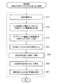
図5は、図3に示される分光測定装置の動作手順例を示すフロー図である。上述のとおり、3つの可変ギャップエタロン(BPF(1)〜BPF(3))の各々を用いた分光測定処理が、並行して実行される。 FIG. 5 is a flowchart showing an example of an operation procedure of the spectroscopic measurement apparatus shown in FIG. As described above, the spectroscopic measurement process using each of the three variable gap etalons (BPF (1) to BPF (3)) is executed in parallel.
分光測定処理は、例えば、ステップST1〜ステップST7を含む。すなわち、光源が駆動され(ステップST1)、D/A変換器33a〜33cの各々に、分光帯域の波長に応じた電圧データが入力され、D/A変換器33a〜33cの各々から、可変ギャップエタロンBPF(1)〜BPF(3)の各々用の駆動電圧が出力される(ステップST2)。次に、アンプ42a〜42cによって、駆動電圧が増幅され、増幅された駆動電圧が、可変ギャップエタロンBPF(1)〜BPF(3)の各々に印加される(ステップST3)。
The spectroscopic measurement process includes, for example, steps ST1 to ST7. That is, the light source is driven (step ST1), voltage data corresponding to the wavelength of the spectral band is input to each of the D /
次に、受光素子PD(1)〜PD(3)の各々から、受光信号(電流信号)S1〜S3の各々が出力される(ステップST4)。受光信号S1〜S3の各々は、I−V変換回路72a〜72cの各々によって電圧信号に変換され、さらに、アンプ82a〜82cの各々によって増幅される(ステップST5)。次に、A/D変換器93a〜93cの各々によって、A/D変換が実行される(ステップST6)。信号処理部650は、所定の演算を実行し、この結果として、分光光度分布情報が取得される(ステップST7)。
Next, each of the light receiving signals (current signals) S1 to S3 is output from each of the light receiving elements PD (1) to PD (3) (step ST4). Each of the received light signals S1 to S3 is converted into a voltage signal by each of the
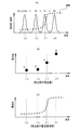
図6(A)〜図6(C)は、分光測定によって、サンプルの物体色を測定する方法の一例を示す図である。ここでは、説明の便宜上、測定ポイント数を4としている。図6(A)では、可変ギャップエタロンに入射するサンプルの分光強度分布が破線で示されている。図6(A)において、ギャップ値がG1であるとき、可変ギャップエタロンは、波長λ1を中心波長とした透過特性を有している。ギャップ値がG0,G1,G2,G3の順に変化すると、透過帯域の中心波長は、λ0、λ1、λ2,λ3の順に変化する。 6A to 6C are diagrams illustrating an example of a method for measuring the object color of a sample by spectroscopic measurement. Here, for convenience of explanation, the number of measurement points is four. In FIG. 6A, the spectral intensity distribution of the sample incident on the variable gap etalon is indicated by a broken line. In FIG. 6A, when the gap value is G1, the variable gap etalon has transmission characteristics with the wavelength λ1 as the center wavelength. When the gap value changes in the order of G0, G1, G2, and G3, the center wavelength of the transmission band changes in the order of λ0, λ1, λ2, and λ3.
受光部400からは、図6(B)に示されるような、受光光量に応じた電流I3〜I0の各々が出力される。各フィルターの中心波長λと、電流の電流値との関係を求めることによって、図6(C)に示されるような分光特性を示す特性線(分光光度分布曲線)を描くことができる。 Each of the currents I3 to I0 corresponding to the amount of received light as shown in FIG. By obtaining the relationship between the center wavelength λ of each filter and the current value of the current, a characteristic line (spectrophotometric distribution curve) showing spectral characteristics as shown in FIG. 6C can be drawn.
(可変ギャップエタロンの具体的構造ならびに具体的動作について)
以下、可変ギャップエタロンの具体的な構造例ならびに具体的な動作例について説明する。図7(A)および図7(B)は、可変ギャップエタロンの具体的な構造例と、その動作を説明するための図である。
(Specific structure and operation of variable gap etalon)
Hereinafter, a specific structural example and a specific operation example of the variable gap etalon will be described. FIG. 7A and FIG. 7B are diagrams for explaining a specific structure example of the variable gap etalon and its operation.
図7(A)において、第1基板20と例えば一体で、第2基板30を可動に支持する支持部22が形成されている。支持部22は、第2基板30に設けてもよく、あるいは第1,第2基板20,30とは別体で形成してもよい。
In FIG. 7A, a
第1,第2基板20,30は、それぞれ例えば、ソーダガラス、結晶性ガラス、石英ガラス、鉛ガラス、カリウムガラス、ホウケイ酸ガラス、無アルカリガラスなどの各種ガラスや、水晶などにより形成することができる。これらの中でも、各基板20,30の構成材料としては、例えばナトリウム(Na)やカリウム(K)などのアルカリ金属を含有したガラスが好ましく、このようなガラスにより各基板20,30を形成することで、光学膜(反射膜)40,50や、各電極60,70の密着性や、基板同士の接合強度を向上させることが可能となる。そして、これらの2つの基板20,30は、例えばプラズマ重合膜を用いた表面活性化接合などにより接合されることで、一体化されている。第1,第2基板20,30の各々は、一辺が例えば10mmの正方形に形成され、ダイヤフラムとして機能する部分の最大直径は例えば5mmである。
The first and
第1基板20は、例えば、厚みが500μmに形成されるガラス基材をエッチングにより加工することで形成される。第1基板20は、第2基板30と対向する対向面のうちの中央の第1対向面20A1に、例えば円形の第1光学膜40が形成されている。同様に、第2基板30は、厚みが例えば200μmに形成されるガラス基材をエッチングにより加工することで形成される。第2基板30は、第1基板20と対向する対向面30Aの中央位置に、第1光学膜40と対向する例えば円形の第2光学膜50が形成されている。
The
なお、第1,第2光学膜40,50は、例えば直径が約3mmの円形状に形成されている。この第1,第2光学膜40,50は、例えば、透過率の半値幅も狭く分解能が良好な、例えばTiO2とSiO2との積層膜からなる誘電体多層膜を使用することができ、また、AgC層等によって構成することもできる。第1,第2光学膜40,50は、例えば、スパッタリングなどの手法により第1,第2基板20,30に形成することができる。光学膜の膜厚寸法は、例えば0.03μmに形成されている。本実施形態では、第1,第2光学膜40,50として、可視光全域を分光できる光学膜を用いる。
The first and second
さらに、第1,第2基板20,30の各対向面20A1,20A2,30Aとは逆側の面にて、第1,第2光学膜40,50に対応する位置に図示しない反射防止膜(AR)を形成することができる。この反射防止膜は、低屈折率膜および高屈折率膜を交互に積層することで形成され、第1,第2基板20,30の界面での可視光の反射率を低下させ、透過率を増大させる。
Further, an antireflection film (not shown) is provided at a position corresponding to the first and second
これら第1,第2光学膜40,50は、図7(A)に示す電圧非印加状態にて初期ギャップ値G10を介して対向配置されている。なお、ここでは第1光学膜40を固定鏡とし、第2光学膜50を可動鏡とするが、上述した第1,第2基板20,30の態様に応じて、第1,第2光学膜40,50のいずれか一方又は双方を可動とすることができる。
These first and second
平面視で第1光学膜40の周囲の位置であって、第1基板20の第1対向面20A1の周囲の第2対向面20A2には、例えば下部電極(第1電極)60が形成されている。同様に、第2基板30の対向面30Aには、下部電極60と対向して上部電極(第2電極)70が設けられている。下部電極(第1電極)60と上部電極(第2電極)70は、ギャップ値G5を介して、対向配置されている。なお、下部電極60および上部電極70の表面は、絶縁膜にて被覆することができる。また、平面視とは各基板の基板厚み方向から見た場合をいう。
For example, a lower electrode (first electrode) 60 is formed on the second opposing surface 20A2 around the first opposing surface 20A1 of the
本実施形態では、第1基板20が第2基板30と対向する面は、第1光学膜40が形成される第1対向面20A1と、平面視で第1対向面20A1の周囲に配置されて、下部電極60が形成される第2対向面20A2とを有する。第1対向面20A1と第2対向面20A2とは同一面であってもよいが、本実施形態では第1対向面20A1と第2対向面20A2との間には段差があり、第1対向面20A1の方が第2対向面20A2よりも第2基板30に近い位置に設定している。これにより、初期ギャップ値G10<ギャップ値G5の関係が成立する。
In the present embodiment, the surface of the
また、光フィルター300では、平面視で第2光学膜50の周囲に配置された上部電極70に共通電圧(例えば接地電圧)を印加し、平面視で第1光学膜40の周囲に配置された下部電極60に電圧を印加することによって、図7(B)に示すように、対向電極間に矢印で示す静電力(個々では静電引力)F1を生じさせることができる。すなわち、下部電極60および上部電極70によって静電アクチュエーター80が構成される。この静電引力F1によって、第1,第2光学膜40,50間のギャップを初期ギャップ値G10の大きさよりも小さいギャップとなるように可変に制御することができる。光学膜間のギャップの大きさによって透過光の波長が決まる。よって、ギャップを変化させることで透過波長を選択することが可能となる。
In the
図7(B)に示すように、入射光は、例えば第2基板30の上方から入射する。可変ギャップエタロンのギャップ値によって決まる波長帯域(分光帯域)の光のみが第1基板20を通過して出力光となる。その出力光は、受光部400によって受光され、受光強度に応じた電気信号(受光信号)が得られる。
As shown in FIG. 7B, the incident light enters from above the
図7(A)および図7(B)に示す例では、可動基板である第2基板30の撓み性を確保するために、図1に示すように、上部電極(第2電極)70が形成される領域を例えば厚み寸法が50μm程度の薄肉部34としている。この薄肉部34は、第2光学膜50が配置される領域の厚肉部32、および支持部22と接触する領域の厚肉部36よりも肉薄に形成されている。換言すれば、第2基板30は、第2光学膜50及び上部電極70が形成される面30Aは平坦面であり、第2光学膜50が配置される第1領域に厚肉部32が形成され、上部電極70が形成される第2領域に薄肉部34が形成される。こうして、薄肉部34にて撓み性を確保しながら、厚肉部32を撓み難くすることで、第2光学膜50は平面度を保ってギャップを可変することが可能となる。
In the example shown in FIGS. 7A and 7B, an upper electrode (second electrode) 70 is formed as shown in FIG. 1 to ensure the flexibility of the
図8(A)〜図8(C)は、可変ギャップエタロンフィルターにおける、電極および光学膜の配置を説明するための図である。図8(A)は可変ギャップエタロンフィルターの断面図であり(参照符号は前掲の図面と同じである)、図8(B)は、上部電極(第2電極)70および第2光学膜50の平面視における配置を示す図であり、図8(C)は、下部電極(第1電極)60および第1光学膜40の平面視における配置を示す図である。
FIG. 8A to FIG. 8C are diagrams for explaining the arrangement of electrodes and optical films in the variable gap etalon filter. FIG. 8A is a cross-sectional view of a variable gap etalon filter (reference numerals are the same as those in the above-mentioned drawings), and FIG. 8B shows the upper electrode (second electrode) 70 and the second
図8(A)〜図8(C)に示されるように、第1基板20の中央部に第1光学膜40が設けられ、第2基板30の中央部において、第1光学膜40に対向するように第2光学膜50が設けられており、また、第1電極(第1駆動電極)60は、第1基板20に設けられ、平面視において、第1光学膜40の周囲に(具体的には、第1光学膜40を取り囲むように)形成されており、第2電極(第2駆動電極)70は、第2基板30に設けられ、平面視において、第2光学膜50の周囲に(具体的には、第2光学膜50を取り囲むように)形成されている。なお、図8(A)および図8(B)において、参照符号70Aおよび60Aは各々、引き出し電極を示す。
As shown in FIGS. 8A to 8C, the first
このような構造をもつ光フィルター300は、光学膜(第1光学膜40および第2光学膜50)が形成される領域と、電極(下部電極60および上部電極70)が形成される領域とは、平面視で異なる領域となり(図8(B)および図8(C)参照)、よって、特許文献1に記載される例のように光学膜と電極とが積層されることはない。よって、第1,第2基板20,30の少なくとも一方(本実施形態では第2基板30)が可動基板とされても、光学膜と電極が積層されないために可動基板は撓み易さを確保できる。しかも、特許文献1に記載される光フィルターとは異なり、下部電極60および上部電極70上には光学膜が形成されないので、透過型または反射型波長可変干渉フィルターとして光フィルター300を利用しても、下部、上部電極60,70を、透明電極とする制約も生じない。なお、下部、上部電極60,70を仮に透明電極としたとしても、透過特性には影響が及ぶ。これに対して、図8の例では、下部電極60および上部電極70上には光学膜が形成されず、電極部分は光が通過しない領域となる。よって、透過型波長可変干渉フィルターである光フィルター300において、所望の透過特性を確保することが容易である。
The
図9は、静電アクチュエーターを用いたギャップ制御について説明するための図である。図9に示される光フィルター駆動部120には、D/A変換器33が設けられている。先に説明したように、D/A変換器33からは、電圧データDに対応した駆動電圧が出力される。その駆動電圧は、例えば、静電アクチュエーターを構成する上部電極(第2電極)70に印加される。一方、下部電極(第1電極)60の電位は固定されている(例えば接地されている)。上部電極(第2電極)70と下部電極(第1電極)60の間に電位差ΔVsegが生じると、これに伴って静電引力が発生し、可動基板である第2基板30が撓み、第1光学膜40と第2光学膜50との間のギャップが変化する(つまり、ギャップが縮小される)。
FIG. 9 is a diagram for explaining gap control using an electrostatic actuator. The optical
(第2実施形態)
本実施形態では、可変ギャップエタロンフィルターの具体的な駆動方法について説明する。可変ギャップエタロンフィルターの駆動方法としては、各フィルターの初期ギャップ値を同じ値に設定しておき、各フィルターに印加する駆動電圧のレベルを異ならせる方法(第1の駆動方法)と、各フィルターの初期ギャップ値を異なる値に設定しておき、各フィルターに印加する駆動電圧のレベルを同じとする方法(第2の駆動方法)とがある。以下、順に説明する。
(Second Embodiment)
In the present embodiment, a specific driving method of the variable gap etalon filter will be described. As the driving method of the variable gap etalon filter, the initial gap value of each filter is set to the same value, and the level of the driving voltage applied to each filter (first driving method) is different. There is a method (second driving method) in which the initial gap value is set to a different value and the level of the driving voltage applied to each filter is the same. Hereinafter, it demonstrates in order.
(第1の駆動方法)
図10は、可変ギャップエタロンフィルターの第1の駆動方法を説明するための図である。図10の上側に示されるように、3つの可変ギャップエタロンフィルター10A,10B,10Cが並置されている。
(First driving method)
FIG. 10 is a diagram for explaining a first driving method of the variable gap etalon filter. As shown in the upper side of FIG. 10, three variable
各フィルター10A,10B,10Cの初期ギャップ値は、共にG10に設定されている。また、各フィルター10A,10B,10Cは、図1(A)に示される、波長可変バンドパスフィルターBPF(1)〜BPF(3)の各々に相当する。各フィルター10A,10B,10Cは、先に図7を用いて説明した構造を有している。ここでは、可変ギャップエタロンフィルター10Aは、短波長側の分光帯域を分光し、可変ギャップエタロンフィルター10Bは、中波長の分光帯域を分光し、可変ギャップエタロンフィルター10Cは、長波長側の分光帯域を分光するものとする。
The initial gap values of the
各フィルター10A,10B,10Cは、例えば、同時に駆動される。図10の下側に記載されるように、可変ギャップエタロンフィルター10Aの駆動が開始されると、その直後に駆動電圧のレベルは第1レベルVAまで上昇し、以降、段階的に電圧レベルが上昇する。同様に、可変ギャップエタロンフィルター10Bの駆動が開始されると、その直後に駆動電圧のレベルは第2レベルVBまで上昇し、以降、段階的に電圧レベルが上昇する。
Each
可変ギャップエタロンフィルター10Cの駆動が開始されると、その直後に駆動電圧のレベルは第3レベルVCまで上昇し、以降、段階的に電圧レベルが上昇する。これに伴い、各フィルター10A,10B,10Cにおけるギャップが個別に制御され、各フィルター10A,10B,10Cのギャップ値は異なる値となり、各フィルター10A,10B,10Cにおいて、所望波長の分光帯域が実現される。
When the drive of the variable
このような第1の駆動方法を採用した場合には、各フィルター10A,10B,10Cに、レベルが異なる駆動電圧を印加することができる。よって、仮に各フィルターの特性がばらついたとしても、例えば、そのばらつきを補償するように駆動電圧を調整する(微調整する)ことができる。各フィルター10A,10B,10Cに最適な駆動電圧が印加されるため、各フィルター10A,10B,10Cの分光帯域の精度が向上する。
When such a first driving method is employed, driving voltages having different levels can be applied to the
また、各フィルター10A,10B,10Cの駆動電圧が異なるため、電圧印加時に生じるオーバーシュート(ならびにアンダーシュート)の周期に差が生じる。各駆動電圧の揺れが重畳されると、大きなノイズが生じて、例えば、光フィルター駆動部120における基準電位(グランドGNDや電源電位VDD)に大きな変動が生じる場合がある。しかし、第1の駆動方法を採用した場合には、各駆動電圧の揺れの周期が異なることからノイズが分散され、よって、大きなノイズが生じにくくなる。また、フィルター毎に、駆動電圧を調整することができるため、例えば、駆動電圧のレベルを切り換える場合における、1回の切り換え当たりの電圧の変化量を、小さく抑制するといった微調整も行い易くなる。この場合、電圧切り換え時における、駆動電圧のオーバーシュートを抑制することができる。
In addition, since the drive voltages of the
(第2の駆動方法)
図11は、可変ギャップエタロンフィルターの第2の駆動方法を説明するための図である。図11の上側に示されるように、3つの可変ギャップエタロンフィルター10A,10B,10Cが並置されている。各フィルター10A,10B,10Cは、図1(A)に示される、波長可変バンドパスフィルターBPF(1)〜BPF(3)の各々に相当する。フィルター10Aの初期ギャップ値はG10に設定され、フィルター10Bの初期ギャップ値はG20に設定され、フィルター10Cの初期ギャップ値はG30に設定されている。
(Second driving method)
FIG. 11 is a diagram for explaining a second driving method of the variable gap etalon filter. As shown in the upper side of FIG. 11, three variable
フィルター10A,10B,10Cは、先に図7を用いて説明した構造を有しており、また、図10の例と同様に、可変ギャップエタロンフィルター10Aは、短波長側の分光帯域を分光し、可変ギャップエタロンフィルター10Bは、中波長の分光帯域を分光し、可変ギャップエタロンフィルター10Cは、長波長側の分光帯域を分光するものとする。
The
上述のとおり、各フィルター10A,10B,10Cの初期ギャップ値は異なる値に設定されている。つまり、各フィルター10A,10B,10Cが分光する分光帯域の、一端側の波長に対応するギャップ値が選択されている。各フィルター10A,10B,10Cは、例えば、同時に駆動される。図10の下側に記載されるように、可変ギャップエタロンフィルター10A,10B,10Cの駆動が開始されると、各フィルター10A,10B,10Cには、共通の駆動電圧が供給される。駆動電圧のレベルは、所定期間毎に段階的に上昇する。
As described above, the initial gap values of the
第2の駆動方法によれば、各フィルター10A,10B,10Cの駆動電圧を共通化することができる。よって、制御部600に設けられる、電圧設定メモリー17の電圧データテーブル19(図3参照)に設定される駆動電圧値の数が減少する。n個の可変ギャップエタロンフィルターを使用する場合、設定電圧数は1/nでよいことになる。したがって、電圧設定メモリー17のメモリー領域が少なくて済む。メモリー容量を低減できることから、電圧設定メモリー17の専有面積が減少し、小型化に有利となり、また、例えば、電圧設定メモリー17として、低コストのROM等を使用することもできる。
According to the second driving method, the driving voltages of the
また、駆動電圧のレベルを切り換える場合における、1回の切り換え当たりの電圧変化量がそれほど大きくなければ、駆動電圧切り換え時におけるノイズは、それほど問題とはならない。また、可変ギャップエタロンの構造として、先に図7(A)および図7(B)を用いて説明したデバイス構造を採用すると、正確かつ安定したギャップ制御が実現することから、各フィルター10A,10B,10Cの特性のばらつきを、極力抑制することができる。よって、各フィルターに同じ駆動電圧を印加する場合でも、各フィルター10A,10B,10Cにおけるギャップ制御の精度は確保される。
Further, if the amount of voltage change per switching when switching the driving voltage level is not so large, the noise at the switching of the driving voltage is not so problematic. Further, if the device structure described above with reference to FIGS. 7A and 7B is employed as the structure of the variable gap etalon, accurate and stable gap control is realized, so that each
図12(A)および図12(B)は、測定波長に対する、具体的な駆動電圧値の例を示す図である。図12(A)は、上記の第1の駆動方法を採用する場合の例を示し、図12(B)は、上記の第2の駆動方法を採用する場合の例を示す。 12A and 12B are diagrams illustrating examples of specific drive voltage values with respect to the measurement wavelength. FIG. 12A shows an example in which the above first driving method is adopted, and FIG. 12B shows an example in which the above second driving method is adopted.
図12(A),図12(B)の各例では、測定波長(分光帯域の中心波長)が400nm〜480(短波長帯域)において、測定ポイントp1〜p5が設けられており、測定波長(分光帯域の中心波長)が500nm〜580(中波長帯域)において、測定ポイントp6〜p10が設けられており、測定波長(分光帯域の中心波長)が600nm〜780(短波長帯域)において、測定ポイントp11〜p16が設けられている。 In each example of FIGS. 12A and 12B, measurement points p1 to p5 are provided at a measurement wavelength (center wavelength of a spectral band) of 400 nm to 480 (short wavelength band), and the measurement wavelength ( Measurement points p6 to p10 are provided when the center wavelength of the spectral band is 500 nm to 580 (medium wavelength band), and measurement points are provided when the measurement wavelength (center wavelength of the spectral band) is 600 nm to 780 (short wavelength band). p11 to p16 are provided.
図12(A)に示される駆動電圧41Vが、図10の例における第1電圧レベルVAに相当し、駆動電圧36Vが、図10の例における第2電圧レベルVBに相当し、駆動電圧24Vが、図10の例における第3電圧レベルVCに相当する。 The drive voltage 41V shown in FIG. 12A corresponds to the first voltage level VA in the example of FIG. 10, the drive voltage 36V corresponds to the second voltage level VB in the example of FIG. 10, and the drive voltage 24V is This corresponds to the third voltage level VC in the example of FIG.
図12(A)の例では、まず、測定ポイントp16における測定が実行され、次に、測定ポイントp5,p10,p15の各々における測定が並行して実行され、次に、測定ポイントp4,p9,p14の各々における測定が並行して実行され、次に、測定ポイントp3,p8,p13の各々における測定が並行して実行され、次に、測定ポイントp2,p7,p12の各々における測定が並行して実行され、次に、測定ポイントp1,p6,p11の各々における測定が並行して実行される。 In the example of FIG. 12A, first, measurement at the measurement point p16 is performed, then measurement at each of the measurement points p5, p10, and p15 is performed in parallel, and then measurement points p4, p9, Measurements at each of p14 are performed in parallel, then measurements at each of measurement points p3, p8, and p13 are performed in parallel, and then measurements at each of measurement points p2, p7, and p12 are performed in parallel. Next, the measurement at each of the measurement points p1, p6, and p11 is performed in parallel.
また、図12(B)の例では、駆動電圧が取り得る電圧値は、24V,29V,33V,37V,41V,45Vの6値である。このうち、29V〜45Vの各々は、各フィルター10A,10B,10Cの各々に共通する駆動電圧である。なお、24Vは、フィルター10Cにおける測定ポイントp16に対応する駆動電圧である。
In the example of FIG. 12B, the voltage values that the drive voltage can take are six values of 24V, 29V, 33V, 37V, 41V, and 45V. Of these, each of 29V to 45V is a drive voltage common to each of the
図12(B)の例においても、図12(A)の例と同様に、まず、測定ポイントp16における測定が実行され、次に、測定ポイントp5,p10,p15の各々における測定が並行して実行され、次に、測定ポイントp4,p9,p14の各々における測定が並行して実行され、次に、測定ポイントp3,p8,p13の各々における測定が並行して実行され、次に、測定ポイントp2,p7,p12の各々における測定が並行して実行され、次に、測定ポイントp1,p6,p11の各々における測定が並行して実行される。 In the example of FIG. 12B, as in the example of FIG. 12A, first, the measurement at the measurement point p16 is executed, and then the measurement at each of the measurement points p5, p10, and p15 is performed in parallel. Performed, then measurements at each of the measurement points p4, p9, p14 are performed in parallel, then measurements at each of the measurement points p3, p8, p13 are performed in parallel, then the measurement points Measurements at each of p2, p7, and p12 are performed in parallel, and then measurements at each of the measurement points p1, p6, and p11 are performed in parallel.
(第3実施形態)
図13は、本発明に係る一実施形態の光機器の他の例である波長多重通信システムの送信機の概略構成を示すブロック図である。波長多重(WDM: Wavelength Division Multiplexing)通信では、波長の異なる信号は干渉し合わないという特性を利用して、波長が異なる複数の光信号を一本の光ファイバー内で多重的に使用すれば、光ファイバー回線を増設せずにデータの伝送量を向上させることができるようになる。
(Third embodiment)
FIG. 13 is a block diagram showing a schematic configuration of a transmitter of a wavelength division multiplexing communication system that is another example of the optical device according to the embodiment of the present invention. In wavelength division multiplexing (WDM) communication, if multiple optical signals with different wavelengths are used in a single optical fiber by using the characteristic that signals with different wavelengths do not interfere with each other, The amount of data transmission can be improved without increasing the number of lines.
図13において、波長多重送信機800は、光源100からの光が入射される光フィルター300を有し、光フィルター300からは複数の波長λ0,λ1,λ2,…の光が透過される。波長毎に送信器311,312,313が設けられる。送信器311,312,313からの複数チャンネル分の光パルス信号は、波長多重装置321にて1つに合わせられて一本の光ファイバー伝送路331に送出される。
13, the wavelength
本発明は光符号分割多重(OCDM: Optical Code Division Multiplexing)送信機にも同様に適用できる。OCDMは、符号化された光パルス信号のパターンマッチングによってチャンネルを識別するが、光パルス信号を構成する光パルスは、異なる波長の光成分を含んでいるからである。 The present invention can be similarly applied to an optical code division multiplexing (OCDM) transmitter. This is because OCDM identifies channels by pattern matching of encoded optical pulse signals, but the optical pulses constituting the optical pulse signals include optical components having different wavelengths.
以上説明したように、本発明の少なくとも一つの実施形態によれば、例えば、波長可変フィルターが、所望波長帯域の全帯域を、所定の帯域幅毎にスキャンするのに要する時間を短縮することができる。この光フィルターを分光測定装置に用いた場合には、分光測定の開始から終了までの時間を短縮することができる。また、波長可変バンドパスフィルターを複数個使用し、各フィルターに分光する波長帯域を割り当てることによって、各フィルターの負担が軽減される。よって、例えば、波長可変フィルターの可動範囲を抑制することができ、駆動電圧の上昇を抑制することができる。また、例えば、各フィルターの製造上の負荷が軽減されることから、各フィルターに使用される光学膜の材料を共通化することも可能となる。 As described above, according to at least one embodiment of the present invention, for example, the wavelength tunable filter can reduce the time required to scan the entire desired wavelength band for each predetermined bandwidth. it can. When this optical filter is used in a spectroscopic measurement apparatus, the time from the start to the end of spectroscopic measurement can be shortened. Further, by using a plurality of wavelength tunable bandpass filters and assigning a wavelength band to be dispersed to each filter, the burden on each filter is reduced. Therefore, for example, the movable range of the wavelength tunable filter can be suppressed, and an increase in drive voltage can be suppressed. Further, for example, since the manufacturing load of each filter is reduced, it is possible to share the material of the optical film used for each filter.
本発明は、光フィルター、光フィルターモジュール、分光測定器(測色センサーやガスセンサー等)および光機器(光通信装置等も含む)などに用いて好適である。 The present invention is suitable for use in optical filters, optical filter modules, spectrophotometers (colorimetric sensors, gas sensors, etc.) and optical equipment (including optical communication devices, etc.).
以上、幾つかの実施形態について説明したが、本発明の新規事項および効果から実体的に逸脱しない多くの変形が可能であることは当業者には容易に理解できるものである。従って、このような変形例はすべて本発明の範囲に含まれるものとする。例えば、明細書又は図面において、少なくとも一度、より広義または同義な異なる用語と共に記載された用語は、明細書又は図面のいかなる箇所においても、その異なる用語に置き換えることができる。 Although several embodiments have been described above, it is easily understood by those skilled in the art that many modifications can be made without departing from the novel matters and effects of the present invention. Accordingly, all such modifications are intended to be included in the scope of the present invention. For example, a term described at least once together with a different term having a broader meaning or the same meaning in the specification or the drawings can be replaced with the different term in any part of the specification or the drawings.
10(10A〜10C) 可変ギャップエタロンフィルター、
15 同期クロック生成回路、17 電圧設定メモリー、19 電圧データテーブル、
20 第1基板、20A1 第1対向面、20A2 第2対向面、
22 支持部 23 基準電圧源、30 第2基板、30A 対向面、32 厚肉部、
33a〜33c D/A変換器、
42a〜42c,82a〜82c アンプ(増幅回路)、
40 第1光学膜、50 第2光学膜、60 下部電極(第1電極)、
70 上部電極(第2電極)、
72a〜72c I−V変換回路(電流/電圧変換器)、
80 静電アクチュエーター、92 酸化膜、93 A/D変換器、
100(100’) 光源、110 光源駆動部、
120 光フィルター駆動部(駆動部)、200 サンプル、300 光フィルター、
350 光フィルターモジュール、400 受光部、500 受光信号処理部、
600 制御部、650 信号処理部(演算部)、700 分光測定器、
BPF(1)〜BPF(3) 波長可変バンドパスフィルター、
PD(1)〜PD(3) 受光素子
10 (10A-10C) variable gap etalon filter,
15 synchronous clock generation circuit, 17 voltage setting memory, 19 voltage data table,
20 first substrate, 20A1 first facing surface, 20A2 second facing surface,
22
33a-33c D / A converter,
42a-42c, 82a-82c amplifier (amplifier circuit),
40 first optical film, 50 second optical film, 60 lower electrode (first electrode),
70 Upper electrode (second electrode),
72a-72c IV conversion circuit (current / voltage converter),
80 electrostatic actuator, 92 oxide film, 93 A / D converter,
100 (100 ′) light source, 110 light source driving unit,
120 optical filter drive unit (drive unit), 200 samples, 300 optical filter,
350 optical filter module, 400 light receiving unit, 500 light receiving signal processing unit,
600 control unit, 650 signal processing unit (calculation unit), 700 spectrometer,
BPF (1) to BPF (3) Tunable bandpass filter,
PD (1) to PD (3) light receiving element
Claims (8)
第2波長可変バンドパスフィルターと、
前記第1波長可変バンドパスフィルターおよび前記第2波長可変バンドパスフィルターの各々の分光帯域を可変に制御する制御部と、を含み、
前記第1波長可変バンドパスフィルターは、所望波長帯域における第1波長帯域の光を分光可能であり、かつ、分光帯域として、前記第1波長帯域内の第1波長を中心波長とする第1分光帯域と、前記第1波長帯域内の第2波長を中心波長とする第2分光帯域と、を少なくとも有し、
前記第2波長可変バンドパスフィルターは、前記所望波長帯域における、前記第1波長帯域に隣接する第2波長帯域の光を分光可能であり、かつ、分光帯域として、前記第2波長帯域内の第3波長を中心波長とする第3分光帯域と、前記第2波長帯域内の第4波長を中心波長とする第4分光帯域と、を少なくとも有し、
前記第1波長可変バンドパスフィルターに前記第1分光帯域の光が分光される期間と、前記第2波長可変バンドパスフィルターに前記第3分光帯域の光が分光される期間の少なくとも一部が重複し、かつ、前記第1波長可変バンドパスフィルターに前記第2分光帯域の光が分光される期間と、前記第2波長可変バンドパスフィルターに前記第4分光帯域の光が分光される期間の少なくとも一部が重複することを特徴とする光フィルター。 A first tunable bandpass filter;
A second wavelength tunable bandpass filter;
A control unit that variably controls the spectral bands of each of the first wavelength tunable bandpass filter and the second wavelength tunable bandpass filter,
The first wavelength tunable bandpass filter is capable of dispersing light in a first wavelength band in a desired wavelength band, and a first spectrum having a first wavelength in the first wavelength band as a central wavelength as a spectral band. And at least a second spectral band having a second wavelength within the first wavelength band as a central wavelength,
The second wavelength tunable bandpass filter is capable of dispersing light in a second wavelength band adjacent to the first wavelength band in the desired wavelength band, and is used as a spectral band in the second wavelength band. And at least a third spectral band having three wavelengths as a central wavelength and a fourth spectral band having a fourth wavelength in the second wavelength band as a central wavelength,
At least a part of the period in which the light in the first spectral band is split into the first wavelength tunable bandpass filter and the period in which the light in the third spectral band is split into the second wavelength tunable bandpass filter overlap. and, and, at least in the a period of the first tunable bandpass filter of the second spectral band light is spectrally period where light is spectrally said fourth spectral bands to the second variable wavelength bandpass filter An optical filter characterized by a partial overlap.
前記第1波長可変バンドパスフィルターおよび前記第2波長可変バンドパスフィルターは、可変ギャップエタロンフィルターで構成され、
前記第1波長可変バンドパスフィルターのギャップを第1ギャップとし、前記第2波長可変バンドパスフィルターのギャップを第2ギャップとした場合に、前記第1ギャップおよび前記第2ギャップの、前記第1波長可変バンドパスフィルターおよび前記第2波長可変バンドパスフィルターの駆動開始時における初期ギャップ値は同じ値であり、かつ、前記駆動部は、第1駆動電圧によって前記第1波長可変バンドパスフィルターを駆動し、前記第1駆動電圧とは異なる値の第2駆動電圧によって前記第2波長可変バンドパスフィルターを駆動することを特徴とする光フィルター。 The optical filter according to claim 1 includes a drive unit that drives each of the first wavelength tunable bandpass filter and the second wavelength tunable bandpass filter,
The first wavelength tunable bandpass filter and the second wavelength tunable bandpass filter are configured by a variable gap etalon filter,
The gap of the first tunable bandpass filter is a first gap, wherein the gap of the second tunable bandpass filter when the second gap, said first gap and said second gap, said first wavelength The initial gap value at the start of driving of the variable bandpass filter and the second wavelength variable bandpass filter is the same value, and the driving unit drives the first wavelength variable bandpass filter with a first driving voltage. The optical filter, wherein the second wavelength tunable bandpass filter is driven by a second drive voltage having a value different from the first drive voltage.
前記第1波長可変バンドパスフィルターおよび前記第2波長可変バンドパスフィルターは、可変ギャップエタロンフィルターで構成され、
前記第1波長可変バンドパスフィルターのギャップを第1ギャップとし、前記第2波長可変バンドパスフィルターのギャップを第2ギャップとした場合に、前記第1ギャップおよび前記第2ギャップの、前記第1波長可変バンドパスフィルターおよび前記第2波長可変バンドパスフィルターの駆動開始時における初期ギャップ値が異なる値であり、かつ、前記駆動部は、第1駆動電圧によって前記第1波長可変バンドパスフィルターを駆動し、前記第1駆動電圧と同じ値の第2駆動電圧によって前記第2波長可変バンドパスフィルターを駆動することを特徴とする光フィルター。 The optical filter according to claim 1 includes a drive unit that drives each of the first wavelength tunable bandpass filter and the second wavelength tunable bandpass filter,
The first wavelength tunable bandpass filter and the second wavelength tunable bandpass filter are configured by a variable gap etalon filter,
The gap of the first tunable bandpass filter is a first gap, wherein the gap of the second tunable bandpass filter when the second gap, said first gap and said second gap, said first wavelength The initial gap values at the start of driving of the variable bandpass filter and the second wavelength variable bandpass filter are different values, and the drive unit drives the first wavelength variable bandpass filter with a first drive voltage. The optical filter, wherein the second wavelength tunable bandpass filter is driven by a second driving voltage having the same value as the first driving voltage.
前記第1波長可変バンドパスフィルターは、
第1基板と、
前記第1基板と対向する第2基板と、
前記第1基板に設けられた第1光学膜と、
前記第2基板に設けられ、前記第1光学膜と対向する第2光学膜と、
前記第1基板に設けられ、前記第1基板の厚み方向からみた平面視において、前記第1光学膜の周囲に形成された第1電極と、
前記第2基板に設けられ、前記第2基板の厚み方向からみた平面視において、前記第2光学膜の周囲に形成された第2電極と、を有し、前記第1電極と前記第2電極との間の静電力によって、前記第1光学膜と前記第2光学膜との間の前記第1ギャップが制御されて前記第1分光帯域または前記第2分光帯域の光を分光可能であり、
前記第2波長可変バンドパスフィルターは、
第3基板と、
前記第3基板と対向する第4基板と、
前記第3基板に設けられた第3光学膜と、
前記第4基板に設けられ、前記第3光学膜と対向する第4光学膜と、
前記第3基板に設けられ、前記第3基板の厚み方向からみた平面視において、前記第3光学膜の周囲に形成された第3電極と、
前記第4基板に設けられ、前記第4基板の厚み方向からみた平面視において、前記第4光学膜の周囲に形成された第4電極と、を有し、前記第3電極と前記第4電極との間の静電力によって、前記第3光学膜と前記第4光学膜との間の前記第2ギャップが制御されて前記第3分光帯域または前記第4分光帯域の光を分光可能である、
ことを特徴とする光フィルター。 The optical filter according to claim 2 or claim 3,
The first wavelength tunable bandpass filter is:
A first substrate;
A second substrate facing the first substrate;
A first optical film provided on the first substrate;
A second optical film provided on the second substrate and facing the first optical film;
A first electrode provided on the first substrate and formed around the first optical film in a plan view as viewed from the thickness direction of the first substrate;
A second electrode provided on the second substrate and formed around the second optical film in a plan view as viewed from the thickness direction of the second substrate, and the first electrode and the second electrode The first gap between the first optical film and the second optical film is controlled by the electrostatic force between the first optical band and the second spectral band, and the light in the first spectral band or the second spectral band can be dispersed.
The second tunable bandpass filter is
A third substrate;
A fourth substrate facing the third substrate;
A third optical film provided on the third substrate;
A fourth optical film provided on the fourth substrate and facing the third optical film;
A third electrode provided on the third substrate and formed around the third optical film in a plan view as viewed from the thickness direction of the third substrate;
A fourth electrode provided on the fourth substrate and formed around the fourth optical film in a plan view as viewed from the thickness direction of the fourth substrate, and the third electrode and the fourth electrode The second gap between the third optical film and the fourth optical film is controlled by the electrostatic force between the third optical band and the fourth spectral band, and the light in the third spectral band or the fourth spectral band can be dispersed.
A light filter characterized by that.
前記第1光学膜、前記第2光学膜、前記第3光学膜および前記第4光学膜は、同じ材料で構成されていることを特徴とする光フィルター。 The optical filter according to claim 4,
The optical filter, wherein the first optical film, the second optical film, the third optical film, and the fourth optical film are made of the same material.
前記光フィルターを透過した光を受光する受光部と、
を含むことを特徴とする光フィルターモジュール。 The optical filter according to any one of claims 1 to 4,
A light receiving portion for receiving light transmitted through the optical filter;
An optical filter module comprising:
前記光フィルターを透過した光を受光する受光部と、
前記受光部から得られる受光信号に基づく信号処理に基づいて所与の信号処理を実行する信号処理部と、
を含み、
前記制御部は、前記第1波長可変バンドパスフィルターおよび前記第2波長可変バンドパスフィルターの各々を駆動すると共に、前記第1波長可変バンドパスフィルターを経由した光を前記受光部が受光することによって得られる第1受光信号についての前記信号処理と、前記第2波長可変バンドパスフィルターを経由した光を前記受光部が受光することによって得られる第2受光信号についての前記信号処理と、を共に実行することを特徴とする分光測定器。 The optical filter according to any one of claims 1 to 5,
A light receiving portion for receiving light transmitted through the optical filter;
A signal processing unit that performs given signal processing based on signal processing based on a light reception signal obtained from the light receiving unit;
Including
The control unit drives each of the first wavelength tunable bandpass filter and the second wavelength tunable bandpass filter, and the light receiving unit receives light passing through the first wavelength tunable bandpass filter. The signal processing for the first received light signal obtained and the signal processing for the second received light signal obtained by the light receiving unit receiving light that has passed through the second wavelength variable bandpass filter are both executed. A spectroscopic measuring device.
Priority Applications (4)
| Application Number | Priority Date | Filing Date | Title |
|---|---|---|---|
| JP2010158876A JP5668345B2 (en) | 2010-07-13 | 2010-07-13 | Optical filter, optical filter module, spectrophotometer and optical instrument |
| US13/114,400 US8497990B2 (en) | 2010-07-13 | 2011-05-24 | Optical filter, optical filter module, spectrometric measurement apparatus, and optical apparatus |
| US13/922,639 US8982350B2 (en) | 2010-07-13 | 2013-06-20 | Optical filter, optical filter module, spectrometric measurement apparatus, and optical apparatus |
| US14/617,374 US20150177510A1 (en) | 2010-07-13 | 2015-02-09 | Optical filter, optical filter module, spectrometric measurement apparatus, and optical apparatus |
Applications Claiming Priority (1)
| Application Number | Priority Date | Filing Date | Title |
|---|---|---|---|
| JP2010158876A JP5668345B2 (en) | 2010-07-13 | 2010-07-13 | Optical filter, optical filter module, spectrophotometer and optical instrument |
Related Child Applications (1)
| Application Number | Title | Priority Date | Filing Date |
|---|---|---|---|
| JP2014143362A Division JP5920411B2 (en) | 2014-07-11 | 2014-07-11 | Optical filter, optical filter module, spectrophotometer and optical instrument |
Publications (3)
| Publication Number | Publication Date |
|---|---|
| JP2012022083A JP2012022083A (en) | 2012-02-02 |
| JP2012022083A5 JP2012022083A5 (en) | 2013-08-22 |
| JP5668345B2 true JP5668345B2 (en) | 2015-02-12 |
Family
ID=45466726
Family Applications (1)
| Application Number | Title | Priority Date | Filing Date |
|---|---|---|---|
| JP2010158876A Active JP5668345B2 (en) | 2010-07-13 | 2010-07-13 | Optical filter, optical filter module, spectrophotometer and optical instrument |
Country Status (2)
| Country | Link |
|---|---|
| US (3) | US8497990B2 (en) |
| JP (1) | JP5668345B2 (en) |
Families Citing this family (25)
| Publication number | Priority date | Publication date | Assignee | Title |
|---|---|---|---|---|
| JP5720200B2 (en) * | 2010-11-25 | 2015-05-20 | セイコーエプソン株式会社 | Optical module and optical measuring device |
| JP2013096883A (en) * | 2011-11-02 | 2013-05-20 | Seiko Epson Corp | Spectroscopic measuring apparatus |
| JP2013181912A (en) * | 2012-03-02 | 2013-09-12 | Seiko Epson Corp | Component analyzer |
| GB201207881D0 (en) | 2012-05-04 | 2012-06-20 | Isis Innovation | Active chemical sensing using optical microcavity |
| FI125612B (en) * | 2012-05-08 | 2015-12-15 | Teknologian Tutkimuskeskus Vtt Oy | Fabry-Perot interferometer |
| JP5987573B2 (en) * | 2012-09-12 | 2016-09-07 | セイコーエプソン株式会社 | Optical module, electronic device, and driving method |
| JP6036341B2 (en) * | 2013-01-29 | 2016-11-30 | セイコーエプソン株式会社 | Optical module and electronic device |
| US20140226988A1 (en) * | 2013-02-12 | 2014-08-14 | Avago Technologies General Ip (Singapore) Pte. Ltd | Bidirectional optical data communications module having reflective lens |
| JP6119325B2 (en) * | 2013-03-14 | 2017-04-26 | セイコーエプソン株式会社 | Interference filter, method for manufacturing interference filter, optical module, electronic device, and bonded substrate |
| US9513529B2 (en) * | 2013-08-20 | 2016-12-06 | Intel Corporation | Display apparatus including MEMS devices |
| JP6311307B2 (en) * | 2013-12-27 | 2018-04-18 | セイコーエプソン株式会社 | OPTICAL MODULE, ELECTRONIC DEVICE, AND OPTICAL MODULE DRIVING METHOD |
| JP6390117B2 (en) * | 2014-02-26 | 2018-09-19 | セイコーエプソン株式会社 | Optical module and electronic device |
| JP6394189B2 (en) | 2014-08-29 | 2018-09-26 | セイコーエプソン株式会社 | Spectral image acquisition apparatus and spectral image acquisition method |
| JP2016161802A (en) * | 2015-03-03 | 2016-09-05 | 富士通株式会社 | Variable optical attenuator and optical module |
| JP6481423B2 (en) * | 2015-03-03 | 2019-03-13 | 富士通株式会社 | Optical transmission apparatus and wavelength control method |
| JP7090400B2 (en) | 2017-03-08 | 2022-06-24 | 浜松ホトニクス株式会社 | Semiconductor photodetector |
| JP7142419B2 (en) * | 2017-05-01 | 2022-09-27 | 浜松ホトニクス株式会社 | Optical measurement control program, optical measurement system and optical measurement method |
| US11067444B2 (en) * | 2017-05-11 | 2021-07-20 | Neolitics, Inc. | Adaptive optical analyzer with automatic drift control and high dynamic range |
| CN109031649A (en) * | 2017-06-09 | 2018-12-18 | 京东方科技集团股份有限公司 | A kind of reflection device and display device |
| US11303356B1 (en) | 2019-04-18 | 2022-04-12 | Raytheon Company | Methods and apparatus for maintaining receiver operating point with changing angle-of-arrival of a received signal |
| US11307395B2 (en) | 2019-05-23 | 2022-04-19 | Raytheon Company | Methods and apparatus for optical path length equalization in an optical cavity |
| EP3987687B1 (en) | 2019-06-20 | 2023-07-05 | Raytheon Company | Methods and apparatus for tracking moving objects using symmetric phase change detection |
| WO2021003429A1 (en) * | 2019-07-03 | 2021-01-07 | Raytheon Company | Optical receiver comprising a rotatable optical resonator, and method for demodulating an optical signal using said receiver |
| US11199754B2 (en) * | 2019-07-15 | 2021-12-14 | Raytheon Company | Demodulator with optical resonator |
| US11287317B2 (en) | 2019-08-27 | 2022-03-29 | Viavi Solutions Inc. | Optical measurement device including internal spectral reference |
Family Cites Families (20)
| Publication number | Priority date | Publication date | Assignee | Title |
|---|---|---|---|---|
| US8018A (en) * | 1851-04-01 | Improvement in seed-planters | ||
| US4439038A (en) * | 1981-03-03 | 1984-03-27 | Sentrol Systems Ltd. | Method and apparatus for measuring and controlling the color of a moving web |
| JPS57151830A (en) * | 1981-03-13 | 1982-09-20 | Union Giken:Kk | Spectrophotometer |
| US5202782A (en) * | 1990-01-19 | 1993-04-13 | Canon Kabushiki Kaisha | Optical communication method and optical communication system |
| JPH03225815A (en) * | 1990-01-31 | 1991-10-04 | Canon Inc | Aligner |
| US5144498A (en) * | 1990-02-14 | 1992-09-01 | Hewlett-Packard Company | Variable wavelength light filter and sensor system |
| JP4076248B2 (en) * | 1997-09-09 | 2008-04-16 | オリンパス株式会社 | Color reproduction device |
| JPH11142752A (en) * | 1997-11-05 | 1999-05-28 | Yokogawa Electric Corp | Variable transmission wavelength interference filter and spectroscope using the filter |
| EP2178307B1 (en) * | 1998-01-16 | 2013-11-27 | Sony Corporation | Speaker apparatus and electronic apparatus having speaker apparatus enclosed therein |
| US6870989B1 (en) * | 2002-11-12 | 2005-03-22 | Raytheon Company | Method for performing add/drop functions of light signals in optical fiber light transmission systems |
| US6985233B2 (en) * | 2003-07-18 | 2006-01-10 | Chemimage Corporation | Method and apparatus for compact Fabry-Perot imaging spectrometer |
| JP2005077964A (en) * | 2003-09-03 | 2005-03-24 | Fujitsu Ltd | Spectroscope apparatus |
| JP4504078B2 (en) * | 2004-04-26 | 2010-07-14 | オリンパス株式会社 | OPTICAL DEVICE HAVING AIR GAP REFERENCE POSITION ADJUSTMENT STRUCTURE FOR AIR GAP VARIABLE SPECTRAL TRANSMISSION VARIABLE ELEMENT AND AIR GAP REFERENCE POSITION ADJUSTMENT STRUCTURE FOR AIR GAP VARIABLE SPECTRAL TRANSMITTER VARIABLE ELEMENT |
| JP2006122195A (en) * | 2004-10-27 | 2006-05-18 | Olympus Corp | Endoscope optical system |
| JP2006178320A (en) * | 2004-12-24 | 2006-07-06 | Olympus Corp | Variable spectral transmittance element and endoscope apparatus equipped with same |
| JP2007240389A (en) * | 2006-03-09 | 2007-09-20 | Fujitsu Ltd | Light waveform measuring instrument and light waveform measuring method |
| JP2008061970A (en) * | 2006-09-11 | 2008-03-21 | Olympus Corp | Variable spectral element and variable spectral apparatus |
| JP2010520615A (en) * | 2007-03-01 | 2010-06-10 | コーニンクレッカ フィリップス エレクトロニクス エヌ ヴィ | Photodetector device |
| JP2010133833A (en) * | 2008-12-04 | 2010-06-17 | Hioki Ee Corp | Photometric device |
| US8148690B2 (en) * | 2009-09-24 | 2012-04-03 | ABB, Ltd. | Method and apparatus for on-line web property measurement |
-
2010
- 2010-07-13 JP JP2010158876A patent/JP5668345B2/en active Active
-
2011
- 2011-05-24 US US13/114,400 patent/US8497990B2/en active Active
-
2013
- 2013-06-20 US US13/922,639 patent/US8982350B2/en active Active
-
2015
- 2015-02-09 US US14/617,374 patent/US20150177510A1/en not_active Abandoned
Also Published As
| Publication number | Publication date |
|---|---|
| US20130278933A1 (en) | 2013-10-24 |
| JP2012022083A (en) | 2012-02-02 |
| US20150177510A1 (en) | 2015-06-25 |
| US8982350B2 (en) | 2015-03-17 |
| US20120013905A1 (en) | 2012-01-19 |
| US8497990B2 (en) | 2013-07-30 |
Similar Documents
| Publication | Publication Date | Title |
|---|---|---|
| JP5668345B2 (en) | Optical filter, optical filter module, spectrophotometer and optical instrument | |
| JP5531832B2 (en) | Optical filter, optical filter module, spectrophotometer and optical instrument | |
| TWI510829B (en) | Optical filter, and analytical instrument and optical apparatus using the optical filter | |
| JP5589459B2 (en) | Optical filter, optical filter module, analytical instrument and optical instrument | |
| JP5834418B2 (en) | Optical filter, optical filter module, analytical instrument and optical instrument | |
| JP5625614B2 (en) | Optical filter, optical filter module, spectrophotometer and optical instrument | |
| US20140268343A1 (en) | Light filter and analytical instrument and optical equipment using the same | |
| JP5807353B2 (en) | Optical filter, optical filter module, analytical instrument and optical instrument | |
| JP5879910B2 (en) | Optical filter, optical filter module, analytical instrument, and optical instrument | |
| JP6135707B2 (en) | Optical filter and analytical instrument and optical instrument using the same | |
| JP5999159B2 (en) | Optical filter, optical filter module, spectrophotometer and optical instrument | |
| JP5920411B2 (en) | Optical filter, optical filter module, spectrophotometer and optical instrument | |
| JP5854080B2 (en) | Optical filter, optical filter module, spectrophotometer and optical instrument | |
| JP5915693B2 (en) | Optical filter, optical filter module, analytical instrument and optical instrument | |
| JP2017187799A (en) | Method for driving optical filter | |
| JP6264356B2 (en) | Optical filter, optical filter module, analytical instrument and optical instrument | |
| JP2019061283A (en) | Optical filter, optical filter module, analytical apparatus, and optical apparatus | |
| JP6168137B2 (en) | Optical filter, optical filter module, analytical instrument and optical instrument |
Legal Events
| Date | Code | Title | Description |
|---|---|---|---|
| A521 | Written amendment |
Free format text: JAPANESE INTERMEDIATE CODE: A523 Effective date: 20130705 |
|
| A621 | Written request for application examination |
Free format text: JAPANESE INTERMEDIATE CODE: A621 Effective date: 20130705 |
|
| A977 | Report on retrieval |
Free format text: JAPANESE INTERMEDIATE CODE: A971007 Effective date: 20131225 |
|
| A131 | Notification of reasons for refusal |
Free format text: JAPANESE INTERMEDIATE CODE: A131 Effective date: 20140513 |
|
| A521 | Written amendment |
Free format text: JAPANESE INTERMEDIATE CODE: A523 Effective date: 20140711 |
|
| TRDD | Decision of grant or rejection written | ||
| A01 | Written decision to grant a patent or to grant a registration (utility model) |
Free format text: JAPANESE INTERMEDIATE CODE: A01 Effective date: 20141118 |
|
| A61 | First payment of annual fees (during grant procedure) |
Free format text: JAPANESE INTERMEDIATE CODE: A61 Effective date: 20141201 |
|
| R150 | Certificate of patent or registration of utility model |
Ref document number: 5668345 Country of ref document: JP Free format text: JAPANESE INTERMEDIATE CODE: R150 |
|
| S531 | Written request for registration of change of domicile |
Free format text: JAPANESE INTERMEDIATE CODE: R313531 |
|
| R350 | Written notification of registration of transfer |
Free format text: JAPANESE INTERMEDIATE CODE: R350 |