JP5663379B2 - Connection terminal structure, socket and electronic component package - Google Patents

Connection terminal structure, socket and electronic component package Download PDF

Info

Publication number
JP5663379B2
JP5663379B2 JP2011087156A JP2011087156A JP5663379B2 JP 5663379 B2 JP5663379 B2 JP 5663379B2 JP 2011087156 A JP2011087156 A JP 2011087156A JP 2011087156 A JP2011087156 A JP 2011087156A JP 5663379 B2 JP5663379 B2 JP 5663379B2
Authority
JP
Japan
Prior art keywords
connection terminal
substrate
electrode pad
terminal structure
semiconductor package
Prior art date
Legal status (The legal status is an assumption and is not a legal conclusion. Google has not performed a legal analysis and makes no representation as to the accuracy of the status listed.)
Active
Application number
JP2011087156A
Other languages
Japanese (ja)
Other versions
JP2012221783A (en
JP2012221783A5 (en
Inventor
堀川 泰愛
泰愛 堀川
Current Assignee (The listed assignees may be inaccurate. Google has not performed a legal analysis and makes no representation or warranty as to the accuracy of the list.)
Shinko Electric Industries Co Ltd
Original Assignee
Shinko Electric Industries Co Ltd
Priority date (The priority date is an assumption and is not a legal conclusion. Google has not performed a legal analysis and makes no representation as to the accuracy of the date listed.)
Filing date
Publication date
Application filed by Shinko Electric Industries Co Ltd filed Critical Shinko Electric Industries Co Ltd
Priority to JP2011087156A priority Critical patent/JP5663379B2/en
Priority to US13/433,841 priority patent/US8708711B2/en
Publication of JP2012221783A publication Critical patent/JP2012221783A/en
Publication of JP2012221783A5 publication Critical patent/JP2012221783A5/ja
Application granted granted Critical
Publication of JP5663379B2 publication Critical patent/JP5663379B2/en
Active legal-status Critical Current
Anticipated expiration legal-status Critical

Links

Images

Classifications

    • HELECTRICITY
    • H01ELECTRIC ELEMENTS
    • H01RELECTRICALLY-CONDUCTIVE CONNECTIONS; STRUCTURAL ASSOCIATIONS OF A PLURALITY OF MUTUALLY-INSULATED ELECTRICAL CONNECTING ELEMENTS; COUPLING DEVICES; CURRENT COLLECTORS
    • H01R12/00Structural associations of a plurality of mutually-insulated electrical connecting elements, specially adapted for printed circuits, e.g. printed circuit boards [PCB], flat or ribbon cables, or like generally planar structures, e.g. terminal strips, terminal blocks; Coupling devices specially adapted for printed circuits, flat or ribbon cables, or like generally planar structures; Terminals specially adapted for contact with, or insertion into, printed circuits, flat or ribbon cables, or like generally planar structures
    • H01R12/50Fixed connections
    • H01R12/51Fixed connections for rigid printed circuits or like structures
    • H01R12/52Fixed connections for rigid printed circuits or like structures connecting to other rigid printed circuits or like structures
    • HELECTRICITY
    • H01ELECTRIC ELEMENTS
    • H01RELECTRICALLY-CONDUCTIVE CONNECTIONS; STRUCTURAL ASSOCIATIONS OF A PLURALITY OF MUTUALLY-INSULATED ELECTRICAL CONNECTING ELEMENTS; COUPLING DEVICES; CURRENT COLLECTORS
    • H01R12/00Structural associations of a plurality of mutually-insulated electrical connecting elements, specially adapted for printed circuits, e.g. printed circuit boards [PCB], flat or ribbon cables, or like generally planar structures, e.g. terminal strips, terminal blocks; Coupling devices specially adapted for printed circuits, flat or ribbon cables, or like generally planar structures; Terminals specially adapted for contact with, or insertion into, printed circuits, flat or ribbon cables, or like generally planar structures
    • H01R12/50Fixed connections
    • H01R12/51Fixed connections for rigid printed circuits or like structures
    • H01R12/55Fixed connections for rigid printed circuits or like structures characterised by the terminals
    • H01R12/57Fixed connections for rigid printed circuits or like structures characterised by the terminals surface mounting terminals
    • HELECTRICITY
    • H01ELECTRIC ELEMENTS
    • H01RELECTRICALLY-CONDUCTIVE CONNECTIONS; STRUCTURAL ASSOCIATIONS OF A PLURALITY OF MUTUALLY-INSULATED ELECTRICAL CONNECTING ELEMENTS; COUPLING DEVICES; CURRENT COLLECTORS
    • H01R12/00Structural associations of a plurality of mutually-insulated electrical connecting elements, specially adapted for printed circuits, e.g. printed circuit boards [PCB], flat or ribbon cables, or like generally planar structures, e.g. terminal strips, terminal blocks; Coupling devices specially adapted for printed circuits, flat or ribbon cables, or like generally planar structures; Terminals specially adapted for contact with, or insertion into, printed circuits, flat or ribbon cables, or like generally planar structures
    • H01R12/70Coupling devices
    • H01R12/71Coupling devices for rigid printing circuits or like structures
    • H01R12/712Coupling devices for rigid printing circuits or like structures co-operating with the surface of the printed circuit or with a coupling device exclusively provided on the surface of the printed circuit
    • H01R12/714Coupling devices for rigid printing circuits or like structures co-operating with the surface of the printed circuit or with a coupling device exclusively provided on the surface of the printed circuit with contacts abutting directly the printed circuit; Button contacts therefore provided on the printed circuit
    • HELECTRICITY
    • H01ELECTRIC ELEMENTS
    • H01RELECTRICALLY-CONDUCTIVE CONNECTIONS; STRUCTURAL ASSOCIATIONS OF A PLURALITY OF MUTUALLY-INSULATED ELECTRICAL CONNECTING ELEMENTS; COUPLING DEVICES; CURRENT COLLECTORS
    • H01R12/00Structural associations of a plurality of mutually-insulated electrical connecting elements, specially adapted for printed circuits, e.g. printed circuit boards [PCB], flat or ribbon cables, or like generally planar structures, e.g. terminal strips, terminal blocks; Coupling devices specially adapted for printed circuits, flat or ribbon cables, or like generally planar structures; Terminals specially adapted for contact with, or insertion into, printed circuits, flat or ribbon cables, or like generally planar structures
    • H01R12/70Coupling devices
    • H01R12/71Coupling devices for rigid printing circuits or like structures
    • H01R12/712Coupling devices for rigid printing circuits or like structures co-operating with the surface of the printed circuit or with a coupling device exclusively provided on the surface of the printed circuit
    • H01R12/716Coupling device provided on the PCB
    • HELECTRICITY
    • H01ELECTRIC ELEMENTS
    • H01RELECTRICALLY-CONDUCTIVE CONNECTIONS; STRUCTURAL ASSOCIATIONS OF A PLURALITY OF MUTUALLY-INSULATED ELECTRICAL CONNECTING ELEMENTS; COUPLING DEVICES; CURRENT COLLECTORS
    • H01R13/00Details of coupling devices of the kinds covered by groups H01R12/70 or H01R24/00 - H01R33/00
    • H01R13/02Contact members
    • H01R13/22Contacts for co-operating by abutting
    • H01R13/24Contacts for co-operating by abutting resilient; resiliently-mounted
    • H01R13/2442Contacts for co-operating by abutting resilient; resiliently-mounted with a single cantilevered beam
    • HELECTRICITY
    • H05ELECTRIC TECHNIQUES NOT OTHERWISE PROVIDED FOR
    • H05KPRINTED CIRCUITS; CASINGS OR CONSTRUCTIONAL DETAILS OF ELECTRIC APPARATUS; MANUFACTURE OF ASSEMBLAGES OF ELECTRICAL COMPONENTS
    • H05K7/00Constructional details common to different types of electric apparatus
    • H05K7/02Arrangements of circuit components or wiring on supporting structure
    • H05K7/10Plug-in assemblages of components, e.g. IC sockets
    • H05K7/1053Plug-in assemblages of components, e.g. IC sockets having interior leads
    • H05K7/1061Plug-in assemblages of components, e.g. IC sockets having interior leads co-operating by abutting
    • H05K7/1069Plug-in assemblages of components, e.g. IC sockets having interior leads co-operating by abutting with spring contact pieces

Landscapes

  • Engineering & Computer Science (AREA)
  • Microelectronics & Electronic Packaging (AREA)
  • Coupling Device And Connection With Printed Circuit (AREA)
  • Connecting Device With Holders (AREA)

Description

本発明は、基板に接続端子を設けた接続端子構造、及び前記接続端子構造を有するソケット、並びに前記接続端子構造を有する電子部品パッケージに関する。   The present invention relates to a connection terminal structure in which a connection terminal is provided on a substrate, a socket having the connection terminal structure, and an electronic component package having the connection terminal structure.

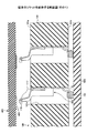
従来より、被接続物を実装基板等と電気的に接続するソケットが知られている。図1は、従来のソケットを例示する断面図(その1)である。図1を参照するに、従来のソケット100は、樹脂を成形したハウジング101と、ばね性を有する導電性の接続端子102とを有する。   Conventionally, a socket for electrically connecting an object to be connected to a mounting board or the like is known. FIG. 1 is a cross-sectional view (part 1) illustrating a conventional socket. Referring to FIG. 1, a conventional socket 100 includes a housing 101 in which a resin is molded and a conductive connection terminal 102 having a spring property.

ハウジング101には、複数の貫通孔101xが所定のピッチで配設されている。接続端子102は、一体的に構成された接続部115及び116とばね部117とを有し、ハウジング101の貫通孔101x内に固定(嵌合)されている。接続部115はハウジング101の一方の面101aから突出しており、接続部116はハウジング101の他方の面101bから露出している。   In the housing 101, a plurality of through holes 101x are arranged at a predetermined pitch. The connection terminal 102 includes integrally formed connection portions 115 and 116 and a spring portion 117, and is fixed (fitted) in the through hole 101 x of the housing 101. The connecting portion 115 protrudes from one surface 101 a of the housing 101, and the connecting portion 116 is exposed from the other surface 101 b of the housing 101.

接続部116は、バンプ103を介して、マザーボード等の実装基板500と電気的に接続されている。電極パッド401を有する被接続物400(例えば、配線基板や半導体パッケージ等)がソケット100の方向に押圧されると、接続部115は電極パッド401と接触する。これにより、ソケット100と被接続物400とは電気的に接続される。すなわち、被接続物400は、ソケット100を介してマザーボード等の実装基板500と電気的に接続される(例えば、特許文献1参照)。   The connection part 116 is electrically connected to a mounting substrate 500 such as a mother board via the bump 103. When an object to be connected 400 having an electrode pad 401 (for example, a wiring board or a semiconductor package) is pressed in the direction of the socket 100, the connecting portion 115 comes into contact with the electrode pad 401. Thereby, the socket 100 and the to-be-connected object 400 are electrically connected. That is, the connected object 400 is electrically connected to the mounting substrate 500 such as a mother board via the socket 100 (see, for example, Patent Document 1).

図2は、従来のソケットを例示する断面図(その2)である。図2を参照するに、従来のソケット200は、基板201と、ばね性を有する導電性の接続端子202及び203とを有する。基板201には複数の貫通孔201xが所定のピッチで配設されている。基板201の一方の面201aには配線204が形成され、配線204は一方の面201aから貫通孔201xを介して他方の面201bに延在している。   FIG. 2 is a cross-sectional view (part 2) illustrating a conventional socket. Referring to FIG. 2, a conventional socket 200 includes a substrate 201 and conductive connection terminals 202 and 203 having spring properties. The substrate 201 has a plurality of through holes 201x arranged at a predetermined pitch. A wiring 204 is formed on one surface 201a of the substrate 201, and the wiring 204 extends from the one surface 201a to the other surface 201b through the through hole 201x.

接続端子202の一端は、基板201の一方の面201aに形成された配線204上に固定されている。接続端子202の他端は、被接続物400の電極パッド401と接触可能に構成されている。接続端子203の一端は、基板201の他方の面201bに形成された配線204上に固定されている。接続端子203の他端は、マザーボード等の実装基板500と電気的に接続されている。なお、接続端子202と接続端子203とは同一部品としても構わない。   One end of the connection terminal 202 is fixed on the wiring 204 formed on one surface 201 a of the substrate 201. The other end of the connection terminal 202 is configured to be in contact with the electrode pad 401 of the connection object 400. One end of the connection terminal 203 is fixed on the wiring 204 formed on the other surface 201 b of the substrate 201. The other end of the connection terminal 203 is electrically connected to a mounting substrate 500 such as a mother board. Note that the connection terminal 202 and the connection terminal 203 may be the same component.

電極パッド401を有する被接続物400(例えば、配線基板や半導体パッケージ等)がソケット200の方向に押圧されると、接続端子202の他端は電極パッド401と接触する。これにより、ソケット200と被接続物400とは電気的に接続される。すなわち、被接続物400は、ソケット200を介してマザーボード等の実装基板500と電気的に接続される(例えば、特許文献2参照)。   When an object to be connected 400 having an electrode pad 401 (for example, a wiring board or a semiconductor package) is pressed in the direction of the socket 200, the other end of the connection terminal 202 is in contact with the electrode pad 401. Thereby, the socket 200 and the to-be-connected object 400 are electrically connected. That is, the connected object 400 is electrically connected to the mounting substrate 500 such as a mother board via the socket 200 (see, for example, Patent Document 2).

米国特許第7264486号明細書US Pat. No. 7,264,486 米国特許第7371073号明細書US Pat. No. 7,371,731

ところで、図1に示すソケット100では、接続端子102の高さがソケット全体の高さを決定している。換言すれば、被接続物400が、ソケット100を介してマザーボード等の実装基板500と電気的に接続される際に、被接続物400と実装基板500との間隔は、接続端子102の高さにより決定される。例えば、被接続物400のソケット100側に背の高い半導体チップやキャパシタ等が実装されており、被接続物400と実装基板500との間隔を図1よりも広げた状態で両者を接続する場合には、接続端子102の形状等を変更して高さを高くする必要があり、設計変更に手間を要する。   By the way, in the socket 100 shown in FIG. 1, the height of the connection terminal 102 determines the height of the whole socket. In other words, when the object to be connected 400 is electrically connected to the mounting substrate 500 such as a mother board via the socket 100, the distance between the object to be connected 400 and the mounting substrate 500 is the height of the connection terminal 102. Determined by. For example, when a tall semiconductor chip, a capacitor, or the like is mounted on the socket 100 side of the connection object 400, and the connection object 400 and the mounting substrate 500 are connected to each other in a state where the interval is wider than that in FIG. In this case, it is necessary to increase the height by changing the shape or the like of the connection terminal 102, and it takes time to change the design.

又、図2に示すソケット200では、接続端子202及び203の高さ及び基板201の厚さがソケット全体の高さを決定している。上記と同様に、例えば、被接続物400のソケット200側に背の高い半導体チップやキャパシタ等が実装されており、被接続物400と実装基板500との間隔を図2よりも広げた状態で両者を接続する場合には、基板201を厚くすれば、接続端子202の形状等を変更する必要はない。しかしながら、基板201を厚くすると、貫通孔201x内の配線204が長くなるため、高速信号伝播に障害が発生する虞がある。   In the socket 200 shown in FIG. 2, the height of the connection terminals 202 and 203 and the thickness of the substrate 201 determine the height of the entire socket. In the same manner as described above, for example, a tall semiconductor chip, a capacitor, or the like is mounted on the socket 200 side of the connection object 400, and the distance between the connection object 400 and the mounting substrate 500 is wider than that in FIG. When both are connected, if the substrate 201 is thickened, it is not necessary to change the shape or the like of the connection terminal 202. However, if the substrate 201 is made thicker, the wiring 204 in the through hole 201x becomes longer, which may cause an obstacle to high-speed signal propagation.

又、ソケット100及び200の何れの場合にも、ソケット全体の高さを細かく調整することは困難であり、被接続物400と実装基板500との間隔を変える必要がある場合に柔軟に対応することができない。   In either case of the sockets 100 and 200, it is difficult to finely adjust the height of the entire socket, and it is possible to flexibly cope with the case where the interval between the connected object 400 and the mounting board 500 needs to be changed. I can't.

本発明は、上記の点に鑑みてなされたものであり、ソケット全体の高さを容易に変更できる接続端子構造、及び前記接続端子構造を有するソケット、並びに前記接続端子構造を有する電子部品パッケージを提供することを課題とする。   The present invention has been made in view of the above points, and includes a connection terminal structure capable of easily changing the height of the entire socket, a socket having the connection terminal structure, and an electronic component package having the connection terminal structure. The issue is to provide.

本接続端子構造の一の形態は、第1面及び前記第1面の反対面である第2面を備えた第1基板と、前記第1基板の第1面に形成された第1電極パッドと、前記第1基板の第2面に形成された第2電極パッドと、第3面及び前記第3面の反対面である第4面を備えた第2基板と、前記第2基板の第3面に形成された第3電極パッドと、前記第2基板の第4面に形成された第4電極パッドと、前記第1基板の第2面と前記第2基板の第3面との間に設けられ、前記第1基板の第2面の外縁部と前記第2基板の第3面の外縁部と接触して前記第1基板と前記第2基板とを接合する支持体と、前記支持体の内側に形成された前記第1基板の第2電極パッドと前記第2基板の第3電極パッドとを電気的に接続するフレキシブル基板と、前記第1電極パッド及び前記第4電極パッドの少なくとも一方と接合された接続端子と、を有することを要件とする。
又、本接続端子構造の他の形態は、第7面及び前記第7面の反対面である第8面を備えた第1補強板と、第9面及び前記第9面の反対面である第10面を備えた第2補強板と、前記第1補強板の第8面と前記第2補強板の第9面との間に設けられ、前記第1補強板と前記第2補強板と接触して前記第1補強板と前記第2補強板とを接合する支持体と、第5面及び前記第5面の反対面である第6面を備え、前記第6面の一端側が前記第1補強板の第7面と接合され、前記第6面の他端側が前記第2補強板の第10面と接合されたフレキシブル基板と、前記フレキシブル基板の第5面の一端側に形成された第1電極パッドと、前記フレキシブル基板の第5面の他端側に形成され、前記第1電極パッドと電気的に接続された第4電極パッドと、前記第1電極パッド及び前記第4電極パッドの少なくとも一方と接合された接続端子と、を有することを要件とする。
One form of this connection terminal structure includes a first substrate having a first surface and a second surface opposite to the first surface, and a first electrode pad formed on the first surface of the first substrate. A second electrode pad formed on the second surface of the first substrate; a third surface; a second surface having a fourth surface opposite to the third surface; and a second substrate of the second substrate. A third electrode pad formed on three surfaces; a fourth electrode pad formed on the fourth surface of the second substrate; and a space between the second surface of the first substrate and the third surface of the second substrate. A support body that contacts the outer edge portion of the second surface of the first substrate and the outer edge portion of the third surface of the second substrate to join the first substrate and the second substrate, and the support A flexible substrate electrically connecting a second electrode pad of the first substrate and a third electrode pad of the second substrate formed inside the body, and the first electrode pad. And the requirement to have a connection terminal that is at least one and joining of the fourth electrode pads.
Moreover, the other form of this connection terminal structure is the 1st reinforcement board provided with the 8th surface which is the 7th surface and the surface opposite to the 7th surface, and the 9th surface and the surface opposite to the 9th surface. A second reinforcing plate having a tenth surface; and provided between an eighth surface of the first reinforcing plate and a ninth surface of the second reinforcing plate, the first reinforcing plate and the second reinforcing plate, A support body that contacts and joins the first reinforcing plate and the second reinforcing plate, and a sixth surface that is the opposite surface of the fifth surface and the fifth surface, and one end side of the sixth surface is the first surface A flexible substrate joined to the seventh surface of one reinforcing plate and the other end of the sixth surface joined to the tenth surface of the second reinforcing plate, and formed on one end of the fifth surface of the flexible substrate A first electrode pad; a fourth electrode pad formed on the other end of the fifth surface of the flexible substrate and electrically connected to the first electrode pad; 1 and the electrode pads and the connection terminals that are at least one and joining of the fourth electrode pads, in that it has a requirement.

本ソケットは、本発明に係る接続端子構造を有し、前記接続端子構造を介して被接続物を着脱可能な状態で他の被接続物に接続することを要件とする。   This socket has a connection terminal structure according to the present invention, and requires that the connection object is connected to another connection object via the connection terminal structure in a detachable state.

本電子部品パッケージは、この順番で積層配置されている被接続物、本発明に係る接続端子構造、及び他の被接続物を有し、前記被接続物と前記他の被接続物とが前記接続端子構造を介して電気的に接続されていることを要件とする。   The electronic component package includes an object to be connected stacked in this order, a connection terminal structure according to the present invention, and another object to be connected, and the object to be connected and the other object to be connected are It is a requirement to be electrically connected through a connection terminal structure.

開示の技術によれば、ソケット全体の高さを容易に変更できる接続端子構造、及び前記接続端子構造を有するソケット、並びに前記接続端子構造を有する電子部品パッケージを提供できる。   According to the disclosed technology, it is possible to provide a connection terminal structure in which the height of the entire socket can be easily changed, a socket having the connection terminal structure, and an electronic component package having the connection terminal structure.

従来のソケットを例示する断面図(その1)である。It is sectional drawing (the 1) which illustrates the conventional socket. 従来のソケットを例示する断面図(その2)である。It is sectional drawing (the 2) which illustrates the conventional socket. 第1の実施の形態に係る接続端子構造を例示する斜視図である。It is a perspective view which illustrates the connection terminal structure concerning a 1st embodiment. 第1の実施の形態に係る接続端子構造を例示する分解斜視図である。1 is an exploded perspective view illustrating a connection terminal structure according to a first embodiment. 第1の実施の形態に係る接続端子構造を例示する断面図である。It is sectional drawing which illustrates the connection terminal structure which concerns on 1st Embodiment. 第1の実施の形態に係る接続端子構造を例示する平面図である。It is a top view which illustrates the connection terminal structure concerning a 1st embodiment. 第1の実施の形態に係る接続端子を例示する断面図である。It is sectional drawing which illustrates the connecting terminal which concerns on 1st Embodiment. 第1の実施の形態に係る接続端子構造の製造方法を例示する図(その1)である。FIG. 6 is a diagram (part 1) illustrating the method for manufacturing the connection terminal structure according to the first embodiment; 第1の実施の形態に係る接続端子構造の製造方法を例示する図(その2)である。FIG. 6 is a second diagram illustrating the method for manufacturing the connection terminal structure according to the first embodiment; 第1の実施の形態に係る接続端子構造の製造方法を例示する図(その3)である。FIG. 6 is a diagram (part 3) illustrating the method for manufacturing the connection terminal structure according to the first embodiment; 第1の実施の形態の変形例1に係る接続端子構造を例示する断面図である。It is sectional drawing which illustrates the connection terminal structure which concerns on the modification 1 of 1st Embodiment. 第1の実施の形態の変形例2に係る接続端子構造を例示する断面図である。It is sectional drawing which illustrates the connection terminal structure which concerns on the modification 2 of 1st Embodiment. 第1の実施の形態の変形例3に係る接続端子構造を例示する断面図である。It is sectional drawing which illustrates the connection terminal structure which concerns on the modification 3 of 1st Embodiment. 第1の実施の形態の変形例3に係る接続端子構造を例示する平面図である。It is a top view which illustrates the connection terminal structure concerning the modification 3 of a 1st embodiment. 検査の対象となる半導体パッケージを例示する断面図(その1)である。It is sectional drawing (the 1) which illustrates the semiconductor package used as the test object. 半導体パッケージを電気的に検査する際の接続例を示す断面図(その1)である。It is sectional drawing (the 1) which shows the example of a connection at the time of electrically test | inspecting a semiconductor package. 検査の対象となる半導体パッケージを例示する断面図(その2)である。It is sectional drawing (the 2) which illustrates the semiconductor package used as the test object. 半導体パッケージを電気的に検査する際の接続例を示す断面図(その2)である。It is sectional drawing (the 2) which shows the example of a connection at the time of electrically test | inspecting a semiconductor package. 検査の対象となる半導体パッケージを例示する断面図(その3)である。FIG. 10 is a cross-sectional view (part 3) illustrating a semiconductor package to be inspected; 半導体パッケージを電気的に検査する際の接続例を示す断面図(その3)である。FIG. 10 is a cross-sectional view (part 3) illustrating a connection example when the semiconductor package is electrically inspected. 第3の実施の形態に係る半導体パッケージを例示する断面図である。10 is a cross-sectional view illustrating a semiconductor package according to a third embodiment; FIG.

以下、図面を参照して発明を実施するための形態について説明する。なお、各図面において、同一構成部分には同一符号を付し、重複した説明を省略する場合がある。   Hereinafter, embodiments for carrying out the invention will be described with reference to the drawings. In addition, in each drawing, the same code | symbol is attached | subjected to the same component and the overlapping description may be abbreviate | omitted.

なお、以下の実施の形態及びその変形例では、一例として、半導体パッケージ及び基板の平面形状が矩形状である場合を示すが、半導体パッケージ及び基板の平面形状は矩形状には限定されず、任意の形状として構わない。   Note that, in the following embodiments and modifications thereof, as an example, the planar shape of the semiconductor package and the substrate is a rectangular shape, but the planar shape of the semiconductor package and the substrate is not limited to a rectangular shape, and is arbitrary. It does not matter as the shape.
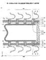
〈第1の実施の形態〉
[第1の実施の形態に係る接続端子構造]
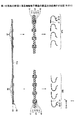
図3は、第1の実施の形態に係る接続端子構造を例示する斜視図である。図4は、第1の実施の形態に係る接続端子構造を例示する分解斜視図である。図5は、第1の実施の形態に係る接続端子構造を例示する断面図である。図6は、第1の実施の形態に係る接続端子構造を例示する平面図である。なお、図5は、図6の各接続端子30の配設方向Cに平行な断面を示している。但し、図6に示すように、平面視において各接続端子30は配設方向Cに対して傾いているため、配設方向Cに平行な断面図では接続端子30の断面形状を示すことができない。そこで、便宜上、図5では、配設方向Cに対してθ傾斜した方向に平行な接続端子30の断面形状を模式的に示している(以降の断面図でも同様)。
<First Embodiment>
[Connection Terminal Structure According to First Embodiment]
FIG. 3 is a perspective view illustrating the connection terminal structure according to the first embodiment. FIG. 4 is an exploded perspective view illustrating the connection terminal structure according to the first embodiment. FIG. 5 is a cross-sectional view illustrating the connection terminal structure according to the first embodiment. FIG. 6 is a plan view illustrating the connection terminal structure according to the first embodiment. FIG. 5 shows a cross section parallel to the arrangement direction C of each connection terminal 30 in FIG. However, as shown in FIG. 6, since each connection terminal 30 is inclined with respect to the arrangement direction C in a plan view, the cross-sectional view parallel to the arrangement direction C cannot show the cross-sectional shape of the connection terminal 30. . Therefore, for convenience, in FIG. 5, (also in cross section after) the cross-sectional shape of the array direction C relative theta 1 inclined direction connecting terminals 30 parallel to the in and shown schematically.

図3〜図6を参照するに、接続端子構造10は、大略すると、2枚の基板20と、接続端子群30Aと、接続端子群30Bと、接合部40及び41と、フレキシブル基板50と、支持体55とを有する。   Referring to FIGS. 3 to 6, the connection terminal structure 10 generally includes two substrates 20, a connection terminal group 30 </ b> A, a connection terminal group 30 </ b> B, joint portions 40 and 41, a flexible substrate 50, And a support 55.

接続端子構造10において、接続端子群30Aは、一方の基板20を介して、フレキシブル基板50の一端側に接合されている。又、接続端子群30Bは、他方の基板20を介して、フレキシブル基板50の他端側に接合されている。一方の基板20と他方の基板20とは略平行となるように支持体55に固定されており、接続端子群30Aの各接続端子30の接続部32と接続端子群30Bの各接続端子30の接続部32とは互いに反対方向を向いている。なお、接続端子群30A及び接続端子群30Bは、それぞれ同一数の接続端子30が同一規則で配列されたものであるが、便宜上別符号としている。以下、接続端子構造10の構成要素について詳説する。   In the connection terminal structure 10, the connection terminal group 30 </ b> A is bonded to one end side of the flexible substrate 50 via one substrate 20. The connection terminal group 30 </ b> B is bonded to the other end side of the flexible substrate 50 via the other substrate 20. One substrate 20 and the other substrate 20 are fixed to the support body 55 so as to be substantially parallel to each other, and the connection portions 32 of the connection terminals 30 of the connection terminal group 30A and the connection terminals 30 of the connection terminal group 30B. The connection portions 32 face in opposite directions. Note that the connection terminal group 30A and the connection terminal group 30B have the same number of connection terminals 30 arranged in accordance with the same rule. Hereinafter, the components of the connection terminal structure 10 will be described in detail.

各基板20は、基板本体21と、基板本体21の一方の面21aに形成された複数の電極パッド22と、他方の面21bに形成された複数の電極パッド23と、基板本体21の一方の面21aから他方の面21bに貫通する貫通孔21x内に形成された貫通配線24とを有する。各電極パッド22は、接続端子30の位置に対応して例えばペリフェラル状やエリアアレイ状に配列されている。各電極パッド23は、基板本体21を介して、各電極パッド22と対向する位置に配列されている。基板本体21を介して対向する位置に形成された電極パッド22と電極パッド23とは、貫通配線24を介して電気的に接続されている。   Each substrate 20 includes a substrate body 21, a plurality of electrode pads 22 formed on one surface 21a of the substrate body 21, a plurality of electrode pads 23 formed on the other surface 21b, and one of the substrate bodies 21. And a through-wiring 24 formed in the through-hole 21x penetrating from the surface 21a to the other surface 21b. Each electrode pad 22 is arranged in a peripheral shape or an area array shape, for example, corresponding to the position of the connection terminal 30. Each electrode pad 23 is arranged at a position facing each electrode pad 22 through the substrate body 21. The electrode pad 22 and the electrode pad 23 formed at positions facing each other through the substrate body 21 are electrically connected through the through wiring 24.

基板本体21は、接続端子30を固定するための基体となるものであり、例えば、ガラスクロスにエポキシ系樹脂等の絶縁性樹脂を含浸したリジッドな基板(例えば、FR4材等)を用いることができる。基板本体21の平面形状は、例えば、矩形状とすることができる。基板本体21の厚さは、例えば、0.2〜0.8mm程度とすることができる。   The substrate body 21 serves as a base for fixing the connection terminals 30. For example, a rigid substrate (for example, FR4 material) in which an insulating resin such as an epoxy resin is impregnated into a glass cloth is used. it can. The planar shape of the substrate body 21 can be, for example, a rectangular shape. The thickness of the substrate body 21 can be set to, for example, about 0.2 to 0.8 mm.

電極パッド22、電極パッド23、及び貫通配線24の材料としては、例えば、銅(Cu)等を用いることができる。電極パッド22、電極パッド23の厚さは、例えば、5〜10μm程度とすることができる。電極パッド22、電極パッド23、及び貫通配線24は、例えば、セミアディティブ法やサブトラクティブ法等の各種配線形成方法により形成できる。なお、電極パッド22の一部を露出するソルダーレジスト層を設けても構わない。同様に、電極パッド23の一部を露出するソルダーレジスト層を設けても構わない。   As a material of the electrode pad 22, the electrode pad 23, and the through wiring 24, for example, copper (Cu) or the like can be used. The thickness of the electrode pad 22 and the electrode pad 23 can be set to about 5 to 10 μm, for example. The electrode pad 22, the electrode pad 23, and the through wiring 24 can be formed by various wiring forming methods such as a semi-additive method and a subtractive method. A solder resist layer that exposes part of the electrode pad 22 may be provided. Similarly, a solder resist layer that exposes a part of the electrode pad 23 may be provided.

接続端子群30A及び接続端子群30Bは、それぞれ複数の接続端子30が所定の規則で配列されたものである。接続端子群30A及び接続端子群30Bに含まれる各接続端子30は、ばね性を有する導電性の部材である。接続端子30の一端である固定部31は、接合部40を介して電極パッド22と電気的及び機械的に接続されている。接続端子30の他端である接続部32は、被接続物の電極パッド等に離間可能な状態(固定されていない状態)で当接し、被接続物の電極パッド等と電気的に接続される部分である。   Each of the connection terminal group 30A and the connection terminal group 30B has a plurality of connection terminals 30 arranged in a predetermined rule. Each connection terminal 30 included in the connection terminal group 30A and the connection terminal group 30B is a conductive member having a spring property. The fixing portion 31 that is one end of the connection terminal 30 is electrically and mechanically connected to the electrode pad 22 via the joint portion 40. The connection portion 32, which is the other end of the connection terminal 30, comes into contact with an electrode pad or the like of the connected object in a separable state (non-fixed state) and is electrically connected to the electrode pad or the like of the connected object. Part.

接続端子群30A及び接続端子群30Bにおいて、各接続端子30は、平面視において、各接続端子30の配設方向Cに対して所定の角度θをなして傾くように配列されている(図6参照)。所定の角度θは、例えば、25〜35度程度とすることができる。このように、各接続端子30を、各接続端子30の配設方向Cに対して傾斜させて配列することにより、配設方向Cに対して平行に配列した場合と比較して、単位面積当たりに多くの接続端子30を配列することが可能となる。これにより、例えば0.4mm程度の狭ピッチで電極パッド(例えば、後述の電極パッド64等)が配列された被接続物(例えば、後述の半導体パッケージ60A等)にも対応可能となる。なお、接続端子30の詳細な構造については、後述する。 In the connection terminal group 30A and the connection terminal group 30B, the connection terminals 30 are arranged so as to be inclined at a predetermined angle θ 1 with respect to the arrangement direction C of the connection terminals 30 in plan view (FIG. 6). The predetermined angle θ 1 can be set to about 25 to 35 degrees, for example. In this way, by arranging the connection terminals 30 so as to be inclined with respect to the arrangement direction C of the connection terminals 30, compared to the case where the connection terminals 30 are arranged in parallel to the arrangement direction C, the unit per unit area. It is possible to arrange a large number of connection terminals 30. Accordingly, it is possible to deal with an object to be connected (for example, a semiconductor package 60A described later) in which electrode pads (for example, an electrode pad 64 described later) are arranged at a narrow pitch of about 0.4 mm, for example. The detailed structure of the connection terminal 30 will be described later.

接合部40は、電極パッド22上に形成され、接続端子群30Aの接続端子30の固定部31と電極パッド22とを電気的及び機械的に接続している。接合部40の材料としては、はんだや導電性樹脂ペースト(例えば、Agペースト)等の導電性材料を用いることができる。接合部40の材料としてはんだを用いる場合は、例えば、Pbを含む合金、SnとCuの合金、SnとAgの合金、SnとAgとCuの合金等を用いることができる。   The joint portion 40 is formed on the electrode pad 22 and electrically and mechanically connects the fixing portion 31 of the connection terminal 30 of the connection terminal group 30A and the electrode pad 22. As a material of the joint portion 40, a conductive material such as solder or a conductive resin paste (for example, Ag paste) can be used. When solder is used as the material of the joint portion 40, for example, an alloy containing Pb, an alloy of Sn and Cu, an alloy of Sn and Ag, an alloy of Sn, Ag, and Cu can be used.

フレキシブル基板50は、基板本体51と、複数の電極パッド52及び53とを有するフレキシブルなフィルム状基板である。各電極パッド52は、基板本体51の一方の面51aの一端側に形成されており、接合部41を介して、フレキシブル基板50の一方の面51aの一端側に積層された一方の基板20の各電極パッド23と電気的に接続されている。各電極パッド53は、基板本体51の一方の面51aの他端側に形成されており、接合部41を介して、フレキシブル基板50の一方の面51aの他端側に積層された他方の基板20の各電極パッド23と電気的に接続されている。接合部41の材料としては、はんだや導電性樹脂ペースト(例えば、Agペースト)等の導電性材料を用いることができる。接合部41の材料としてはんだを用いる場合は、例えば、Pbを含む合金、SnとCuの合金、SnとAgの合金、SnとAgとCuの合金等を用いることができる。   The flexible substrate 50 is a flexible film substrate having a substrate body 51 and a plurality of electrode pads 52 and 53. Each electrode pad 52 is formed on one end side of one surface 51 a of the substrate body 51, and is connected to one end side of one surface 51 a of the flexible substrate 50 via the bonding portion 41. Each electrode pad 23 is electrically connected. Each electrode pad 53 is formed on the other end side of one surface 51 a of the substrate body 51, and the other substrate stacked on the other end side of the one surface 51 a of the flexible substrate 50 via the bonding portion 41. The 20 electrode pads 23 are electrically connected. As a material of the joint portion 41, a conductive material such as solder or conductive resin paste (for example, Ag paste) can be used. When solder is used as the material of the joint portion 41, for example, an alloy containing Pb, an alloy of Sn and Cu, an alloy of Sn and Ag, an alloy of Sn, Ag, and Cu can be used.

フレキシブル基板50は、電極パッド52が形成されている領域(一方の面51aの一端側)と、電極パッド53が形成されている領域(一方の面51aの他端側)との間で折り曲げられ、各電極パッド52と各電極パッド53とは、平面視において略重複する位置に配置されている。平面視において略重複する位置に配置されている電極パッド52と電極パッド53とは、基板本体51の一方の面51aや基板本体51の内層等に形成された配線パターン(図示せず)により電気的に接続されている。   The flexible substrate 50 is bent between a region where the electrode pad 52 is formed (one end side of the one surface 51a) and a region where the electrode pad 53 is formed (the other end side of the one surface 51a). The electrode pads 52 and the electrode pads 53 are disposed at substantially overlapping positions in plan view. The electrode pad 52 and the electrode pad 53 arranged at substantially overlapping positions in plan view are electrically connected by a wiring pattern (not shown) formed on one surface 51a of the substrate body 51, an inner layer of the substrate body 51, or the like. Connected.

基板本体51としては、例えば、各基板20よりも柔軟性が高いポリイミド樹脂や液晶ポリマ等の材料を用いることができる。基板本体51の平面形状(折り曲げていない状態)は、例えば、短冊状とすることができる。基板本体51の厚さは、例えば、50〜200μm程度とすることができる。   As the substrate body 51, for example, a material such as a polyimide resin or a liquid crystal polymer having higher flexibility than each substrate 20 can be used. The planar shape (unbent state) of the substrate body 51 can be, for example, a strip shape. The thickness of the substrate body 51 can be set to, for example, about 50 to 200 μm.

電極パッド52及び53の材料としては、例えば、銅(Cu)等を用いることができる。電極パッド52及び53の厚さは、例えば、5〜10μm程度とすることができる。電極パッド52及び53は、例えば、セミアディティブ法やサブトラクティブ法等の各種配線形成方法により形成できる。なお、電極パッド52及び53の一部を露出するソルダーレジスト層を設けても構わない。   As a material of the electrode pads 52 and 53, for example, copper (Cu) or the like can be used. The thickness of the electrode pads 52 and 53 can be set to about 5 to 10 μm, for example. The electrode pads 52 and 53 can be formed by various wiring forming methods such as a semi-additive method and a subtractive method. A solder resist layer that exposes part of the electrode pads 52 and 53 may be provided.

このように、接続端子群30Aの各接続端子30は、一方の基板20、フレキシブル基板50、及び他方の基板20を介して、接続端子群30Bの対応する各接続端子30と電気的に接続されている。なお、接続端子群30Bの対応する各接続端子30とは、接続端子群30Aの各接続端子30と平面視において略重複する位置に配置された接続端子30を指す。   Thus, each connection terminal 30 of the connection terminal group 30A is electrically connected to each corresponding connection terminal 30 of the connection terminal group 30B via the one substrate 20, the flexible substrate 50, and the other substrate 20. ing. Note that the corresponding connection terminals 30 of the connection terminal group 30B refer to the connection terminals 30 arranged at positions substantially overlapping with the connection terminals 30 of the connection terminal group 30A in plan view.

支持体55は、平面形状が略コの字型で高さが略一定の部材である。支持体55は、一方の基板20と他方の基板20との間に配置されている。支持体55は、一方の基板20及び他方の基板20を外側に向けて、一方の面51aの一端側と他端側とが対向するようにフレキシブル基板50を折り曲げた状態で、一方の基板20及び他方の基板20を支持している。又、支持体55は、接続端子群30Aの各接続端子30と接続端子群30Bの各接続端子30との間隔(高さ)を規定している。支持体55の上端面55aは、例えば、接着剤(図示せず)を介して、一方の基板20の下面外縁部と接合されている。支持体55の下端面55bは、例えば、接着剤(図示せず)を介して、他方の基板20の上面外縁部と接合されている。支持体55は、例えば、アルミニウム(Al)やステンレス(SUS)等の金属材料や、エポキシ樹脂等を主成分とする樹脂材料等により形成できる。なお、支持体55と一方の基板20及び他方の基板20とは、接着剤を用いずに、圧入やねじ止め等により固定しても構わない。支持体55の高さ(一方の基板20と他方の基板20との間隔)は、例えば、5mm以上とすることができる。   The support body 55 is a member having a substantially U-shaped planar shape and a substantially constant height. The support body 55 is disposed between the one substrate 20 and the other substrate 20. The support body 55 has the one substrate 20 and the other substrate 20 facing outward, and the flexible substrate 50 is folded so that one end side and the other end side of the one surface 51a face each other. And the other substrate 20 is supported. The support body 55 defines the distance (height) between each connection terminal 30 of the connection terminal group 30A and each connection terminal 30 of the connection terminal group 30B. The upper end surface 55a of the support body 55 is joined to the outer edge of the lower surface of the one substrate 20 through, for example, an adhesive (not shown). The lower end surface 55b of the support body 55 is joined to the outer edge portion of the upper surface of the other substrate 20 through, for example, an adhesive (not shown). The support 55 can be formed of, for example, a metal material such as aluminum (Al) or stainless steel (SUS), a resin material mainly composed of an epoxy resin, or the like. The support 55, the one substrate 20, and the other substrate 20 may be fixed by press-fitting, screwing, or the like without using an adhesive. The height of the support 55 (the distance between the one substrate 20 and the other substrate 20) can be set to 5 mm or more, for example.

ここで、図7を参照しながら、接続端子30の詳細な構造について説明する。図7は、第1の実施の形態に係る接続端子を例示する断面図である。図7を参照するに、接続端子30は、ばね性を有する導電性の部材であり、固定部31と、接続部32と、ばね部33と、第1支持部34と、第2支持部35とを有する。   Here, the detailed structure of the connection terminal 30 will be described with reference to FIG. FIG. 7 is a cross-sectional view illustrating the connection terminals according to the first embodiment. Referring to FIG. 7, the connection terminal 30 is a conductive member having a spring property, and includes a fixing portion 31, a connection portion 32, a spring portion 33, a first support portion 34, and a second support portion 35. And have.

固定部31は、接続端子30の一端に形成されている。固定部31は、板状とされている。固定部31の厚さ(Z方向)は、例えば0.08mm程度とすることができる。固定部31の横幅(Y方向)は、例えば0.4mm程度とすることができる。固定部31の縦幅(X方向)は、例えば0.4mm程度とすることができる。   The fixing portion 31 is formed at one end of the connection terminal 30. The fixing portion 31 is plate-shaped. The thickness (Z direction) of the fixing portion 31 can be set to, for example, about 0.08 mm. The lateral width (Y direction) of the fixing portion 31 can be set to, for example, about 0.4 mm. The vertical width (X direction) of the fixing portion 31 can be set to, for example, about 0.4 mm.

接続部32は、接続端子30の他端に形成され、固定部31と対向するように配置されている。接続部32は、ばね部33、第1支持部34、及び第2支持部35を介して、固定部31と電気的に接続されている。接続部32は、当接部38と、突出部39とを有する。接続部32の厚さは、例えば0.08mm程度とすることができる。接続部32の横幅(Y方向)は、例えば、0.2mm程度とすることができる。なお、ばね部33、第1支持部34、及び第2支持部35を、接続端子30の湾曲部と称する場合がある。   The connection portion 32 is formed at the other end of the connection terminal 30 and is disposed so as to face the fixed portion 31. The connection part 32 is electrically connected to the fixed part 31 via the spring part 33, the first support part 34, and the second support part 35. The connection part 32 has a contact part 38 and a protrusion part 39. The thickness of the connection part 32 can be about 0.08 mm, for example. The horizontal width (Y direction) of the connection part 32 can be about 0.2 mm, for example. In addition, the spring part 33, the 1st support part 34, and the 2nd support part 35 may be called the curved part of the connection terminal 30. FIG.

当接部38は、被接続物の電極パッド(例えば、後述する半導体パッケージ60Aの電極パッド64等)と当接する部分である。当接部38はラウンド形状とされており、接続端子30が押圧された際、主にZ方向に移動する。このように、当接部38をラウンド形状とすることにより、当接部38が押圧され電極パッド64等と当接する際、当接部38により電極パッド64等が破損することを防止できる。   The abutting portion 38 is a portion that abuts on an electrode pad of an object to be connected (for example, an electrode pad 64 of a semiconductor package 60A described later). The contact portion 38 has a round shape and moves mainly in the Z direction when the connection terminal 30 is pressed. Thus, by making the contact portion 38 round, it is possible to prevent the electrode pad 64 and the like from being damaged by the contact portion 38 when the contact portion 38 is pressed and contacted with the electrode pad 64 and the like.

又、当接部38は、例えば半導体パッケージ60Aが接続部32を押圧した際、ばね部33の変形により、接続部32が固定部31に近づく方向(Z方向)に移動した状態で、電極パッド64等と当接する。これにより、電極パッド64等と接続部32とが当接した際、接続部32が、電極パッド64等が形成された面と平行な方向に大きく移動することがなくなるため、電極パッド64等を狭ピッチに配置できる。電極パッド64等のピッチ(当接部38のピッチ)は、例えば、0.4〜1.5mm程度とすることができる。   Also, the contact portion 38 is an electrode pad in a state in which, for example, when the semiconductor package 60 </ b> A presses the connection portion 32, the connection portion 32 moves in the direction approaching the fixed portion 31 (Z direction) due to deformation of the spring portion 33. 64 etc. As a result, when the electrode pad 64 or the like and the connection portion 32 abut, the connection portion 32 does not move greatly in a direction parallel to the surface on which the electrode pad 64 or the like is formed. Can be arranged at a narrow pitch. The pitch of the electrode pads 64 and the like (the pitch of the contact portions 38) can be set to about 0.4 to 1.5 mm, for example.

突出部39は、一方の端部が第2支持部35と一体的に形成されており、他方の端部が当接部38と一体的に形成されている。突出部39は、第2支持部35から電極パッド64等に向かう方向(固定部31から離間する方向)に突出している。   One end of the projecting portion 39 is formed integrally with the second support portion 35, and the other end is formed integrally with the contact portion 38. The protruding portion 39 protrudes in the direction from the second support portion 35 toward the electrode pad 64 (a direction away from the fixed portion 31).

このように、当接部38と第2支持部35との間に、当接部38及び第2支持部35と一体的に形成され、第2支持部35から電極パッド64等に向かう方向(固定部31から離間する方向)に突出する突出部39を設けることにより、以下の効果を奏する。すなわち、半導体パッケージ60A等が当接部38を押圧した際の、ばね部33の変形による電極パッド64等と第2支持部35との接触を防止することが可能となり、接続端子30及び電極パッド64等の破損を防止できる。   In this way, the contact portion 38 and the second support portion 35 are formed integrally with the contact portion 38 and the second support portion 35, and the direction from the second support portion 35 toward the electrode pad 64 and the like ( By providing the projecting portion 39 projecting in a direction away from the fixing portion 31, the following effects can be obtained. That is, when the semiconductor package 60A or the like presses the contact portion 38, it is possible to prevent the electrode pad 64 or the like from contacting the second support portion 35 due to the deformation of the spring portion 33, and the connection terminal 30 and the electrode pad. Damage to 64 etc. can be prevented.

電極パッド64等と接続部32とが当接していない状態における接続部32の突出量D(第2支持部35と突出部39との接続部分を基準としたときの突出量)は、例えば、0.3mmとすることができる。   The protruding amount D of the connecting portion 32 in the state where the electrode pad 64 and the like and the connecting portion 32 are not in contact (the protruding amount with respect to the connecting portion between the second support portion 35 and the protruding portion 39) is, for example, It can be 0.3 mm.

ばね部33は、第1支持部34と第2支持部35との間に配置されており、第1支持部34及び第2支持部35と一体的に形成されている。ばね部33は、湾曲した形状(例えば、C字型)とされており、ばね性を有する。   The spring portion 33 is disposed between the first support portion 34 and the second support portion 35 and is formed integrally with the first support portion 34 and the second support portion 35. The spring portion 33 has a curved shape (for example, a C shape) and has a spring property.

ばね部33は、半導体パッケージ60A等により接続部32が押圧された際、接続部32を電極パッド64等に向かう方向に反発させることで、接続部32と電極パッド64等とを固定することなく接触させるためのものである。ばね部33の横幅(Y方向)及び厚さは、例えば、接続部32の横幅(Y方向)及び厚さと同じにすることができる。   The spring part 33 repels the connection part 32 in the direction toward the electrode pad 64 etc. when the connection part 32 is pressed by the semiconductor package 60 </ b> A etc., so that the connection part 32 and the electrode pad 64 etc. are not fixed. It is for making it contact. The lateral width (Y direction) and thickness of the spring part 33 can be made the same as the lateral width (Y direction) and thickness of the connection part 32, for example.

なお、本実施の形態の接続端子30では、実際には、第1支持部34、ばね部33、第2支持部35、及び接続部32が一体的にばねとして機能する。第1支持部34、ばね部33、第2支持部35、及び接続部32に対応する部分の接続端子30のばね定数は、例えば、0.6〜0.8N/mmとすることができる。   In the connection terminal 30 of the present embodiment, the first support part 34, the spring part 33, the second support part 35, and the connection part 32 actually function as a spring integrally. The spring constant of the connection terminal 30 corresponding to the first support part 34, the spring part 33, the second support part 35, and the connection part 32 can be set to 0.6 to 0.8 N / mm, for example.

第1支持部34は、ばね部33と固定部31との間に配置されている。第1支持部34の一方の端部は、ばね部33の一方の端部と一体的に形成されており、第1支持部34の他方の端部は、固定部31と一体的に形成されている。第1支持部34は、板状とされている。   The first support portion 34 is disposed between the spring portion 33 and the fixed portion 31. One end portion of the first support portion 34 is formed integrally with one end portion of the spring portion 33, and the other end portion of the first support portion 34 is formed integrally with the fixing portion 31. ing. The first support portion 34 has a plate shape.

第1支持部34は、固定部31の面31aを含む平面Eと、基板20と対向する側の第1支持部34の面34aとが成す角度θが鋭角となるように形成されている。角度θは、例えば、5〜15度とすることができる。 The first support portion 34 is formed such that an angle θ 2 formed by the plane E including the surface 31 a of the fixing portion 31 and the surface 34 a of the first support portion 34 on the side facing the substrate 20 is an acute angle. . Angle theta 2 may be, for example, 5 to 15 degrees.

このように、角度θを鋭角にすることで、半導体パッケージ60A等が当接部38を押圧した際のばね部33の変形による基板20と第1支持部34との接触を防止することが可能となるため、接続端子30及び基板20の破損を防止できる。第1支持部34の横幅(Y方向)及び厚さは、例えば、接続部32の横幅(Y方向)及び厚さと同じにすることができる。 In this way, by the angle theta 2 at an acute angle, it is possible to prevent the contact between the substrate 20 and the first support portion 34 semiconductor package 60A or the like by the deformation of the spring portion 33 at the time when pressed contact portion 38 Therefore, the connection terminal 30 and the substrate 20 can be prevented from being damaged. For example, the lateral width (Y direction) and thickness of the first support portion 34 can be made the same as the lateral width (Y direction) and thickness of the connection portion 32.

第2支持部35は、ばね部33と接続部32との間に配置されている。第2支持部35の一方の端部は、ばね部33の他方の端部と一体的に形成されており、第2支持部35の他方の端部は、接続部32の突出部39と一体的に形成されている。第2支持部35は、板状とされている。第2支持部35の横幅(Y方向)及び厚さは、例えば、接続部32の横幅(Y方向)及び厚さと同じにすることができる。   The second support part 35 is disposed between the spring part 33 and the connection part 32. One end portion of the second support portion 35 is formed integrally with the other end portion of the spring portion 33, and the other end portion of the second support portion 35 is integrated with the protruding portion 39 of the connection portion 32. Is formed. The 2nd support part 35 is made into plate shape. The lateral width (Y direction) and thickness of the second support part 35 can be made the same as the lateral width (Y direction) and thickness of the connection part 32, for example.

図7に示す状態(接続端子30の接続部32が押圧されていない状態)における接続端子30の高さHは、例えば、1〜2mm程度とすることができる。   The height H of the connection terminal 30 in the state shown in FIG. 7 (a state where the connection portion 32 of the connection terminal 30 is not pressed) can be set to, for example, about 1 to 2 mm.

[第1の実施の形態に係る接続端子構造の製造方法]
次に、図8〜図10を参照しながら、接続端子構造10の製造方法について説明する。図8〜図10は、第1の実施の形態に係る接続端子構造の製造方法を例示する図である。なお、図8において、基板20等は図5等とは上下が反転した状態で描かれている。
[Method for Manufacturing Connection Terminal Structure According to First Embodiment]
Next, a manufacturing method of the connection terminal structure 10 will be described with reference to FIGS. 8 to 10 are views illustrating the method for manufacturing the connection terminal structure according to the first embodiment. In FIG. 8, the substrate 20 and the like are depicted in a state where the top and bottom are reversed from those of FIG.

まず、図8に示す工程では、接続端子群30Aとなる各接続端子30(本実施の形態では16個)及び接続端子群30Bとなる各接続端子30(本実施の形態では16個)と、電極パッド22上に接合部40が形成され電極パッド23上に接合部41が形成された2枚の基板20と、1枚のフレキシブル基板50とを準備し、それらを所定の状態に配置する。   First, in the process shown in FIG. 8, each connection terminal 30 (16 in the present embodiment) to be the connection terminal group 30A and each connection terminal 30 (16 in the present embodiment) to be the connection terminal group 30B; Two substrates 20 each having a bonding portion 40 formed on the electrode pad 22 and a bonding portion 41 formed on the electrode pad 23 and one flexible substrate 50 are prepared and arranged in a predetermined state.

具体的には、接続端子群30Aとなる各接続端子30を、固定部31を上側に向けて、所定の配列用治具(図示せず)に仮固定する。又、接続端子群30Bとなる各接続端子30を、固定部31を上側に向けて、所定の配列用治具(図示せず)に仮固定する。そして、接続端子群30Aの各接続端子30の固定部31上に接合部40を介して一方の基板20の電極パッド22を接触させ、接続端子群30Bの各接続端子30の固定部31上に接合部40を介して他方の基板20の電極パッド22を接触させる。更に、接合部41を介して一方の基板20の電極パッド23をフレキシブル基板50の電極パッド52と接触させ、接合部41を介して他方の基板20の電極パッド23をフレキシブル基板50の電極パッド53と接触させる。   Specifically, each connection terminal 30 to be the connection terminal group 30A is temporarily fixed to a predetermined arrangement jig (not shown) with the fixing portion 31 facing upward. Further, each connection terminal 30 to be the connection terminal group 30B is temporarily fixed to a predetermined arrangement jig (not shown) with the fixing portion 31 facing upward. And the electrode pad 22 of one board | substrate 20 is made to contact via the junction part 40 on the fixing | fixed part 31 of each connecting terminal 30 of the connecting terminal group 30A, and on the fixing | fixed part 31 of each connecting terminal 30 of the connecting terminal group 30B. The electrode pad 22 of the other substrate 20 is brought into contact with the bonding portion 40. Further, the electrode pad 23 of one substrate 20 is brought into contact with the electrode pad 52 of the flexible substrate 50 through the joint portion 41, and the electrode pad 23 of the other substrate 20 is brought into contact with the electrode pad 53 of the flexible substrate 50 through the joint portion 41. Contact with.

なお、基板20及びフレキシブル基板50は周知の方法により作製でき、接続端子30は、例えば、以下のようにして作製できる。すなわち、図示していない金属板(例えば、リン青銅やベリリウム銅、コルソン系の銅合金等のCu系合金)を準備し、準備した金属板を所定の形状に打ち抜き加工する。この際、例えば、長尺状に打ち抜く。その後、打ち抜き加工された金属板の表面全体にNiめっき膜(例えば、厚さ1〜3μm)を形成し、更に、固定部31及び接続部32に対応する部分に形成されたNiめっき膜に、Auめっき膜(例えば、厚さ0.3〜0.5μm)を積層形成(Auめっき膜を部分的に形成)する。その後、Niめっき膜及びAuめっき膜が形成された金属板を曲げ加工することで接続端子30が完成する。なお、接続端子30は、図示していない金属板を所定の形状にエッチング加工した後、エッチング加工された金属板を曲げ加工することで形成してもよい。   In addition, the board | substrate 20 and the flexible substrate 50 can be produced by a well-known method, and the connection terminal 30 can be produced as follows, for example. That is, a metal plate (not shown) (for example, a Cu-based alloy such as phosphor bronze, beryllium copper, or a Corson-based copper alloy) is prepared, and the prepared metal plate is punched into a predetermined shape. At this time, for example, it is punched into a long shape. Thereafter, a Ni plating film (for example, a thickness of 1 to 3 μm) is formed on the entire surface of the punched metal plate, and further, a Ni plating film formed on a portion corresponding to the fixing portion 31 and the connection portion 32 is used. An Au plating film (for example, a thickness of 0.3 to 0.5 μm) is formed by lamination (partially forming the Au plating film). Thereafter, the connection terminal 30 is completed by bending the metal plate on which the Ni plating film and the Au plating film are formed. The connection terminal 30 may be formed by etching a metal plate (not shown) into a predetermined shape and then bending the etched metal plate.

次に、図9に示す工程では、図8に示す構造体を相互に接合する。具体的には、所定の配列用治具(図示せず)も含めた図8に示す構造体をリフロー炉に通して例えば230℃程度に加熱し、はんだや導電性樹脂ペースト(例えば、Agペースト)等の導電性材料である接合部40及び接合部41を溶融させた後、常温に戻して硬化させる。その後、所定の配列用治具(図示せず)を取り外すことにより、図8に示す構造体が相互に接合された図9に示す構造体が作製される。なお、図8と図9とは上下が反転した状態で描かれている。   Next, in the step shown in FIG. 9, the structures shown in FIG. 8 are bonded to each other. Specifically, the structure shown in FIG. 8 including a predetermined arrangement jig (not shown) is passed through a reflow furnace and heated to, for example, about 230 ° C., and solder or conductive resin paste (for example, Ag paste) ) And the like are melted and then returned to room temperature and cured. Thereafter, by removing a predetermined arrangement jig (not shown), the structure shown in FIG. 9 in which the structures shown in FIG. 8 are bonded to each other is manufactured. 8 and 9 are drawn in an upside down state.

次に、図10に示す工程では、図9に示す構造体のフレキシブル基板50を、電極パッド52が形成されている領域(一方の面51aの一端側)と、電極パッド53が形成されている領域(一方の面51aの他端側)との間で折り曲げる。この際、一方の基板20及び他方の基板20を外側に向けて、一方の面51aの一端側と他端側とが対向するようにフレキシブル基板50を折り曲げ、一方の基板20と他方の基板20とが略平行となるようにする。   Next, in the step shown in FIG. 10, the flexible substrate 50 of the structure shown in FIG. 9 is formed with a region where one electrode pad 52 is formed (one end side of one surface 51a) and an electrode pad 53. Bend between the region (the other end of one surface 51a). At this time, the flexible substrate 50 is bent so that one substrate 20 and the other substrate 20 face outward and the one end side and the other end side of the one surface 51a are opposed to each other, and the one substrate 20 and the other substrate 20 are folded. To be substantially parallel to each other.

その後、図4等に示した支持体55を準備し、支持体55の上端面55aを、例えば、接着剤(図示せず)を介して、一方の基板20の下面外縁部と接合し、下端面55bを、例えば、接着剤(図示せず)を介して、他方の基板20の上面外縁部と接合する。これにより、図3〜図6に示す接続端子構造10が完成する。なお、例えば支持体55の上端面55a及び下端面55bにそれぞれ凸部を設け、一方の基板20及び他方の基板20の端部にそれぞれの凸部と嵌合する凹部を設けることにより、一方の基板20及び他方の基板20と支持体55とを容易に位置決めできる。   Thereafter, the support body 55 shown in FIG. 4 and the like is prepared, and the upper end surface 55a of the support body 55 is bonded to the lower edge of the one substrate 20 via, for example, an adhesive (not shown), The end surface 55b is bonded to the outer edge portion of the upper surface of the other substrate 20 through, for example, an adhesive (not shown). Thereby, the connection terminal structure 10 shown in FIGS. 3 to 6 is completed. For example, by providing convex portions on the upper end surface 55a and the lower end surface 55b of the support body 55 and providing concave portions that fit the respective convex portions at the end portions of the one substrate 20 and the other substrate 20, respectively, The board | substrate 20, the other board | substrate 20, and the support body 55 can be positioned easily.

このように、第1の実施の形態では、接続端子構造10において、接続端子群30Aの各接続端子30は一方の基板20を介して支持体55の一方の側に固定され、接続端子群30Bの各接続端子30は他方の基板20を介して支持体55の他方の側に固定され、接続端子群30Aの各接続端子30と、それと平面視において略重複する位置に配置された接続端子群30Bの各接続端子30とは、各基板20及びフレキシブル基板50を介して電気的に接続されている。その結果、例えば、接続端子群30Aの各接続端子30の接続部32を被接続物の電極パッドに当接させ、接続端子群30Bの各接続端子30の接続部32を他の被接続物の電極パッドに当接させ、被接続物を他の被接続物側に押圧することにより、被接続物を他の被接続物と電気的に接続することができる。   As described above, in the first embodiment, in the connection terminal structure 10, each connection terminal 30 of the connection terminal group 30 </ b> A is fixed to one side of the support body 55 via the one substrate 20, and the connection terminal group 30 </ b> B. Each of the connection terminals 30 is fixed to the other side of the support body 55 via the other substrate 20, and is connected to each connection terminal 30 of the connection terminal group 30A and a connection terminal group disposed at a position substantially overlapping with the connection terminal 30 in plan view. Each connection terminal 30 of 30 </ b> B is electrically connected via each substrate 20 and the flexible substrate 50. As a result, for example, the connection part 32 of each connection terminal 30 of the connection terminal group 30A is brought into contact with the electrode pad of the connection object, and the connection part 32 of each connection terminal 30 of the connection terminal group 30B is made of another connection object. The contacted object can be electrically connected to the other connected object by abutting against the electrode pad and pressing the connected object to the other connected object side.

又、支持体55を、支持体55と同様の形状で高さのみ異なる他の支持体と置換することにより、基板20や接続端子30の構造を設計変更することなく、接続端子構造10全体の高さを容易に変更できる。これにより、被接続物を他の被接続物とある程度の距離を離して接続しなければいけない場合にも容易に対応できる。なお、必要に応じて、フレキシブル基板50の長さを変更してもよい。フレキシブル基板50の長さは、容易に変更できる。又、フレキシブル基板50の折り曲げ部分は、支持体55の高さ変更に対応できるよう、弛ませて折り曲げておくと好適である。   Further, by replacing the support body 55 with another support body having the same shape as that of the support body 55 but having a height difference, the structure of the entire connection terminal structure 10 can be changed without changing the design of the substrate 20 or the connection terminal 30. The height can be easily changed. Accordingly, it is possible to easily cope with a case where the connected object must be connected to another connected object at a certain distance. Note that the length of the flexible substrate 50 may be changed as necessary. The length of the flexible substrate 50 can be easily changed. In addition, it is preferable that the bent portion of the flexible substrate 50 is loosened and bent so that the height of the support 55 can be changed.

又、図2に示す従来のソケット200では、ソケット全体の高さを高くする場合に基板201を厚くする必要があるが、接続端子構造10では、支持体55の高さのみを変更すればソケット全体の高さを高くできるため、基板20を厚くする必要はない。そのため、基板20に接続端子30をはんだ等で接合する際の熱容量を小さくすることが可能となり、接続端子構造10の製造工程を容易化できる。   In the case of the conventional socket 200 shown in FIG. 2, it is necessary to increase the thickness of the substrate 201 when the height of the entire socket is increased. In the connection terminal structure 10, however, only the height of the support 55 is changed. Since the overall height can be increased, it is not necessary to increase the thickness of the substrate 20. Therefore, it becomes possible to reduce the heat capacity when the connection terminal 30 is joined to the substrate 20 with solder or the like, and the manufacturing process of the connection terminal structure 10 can be facilitated.

又、基板20を厚くする必要がないため、接続端子構造10内の配線経路に占める貫通配線24の割合を減らし、代わりにフレキシブル基板50の配線パターンに置き換えることができる。その結果、例えば、フレキシブル基板50の配線パターンをマイクロストリップライン等の伝送線路構造とすることが可能となり、高速信号の伝送特性を改善できる。   Further, since it is not necessary to increase the thickness of the substrate 20, the ratio of the through wiring 24 occupying the wiring path in the connection terminal structure 10 can be reduced and replaced with the wiring pattern of the flexible substrate 50 instead. As a result, for example, the wiring pattern of the flexible substrate 50 can have a transmission line structure such as a microstrip line, and the transmission characteristics of high-speed signals can be improved.

〈第1の実施の形態の変形例1〉
第1の実施の形態の変形例1では、フレキシブル基板の裏側に補強板を設ける例を示す。なお、第1の実施の形態の変形例1において、既に説明した実施の形態と同一構成部品についての説明は省略する。
<Variation 1 of the first embodiment>
The first modification of the first embodiment shows an example in which a reinforcing plate is provided on the back side of the flexible substrate. In the first modification of the first embodiment, the description of the same components as those of the already described embodiment is omitted.

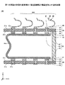
図11は、第1の実施の形態の変形例1に係る接続端子構造を例示する断面図である。図11を参照するに、第1の実施の形態の変形例1に係る接続端子構造10Aは、基板20が削除され、補強板25が設けられ、支持体55が支持体57に置換された点が、接続端子構造10(図3〜図6参照)と相違する。   FIG. 11 is a cross-sectional view illustrating a connection terminal structure according to Modification 1 of the first embodiment. Referring to FIG. 11, the connection terminal structure 10 </ b> A according to the first modification of the first embodiment is obtained by removing the substrate 20, providing the reinforcing plate 25, and replacing the support body 55 with the support body 57. However, it is different from the connection terminal structure 10 (see FIGS. 3 to 6).

接続端子構造10Aにおいて、補強板25は、例えば、絶縁性樹脂から形成された平板状の部材である。補強板25には、電極パッドや貫通配線等の導電部は形成されていない。補強板25の厚さは、例えば、数mm程度とすることができる。支持体57は、例えば、アルミニウム(Al)やステンレス(SUS)等の金属材料や、エポキシ樹脂等を主成分とする樹脂材料等により形成された箱状の部材(例えば、直方体のブロック)である。支持体57は、中空であってもよいし、そうでなくてもよい(図11の例では中空)。   In the connection terminal structure 10A, the reinforcing plate 25 is a flat plate member made of, for example, an insulating resin. The reinforcing plate 25 is not formed with conductive portions such as electrode pads and through wiring. The thickness of the reinforcing plate 25 can be set to about several mm, for example. The support 57 is a box-shaped member (for example, a rectangular parallelepiped block) formed of a metal material such as aluminum (Al) or stainless steel (SUS), a resin material mainly composed of an epoxy resin, or the like. . The support 57 may be hollow or not (hollow in the example of FIG. 11).

接続端子群30Aの各接続端子30は、接合部40を介して、フレキシブル基板50の基板本体51の一方の面51aの一端側に形成された各電極パッド52と電気的に接続されている。又、接続端子群30Bの各接続端子30は、フレキシブル基板50の基板本体51の一方の面51aの他端側に形成された各電極パッド53と電気的に接続されている。なお、各電極パッド52及び53は、接続端子30の位置に対応して例えばペリフェラル状やエリアアレイ状に配列されている。   Each connection terminal 30 of the connection terminal group 30 </ b> A is electrically connected to each electrode pad 52 formed on one end side of one surface 51 a of the substrate body 51 of the flexible substrate 50 through the joint portion 40. Each connection terminal 30 of the connection terminal group 30 </ b> B is electrically connected to each electrode pad 53 formed on the other end side of the one surface 51 a of the substrate body 51 of the flexible substrate 50. The electrode pads 52 and 53 are arranged in a peripheral shape or an area array shape, for example, corresponding to the position of the connection terminal 30.

フレキシブル基板50の基板本体51の他方の面51bの一端側は、一方の補強板25を介して、支持体57の上面に接合されている。フレキシブル基板50の基板本体51の他方の面51bの他端側は、他方の補強板25を介して、支持体57の下面に接合されている。つまり、支持体57は、一方の面51aを外側に向けて一方の補強板25と他方の補強板25とが対向するようにフレキシブル基板50を折り曲げた状態で、一方の補強板25及び他方の補強板25を支持している。フレキシブル基板50と補強板25、及び補強板25と支持体57とは、例えば、接着剤(図示せず)を介して接合できる。なお、フレキシブル基板50と補強板25、及び補強板25と支持体57とは、接着剤を用いずに、圧入やねじ止め等により固定しても構わない。   One end side of the other surface 51 b of the substrate body 51 of the flexible substrate 50 is joined to the upper surface of the support body 57 through one reinforcing plate 25. The other surface 51 b of the other surface 51 b of the substrate body 51 of the flexible substrate 50 is joined to the lower surface of the support 57 through the other reinforcing plate 25. That is, the support 57 is formed by bending the flexible substrate 50 so that the one reinforcing plate 25 and the other reinforcing plate 25 face each other with the one surface 51a facing outward. The reinforcing plate 25 is supported. The flexible substrate 50 and the reinforcing plate 25 and the reinforcing plate 25 and the support body 57 can be bonded to each other through an adhesive (not shown), for example. The flexible substrate 50 and the reinforcing plate 25, and the reinforcing plate 25 and the support body 57 may be fixed by press-fitting or screwing without using an adhesive.

フレキシブル基板50の電極パッド52が形成されている領域と電極パッド53が形成されている領域とを繋ぐ領域は、例えば、接着剤(図示せず)を介して、支持体57の外側面と接合されている。なお、フレキシブル基板50の基板本体51は、各補強板25よりも柔軟性が高いポリイミド樹脂や液晶ポリマ等の材料により形成されている。   The region connecting the region where the electrode pad 52 of the flexible substrate 50 is formed and the region where the electrode pad 53 is formed is bonded to the outer surface of the support 57 via, for example, an adhesive (not shown). Has been. The substrate body 51 of the flexible substrate 50 is formed of a material such as polyimide resin or liquid crystal polymer that is more flexible than the reinforcing plates 25.

なお、フレキシブル基板50に接合端子30を接合する際には、予めフレキシブル基板50の基板本体51の他方の面51bの一端側及び他端側に、それぞれ補強板25を接合しておく。   In addition, when joining the joining terminal 30 to the flexible substrate 50, the reinforcing plate 25 is joined to one end side and the other end side of the other surface 51b of the substrate body 51 of the flexible substrate 50 in advance.

このように、第1の実施の形態の変形例1によれば、第1の実施の形態と同様の効果を奏するが、更に、以下の効果を奏する。すなわち、第1の実施の形態に係る基板20に代えて、電極パッドや貫通配線等の導電部が形成されていない補強板25を用いることにより、補強板25の材料費や加工費が低減可能となり、接続端子構造10Aを接続端子構造10よりも低価格化できる。   As described above, according to the first modification of the first embodiment, the same effects as those of the first embodiment are obtained, but the following effects are further obtained. That is, instead of the substrate 20 according to the first embodiment, the material cost and the processing cost of the reinforcing plate 25 can be reduced by using the reinforcing plate 25 in which conductive portions such as electrode pads and through wirings are not formed. Thus, the connection terminal structure 10 </ b> A can be made cheaper than the connection terminal structure 10.

なお、第1の実施の形態の変形例1において、第1の実施の形態と同様に、支持体55を用いてもよい。   In the first modification of the first embodiment, the support body 55 may be used as in the first embodiment.

〈第1の実施の形態の変形例2〉
第1の実施の形態の変形例2では、支持体の一方の側のみに接続端子群を設ける例を示す。なお、第1の実施の形態の変形例2において、既に説明した実施の形態と同一構成部品についての説明は省略する。
<Modification 2 of the first embodiment>
The second modification of the first embodiment shows an example in which a connection terminal group is provided only on one side of the support. In the second modification of the first embodiment, the description of the same components as those of the already described embodiment is omitted.

図12は、第1の実施の形態の変形例2に係る接続端子構造を例示する断面図である。図12を参照するに、第1の実施の形態の変形例2に係る接続端子構造10Bは、接続端子群30B、及び他方の基板20と接続端子群30Bとを接合する接合部40が削除された点が、接続端子構造10(図3〜図6参照)と相違する。つまり、接続端子構造10Bでは、支持体55の一方の側に支持されている一方の基板20には接続端子群30Aが設けられているが、他方の側に支持されている他方の基板20には接続端子群が設けられていない。支持体55の他方の側には他方の基板20の電極パッド22が露出している。   FIG. 12 is a cross-sectional view illustrating a connection terminal structure according to Modification 2 of the first embodiment. Referring to FIG. 12, in connection terminal structure 10B according to Modification 2 of the first embodiment, connection terminal group 30B and joint 40 that joins the other substrate 20 and connection terminal group 30B are deleted. This is different from the connection terminal structure 10 (see FIGS. 3 to 6). That is, in the connection terminal structure 10B, the connection terminal group 30A is provided on one substrate 20 supported on one side of the support body 55, but the other substrate 20 supported on the other side is provided. There is no connection terminal group. The electrode pad 22 of the other substrate 20 is exposed on the other side of the support body 55.

接続端子構造10Bを用いると、例えば、他方の基板20の電極パッド22をはんだ等を介して被接続物の電極パッドに接合し、接続端子群30Aの各接続端子30の接続部32を他の被接続物の電極パッドに当接させ、他の被接続物を被接続物側に押圧することにより、被接続物を他の被接続物と電気的に接続することができる。なお、他方の基板20の電極パッド22上に予めはんだ等の接合部を形成しておいてもよい。   When the connection terminal structure 10B is used, for example, the electrode pad 22 of the other substrate 20 is joined to the electrode pad of the connected object via solder or the like, and the connection portion 32 of each connection terminal 30 of the connection terminal group 30A is connected to the other. The contacted object can be electrically connected to the other connected object by abutting the electrode pad of the connected object and pressing the other connected object toward the connected object side. Note that a joint such as solder may be formed in advance on the electrode pad 22 of the other substrate 20.

このように、第1の実施の形態の変形例2によれば、第1の実施の形態と同様の効果を奏するが、更に、以下の効果を奏する。すなわち、支持体55の一方の側のみに接続端子群30Aを設けることにより、接続端子30の必要数が減るため、接続端子30の材料費や加工費が低減可能となり、接続端子構造10Bを接続端子構造10よりも低価格化できる。一方の被接続物とは着脱可能な状態で接続する必要がない場合には、接続端子構造10Bのような構造とすることができる。   As described above, according to the second modification of the first embodiment, the same effects as those of the first embodiment are obtained, but the following effects are further obtained. That is, by providing the connection terminal group 30A only on one side of the support body 55, the necessary number of connection terminals 30 is reduced, so that the material cost and processing cost of the connection terminals 30 can be reduced, and the connection terminal structure 10B is connected. The price can be reduced as compared with the terminal structure 10. When it is not necessary to connect to one of the connected objects in a detachable state, the connection terminal structure 10B can be used.

〈第1の実施の形態の変形例3〉
第1の実施の形態の変形例3では、第1の実施の形態とは平面形状の異なる接続端子構造の例を示す。なお、第1の実施の形態の変形例3において、既に説明した実施の形態と同一構成部品についての説明は省略する。
<Modification 3 of the first embodiment>
Modification 3 of the first embodiment shows an example of a connection terminal structure having a different planar shape from that of the first embodiment. Note that in the third modification of the first embodiment, the description of the same components as those of the already described embodiment will be omitted.

図13は、第1の実施の形態の変形例3に係る接続端子構造を例示する断面図である。図14は、第1の実施の形態の変形例3に係る接続端子構造を例示する平面図である。図13及び図14を参照するに、第1の実施の形態の変形例3に係る接続端子構造10Cは、基板20が基板20Aに、接続端子群30Aが接続端子群30Cに、接続端子群30Bが接続端子群30Dに、フレキシブル基板50がフレキシブル基板50Aに置換された点が、接続端子構造10(図3〜図6参照)と相違する。   FIG. 13 is a cross-sectional view illustrating a connection terminal structure according to Modification 3 of the first embodiment. FIG. 14 is a plan view illustrating a connection terminal structure according to Modification 3 of the first embodiment. 13 and 14, the connection terminal structure 10C according to the third modification of the first embodiment includes a substrate 20 as the substrate 20A, a connection terminal group 30A as the connection terminal group 30C, and a connection terminal group 30B. Is different from the connection terminal structure 10 (see FIGS. 3 to 6) in that the connection terminal group 30D and the flexible substrate 50 are replaced with the flexible substrate 50A.

接続端子構造10Cにおいて、各基板20Aは、中央部近傍に開口部21yが形成されている基板本体21Aを有する。各基板本体21Aの開口部21yの周辺部には、電極パッド22、貫通配線24、及び電極パッド23が配置されている。各電極パッド22及び23は、接続端子30の位置に対応して例えばペリフェラル状に配列されている。   In the connection terminal structure 10C, each substrate 20A has a substrate body 21A in which an opening 21y is formed in the vicinity of the center. An electrode pad 22, a through wiring 24, and an electrode pad 23 are disposed around the opening 21y of each substrate body 21A. The electrode pads 22 and 23 are arranged in a peripheral shape, for example, corresponding to the position of the connection terminal 30.

接続端子群30Cにおいて、一方の基板20Aの領域Lに配列された接続端子30と、領域Rに配列された接続端子30とは、概ね対向している。接続端子群30Dにおいて、他方の基板20Aの領域Lに配列された接続端子30と、領域Rに配列された接続端子30とは、概ね対向している。このような配列により、接続端子30がZ方向に押圧されたときに、横方向(Z方向以外の方向)に生じる反力を低減できる。特に、接続端子30の数が多いときに有効である。但し、例えば接続端子30の数が比較的少ない場合のように、横方向(Z方向以外の方向)に生じる反力が問題にならない場合には、領域Lの接続端子30と領域Rの接続端子30とが同一方向を向くように配列しても構わない。   In the connection terminal group 30C, the connection terminals 30 arranged in the region L of one substrate 20A and the connection terminals 30 arranged in the region R are generally opposed to each other. In the connection terminal group 30D, the connection terminals 30 arranged in the region L of the other substrate 20A and the connection terminals 30 arranged in the region R are generally opposed to each other. With such an arrangement, when the connection terminal 30 is pressed in the Z direction, the reaction force generated in the lateral direction (direction other than the Z direction) can be reduced. This is particularly effective when the number of connection terminals 30 is large. However, when the reaction force generated in the lateral direction (direction other than the Z direction) is not a problem, for example, when the number of the connection terminals 30 is relatively small, the connection terminals 30 in the region L and the connection terminals in the region R are used. 30 may be arranged in the same direction.

平面視において、接続端子30は、接続端子30の配設方向Cに対して所定の角度θをなして傾くように配列されている。但し、本実施の形態では、領域Lの接続端子30と領域Rの接続端子30とが概ね対向しているため、領域Lの接続端子30と領域Rの接続端子30とは、傾く方向が異なっている。所定の角度θは、例えば、25〜35度程度とすることができる。 In plan view, the connection terminals 30 are arranged so as to be inclined at a predetermined angle θ 1 with respect to the arrangement direction C of the connection terminals 30. However, in the present embodiment, since the connection terminal 30 in the region L and the connection terminal 30 in the region R are generally opposed to each other, the connection terminal 30 in the region L and the connection terminal 30 in the region R are inclined in different directions. ing. The predetermined angle θ 1 can be set to about 25 to 35 degrees, for example.

なお、図14では、領域Lの接続端子30と領域Rの接続端子30とが配設方向Cに垂直な対称軸に対して線対称となるように配列されているが、これとは異なる配列としてもよい。例えば、領域Lの接続端子30を図14の位置から、配設方向Cに平行な対称軸に対して線対称となるような位置に変更してもよい。つまり、領域Lの接続端子30と領域Rの接続端子30とが、同一方向に傾くようにしてもよい。   In FIG. 14, the connection terminals 30 in the region L and the connection terminals 30 in the region R are arranged so as to be line symmetric with respect to an axis of symmetry perpendicular to the arrangement direction C. It is good. For example, the connection terminal 30 in the region L may be changed from the position in FIG. 14 to a position that is line symmetric with respect to an axis of symmetry parallel to the arrangement direction C. That is, the connection terminal 30 in the region L and the connection terminal 30 in the region R may be inclined in the same direction.

フレキシブル基板50Aは、一端側の中央部近傍に開口部51xが形成されており、他端側の中央部近傍に開口部51yが形成されている基板本体51Aを有する。基板本体51Aの開口部51x及び51yと、各基板本体21Aの開口部21yとは、平面視において略重複する位置に形成されている。つまり、接続端子構造10Cは、一方の基板20Aの電極パッド22側から他方の基板20Aの電極パッド22側に貫通する開口部を有する。なお、開口部51x及び51yは、開口部21yより大きくてもよい。   The flexible substrate 50A has a substrate body 51A in which an opening 51x is formed in the vicinity of the central portion on one end side, and an opening 51y is formed in the vicinity of the central portion on the other end side. The openings 51x and 51y of the substrate main body 51A and the openings 21y of the respective substrate main bodies 21A are formed at substantially overlapping positions in plan view. That is, the connection terminal structure 10C has an opening that penetrates from the electrode pad 22 side of one substrate 20A to the electrode pad 22 side of the other substrate 20A. Note that the openings 51x and 51y may be larger than the opening 21y.

開口部51xの周辺部には、接続端子群30Cの各接続端子30が接続される電極パッド23に対応する電極パッド52が配置されており、開口部51yの周辺部には、接続端子群30Dの各接続端子30が接続される電極パッド23に対応する電極パッド53が配置されている。   An electrode pad 52 corresponding to the electrode pad 23 to which each connection terminal 30 of the connection terminal group 30C is connected is disposed in the periphery of the opening 51x, and the connection terminal group 30D is disposed in the periphery of the opening 51y. The electrode pads 53 corresponding to the electrode pads 23 to which the connection terminals 30 are connected are arranged.

このように、第1の実施の形態の変形例3によれば、第1の実施の形態と同様の効果を奏するが、更に、以下の効果を奏する。すなわち、各基板20A及びフレキシブル基板50Aに開口部を設けることにより、被接続物を他の被接続物と電気的に接続する際に、被接続物又は他の被接続物の一方又は双方に実装された背の高い部品を逃げることができる。   As described above, according to the third modification of the first embodiment, the same effects as those of the first embodiment are obtained, but the following effects are further obtained. That is, by providing an opening in each substrate 20A and flexible substrate 50A, when the connection object is electrically connected to another connection object, it is mounted on one or both of the connection object and the other connection object. The escaped tall parts can escape.

〈第2の実施の形態〉
第2の実施の形態では、第1の実施の形態の変形例3に係る接続端子構造10Cを用いて半導体パッケージの電気的な検査を行う例を示す。なお、第2の実施の形態において、既に説明した実施の形態と同一構成部品についての説明は省略する。
<Second Embodiment>
In the second embodiment, an example in which an electrical inspection of a semiconductor package is performed using the connection terminal structure 10C according to the third modification of the first embodiment will be described. In the second embodiment, the description of the same components as those of the already described embodiments is omitted.

図15は、検査の対象となる半導体パッケージを例示する断面図(その1)である。図15を参照するに、半導体パッケージ100は、半導体パッケージ60B上に接合部43を介して半導体パッケージ60Aが積層された所謂POP構造(パッケージオンパッケージ構造)の半導体パッケージである。   FIG. 15 is a cross-sectional view (part 1) illustrating a semiconductor package to be inspected. Referring to FIG. 15, a semiconductor package 100 is a semiconductor package having a so-called POP structure (package-on-package structure) in which a semiconductor package 60A is stacked on a semiconductor package 60B via a joint 43.

半導体パッケージ60Aは、基板61と、半導体チップ62と、封止樹脂63と、電極パッド64とを有する所謂LGA(Land grid array)である。基板61は、例えば絶縁性樹脂を含む基板本体に絶縁層、配線パターン、貫通配線等(図示せず)が形成されたものである。基板61の一方の面にはシリコン等を含む半導体チップ62が実装され、他方の面には配線パターンの一部である電極パッド64が形成されている。半導体チップ62と電極パッド64とは、基板61に形成された貫通配線(図示せず)を介して電気的に接続されている。   The semiconductor package 60 </ b> A is a so-called LGA (Land grid array) having a substrate 61, a semiconductor chip 62, a sealing resin 63, and an electrode pad 64. The substrate 61 is obtained by forming an insulating layer, a wiring pattern, a through wiring, etc. (not shown) on a substrate body containing an insulating resin, for example. A semiconductor chip 62 containing silicon or the like is mounted on one surface of the substrate 61, and an electrode pad 64 that is a part of a wiring pattern is formed on the other surface. The semiconductor chip 62 and the electrode pad 64 are electrically connected via a through wiring (not shown) formed in the substrate 61.

電極パッド64の材料は、例えば、銅(Cu)等である。電極パッド64の厚さは、例えば、5〜10μm程度である。半導体チップ62は、例えばフリップチップ接続により基板61に搭載され、絶縁性樹脂からなる封止樹脂63により封止されている。なお、半導体チップ62の背面を露出するように封止樹脂63を設け、半導体チップ62の背面に例えば銅(Cu)等からなる放熱板を配置しても構わない。   The material of the electrode pad 64 is, for example, copper (Cu). The electrode pad 64 has a thickness of about 5 to 10 μm, for example. The semiconductor chip 62 is mounted on the substrate 61 by flip chip connection, for example, and is sealed with a sealing resin 63 made of an insulating resin. The sealing resin 63 may be provided so as to expose the back surface of the semiconductor chip 62, and a heat sink made of, for example, copper (Cu) may be disposed on the back surface of the semiconductor chip 62.

電極パッド64は、基板61の他方の面の中央部近傍を除く領域に、例えばペリフェラル状に配置されている。なお、接続信頼性を向上するために、電極パッド64の上面に無電解めっき法等により貴金属層を積層形成しても構わない。貴金属層としては、例えば、金(Au)層やパラジウム(Pd)層等の貴金属を含む層を用いることができる。金(Au)層の下層として、ニッケル(Ni)層やNi/Pd層(Ni層とPd層をこの順番で積層した金属層)等を形成しても構わない。   The electrode pad 64 is arranged in a peripheral shape, for example, in a region excluding the vicinity of the central portion of the other surface of the substrate 61. In order to improve connection reliability, a noble metal layer may be laminated on the upper surface of the electrode pad 64 by an electroless plating method or the like. As the noble metal layer, for example, a layer containing a noble metal such as a gold (Au) layer or a palladium (Pd) layer can be used. As a lower layer of the gold (Au) layer, a nickel (Ni) layer, a Ni / Pd layer (a metal layer in which a Ni layer and a Pd layer are stacked in this order), or the like may be formed.

半導体パッケージ60Bは、基板61と、半導体チップ62と、封止樹脂63と、電極パッド64と、電極パッド65とを有する所謂LGA(Land grid array)である。基板61、半導体チップ62、封止樹脂63、及び電極パッド64については半導体パッケージ60Aと同様であるため説明を省略する。電極パッド65は、基板61の一方の面の半導体チップ62の周辺領域に形成されている。電極パッド65の形成位置は、半導体パッケージ60Aの電極パッド64の形成位置に対応している。   The semiconductor package 60B is a so-called LGA (Land grid array) having a substrate 61, a semiconductor chip 62, a sealing resin 63, an electrode pad 64, and an electrode pad 65. Since the substrate 61, the semiconductor chip 62, the sealing resin 63, and the electrode pad 64 are the same as those of the semiconductor package 60A, description thereof is omitted. The electrode pad 65 is formed in the peripheral region of the semiconductor chip 62 on one surface of the substrate 61. The formation position of the electrode pad 65 corresponds to the formation position of the electrode pad 64 of the semiconductor package 60A.

電極パッド65は、半導体チップ62と電気的に接続されている。又、電極パッド65は、他方の面の電極パッド64と貫通配線(図示せず)を介して電気的に接続されている。電極パッド65の材料等は電極パッド64と同様とすることができる。なお、半導体パッケージ60Aと同様に、電極パッド65の上面に貴金属層を積層形成しても構わない。   The electrode pad 65 is electrically connected to the semiconductor chip 62. The electrode pad 65 is electrically connected to the electrode pad 64 on the other surface via a through wiring (not shown). The material or the like of the electrode pad 65 can be the same as that of the electrode pad 64. Note that a noble metal layer may be stacked on the upper surface of the electrode pad 65 in the same manner as the semiconductor package 60A.

半導体パッケージ60Bの電極パッド65と半導体パッケージ60Aの電極パッド64とは、接合部43を介して電気的に接続されている。接合部43の材料は、接合部40等と同様とすることができる。なお、半導体パッケージ60Bの半導体チップ62は、半導体パッケージ60Aの半導体チップ62と同一機能であっても構わないし、異なる機能を備えていても構わない。   The electrode pad 65 of the semiconductor package 60 </ b> B and the electrode pad 64 of the semiconductor package 60 </ b> A are electrically connected via the joint 43. The material of the joint portion 43 can be the same as that of the joint portion 40 and the like. Note that the semiconductor chip 62 of the semiconductor package 60B may have the same function as the semiconductor chip 62 of the semiconductor package 60A or may have a different function.

半導体パッケージ100の電気的な検査を実施する場合、図15に示す完成状態で検査してもよいが、半導体パッケージ60A及び60Bの何れか一方に不具合が検出された場合には半導体パッケージ100のリペアが必要となる。そこで、このような問題を避けるため、接続端子構造10Cを用いて、相互に接合する前の半導体パッケージ60A及び60Bを電気的に検査することが好ましい。以下に半導体パッケージ60A及び60Bを電気的に検査する際の接続例を示す。   When the electrical inspection of the semiconductor package 100 is performed, the inspection may be performed in the completed state shown in FIG. 15, but when a defect is detected in one of the semiconductor packages 60A and 60B, the repair of the semiconductor package 100 is performed Is required. Therefore, in order to avoid such a problem, it is preferable to electrically inspect the semiconductor packages 60A and 60B before being bonded to each other using the connection terminal structure 10C. A connection example when electrically inspecting the semiconductor packages 60A and 60B will be described below.

図16は、半導体パッケージを電気的に検査する際の接続例を示す断面図(その1)である。図16を参照するに、検査用基板70、第1の接続端子構造10C(便宜上、接続端子構造10Cとする)、半導体パッケージ60B、第2の接続端子構造10C(便宜上、接続端子構造10Cとする)、半導体パッケージ60Aが順次積層され、筐体80により保持されている。なお、接続端子構造10C、接続端子構造10C、及び筐体80は、本発明に係るソケットの代表的な一例である。 FIG. 16 is a cross-sectional view (part 1) illustrating a connection example when an electrical inspection of a semiconductor package is performed. Referring to FIG. 16, the test substrate 70, a first connecting terminal structure 10C (for convenience, the connection to the terminal structure 10C 1), the semiconductor package 60B, the second connecting terminal structure 10C (for convenience, the connection terminal structure 10C 2 ), The semiconductor packages 60 </ b> A are sequentially stacked and held by the housing 80. The connection terminal structure 10C 1 , the connection terminal structure 10C 2 , and the housing 80 are typical examples of the socket according to the present invention.

検査用基板70は、基板本体71に配線パターンの一部である電極パッド72等が設けられた基板であり、半導体検査システム(図示せず)と電気的に接続されている。検査用基板70は、半導体検査システム(図示せず)と半導体パッケージ60A及び60Bとの間で検査用の電気信号を入出力することができる。   The inspection substrate 70 is a substrate in which an electrode pad 72 which is a part of a wiring pattern is provided on a substrate body 71, and is electrically connected to a semiconductor inspection system (not shown). The inspection substrate 70 can input and output electrical signals for inspection between a semiconductor inspection system (not shown) and the semiconductor packages 60A and 60B.

筐体80は、枠部81と、蓋部82とを有する。枠部81は、中央に略矩形状の開口部を有する額縁状の部材に位置決め保持部83〜86を設けたものであり、剛性のある金属や樹脂等から形成されている。枠部81は、例えば、検査用基板70を貫通するボルトや接着剤等(図示せず)により、検査用基板70の上面に固着されている。   The housing 80 includes a frame portion 81 and a lid portion 82. The frame portion 81 is a frame-like member having a substantially rectangular opening at the center, and positioning holding portions 83 to 86 are provided, and is formed of a rigid metal or resin. The frame portion 81 is fixed to the upper surface of the inspection substrate 70 by, for example, a bolt or an adhesive (not shown) penetrating the inspection substrate 70.

枠部81は、接続端子構造10C、半導体パッケージ60B、接続端子構造10C、及び半導体パッケージ60Aの位置決め及び保持をし、それぞれを位置合わせする機能を有する。又、枠部81は、接続端子構造10C、半導体パッケージ60B、接続端子構造10C、及び半導体パッケージ60Aの相互の間隔が所定値以下になることを防止する機能を有する。 The frame portion 81 has a function of positioning and holding the connection terminal structure 10C 1 , the semiconductor package 60B, the connection terminal structure 10C 2 , and the semiconductor package 60A and aligning them. Further, the frame portion 81 has a function of preventing the mutual distance between the connection terminal structure 10C 1 , the semiconductor package 60B, the connection terminal structure 10C 2 , and the semiconductor package 60A from becoming a predetermined value or less.

位置決め保持部83は、面83aと面83bとを有する。面83aは、枠部81の上面81aよりも内側の、上面81aよりも一段下がった位置に、上面81aと略平行に額縁状に設けられた面である。面83bは、面83aと上面81aとの間に上面81aと略垂直に設けられた面であり、枠部81の内側面の一部である。   The positioning holding part 83 has a surface 83a and a surface 83b. The surface 83a is a surface provided in a frame shape substantially parallel to the upper surface 81a at a position inside the upper surface 81a of the frame portion 81 and a step below the upper surface 81a. The surface 83b is a surface provided substantially perpendicular to the upper surface 81a between the surface 83a and the upper surface 81a, and is a part of the inner surface of the frame portion 81.

面83aは、半導体パッケージ60Aの基板61の下面の外縁部と接している。面83bの形成する開口部の形状は、半導体パッケージ60Aの平面形状に合わせて矩形状とされている。又、面83bの形成する開口部の形状は、半導体パッケージ60Aの着脱を可能とするため、基板61の外形形状よりも若干大きくされている。面83bと基板61の側面とは、接していても構わないし、接続端子構造10Cの接続端子群30Cの各接続端子30の他端である接続部32と半導体パッケージ60Aの電極パッド64との間に位置ずれが生じない程度の隙間があっても構わない。 The surface 83a is in contact with the outer edge portion of the lower surface of the substrate 61 of the semiconductor package 60A. The shape of the opening formed by the surface 83b is rectangular according to the planar shape of the semiconductor package 60A. In addition, the shape of the opening formed by the surface 83b is slightly larger than the outer shape of the substrate 61 so that the semiconductor package 60A can be attached and detached. The side surface 83b and the substrate 61, in contact to may also be a connection terminal structure 10C 2 connecting terminal groups 30C and the electrode pads 64 of which is the other end connecting portion 32 and the semiconductor package 60A of the connecting terminals 30 There may be a gap that does not cause misalignment.

半導体パッケージ60Aは、位置決め保持部83により保持されるため、位置決め保持部83の面83aよりも接続端子構造10C側に押し込まれることはない。その結果、半導体パッケージ60Aが必要以上に接続端子構造10C側に押し込まれ、接続端子30が必要以上に変形して破損することを防止できる。 The semiconductor package 60A is to be held by the positioning holding unit 83, it will not be pushed into the connecting terminal structure 10C 2 side from the surface 83a of the positioning holding unit 83. As a result, the semiconductor package 60A is pushed into the connecting terminal structure 10C 2 side more than necessary, it is possible to prevent the connection terminal 30 from being damaged by deformation than necessary.

位置決め保持部84は、面84aと面84bとを有する。面84aは、面83aよりも内側の、面83aよりも一段下がった位置に、上面81aと略平行に額縁状に設けられた面である。面84bは、面84aと面83aとの間に面84aと略垂直に設けられた面であり、枠部81の内側面の一部である。   The positioning holding portion 84 has a surface 84a and a surface 84b. The surface 84a is a surface provided in a frame shape substantially parallel to the upper surface 81a at a position inside the surface 83a and one step lower than the surface 83a. The surface 84 b is a surface provided substantially perpendicular to the surface 84 a between the surface 84 a and the surface 83 a and is a part of the inner surface of the frame portion 81.

面84aは、接続端子構造10Cの下側の基板20の下面の外縁部と接している。面84bの形成する開口部の形状は、接続端子構造10Cの平面形状に合わせて矩形状とされている。又、面84bの形成する開口部の形状は、接続端子構造10Cの着脱を可能とするため、基板20及び支持体55の外形形状よりも若干大きくされている。面84bと基板20及び支持体55の側面とは、接していても構わないし、接続端子構造10Cの接続端子群30Dの各接続端子30の他端である接続部32と半導体パッケージ60Bの電極パッド65との間に位置ずれが生じない程度の隙間があっても構わない。 Surface 84a is in contact with the lower surface of the outer edge portion of the lower substrate 20 of the connecting terminal structure 10C 2. The shape of the opening formed by the surface 84b is a rectangular shape in accordance with the planar shape of the connection terminal structure 10C 2. The shape of the opening formed by the surface 84b in order to allow attachment and detachment of the connecting terminal structure 10C 2, and is slightly larger than the outer shape of the substrate 20 and the support 55. The side surface 84b and the substrate 20 and the support 55, to may be in contact, the electrode of which is the other end connecting portion 32 and the semiconductor package 60B of the connection terminals 30 of the connecting terminal groups 30D connecting terminal structure 10C 2 There may be a gap between the pads 65 so as not to cause misalignment.

接続端子構造10Cは、位置決め保持部84により保持されるため、位置決め保持部84の面84aよりも半導体パッケージ60B側に押し込まれることはない。その結果、接続端子構造10Cが必要以上に半導体パッケージ60B側に押し込まれ、接続端子30が必要以上に変形して破損することを防止できる。 Connecting terminal structure 10C 2 is to be held by the positioning holding unit 84 and will not be pushed into the semiconductor package 60B side from the surface 84a of the positioning holding unit 84. As a result, it is possible to prevent the connection terminal structure 10C 2 is pushed into the semiconductor package 60B side more than necessary, damaged and deformed in the connecting terminal 30 is more than necessary.

位置決め保持部85は、面85aと面85bとを有する。面85aは、面84aよりも内側の、面84aよりも一段下がった位置に、上面81aと略平行に額縁状に設けられた面である。面85bは、面85aと面84aとの間に面85aと略垂直に設けられた面であり、枠部81の内側面の一部である。   The positioning holding part 85 has a surface 85a and a surface 85b. The surface 85a is a surface provided in a frame shape substantially parallel to the upper surface 81a at a position inside the surface 84a and one step lower than the surface 84a. The surface 85 b is a surface provided substantially perpendicular to the surface 85 a between the surface 85 a and the surface 84 a and is a part of the inner surface of the frame portion 81.

面85aは、半導体パッケージ60Bの基板61の下面の外縁部と接している。面85bの形成する開口部の形状は、半導体パッケージ60Bの平面形状に合わせて矩形状とされている。又、面85bの形成する開口部の形状は、半導体パッケージ60Bの着脱を可能とするため、基板61の外形形状よりも若干大きくされている。面85bと基板61の側面とは、接していても構わないし、接続端子構造10Cの接続端子群30Dの各接続端子30の他端である接続部32と半導体パッケージ60Bの電極パッド65との間に位置ずれが生じず、接続端子構造10Cの接続端子群30Cの各接続端子30の他端である接続部32と半導体パッケージ60Bの電極パッド64との間に位置ずれが生じない程度の隙間があっても構わない。 The surface 85a is in contact with the outer edge portion of the lower surface of the substrate 61 of the semiconductor package 60B. The shape of the opening formed by the surface 85b is rectangular according to the planar shape of the semiconductor package 60B. In addition, the shape of the opening formed by the surface 85b is slightly larger than the outer shape of the substrate 61 so that the semiconductor package 60B can be attached and detached. The side surface 85b and the substrate 61, in contact to may also be a connection terminal structure 10C 2 connecting terminal groups 30D and the other end connecting portion 32 and the electrode pads 65 of the semiconductor package 60B is for the connecting terminals 30 positional deviation does not occur between the connection terminal structure 10C 1 connecting terminal groups 30C to the extent that positional deviation does not occur between the electrode pad 64 of which is the other end connecting portion 32 and the semiconductor package 60B of the connection terminals 30 It does not matter if there is a gap.

半導体パッケージ60Bは、位置決め保持部85により保持されるため、位置決め保持部85の面85aよりも接続端子構造10C側に押し込まれることはない。その結果、接続端子構造10Cが必要以上に検査用基板70側に押し込まれ、接続端子30が必要以上に変形して破損することを防止できる。 The semiconductor package 60B is to be held by the positioning holding unit 85, it will not be pushed into the connecting terminal structure 10C 1 side than the surface 85a of the positioning holding unit 85. As a result, the connection terminal structure 10C 1 is pushed into the testing board 70 side more than necessary, it is possible to prevent the connection terminal 30 from being damaged by deformation than necessary.

位置決め保持部86は、面86aと面86bとを有する。面86aは、面85aよりも内側の、面85aよりも一段下がった位置に、上面81aと略平行に額縁状に設けられた面である。面86bは、面86aと面85aとの間に面86aと略垂直に設けられた面であり、枠部81の内側面の一部である。   The positioning holding part 86 has a surface 86a and a surface 86b. The surface 86a is a surface provided in a frame shape substantially parallel to the upper surface 81a at a position inside the surface 85a and one step lower than the surface 85a. The surface 86 b is a surface provided substantially perpendicular to the surface 86 a between the surface 86 a and the surface 85 a and is a part of the inner surface of the frame portion 81.

面86aは、接続端子構造10Cの下側の基板20の下面の外縁部と接している。面86bの形成する開口部の形状は、接続端子構造10Cの平面形状に合わせて矩形状とされている。又、面86bの形成する開口部の形状は、接続端子構造10Cの着脱を可能とするため、基板20及び支持体55の外形形状よりも若干大きくされている。面86bと基板20及び支持体55の側面とは、接していても構わないし、接続端子構造10Cの接続端子群30Dの各接続端子30の他端である接続部32と検査用基板70の電極パッド72との間に位置ずれが生じない程度の隙間があっても構わない。 Surface 86a is in contact with the lower surface of the outer edge portion of the lower substrate 20 of the connecting terminal structure 10C 1. The shape of the opening formed by the surface 86b is a rectangular shape in accordance with the planar shape of the connection terminal structure 10C 1. The shape of the opening formed by the surface 86b in order to allow the detachable connection terminal structure 10C 1, and is slightly larger than the outer shape of the substrate 20 and the support 55. The side surface 86b and the substrate 20 and the support 55, in contact to may also be a connection terminal structure 10C 1 connecting terminal groups 30D of which is the other end connecting portion 32 and the testing board 70 of the connection terminals 30 There may be a gap between the electrode pads 72 so as not to cause a positional shift.

接続端子構造10Cは、位置決め保持部86により保持されるため、位置決め保持部86の面86aよりも検査用基板70側に押し込まれることはない。その結果、接続端子構造10Cが必要以上に検査用基板70側に押し込まれ、接続端子30が必要以上に変形して破損することを防止できる。 Since the connection terminal structure 10 </ b> C 1 is held by the positioning holding portion 86, the connecting terminal structure 10 </ b> C 1 is not pushed closer to the inspection substrate 70 side than the surface 86 a of the positioning holding portion 86. As a result, the connection terminal structure 10C 1 is pushed into the testing board 70 side more than necessary, it is possible to prevent the connection terminal 30 from being damaged by deformation than necessary.

蓋部82は、例えば金属や樹脂等で形成される平面形状が略矩形状や略額縁状の部材である。蓋部82は、例えば枠部81の上面81aの一端側に回動可能に取り付けられており、他端側にロック機構を有する。   The lid portion 82 is a member having a substantially rectangular shape or a substantially frame shape in a planar shape formed of, for example, metal or resin. The lid portion 82 is rotatably attached to one end side of the upper surface 81a of the frame portion 81, for example, and has a lock mechanism on the other end side.

図16に示す状態にするためには、まず、他端側が枠部81の上面81aから離れる方向に蓋部82を回動させて、枠部81内に半導体パッケージ60A等を配置可能な状態とする。そして、枠部81内に、検査用基板70側から、接続端子構造10C、半導体パッケージ60B、接続端子構造10C、半導体パッケージ60Aを順次配置する。そして、他端側が枠部81の上面81aに近づく方向に蓋部82を回動させて、蓋部82の他端側が枠部81の上面81aと接するように固定する(ロックする)。これにより、蓋部82が接続端子構造10C、半導体パッケージ60B、接続端子構造10C、半導体パッケージ60Aを検査用基板70側に押し込み、それぞれが検査用基板70側に移動する。 In order to obtain the state shown in FIG. 16, first, the lid portion 82 is rotated in a direction in which the other end side is separated from the upper surface 81 a of the frame portion 81, so that the semiconductor package 60 </ b> A and the like can be disposed in the frame portion 81. To do. Then, the connection terminal structure 10C 1 , the semiconductor package 60B, the connection terminal structure 10C 2 , and the semiconductor package 60A are sequentially arranged in the frame portion 81 from the inspection substrate 70 side. Then, the lid 82 is rotated in a direction in which the other end approaches the upper surface 81a of the frame 81, and is fixed (locked) so that the other end of the lid 82 contacts the upper surface 81a of the frame 81. As a result, the lid 82 pushes the connection terminal structure 10C 1 , the semiconductor package 60B, the connection terminal structure 10C 2 , and the semiconductor package 60A toward the inspection substrate 70, and each moves toward the inspection substrate 70.

より詳しくは、接続端子構造10Cの接続端子群30Dの各接続端子30は押圧され厚さ方向に縮んで所定のばね圧が生じ、各接続端子30の接続部32は検査用基板70の各電極パッド72と当接する。又、接続端子構造10Cの接続端子群30Cの各接続端子30は押圧され厚さ方向に縮んで所定のばね圧が生じ、各接続端子30の接続部32は半導体パッケージ60Bの各電極パッド64と当接する。 More specifically, the connection terminals 30 of the connecting terminal groups 30D connecting terminal structure 10C 1 is squashed occur predetermined spring pressure pressed thickness direction, the connecting portion 32 of the connection terminals 30 each of the testing substrate 70 It abuts on the electrode pad 72. Further, the connection terminal connecting terminals 30 of the connection terminals 30C structure 10C 1 is squashed occur predetermined spring pressure pressed thickness direction, each of the electrode pads 64 of the connecting portion 32 is a semiconductor package 60B of the connection terminals 30 Abut.

同様に、接続端子構造10Cの接続端子群30Dの各接続端子30は押圧され厚さ方向に縮んで所定のばね圧が生じ、各接続端子30の接続部32は半導体パッケージ60Bの各電極パッド65と当接する。又、接続端子構造10Cの接続端子群30Cの各接続端子30は押圧され厚さ方向に縮んで所定のばね圧が生じ、各接続端子30の接続部32は半導体パッケージ60Aの各電極パッド64と当接する。 Similarly, the connection terminal structure 10C each connecting terminal 30 of the second connection terminal group 30D occurs a predetermined spring pressure shrinks the pressed thickness direction, the connecting portion 32 of the connection terminals 30 are electrode pads of the semiconductor package 60B 65 abuts. The connection terminal structure 10C each connecting terminal 30 of the second connection terminal group 30C is pressed cause a predetermined spring pressure shrinks in the thickness direction, each of the electrode pads 64 of the connecting portion 32 is a semiconductor package 60A of the connecting terminals 30 Abut.

その結果、半導体パッケージ60Bは接続端子構造10Cを介して半導体パッケージ60Aと電気的に接続され、図15に示す半導体パッケージ100と同様な接続状態が実現できる。又、半導体パッケージ60B、接続端子構造10C、半導体パッケージ60Aの積層体(半導体パッケージ100に相当する部分)は、接続端子構造10Cを介して検査用基板70と電気的に接続される。つまり、半導体パッケージ60B、接続端子構造10C、半導体パッケージ60Aの積層体(半導体パッケージ100に相当する部分)の電気的な検査が可能な状態となる。検査終了後、蓋部82のロックを解除することにより、半導体パッケージ60A及び60B並びに接続端子構造10C及び10Cは枠部81から取り外すことができる。 As a result, the semiconductor package 60B is connected to the semiconductor package 60A electrically through a connecting terminal structure 10C 2, it can be realized similar to a connected state with the semiconductor package 100 shown in FIG. 15. Further, the semiconductor package 60B, the connection terminal structure 10C 2, the laminate of the semiconductor package 60A (the portion corresponding to the semiconductor package 100) via a connecting terminal structure 10C 1 is connected inspection board 70 and electrically. That is, the semiconductor package 60B, the connection terminal structure 10C 2 , and the stacked body of the semiconductor package 60A (part corresponding to the semiconductor package 100) can be electrically inspected. After completion of the inspection, by releasing the locking of the lid 82, the semiconductor package 60A and 60B and the connecting terminal structure 10C 1 and 10C 2 can be detached from the frame portion 81.

なお、蓋部82は、枠部81とは別体でも構わない。この場合には、例えば、半導体パッケージ60A等を蓋部82により上側から押圧した状態で、蓋部82が枠部81に固定可能な構造であれば良い。   The lid portion 82 may be a separate body from the frame portion 81. In this case, for example, the lid 82 may be fixed to the frame 81 in a state where the semiconductor package 60 </ b> A or the like is pressed from above by the lid 82.

このように、第2の実施の形態では、半導体パッケージ100を構成する半導体パッケージ60Aと半導体パッケージ60Bとを接続端子構造10Cを介して電気的に接続し、更にこれらを接続端子構造10Cを介して検査用基板70と電気的に接続する。これにより、相互に接合する前の半導体パッケージ60A及び60Bを一時的に接続し、半導体パッケージ100としての電気的な検査を実現できる。その結果、半導体パッケージ60A及び60Bの何れもが良品であると判定された場合のみ両者を相互に接合して半導体パッケージ100を完成させることが可能となり、不要なリペアを回避できる。 Thus, in the second embodiment, and electrically connecting the semiconductor package 60A and the semiconductor package 60B of the semiconductor package 100 via a connecting terminal structure 10C 2, further connection terminal structure 10C 1 these And is electrically connected to the inspection substrate 70. Thereby, the semiconductor packages 60A and 60B before being bonded to each other can be temporarily connected, and an electrical inspection as the semiconductor package 100 can be realized. As a result, only when it is determined that both of the semiconductor packages 60A and 60B are non-defective products, it is possible to complete the semiconductor package 100 by bonding them together, and unnecessary repair can be avoided.

なお、半導体パッケージ60A及び60Bのように、被接続物が背の高い部品を含んでいない場合には、接続端子構造10Cに代えて、中央部近傍に開口部を有さない接続端子構造10や10Aを用いることもできる。   In addition, when the connected object does not include a tall component like the semiconductor packages 60A and 60B, instead of the connection terminal structure 10C, the connection terminal structure 10 having no opening near the center portion or 10A can also be used.

〈第2の実施の形態の変形例1〉
第2の実施の形態の変形例1では、第1の実施の形態の変形例3に係る接続端子構造10Cを用いて、第2の実施の形態とは異なる半導体パッケージの電気的な検査を行う例を示す。なお、第2の実施の形態の変形例1において、既に説明した実施の形態と同一構成部品についての説明は省略する。
<Modification Example 1 of Second Embodiment>
In the first modification of the second embodiment, an electrical inspection of a semiconductor package different from the second embodiment is performed using the connection terminal structure 10C according to the third modification of the first embodiment. An example is shown. In the first modification of the second embodiment, the description of the same components as those of the already described embodiment is omitted.

図17は、検査の対象となる半導体パッケージを例示する断面図(その2)である。図17を参照するに、半導体パッケージ100Aは、半導体パッケージ60D上に接合部44を介して半導体パッケージ60Cが積層された所謂POP構造(パッケージオンパッケージ構造)の半導体パッケージである。   FIG. 17 is a cross-sectional view (part 2) illustrating a semiconductor package to be inspected. Referring to FIG. 17, a semiconductor package 100A is a semiconductor package having a so-called POP structure (package-on-package structure) in which a semiconductor package 60C is stacked on a semiconductor package 60D via a junction 44.

半導体パッケージ60Cは、基板61と、半導体チップ62と、封止樹脂63と、電極パッド64と、半導体チップ67と、封止樹脂68と、電子部品69とを有する所謂LGA(Land grid array)である。基板61、半導体チップ62、封止樹脂63、及び電極パッド64については半導体パッケージ60Aと同様であるため説明を省略する。半導体パッケージ60Cは、半導体パッケージ60Aの基板61の他方の面にシリコン等を含む半導体チップ67及び電子部品69が実装され、半導体チップ67が封止樹脂68で封止された構造を有する。電子部品69は、例えば、キャパシタ、インダクタ、抵抗等であり、封止樹脂68に封止された半導体チップ67よりも背が高い。   The semiconductor package 60C is a so-called LGA (Land grid array) having a substrate 61, a semiconductor chip 62, a sealing resin 63, an electrode pad 64, a semiconductor chip 67, a sealing resin 68, and an electronic component 69. is there. Since the substrate 61, the semiconductor chip 62, the sealing resin 63, and the electrode pad 64 are the same as those of the semiconductor package 60A, description thereof is omitted. The semiconductor package 60C has a structure in which a semiconductor chip 67 containing silicon or the like and an electronic component 69 are mounted on the other surface of the substrate 61 of the semiconductor package 60A, and the semiconductor chip 67 is sealed with a sealing resin 68. The electronic component 69 is, for example, a capacitor, an inductor, a resistor, or the like, and is taller than the semiconductor chip 67 sealed with the sealing resin 68.

半導体パッケージ60Dは、基板61と、半導体チップ62と、封止樹脂63と、電極パッド64と、電極パッド65と、半導体チップ67と、封止樹脂68と、電子部品69とを有する所謂LGA(Land grid array)である。基板61、半導体チップ62、封止樹脂63、電極パッド64、及び電極パッド65については半導体パッケージ60Bと同様であるため説明を省略する。半導体パッケージ60Dは、半導体パッケージ60Bの基板61の他方の面にシリコン等を含む半導体チップ67及び電子部品69が実装され、半導体チップ67が封止樹脂68で封止された構造を有する。なお、半導体パッケージ60Dの電極パッド64には接合部44(バンプ)が形成されているが、接合部44(バンプ)は形成しなくてもよい。その場合には、接合部44(バンプ)は半導体パッケージ60Dが接続される実装基板等の側に形成される。   The semiconductor package 60D is a so-called LGA (LGA) having a substrate 61, a semiconductor chip 62, a sealing resin 63, an electrode pad 64, an electrode pad 65, a semiconductor chip 67, a sealing resin 68, and an electronic component 69. Land grid array). Since the substrate 61, the semiconductor chip 62, the sealing resin 63, the electrode pad 64, and the electrode pad 65 are the same as those of the semiconductor package 60B, description thereof is omitted. The semiconductor package 60D has a structure in which a semiconductor chip 67 containing silicon or the like and an electronic component 69 are mounted on the other surface of the substrate 61 of the semiconductor package 60B, and the semiconductor chip 67 is sealed with a sealing resin 68. In addition, although the joining part 44 (bump) is formed in the electrode pad 64 of the semiconductor package 60D, the joining part 44 (bump) may not be formed. In that case, the joint portion 44 (bump) is formed on the side of the mounting substrate or the like to which the semiconductor package 60D is connected.

半導体パッケージ60Dの電極パッド65と半導体パッケージ60Cの電極パッド64とは、接合部44を介して電気的に接続されている。接合部44としては、例えば、銅(Cu)を主成分とするコア部44aの周囲をはんだ44bで被覆した所謂銅コアはんだボール等を用いることができる。なお、半導体パッケージ60Dの半導体チップ67は、半導体パッケージ60Cの半導体チップ67と同一機能であっても構わないし、異なる機能を備えていても構わない。   The electrode pad 65 of the semiconductor package 60D and the electrode pad 64 of the semiconductor package 60C are electrically connected through the joint portion 44. As the joining portion 44, for example, a so-called copper core solder ball in which the periphery of a core portion 44a mainly composed of copper (Cu) is covered with solder 44b can be used. Note that the semiconductor chip 67 of the semiconductor package 60D may have the same function as the semiconductor chip 67 of the semiconductor package 60C, or may have a different function.

半導体パッケージ100Aの電気的な検査を実施する場合、第2の実施の形態と同様に、接続端子構造10Cを用いて、相互に接合する前の半導体パッケージ60C及び60Dを電気的に検査することが好ましい。以下に半導体パッケージ60C及び60Dを電気的に検査する際の接続例を示す。   When the electrical inspection of the semiconductor package 100A is performed, the semiconductor packages 60C and 60D before being bonded to each other can be electrically inspected using the connection terminal structure 10C, as in the second embodiment. preferable. A connection example when electrically inspecting the semiconductor packages 60C and 60D will be described below.

図18は、半導体パッケージを電気的に検査する際の接続例を示す断面図(その2)である。図18を参照するに、検査用基板70、接続端子構造10C、半導体パッケージ60D、接続端子構造10C、半導体パッケージ60Cが順次積層され、筐体80により保持されている。換言すれば、図18に示す構造体は、図16において、半導体パッケージ60Aを半導体パッケージ60Cに、半導体パッケージ60Bを半導体パッケージ60Dに置換したものである。なお、接続端子構造10C、接続端子構造10C、及び筐体80は、本発明に係るソケットの代表的な一例である。 FIG. 18 is a cross-sectional view (part 2) illustrating a connection example when the semiconductor package is electrically inspected. Referring to FIG. 18, the inspection substrate 70, the connection terminal structure 10 </ b > C 1 , the semiconductor package 60 </ b > D, the connection terminal structure 10 </ b > C 2 , and the semiconductor package 60 </ b > C are sequentially stacked and held by the housing 80. In other words, the structure shown in FIG. 18 is obtained by replacing the semiconductor package 60A with the semiconductor package 60C and the semiconductor package 60B with the semiconductor package 60D in FIG. The connection terminal structure 10C 1 , the connection terminal structure 10C 2 , and the housing 80 are typical examples of the socket according to the present invention.

第2の実施の形態と同様にして、半導体パッケージ60Dは接続端子構造10Cを介して半導体パッケージ60Cと電気的に接続され、図17に示す半導体パッケージ100Aと同様な接続状態が実現できる。又、半導体パッケージ60D、接続端子構造10C、半導体パッケージ60Cの積層体(半導体パッケージ100Aに相当する部分)は、接続端子構造10Cを介して検査用基板70と電気的に接続される。つまり、半導体パッケージ60D、接続端子構造10C、半導体パッケージ60Cの積層体(半導体パッケージ100Aに相当する部分)の電気的な検査が可能な状態となる。 In the same manner as in the second embodiment, the semiconductor package 60D is connected semiconductor package 60C and electrically through a connecting terminal structure 10C 2, it can be realized similar to the connection state and the semiconductor package 100A shown in FIG. 17. The semiconductor package 60D, connecting terminal structure 10C 2, the laminate of the semiconductor package 60C (portion corresponding to the semiconductor package 100A), via a connecting terminal structure 10C 1 is connected inspection board 70 and electrically. That is, the semiconductor package 60D, the connection terminal structure 10C 2 , and the stacked body of the semiconductor package 60C (part corresponding to the semiconductor package 100A) can be electrically inspected.

このように、第2の実施の形態の変形例1では、第2の実施の形態と同様の効果を奏するが、更に、以下の効果を奏する。すなわち、半導体パッケージ60Cや60Dに電子部品69のような背の高い部品が実装されていても、電子部品69を接続端子構造10C及び10Cの中央部近傍に形成された開口部内に配置することにより、半導体パッケージ60Cと半導体パッケージ60Dとを電気的に接続することが可能となる。 As described above, the first modification of the second embodiment has the same effects as those of the second embodiment, but also has the following effects. In other words, be tall components mounted such as a semiconductor package 60C and 60D to the electronic component 69 is placed in the electronic component 69 the connection terminal structure 10C 1 and 10C 2 of the central portion formed opening in the vicinity of As a result, the semiconductor package 60C and the semiconductor package 60D can be electrically connected.

〈第2の実施の形態の変形例2〉
第2の実施の形態の変形例2では、第1の実施の形態の変形例3に係る接続端子構造10Cを用いて、第2の実施の形態及びその変形例1とは異なる半導体パッケージの電気的な検査を行う例を示す。なお、第2の実施の形態の変形例2において、既に説明した実施の形態と同一構成部品についての説明は省略する。
<Modification 2 of the second embodiment>
In the second modification of the second embodiment, the connection terminal structure 10C according to the third modification of the first embodiment is used, and the electricity of the semiconductor package different from that of the second embodiment and the first modification thereof is used. An example of performing a typical inspection is shown. In the second modification of the second embodiment, the description of the same components as those of the already described embodiment is omitted.

図19は、検査の対象となる半導体パッケージを例示する断面図(その3)である。図19を参照するに、半導体パッケージ100Bは、半導体パッケージ60E上に中継基板90を介して半導体パッケージ60Aが積層された所謂POP構造(パッケージオンパッケージ構造)の半導体パッケージである。   FIG. 19 is a cross-sectional view (part 3) illustrating the semiconductor package to be inspected. Referring to FIG. 19, the semiconductor package 100B is a semiconductor package having a so-called POP structure (package on package structure) in which a semiconductor package 60A is stacked on a semiconductor package 60E via a relay substrate 90.

半導体パッケージ60Eは、基板61と、積層された複数の半導体チップ62と、封止樹脂63と、電極パッド64と、電極パッド65とを有する所謂LGA(Land grid array)である。基板61、封止樹脂63、電極パッド64、及び電極パッド65については半導体パッケージ60Bと同様であるため説明を省略する。各半導体チップ62には貫通電極が形成されており、積層された複数の半導体チップ62が貫通電極により相互に接続されている。   The semiconductor package 60E is a so-called LGA (Land grid array) having a substrate 61, a plurality of stacked semiconductor chips 62, a sealing resin 63, an electrode pad 64, and an electrode pad 65. Since the substrate 61, the sealing resin 63, the electrode pad 64, and the electrode pad 65 are the same as those of the semiconductor package 60B, description thereof is omitted. Each semiconductor chip 62 has a through electrode, and a plurality of stacked semiconductor chips 62 are connected to each other through the through electrode.

半導体パッケージ60Eの電極パッド65と半導体パッケージ60Aの電極パッド64とは、中継基板90を介して電気的に接続されている。中継基板90は、基板本体91と、基板本体91の一方の面に形成された複数の電極パッド92と、電極パッド92上に形成された接合部94と、他方の面に形成された複数の電極パッド93と、電極パッド93上に形成された接合部95とを有する。各電極パッド92と各電極パッド93とは、基板本体91を貫通する貫通配線(図示せず)により電気的に接続されている。中継基板90の基板本体91、電極パッド92及び93の材料等は、基板20の基板本体21、電極パッド22及び23と同様とすることができる。中継基板90の接合部94及び95の材料等は、接合部40等と同様とすることができる。なお、半導体パッケージ60Eの半導体チップ62は、半導体パッケージ60Aの半導体チップ62と同一機能であっても構わないし、異なる機能を備えていても構わない。   The electrode pad 65 of the semiconductor package 60E and the electrode pad 64 of the semiconductor package 60A are electrically connected via the relay substrate 90. The relay substrate 90 includes a substrate body 91, a plurality of electrode pads 92 formed on one surface of the substrate body 91, a joint portion 94 formed on the electrode pad 92, and a plurality of electrodes formed on the other surface. The electrode pad 93 and a joint portion 95 formed on the electrode pad 93 are included. Each electrode pad 92 and each electrode pad 93 are electrically connected by a through wiring (not shown) penetrating the substrate body 91. The material of the substrate body 91 and the electrode pads 92 and 93 of the relay substrate 90 can be the same as that of the substrate body 21 and the electrode pads 22 and 23 of the substrate 20. The materials and the like of the joint portions 94 and 95 of the relay substrate 90 can be the same as those of the joint portion 40 and the like. Note that the semiconductor chip 62 of the semiconductor package 60E may have the same function as the semiconductor chip 62 of the semiconductor package 60A or may have a different function.

半導体パッケージ100Bの電気的な検査を実施する場合、第2の実施の形態と同様に、接続端子構造10Cを用いて、相互に接合する前の半導体パッケージ60A及び60Eを電気的に検査することが好ましい。以下に半導体パッケージ60A及び60Eを電気的に検査する際の接続例を示す。   When the electrical inspection of the semiconductor package 100B is performed, the semiconductor packages 60A and 60E before being bonded to each other can be electrically inspected using the connection terminal structure 10C, as in the second embodiment. preferable. A connection example when electrically inspecting the semiconductor packages 60A and 60E will be described below.

図20は、半導体パッケージを電気的に検査する際の接続例を示す断面図(その3)である。図20を参照するに、検査用基板70、接続端子構造10C、半導体パッケージ60E、接続端子構造10C、半導体パッケージ60Aが順次積層され、筐体80により保持されている。換言すれば、図20に示す構造体は、図16において、半導体パッケージ60Bを半導体パッケージ60Eに置換したものである。なお、接続端子構造10C、接続端子構造10C、及び筐体80は、本発明に係るソケットの代表的な一例である。 FIG. 20 is a cross-sectional view (part 3) illustrating a connection example when the semiconductor package is electrically inspected. Referring to FIG. 20, the test substrate 70, the connection terminal structure 10 </ b > C 1 , the semiconductor package 60 </ b > E, the connection terminal structure 10 </ b > C 2 , and the semiconductor package 60 </ b > A are sequentially stacked and held by the housing 80. In other words, the structure shown in FIG. 20 is obtained by replacing the semiconductor package 60B with the semiconductor package 60E in FIG. The connection terminal structure 10C 1 , the connection terminal structure 10C 2 , and the housing 80 are typical examples of the socket according to the present invention.

第2の実施の形態と同様にして、半導体パッケージ60Eは接続端子構造10Cを介して半導体パッケージ60Aと電気的に接続され、図19に示す半導体パッケージ100Bと同様な接続状態が実現できる。又、半導体パッケージ60E、接続端子構造10C、半導体パッケージ60Aの積層体(半導体パッケージ100Bに相当する部分)は、接続端子構造10Cを介して検査用基板70と電気的に接続される。つまり、半導体パッケージ60E、接続端子構造10C、半導体パッケージ60Aの積層体(半導体パッケージ100Bに相当する部分)の電気的な検査が可能な状態となる。 In the same manner as in the second embodiment, the semiconductor package 60E is connected to the semiconductor package 60A electrically through a connecting terminal structure 10C 2, it can be realized similar to the connection state and the semiconductor package 100B shown in FIG. 19. The semiconductor package 60E, the connection terminal structure 10C 2, the laminate of the semiconductor package 60A (the portion corresponding to the semiconductor package 100B) via the connecting terminal structure 10C 1 is connected inspection board 70 and electrically. That is, the semiconductor package 60E, the connection terminal structure 10C 2 , and the stacked body of the semiconductor package 60A (part corresponding to the semiconductor package 100B) can be electrically inspected.

このように、第2の実施の形態の変形例2では、第2の実施の形態と同様の効果を奏するが、更に、以下の効果を奏する。すなわち、半導体パッケージ60Eのように複数の半導体チップ62が積層されて背が高くなっても、積層された半導体チップ62を接続端子構造10Cの中央部近傍に形成された開口部内に配置することにより、半導体パッケージ60Eと半導体パッケージ60Aとを電気的に接続することが可能となる。 As described above, Modification 2 of the second embodiment has the same effects as those of the second embodiment, but also has the following effects. In other words, a plurality of semiconductor chips 62 as semiconductor package 60E is also made by stacking tall, to place a semiconductor chip 62 stacked on the connection terminal structure 10C 2 of the central portion formed opening in the vicinity of Thus, the semiconductor package 60E and the semiconductor package 60A can be electrically connected.

なお、第2の実施の形態及びその変形例1、2では、接続端子構造10Cの支持体55を同一高さとして図示しているが、本発明に係る接続端子構造では支持体の高さを容易に変更できるため、支持体の高さが異なる複数の接続端子構造を準備し、被接続物の高さに応じて適宜使い分けるようにすることができる。つまり、多様な高さを有する多品種の接続端子構造やソケットを容易に実現できる。   In the second embodiment and its modifications 1 and 2, the support body 55 of the connection terminal structure 10C is illustrated as having the same height. However, in the connection terminal structure according to the present invention, the height of the support body is set. Since it can be easily changed, a plurality of connection terminal structures having different support body heights can be prepared and used appropriately according to the height of the connected object. That is, various types of connection terminal structures and sockets having various heights can be easily realized.

〈第3の実施の形態〉
第3の実施の形態では、第1の実施の形態の変形例3に係る接続端子構造10Cを構成要素とする電子部品パッケージの例を示す。なお、第3の実施の形態において、既に説明した実施の形態と同一構成部品についての説明は省略する。
<Third Embodiment>
In the third embodiment, an example of an electronic component package including the connection terminal structure 10C according to the third modification of the first embodiment as a constituent element is shown. In the third embodiment, the description of the same components as those of the already described embodiments is omitted.

図21は、第3の実施の形態に係る電子部品パッケージを例示する断面図である。図21を参照するに、電子部品パッケージ100Cは、半導体パッケージ60E上に接続端子構造10Cを介して半導体パッケージ60Aが積層され、筐体80Aにより保持されている所謂POP構造(パッケージオンパッケージ構造)の半導体パッケージである。なお、本発明に係る電子部品パッケージは、半導体チップを含む構造(半導体パッケージ)でもよいし、例えば、半導体チップを含まない配線基板同士を接続する構造であってもよい。   FIG. 21 is a cross-sectional view illustrating an electronic component package according to the third embodiment. Referring to FIG. 21, an electronic component package 100C has a so-called POP structure (package-on-package structure) in which a semiconductor package 60A is stacked on a semiconductor package 60E via a connection terminal structure 10C and is held by a housing 80A. It is a semiconductor package. The electronic component package according to the present invention may have a structure including a semiconductor chip (semiconductor package), or may have a structure in which wiring boards that do not include a semiconductor chip are connected to each other.

筐体80Aは、枠部87と、蓋部88とを有する。枠部87は、中央に略矩形状の開口部を有する額縁状の部材に枠部81と同様の位置決め保持部83及び84を設けたものであり、剛性のある金属や樹脂等から形成されている。枠部87の底面は、例えば、半導体パッケージ60Eの基板61の一方の面の外縁部に接着剤等により固着されている。枠部87は、ねじ等を用いて半導体パッケージ60Eの基板61と機械的に固着しても構わない。   The housing 80 </ b> A includes a frame portion 87 and a lid portion 88. The frame portion 87 is a frame-shaped member having a substantially rectangular opening at the center and is provided with positioning holding portions 83 and 84 similar to the frame portion 81, and is formed of a rigid metal or resin. Yes. For example, the bottom surface of the frame portion 87 is fixed to an outer edge portion of one surface of the substrate 61 of the semiconductor package 60E with an adhesive or the like. The frame portion 87 may be mechanically fixed to the substrate 61 of the semiconductor package 60E using screws or the like.

枠部87は、半導体パッケージ60E、接続端子構造10C、及び半導体パッケージ60Aの位置決め及び保持をし、それぞれを位置合わせする機能を有する。又、枠部87は、半導体パッケージ60E、接続端子構造10C、及び半導体パッケージ60Aの相互の間隔が所定値以下になることを防止する機能を有する。   The frame portion 87 has a function of positioning and holding the semiconductor package 60E, the connection terminal structure 10C, and the semiconductor package 60A and aligning them. The frame portion 87 has a function of preventing the distance between the semiconductor package 60E, the connection terminal structure 10C, and the semiconductor package 60A from becoming a predetermined value or less.

蓋部88は、枠部87とは別体である。蓋部88は、接続端子構造10C及び半導体パッケージ60Aが枠部87内の半導体パッケージ60E上に順次配置された後、これらを上側から押圧した状態で、枠部87の上面87aに固定されている。但し、蓋部88を枠部87の上面87aに固定可能な構造とすることに代えて、蓋部88を蓋部82と同様にロック機構を有する回動可能な構造としても構わない。このような構造とすると、電子部品パッケージ100Cを容易にリペアすることが可能となる。   The lid part 88 is a separate body from the frame part 87. The lid 88 is fixed to the upper surface 87a of the frame 87 in a state where the connection terminal structure 10C and the semiconductor package 60A are sequentially arranged on the semiconductor package 60E in the frame 87 and pressed from above. . However, in place of the lid 88 having a structure that can be fixed to the upper surface 87a of the frame 87, the lid 88 may have a rotatable structure having a lock mechanism in the same manner as the lid 82. With such a structure, the electronic component package 100C can be easily repaired.

接続端子構造10Cの接続端子群30Dの各接続端子30は押圧され厚さ方向に縮んで所定のばね圧が生じ、各接続端子30の接続部32は半導体パッケージ60Eの各電極パッド65と当接している。又、接続端子構造10Cの接続端子群30Cの各接続端子30は押圧され厚さ方向に縮んで所定のばね圧が生じ、各接続端子30の接続部32は半導体パッケージ60Aの各電極パッド64と当接している。このように、半導体パッケージ60Eは接続端子構造10Cを介して半導体パッケージ60Aと電気的に接続されている。   Each connection terminal 30 of the connection terminal group 30D of the connection terminal structure 10C is pressed and contracts in the thickness direction to generate a predetermined spring pressure, and the connection portion 32 of each connection terminal 30 comes into contact with each electrode pad 65 of the semiconductor package 60E. ing. Further, each connection terminal 30 of the connection terminal group 30C of the connection terminal structure 10C is pressed and contracted in the thickness direction to generate a predetermined spring pressure, and the connection portion 32 of each connection terminal 30 is connected to each electrode pad 64 of the semiconductor package 60A. It is in contact. Thus, the semiconductor package 60E is electrically connected to the semiconductor package 60A through the connection terminal structure 10C.

このように、第3の実施の形態によれば、第1の実施の形態の変形例3に係る接続端子構造10Cを構成要素とする電子部品パッケージ100Cを実現できる。つまり、本発明に係る接続端子構造では支持体の高さを容易に変更できるため、半導体パッケージ60Eのように背が高い被接続物を他の被接続物と容易に接続可能である。   Thus, according to the third embodiment, an electronic component package 100C having the connection terminal structure 10C according to the third modification of the first embodiment as a constituent element can be realized. That is, since the height of the support can be easily changed in the connection terminal structure according to the present invention, a tall connection object such as the semiconductor package 60E can be easily connected to another connection object.

以上、好ましい実施の形態及びその変形例について詳説したが、上述した実施の形態及びその変形例に制限されることはなく、特許請求の範囲に記載された範囲を逸脱することなく、上述した実施の形態及びその変形例に種々の変形及び置換を加えることができる。   The preferred embodiment and its modification have been described in detail above, but the present invention is not limited to the above-described embodiment and its modification, and the above-described implementation is performed without departing from the scope described in the claims. Various modifications and substitutions can be added to the embodiment and its modifications.

例えば、第2の実施の形態では、検査用基板70と半導体パッケージ60A等を本発明に係るソケットで接続する例を示しが、本発明に係るソケットを用いて、半導体パッケージ60A等をマザーボード等の実装基板に接続してもよい。   For example, in the second embodiment, an example in which the inspection substrate 70 and the semiconductor package 60A are connected by the socket according to the present invention is shown. However, the semiconductor package 60A or the like is connected to a motherboard or the like by using the socket according to the present invention. It may be connected to a mounting board.

又、第1の実施の形態の変形例1〜3を適宜組合わせてもよい。   Moreover, you may combine suitably the modifications 1-3 of 1st Embodiment.

10、10A、10B、10C、10C、10C 接続端子構造
20、20A、61 基板
21、21A、51、71、91 基板本体
21x 貫通孔
21y、51x、51y 開口部
22、23、52、53、64、65、72、92、93 電極パッド
24 貫通配線
25 補強板
30 接続端子
30A、30B、30C、30D 接続端子群
31 固定部
31a、34a 面
32 接続部
33 ばね部
34 第1支持部
35 第2支持部
38 当接部
39 突出部
40、41、43、44、94、95 接合部
44a コア部
44b はんだ
50、50A フレキシブル基板
55、57 支持体
55a 上端面
55b 下端面
60A、60B、60C、60D、60E、100、100A、100B 半導体パッケージ
62、67 半導体チップ
63、68 封止樹脂
69 電子部品
70 検査用基板
80、80A 筐体
81、87 枠部
81a、87a 上面
82、88 蓋部
83、84、85、86 位置決め保持部
83a、83b、84a、84b、85a、85b、86a、86b 面
90 中継基板
100C 電子部品パッケージ
C 配設方向
L、R 領域
θ、θ 角度
10, 10A, 10B, 10C, 10C 1 , 10C 2 connection terminal structure 20, 20A, 61 Substrate 21, 21A, 51, 71, 91 Substrate body 21x Through hole 21y, 51x, 51y Opening portion 22, 23, 52, 53 , 64, 65, 72, 92, 93 Electrode pad 24 Through wiring 25 Reinforcing plate 30 Connection terminal 30A, 30B, 30C, 30D Connection terminal group 31 Fixed portion 31a, 34a Surface 32 Connection portion 33 Spring portion 34 First support portion 35 2nd support part 38 Contact part 39 Protrusion part 40, 41, 43, 44, 94, 95 Joint part 44a Core part 44b Solder 50, 50A Flexible substrate 55, 57 Support body 55a Upper end surface 55b Lower end surface 60A, 60B, 60C , 60D, 60E, 100, 100A, 100B Semiconductor package 62, 67 Semiconductor chip 6 , 68 Sealing resin 69 Electronic component 70 Inspection substrate 80, 80A Housing 81, 87 Frame portion 81a, 87a Upper surface 82, 88 Lid portion 83, 84, 85, 86 Positioning holding portion 83a, 83b, 84a, 84b, 85a , 85b, 86a, 86b Surface 90 Relay board 100C Electronic component package C Arrangement direction L, R region θ 1 , θ 2 angle

Claims (14)

第1面及び前記第1面の反対面である第2面を備えた第1基板と、
前記第1基板の第1面に形成された第1電極パッドと、
前記第1基板の第2面に形成された第2電極パッドと、
第3面及び前記第3面の反対面である第4面を備えた第2基板と、
前記第2基板の第3面に形成された第3電極パッドと、
前記第2基板の第4面に形成された第4電極パッドと、
前記第1基板の第2面と前記第2基板の第3面との間に設けられ、前記第1基板の第2面の外縁部と前記第2基板の第3面の外縁部と接触して前記第1基板と前記第2基板とを接合する支持体と、
前記支持体の内側に形成された前記第1基板の第2電極パッドと前記第2基板の第3電極パッドとを電気的に接続するフレキシブル基板と、
前記第1電極パッド及び前記第4電極パッドの少なくとも一方と接合された接続端子と、を有する接続端子構造。
A first substrate having a first surface and a second surface opposite the first surface;
A first electrode pad formed on the first surface of the first substrate;
A second electrode pad formed on the second surface of the first substrate;
A second substrate comprising a third surface and a fourth surface opposite the third surface;
A third electrode pad formed on the third surface of the second substrate;
A fourth electrode pad formed on the fourth surface of the second substrate;
Provided between the second surface of the first substrate and the third surface of the second substrate and in contact with the outer edge portion of the second surface of the first substrate and the outer edge portion of the third surface of the second substrate. A support for joining the first substrate and the second substrate;
A flexible substrate that electrically connects the second electrode pad of the first substrate and the third electrode pad of the second substrate formed inside the support;
A connection terminal structure having a connection terminal joined to at least one of the first electrode pad and the fourth electrode pad .
第7面及び前記第7面の反対面である第8面を備えた第1補強板と、
第9面及び前記第9面の反対面である第10面を備えた第2補強板と、
前記第1補強板の第8面と前記第2補強板の第9面との間に設けられ、前記第1補強板と前記第2補強板と接触して前記第1補強板と前記第2補強板とを接合する支持体と、
第5面及び前記第5面の反対面である第6面を備え、前記第6面の一端側が前記第1補強板の第7面と接合され、前記第6面の他端側が前記第2補強板の第10面と接合されたフレキシブル基板と、
前記フレキシブル基板の第5面の一端側に形成された第1電極パッドと、
前記フレキシブル基板の第5面の他端側に形成され、前記第1電極パッドと電気的に接続された第4電極パッドと、
前記第1電極パッド及び前記第4電極パッドの少なくとも一方と接合された接続端子と、を有する接続端子構造。
A first reinforcing plate having a seventh surface and an eighth surface opposite to the seventh surface;
A second reinforcing plate comprising a ninth surface and a tenth surface opposite to the ninth surface;
The first reinforcing plate and the second reinforcing plate are provided between an eighth surface of the first reinforcing plate and a ninth surface of the second reinforcing plate, and are in contact with the first reinforcing plate and the second reinforcing plate. A support for joining the reinforcing plate;
A fifth surface and a sixth surface opposite to the fifth surface, wherein one end side of the sixth surface is joined to the seventh surface of the first reinforcing plate, and the other end side of the sixth surface is the second surface. A flexible substrate joined to the tenth surface of the reinforcing plate;
A first electrode pad formed on one end of the fifth surface of the flexible substrate;
A fourth electrode pad formed on the other end of the fifth surface of the flexible substrate and electrically connected to the first electrode pad;
A connection terminal structure having a connection terminal joined to at least one of the first electrode pad and the fourth electrode pad .
前記フレキシブル基板の第5面の一端側に形成された第5電極パッドと、
前記フレキシブル基板の第5面の他端側に形成された第6電極パッドと、を有し、
前記第5電極パッドは前記第2電極パッドと接続され、
前記第6電極パッドは前記第3電極パッドと接続されている請求項1記載の接続端子構造。
A fifth electrode pad formed on one end of the fifth surface of the flexible substrate;
A sixth electrode pad formed on the other end side of the fifth surface of the flexible substrate,
The fifth electrode pad is connected to the second electrode pad;
The connection terminal structure according to claim 1, wherein the sixth electrode pad is connected to the third electrode pad .
前記フレキシブル基板は、前記一端側と前記他端側との間で折り曲げられている請求項2又は3記載の接続端子構造。The connection terminal structure according to claim 2 or 3, wherein the flexible substrate is bent between the one end side and the other end side. 前記支持体は平面形状がコの字型である請求項1又は3記載の接続端子構造。The connection terminal structure according to claim 1, wherein the support has a U-shaped planar shape. 前記接続端子は、ばね性を有する導電性の部材である請求項1乃至5の何れか一項記載の接続端子構造。The connection terminal structure according to claim 1, wherein the connection terminal is a conductive member having a spring property. 前記接続端子は、The connection terminal is
前記接続端子の一端に形成された固定部と、  A fixing portion formed at one end of the connection terminal;
前記接続端子の他端に形成され、前記固定部と対向するように配置された接続部と、  A connection part formed at the other end of the connection terminal and arranged to face the fixed part;
前記固定部と前記接続部との間に配置されており、前記固定部と前記接続部と一体的に形成された、ばね性を有する湾曲した形状のばね部と、を有し、  A curved spring part having a spring property, which is disposed between the fixed part and the connection part, and is formed integrally with the fixed part and the connection part;
前記固定部は前記第1電極パッド及び前記第4電極パッドの少なくとも一方と接合されている請求項1乃至6の何れか一項記載の接続端子構造。  The connection terminal structure according to claim 1, wherein the fixing portion is bonded to at least one of the first electrode pad and the fourth electrode pad.
前記第1電極パッド側から前記第電極パッド側に貫通する開口部を有する請求項1乃至の何れか一項記載の接続端子構造。 Connection terminal structure of any one of claims 1 to 7 having an opening through the fourth electrode pads side from the first electrode pad side. 請求項1乃至の何れか一項記載の接続端子構造を有し、前記接続端子構造を介して被接続物を着脱可能な状態で他の被接続物に接続するソケット。 Claim 1 has a connection terminal structure according to one of 8, a socket to be connected to the connection another connection object in a detachable connection object state via the terminal structure. 前記接続端子構造、前記被接続物、及び前記他の被接続物を位置決めする枠部が設けられている請求項記載のソケット。 The socket according to claim 9 , wherein a frame portion for positioning the connection terminal structure, the connected object, and the other connected object is provided. 前記接続端子構造は、前記第1電極パッド側から前記第電極パッド側に貫通する開口部を有し、
電子部品が実装された前記被接続物及び電子部品が実装された前記他の被接続物を接続する際には、前記被接続物に実装された電子部品、前記他の被接続物に実装された電子部品の何れか一方又は双方が前記開口部内に配置される請求項又は10記載のソケット。
The connection terminal structure has an opening penetrating from the first electrode pad side to the fourth electrode pad side,
When connecting the connected object on which the electronic component is mounted and the other connected object on which the electronic component is mounted, the electronic component mounted on the connected object is mounted on the other connected object. The socket according to claim 9 or 10, wherein either one or both of the electronic components are disposed in the opening.
被接続物と、請求項1乃至の何れか一項記載の接続端子構造、及び他の被接続物を有し、前記被接続物と前記他の被接続物とが前記接続端子構造を介して電気的に接続されている電子部品パッケージ。 A connected object, the connection terminal structure according to any one of claims 1 to 8 , and another connected object, wherein the connected object and the other connected object are interposed via the connection terminal structure. Electronic component package that is electrically connected. 前記被接続物、前記接続端子構造、及び前記他の被接続物を位置決めする枠部が設けられている請求項12記載の電子部品パッケージ。 The electronic component package according to claim 12 , wherein a frame portion for positioning the connected object, the connection terminal structure, and the other connected object is provided. 前記接続端子構造は、前記第1電極パッド側から前記第電極パッド側に貫通する開口部を有し、
前記被接続物及び前記他の被接続物には、それぞれ電子部品が実装されており、
前記被接続物に実装された電子部品、前記他の被接続物に実装された電子部品の何れか一方又は双方が前記開口部内に配置されている請求項12又は13記載の電子部品パッケージ。
The connection terminal structure has an opening penetrating from the first electrode pad side to the fourth electrode pad side,
Electronic components are mounted on the connected object and the other connected objects,
The electronic component package according to claim 12 or 13, wherein one or both of an electronic component mounted on the connected object and an electronic component mounted on the other connected object are disposed in the opening.
JP2011087156A 2011-04-11 2011-04-11 Connection terminal structure, socket and electronic component package Active JP5663379B2 (en)

Priority Applications (2)

Application Number Priority Date Filing Date Title
JP2011087156A JP5663379B2 (en) 2011-04-11 2011-04-11 Connection terminal structure, socket and electronic component package
US13/433,841 US8708711B2 (en) 2011-04-11 2012-03-29 Connecting terminal structure, socket and electronic package

Applications Claiming Priority (1)

Application Number Priority Date Filing Date Title
JP2011087156A JP5663379B2 (en) 2011-04-11 2011-04-11 Connection terminal structure, socket and electronic component package

Publications (3)

Publication Number Publication Date
JP2012221783A JP2012221783A (en) 2012-11-12
JP2012221783A5 JP2012221783A5 (en) 2014-03-20
JP5663379B2 true JP5663379B2 (en) 2015-02-04

Family

ID=46966453

Family Applications (1)

Application Number Title Priority Date Filing Date
JP2011087156A Active JP5663379B2 (en) 2011-04-11 2011-04-11 Connection terminal structure, socket and electronic component package

Country Status (2)

Country Link
US (1) US8708711B2 (en)
JP (1) JP5663379B2 (en)

Families Citing this family (11)

* Cited by examiner, † Cited by third party
Publication number Priority date Publication date Assignee Title
JP2014071964A (en) * 2012-09-27 2014-04-21 Fujitsu Component Ltd Contact member
JP6011574B2 (en) * 2013-06-27 2016-10-19 株式会社村田製作所 Multilayer ceramic capacitor
CN106797098B (en) * 2014-09-26 2020-10-16 英特尔公司 Socket contact technology and construction
US10559902B2 (en) 2016-01-04 2020-02-11 International Business Machines Corporation Electrical connection management using a card
US9515401B1 (en) * 2016-01-04 2016-12-06 International Business Machines Corporation Elastomeric electrical connector structure joining two hardware planes at right angles to each other
CN206532926U (en) * 2017-01-18 2017-09-29 番禺得意精密电子工业有限公司 Electric connector
CN206685558U (en) * 2017-04-01 2017-11-28 番禺得意精密电子工业有限公司 Electric connector
CN107968284B (en) * 2017-09-11 2020-06-09 番禺得意精密电子工业有限公司 Electrical connector
CN110649445B (en) * 2018-06-27 2021-02-26 欣兴电子股份有限公司 Method for manufacturing connector structure
JP6832313B2 (en) * 2018-07-23 2021-02-24 矢崎総業株式会社 Flexible printed wiring board connector mounting structure
CN113130432B (en) 2019-12-30 2022-12-27 华为机器有限公司 Electronic module and electronic equipment

Family Cites Families (13)

* Cited by examiner, † Cited by third party
Publication number Priority date Publication date Assignee Title
DE2234960C3 (en) * 1971-11-26 1975-04-30 Teledyne, Inc., Los Angeles, Calif. (V.St.A.) Electrical plug
JPS61138181U (en) * 1985-02-16 1986-08-27
US20070020960A1 (en) * 2003-04-11 2007-01-25 Williams John D Contact grid array system
JP4720827B2 (en) * 2005-07-11 2011-07-13 パナソニック株式会社 Board connection member and connection structure
JP4772048B2 (en) * 2005-07-14 2011-09-14 パナソニック株式会社 Relay board and three-dimensional wiring structure using the same
CN100440628C (en) * 2005-10-17 2008-12-03 富士康(昆山)电脑接插件有限公司 Electric connector
US7438557B1 (en) * 2007-11-13 2008-10-21 International Business Machines Corporation Stacked multiple electronic component interconnect structure
US7766667B2 (en) * 2007-12-18 2010-08-03 Russell James V Separable electrical connectors using isotropic conductive elastomer interconnect medium
US20090186534A1 (en) * 2008-01-17 2009-07-23 Amphenol Corporation Electrical Connector Contact
JP5606695B2 (en) * 2009-07-03 2014-10-15 新光電気工業株式会社 Board with connection terminal
US8123529B2 (en) * 2009-12-18 2012-02-28 International Business Machines Corporation Apparatus for connecting two area array devices using a printed circuit board with holes with conductors electrically connected to each other
JP2011258364A (en) * 2010-06-08 2011-12-22 Shinko Electric Ind Co Ltd Socket
US8133061B1 (en) * 2010-11-29 2012-03-13 International Business Machines Corporation Removable and replaceable dual-sided connector pin interposer

Also Published As

Publication number Publication date
US20120258636A1 (en) 2012-10-11
JP2012221783A (en) 2012-11-12
US8708711B2 (en) 2014-04-29

Similar Documents

Publication Publication Date Title
JP5663379B2 (en) Connection terminal structure, socket and electronic component package
JP5713598B2 (en) Socket and manufacturing method thereof
KR101171842B1 (en) Microelectronic assemblies having very fine pitch stacking
JP5582995B2 (en) socket
US7129420B2 (en) Semiconductor device and method for manufacture thereof, circuit board, and electronic instrument
JP5500870B2 (en) Substrate with connection terminal and socket for electronic parts
JP5606695B2 (en) Board with connection terminal
JP5788166B2 (en) Connection terminal structure, manufacturing method thereof, and socket
WO2001008223A1 (en) Semiconductor device, method of manufacture thereof, circuit board, and electronic device
US20080150101A1 (en) Microelectronic packages having improved input/output connections and methods therefor
JP2011258364A (en) Socket
US7315086B2 (en) Chip-on-board package having flip chip assembly structure and manufacturing method thereof
KR20110128227A (en) Multilayer printed circuit board and method of making same
KR20090037811A (en) Wiring board
US7759795B2 (en) Printed circuit board having reliable bump interconnection structure, method of fabricating the same, and semiconductor package using the same
JP5794833B2 (en) Connection terminal, manufacturing method thereof, and socket
JP4360240B2 (en) Semiconductor device and multilayer substrate for semiconductor device
US8083529B2 (en) Socket
JP2005340393A (en) Small-sized mount module and manufacturing method thereof
JP2000241500A (en) Mounting structure of semiconductor device socket
JP2000150577A (en) Wiring substrate and manufacture thereof, semiconductor device, and electronic part using the same and manufacture thereof
JP2007012748A (en) Stacked semiconductor device and its manufacturing method
JP4562006B2 (en) Semiconductor device and manufacturing method thereof, circuit board, and electronic apparatus
US20090189272A1 (en) Wafer Level Chip Scale Packages Including Redistribution Substrates and Methods of Fabricating the Same
TWI395529B (en) Carrier substrate amd method for making the same

Legal Events

Date Code Title Description
A521 Written amendment

Free format text: JAPANESE INTERMEDIATE CODE: A523

Effective date: 20140131

A621 Written request for application examination

Free format text: JAPANESE INTERMEDIATE CODE: A621

Effective date: 20140131

TRDD Decision of grant or rejection written
A977 Report on retrieval

Free format text: JAPANESE INTERMEDIATE CODE: A971007

Effective date: 20141128

A01 Written decision to grant a patent or to grant a registration (utility model)

Free format text: JAPANESE INTERMEDIATE CODE: A01

Effective date: 20141202

A61 First payment of annual fees (during grant procedure)

Free format text: JAPANESE INTERMEDIATE CODE: A61

Effective date: 20141208

R150 Certificate of patent or registration of utility model

Ref document number: 5663379

Country of ref document: JP

Free format text: JAPANESE INTERMEDIATE CODE: R150