JP5654132B2 - Communication plug with improved crosstalk - Google Patents
Communication plug with improved crosstalk Download PDFInfo
- Publication number
- JP5654132B2 JP5654132B2 JP2013534919A JP2013534919A JP5654132B2 JP 5654132 B2 JP5654132 B2 JP 5654132B2 JP 2013534919 A JP2013534919 A JP 2013534919A JP 2013534919 A JP2013534919 A JP 2013534919A JP 5654132 B2 JP5654132 B2 JP 5654132B2
- Authority
- JP
- Japan
- Prior art keywords
- circuit board
- plug
- contact
- communication
- pair
- Prior art date
- Legal status (The legal status is an assumption and is not a legal conclusion. Google has not performed a legal analysis and makes no representation as to the accuracy of the status listed.)
- Active
Links
- 238000004891 communication Methods 0.000 title claims description 73
- 230000008878 coupling Effects 0.000 claims description 43
- 238000010168 coupling process Methods 0.000 claims description 43
- 238000005859 coupling reaction Methods 0.000 claims description 43
- 238000006073 displacement reaction Methods 0.000 claims description 2
- 239000004020 conductor Substances 0.000 description 39
- 238000006243 chemical reaction Methods 0.000 description 15
- 239000003990 capacitor Substances 0.000 description 10
- 230000001939 inductive effect Effects 0.000 description 8
- 230000005540 biological transmission Effects 0.000 description 6
- 239000011248 coating agent Substances 0.000 description 5
- 238000000576 coating method Methods 0.000 description 5
- 238000009413 insulation Methods 0.000 description 5
- 230000001965 increasing effect Effects 0.000 description 3
- 239000002184 metal Substances 0.000 description 3
- 229910052751 metal Inorganic materials 0.000 description 3
- 238000000034 method Methods 0.000 description 3
- 230000001902 propagating effect Effects 0.000 description 3
- 230000009467 reduction Effects 0.000 description 3
- 238000000926 separation method Methods 0.000 description 3
- 229910000859 α-Fe Inorganic materials 0.000 description 3
- RYGMFSIKBFXOCR-UHFFFAOYSA-N Copper Chemical compound [Cu] RYGMFSIKBFXOCR-UHFFFAOYSA-N 0.000 description 2
- PXHVJJICTQNCMI-UHFFFAOYSA-N Nickel Chemical compound [Ni] PXHVJJICTQNCMI-UHFFFAOYSA-N 0.000 description 2
- 230000008901 benefit Effects 0.000 description 2
- 229910052802 copper Inorganic materials 0.000 description 2
- 239000010949 copper Substances 0.000 description 2
- 238000010586 diagram Methods 0.000 description 2
- 230000000694 effects Effects 0.000 description 2
- 230000004907 flux Effects 0.000 description 2
- 238000009434 installation Methods 0.000 description 2
- 239000002991 molded plastic Substances 0.000 description 2
- 230000006978 adaptation Effects 0.000 description 1
- 230000002411 adverse Effects 0.000 description 1
- 230000015556 catabolic process Effects 0.000 description 1
- 238000010276 construction Methods 0.000 description 1
- 230000001186 cumulative effect Effects 0.000 description 1
- 238000006731 degradation reaction Methods 0.000 description 1
- 230000001419 dependent effect Effects 0.000 description 1
- 230000005672 electromagnetic field Effects 0.000 description 1
- PCHJSUWPFVWCPO-UHFFFAOYSA-N gold Chemical compound [Au] PCHJSUWPFVWCPO-UHFFFAOYSA-N 0.000 description 1
- 229910052737 gold Inorganic materials 0.000 description 1
- 239000010931 gold Substances 0.000 description 1
- 230000003993 interaction Effects 0.000 description 1
- 238000004519 manufacturing process Methods 0.000 description 1
- 238000005259 measurement Methods 0.000 description 1
- 229910052759 nickel Inorganic materials 0.000 description 1
- 230000002093 peripheral effect Effects 0.000 description 1
- 238000007747 plating Methods 0.000 description 1
- 230000008569 process Effects 0.000 description 1
- 230000000644 propagated effect Effects 0.000 description 1
Images


Classifications
-
- H—ELECTRICITY
- H04—ELECTRIC COMMUNICATION TECHNIQUE
- H04N—PICTORIAL COMMUNICATION, e.g. TELEVISION
- H04N21/00—Selective content distribution, e.g. interactive television or video on demand [VOD]
- H04N21/40—Client devices specifically adapted for the reception of or interaction with content, e.g. set-top-box [STB]; Operations thereof
- H04N21/41—Structure of client; Structure of client peripherals
- H04N21/422—Input-only peripherals, i.e. input devices connected to specially adapted client devices, e.g. global positioning system [GPS]
- H04N21/42204—User interfaces specially adapted for controlling a client device through a remote control device; Remote control devices therefor
-
- H—ELECTRICITY
- H01—ELECTRIC ELEMENTS
- H01R—ELECTRICALLY-CONDUCTIVE CONNECTIONS; STRUCTURAL ASSOCIATIONS OF A PLURALITY OF MUTUALLY-INSULATED ELECTRICAL CONNECTING ELEMENTS; COUPLING DEVICES; CURRENT COLLECTORS
- H01R13/00—Details of coupling devices of the kinds covered by groups H01R12/70 or H01R24/00 - H01R33/00
- H01R13/646—Details of coupling devices of the kinds covered by groups H01R12/70 or H01R24/00 - H01R33/00 specially adapted for high-frequency, e.g. structures providing an impedance match or phase match
- H01R13/6461—Means for preventing cross-talk
- H01R13/6464—Means for preventing cross-talk by adding capacitive elements
- H01R13/6466—Means for preventing cross-talk by adding capacitive elements on substrates, e.g. printed circuit boards [PCB]
-
- H—ELECTRICITY
- H01—ELECTRIC ELEMENTS
- H01R—ELECTRICALLY-CONDUCTIVE CONNECTIONS; STRUCTURAL ASSOCIATIONS OF A PLURALITY OF MUTUALLY-INSULATED ELECTRICAL CONNECTING ELEMENTS; COUPLING DEVICES; CURRENT COLLECTORS
- H01R13/00—Details of coupling devices of the kinds covered by groups H01R12/70 or H01R24/00 - H01R33/00
- H01R13/646—Details of coupling devices of the kinds covered by groups H01R12/70 or H01R24/00 - H01R33/00 specially adapted for high-frequency, e.g. structures providing an impedance match or phase match
- H01R13/6461—Means for preventing cross-talk
-
- H—ELECTRICITY
- H01—ELECTRIC ELEMENTS
- H01R—ELECTRICALLY-CONDUCTIVE CONNECTIONS; STRUCTURAL ASSOCIATIONS OF A PLURALITY OF MUTUALLY-INSULATED ELECTRICAL CONNECTING ELEMENTS; COUPLING DEVICES; CURRENT COLLECTORS
- H01R13/00—Details of coupling devices of the kinds covered by groups H01R12/70 or H01R24/00 - H01R33/00
- H01R13/66—Structural association with built-in electrical component
- H01R13/665—Structural association with built-in electrical component with built-in electronic circuit
- H01R13/6658—Structural association with built-in electrical component with built-in electronic circuit on printed circuit board
-
- H—ELECTRICITY
- H01—ELECTRIC ELEMENTS
- H01R—ELECTRICALLY-CONDUCTIVE CONNECTIONS; STRUCTURAL ASSOCIATIONS OF A PLURALITY OF MUTUALLY-INSULATED ELECTRICAL CONNECTING ELEMENTS; COUPLING DEVICES; CURRENT COLLECTORS
- H01R24/00—Two-part coupling devices, or either of their cooperating parts, characterised by their overall structure
- H01R24/60—Contacts spaced along planar side wall transverse to longitudinal axis of engagement
- H01R24/62—Sliding engagements with one side only, e.g. modular jack coupling devices
- H01R24/64—Sliding engagements with one side only, e.g. modular jack coupling devices for high frequency, e.g. RJ 45
-
- H—ELECTRICITY
- H04—ELECTRIC COMMUNICATION TECHNIQUE
- H04N—PICTORIAL COMMUNICATION, e.g. TELEVISION
- H04N21/00—Selective content distribution, e.g. interactive television or video on demand [VOD]
- H04N21/40—Client devices specifically adapted for the reception of or interaction with content, e.g. set-top-box [STB]; Operations thereof
- H04N21/43—Processing of content or additional data, e.g. demultiplexing additional data from a digital video stream; Elementary client operations, e.g. monitoring of home network or synchronising decoder's clock; Client middleware
- H04N21/431—Generation of visual interfaces for content selection or interaction; Content or additional data rendering
- H04N21/4312—Generation of visual interfaces for content selection or interaction; Content or additional data rendering involving specific graphical features, e.g. screen layout, special fonts or colors, blinking icons, highlights or animations
- H04N21/4314—Generation of visual interfaces for content selection or interaction; Content or additional data rendering involving specific graphical features, e.g. screen layout, special fonts or colors, blinking icons, highlights or animations for fitting data in a restricted space on the screen, e.g. EPG data in a rectangular grid
-
- H—ELECTRICITY
- H04—ELECTRIC COMMUNICATION TECHNIQUE
- H04N—PICTORIAL COMMUNICATION, e.g. TELEVISION
- H04N21/00—Selective content distribution, e.g. interactive television or video on demand [VOD]
- H04N21/40—Client devices specifically adapted for the reception of or interaction with content, e.g. set-top-box [STB]; Operations thereof
- H04N21/47—End-user applications
- H04N21/472—End-user interface for requesting content, additional data or services; End-user interface for interacting with content, e.g. for content reservation or setting reminders, for requesting event notification, for manipulating displayed content
- H04N21/4722—End-user interface for requesting content, additional data or services; End-user interface for interacting with content, e.g. for content reservation or setting reminders, for requesting event notification, for manipulating displayed content for requesting additional data associated with the content
- H04N21/4725—End-user interface for requesting content, additional data or services; End-user interface for interacting with content, e.g. for content reservation or setting reminders, for requesting event notification, for manipulating displayed content for requesting additional data associated with the content using interactive regions of the image, e.g. hot spots
-
- H—ELECTRICITY
- H04—ELECTRIC COMMUNICATION TECHNIQUE
- H04N—PICTORIAL COMMUNICATION, e.g. TELEVISION
- H04N21/00—Selective content distribution, e.g. interactive television or video on demand [VOD]
- H04N21/40—Client devices specifically adapted for the reception of or interaction with content, e.g. set-top-box [STB]; Operations thereof
- H04N21/47—End-user applications
- H04N21/478—Supplemental services, e.g. displaying phone caller identification, shopping application
-
- H—ELECTRICITY
- H04—ELECTRIC COMMUNICATION TECHNIQUE
- H04N—PICTORIAL COMMUNICATION, e.g. TELEVISION
- H04N21/00—Selective content distribution, e.g. interactive television or video on demand [VOD]
- H04N21/40—Client devices specifically adapted for the reception of or interaction with content, e.g. set-top-box [STB]; Operations thereof
- H04N21/47—End-user applications
- H04N21/485—End-user interface for client configuration
- H04N21/4858—End-user interface for client configuration for modifying screen layout parameters, e.g. fonts, size of the windows
-
- H—ELECTRICITY
- H01—ELECTRIC ELEMENTS
- H01R—ELECTRICALLY-CONDUCTIVE CONNECTIONS; STRUCTURAL ASSOCIATIONS OF A PLURALITY OF MUTUALLY-INSULATED ELECTRICAL CONNECTING ELEMENTS; COUPLING DEVICES; CURRENT COLLECTORS
- H01R12/00—Structural associations of a plurality of mutually-insulated electrical connecting elements, specially adapted for printed circuits, e.g. printed circuit boards [PCB], flat or ribbon cables, or like generally planar structures, e.g. terminal strips, terminal blocks; Coupling devices specially adapted for printed circuits, flat or ribbon cables, or like generally planar structures; Terminals specially adapted for contact with, or insertion into, printed circuits, flat or ribbon cables, or like generally planar structures
- H01R12/50—Fixed connections
- H01R12/51—Fixed connections for rigid printed circuits or like structures
- H01R12/55—Fixed connections for rigid printed circuits or like structures characterised by the terminals
- H01R12/58—Fixed connections for rigid printed circuits or like structures characterised by the terminals terminals for insertion into holes
- H01R12/585—Terminals having a press fit or a compliant portion and a shank passing through a hole in the printed circuit board
-
- H—ELECTRICITY
- H01—ELECTRIC ELEMENTS
- H01R—ELECTRICALLY-CONDUCTIVE CONNECTIONS; STRUCTURAL ASSOCIATIONS OF A PLURALITY OF MUTUALLY-INSULATED ELECTRICAL CONNECTING ELEMENTS; COUPLING DEVICES; CURRENT COLLECTORS
- H01R13/00—Details of coupling devices of the kinds covered by groups H01R12/70 or H01R24/00 - H01R33/00
- H01R13/646—Details of coupling devices of the kinds covered by groups H01R12/70 or H01R24/00 - H01R33/00 specially adapted for high-frequency, e.g. structures providing an impedance match or phase match
- H01R13/6461—Means for preventing cross-talk
- H01R13/6463—Means for preventing cross-talk using twisted pairs of wires
-
- H—ELECTRICITY
- H01—ELECTRIC ELEMENTS
- H01R—ELECTRICALLY-CONDUCTIVE CONNECTIONS; STRUCTURAL ASSOCIATIONS OF A PLURALITY OF MUTUALLY-INSULATED ELECTRICAL CONNECTING ELEMENTS; COUPLING DEVICES; CURRENT COLLECTORS
- H01R13/00—Details of coupling devices of the kinds covered by groups H01R12/70 or H01R24/00 - H01R33/00
- H01R13/646—Details of coupling devices of the kinds covered by groups H01R12/70 or H01R24/00 - H01R33/00 specially adapted for high-frequency, e.g. structures providing an impedance match or phase match
- H01R13/6461—Means for preventing cross-talk
- H01R13/6467—Means for preventing cross-talk by cross-over of signal conductors
- H01R13/6469—Means for preventing cross-talk by cross-over of signal conductors on substrates
-
- H—ELECTRICITY
- H01—ELECTRIC ELEMENTS
- H01R—ELECTRICALLY-CONDUCTIVE CONNECTIONS; STRUCTURAL ASSOCIATIONS OF A PLURALITY OF MUTUALLY-INSULATED ELECTRICAL CONNECTING ELEMENTS; COUPLING DEVICES; CURRENT COLLECTORS
- H01R13/00—Details of coupling devices of the kinds covered by groups H01R12/70 or H01R24/00 - H01R33/00
- H01R13/66—Structural association with built-in electrical component
- H01R13/719—Structural association with built-in electrical component specially adapted for high frequency, e.g. with filters
-
- H—ELECTRICITY
- H01—ELECTRIC ELEMENTS
- H01R—ELECTRICALLY-CONDUCTIVE CONNECTIONS; STRUCTURAL ASSOCIATIONS OF A PLURALITY OF MUTUALLY-INSULATED ELECTRICAL CONNECTING ELEMENTS; COUPLING DEVICES; CURRENT COLLECTORS
- H01R4/00—Electrically-conductive connections between two or more conductive members in direct contact, i.e. touching one another; Means for effecting or maintaining such contact; Electrically-conductive connections having two or more spaced connecting locations for conductors and using contact members penetrating insulation
- H01R4/24—Connections using contact members penetrating or cutting insulation or cable strands
- H01R4/2416—Connections using contact members penetrating or cutting insulation or cable strands the contact members having insulation-cutting edges, e.g. of tuning fork type
- H01R4/242—Connections using contact members penetrating or cutting insulation or cable strands the contact members having insulation-cutting edges, e.g. of tuning fork type the contact members being plates having a single slot
Description
本開示は、改善されたクロストークを伴う通信プラグに一般に関連するものであり、より詳細には、バランスの取れたクロストークを伴う通信プラグに関連するものである。 The present disclosure relates generally to communication plugs with improved crosstalk, and more particularly to communication plugs with balanced crosstalk.
現行のANSI/TIA‐568‐C.2構内配線規格は、構成要素およびカテゴリ5e(CAT5E)からカテゴリ6A(CAT6A)へのチャネル操作についての要求を規定し、通信ネットワークに通常使用されるようなRJ45タイププラグについての要求を含む。そのようなプラグは、典型的には、それぞれの4つのツイストペア通信ケーブルに接続され、例えばパッチパネル、ウォールジャック(wall jack)、イーサネット(登録商標)スイッチ、ルータ、サーバ、物理層管理システム、パワー・オーバー・イーサネット(登録商標)機器、(カメラやセンサーを含む)セキュリティ機器、およびドアアクセス機器などの様々なネットワーク機器においてRJ45ジャックと結合することができる。RJ45プラグはまた、例えば電話機、ファックス機器、コンピュータ、プリンタ、コピー機、および他の機器などのワークステーション周辺機器においてRJ45ジャックと結合することもできる。プラグは、チャネルがユーザのコンピュータをルータに接続することができる対応チャネルにおける構成要素であり、例えば、インターネット、または他のローカルエリアネットワーク(LAN)機器への接続を提供する。 The current ANSI / TIA-568-C. The two local wiring standards specify requirements for component and channel operations from category 5e (CAT5E) to category 6A (CAT6A) and include requirements for RJ45 type plugs as commonly used in communication networks. Such plugs are typically connected to each of the four twisted pair communication cables, such as patch panels, wall jacks, Ethernet switches, routers, servers, physical layer management systems, power Can be coupled to the RJ45 jack in various network devices such as over Ethernet devices, security devices (including cameras and sensors), and door access devices. RJ45 plugs can also be coupled to RJ45 jacks in workstation peripherals such as telephones, fax machines, computers, printers, copiers, and other equipment. A plug is a component in a corresponding channel that allows the channel to connect a user's computer to the router, and provides a connection to, for example, the Internet or other local area network (LAN) equipment.
内配線環境は、LANに、ならびに、パッチパネル、ウォールジャック、イーサネット(登録商標)スイッチ、ルータ、サーバ、および/または物理層管理システム経由でインターネットに接続されるコンピュータワークステーションを伴うオフィス/ワークエリアを有する商業用建物を含むことができる。例えばパッチコード、ゾーンコード、幹線配線、および水平配線などの様々な配線/コードは、前記の機器を互いに接続するために建物の至るところに使用される。キャビネット、ラック、ケーブル管理、オーバーヘッドルーティングシステム、および他のそのような機器は、管理可能なシステムに機器や配線を編成するために使用されることができる。 The internal wiring environment includes a LAN and office / work area with computer workstations connected to the Internet via patch panels, wall jacks, Ethernet switches, routers, servers, and / or physical layer management systems Commercial buildings with Various wires / cords such as patch cords, zone cords, trunk wires, and horizontal wires are used throughout the building to connect the devices together. Cabinets, racks, cable management, overhead routing systems, and other such equipment can be used to organize equipment and wiring into manageable systems.
複雑性、データ率および操作の頻度がそのような通信ネットワークについて増加するので、例えばプラグ、ジャックおよびケーブルなどの異なるチャネル構成要素間の望ましくない相互作用の潜在性は増加する。任意の通信システムのように、これらの通信ネットワークは、チャネルを通して送信された情報を確実に伝送し受信するために最小限の信号対雑音要件を有する。そのようなシステムにおけるチャネルは、全二重通信モードにおいて動作する4つのツイストペア(4つの伝送線路)伝送媒体を含む。10ギガビットイーサネット(登録商標)(CAT6A)の場合、例えば、各ツイストペア(回線)は、対応チャネルに全10ギガビット容量を与えるために2.5ギガビット/秒で動作している。そのようなチャネルにおける雑音の一形態はクロストークであり、そのクロストークは、隣接回線(ケーブルペア)内の信号によって引き起こされた回線(またはケーブルペア)信号内の障害である。 As complexity, data rate and frequency of operation increase for such communication networks, the potential for undesirable interactions between different channel components such as plugs, jacks and cables increases. Like any communication system, these communication networks have minimal signal-to-noise requirements to reliably transmit and receive information transmitted over the channel. The channel in such a system includes four twisted pair (four transmission line) transmission media operating in full-duplex communication mode. In the case of 10 gigabit Ethernet (registered trademark) (CAT6A), for example, each twisted pair (line) is operating at 2.5 gigabits per second in order to give the corresponding channel a total 10 gigabit capacity. One form of noise in such a channel is crosstalk, which is a failure in a line (or cable pair) signal caused by a signal in an adjacent line (cable pair).
クロストークは、チャネル(内部NEXTおよび内部FEXTと呼ばれる)内の差動導電経路ペア間の伝送線路の近端(NEXT)および遠端(FEXT)で生じるものと特徴付けられることができるか、あるいは、隣接チャネル(異種NEXTおよび異種FEXTと呼ばれる)において差動導電経路ペアに結合することができる。そのような通信システムにおいて典型的に使用される差動信号が原因で、同じ雑音信号(コモンモード雑音)が導電経路ペアにおける各導電経路に加えられる限り、その場合には、導電経路間の電圧差は同じままであり、そのようなコモンモードクロストークは、所与のツイストペアについて、差動信号に何の影響も及ぼさない。 Crosstalk can be characterized as occurring at the near end (NEXT) and far end (FEXT) of the transmission line between the differential conductive path pairs in the channel (referred to as internal NEXT and internal FEXT), or , Can be coupled to differential conduction path pairs in adjacent channels (referred to as heterogeneous NEXT and heterogeneous FEXT). Due to the differential signal typically used in such communication systems, as long as the same noise signal (common mode noise) is applied to each conductive path in the conductive path pair, then the voltage between the conductive paths The difference remains the same and such common mode crosstalk has no effect on the differential signal for a given twisted pair.
データ伝送速度は着実に増加しているので、プラグおよび/またはジャック内の密間隔平行導体の間で、容量性および誘導性結合に起因し、少なくとも一部は様々な回線構成要素の分布型電気的パラメータに起因するクロストークは、ますます問題となっている。チャネルの4つのペア間の容量性および誘導性結合が等しくない場合、アンバランスが存在し、そのようなアンバランスの結果は、モード変換と呼ばれる現象である。モード変換では、コモンモード雑音は差動信号に変換され、差動信号は、コモンモード信号に変換され得る。被害チャネルにおける回線アンバランスの存在下で、近くのチャネルから比較的無害のコモンモード信号であり得たものは、被害チャネルにおいて差動信号に変換され、それによって、被害チャネルの信号対雑音比を不利益に低減する。図1Aおよび図1Bは、内部ワイヤおよび接触子を例示するために半透明に図示されたプラグ本体を伴う、典型的な通信プラグを示す。図1Aは、上部右側斜視図であり、図1Bは上部平面図である。プラグ100は、RJ45プラグ本体102およびひずみ緩和ブーツ114を含む。4つの差動ワイヤペア108(108a、108b、108c、および108d)は、プラグ本体内に配置される。
As data transmission rates are steadily increasing, due to capacitive and inductive coupling between closely spaced parallel conductors in plugs and / or jacks, at least in part, distributed electrical power of various line components Crosstalk due to dynamic parameters is an increasingly problematic issue. If the capacitive and inductive coupling between the four pairs of channels is not equal, an imbalance exists and the result of such an imbalance is a phenomenon called mode conversion. In mode conversion, common mode noise can be converted into a differential signal, and the differential signal can be converted into a common mode signal. In the presence of line imbalance in the victim channel, what could have been a relatively harmless common mode signal from a nearby channel is converted to a differential signal in the victim channel, thereby reducing the signal-to-noise ratio of the victim channel. Reduce disadvantageously. 1A and 1B show a typical communication plug with a plug body illustrated translucent to illustrate internal wires and contacts. FIG. 1A is an upper right perspective view, and FIG. 1B is an upper plan view. The
典型的な装着の間、ペア108がプラグの突出部で絶縁貫通接触子(IPC)109と接触するように、ペア108は、ツイストされておらず、プラグ本体102に整列され、手持ち式器具と圧着される。IPCは、プラグ100がRJ45ジャックに挿入されるときに、接続点を提供する。この設計はANSI/TIA‐568‐C.2構内配線規格に従うが、この設計は、IPC領域におけるおよびプラグ本体102内のワイヤのツイストされていない平行部分に沿った隣接導体間にアンバランスな容量性および誘導性結合を結果としてもたらす。相互運用性および下位互換性のために、ANSI/TIA‐568‐C.2は、プラグが非埋め込み範囲内で内部クロストークを有すること、および、接触子1から8までが、接触子1が接触子2に隣接し、接触子2が接触子3に隣接する等の順に配列されることを要求する。この接触子の配置は、各ペアの導体間に本質的に等しくない量の結合を結果として生じる。隣接回線間の容量性および誘導性結合は、近接さに極めて依存し、すなわち、被害回線が攻撃回線に近ければ近いほど、結合は強くなり、その結果として、被害回線において結合された信号が大きくなる。ペア3‐6の導体3とペア1‐2の導体2との間の容量性および誘導性結合は、ペア1‐2の導体2とペア3‐6の導体3との間のより近い近接さに起因して、ペア3‐6の導体3とペア1‐2の導体1との間の容量性および誘導性結合よりもはるかに強い。このバランスの悪さはモード変換を引き起こし、そのモード変換は、ペア1‐2上のコモンモード信号に変換されるペア1‐2上のプラグを通して伝搬する差動信号の一部をもたらす。モード変換の相互性に起因して、ペア1‐2上のプラグを通して伝搬する任意のコモンモード信号の一部は、ペア1‐2上の差動信号に変換されることになる。バランスの悪さからの悪影響およびRJ45プラグ100における関連付けられたモード変換は、異種クロストークパラメータ(例えば電力和異種近端クロストーク(PSANEXT)および電力和異種減衰対クロストーク比、遠端(PSAACRF))およびバランスパラメータ(例えば横方向変換損(TCL)や横方向変換伝達損(TCTL))などのカテゴリ6Aチャネル上で得られる測定値の多くに見られ得る。上記した手動でツイストをほどくプロセスの製造不一致はまた、性能変動性をも引き起こし得る。
During typical installation, the pair 108 is not twisted and aligned with the
プラグ100におけるバランスの悪さおよび対応するモード変換はまた、カテゴリ6Aチャネルについての電磁干渉/電磁整合性(EMI/EMC)性能の低下をも引き起こし得る。アンバランスなプラグ100を通過する差動信号から生成されるコモンモード信号は、周囲環境に放射されることになる。より大きなモード変換はより大きな放射エネルギーに対応する。逆に、チャネルが、例えばウォーキートーキー、携帯電話等の外部ソースからの電磁干渉にさらされると、コモンモード信号はチャネルに誘発される。そのコモンモード信号がアンバランスなプラグ100を通過すると、その信号の一部は差動信号に変換され、その差動信号はチャネル内の全雑音に寄与することになる。より大きなモード変換は、比例的に大きな差動雑音を結果としてもたらす。
The imbalance in
典型的なRJ45プラグ100の別の欠点は、「スーパーペア(super pair)現象に関連する。業界標準は、プラグ接触子が、接触子4および5の周りに分割された接触子3および6を有することを要求する。プラグ100では、ワイヤペア3‐6(参照数字108b)はまた、ワイヤペア4‐5(参照数字108c)の周りに分割される。このワイヤペア3‐6の分割は、ペア1‐2(参照数字108a)に導体6よりも更に強く結合する導体3、および、ペア7‐8(参照数字108d)に導体3よりも更に強く結合する導体6を結果として生じる。導体3上の信号は導体6上の信号の異極性にあるので、ペア1‐2は、ペア7‐8の異極性にあることになる。接続ハードウェアおよび配線の設計次第で、ペア1‐2およびペア7‐8は、差動「スーパーペア」として機能し、チャネル経由でペア3‐6からクロストークを伝搬してもよい。「スーパーペア」信号は、カテゴリ6AチャネルのPSANEXTおよびPSAACRF性能を低下し得る。
Another drawback of the
当技術分野に必要とされるものは、4つのペア間でバランスの取れたクロストークを結果としてもたらすペア間のバランスの取れた結合を有する通信プラグであり、その通信プラグは、電磁放射の低下および干渉源からの電磁場レベルのより大きな許容範囲によって生じた強化されたEMI/EMC性能のみならず、改善されたPSANEXT、PSAACRF、TCL、および/またはTCTL性能を提供することができる。 What is needed in the art is a communication plug with balanced coupling between pairs that results in balanced crosstalk between the four pairs, which communication plugs have reduced electromagnetic emissions And improved PSANEXT, PSAACRF, TCL, and / or TCTL performance as well as enhanced EMI / EMC performance caused by greater tolerance of electromagnetic field levels from interference sources.
本発明は、その一形態において、通信ケーブルと通信ジャックとを電気的に接触させる通信プラグを備える。プラグは、プラグ本体と、回路基板と、ケーブル用接触子と、ジャック用接触子とを含む。プラグ本体は、軸に沿って当該プラグ本体に入る通信ケーブルを収容するための空洞を有する。回路基板は、空洞内に位置しており、複数のトレースのうちの少なくとも2つの間に結合を提供するように配列された当該複数のトレースを有する。回路基板は、軸に対して角度が付いた少なくとも1つの表面を有する。 In one form, the present invention includes a communication plug that electrically connects the communication cable and the communication jack. The plug includes a plug main body, a circuit board, a cable contact, and a jack contact. The plug body has a cavity for accommodating a communication cable that enters the plug body along an axis. The circuit board is located within the cavity and has the plurality of traces arranged to provide coupling between at least two of the plurality of traces. The circuit board has at least one surface that is angled with respect to the axis.
回路基板の角度が付いた表面は、例えば、回路基板をある角度をもたせてプラグ本体の空洞内に取り付けることによって実装されてもよい。あるいは、回路基板は、軸に対して角度が付いた表面を有する成型本体上に配設されてもよい。例えば、回路基板は、成型本体の周りに巻き付けられたフレキシブルプリント回路基板であってもよい。 The angled surface of the circuit board may be mounted, for example, by mounting the circuit board at an angle in the cavity of the plug body. Alternatively, the circuit board may be disposed on a molded body having a surface that is angled with respect to the axis. For example, the circuit board may be a flexible printed circuit board wound around the molded body.
コモンモードチョークは、各ワイヤペアについて回路基板上に含まれてもよい。このことは、差動信号を著しく減衰することなく、ワイヤペア上を伝搬している可能性があるコモンモード信号を減衰するために役立つことができる。 A common mode choke may be included on the circuit board for each wire pair. This can help to attenuate common mode signals that may be propagating on the wire pair without significantly attenuating the differential signals.
発明は、その別の形態において、複数のケーブル導体ペアを伴う通信ケーブルと通信ジャックとを電気的に接触させるための通信プラグであって、通信ケーブルを収容するための空洞を有するプラグ本体と、少なくとも部分的にプラグ本体内にある複数の接触子ペアとを含む、通信プラグを備える。複数の接触子ペアは、対応するケーブル導体ペアと電気的に接触し、接触子ペアの少なくとも1つの接触子は、接触子ペアの別の接触子の両方とほぼ等距離にある。 In another form of the invention, a communication plug for electrically contacting a communication cable and a communication jack with a plurality of cable conductor pairs, the plug body having a cavity for receiving the communication cable; A communication plug comprising a plurality of contact pairs at least partially within the plug body. The plurality of contact pairs are in electrical contact with a corresponding cable conductor pair, and at least one contact of the contact pair is approximately equidistant from both of the other contacts of the contact pair.
発明は、その別の形態において、プラグ本体と、少なくとも部分的にプラグ本体内にある複数の接触子ペアとを有する通信プラグであって、接触子ペアが、接触子ペアのうちの1つの個別の接触子と接触子ペアの別の他の個別の接触子との間に固有の非対称的な結合を含む、通信プラグを備える。第2の非対称的な結合要素は、接触子ペアのうちの1つの個別の接触子と接触子ペアの別の他の個別の接触子との間に接続される。第2の非対称的な結合要素は、固有の非対称的な結合と組み合わされるとき、接触子ペアのうちの1つの個別の接触子と接触子ペアの別の他の個別の接触子との間にバランスの取れた対称的な結合を提供する。 The invention, in another form thereof, is a communication plug having a plug body and a plurality of contact pairs at least partially within the plug body, wherein the contact pair is an individual one of the contact pairs. And a communication plug including an inherent asymmetric coupling between the other contact and another individual contact of the contact pair. The second asymmetric coupling element is connected between one individual contact of the contact pair and another other contact of the contact pair. The second asymmetric coupling element, when combined with an inherent asymmetric coupling, is between one individual contact of the contact pair and another individual contact of the contact pair. Provides balanced and symmetrical coupling.
発明は、その別の形態において、通信ケーブルおよび/または通信機器を含む通信システムを備える。通信プラグは、通信ケーブルおよび/または通信機器に接続される。通信プラグは、プラグ本体と、少なくとも部分的にプラグ本体内にある複数の接触子ペアとを含み、接触子ペアは、接触子ペアのうちの1つの個別の接触子と接触子ペアの別の他の個別の接触子との間に固有の非対称的な結合を有する。第2の非対称的な結合要素は、接触子ペアのうちの1つの個別の接触子と接触子ペアの別の他の個別の接触子との間に接続される。第2の非対称的な結合要素は、固有の非対称的な結合と組み合わされるとき、接触子ペアのうちの1つの個別の接触子と接触子ペアの別の他の個別の接触子との間にバランスの取れた対称的な結合を提供する。 In another form thereof, the invention comprises a communication system including a communication cable and / or a communication device. The communication plug is connected to a communication cable and / or a communication device. The communication plug includes a plug body and a plurality of contact pairs at least partially within the plug body, wherein the contact pair is one individual contact of the contact pair and another of the contact pair. It has an inherent asymmetric coupling with other individual contacts. The second asymmetric coupling element is connected between one individual contact of the contact pair and another other contact of the contact pair. The second asymmetric coupling element, when combined with an inherent asymmetric coupling, is between one individual contact of the contact pair and another individual contact of the contact pair. Provides balanced and symmetrical coupling.
発明は、その別の形態において、空洞を有するプラグ本体を伴う通信プラグと、空洞内に位置し、複数の導体ペアを画定する複数のトレースを有する回路基板と、そのペアのうちの1つを画定するトレースのうちの2つの間に接続されたコモンモードチョークとを備える。 The invention, in another form thereof, includes a communication plug with a plug body having a cavity, a circuit board having a plurality of traces located in the cavity and defining a plurality of conductor pairs, and one of the pairs. A common mode choke connected between two of the defining traces.
発明は、その別の形態において、プラグにおける固有の非対称的なクロストークを低減するステップと、プラグにおいて対称的なクロストークを生成するためにプラグにおいて別の非対称的なクロストークを追加するステップとを含む、通信プラグを設計する方法を備える。 The invention, in another form thereof, reduces the inherent asymmetric crosstalk in the plug, and adds another asymmetric crosstalk in the plug to produce a symmetric crosstalk in the plug; Including a method for designing a communication plug.
発明は、その別の形態において、通信ケーブルと通信ジャックとを電気的に接触させるための通信プラグであって、軸に沿ってプラグ本体に入る通信ケーブルを収容するための空洞を有する当該プラグ本体を含む、通信プラグを備える。回路基板は、空洞内に位置し、複数のトレースを有する。接触子は、回路基板上のトレースとジャックとを電気的に接触させるために含まれており、その接触子は、軸に平行した表面積をそれぞれ有し、その表面積は所定の値よりも小さい。 According to another aspect of the present invention, there is provided a communication plug for electrically contacting a communication cable and a communication jack, the plug body having a cavity for receiving a communication cable that enters the plug body along an axis. Including a communication plug. The circuit board is located in the cavity and has a plurality of traces. Contacts are included to make electrical contact between the traces on the circuit board and the jack, each contact having a surface area parallel to the axis, the surface area being less than a predetermined value.
上記や他の特徴および利点、ならびにそれらを得る手法は、より明白になるであろうし、開示は、添付の図面と共に用いられる以下の記載を参照することによって、より良く理解されることになる。 These and other features and advantages, as well as the manner in which they are obtained, will become more apparent and the disclosure will be better understood by reference to the following description used in conjunction with the accompanying drawings.
図面を参照にすると、図2A〜図7は第1の実施形態に関連する一方で、図8A〜図15Bは第2の実施形態に関連する。例示された実施形態は、例を用いて記載されるものであり、特許請求された発明の範囲を決して限定するように意図されるものではない。例えば、2つの例示された実施形態の1つ以上の組み合わせ、またはサブの組み合わせは、特許請求された発明の範囲内にあってもよいし、保護範囲内に含まれることが意図される。この明細書に添付された特許請求の範囲は、発明の意図された範囲を規定する。 Referring to the drawings, FIGS. 2A-7 relate to the first embodiment, while FIGS. 8A-15B relate to the second embodiment. The illustrated embodiments are described by way of example and are not intended to limit the scope of the claimed invention in any way. For example, one or more combinations or sub-combinations of the two illustrated embodiments may be within the scope of the claimed invention and are intended to be included within the scope of protection. The claims appended hereto define the intended scope of the invention.
図2Aおよび図2Bは、内部の構成要素を例示するために半透明に図示されたプラグ本体202を伴う、通信プラグ200の等角図である。プラグ200は、回路基板212でプラグ本体202におけるワイヤガイド210を通って終端するワイヤペア208を取り囲む外部絶縁被覆206を備えるケーブル204にひずみ緩和ブーツ214を通して接続される。ワイヤペア208、ワイヤガイド210、および回路基板212は、図3A〜図7に更に詳細に例示される。
2A and 2B are isometric views of the
回路基板212の1つの機能は、TIA‐568‐B.2‐10規格によって要求されるように、適切な量のクロストークを提供するためにデータ経路に結合を導入する手段を提供することである。回路基板212は、好適には、所望のバランスやクロストーク性能を実現するような手法で配列された埋め込み型コンデンサおよび/またはインダクタを含むプリント回路基板(PCB)である。これらのコンデンサおよび/またはインダクタの正確な値や配列は、特定のプラグ200の電気的特徴およびそのプラグの意図された用途に依存することになる。
One function of the
図3Aおよび図3Bは、図2Aおよび図2Bの構成に従って、回路基板と係合されたワイヤのアセンブリ300を示す。図3Aは正面図である一方で、図3Bは等角図である。アセンブリ300は、プラグ本体202およびひずみ緩和ブーツ214が取り外された場合にどのようにプラグ200が見えるかを例示する。
3A and 3B show an
アセンブリ300は、外部絶縁被覆206、ワイヤペア208、および回路基板212を含む。回路基板212は、対応するジャック(図示しない)内のプラグインターフェース接触子(PIC)と電気的に接触するための接触子304を含む。回路基板212はまた、回路基板212上のトレース(図示しない)と差動ワイヤペア208とを電気的に接続するための絶縁変位接触子(insulation displacement contact)(IDC)302a〜bも含む。IDC302a〜bは、好適には、上部(302a)および底部(302b)側の両方の上で回路基板212に圧入される。
The
図4Aおよび図4Bは、回路基板212のIDCのための2つの代替の概念構成(412a〜b)の平面図である。両方の構成は、隣接ペア間にバランスの取れた結合を実現するために隣接接触子間で実質的に等しい距離で、IDCを千鳥状の配向に配設する。第1の実施形態(図4A)では、回路基板412aにおけるIDC圧入孔416aは、回路基板416aの長さに関して斜め方向に配置される。そのように、よりバランスの取れた結合が隣接IDCペア間に提供されるように、異なるワイヤペア用の任意の他の孔に最も近い特定のワイヤペア用のIDC圧入孔は、その異なるワイヤペア用の両方の孔に等距離にあるように配列される。従って、回路基板412aにおいて、距離D1は距離D2に等しく、距離D3は距離D4に等しく、距離D5は距離D6に等しい。同様に、第2の実施形態(図4B)では、同様の種類のバランスの取れた結合を提供するために、距離D1が距離D2に等しくかつ距離D3が距離D4に等しいように、圧入孔416bは、正方形の形態に斜めに配列される。
4A and 4B are plan views of two alternative conceptual configurations (412a-b) for the IDC of the
IDC圧入孔416a〜bのように、接触子圧入孔414もまた、隣接接触子間のクロストークおよび対応するアンバランスを最小限にするために、千鳥構成に位置付けられる。接触子およびそれらの接触子の構成に関する更なる詳細は、図6に関して提供されることになる。
Like IDC press-
図5は、内部の構成要素を例示するために半透明に図示されたプラグ本体202を伴う、通信プラグ200の正面図である。プラグ200は、プラグ本体202、回路基板212、IDC302a〜b、およびワイヤガイド210を備え、外部絶縁性被覆206によって取り囲まれたワイヤペア208を含むケーブル204に接続される。ワイヤガイド210は、IDC302a〜bとの適切な係合のためにワイヤペア208を位置付ける。
FIG. 5 is a front view of a
本開示の特徴は、プラグ本体202内における回路基板212の角度が付いた構成である。側面から見られるように(図5)、回路基板212は、入ってくるケーブル204に対してある角度502で角度が付けられている。角度502はまた、例えば、プラグ本体202の上部および/または下部表面によって形成される水平面などの、プラグ200内の他の対象に対して規定されてもよい。好適な実施形態によれば、角度502は、0度よりも大きく20度までの範囲、1度から10度までの範囲、3度から7度までの範囲にあることができるし、または約5度であることができる。他の角度は、同様に可能であり、プラグ本体202内の利用可能な空間に依存することになる。一般に、角度502は、0度よりも大きいが、その正接がy/xである角度よりも小さく、ここで、yおよびxは、プラグ本体202の概ね矩形の内部断面の内部高さおよび長さをそれぞれ表わす。角度502の上限は、好適な実施形態に従って、回路基板212の厚さ、ワイヤペア208における絶縁ワイヤの半径、ならびに接触子304およびIDC302a〜bの形状(図3A〜図3Bを参照)を含むばかりではなく、プラグ本体202の内部形状以外のいくつかの要因によって決定されることになる。
A feature of the present disclosure is the angled configuration of the
回路基板212を斜めに配設することは、プラグ本体202内、特にプラグ本体のIDC端内により多くの空間を生み出し、そのため、IDC302a〜bは、プラグ本体202と干渉することなく、かつ、プラグ本体202のサイズを増加させる必要なく、回路基板212の上部および底部の両方の上に実装されることができる。角度502はまた、(好適な実施形態では)8つの金属接触子が、回路基板212がそうではなくて水平であった場合にそれらに必要とされるよりも少ないことを可能にする。このことは、更には、隣接接触子間の固有の結合およびそれらから結果として生じる関連付けられたアンバランスを最小限にする。
Disposing the
IDC302a〜bを回路基板212の上部および底部側上に配設することは、回路基板212の反対側上の隣接ワイヤペアを分離することによって、差動ペア間のクロストークを最小限にする。図1A〜図1Bに示される典型的な設計についての別の利点は、ワイヤペア3‐6がワイヤペア4‐5の周りに分割される必要がもはやないことである。ペア3‐6の要求された分割は、その代わりに、回路基板212上のトレースを用いる更に制御された手法で達成されることができる。このことは、プラグ200に生成される更により小さな「スーパーペア」信号を結果としてもたらすことができ、ワイヤ終端/IDC302a〜b領域におけるクロストーク複雑性の主な原因を回避する。
Placing
図6は、一実施形態に従って、接触子304a〜bが挿入されるところを示す回路基板412bの等角図である。回路基板412bは、例えば、図2A〜B、図3A〜B、および図5に示される回路基板212として機能することができる。IDC孔パターン416bは、図4Bに示されるものと一致する。
FIG. 6 is an isometric view of
回路基板412bは、8つの金属接触子304a〜bを収容するための8つの千鳥状の孔414を含む。これらの接触子304a〜bは、例えば、回路基板412bに圧入されるか、あるいは半田付けされることができる。千鳥構成は、隣接接触子304a〜b間のクロストークおよび対応するアンバランスを最小限にする。
The
任意の業界標準RJ45ジャックと結合するように準拠した接触子位置を確保するために、図7に示されるように、2つの異なる形状/サイズが、千鳥状の接触子304a〜bに備えられる。より短い接触子304aは、回路基板416bのジャック端の縁により近い孔414のために使用される一方で、より長い接触子304bは、その縁から更に離れた孔414のために使用される。例示されるように、ペア3‐6は、より長い接触子304bで示される一方で、他のペアはより短い接触子304aで示される。接触子304a〜bの位置および半径は、0.020インチの接触子半径を指定する業界標準IEC60603‐7に準拠するように設計される。
To ensure a compliant contactor position to mate with any industry standard RJ45 jack, two different shapes / sizes are provided on the staggered
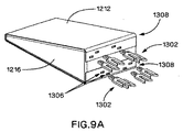
図8Aおよび図8Bは、内部の構成要素を例示するために半透明に図示されたプラグ本体1202を伴う、代替の通信プラグ1200の等角図である。プラグ1200は、複数のワイヤペア1208上を覆って位置する外部絶縁被覆1206を備えるケーブル1204にひずみ緩和ブーツ1214を通して接続されるプラグ本体1202を含む。
8A and 8B are isometric views of an
ワイヤガイド1210はワイヤペア1208のワイヤを位置付け、それによって、そのワイヤは、(図8Aおよび図8Bには図示されていないIDC経由で)本体1210上の回路基板1212と電気的に接触してもよい。本体1210は、好適には、回路基板1212がその上に位置する成型プラスチック本体である。回路基板1212は、好適には、本体1210に取り付けられたフレキシブルプリント回路基板である。他の実装は可能であり得るが、図8A〜図12に例示された例は、成型プラスチック本体に取り付けられたフレキシブルプリント回路基板に関して記載される。
回路基板1212は、TIA‐568‐B.2‐10規格によって要求されるような適切な量のクロストークを提供するために(図12を参照、ワイヤペア1208から接触子1600への)データ経路に結合を導入するように設計される。回路基板1212は、所望のバランスおよびクロストーク性能を実現するように配列された埋め込み型コンデンサおよびインダクタなどの電気的特徴を含んでもよい。電気的特徴の正確な値および配列は、所望の用途やその用途の付随する電気的および/または機械的制約に依存することになる。
The
図9Aおよび図9Bは、図8Aおよび図8Bの代替の通信プラグに使用するためのフレキシブル回路基板1212、本体1216、およびIDC1302を備えるアセンブリの斜視図である。IDC1302は、好適には、本体1216の後端において適切なサイズの孔またはポケット1306に圧入される。ケーブル1204からの各差動ペアは、IDC1302のうちの1つを通して回路基板1212と接触する。
9A and 9B are perspective views of an assembly comprising a
回路基板1212(例示された例においては、フレキシブルプリント回路基板)は、好適には、図9Aおよび図9Bに示されるように、本体1216の後端にわたって曲げられたスズめっきの接触子パッドを含む。孔は、本体1216内の孔またはポケット1306に対応するように回路基板1212に配設されてもよい。次いで、IDC1302が孔またはポケット1306に圧入されると、固有の力が、IDC1302と回路基板1212との間に気密性の接続を生み出し、対応する電気的な接続を生み出す。この形態はまた、回路基板1212を本体1216に固定することにも役に立つ。
The circuit board 1212 (in the illustrated example, a flexible printed circuit board) preferably includes tin-plated contact pads that are bent over the rear end of the
図9A、図9B、および図10Aに示されるように、例示された例では、IDC1302は、本体1216の上部および底部縁1308に向かって、回路基板1212の両端に位置する。このことは、ワイヤペア1208a〜b(図9Aおよび図9Bには図示されない)における個々のワイヤが、IDC1302を通して回路基板1212と接触するときに相対的に分離されることを可能にする。この隣接ワイヤの分離は、差動ペア1208a〜b間のクロストークを低減する。
As shown in FIGS. 9A, 9B, and 10A, in the illustrated example, the
また、図10Aおよび/または図10Bに例示されるものは、プラグ本体1202、ケーブル1204、ワイヤガイド1210、および典型的なRJ45通信ジャックからのジャック接触子アセンブリ1050である。ワイヤガイド1210は、IDC1302との適切かつ繰り返し可能な係合のためにワイヤペア1208a〜bにワイヤを位置付けるために使用される。例えば、ワイヤガイド1210は、IDC1302の位置に対応する場所において個々のワイヤを支えるように構成された複数のスロットおよび/または保持部材を含むことができる。
Also illustrated in FIGS. 10A and / or 10B are a
図11Aおよび図11Bは、図9Aのアセンブリの斜視図であり、2つの代替形態に装着されたIDC1302を示す。図11Aでは、上部IDC1302aおよび下部IDC1302bは、本体1216上の回路基板1212の各端部で整列されたそれぞれの直線列に装着される。図11Bでは、上部IDC1302cは、本体1216の後ろ向きの上部角部に対応する位置において回路基板1212の一端部で装着される。下部IDC1302dは、本体1216の後向きの下部角部に対応する位置において回路基板1212の他の端部で装着される。
11A and 11B are perspective views of the assembly of FIG. 9A showing the
図8Aから図11Bまでに示される設計は、図1Aおよび図1Bに示される典型的なプラグの場合のようにワイヤペア3‐6がワイヤペア4‐5の周りに分割されることを要求しない。分割することは、その代わりに、更に制御された手法で回路基板1212上に実施されることができ、そのことは、プラグに生成されるより小さな「スーパーペア」信号を結果としてもたらすことができる。このことは、ワイヤ終端/IDC1302領域におけるクロストーク複雑性の主な原因を回避する。
The design shown in FIGS. 8A-11B does not require that the wire pair 3-6 be split around the wire pair 4-5 as in the case of the exemplary plug shown in FIGS. 1A and 1B. The splitting can instead be performed on the
図12は、図11Bに示されるアセンブリに類似のアセンブリの下側の斜視図であり、業界標準RJ45ジャックと電気的に接触するための接触子パッド1600を例示する。接触子1600は、好適には、IDC1302とは反対の本体1216の端部で回路基板1212上に位置する8つの金属接触子パッドである。例示された例では、IDC1302は回路基板1212の両端に位置する一方で、接触子パッドは、回路基板1212の長さの中間にまたはその中間あたりに位置する。接触子パッド1600は、好適には、業界標準IEC60603‐7(0.020インチ)に準拠する縁半径を示すように構成される。
FIG. 12 is a bottom perspective view of an assembly similar to the assembly shown in FIG. 11B illustrating a
接触子パッド1600は、回路基板1212が(フレキシブル回路基板の場合には)本体1216の周りに巻き付けられ、その本体1216に取り付けられた後に、回路基板1212上で銅を露出すること、ならびに、銅をニッケルおよび金でめっきすることによって生成されることができる。本体1216の形状は、接触子が準拠した業界標準寸法を有することになることを確実にするために役に立つ。8つの接触子パッド1600は、好適には回路基板1212上のトレースから生成されるので、それらのパッドは本質的に薄く(高さ方向に)、ペア導体間に比較的少ない量の容量性および誘導性の結合をもたらし、その結果として、隣接接触子パッド1600間に非常に少ない結合を導入する。このことは、プラグについてのバランス性能を改善することができる。
The
図13〜図15Bは、上記実施形態に含まれ得る付加的な特徴を例示する。プラグにおける特定のワイヤペア上を伝搬し得る任意のコモンモード信号を減衰することに役立つために、表面実装チョークなどのチョーク(choke)は、回路基板上に含まれてもよい。好適には、1つのチョークがワイヤペアのそれぞれについて含まれる。コモンモードチョークをプラグ設計に組み込むことによって、いくつかのカテゴリ6Aチャネルは、かなり高いレベルの電磁干渉に耐性を有することができる可能性がある。コモンモードチョークは、干渉源によって生じたコモンモード信号を減衰することになり、チャネルにおいてより低い雑音レベルを結果としてもたらす。 13-15B illustrate additional features that may be included in the above embodiments. A choke, such as a surface mount choke, may be included on the circuit board to help attenuate any common mode signal that may propagate on a particular wire pair in the plug. Preferably, one choke is included for each wire pair. By incorporating a common mode choke into the plug design, some Category 6A channels may be able to withstand fairly high levels of electromagnetic interference. The common mode choke will attenuate the common mode signal produced by the interference source, resulting in a lower noise level in the channel.
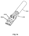
図13および図14は、図2A〜図7の実施形態において実施されるようなチョークの特徴を例示する。図13は、ジャック接触子アセンブリ1050とインターフェースを形成する(プラグ本体202と、ワイヤガイド210と、ケーブル204に接続されたひずみ緩和ブーツ214とを有する)プラグを示す一方で、図14は、ワイヤペア208を有するケーブル204に接続された、プラグの内部の構成要素(例えば、回路基板212)のうちのいくつかを示す。回路基板212は、上部側上に2つのコモンモードチョーク1802aを有するとともに、底部側上に2つのコモンモードチョーク1802bを有する。従って、4つのワイヤペア208のそれぞれの上にコモンモード信号を減衰するための合計4つのチョークがある。
13 and 14 illustrate the features of the choke as implemented in the embodiment of FIGS. FIG. 13 shows a plug (with
図15Aおよび図15Bは、図8A〜図12の実施形態において実施されるようなチョークの特徴を例示し、回路基板1212は、2組のIDC1302a〜b間で成型本体1216の周りに巻き付けられたフレキシブルプリント回路基板である。コモンモードチョーク1802c〜dは、回路基板1212の底部側に取り付けられる。回路基板1212が本体1216の周りに巻き付けられると、チョーク1802c〜dは、本体1216におけるポケット1218内に位置付けられることになる。このことは、本体1216のサイズを大きくすることを可能にする一方で、プラグ全体の寸法を依然として維持する。
FIGS. 15A and 15B illustrate the features of a choke as implemented in the embodiment of FIGS. 8A-12, with the
図16は、図2Aおよび図2Bのプラグに使用されるPCBの2層のレイアウトである。図17は、図2Aおよび図2Bのプラグに使用されるPCBの他の2層のレイアウトである。図17は、図16および図17からの4層全てのPCBレイアウトである。図16〜図18は、追加されたクロストーク要素(C’’’15、C’’’16、C’’’83、およびC’’’84)、ならびにコモンモードチョークの位置のための実施形態を例示する。クロストーク要素は、コンデンサの一方側がPCBの1つの層上にあり、かつコンデンサの他方側がPCBの別の層上にある、パッドコンデンサである。コモンモードチョークは、差動信号用途のために設計されており、それぞれのPCBトレースと直列であるコイルを伴う、コアの周りに巻き付けられた2つの差動コイル/導体のそれぞれを有する単一のフェライトコアを含む。差動信号がチョークを通して伝搬すると、差動導体を通じて同等および反対の電流の流れが存在する。このことは、差動信号のための低インピーダンス経路を結果として生じるフェライトコア内の磁束の取り消しをもたらす。コモンモード信号がチョークを通して伝搬すると、導体を通じる電流の流れは、等しく、伝搬の方向と同じである。このことは、コモンモード信号によって見られるインピーダンスの増加を結果として生じるフェライトコア内の累積的な磁束を生みだす。 FIG. 16 is a two-layer layout of the PCB used for the plugs of FIGS. 2A and 2B. FIG. 17 is another two-layer layout of the PCB used for the plugs of FIGS. 2A and 2B. FIG. 17 is a PCB layout of all four layers from FIGS. 16 and 17. FIGS. 16-18 show implementations for added crosstalk elements (C ′ ″ 15, C ′ ″ 16, C ′ ″ 83, and C ′ ″ 84), and common mode choke positions. The form is illustrated. A crosstalk element is a pad capacitor where one side of the capacitor is on one layer of the PCB and the other side of the capacitor is on another layer of the PCB. A common mode choke is designed for differential signal applications and is a single with each of two differential coils / conductors wrapped around a core with a coil in series with each PCB trace. Includes ferrite core. As the differential signal propagates through the choke, there are equal and opposite current flows through the differential conductor. This results in the cancellation of magnetic flux in the ferrite core resulting in a low impedance path for the differential signal. When a common mode signal propagates through a choke, the current flow through the conductor is equal and the same direction of propagation. This creates a cumulative magnetic flux in the ferrite core that results in the increased impedance seen by the common mode signal.
図1Aおよび図1Bの先行技術のプラグにおいて8つのプラグ接触子および導体の配列を仮定すると、差動ペア間の結合に固有量のアンバランスが存在する。IPC接触領域では、差動ペア1‐2の導体2IPCは、差動ペア1‐2の導体1IPCよりも差動ペア3‐6の導体3IPCの更に近くに近接する(そのことは、図1Aおよび図1Bにおいて明白である)。このことは、差動ペア1‐2の導体1および導体2上の同等でない容量性負荷に起因するモード変換を引き起こすペア1‐2とペア3‐6との間の非対称的なクロストーク関係を結果としてもたらす。ペア1‐2とペア3‐6との間の容量性クロストークは、IPC接触領域におけるこの結合によって支配される。 Assuming an arrangement of eight plug contacts and conductors in the prior art plug of FIGS. 1A and 1B, there is an inherent amount of imbalance in the coupling between the differential pairs. In the IPC contact region, the conductor 2IPC of the differential pair 1-2 is closer to the conductor 3IPC of the differential pair 3-6 than the conductor 1IPC of the differential pair 1-2. This is evident in FIG. 1B). This results in an asymmetric crosstalk relationship between pair 1-2 and pair 3-6 that causes mode conversion due to unequal capacitive loads on conductor 1 and conductor 2 of differential pair 1-2. As a result. Capacitive crosstalk between pair 1-2 and pair 3-6 is dominated by this coupling in the IPC contact area.
図1Aおよび図1Bのプラグ接触子に比較して図6及び図7に示されるようにプラグ接触子の表面積を縮小することによって、接触子間の容量性結合は低減され、それによって、ペア1‐2とペア3‐6との間の固有の非対称的なクロストークは低減される。更には、ペア間の全体的なクロストークもまた、表面積の縮小に起因して低減される。ANSI/TIA‐568‐C.2におけるプラグの差動クロストーク要求に従ったままでいるために、追加的なクロストークが、図16〜図18に示されるように埋め込み型コンデンサの形態でプリント回路基板(PCB)に追加される。ペア1‐2の導体1とペア3‐6の導体6との間に導入されるコンデンサは、PCB上のペア1‐2とペア3‐6との間に非対称的なクロストーク関係を結果としてもたらす。このPCBにおける非対称性は、接触領域の非対称性に関して鏡映される。接触領域内の容量性結合におけるアンバランスにより導入されるモード変換は、PCB上の容量性結合におけるアンバランスにより導入されるモード変換によって相殺される。プラグにおけるペア1‐2とペア3‐6との間の最終的な容量性クロストークは、その時にはバランスが取れており、全てのモード変換は、ペア1‐2の導体1および導体2上の同等の容量性負荷に起因して最小限にされる。 By reducing the surface area of the plug contacts as shown in FIGS. 6 and 7 compared to the plug contacts of FIGS. 1A and 1B, the capacitive coupling between the contacts is reduced, thereby reducing the pair 1 The inherent asymmetric crosstalk between -2 and pair 3-6 is reduced. Furthermore, the overall crosstalk between the pairs is also reduced due to the reduction in surface area. ANSI / TIA-568-C. In order to remain in compliance with the plug's differential crosstalk requirements in FIG. 2, additional crosstalk is added to the printed circuit board (PCB) in the form of embedded capacitors as shown in FIGS. . Capacitors introduced between conductor 1 of pair 1-2 and conductor 6 of pair 3-6 result in an asymmetric crosstalk relationship between pair 1-2 and pair 3-6 on the PCB. Bring. This asymmetry in the PCB is mirrored with respect to the asymmetry of the contact area. The mode conversion introduced by the imbalance in capacitive coupling in the contact area is offset by the mode conversion introduced by the imbalance in capacitive coupling on the PCB. The final capacitive crosstalk between pair 1-2 and pair 3-6 in the plug is then balanced, and all mode conversions are on conductor 1 and conductor 2 of pair 1-2. Minimized due to equivalent capacitive load.
図1Aおよび図1Bの先行技術のプラグにおけるクロストークは、プラグ接触子およびその接触子に接続されたケーブルワイヤの分布型電気的パラメータであって、特に、これらの構成要素の分布インダクタンスおよび容量、ならびにそれらに関連付けられた対応する容量性および誘導性結合を含むパラメータの相関関係にある。しかしながら、結合の支配的なモードは、プラグ接触子に起因して主として容量性であり、そのプラグ接触子は、平板(接触子)の領域に比例するとともにコンデンサ平板(接触子)間の距離に逆比例する静電容量を有する平板コンデンサとしてほぼ考えられることができる。更に、ペア導体間のクロストークは、ペア導体間の静電容量にほぼ比例する。CXYを導体XとYとの間の(接触子間の静電容量に概ね比例する)クロストークと仮定すると、ペア1‐2、3‐6について、ペア1‐2、3‐6の導体間の相対的な距離のために、
ANSI/TIA‐568‐C.2の非埋め込みXTLK範囲内にあるC23−C13+C16−C26(要求1)
および
C23>>C13>>C26>>C16 (関係1)
を得る。C23、C13、C26、およびC16のいずれも等しくないので、関係1(関係1)は非対称的なクロストーク(結合)を示し、ANSI/TIA‐568‐C.2の要求を満たす任意のプラグは、要求1(要求1)に適合しなければならない。また、以下の考察のために、ならびに、接触子2と3との間の結合が、比較的近いことに起因して支配的であるので、
C23−C13+C16−C26=C’23 (式1)
と仮定する。
Crosstalk in the prior art plugs of FIGS. 1A and 1B is a distributed electrical parameter of the plug contact and the cable wire connected to the contact, in particular the distributed inductance and capacitance of these components, And the correlation of parameters including the corresponding capacitive and inductive coupling associated with them. However, the dominant mode of coupling is primarily capacitive due to the plug contact, which is proportional to the area of the flat plate (contact) and the distance between the capacitor flat plates (contacts). It can be almost considered as a flat plate capacitor having an inversely proportional capacitance. Furthermore, the crosstalk between the pair conductors is substantially proportional to the capacitance between the pair conductors. Assuming CXY is crosstalk between conductors X and Y (generally proportional to the capacitance between the contacts), for pairs 1-2 and 3-6, between the conductors of pairs 1-2 and 3-6 Because of the relative distance of
ANSI / TIA-568-C. C23-C13 + C16-C26 within 2 non-embedded XTLK range (request 1)
And C23 >> C13 >> C26 >> C16 (Relation 1)
Get. Since none of C23, C13, C26, and C16 are equal, relation 1 (relation 1) exhibits asymmetric crosstalk and ANSI / TIA-568-C. Any plug that meets requirement 2 must meet requirement 1 (requirement 1). Also for the following considerations, and because the coupling between the contacts 2 and 3 is dominant due to the relatively closeness,
C23−C13 + C16−C26 = C′23 (Formula 1)
Assume that
対称的に、本発明は、接触領域の縮小に起因してプラグ接触領域におけるクロストークが低減され、また、PCBに接続される分離した、新規のIDC要素にプラグ接触子の絶縁貫通の特徴を分離することに起因してクロストークが低減されており、IDC要素は、前記したように、部分的にバランスの取れたまたはバランスの取れた方向に編成されることができる。本発明において、新規のプラグ接触子のクロストーク結合C”23、C”13、C”16、C”26のそれぞれは、先行技術のプラグにおけるそれらの相対物C23、C13、C16、C26のそれぞれよりも個々に小さい。その結果として、C”23、C”13、C”16、C”26は式1(式1)に代入され、その式の左辺は、そのC’23よりも小さく、要求1はまた満たされず、すなわち、C”23−C”13+C”16−C”26は、ANSI/TIA‐568‐C.2の非埋め込みXTLK範囲の外側にあることができる。C”23、C”13、C”16、C”26は、それらが全て等しくないので、依然として非対称的なクロストーク(結合)を含む。新規のプラグ接触子のクロストークC”23、C”13、C”16、C”26の低減は、本発明において有利に使用される少なくとも1つの設計自由度を与える。 In contrast, the present invention reduces the crosstalk in the plug contact area due to the reduction of the contact area and also provides the isolated through-hole feature of the plug contact to a separate, new IDC element connected to the PCB. Crosstalk is reduced due to the separation and the IDC elements can be knitted in a partially balanced or balanced direction as described above. In the present invention, each of the novel plug contact crosstalk couplings C ″ 23, C ″ 13, C ″ 16, C ″ 26 is represented by their respective counterparts C23, C13, C16, C26 in the prior art plug. Smaller than individual. As a result, C ″ 23, C ″ 13, C ″ 16, and C ″ 26 are assigned to Equation 1 (Equation 1), and the left side of the equation is smaller than C′23, and requirement 1 is not satisfied again. That is, C "23-C" 13 + C "16-C" 26 is ANSI / TIA-568-C. It can be outside the 2 non-embedded XTLK range. C ″ 23, C ″ 13, C ″ 16, C ″ 26 still contain asymmetric crosstalk because they are not all equal. The reduction of the novel plug contact crosstalk C "23, C" 13, C "16, C" 26 provides at least one degree of design freedom that is advantageously used in the present invention.
本発明は、C”23−C”13+C”16−C”26+C’’’16がANSI/TIA‐568‐C.2の非埋め込みXTLK範囲内にあるように、非対称的なクロストークにおいてPCB内に要素C’’’16を追加する。更に、C’’’16の値は、
C”23−C”13+C”16−C”26=C’’’23(効果的なプラグ接触子クロストーク)=C’’’16(式2)
であるように選択される。接触導体(2‐3)に比較して新規の効果的なプラグ接触子クロストークC’’’23が間で効果的である場合、C’’’16が反対の接触導体(1‐6)間に配設されるので、C’’’16は、鏡映されたクロストーク要素である。C’’’16は、このペアの組み合わせについての他の固有のプラグPCB結合要素という点で第2の非対称的な結合要素であり、そのPCB結合要素は、PCB伝送線路の分布型電気的パラメータに起因し、C’’’16よりも非常に低い値を有する。C’’’16が固有の非対称的な結合C’’’23と組み合わされると、式2の同等性、またはほぼ同等性のために、バランスの取れた対称的な結合が、このペアの組み合わせの個別の接触子間に存在する。本発明には、ペア1‐2の各導体上の同等の容量性負荷に起因するモード変換を最小限にすることをもたらすこのペアの組み合わせについて個別の接触子間にバランスの取れた対称的な結合が存在する。
In the present invention, C "23-C" 13 + C "16-C" 26 + C '"16 is ANSI / TIA-568-C. Add an element C ′ ″ 16 in the PCB at asymmetric crosstalk so that it is in the 2 non-embedded XTLK range. Furthermore, the value of C ′ ″ 16 is
C ″ 23−C ″ 13 + C ″ 16−C ″ 26 = C ′ ″ 23 (effective plug contact crosstalk) = C ′ ″ 16 (formula 2)
Selected to be. When the new effective plug contact crosstalk C ′ ″ 23 is effective between the contact conductor (2-3), C ′ ″ 16 is the opposite contact conductor (1-6). C ′ ″ 16 is a mirrored crosstalk element as it is disposed between. C ″ ′16 is the second asymmetric coupling element in terms of other unique plug PCB coupling elements for this pair combination, which is the distributed electrical parameter of the PCB transmission line. Due to the above, it has a value much lower than C ′ ″ 16. When C ″ ′16 is combined with an inherently asymmetric coupling C ′ ″ 23, a balanced symmetric coupling is a combination of this pair because of the equality or near equality of Equation 2. Between the individual contacts. The present invention provides a balanced symmetrical between the individual contacts for this pair combination that results in minimizing mode conversion due to equivalent capacitive loads on each conductor of pair 1-2. There is a bond.
同じ技術は、ペア1‐2およびペア4‐5(構成要素C’’’15を参照)、ペア3‐6およびペア7‐8(構成要素C’’’83を参照)、ならびにペア4‐5およびペア7‐8(構成要素C’’’84を参照)に関してPCB上で適用される。ペアの組み合わせ3‐6、4‐5の場合、その組み合せは、ペア4‐5の周りの分割ペア3‐6のために自然にバランスの取れた対称的な結合であるが、このペアの組み合わせについてのクロストークのレベルが非埋め込み範囲内に上げられる必要がある場合、結合は、ほぼ同等の量で3‐4と5‐6との間に追加されることができる。これらのペア間の分離および対応する低レベルのクロストークのために、ペアの組み合わせ1‐2、7‐8は重要ではない。IDCのバランスの取れた特徴は、前記したようなIDCレイアウトもプラグの固有の非対称的な結合を低減するという点において、本発明に有利に使用される少なくとも1つの設計自由度を与える。 The same technique is used for pair 1-2 and pair 4-5 (see component C ′ ″ 15), pair 3-6 and pair 7-8 (see component C ′ ″ 83), and pair 4- 5 and pair 7-8 (see component C ′ ″ 84) apply on PCB. In the case of pair combination 3-6, 4-5, the combination is a naturally balanced symmetrical combination for split pair 3-6 around pair 4-5, but this pair combination If the level of crosstalk for needs to be raised within the non-embedded range, coupling can be added between 3-4 and 5-6 in approximately equivalent amounts. Because of the separation between these pairs and the corresponding low level of crosstalk, the pair combinations 1-2, 7-8 are not important. The balanced features of the IDC provide at least one design degree of freedom that is advantageously used in the present invention in that the IDC layout as described above also reduces the inherent asymmetric coupling of the plug.
本発明は好適な設計を有するように記載されたが、本発明は、この開示の趣旨および範囲内で更に改変されることができる。従って、本出願は、本発明の一般原理を用いて本発明のいかなる変形、使用、または改造を包含することが意図される。更に、この出願は、本発明が属するおよび添付の特許請求の範囲内にある当技術分野における周知または通例の慣行の範疇にあるような本開示からの逸脱を包含することが意図される。 While this invention has been described as having a preferred design, the present invention can be further modified within the spirit and scope of this disclosure. This application is therefore intended to cover any variations, uses, or adaptations of the invention using its general principles. Furthermore, this application is intended to cover departures from this disclosure as falling within the scope of well-known or customary practice in the art to which this invention belongs and that is within the scope of the appended claims.
108 208 (ワイヤ)ペア
200 通信プラグ
202 プラグ本体
204 ケーブル
206 外部絶縁被覆
210 ワイヤガイド
212 回路基板
214 緩和ブーツ。
300 アセンブリ
304 接触子
108 208 (wire)
300
Claims (14)
軸に沿ってプラグ本体に入る前記通信ケーブルを収容するための空洞を有する当該プラグ本体と、
前記空洞内に位置し、複数のトレースを有し、前記軸に対して角度が付いた少なくとも1つの表面を有する回路基板と、
前記回路基板上のトレースと前記通信ケーブルとを電気的に接触させるための第1の接触子であって、特定のワイヤペアの接触子が複数の別のワイヤペアの接触子の両方と等距離になるように前記第1の接触子は千鳥状に配置される、第1の接触子と、
前記回路基板上の前記トレースと前記プラグがインターフェースを形成するジャック上の接触子とを電気的に接触させるための第2の接触子と、
を備える、通信プラグ。 A communication plug for making electrical contact between a communication cable and a communication jack,
The plug body having a cavity for receiving the communication cable entering the plug body along an axis;
A circuit board located in the cavity, having a plurality of traces and having at least one surface angled with respect to the axis;
A first contact for electrically contacting the trace on the circuit board and the communication cable, wherein a contact of a specific wire pair is equidistant from both of the contacts of a plurality of other wire pairs The first contacts are arranged in a staggered manner, and the first contacts,
A second contact for making electrical contact between the trace on the circuit board and the contact on the jack to which the plug forms an interface;
A communication plug.
Applications Claiming Priority (3)
| Application Number | Priority Date | Filing Date | Title |
|---|---|---|---|
| US12/909,130 | 2010-10-21 | ||
| US12/909,130 US20110093890A1 (en) | 2009-10-21 | 2010-10-21 | User control interface for interactive digital television |
| PCT/US2011/052862 WO2012054173A1 (en) | 2010-10-21 | 2011-09-23 | Communication plug with improved crosstalk |
Publications (3)
| Publication Number | Publication Date |
|---|---|
| JP2013544010A JP2013544010A (en) | 2013-12-09 |
| JP2013544010A5 JP2013544010A5 (en) | 2014-10-23 |
| JP5654132B2 true JP5654132B2 (en) | 2015-01-14 |
Family
ID=44759788
Family Applications (1)
| Application Number | Title | Priority Date | Filing Date |
|---|---|---|---|
| JP2013534919A Active JP5654132B2 (en) | 2010-10-21 | 2011-09-23 | Communication plug with improved crosstalk |
Country Status (2)
| Country | Link |
|---|---|
| JP (1) | JP5654132B2 (en) |
| WO (1) | WO2012054173A1 (en) |
Families Citing this family (5)
| Publication number | Priority date | Publication date | Assignee | Title |
|---|---|---|---|---|
| US9300092B1 (en) * | 2014-09-30 | 2016-03-29 | Optical Cable Corporation | High frequency RJ45 plug with non-continuous ground planes for cross talk control |
| MX2018006739A (en) | 2015-12-15 | 2018-08-01 | Panduit Corp | Field terminable rj45 plug assembly. |
| BE1026802B1 (en) * | 2018-11-26 | 2020-06-25 | Phoenix Contact Gmbh & Co | Connectors |
| DE102020129353A1 (en) * | 2020-11-06 | 2022-05-12 | Weidmüller Interface GmbH & Co. KG | Housing with a connection system for implementing branches on a plurality of continuous electrical conductors |
| DE102022127543A1 (en) | 2022-10-19 | 2024-04-25 | Weidmüller Interface GmbH & Co. KG | Plug-in arrangement and Ethernet data connector |
Family Cites Families (4)
| Publication number | Priority date | Publication date | Assignee | Title |
|---|---|---|---|---|
| US5999400A (en) * | 1998-11-30 | 1999-12-07 | Berg Technology, Inc. | Modular plug with electronic components |
| US7341493B2 (en) * | 2006-05-17 | 2008-03-11 | Tyco Electronics Corporation | Electrical connector having staggered contacts |
| CN101595536B (en) * | 2006-12-01 | 2013-03-06 | 西蒙公司 | Modular connector with reduced termination variability |
| DE102008027512B4 (en) * | 2008-06-10 | 2010-07-01 | Tyco Electronics Amp Gmbh | Electric plug |
-
2011
- 2011-09-23 JP JP2013534919A patent/JP5654132B2/en active Active
- 2011-09-23 WO PCT/US2011/052862 patent/WO2012054173A1/en active Application Filing
Also Published As
| Publication number | Publication date |
|---|---|
| WO2012054173A1 (en) | 2012-04-26 |
| JP2013544010A (en) | 2013-12-09 |
Similar Documents
| Publication | Publication Date | Title |
|---|---|---|
| US11600960B2 (en) | Communications plug with improved crosstalk | |
| US8915756B2 (en) | Communication connector having a printed circuit board with thin conductive layers | |
| US7201618B2 (en) | Controlled mode conversion connector for reduced alien crosstalk | |
| US7967645B2 (en) | High speed data communications connector circuits, systems, and methods for reducing crosstalk in communications systems | |
| US10530098B2 (en) | Connector with capacitive crosstalk compensation to reduce alien crosstalk | |
| US8353723B2 (en) | Communications patching devices having capacitor-based multi-stage near-end alien crosstalk compensation circuits between adjacent connector ports | |
| JP2013510404A (en) | Communication connector with improved crosstalk compensation | |
| US9246274B2 (en) | Communication connectors having crosstalk compensation networks | |
| JP5654132B2 (en) | Communication plug with improved crosstalk | |
| EP3175515B1 (en) | Communications connectors including low impedance transmission line segments that improve return loss | |
| US10559927B2 (en) | Switchable RJ45/ARJ45 jack | |
| TW201414116A (en) | Pin structure of RJ connector, RJ connector module and RJ connector system using the same | |
| US10734765B2 (en) | Connector with capacitive crosstalk compensation |
Legal Events
| Date | Code | Title | Description |
|---|---|---|---|
| A521 | Request for written amendment filed |
Free format text: JAPANESE INTERMEDIATE CODE: A523 Effective date: 20140905 |
|
| A621 | Written request for application examination |
Free format text: JAPANESE INTERMEDIATE CODE: A621 Effective date: 20140905 |
|
| A871 | Explanation of circumstances concerning accelerated examination |
Free format text: JAPANESE INTERMEDIATE CODE: A871 Effective date: 20140905 |
|
| A975 | Report on accelerated examination |
Free format text: JAPANESE INTERMEDIATE CODE: A971005 Effective date: 20140926 |
|
| TRDD | Decision of grant or rejection written | ||
| A01 | Written decision to grant a patent or to grant a registration (utility model) |
Free format text: JAPANESE INTERMEDIATE CODE: A01 Effective date: 20141020 |
|
| A61 | First payment of annual fees (during grant procedure) |
Free format text: JAPANESE INTERMEDIATE CODE: A61 Effective date: 20141119 |
|
| R150 | Certificate of patent or registration of utility model |
Ref document number: 5654132 Country of ref document: JP Free format text: JAPANESE INTERMEDIATE CODE: R150 |
|
| R250 | Receipt of annual fees |
Free format text: JAPANESE INTERMEDIATE CODE: R250 |
|
| R250 | Receipt of annual fees |
Free format text: JAPANESE INTERMEDIATE CODE: R250 |
|
| R250 | Receipt of annual fees |
Free format text: JAPANESE INTERMEDIATE CODE: R250 |
|
| R250 | Receipt of annual fees |
Free format text: JAPANESE INTERMEDIATE CODE: R250 |
|
| R250 | Receipt of annual fees |
Free format text: JAPANESE INTERMEDIATE CODE: R250 |
|
| R250 | Receipt of annual fees |
Free format text: JAPANESE INTERMEDIATE CODE: R250 |
|
| R250 | Receipt of annual fees |
Free format text: JAPANESE INTERMEDIATE CODE: R250 |