JP5653880B2 - Resist underlayer film forming material and pattern forming method - Google Patents
Resist underlayer film forming material and pattern forming method Download PDFInfo
- Publication number
- JP5653880B2 JP5653880B2 JP2011224290A JP2011224290A JP5653880B2 JP 5653880 B2 JP5653880 B2 JP 5653880B2 JP 2011224290 A JP2011224290 A JP 2011224290A JP 2011224290 A JP2011224290 A JP 2011224290A JP 5653880 B2 JP5653880 B2 JP 5653880B2
- Authority
- JP
- Japan
- Prior art keywords
- film
- resist
- pattern
- resist underlayer
- underlayer film
- Prior art date
- Legal status (The legal status is an assumption and is not a legal conclusion. Google has not performed a legal analysis and makes no representation as to the accuracy of the status listed.)
- Active
Links
Images


Classifications
-
- G—PHYSICS
- G03—PHOTOGRAPHY; CINEMATOGRAPHY; ANALOGOUS TECHNIQUES USING WAVES OTHER THAN OPTICAL WAVES; ELECTROGRAPHY; HOLOGRAPHY
- G03F—PHOTOMECHANICAL PRODUCTION OF TEXTURED OR PATTERNED SURFACES, e.g. FOR PRINTING, FOR PROCESSING OF SEMICONDUCTOR DEVICES; MATERIALS THEREFOR; ORIGINALS THEREFOR; APPARATUS SPECIALLY ADAPTED THEREFOR
- G03F7/00—Photomechanical, e.g. photolithographic, production of textured or patterned surfaces, e.g. printing surfaces; Materials therefor, e.g. comprising photoresists; Apparatus specially adapted therefor
- G03F7/004—Photosensitive materials
- G03F7/09—Photosensitive materials characterised by structural details, e.g. supports, auxiliary layers
- G03F7/091—Photosensitive materials characterised by structural details, e.g. supports, auxiliary layers characterised by antireflection means or light filtering or absorbing means, e.g. anti-halation, contrast enhancement
-
- G—PHYSICS
- G03—PHOTOGRAPHY; CINEMATOGRAPHY; ANALOGOUS TECHNIQUES USING WAVES OTHER THAN OPTICAL WAVES; ELECTROGRAPHY; HOLOGRAPHY
- G03F—PHOTOMECHANICAL PRODUCTION OF TEXTURED OR PATTERNED SURFACES, e.g. FOR PRINTING, FOR PROCESSING OF SEMICONDUCTOR DEVICES; MATERIALS THEREFOR; ORIGINALS THEREFOR; APPARATUS SPECIALLY ADAPTED THEREFOR
- G03F7/00—Photomechanical, e.g. photolithographic, production of textured or patterned surfaces, e.g. printing surfaces; Materials therefor, e.g. comprising photoresists; Apparatus specially adapted therefor
- G03F7/004—Photosensitive materials
- G03F7/09—Photosensitive materials characterised by structural details, e.g. supports, auxiliary layers
- G03F7/094—Multilayer resist systems, e.g. planarising layers
-
- G—PHYSICS
- G03—PHOTOGRAPHY; CINEMATOGRAPHY; ANALOGOUS TECHNIQUES USING WAVES OTHER THAN OPTICAL WAVES; ELECTROGRAPHY; HOLOGRAPHY
- G03F—PHOTOMECHANICAL PRODUCTION OF TEXTURED OR PATTERNED SURFACES, e.g. FOR PRINTING, FOR PROCESSING OF SEMICONDUCTOR DEVICES; MATERIALS THEREFOR; ORIGINALS THEREFOR; APPARATUS SPECIALLY ADAPTED THEREFOR
- G03F7/00—Photomechanical, e.g. photolithographic, production of textured or patterned surfaces, e.g. printing surfaces; Materials therefor, e.g. comprising photoresists; Apparatus specially adapted therefor
- G03F7/004—Photosensitive materials
- G03F7/09—Photosensitive materials characterised by structural details, e.g. supports, auxiliary layers
- G03F7/095—Photosensitive materials characterised by structural details, e.g. supports, auxiliary layers having more than one photosensitive layer
-
- G—PHYSICS
- G03—PHOTOGRAPHY; CINEMATOGRAPHY; ANALOGOUS TECHNIQUES USING WAVES OTHER THAN OPTICAL WAVES; ELECTROGRAPHY; HOLOGRAPHY
- G03F—PHOTOMECHANICAL PRODUCTION OF TEXTURED OR PATTERNED SURFACES, e.g. FOR PRINTING, FOR PROCESSING OF SEMICONDUCTOR DEVICES; MATERIALS THEREFOR; ORIGINALS THEREFOR; APPARATUS SPECIALLY ADAPTED THEREFOR
- G03F7/00—Photomechanical, e.g. photolithographic, production of textured or patterned surfaces, e.g. printing surfaces; Materials therefor, e.g. comprising photoresists; Apparatus specially adapted therefor
- G03F7/004—Photosensitive materials
- G03F7/09—Photosensitive materials characterised by structural details, e.g. supports, auxiliary layers
- G03F7/11—Photosensitive materials characterised by structural details, e.g. supports, auxiliary layers having cover layers or intermediate layers, e.g. subbing layers
-
- G—PHYSICS
- G03—PHOTOGRAPHY; CINEMATOGRAPHY; ANALOGOUS TECHNIQUES USING WAVES OTHER THAN OPTICAL WAVES; ELECTROGRAPHY; HOLOGRAPHY
- G03F—PHOTOMECHANICAL PRODUCTION OF TEXTURED OR PATTERNED SURFACES, e.g. FOR PRINTING, FOR PROCESSING OF SEMICONDUCTOR DEVICES; MATERIALS THEREFOR; ORIGINALS THEREFOR; APPARATUS SPECIALLY ADAPTED THEREFOR
- G03F7/00—Photomechanical, e.g. photolithographic, production of textured or patterned surfaces, e.g. printing surfaces; Materials therefor, e.g. comprising photoresists; Apparatus specially adapted therefor
- G03F7/20—Exposure; Apparatus therefor
- G03F7/2041—Exposure; Apparatus therefor in the presence of a fluid, e.g. immersion; using fluid cooling means
-
- G—PHYSICS
- G03—PHOTOGRAPHY; CINEMATOGRAPHY; ANALOGOUS TECHNIQUES USING WAVES OTHER THAN OPTICAL WAVES; ELECTROGRAPHY; HOLOGRAPHY
- G03F—PHOTOMECHANICAL PRODUCTION OF TEXTURED OR PATTERNED SURFACES, e.g. FOR PRINTING, FOR PROCESSING OF SEMICONDUCTOR DEVICES; MATERIALS THEREFOR; ORIGINALS THEREFOR; APPARATUS SPECIALLY ADAPTED THEREFOR
- G03F7/00—Photomechanical, e.g. photolithographic, production of textured or patterned surfaces, e.g. printing surfaces; Materials therefor, e.g. comprising photoresists; Apparatus specially adapted therefor
- G03F7/26—Processing photosensitive materials; Apparatus therefor
- G03F7/30—Imagewise removal using liquid means
-
- G—PHYSICS
- G03—PHOTOGRAPHY; CINEMATOGRAPHY; ANALOGOUS TECHNIQUES USING WAVES OTHER THAN OPTICAL WAVES; ELECTROGRAPHY; HOLOGRAPHY
- G03F—PHOTOMECHANICAL PRODUCTION OF TEXTURED OR PATTERNED SURFACES, e.g. FOR PRINTING, FOR PROCESSING OF SEMICONDUCTOR DEVICES; MATERIALS THEREFOR; ORIGINALS THEREFOR; APPARATUS SPECIALLY ADAPTED THEREFOR
- G03F7/00—Photomechanical, e.g. photolithographic, production of textured or patterned surfaces, e.g. printing surfaces; Materials therefor, e.g. comprising photoresists; Apparatus specially adapted therefor
- G03F7/26—Processing photosensitive materials; Apparatus therefor
- G03F7/36—Imagewise removal not covered by groups G03F7/30 - G03F7/34, e.g. using gas streams, using plasma
-
- H—ELECTRICITY
- H01—ELECTRIC ELEMENTS
- H01L—SEMICONDUCTOR DEVICES NOT COVERED BY CLASS H10
- H01L21/00—Processes or apparatus adapted for the manufacture or treatment of semiconductor or solid state devices or of parts thereof
- H01L21/02—Manufacture or treatment of semiconductor devices or of parts thereof
- H01L21/027—Making masks on semiconductor bodies for further photolithographic processing not provided for in group H01L21/18 or H01L21/34
- H01L21/0271—Making masks on semiconductor bodies for further photolithographic processing not provided for in group H01L21/18 or H01L21/34 comprising organic layers
-
- H—ELECTRICITY
- H01—ELECTRIC ELEMENTS
- H01L—SEMICONDUCTOR DEVICES NOT COVERED BY CLASS H10
- H01L21/00—Processes or apparatus adapted for the manufacture or treatment of semiconductor or solid state devices or of parts thereof
- H01L21/02—Manufacture or treatment of semiconductor devices or of parts thereof
- H01L21/04—Manufacture or treatment of semiconductor devices or of parts thereof the devices having at least one potential-jump barrier or surface barrier, e.g. PN junction, depletion layer or carrier concentration layer
- H01L21/18—Manufacture or treatment of semiconductor devices or of parts thereof the devices having at least one potential-jump barrier or surface barrier, e.g. PN junction, depletion layer or carrier concentration layer the devices having semiconductor bodies comprising elements of Group IV of the Periodic System or AIIIBV compounds with or without impurities, e.g. doping materials
- H01L21/30—Treatment of semiconductor bodies using processes or apparatus not provided for in groups H01L21/20 - H01L21/26
- H01L21/31—Treatment of semiconductor bodies using processes or apparatus not provided for in groups H01L21/20 - H01L21/26 to form insulating layers thereon, e.g. for masking or by using photolithographic techniques; After treatment of these layers; Selection of materials for these layers
- H01L21/3105—After-treatment
- H01L21/311—Etching the insulating layers by chemical or physical means
- H01L21/31105—Etching inorganic layers
- H01L21/31111—Etching inorganic layers by chemical means
- H01L21/31116—Etching inorganic layers by chemical means by dry-etching
-
- H—ELECTRICITY
- H01—ELECTRIC ELEMENTS
- H01L—SEMICONDUCTOR DEVICES NOT COVERED BY CLASS H10
- H01L21/00—Processes or apparatus adapted for the manufacture or treatment of semiconductor or solid state devices or of parts thereof
- H01L21/02—Manufacture or treatment of semiconductor devices or of parts thereof
- H01L21/04—Manufacture or treatment of semiconductor devices or of parts thereof the devices having at least one potential-jump barrier or surface barrier, e.g. PN junction, depletion layer or carrier concentration layer
- H01L21/18—Manufacture or treatment of semiconductor devices or of parts thereof the devices having at least one potential-jump barrier or surface barrier, e.g. PN junction, depletion layer or carrier concentration layer the devices having semiconductor bodies comprising elements of Group IV of the Periodic System or AIIIBV compounds with or without impurities, e.g. doping materials
- H01L21/30—Treatment of semiconductor bodies using processes or apparatus not provided for in groups H01L21/20 - H01L21/26
- H01L21/31—Treatment of semiconductor bodies using processes or apparatus not provided for in groups H01L21/20 - H01L21/26 to form insulating layers thereon, e.g. for masking or by using photolithographic techniques; After treatment of these layers; Selection of materials for these layers
- H01L21/3105—After-treatment
- H01L21/311—Etching the insulating layers by chemical or physical means
- H01L21/31127—Etching organic layers
- H01L21/31133—Etching organic layers by chemical means
- H01L21/31138—Etching organic layers by chemical means by dry-etching
-
- H—ELECTRICITY
- H01—ELECTRIC ELEMENTS
- H01L—SEMICONDUCTOR DEVICES NOT COVERED BY CLASS H10
- H01L21/00—Processes or apparatus adapted for the manufacture or treatment of semiconductor or solid state devices or of parts thereof
- H01L21/02—Manufacture or treatment of semiconductor devices or of parts thereof
- H01L21/04—Manufacture or treatment of semiconductor devices or of parts thereof the devices having at least one potential-jump barrier or surface barrier, e.g. PN junction, depletion layer or carrier concentration layer
- H01L21/18—Manufacture or treatment of semiconductor devices or of parts thereof the devices having at least one potential-jump barrier or surface barrier, e.g. PN junction, depletion layer or carrier concentration layer the devices having semiconductor bodies comprising elements of Group IV of the Periodic System or AIIIBV compounds with or without impurities, e.g. doping materials
- H01L21/30—Treatment of semiconductor bodies using processes or apparatus not provided for in groups H01L21/20 - H01L21/26
- H01L21/31—Treatment of semiconductor bodies using processes or apparatus not provided for in groups H01L21/20 - H01L21/26 to form insulating layers thereon, e.g. for masking or by using photolithographic techniques; After treatment of these layers; Selection of materials for these layers
- H01L21/3105—After-treatment
- H01L21/311—Etching the insulating layers by chemical or physical means
- H01L21/31144—Etching the insulating layers by chemical or physical means using masks
-
- C—CHEMISTRY; METALLURGY
- C08—ORGANIC MACROMOLECULAR COMPOUNDS; THEIR PREPARATION OR CHEMICAL WORKING-UP; COMPOSITIONS BASED THEREON
- C08J—WORKING-UP; GENERAL PROCESSES OF COMPOUNDING; AFTER-TREATMENT NOT COVERED BY SUBCLASSES C08B, C08C, C08F, C08G or C08H
- C08J3/00—Processes of treating or compounding macromolecular substances
- C08J3/24—Crosslinking, e.g. vulcanising, of macromolecules
Description
本発明は、レジスト下層膜形成材料及びこれを用いたパターン形成方法に関する。 The present invention relates to a resist underlayer film forming material and a pattern forming method using the same.
近年、LSIの高集積化と高速度化に伴い、パターンルールの微細化が求められている中、現在汎用技術として用いられている光露光を用いたリソグラフィーにおいては、光源の波長に由来する本質的な解像度の限界に近づきつつある。 In recent years, with the increasing integration and speed of LSIs, there is a need for finer pattern rules. In lithography using light exposure, which is currently used as a general-purpose technology, the essence derived from the wavelength of the light source The resolution limit is approaching.
レジストパターン形成の際に使用するリソグラフィー用の光源として、水銀灯のg線(436nm)もしくはi線(365nm)を光源とする光露光が用いられ、更なる微細化のための手段として、露光光を短波長化する方法が有効とされ、露光光源としてi線(365nm)に代わって短波長のKrFエキシマレーザー(248nm)、特にArFエキシマレーザー(193nm)、更にはNAが1.35のArFエキシマレーザーを用いた液浸リソグラフィーを用いたリソグラフィーが用いられ、これで得られたパターンピッチを倍化するダブルパターニングでの量産が開始されている。 Light exposure using mercury lamp g-line (436 nm) or i-line (365 nm) as a light source for lithography used for resist pattern formation is used, and exposure light is used as a means for further miniaturization. A method of shortening the wavelength is effective, and instead of i-line (365 nm) as an exposure light source, a short wavelength KrF excimer laser (248 nm), particularly an ArF excimer laser (193 nm), and an ArF excimer laser with NA of 1.35 Lithography using immersion lithography using a photolithography is used, and mass production by double patterning that doubles the pattern pitch obtained by this has been started.
一方、従来、段差基板上に高アスペクト比のパターンを形成するには2層プロセスが優れていることが知られており、更に、2層レジスト膜を一般的なアルカリ現像液で現像するためには、ヒドロキシ基やカルボキシル基等の親水基を有する高分子シリコーン化合物が必要である。 On the other hand, conventionally, it is known that a two-layer process is excellent for forming a pattern with a high aspect ratio on a stepped substrate, and further, for developing a two-layer resist film with a general alkali developer. Requires a high molecular silicone compound having a hydrophilic group such as a hydroxy group or a carboxyl group.
シリコーン系化学増幅ポジ型レジスト材料としては、安定なアルカリ可溶性シリコーンポリマーであるポリヒドロキシベンジルシルセスキオキサンのフェノール性水酸基の一部をt−Boc基で保護したものをベース樹脂として使用し、これと酸発生剤とを組み合わせたKrFエキシマレーザー用シリコーン系化学増幅ポジ型レジスト材料が提案された。また、ArFエキシマレーザー用としては、シクロヘキシルカルボン酸を酸不安定基で置換したタイプのシルセスキオキサンをベースにしたポジ型レジスト材料が提案されている。更に、F2レーザー用としては、ヘキサフルオロイソプロパノールを溶解性基として持つシルセスキオキサンをベースにしたポジ型レジスト材料が提案されている。上記ポリマーは、トリアルコキシシラン、又はトリハロゲン化シランの縮重合によるラダー骨格を含むポリシルセスキオキサンを主鎖に含むものである。 As the silicone-based chemically amplified positive resist material, a base resin in which a part of the phenolic hydroxyl group of polyhydroxybenzylsilsesquioxane, which is a stable alkali-soluble silicone polymer, is protected with a t-Boc group is used. A silicone-based chemically amplified positive resist material for KrF excimer lasers, which is a combination of an acid generator and an acid generator, has been proposed. For ArF excimer lasers, a positive resist material based on silsesquioxane in which cyclohexyl carboxylic acid is substituted with an acid labile group has been proposed. Furthermore, for F 2 lasers, positive resist materials based on silsesquioxane having hexafluoroisopropanol as a soluble group have been proposed. The above polymer contains polysilsesquioxane having a ladder skeleton formed by condensation polymerization of trialkoxysilane or trihalogenated silane in the main chain.
珪素が側鎖にペンダントされたレジスト用ベースポリマーとしては、珪素含有(メタ)アクリルエステル系ポリマーが提案されている。 A silicon-containing (meth) acrylic ester polymer has been proposed as a resist base polymer in which silicon is pendant to the side chain.
2層プロセスのレジスト下層膜としては、酸素ガスによるエッチングが可能な炭化水素化合物であり、更にその下の基板をエッチングする場合におけるマスクになるため、高いエッチング耐性を有することが必要である。酸素ガスエッチングにおいては、珪素原子を含まない炭化水素のみで構成される必要がある。また、上層の珪素含有レジスト膜の線幅制御性を向上させ、定在波によるパターン側壁の凹凸とパターンの崩壊を低減させるためには、反射防止膜としての機能も有し、具体的にはレジスト下層膜からレジスト上層膜内への反射率を1%以下に抑える必要がある。 The resist underlayer film of the two-layer process is a hydrocarbon compound that can be etched with oxygen gas, and further needs to have high etching resistance because it serves as a mask for etching the underlying substrate. In oxygen gas etching, it is necessary to be composed only of hydrocarbons that do not contain silicon atoms. In addition, in order to improve the line width controllability of the upper silicon-containing resist film and reduce the pattern sidewall irregularities and pattern collapse due to standing waves, it also has a function as an antireflection film, specifically It is necessary to suppress the reflectance from the resist lower layer film into the resist upper layer film to 1% or less.
ここで、最大500nmの膜厚までの反射率を計算した結果を図3,4に示す。露光波長は193nm、レジスト上層膜の屈折率n値を1.74、屈折率k値を0.02と仮定し、図3ではレジスト下層膜のk値を0.3に固定し、縦軸にn値を1.0〜2.0、横軸に膜厚0〜500nmの範囲で変動させたときの基板反射率を示す。膜厚が300nm以上の2層プロセス用レジスト下層膜を想定した場合、レジスト上層膜と同程度かあるいはそれよりも少し屈折率が高いn値が1.6〜1.9の範囲で反射率を1%以下にできる最適値が存在する。 Here, the results of calculating the reflectance up to a maximum film thickness of 500 nm are shown in FIGS. Assuming that the exposure wavelength is 193 nm, the refractive index n value of the resist upper layer film is 1.74, and the refractive index k value is 0.02, the k value of the resist lower layer film is fixed at 0.3 in FIG. The substrate reflectivity when the n value is varied in the range of 1.0 to 2.0 and the film thickness in the range of 0 to 500 nm is shown on the horizontal axis. Assuming a resist underlayer film for a two-layer process having a film thickness of 300 nm or more, the reflectivity is in the range of n to 1.6 to 1.9, which has a refractive index that is the same as or slightly higher than the resist upper layer film. There is an optimum value that can be reduced to 1% or less.
また、図4では、レジスト下層膜のn値を1.5に固定し、k値を0〜0.8の範囲で変動させたときの反射率を示す。膜厚が300nm以上の2層プロセス用レジスト下層膜を想定した場合、k値が0.24〜0.15の範囲で反射率を1%以下にすることが可能である。一方、40nm程度の薄膜で用いられる単層レジスト用の反射防止膜の最適k値は0.4〜0.5であり、300nm以上で用いられる2層プロセス用のレジスト下層膜の最適k値とは異なる。2層プロセス用のレジスト下層膜では、より低いk値、即ちより高透明なレジスト下層膜が必要であることが示されている。 FIG. 4 shows the reflectance when the n value of the resist underlayer film is fixed at 1.5 and the k value is varied in the range of 0 to 0.8. When a resist underlayer film for a two-layer process having a film thickness of 300 nm or more is assumed, the reflectance can be reduced to 1% or less in the range of k value from 0.24 to 0.15. On the other hand, the optimum k value of an antireflection film for a single layer resist used in a thin film of about 40 nm is 0.4 to 0.5, and the optimum k value of a resist underlayer film for a two layer process used at 300 nm or more is Is different. It has been shown that a resist underlayer film for a two-layer process requires a lower k value, that is, a more transparent resist underlayer film.
しかしながら、ポリヒドロキシスチレンに対して、アクリル酸エステルの基板エッチングにおけるエッチング耐性は弱く、しかもk値を下げるためにかなりの割合のアクリル酸エステルを共重合せざるを得ず、結果的に基板エッチングの耐性はかなり低下する。エッチングの耐性は、エッチング速度だけでなく、エッチング後の表面ラフネスの発生にも現れてくる。アクリル酸エステルの共重合によってエッチング後の表面ラフネスの増大が深刻なほど顕著になっている。 However, with respect to polyhydroxystyrene, the etching resistance of acrylate esters in substrate etching is weak, and a significant proportion of acrylate esters must be copolymerized to lower the k value, resulting in substrate etching. Resistance is significantly reduced. The resistance to etching appears not only in the etching rate but also in the occurrence of surface roughness after etching. The increase in surface roughness after etching becomes more prominent due to the copolymerization of acrylic acid ester.
一方、珪素を含まない単層レジストをレジスト上層膜、その下に珪素を含有するレジスト中間膜、更にその下に有機膜のレジスト下層膜を積層する3層プロセスが提案されている。一般的には珪素含有レジストより単層レジストの方が解像性に優れ、3層プロセスでは高解像な単層レジストを露光イメージング層として用いることができる。レジスト中間膜としては、スピンオングラス(SOG)膜が用いられ、多くのSOG膜が提案されている。 On the other hand, a three-layer process has been proposed in which a single-layer resist containing no silicon is formed as a resist upper layer film, a resist intermediate film containing silicon underneath, and an organic resist underlayer film thereunder. In general, a single-layer resist has better resolution than a silicon-containing resist, and a high-resolution single-layer resist can be used as an exposure imaging layer in a three-layer process. As the resist intermediate film, a spin-on-glass (SOG) film is used, and many SOG films have been proposed.
ここで3層プロセスにおける基板反射を抑えるための最適な下層膜の光学定数は2層プロセスにおけるそれとは異なっている。基板反射をできるだけ抑え、具体的には1%以下にまで低減させる目的は2層プロセスも3層プロセスも変わらないのであるが、2層プロセスはレジスト下層膜だけに反射防止効果を持たせるのに対して、3層プロセスはレジスト中間膜とレジスト下層膜のどちらか一方あるいは両方に反射防止効果を持たせることができる。 Here, the optimum optical constant of the lower layer film for suppressing the substrate reflection in the three-layer process is different from that in the two-layer process. The purpose of suppressing the substrate reflection as much as possible, specifically, to reduce it to 1% or less, is the same in both the two-layer process and the three-layer process, but the two-layer process has an antireflection effect only on the resist underlayer film. On the other hand, in the three-layer process, one or both of the resist intermediate film and the resist underlayer film can have an antireflection effect.
反射防止効果を付与させた珪素含有層材料が提案されている。一般的に単層の反射防止膜よりも多層の反射防止膜の方が反射防止効果は高く、光学材料の反射防止膜として広く工業的に用いられている。レジスト中間膜とレジスト下層膜の両方に反射防止効果を付与させることによって高い反射防止効果を得ることができる。 Silicon-containing layer materials imparted with an antireflection effect have been proposed. In general, a multilayer antireflection film has a higher antireflection effect than a single-layer antireflection film, and is widely used industrially as an antireflection film for optical materials. By imparting an antireflection effect to both the resist intermediate film and the resist underlayer film, a high antireflection effect can be obtained.
3層プロセスにおいて珪素含有レジスト中間膜に反射防止膜としての機能を持たせることができれば、レジスト下層膜に2層プロセスの時のような反射防止膜としての最高の効果は特に必要がない。3層プロセスの場合のレジスト下層膜としては、反射防止膜としての効果よりも基板加工における高いエッチング耐性が要求される。 If the silicon-containing resist intermediate film can have a function as an antireflection film in the three-layer process, the resist underlayer film need not have the highest effect as an antireflection film as in the two-layer process. The resist underlayer film in the case of the three-layer process is required to have higher etching resistance in substrate processing than the effect as an antireflection film.
そのために、芳香族基を多く含有し、エッチング耐性が高いノボラック樹脂が3層プロセス用のレジスト下層膜として用いられてきた。 Therefore, a novolak resin containing a large amount of aromatic groups and having high etching resistance has been used as a resist underlayer film for a three-layer process.
ここで、図5にレジスト中間膜のk値を変化させたときの基板反射率を示す。 Here, FIG. 5 shows the substrate reflectivity when the k value of the resist intermediate film is changed.
レジスト中間膜のk値として0.2以下の低い値と、適切な膜厚設定によって、1%以下の十分な反射防止効果を得ることができる。 A sufficient antireflection effect of 1% or less can be obtained by setting a low value of 0.2 or less as the k value of the resist intermediate film and setting an appropriate film thickness.
通常反射防止膜として、膜厚100nm以下で反射を1%以下に抑えるためにはk値が0.2以上であることが必要であるが(図4参照)、レジスト下層膜である程度の反射を抑えることができる3層プロセスのレジスト中間膜としては0.2より低い値のk値が最適値となる。 As an antireflection film, it is necessary for the k value to be 0.2 or more in order to suppress reflection to 1% or less when the film thickness is 100 nm or less (see FIG. 4). As a resist intermediate film of a three-layer process that can be suppressed, a k value lower than 0.2 is an optimum value.
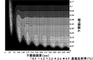
次に、レジスト下層膜のk値が0.2の場合と0.6の場合の、レジスト中間膜とレジスト下層膜の膜厚を変化させたときの反射率変化を図6と図7に示す。 Next, FIGS. 6 and 7 show the reflectance change when the resist intermediate film and the resist underlayer film are changed in thickness when the k value of the resist underlayer film is 0.2 and 0.6. .
図6のk値が0.2のレジスト下層膜は、2層プロセスに最適化されたレジスト下層膜を想定しており、図7のk値が0.6のレジスト下層膜は、波長193nmにおけるノボラックやポリヒドロキシスチレンのk値に近い値である。 The resist underlayer film having a k value of 0.2 in FIG. 6 is assumed to be a resist underlayer film optimized for a two-layer process, and the resist underlayer film having a k value of 0.6 in FIG. The value is close to the k value of novolak and polyhydroxystyrene.
レジスト下層膜の膜厚は基板のトポグラフィーによって変動するが、レジスト中間膜の膜厚はほとんど変動せず、設定した膜厚で塗布できると考えられる。 Although the film thickness of the resist underlayer film varies depending on the topography of the substrate, the film thickness of the resist intermediate film hardly varies, and it can be considered that the resist can be applied with a set film thickness.
ここで、レジスト下層膜のk値が高い方(0.6の場合)が、より薄膜で反射を1%以下に抑えることができる。レジスト下層膜のk値が0.2の場合、膜厚250nmでは反射を1%にするためにレジスト中間膜の膜厚を厚くしなければならない。しかし、このようにレジスト中間膜の膜厚を上げると、レジスト中間膜を加工するときのドライエッチング時に最上層のレジスト膜に対する負荷が大きく、好ましいことではない。 Here, the higher the k value of the resist underlayer film (in the case of 0.6), the reflection can be suppressed to 1% or less with a thinner film. When the k value of the resist underlayer film is 0.2, the film thickness of the resist intermediate film must be increased in order to achieve reflection of 1% at a film thickness of 250 nm. However, increasing the film thickness of the resist intermediate film in this manner is not preferable because the load on the uppermost resist film is large during dry etching when the resist intermediate film is processed.
図6と図7は、露光装置のレンズのNAが0.85のドライ露光の場合の反射であるが、3層プロセス用のレジスト中間膜のn、k値と膜厚を最適化することによって、レジスト下層膜のk値によらずに1%以下の反射率にすることができることが示されている。ところが、液浸リソグラフィーによって投影レンズのNAが1.0を超え、レジストだけでなくレジストの下の反射防止膜に入射する光の角度が浅くなってきている。反射防止膜は、膜自体の吸収だけでなく、光の干渉効果による打ち消しの作用を用いて反射を抑えている。斜めの光は光の干渉効果が小さくなるため、反射が増大する。3層プロセスの膜の中で光の干渉作用を用いて反射防止を行っているのはレジスト中間膜である。レジスト下層膜は干渉作用を用いるには十分に厚いために干渉効果による打ち消し合いによる反射防止効果はない。レジスト下層膜表面からの反射を抑える必要があり、そのためにはレジスト下層膜のk値を0.6より小さく、n値を上層のレジスト中間膜に近い値にしなければならない。k値が小さすぎて透明性が高すぎると、基板からの反射も生じてくるため、液浸露光のNA1.3の場合、k値は0.25〜0.48程度が最適となる。n値は中間膜、下層共にレジストのn値1.7に近い値が目標値となる。 FIGS. 6 and 7 show reflections in the case of dry exposure when the NA of the exposure apparatus lens is 0.85. By optimizing the n, k values and film thickness of the resist intermediate film for the three-layer process, FIG. It is shown that the reflectance can be 1% or less regardless of the k value of the resist underlayer film. However, the NA of the projection lens exceeds 1.0 due to immersion lithography, and the angle of light incident not only on the resist but also on the antireflection film under the resist is becoming shallower. The antireflection film suppresses reflection not only by the absorption of the film itself but also by the action of cancellation due to the light interference effect. Since oblique light has a small light interference effect, reflection increases. Of the three-layer process film, the resist intermediate film is used to prevent reflection by using the interference of light. Since the resist underlayer film is sufficiently thick to use the interference action, there is no antireflection effect due to cancellation by the interference effect. It is necessary to suppress reflection from the surface of the resist underlayer film. For this purpose, the k value of the resist underlayer film must be smaller than 0.6 and the n value must be close to the upper resist intermediate film. When the k value is too small and the transparency is too high, reflection from the substrate also occurs. Therefore, in the case of immersion exposure NA 1.3, the optimum k value is about 0.25 to 0.48. The n value is a target value that is close to the n value 1.7 of the resist for both the intermediate film and the lower layer.
ベンゼン環は吸収が非常に強く、クレゾールノボラックやポリヒドロキシスチレンのk値は0.6を超える。ベンゼン環よりも波長193nmにおける透明性が高く、エッチング耐性が高いものの一つにナフタレン環がある。例えば、特許文献1にナフタレン環、アントラセン環を有するレジスト下層膜が提案されている。我々の測定値では、ナフトール共縮合ノボラック樹脂、ポリビニルナフタレン樹脂のk値は0.3〜0.4の間である。また、ナフトール共縮合ノボラック樹脂、ポリビニルナフタレン樹脂の波長193nmにおけるn値は低く、ナフトール共縮合ノボラック樹脂で1.4、ポリビニルナフタレン樹脂に至っては1.2である。例えば、特許文献2、特許文献3で示されるアセナフチレン重合体においては、193nmにおけるn値は1.5、k値は0.4で目標値に近い。n値が高く、k値が低く透明でかつエッチング耐性が高い下層膜が求められている。
The benzene ring is very strongly absorbed, and the k value of cresol novolac and polyhydroxystyrene exceeds 0.6. One of the higher transparency and higher etching resistance at a wavelength of 193 nm than a benzene ring is a naphthalene ring. For example,
ここで、特許文献4にビスナフトール基を有するレジスト下層膜形成材料が提案されており、n値、k値共に目標値に近く、エッチング耐性に優れる特徴を有している。
Here,
また、下地の被加工基板に段差がある場合、レジスト下層膜によって段差を平坦化させる必要がある。レジスト下層膜を平坦化させることによって、その上に成膜するレジスト中間膜やレジスト上層膜であるフォトレジスト膜の膜厚変動を抑え、リソグラフィーのフォーカスマージンを拡大することができる。 Further, when there is a step in the substrate to be processed, it is necessary to flatten the step with a resist underlayer film. By flattening the resist lower layer film, it is possible to suppress the film thickness variation of the resist intermediate film formed on the resist film and the photoresist film as the resist upper layer film, and to expand the lithography focus margin.
しかし、メタンガス、エタンガス、アセチレンガスなどを原料に用いたCVDによって形成されたアモルファスカーボン下層膜は、段差をフラットに埋め込むことが困難である。一方、レジスト下層膜をスピンコーティングによって形成した場合、基板の凹凸を埋め込むことができる長所がある。また、更に、塗布型の材料に於いて埋め込み特性を向上させるために分子量が低く、分子量分布が広いノボラックを用いる方法、ベースポリマーに低融点の低分子化合物をブレンドする方法が提案されている。 However, it is difficult for the amorphous carbon underlayer film formed by CVD using methane gas, ethane gas, acetylene gas or the like as a raw material to bury the step flatly. On the other hand, when the resist underlayer film is formed by spin coating, there is an advantage that the unevenness of the substrate can be embedded. Further, in order to improve the embedding characteristics in the coating type material, a method using a novolak having a low molecular weight and a wide molecular weight distribution, and a method of blending a low molecular compound having a low melting point with a base polymer have been proposed.
ノボラック樹脂が加熱だけで分子間架橋し硬化することは従来からよく知られている。ここでは、加熱によってクレゾールノボラックのヒドロキシ基にフェノキシラジカルが発生し、共鳴によってノボラック樹脂の連結基のメチレンにラジカルが移動し、メチレン同士が架橋するラジカルカップリングによる架橋メカニズムが報告されている。特許文献5にポリアリーレンやナフトールノボラック、ヒドロキシアントラセンノボラックなどの多環芳香族化合物を熱によって脱水素あるいは脱水縮合反応によって炭素密度を高めた下層膜を用いるパターン形成方法が報告されている。 It has been well known that novolak resins are crosslinked and cured by heating alone. Here, a crosslinking mechanism by radical coupling is reported in which a phenoxy radical is generated in the hydroxy group of cresol novolac by heating, the radical is transferred to methylene of the linking group of the novolak resin by resonance, and the methylenes are cross-linked. Patent Document 5 reports a pattern forming method using a lower layer film in which a polycyclic aromatic compound such as polyarylene, naphthol novolak, hydroxyanthracene novolak, or the like is dehydrogenated by heat or a carbon density is increased by a dehydration condensation reaction.
ガラス状のカーボン膜は800℃以上の加熱によって形成される(非特許文献1)。しかしながら、デバイスダメージやウェハーの変形への影響を考えると、リソグラフィーのウェハープロセスでの加熱できる温度の上限は600℃以下、好ましくは500℃以下である。 A glassy carbon film is formed by heating at 800 ° C. or higher (Non-Patent Document 1). However, considering the influence on device damage and wafer deformation, the upper limit of the heatable temperature in the lithography wafer process is 600 ° C. or less, preferably 500 ° C. or less.
加工線幅の縮小に伴い、レジスト下層膜をマスクに被加工基板をエッチングするときにレジスト下層膜がよれたり曲がったりする現象が起きる事が報告されている(非特許文献2)。フルオロカーボン系のガスによる基板エッチング中に、レジスト下層膜の水素原子がフッ素原子で置換される現象が示されている。レジスト下層膜表面がテフロン(登録商標)化されることによって下層膜の体積増加により膨潤したり、ガラス転移点が低下することによって、より微細なパターンのよれが生じるものと考えられる。前述の文献では、水素含有率の低いレジスト下層膜を適用することによってよれが防止できることが示されている。CVDで作成したアモルファスカーボン膜は、膜中の水素原子を極めて少なくすることができ、よれ防止には非常に有効である。しかしながら、前述のようにCVDは段差の埋め込み特性が悪く、またCVD装置の価格と装置フットプリント面積の占有により導入が困難な場合がある。コーティング、特にスピンコート法で製膜可能な下層膜形成材料でよれの問題を解決することができれば、プロセスと装置の簡略化のメリットは大きい。 It has been reported that with the reduction of the processing line width, a phenomenon occurs in which the resist underlayer film is bent or bent when the substrate to be processed is etched using the resist underlayer film as a mask (Non-patent Document 2). It shows a phenomenon in which hydrogen atoms in a resist underlayer film are replaced with fluorine atoms during substrate etching with a fluorocarbon-based gas. It is considered that the resist underlayer film surface is made Teflon (registered trademark) to swell due to the increase in volume of the underlayer film or the glass transition point is lowered, thereby causing a finer pattern distortion. In the above-mentioned document, it has been shown that twisting can be prevented by applying a resist underlayer film having a low hydrogen content. An amorphous carbon film prepared by CVD can extremely reduce the number of hydrogen atoms in the film and is very effective in preventing dripping. However, as described above, CVD has poor step embedding characteristics and may be difficult to introduce due to the cost of the CVD apparatus and the occupation footprint area. If the problem of dripping can be solved by coating, particularly an underlayer film forming material that can be formed by spin coating, the merit of simplification of the process and the apparatus is great.
レジスト下層膜の上にCVD法でハードマスクを形成するマルチレイヤープロセスが検討されている。シリコン系のハードマスク(珪素酸化膜、珪素窒化膜、珪素窒化酸化膜)の場合に於いてもスピンコート法で形成するハードマスクよりもCVD等で形成した無機ハードマスクの方がエッチング耐性が高い。また、被加工基板が低誘電率膜であり、そこからのフォトレジストへの汚染(ポイゾニング)が生じる場合があるが、CVD膜の方がポイゾニング防止の遮断膜としての効果が高い。 A multi-layer process in which a hard mask is formed on a resist underlayer film by a CVD method has been studied. In the case of silicon hard masks (silicon oxide film, silicon nitride film, silicon oxynitride film), the etching resistance of inorganic hard masks formed by CVD or the like is higher than that of hard masks formed by spin coating. . Further, the substrate to be processed is a low dielectric constant film, and the photoresist may be contaminated (poisoning) from there, but the CVD film is more effective as a blocking film for preventing poisoning.
そこで、平坦化のためにレジスト下層膜をスピンコートで形成し、その上のレジスト中間膜としての無機ハードマスク中間膜をCVD法で作成するプロセスが検討されている。CVD法で無機ハードマスク中間膜を作成する場合、特に窒化物系の膜の作成に於いて最低300℃、通常は400℃の基板の加熱が必要とされる。従って、スピンコート法でレジスト下層膜を作成した場合、400℃の耐熱性が必要であるが、通常のクレゾールノボラック、ナフトールノボラック、および耐熱性が高いフルオレンビスフェノールにおいても400℃の加熱に耐えることができず、加熱後大きな膜減りが生じてしまう。このように、CVD法で無機ハードマスク中間膜を形成する際の高温の加熱にも耐えることができるようなレジスト下層膜が求められている。 Therefore, a process for forming a resist underlayer film by spin coating for planarization and forming an inorganic hard mask intermediate film as a resist intermediate film thereon by a CVD method has been studied. When forming an inorganic hard mask intermediate film by CVD, it is necessary to heat the substrate at a minimum of 300 ° C., usually 400 ° C., particularly in forming a nitride-based film. Therefore, when a resist underlayer film is formed by spin coating, heat resistance of 400 ° C. is necessary, but ordinary cresol novolak, naphthol novolak, and fluorene bisphenol having high heat resistance can withstand heating at 400 ° C. Inability to do so results in significant film loss after heating. Thus, there is a need for a resist underlayer film that can withstand high-temperature heating when forming an inorganic hard mask intermediate film by CVD.
また、このような耐熱性が原因となる加熱後の膜減りや樹脂の劣化の問題から、従来レジスト下層膜形成材料の熱処理は通常300℃以下(好ましくは80〜300℃の範囲内)で行われていた。しかしながら、溶媒処理後に減膜が生じたり、基板のエッチング中にパターンによれが生じてしまうという問題は生じたままであった。 In addition, due to the problem of film loss after heating and deterioration of resin due to such heat resistance, heat treatment of conventional resist underlayer film forming materials is usually performed at 300 ° C. or less (preferably within a range of 80 to 300 ° C.). It was broken. However, there still remains a problem that the film is reduced after the solvent treatment or the pattern is distorted during the etching of the substrate.
以上より、反射防止膜としての最適なn、k値と埋め込み特性、優れたエッチング耐性、耐溶媒性を有し、更にCVD法などによる無機ハードマスク中間膜形成中の高温にも耐えることができる耐熱性を有し、基板のエッチング中によれが生じないレジスト下層膜を形成するための材料及びパターン形成方法が求められているのである。 As described above, it has optimum n and k values and embedding characteristics as an antireflection film, excellent etching resistance and solvent resistance, and can withstand high temperatures during the formation of an inorganic hard mask intermediate film by CVD or the like. There is a need for a material and a pattern forming method for forming a resist underlayer film that has heat resistance and does not sag during etching of the substrate.
トルクセン構造を有するポジ型レジストが提案されている(特許文献6)。ヒドロキシ基を酸不安定基で置換されたトルクセンをベースにしたレジストは、優れたエッチング耐性を有するEB、EUVレジストとして紹介されている。又、エッチング耐性に優れる複数のビスフェノールを有する下層膜形成材料の中で、トルクセンビスフェノール化合物が示されており(特許文献7)、トルクセン化合物が注目されている。 A positive resist having a torquesen structure has been proposed (Patent Document 6). A resist based on torquesen in which a hydroxy group is substituted with an acid labile group has been introduced as an EB or EUV resist having excellent etching resistance. Among the underlayer film forming materials having a plurality of bisphenols having excellent etching resistance, a torquesen bisphenol compound has been shown (Patent Document 7), and a torquesen compound has attracted attention.
本発明は、上記事情に鑑みなされたもので、レジスト下層膜形成材料であって、反射率を低減でき、エッチング耐性が高く、高い耐熱性、耐溶媒性を有し、特に基板のエッチング中によれの発生がないレジスト下層膜を形成するためのレジスト下層膜形成材料及びこれを用いたパターン形成方法を提供することを目的とする。 The present invention has been made in view of the above circumstances, and is a resist underlayer film forming material that can reduce reflectivity, has high etching resistance, has high heat resistance and solvent resistance, and particularly during etching of a substrate. It is an object of the present invention to provide a resist underlayer film forming material for forming a resist underlayer film free from kinking and a pattern forming method using the same.
本発明は、上記課題を解決するためになされたものであって、基板にレジスト下層膜形成材料によりレジスト下層膜を形成し、少なくとも該レジスト下層膜の上にフォトレジスト組成物によりレジスト上層膜を形成し、該レジスト上層膜に露光及び現像を行ってパターンを形成した後、該レジスト上層膜に形成されたパターンをレジスト下層膜に転写して、更に該レジスト下層膜に転写されたパターンを基板に転写することにより基板にパターンを形成する方法において用いるレジスト下層膜形成材料であって、
下記一般式(1)で示される置換又は非置換のナフトール基を有するトルクセン化合物、又は、前記トルクセン化合物とアルデヒド類との縮合反応によってノボラック化した樹脂を含有するものであることを特徴とするレジスト下層膜形成材料を提供する。

A resist comprising a torquesen compound having a substituted or unsubstituted naphthol group represented by the following general formula (1) , or a resin novolakized by a condensation reaction between the torquecene compound and an aldehyde: An underlayer film forming material is provided.
これにより、反射率を低減でき、エッチング耐性が高く、高い耐熱性、耐溶媒性を有し、特に基板のエッチング中によれの発生がないレジスト下層膜を形成するためのレジスト下層膜形成材料となる。 With this, a resist underlayer film forming material for forming a resist underlayer film that can reduce reflectance, has high etching resistance, has high heat resistance and solvent resistance, and does not occur particularly during substrate etching Become.
更に、有機溶剤を含有するものであることが好ましい。また、架橋剤及び酸発生剤を含有するものであることが好ましい。 Furthermore, it preferably contains an organic solvent. Moreover, it is preferable to contain a crosslinking agent and an acid generator.
このように、本発明のレジスト下層膜形成材料は、更に有機溶剤を含有することが好ましく、更に、スピンコート特性、段差基板の埋め込み特性、膜の剛性や耐溶媒性を上げるために、架橋剤及び酸発生剤を含むことが好ましい As described above, the resist underlayer film forming material of the present invention preferably further contains an organic solvent. Further, in order to increase spin coating characteristics, step board embedding characteristics, film rigidity, and solvent resistance, a crosslinking agent is used. And an acid generator
また、本発明では、リソグラフィーにより基板にパターンを形成する方法であって、少なくとも、基板上に前記本発明のレジスト下層膜形成材料を用いてレジスト下層膜を形成し、該レジスト下層膜の上に珪素原子を含有するレジスト中間膜材料を用いてレジスト中間膜を形成し、該レジスト中間膜の上にフォトレジスト組成物であるレジスト上層膜材料を用いてレジスト上層膜を形成して、該レジスト上層膜のパターン回路領域を露光した後、現像液で現像してレジスト上層膜にレジストパターンを形成し、該レジストパターンが形成されたレジスト上層膜をマスクにしてレジスト中間膜をエッチングしてパターンを形成し、該パターンが形成されたレジスト中間膜をマスクにしてレジスト下層膜をエッチングしてパターンを形成し、さらに、該パターンが形成されたレジスト下層膜をマスクにして基板をエッチングして基板にパターンを形成することを特徴とするパターン形成方法を提供する。 Further, the present invention is a method for forming a pattern on a substrate by lithography, wherein at least a resist underlayer film is formed on the substrate using the resist underlayer film forming material of the present invention, and the resist underlayer film is formed on the resist underlayer film. A resist intermediate film is formed using a resist intermediate film material containing silicon atoms, and a resist upper film is formed on the resist intermediate film using a resist upper film material that is a photoresist composition. After the pattern circuit area of the film is exposed, it is developed with a developer to form a resist pattern on the resist upper film, and the resist intermediate film on which the resist pattern is formed is used as a mask to etch the resist intermediate film to form a pattern. Then, using the resist intermediate film on which the pattern is formed as a mask, the resist underlayer film is etched to form a pattern. , A pattern forming method by etching the substrate using the resist underlayer film having the formed pattern as a mask and forming a pattern on a substrate.
このような3層レジストプロセスを用いたパターン形成方法であれば、基板に微細なパターンを高精度で形成することができる。 With such a pattern formation method using a three-layer resist process, a fine pattern can be formed on the substrate with high accuracy.
さらに、本発明では、リソグラフィーにより基板にパターンを形成する方法であって、少なくとも、基板上に前記本発明のレジスト下層膜形成材料を用いてレジスト下層膜を形成し、該レジスト下層膜の上に珪素酸化膜、珪素窒化膜、及び珪素酸化窒化膜のいずれかからなる無機ハードマスク中間膜を形成し、該無機ハードマスク中間膜の上にフォトレジスト組成物であるレジスト上層膜材料を用いてレジスト上層膜を形成して、該レジスト上層膜のパターン回路領域を露光した後、現像液で現像してレジスト上層膜にレジストパターンを形成し、該レジストパターンが形成されたレジスト上層膜をマスクにして無機ハードマスク中間膜をエッチングしてパターンを形成し、該パターンが形成された無機ハードマスク中間膜をマスクにしてレジスト下層膜をエッチングしてパターンを形成し、さらに、該パターンが形成されたレジスト下層膜をマスクにして基板をエッチングして基板にパターンを形成することを特徴とするパターン形成方法を提供する。 Furthermore, the present invention is a method for forming a pattern on a substrate by lithography, wherein at least a resist underlayer film is formed on the substrate using the resist underlayer film forming material of the present invention, and the resist underlayer film is formed on the resist underlayer film. An inorganic hard mask intermediate film made of any one of a silicon oxide film, a silicon nitride film, and a silicon oxynitride film is formed, and a resist upper layer film material that is a photoresist composition is formed on the inorganic hard mask intermediate film by using a resist upper layer film material. After forming the upper layer film and exposing the pattern circuit region of the resist upper layer film, developing with a developer to form a resist pattern on the resist upper layer film, and using the resist upper layer film on which the resist pattern is formed as a mask The inorganic hard mask intermediate film is etched to form a pattern, and the inorganic hard mask intermediate film on which the pattern is formed is used as a mask. Strike underlayer film to form an etching to pattern, furthermore, a pattern forming method by etching the substrate using the resist underlayer film having the formed pattern as a mask and forming a pattern on a substrate.
このようにレジスト下層膜の上にレジスト中間膜として無機ハードマスクを形成する際、本発明のレジスト下層膜形成材料を用いると、無機ハードマスク中間膜形成時の高温処理にも耐えうる高い耐熱性を有するレジスト下層膜を用いたパターン形成方法とできる。 Thus, when forming an inorganic hard mask as a resist intermediate film on the resist underlayer film, the use of the resist underlayer film forming material of the present invention provides high heat resistance that can withstand high-temperature processing during the formation of the inorganic hard mask intermediate film. A pattern forming method using a resist underlayer film having
また、本発明では、リソグラフィーにより基板にパターンを形成する方法であって、少なくとも、基板上に前記本発明のレジスト下層膜形成材料を用いてレジスト下層膜を形成し、該レジスト下層膜の上に珪素酸化膜、珪素窒化膜、及び珪素酸化窒化膜のいずれかからなる無機ハードマスク中間膜を形成し、該無機ハードマスク中間膜の上に有機反射防止膜(BARC)を形成し、該BARC上にフォトレジスト組成物であるレジスト上層膜材料を用いてレジスト上層膜を形成して4層レジスト膜とし、レジスト上層膜のパターン回路領域を露光した後、現像液で現像してレジスト上層膜にレジストパターンを形成し、該レジストパターンが形成されたレジスト上層膜をマスクにしてBARC膜及び無機ハードマスク中間膜をエッチングして無機ハードマスク中間膜にパターンを形成し、該パターンが形成された無機ハードマスク中間膜をマスクにしてレジスト下層膜をエッチングしてパターンを形成し、さらに、該パターンが形成されたレジスト下層膜をマスクにして基板をエッチングして基板にパターンを形成することを特徴とするパターン形成方法を提供する。 Further, the present invention is a method for forming a pattern on a substrate by lithography, wherein at least a resist underlayer film is formed on the substrate using the resist underlayer film forming material of the present invention, and the resist underlayer film is formed on the resist underlayer film. An inorganic hard mask intermediate film made of any one of a silicon oxide film, a silicon nitride film, and a silicon oxynitride film is formed, an organic antireflection film (BARC) is formed on the inorganic hard mask intermediate film, and the BARC The resist upper layer film material, which is a photoresist composition, is used to form a resist upper layer film to form a four-layer resist film, the pattern circuit region of the resist upper layer film is exposed, and then developed with a developing solution to form a resist on the resist upper layer film. A pattern is formed, and the BARC film and the inorganic hard mask intermediate film are etched using the resist upper layer film on which the resist pattern is formed as a mask. Forming a pattern on the hard mask intermediate film, etching the resist lower layer film using the inorganic hard mask intermediate film on which the pattern is formed as a mask to form a pattern, and further forming a resist lower layer film on which the pattern is formed There is provided a pattern forming method, wherein a pattern is formed on a substrate by etching the substrate using a mask.
このように、本発明の方法では無機ハードマスク中間膜とレジスト上層膜の間に有機反射防止膜を形成することができる。 Thus, in the method of the present invention, an organic antireflection film can be formed between the inorganic hard mask intermediate film and the resist upper layer film.
また、前記無機ハードマスク中間膜の形成において、CVD法又はALD法により、珪素酸化膜、珪素窒化膜、及び珪素酸化窒化膜のいずれかからなる無機ハードマスク中間膜を形成することが好ましい。 In forming the inorganic hard mask intermediate film, it is preferable to form an inorganic hard mask intermediate film made of any one of a silicon oxide film, a silicon nitride film, and a silicon oxynitride film by a CVD method or an ALD method.
このように、無機ハードマスク中間膜をCVD法あるいはALD法により形成することにより、エッチング耐性を高くすることができる。 As described above, the etching resistance can be increased by forming the inorganic hard mask intermediate film by the CVD method or the ALD method.
さらに、前記レジスト上層膜の形成において、珪素原子を含有するポリマーを含まない前記フォトレジスト組成物である前記レジスト上層膜材料を用いて前記レジスト上層膜を形成し、
前記レジスト下層膜のエッチングにおいて、前記パターンが形成されたレジスト中間膜又は前記パターンが形成された無機ハードマスク中間膜をマスクにして前記レジスト下層膜を酸素ガス又は水素ガスを主体とするエッチングガスによりエッチングすることが好ましい。
Furthermore, in the formation of the resist upper layer film, the resist upper layer film is formed using the resist upper layer film material which is the photoresist composition not including a polymer containing silicon atoms,
In the etching of the resist underlayer film, the resist underlayer film is etched with an etching gas mainly composed of oxygen gas or hydrogen gas using the resist intermediate film in which the pattern is formed or the inorganic hard mask intermediate film in which the pattern is formed as a mask. Etching is preferred.
このように、無機ハードマスク中間膜パターンをエッチングマスクにしてレジスト下層膜をエッチングする際、珪素原子を含む無機ハードマスクは、酸素ガス又は水素ガスによるエッチング耐性を示すために好ましい。 As described above, when the resist underlayer film is etched using the inorganic hard mask intermediate film pattern as an etching mask, an inorganic hard mask containing silicon atoms is preferable in order to exhibit etching resistance by oxygen gas or hydrogen gas.
以上説明したように、本発明のレジスト下層膜形成材料であれば、反射率を低減でき、エッチング耐性が高く、高い耐熱性、耐溶媒性を有し、特に基板のエッチング中によれの発生がないレジスト下層膜を形成することができる。特に、本発明のレジスト下層膜形成材料を3層以上の多層レジストプロセスに用いることにより、反射防止膜としての最適なn、k値と埋め込み特性、優れたエッチング耐性を有し、高い耐熱性、耐溶媒性を有し、ベーク中のアウトガスの発生を抑制でき、特には60nmよりも細い高アスペクトラインにおける基板のエッチング中によれが生じないレジスト下層膜を形成することが可能となる。 As described above, the resist underlayer film forming material of the present invention can reduce reflectivity, has high etching resistance, has high heat resistance and solvent resistance, and is particularly susceptible to wobbling during substrate etching. A resist underlayer film can be formed. In particular, by using the resist underlayer film forming material of the present invention in a multilayer resist process of three or more layers, it has optimum n, k value and embedding characteristics as an antireflection film, excellent etching resistance, high heat resistance, It is possible to form a resist underlayer film that has solvent resistance, can suppress the generation of outgas during baking, and in particular does not occur during etching of the substrate in a high aspect line narrower than 60 nm.
更に、本発明のパターン形成方法であれば、基板に微細なパターンを高精度で形成することができる。特に、遠紫外線、KrFエキシマレーザー光(248nm)、ArFエキシマレーザー光(193nm)、F2レーザー光(157nm)、Kr2レーザー光(146nm)、Ar2レーザー光(126nm)、軟X線(EUV、13.5nm)、電子線(EB)、X線露光等に好適なパターン形成方法となる。また、本発明のレジスト下層膜形成材料は、CVD法等による無機ハードマスク中間膜形成時の高温処理にも耐えうる高い耐熱性を有するレジスト下層膜を形成できるため、スピンコート法等で得られたレジスト下層膜とCVD法等で得られた無機ハードマスクを組み合わせたパターン形成方法を提供することができる。 Furthermore, according to the pattern forming method of the present invention, a fine pattern can be formed on the substrate with high accuracy. In particular, deep ultraviolet rays, KrF excimer laser light (248 nm), ArF excimer laser light (193 nm), F 2 laser light (157 nm), Kr 2 laser light (146 nm), Ar 2 laser light (126 nm), soft X-rays (EUV) 13.5 nm), electron beam (EB), X-ray exposure, and the like. In addition, the resist underlayer film forming material of the present invention can be obtained by a spin coat method or the like because it can form a resist underlayer film having high heat resistance that can withstand high-temperature treatment when forming an inorganic hard mask intermediate film by a CVD method or the like. It is possible to provide a pattern forming method in which a resist underlayer film and an inorganic hard mask obtained by a CVD method or the like are combined.
以下、本発明についてより詳細に説明する。前述のように、少なくとも3層を有する多層レジスト膜のレジスト下層膜の形成方法として、優れた反射防止膜機能とエッチング耐性、耐熱性、耐溶媒性、埋め込み特性を有し、特に基板のエッチング中によれが生じないレジスト下層膜の形成方法が望まれていた。 Hereinafter, the present invention will be described in more detail. As described above, as a method for forming a resist underlayer film of a multilayer resist film having at least three layers, it has an excellent antireflection film function and etching resistance, heat resistance, solvent resistance, and embedding characteristics, particularly during etching of a substrate. There has been a demand for a method of forming a resist underlayer film that does not sag.
エッチング中パターンよれの低減には、下層膜中の水素原子の低減と、300℃以上の高温ベークが有効とされてきた。 To reduce pattern distortion during etching, reduction of hydrogen atoms in the lower layer film and high-temperature baking at 300 ° C. or higher have been effective.
本発明者は、上記目的を達成するため鋭意検討を行った結果、下記一般式(1)に示されるナフトール基を有するトルクセン化合物は、架橋性が高く加熱によって硬い膜を形成でき、耐熱性が非常に高いことを見出し、300℃以上の高温でベークをすると熱分解を起こさずに溶媒等の蒸発が促進される性質を持ち、透明性が高く、エッチング耐性に優れ、特にはエッチング後の微細パターンのよれ防止効果に優れ、レジスト下層膜として有望な材料であることを見出した。 As a result of intensive studies to achieve the above object, the present inventor has found that the torquecene compound having a naphthol group represented by the following general formula (1) has a high crosslinkability and can form a hard film by heating, and has high heat resistance. Found to be very high and baked at a high temperature of 300 ° C. or higher, it has the property of evaporating solvents without causing thermal decomposition, high transparency, excellent etching resistance, especially fineness after etching The present inventors have found that the material is excellent in the effect of preventing pattern distortion and is a promising material as a resist underlayer film.
即ち、本発明のレジスト下層膜形成材料は、図1に示すように、基板1上の被加工層2にレジスト下層膜形成材料によりレジスト下層膜3を形成し、少なくとも該レジスト下層膜3の上にフォトレジスト組成物によりレジスト上層膜5を形成し、該レジスト上層膜5に露光及び現像を行ってパターンを形成した後、該レジスト上層膜5に形成されたパターンを前記レジスト下層膜3に転写して、更に該レジスト下層膜3に転写されたパターンを被加工層2に転写することにより被加工層2にパターンを形成する方法において用いるレジスト下層膜形成材料であって、下記一般式(1)で示される置換又は非置換のナフトール基を有するトルクセン化合物、又は、前記トルクセン化合物とアルデヒド類との縮合反応によってノボラック化した樹脂を含有するものであることを特徴とするレジスト下層膜形成材料である。
特に、本発明のレジスト下層膜形成材料は、図1のようにレジスト中間膜4を形成する3層プロセスパターン形成方法に好適に用いることのできるレジスト下層膜形成材料として、特に波長300nm以下の高エネルギー線、具体的には248nm、193nm、157nmのエキシマレーザー、3〜20nmの軟X線、電子ビーム、X線におけるエッチング耐性に優れ、透明性が高いものとなる。
In particular, the resist underlayer film forming material of the present invention is particularly suitable as a resist underlayer film forming material that can be suitably used in a three-layer process pattern forming method for forming a resist
また、本発明のレジスト下層膜形成材料は、(A)上記一般式(1)で示される置換又は非置換のナフトール基を有するトルクセン化合物、又は、前記トルクセン化合物とアルデヒド類との縮合反応によってノボラック化した樹脂を必須成分とし、更に(B)有機溶剤を含むことができるものであるが、スピンコート特性、段差基板の埋め込み特性、膜の剛性や耐溶媒性を上げるために(C)ベースポリマー、(D)架橋剤、及び(E)酸発生剤を加えても良い。 Further, the resist underlayer film forming material of the present invention comprises (A) a novolak by a condensation reaction of a torquesen compound having a substituted or unsubstituted naphthol group represented by the general formula (1) or the torquesen compound and aldehydes. the phased resin as essential components, further (B) but is capable of containing an organic solvent, spin-coating property, filling property of the stepped substrate, in order to increase the rigidity and solvent resistance of the film (C) a base polymer , (D) a crosslinking agent, and (E) an acid generator may be added.
一般式(1)中、R1、R4、R7、R10、R11、及びR12は、それぞれ、同一又は異種の、水素原子、炭素数1〜10の直鎖状、分岐状、若しくは環状のアルキル基、炭素数6〜10のアリール基、炭素数2〜10のアルケニル基、ヒドロキシ基、アルコキシ基、アシロキシ基、シアノ基、ニトロ基、アミノ基、又はハロゲン原子である。アルコキシ基としては直鎖状、分岐状、若しくは環状の炭素数2〜10のアルコキシ基が好ましく、アシロキシ基としては直鎖状、分岐状、若しくは環状の炭素数2〜10のアシロキシ基が好ましい。 In general formula (1), R 1 , R 4 , R 7 , R 10 , R 11 , and R 12 are the same or different and each represents a hydrogen atom, a linear or branched chain having 1 to 10 carbon atoms, Alternatively, a cyclic alkyl group, an aryl group having 6 to 10 carbon atoms, an alkenyl group having 2 to 10 carbon atoms, a hydroxy group, an alkoxy group, an acyloxy group, a cyano group, a nitro group, an amino group, or a halogen atom. The alkoxy group is preferably a linear, branched, or cyclic alkoxy group having 2 to 10 carbon atoms, and the acyloxy group is preferably a linear, branched, or cyclic acyloxy group having 2 to 10 carbon atoms.
また、R2、R5、及びR8は、それぞれ、同一又は異種の、水素原子、炭素数1〜6の直鎖状、分岐状、環状のアルキル基、アシル基、グリシジル基、又は酸不安定基である。アシル基としては直鎖状、分岐状、若しくは環状の炭素数2〜10のアシル基が好ましく、酸不安定基としてはメトキシメチル、エトキシエチル、t−ブチル、t−ブトキシカルボニルなどが好ましい。 R 2 , R 5 , and R 8 are the same or different and each represents a hydrogen atom, a linear, branched, or cyclic alkyl group having 1 to 6 carbon atoms, an acyl group, a glycidyl group, or an acid group. It is a stable group. The acyl group is preferably a linear, branched or cyclic acyl group having 2 to 10 carbon atoms, and the acid labile group is preferably methoxymethyl, ethoxyethyl, t-butyl, t-butoxycarbonyl or the like.
一般式(1)中、R3、R6、及びR9は、同一又は異種の、水素原子、ヒドロキシ基、炭素数1〜10の直鎖状、分岐状、若しくは環状のアルキル基、アルコキシ基、炭素数2〜10のアルケニル基、炭素数2〜10のアルキニル基、又は炭素数6〜20のアリール基である。また、p、q、rは1〜6の整数である。アルコキシ基としては炭素数1〜10の直鎖状、分岐状、若しくは環状のアルコキシ基が好ましい。なお、R3、R6、及びR9で示されるアルキル基、アルコキシ基、アルケニル基、アルキニル基、又はアリール基はそれぞれ水素原子が、ヒドロキシル基等で置換されたものであっても良い。 In general formula (1), R 3 , R 6 , and R 9 are the same or different, a hydrogen atom, a hydroxy group, a linear, branched, or cyclic alkyl group having 1 to 10 carbon atoms, or an alkoxy group. , An alkenyl group having 2 to 10 carbon atoms, an alkynyl group having 2 to 10 carbon atoms, or an aryl group having 6 to 20 carbon atoms. P, q, and r are integers of 1-6. The alkoxy group is preferably a linear, branched or cyclic alkoxy group having 1 to 10 carbon atoms. The alkyl group, alkoxy group, alkenyl group, alkynyl group, or aryl group represented by R 3 , R 6 , and R 9 may have a hydrogen atom substituted with a hydroxyl group or the like.
上記一般式(1)に示される置換又は非置換のナフトール基を有するトルクセン化合物は、炭素の割合が高く優れたエッチング耐性と溶解性と架橋硬化特性を有する。トルクセンは平面構造であるために、密度高く積層させることができる。これによってエッチング耐性を高めることができる。ビスナフトールとトルクセンの結合部分は4級炭素のカルド構造を有するために、これによってもエッチング耐性が高くなる。更には、ナフトールが分子の外側を向いているので、架橋反応性が高く、架橋密度が高い剛直な膜を形成することができる。トルクセンは、インダノンを酸の存在下加熱することによって3分子が縮合して合成される。トルクセンを酸化させることによってトルクセノンを合成し、カルボニル基をナフトールと反応してナフトール置換のトルクセン化合物を合成することができる。また、インダノンの代わりに1、3−ジオキソインダンを用いて3分子を縮合すると、1段階でトルクセノンを合成できる。 The torquecene compound having a substituted or unsubstituted naphthol group represented by the general formula (1) has a high carbon ratio and excellent etching resistance, solubility, and cross-linking curing characteristics. Torque Sen has a planar structure and can be laminated with high density. This can increase the etching resistance. The bonding portion between bisnaphthol and torquesen has a quaternary carbon cardo structure, which also increases etching resistance. Furthermore, since naphthol faces the outside of the molecule, it is possible to form a rigid film having high crosslinking reactivity and high crosslinking density. Torxene is synthesized by condensing three molecules by heating indanone in the presence of an acid. Torxenone is synthesized by oxidizing torquesen, and a naphthol-substituted torquecene compound can be synthesized by reacting a carbonyl group with naphthol. In addition, when 3 molecules are condensed using 1,3-dioxoindane instead of indanone, torquesenone can be synthesized in one step.
一般式(1)に示される置換又は非置換のナフトール基を有するトルクセン化合物は、具体的には下記に例示することができる。 Specific examples of the torquecene compound having a substituted or unsubstituted naphthol group represented by the general formula (1) can be given below.
一般式(1)で示される置換又は非置換のナフトール基を有するトルクセン化合物は、ヒドロキシ基が分子の外側に向いているため、隣の分子との架橋反応の反応性が高く、熱による硬化後硬い皮膜を形成でき、ベーク中に発生するアウトガス成分が少ない。また、硬い膜はエッチング中のよれが起きにくいメリットがある。さらに、このトルクセン化合物は溶剤への溶解性が高く、ポリマーではないので埋め込み特性に優れるというメリットがある。一方、ヒドロキシ基が内側を向いているカリックスアレーンやカリックスレゾルシンは架橋性や溶解性に乏しく、レジスト下層膜としての適用は難しい。 The torquesen compound having a substituted or unsubstituted naphthol group represented by the general formula (1) has a high reactivity of the crosslinking reaction with an adjacent molecule because the hydroxy group is directed to the outside of the molecule. A hard film can be formed, and there are few outgas components generated during baking. In addition, a hard film has an advantage that it is difficult to cause kinking during etching. Furthermore, this torquesen compound is highly soluble in a solvent and has the merit of excellent embedding characteristics because it is not a polymer. On the other hand, calixarene and calixresorcin having a hydroxy group facing inward are poor in crosslinkability and solubility, and are difficult to apply as a resist underlayer film.
一般式(1)で示される置換又は非置換のナフトール基を有するトルクセン化合物は、4級炭素を有し、また炭素の割合が90%前後の高い値となりうるために非常に高い耐熱性を有する。一般に、レジスト下層膜上にCVD法あるいはALD法等により珪素酸化膜、珪素窒化膜、及び珪素窒化酸化膜等のいずれかの無機ハードマスク中間膜を形成する場合、特に窒化膜系の膜に於いては300℃以上の高温が必要であり、レジスト下層膜としても高耐熱性が要求される。また、ナフトールを有するトルクセン化合物は、ベンゼン環の縮合炭化水素であるために吸収シフトによって波長193nmにおける吸収が比較的小さく、3層プロセスを用いたときに特に100nm以上の膜厚で良好な反射防止効果が期待される。また、ナフトールを有するトルクセン化合物は、通常のm−クレゾールノボラック樹脂よりも、基板加工に用いられるCF4/CHF3ガス及びCl2/BCl3系ガスエッチングに対するエッチング耐性が高く、芳香族の数が増えた分だけ水素原子が減ってエッチング耐性、とりわけエッチング中のパターンよれの発生を抑えることができる。更に300℃を越える温度でベークをすることによって、さらに高いエッチング耐性、耐溶媒性を有し、基板エッチング中のパターンよれの発生を抑えることができるものとなる。 The torquesen compound having a substituted or unsubstituted naphthol group represented by the general formula (1) has a quaternary carbon and has a very high heat resistance because the carbon ratio can be as high as about 90%. . In general, when an inorganic hard mask intermediate film such as a silicon oxide film, a silicon nitride film, or a silicon oxynitride film is formed on a resist underlayer film by a CVD method or an ALD method, particularly in a nitride film. In this case, a high temperature of 300 ° C. or higher is required, and high heat resistance is required as a resist underlayer film. In addition, since the torquesen compound having naphthol is a condensed hydrocarbon of a benzene ring, absorption at a wavelength of 193 nm is relatively small due to an absorption shift, and good antireflection at a film thickness of 100 nm or more when using a three-layer process. Expected to be effective. In addition, the torquesen compound having naphthol has higher etching resistance to CF 4 / CHF 3 gas and Cl 2 / BCl 3 gas etching used for substrate processing than ordinary m-cresol novolac resins, and has a higher number of aromatics. Hydrogen atoms are reduced by the increased amount, and etching resistance, particularly generation of pattern distortion during etching can be suppressed. Further, by baking at a temperature exceeding 300 ° C., the film has higher etching resistance and solvent resistance, and the occurrence of pattern distortion during substrate etching can be suppressed.
カルボニル基を有する化合物をナフトールと反応させてビスナフトール基を有する化合物を合成する方法が特開2007−99741号に示されている。ここではフルオレノンとナフトールを酸触媒の存在下で反応させてフルオレンビスナフトールを合成する方法が示されている。トルクセノンとナフトールとの反応も同様の方法を適用させることができる。 Japanese Patent Application Laid-Open No. 2007-99741 discloses a method of synthesizing a compound having a bisnaphthol group by reacting a compound having a carbonyl group with naphthol. Here, a method of synthesizing fluorene bisnaphthol by reacting fluorenone and naphthol in the presence of an acid catalyst is shown. A similar method can be applied to the reaction between torquesenone and naphthol.
この場合のナフトール類としては、1−ナフトール、2−ナフトール、2−メチル−1−ナフトール、4−メトキシ−1−ナフトール、7−メトキシ−2−ナフトール及び1,5−ジヒドロキシナフタレン、1,7−ジヒドロキシナフタレン、2,6−ジヒドロキシナフタレン、2,7−ジヒドロキシナフタレン等のジヒドロキシナフタレン、1,2,4−トリヒドロキシナフタレン、1,3,8−トリヒドロキシナフタレン等のトリヒドロキシナフタレンが挙げられる。これらのナフトール類は単独又は2種以上を組み合わせても良い。 In this case, naphthols include 1-naphthol, 2-naphthol, 2-methyl-1-naphthol, 4-methoxy-1-naphthol, 7-methoxy-2-naphthol and 1,5-dihydroxynaphthalene, 1,7 Examples include dihydroxynaphthalene such as -dihydroxynaphthalene, 2,6-dihydroxynaphthalene, and 2,7-dihydroxynaphthalene, and trihydroxynaphthalene such as 1,2,4-trihydroxynaphthalene and 1,3,8-trihydroxynaphthalene. These naphthols may be used alone or in combination of two or more.
本発明のレジスト下層膜形成材料には、更に、上記一般式(1)で示されるようなナフトール基を有するトルクセン化合物とアルデヒド類との縮合反応によってノボラック化した樹脂も含有することができる。 The resist underlayer film forming material of the present invention may further contain a resin that has been novolakized by a condensation reaction between a torquecene compound having a naphthol group and an aldehyde as represented by the general formula (1).
ここで用いられるアルデヒド類としては、例えばホルムアルデヒド、トリオキサン、パラホルムアルデヒド、ベンズアルデヒド、アセトアルデヒド、プロピルアルデヒド、フェニルアセトアルデヒド、α−フェニルプロピルアルデヒド、β−フェニルプロピルアルデヒド、o−ヒドロキシベンズアルデヒド、m−ヒドロキシベンズアルデヒド、p−ヒドロキシベンズアルデヒド、o−クロロベンズアルデヒド、m−クロロベンズアルデヒド、p−クロロベンズアルデヒド、o−ニトロベンズアルデヒド、m−ニトロベンズアルデヒド、p−ニトロベンズアルデヒド、o−メチルベンズアルデヒド、m−メチルベンズアルデヒド、p−メチルベンズアルデヒド、p−エチルベンズアルデヒド、p−n−ブチルベンズアルデヒド、1−ナフタアルデヒド、2−ナフタアルデヒド、フルフラール等を挙げることができる。また、これらのうち、特にホルムアルデヒドを好適に用いることができる。 Examples of aldehydes used here include formaldehyde, trioxane, paraformaldehyde, benzaldehyde, acetaldehyde, propylaldehyde, phenylacetaldehyde, α-phenylpropylaldehyde, β-phenylpropylaldehyde, o-hydroxybenzaldehyde, m-hydroxybenzaldehyde, p. -Hydroxybenzaldehyde, o-chlorobenzaldehyde, m-chlorobenzaldehyde, p-chlorobenzaldehyde, o-nitrobenzaldehyde, m-nitrobenzaldehyde, p-nitrobenzaldehyde, o-methylbenzaldehyde, m-methylbenzaldehyde, p-methylbenzaldehyde, p -Ethylbenzaldehyde, pn-butylbenzaldehyde, 1-naphthalde And hydride, 2-naphthalaldehyde, furfural and the like. Of these, formaldehyde can be particularly preferably used.
これらのアルデヒド類は、単独で又は2種以上を組み合わせて用いることができる。上記アルデヒド類の使用量は、ナフトール基を有するトルクセン化合物1モルに対して0.2〜5モルが好ましく、より好ましくは0.5〜2モルである。 These aldehydes can be used alone or in combination of two or more. The amount of the aldehyde used is preferably 0.2 to 5 mol, and more preferably 0.5 to 2 mol, with respect to 1 mol of the torquecene compound having a naphthol group.
ナフトール基を有するトルクセン化合物とアルデヒド類の縮合反応に触媒を用いることもできる。具体的には塩酸、硝酸、硫酸、ギ酸、シュウ酸、酢酸、メタンスルホン酸、カンファースルホン酸、トシル酸、トリフルオロメタンスルホン酸等の酸性触媒を挙げることができる。 A catalyst can also be used in the condensation reaction of a torquecene compound having a naphthol group and an aldehyde. Specific examples include acidic catalysts such as hydrochloric acid, nitric acid, sulfuric acid, formic acid, oxalic acid, acetic acid, methanesulfonic acid, camphorsulfonic acid, tosylic acid, and trifluoromethanesulfonic acid.
これらの酸性触媒の使用量は、ビスナフトール化合物1モルに対して1×10⁻⁵〜5×10⁻¹モルである。インデン、ヒドロキシインデン、ベンゾフラン、ヒドロキシアントラセン、アセナフチレン、ビフェニル、ビスフェノール、トリスフェノール、ジシクロペンタジエン、テトラヒドロインデン、4−ビニルシクロヘキセン、ノルボルナジエン、5−ビニルノルボルナ−2−エン、α−ピネン、β−ピネン、リモネンなどの非共役2重結合を有する化合物との共重合反応の場合は、必ずしもアルデヒド類は必要ない。 The usage-amount of these acidic catalysts is 1 * 10 < -5 > -5 * 10 < -1 > mol with respect to 1 mol of bisnaphthol compounds. Indene, hydroxyindene, benzofuran, hydroxyanthracene, acenaphthylene, biphenyl, bisphenol, trisphenol, dicyclopentadiene, tetrahydroindene, 4-vinylcyclohexene, norbornadiene, 5-vinylnorborna-2-ene, α-pinene, β-pinene, limonene In the case of a copolymerization reaction with a compound having a non-conjugated double bond such as aldehydes, aldehydes are not necessarily required.
重縮合における反応溶媒として水、メタノール、エタノール、プロパノール、ブタノール、テトラヒドロフラン、ジオキサン又はこれらの混合溶媒を用いることができる。 Water, methanol, ethanol, propanol, butanol, tetrahydrofuran, dioxane or a mixed solvent thereof can be used as a reaction solvent in the polycondensation.
これらの溶媒は、反応原料100質量部に対して0〜2,000質量部の範囲である。反応温度は、反応原料の反応性に応じて適宜選択することができるが、通常10〜200℃の範囲である。 These solvents are in the range of 0 to 2,000 parts by mass with respect to 100 parts by mass of the reaction raw material. Although reaction temperature can be suitably selected according to the reactivity of the reaction raw material, it is the range of 10-200 degreeC normally.
重縮合反応方法としては、ナフトール基を有するトルクセン化合物、アルデヒド類、触媒を一括で仕込む方法や、触媒存在下でナフトール基を有するトルクセン化合物にアルデヒド類を滴下していく方法がある。 As the polycondensation reaction method, there are a method in which a torquecene compound having a naphthol group, an aldehyde, and a catalyst are charged together, and a method in which an aldehyde is added dropwise to a torquecene compound having a naphthol group in the presence of the catalyst.
重縮合反応終了後、系内に存在する未反応原料、触媒等を除去するために、反応釜の温度を130〜230℃にまで上昇させ、1〜50mmHg程度で揮発分を除去することができる。 After completion of the polycondensation reaction, in order to remove unreacted raw materials, catalysts, etc. existing in the system, the temperature of the reaction kettle can be raised to 130-230 ° C., and volatile matter can be removed at about 1-50 mmHg. .
なお、上記一般式(1)に示されるナフトール基を有するトルクセン化合物を単独で重合してもよいが、他のフェノール類を共重合してもよい。 The torquecene compound having a naphthol group represented by the general formula (1) may be polymerized alone, but other phenols may be copolymerized.
このような共重合可能なフェノール類は、フェノール、o−クレゾール、m−クレゾール、p−クレゾール、2,3−ジメチルフェノール、2,5−ジメチルフェノール、3,4−ジメチルフェノール、3,5−ジメチルフェノール、2,4−ジメチルフェノール、2,6−ジメチルフェノール、2,3,5−トリメチルフェノール、3,4,5−トリメチルフェノール、2−t−ブチルフェノール、3−t−ブチルフェノール、4−t−ブチルフェノール、2−フェニルフェノール、3−フェニルフェノール、4−フェニルフェノール、3,5−ジフェニルフェノール、2−ナフチルフェノール、3−ナフチルフェノール、4−ナフチルフェノール、4−トリチルフェノール、レゾルシノール、2−メチルレゾルシノール、4−メチルレゾルシノール、5−メチルレゾルシノール、カテコール、4−t−ブチルカテコール、2−メトキシフェノール、3−メトキシフェノール、2−プロピルフェノール、3−プロピルフェノール、4−プロピルフェノール、2−イソプロピルフェノール、3−イソプロピルフェノール、4−イソプロピルフェノール、2−メトキシ−5−メチルフェノール、2−t−ブチル−5−メチルフェノール、ピロガロール、チモール、イソチモール等を挙げることができる。 Such copolymerizable phenols include phenol, o-cresol, m-cresol, p-cresol, 2,3-dimethylphenol, 2,5-dimethylphenol, 3,4-dimethylphenol, 3,5- Dimethylphenol, 2,4-dimethylphenol, 2,6-dimethylphenol, 2,3,5-trimethylphenol, 3,4,5-trimethylphenol, 2-t-butylphenol, 3-t-butylphenol, 4-t -Butylphenol, 2-phenylphenol, 3-phenylphenol, 4-phenylphenol, 3,5-diphenylphenol, 2-naphthylphenol, 3-naphthylphenol, 4-naphthylphenol, 4-tritylphenol, resorcinol, 2-methyl Resorcinol, 4-methylreso Sinol, 5-methylresorcinol, catechol, 4-t-butylcatechol, 2-methoxyphenol, 3-methoxyphenol, 2-propylphenol, 3-propylphenol, 4-propylphenol, 2-isopropylphenol, 3-isopropylphenol 4-isopropylphenol, 2-methoxy-5-methylphenol, 2-t-butyl-5-methylphenol, pyrogallol, thymol, and isothymol.
その他、共重合可能なモノマーを共重合させることができ、具体的には1−ナフトール、2−ナフトール、2−メチル−1−ナフトール、4−メトキシ−1−ナフトール、7−メトキシ−2−ナフトール及び1,5−ジヒドロキシナフタレン、1,7−ジヒドロキシナフタレン、2,6−ジヒドロキシナフタレン等のジヒドロキシナフタレン、3−ヒドロキシ−ナフタレン−2−カルボン酸メチル、4−トリチルフェノール、インデン、ヒドロキシインデン、ベンゾフラン、ヒドロキシアントラセン、ジヒドロキシアントラセン、トリヒドロキシアントラセン、ヒドロキシピレン、アセナフチレン、ビフェニル、ビスフェノール、トリスフェノール、ジシクロペンタジエン、テトラヒドロインデン、4−ビニルシクロヘキセン、ノルボルナジエン、5−ビニルノルボルナ−2−エン、α−ピネン、β−ピネン、リモネン、フルオレンビスフェノール、フルオレンビスナフトールなどが挙げられ、これらのものを加えた3元以上の共重合体であっても構わない。 In addition, copolymerizable monomers can be copolymerized. Specifically, 1-naphthol, 2-naphthol, 2-methyl-1-naphthol, 4-methoxy-1-naphthol, 7-methoxy-2-naphthol And 1,5-dihydroxynaphthalene, 1,7-dihydroxynaphthalene, dihydroxynaphthalene such as 2,6-dihydroxynaphthalene, methyl 3-hydroxy-naphthalene-2-carboxylate, 4-tritylphenol, indene, hydroxyindene, benzofuran, Hydroxyanthracene, dihydroxyanthracene, trihydroxyanthracene, hydroxypyrene, acenaphthylene, biphenyl, bisphenol, trisphenol, dicyclopentadiene, tetrahydroindene, 4-vinylcyclohexene, norbornadi Emissions, 5 Binirunoruboruna-2-ene, alpha-pinene, beta-pinene, limonene, Furuorenbi scan phenol, etc. Furuorenbi scan naphthol and the like, it may also be a ternary or more copolymer added these things Absent.
以上のようにして合成されたノボラック樹脂のポリスチレン換算の分子量は、特に制限されないが、重量平均分子量(Mw)が1,000〜30,000、特に2,000〜20,000であることが好ましい。分子量分布(Mw/Mn)は1.2〜7の範囲内が好ましく用いられるが、モノマー成分、オリゴマー成分又は分子量(Mw)1,000以下の低分子量体をカットして分子量分布を狭くした方が架橋効率が高くなり、またベーク中の揮発成分を抑えることによりベークカップ周辺の汚染を防ぐことができる。 The molecular weight in terms of polystyrene of the novolak resin synthesized as described above is not particularly limited, but the weight average molecular weight (Mw) is preferably 1,000 to 30,000, particularly preferably 2,000 to 20,000. . The molecular weight distribution (Mw / Mn) is preferably in the range of 1.2 to 7, but the molecular weight distribution is narrowed by cutting monomer components, oligomer components or low molecular weight materials having a molecular weight (Mw) of 1,000 or less. However, the crosslinking efficiency is increased, and contamination around the baking cup can be prevented by suppressing the volatile components in the baking.
次に、本発明のレジスト下層膜形成材料に更に、ナフトール基を有するトルクセン化合物又はこれをノボラック化した樹脂のヒドロキシ基のオルソ位に縮合芳香族、あるいは脂環族の置換基を導入したものを含有することができる。ここで導入可能な置換基は、具体的には下記に挙げることができる。 Next, the resist underlayer film forming material of the present invention is further prepared by introducing a condensed aromatic or alicyclic substituent at the ortho position of the hydroxy group of a torqueene compound having a naphthol group or a novolak resin thereof. Can be contained. Specific examples of the substituent that can be introduced here are listed below.
これらの中で波長248nmの露光用には、多環芳香族基、例えばアントラセンメチル基、ピレンメチル基が最も好ましく用いられる。波長193nmの露光用での透明性向上のためには脂環構造を持つものや、ナフタレン構造を持つものが好ましく用いられる。一方、波長157nm露光用においてベンゼン環は透明性が向上するウィンドウがあるため、吸収波長をずらして吸収を上げてやる必要がある。フラン環はベンゼン環よりも吸収が短波長化して露光用157nmの光の吸収が若干向上するが、効果は小さい。ナフタレン環やアントラセン環、ピレン環は吸収波長が長波長化することによって吸収が増大し、これらの芳香族環はエッチング耐性も向上する効果もあり、好ましく用いられる。 Of these, polycyclic aromatic groups such as anthracene methyl group and pyrene methyl group are most preferably used for exposure at a wavelength of 248 nm. In order to improve transparency for exposure at a wavelength of 193 nm, those having an alicyclic structure and those having a naphthalene structure are preferably used. On the other hand, since the benzene ring has a window for improving the transparency for exposure at a wavelength of 157 nm, it is necessary to increase the absorption by shifting the absorption wavelength. The furan ring has a shorter absorption than the benzene ring and slightly improves the absorption of 157 nm light for exposure, but the effect is small. Naphthalene rings, anthracene rings, and pyrene rings are preferably used because their absorption increases as the absorption wavelength increases, and these aromatic rings also have an effect of improving etching resistance.
上記置換基の導入方法としては、ナフタレン基を有するトルクセン化合物又は重合後のポリマーに、上記置換基の結合位置がヒドロキシ基になっているアルコールを酸触媒存在下ナフトールのヒドロキシ基のオルソ位又はパラ位に導入する方法が挙げられる。酸触媒は、塩酸、硝酸、硫酸、ギ酸、シュウ酸、酢酸、メタンスルホン酸、n−ブタンスルホン酸、カンファースルホン酸、トシル酸、トリフルオロメタンスルホン酸等の酸性触媒を用いることができる。これらの酸性触媒の使用量は、フェノール類1モルに対して1×10⁻⁵〜5×10⁻¹モルである。置換基の導入量は、ナフトールのヒドロキシ基1モルに対して0〜0.8モルの範囲である。 As a method for introducing the substituent, an alcohol having a hydroxyl group at the bonding position of the substituent is added to a hydroxylene compound having a naphthalene group or a polymer after polymerization in the presence of an acid catalyst. Can be introduced. As the acid catalyst, an acidic catalyst such as hydrochloric acid, nitric acid, sulfuric acid, formic acid, oxalic acid, acetic acid, methanesulfonic acid, n-butanesulfonic acid, camphorsulfonic acid, tosylic acid, trifluoromethanesulfonic acid and the like can be used. The usage-amount of these acidic catalysts is 1 * 10 < -5 > -5 * 10 < -1 > mol with respect to 1 mol of phenols. The amount of the substituent introduced is in the range of 0 to 0.8 mol with respect to 1 mol of the hydroxy group of naphthol.
本発明で用いられる一般式(1)で示されるナフトール基を有するトルクセン化合物の193nmにおける透明性を向上させるために、水素添加を行うことができる。好ましい水素添加の割合は、芳香族基の80モル%以下、特に60モル%以下である。 In order to improve the transparency at 193 nm of the torquecene compound having a naphthol group represented by the general formula (1) used in the present invention, hydrogenation can be performed. A preferable hydrogenation ratio is 80 mol% or less, particularly 60 mol% or less of the aromatic group.
更に、本発明のレジスト下層膜形成材料に、他のポリマーや化合物をブレンドすることもできる。ブレンド用化合物又はブレンド用ポリマーとしては、前記一般式(1)の化合物と混合し、スピンコーティングの成膜性や、段差基板での埋め込み特性を向上させる役割を持つものが好ましい。また、ブレンド用化合物又はブレンド用ポリマーとして炭素密度が高くエッチング耐性の高い材料が選ばれる。 Furthermore, other polymers and compounds can be blended with the resist underlayer film forming material of the present invention. As the compound for blending or the polymer for blending, those having a role of improving the film-forming property of spin coating and the embedding property on the stepped substrate by mixing with the compound of the general formula (1) are preferable. A material having a high carbon density and high etching resistance is selected as the blending compound or blending polymer.
このような材料とは、フェノール、o−クレゾール、m−クレゾール、p−クレゾール、2,3−ジメチルフェノール、2,5−ジメチルフェノール、3,4−ジメチルフェノール、3,5−ジメチルフェノール、2,4−ジメチルフェノール、2,6−ジメチルフェノール、2,3,5−トリメチルフェノール、3,4,5−トリメチルフェノール、2−t−ブチルフェノール、3−t−ブチルフェノール、4−t−ブチルフェノール、2−フェニルフェノール、3−フェニルフェノール、4−フェニルフェノール、3,5−ジフェニルフェノール、2−ナフチルフェノール、3−ナフチルフェノール、4−ナフチルフェノール、4−トリチルフェノール、レゾルシノール、2−メチルレゾルシノール、4−メチルレゾルシノール、5−メチルレゾルシノール、カテコール、4−t−ブチルカテコール、2−メトキシフェノール、3−メトキシフェノール、2−プロピルフェノール、3−プロピルフェノール、4−プロピルフェノール、2−イソプロピルフェノール、3−イソプロピルフェノール、4−イソプロピルフェノール、2−メトキシ−5−メチルフェノール、2−t−ブチル−5−メチルフェノール、ピロガロール、チモール、イソチモール、4,4’−(9H−フルオレン−9−イリデン)ビスフェノール、2,2’ジメチル−4,4’−(9H−フルオレン−9−イリデン)ビスフェノール、2,2’ジアリル−4,4’−(9H−フルオレン−9−イリデン)ビスフェノール、2,2’ジフルオロ−4,4’−(9H−フルオレン−9−イリデン)ビスフェノール、2,2’ジフェニル−4,4’−(9H−フルオレン−9−イリデン)ビスフェノール、2,2’ジメトキシ−4,4’−(9H−フルオレン−9−イリデン)ビスフェノール、2,3,2’,3’−テトラヒドロ−(1,1’)−スピロビインデン−6,6’−ジオール、3,3,3’,3’−テトラメチル−2,3,2’,3’−テトラヒドロ−(1,1’)−スピロビインデン−6,6’−ジオール、3,3,3’,3’,4,4’−ヘキサメチル−2,3,2’,3’−テトラヒドロ−(1,1’)−スピロビインデン−6,6’−ジオール、2,3,2’,3’−テトラヒドロ−(1,1’)−スピロビインデン−5,5’−ジオール、5,5‘−ジメチル−3,3,3’,3’−テトラメチル−2,3,2’,3’−テトラヒドロ−(1,1’)−スピロビインデン−6,6’−ジオール、1−ナフトール、2−ナフトール、2−メチル−1−ナフトール、4−メトキシ−1−ナフトール、7−メトキシ−2−ナフトール及び1,5−ジヒドロキシナフタレン、1,7−ジヒドロキシナフタレン、2,6−ジヒドロキシナフタレン等のジヒドロキシナフタレン、3−ヒドロキシ−ナフタレン−2−カルボン酸メチル、インデン、ヒドロキシインデン、ベンゾフラン、ヒドロキシアントラセン、アセナフチレン、ビフェニル、ビスフェノール、トリスフェノール、ジシクロペンタジエン、テトラヒドロインデン、4−ビニルシクロヘキセン、ノルボルナジエン、5−ビニルノルボルナ−2−エン、α−ピネン、β−ピネン、リモネンなどのノボラック樹脂、ポリヒドロキシスチレン、ポリスチレン、ポリビニルナフタレン、ポリビニルアントラセン、ポリビニルカルバゾール、ポリインデン、ポリアセナフチレン、ポリノルボルネン、ポリシクロデセン、ポリテトラシクロドデセン、ポリノルトリシクレン、ポリ(メタ)アクリレートおよびこれらの共重合体が挙げられる。 Such materials include phenol, o-cresol, m-cresol, p-cresol, 2,3-dimethylphenol, 2,5-dimethylphenol, 3,4-dimethylphenol, 3,5-dimethylphenol, 2 , 4-dimethylphenol, 2,6-dimethylphenol, 2,3,5-trimethylphenol, 3,4,5-trimethylphenol, 2-t-butylphenol, 3-t-butylphenol, 4-t-butylphenol, 2 -Phenylphenol, 3-phenylphenol, 4-phenylphenol, 3,5-diphenylphenol, 2-naphthylphenol, 3-naphthylphenol, 4-naphthylphenol, 4-tritylphenol, resorcinol, 2-methylresorcinol, 4- Methyl resorcinol, 5-me Luresorcinol, catechol, 4-t-butylcatechol, 2-methoxyphenol, 3-methoxyphenol, 2-propylphenol, 3-propylphenol, 4-propylphenol, 2-isopropylphenol, 3-isopropylphenol, 4-isopropyl Phenol, 2-methoxy-5-methylphenol, 2-t-butyl-5-methylphenol, pyrogallol, thymol, isothymol, 4,4 '-(9H-fluorene-9-ylidene) bisphenol, 2,2'dimethyl- 4,4 ′-(9H-fluorene-9-ylidene) bisphenol, 2,2′diallyl-4,4 ′-(9H-fluorene-9-ylidene) bisphenol, 2,2′difluoro-4,4 ′-( 9H-Fluorene-9-ylidene) bisphenol 2,2′diphenyl-4,4 ′-(9H-fluorene-9-ylidene) bisphenol, 2,2′dimethoxy-4,4 ′-(9H-fluorene-9-ylidene) bisphenol, 2,3,2 ', 3'-tetrahydro- (1,1')-spirobiindene-6,6'-diol, 3,3,3 ', 3'-tetramethyl-2,3,2', 3'-tetrahydro- (1,1 ′)-spirobiindene-6,6′-diol, 3,3,3 ′, 3 ′, 4,4′-hexamethyl-2,3,2 ′, 3′-tetrahydro- (1, 1 ′)-spirobiindene-6,6′-diol, 2,3,2 ′, 3′-tetrahydro- (1,1 ′)-spirobiindene-5,5′-diol, 5,5′- Dimethyl-3,3,3 ′, 3′-tetramethyl-2,3,2 ′, 3′-tetrahi Dro- (1,1 ′)-spirobiindene-6,6′-diol, 1-naphthol, 2-naphthol, 2-methyl-1-naphthol, 4-methoxy-1-naphthol, 7-methoxy-2- Dihydroxynaphthalene such as naphthol and 1,5-dihydroxynaphthalene, 1,7-dihydroxynaphthalene, 2,6-dihydroxynaphthalene, methyl 3-hydroxy-naphthalene-2-carboxylate, indene, hydroxyindene, benzofuran, hydroxyanthracene, acenaphthylene , Novolak resins such as biphenyl, bisphenol, trisphenol, dicyclopentadiene, tetrahydroindene, 4-vinylcyclohexene, norbornadiene, 5-vinylnorborna-2-ene, α-pinene, β-pinene, limonene, polyhydroxy Sistyrene, polystyrene, polyvinyl naphthalene, polyvinyl anthracene, polyvinyl carbazole, polyindene, polyacenaphthylene, polynorbornene, polycyclodecene, polytetracyclododecene, polynortricyclene, poly (meth) acrylate and copolymers thereof Can be mentioned.
また、本発明のレジスト下層膜形成材料には、特開2004−205658号記載のノルトリシクレン共重合体、同2004−205676号記載の水素添加ナフトールノボラック樹脂、同2004−205685記載のナフトールジシクロペンタジエン共重合体、同2004−354554、同2005−10431号記載のフェノールジシクロペンタジエン共重合体、同2005−128509に記載されるフルオレンビスフェノールノボラック、同2005−250434記載のアセナフチレン共重合、同2006−53543記載のインデン共重合体、同2006−227391記載のフェノール基を有するフラーレン、同2006−259249、同2006−293298、同2007−316282記載のビスフェノール化合物およびこのノボラック樹脂、同2006−259482記載のジビスフェノール化合物およびこのノボラック樹脂、同2006−285095記載のアダマンタンフェノール化合物のノボラック樹脂、同2007−171895記載のヒドロキシビニルナフタレン共重合体、同2007−199653記載のビスナフトール化合物およびこのノボラック樹脂、同2008−26600記載のROMP、同2008−96684記載のトリシクロペンタジエン共重合物に示される樹脂化合物、同2006−227391、同2008−158002記載のフラーレン類樹脂化合物をブレンドすることもできる。
The resist underlayer film forming material of the present invention includes a nortricyclene copolymer described in JP-A No. 2004-205658, a hydrogenated naphthol novolak resin described in JP-A No. 2004-205676, and a naphthol dicyclopentadiene described in JP-A No. 2004-205665. polymer, the 2004-354554, phenol dicyclopentadiene copolymer according Nos. 2005-10431, Furuorenbi scan phenol novolak described in the 2005-128509, acenaphthylene copolymer of the same 2005-250434 described, the 2006-53543 Indene copolymer described in the above, fullerene having a phenol group described in the same as 2006-227391, bisphenol compound as described in the same 2006-259249, 2006-293298, 2007-316282. And the novolak resin, the dibisphenol compound described in the same publication 2006-259482, the novolak resin, the novolak resin of the adamantane phenol compound described in the same publication 2006-285095, the hydroxyvinyl naphthalene copolymer described in the same publication 2007-171895, and the same publication 2007-199653. Bisnaphthol compound and this novolac resin, ROMP described in 2008-26600, resin compound shown in tricyclopentadiene copolymer described in 2008-96684, fullerene resin compound described in 2006-227391, 2008-158002 Can also be blended.
上記ブレンド用化合物又はブレンド用ポリマーの配合量は、一般式(1)示されるナフトール基を有するトルクセン化合物100質量部に対して0〜1000質量部、好ましくは0〜500質量部である。 The blending amount of the blending compound or blending polymer is 0 to 1000 parts by mass, preferably 0 to 500 parts by mass with respect to 100 parts by mass of the torquecene compound having a naphthol group represented by the general formula (1).
反射防止膜機能を有するレジスト下層膜に要求される性能の一つとして、レジスト下層膜の上に形成される珪素を含有するレジスト中間膜およびレジスト上層膜とのインターミキシングがないこと、レジスト上層膜及びレジスト中間膜ヘの低分子成分の拡散がないことが挙げられる(Proc. SPIE Vol.2195、p225−229(1994))。これらを防止するために、一般的に反射防止膜機能を有するレジスト下層膜のスピンコート後にベークで熱架橋するという方法が採られている。そのため、反射防止膜機能を有するレジスト下層膜形成材料の成分として架橋剤を添加する場合、レジスト下層膜形成材料に含まれる化合物又はポリマーに架橋性の置換基を導入する方法が採られることがある。また、このような架橋剤を特に添加していない場合でも、本発明のレジスト下層膜形成材料に含まれるナフトール基を有するトルクセン化合物の場合は、300℃を超える加熱によって後述の反応機構によって架橋させることができる。 As one of the performance required for the resist underlayer film having an antireflection film function, there is no intermixing between the resist intermediate film containing silicon formed on the resist underlayer film and the resist upper layer film, and the resist upper layer film In addition, there is no diffusion of low molecular components to the resist intermediate film (Proc. SPIE Vol. 2195, p225-229 (1994)). In order to prevent these problems, generally, a method of thermally crosslinking by baking after spin coating of a resist underlayer film having an antireflection film function is employed. Therefore, when a crosslinking agent is added as a component of a resist underlayer film forming material having an antireflection film function, a method of introducing a crosslinkable substituent into a compound or polymer contained in the resist underlayer film forming material may be employed. . Even in the case where such a crosslinking agent is not particularly added, in the case of a torquecene compound having a naphthol group contained in the resist underlayer film forming material of the present invention, it is crosslinked by a reaction mechanism described later by heating above 300 ° C. be able to.
本発明のレジスト下層膜形成材料に含まれるナフトール基を有するトルクセン化合物は、耐熱性が非常に高いため、これを300℃を超える高温でベークしても熱分解が殆ど起きない。本発明者らは、更にこの化合物又はそのノボラック樹脂は、300℃を超える高温ベークによって、溶媒等の蒸発が促進され、膜の炭素密度、緻密性が高くなる性質を持ち、エッチング耐性が向上することを見出した。また、300℃を超えるベークによって、高い耐溶媒性を有し、基板のエッチング中に発生するよれを防止できることを見出した。一般的に、耐熱性の低い材料を300℃を超える高温でベークした場合は熱分解が起きるために必ずしも炭素密度が高くなるとは限らず、むしろ劣化する場合もある。 Since the torquecene compound having a naphthol group contained in the resist underlayer film forming material of the present invention has very high heat resistance, thermal decomposition hardly occurs even if it is baked at a high temperature exceeding 300 ° C. The present inventors further have the property that this compound or its novolak resin has the property that evaporation of a solvent or the like is accelerated by high-temperature baking exceeding 300 ° C., and the carbon density and denseness of the film become high, and the etching resistance is improved. I found out. Moreover, it discovered that it has high solvent resistance by baking exceeding 300 degreeC, and can generate | occur | produce the twist produced | generated during the etching of a board | substrate. In general, when a material having low heat resistance is baked at a high temperature exceeding 300 ° C., thermal decomposition occurs, and therefore the carbon density is not necessarily increased, but may be deteriorated.
本発明のレジスト下層膜形成材料に使用可能な架橋剤は、例えば、メチロール基、アルコキシメチル基、アシロキシメチル基から選ばれる少なくとも一つの基で置換されたメラミン化合物、グアナミン化合物、グリコールウリル化合物又はウレア化合物、エポキシ化合物、チオエポキシ化合物、イソシアネート化合物、アジド化合物、アルケニルエーテル基などの二重結合を含む化合物を挙げることができる。このような架橋剤としては、特開2007−199653号公報中の(0055)〜(0060)段落に記載されている材料を添加することができる。 The crosslinking agent that can be used for the resist underlayer film forming material of the present invention is, for example, a melamine compound, a guanamine compound, a glycoluril compound substituted with at least one group selected from a methylol group, an alkoxymethyl group, and an acyloxymethyl group. Examples thereof include compounds containing double bonds such as urea compounds, epoxy compounds, thioepoxy compounds, isocyanate compounds, azide compounds, and alkenyl ether groups. As such a crosslinking agent, the materials described in paragraphs (0055) to (0060) of JP-A-2007-199653 can be added.
本発明のレジスト下層膜形成材料においては、熱による架橋反応を更に促進させるための酸発生剤を添加することができる。酸発生剤は熱分解によって酸を発生するものや、光照射によって酸を発生するものがあるが、いずれのものも添加することができる。具体的には、オニウム塩、ジアゾメタン誘導体、グリオキシム誘導体、ビススルホン誘導体、N−ヒドロキシイミド化合物のスルホン酸エステル、β−ケトスルホン酸誘導体、ジスルホン誘導体、ニトロベンジルスルホネート誘導体、スルホン酸エステル誘導体等が挙げられる。このような酸発生剤としては、特開2007−199653号公報中の(0061)〜(0085)段落に記載されている材料を添加することができる。 In the resist underlayer film forming material of the present invention, an acid generator for further promoting the crosslinking reaction by heat can be added. There are acid generators that generate an acid by thermal decomposition and those that generate an acid by light irradiation, and any of them can be added. Specific examples include onium salts, diazomethane derivatives, glyoxime derivatives, bissulfone derivatives, sulfonic acid esters of N-hydroxyimide compounds, β-ketosulfonic acid derivatives, disulfone derivatives, nitrobenzyl sulfonate derivatives, sulfonic acid ester derivatives, and the like. As such an acid generator, the materials described in paragraphs (0061) to (0085) of JP-A-2007-199653 can be added.
更に、本発明のレジスト下層膜形成材料には、保存安定性を向上させるための塩基性化合物を配合することができる。塩基性化合物は、酸発生剤より微量に発生した酸が架橋反応を進行させるのを防ぐための、酸に対するクエンチャーの役割を果たす。このような塩基性化合物としては、具体的には特開2007−199653号公報中の(0086)〜(0090)段落に記載されている材料を添加することができる。 Furthermore, the basic compound for improving storage stability can be mix | blended with the resist lower layer film forming material of this invention. The basic compound serves as a quencher for the acid to prevent the acid generated in a trace amount from the acid generator from causing the crosslinking reaction to proceed. As such a basic compound, specifically, materials described in paragraphs (0086) to (0090) of JP-A-2007-199653 can be added.
本発明のレジスト下層膜形成材料において使用可能な有機溶剤としては、一般式(1)のトルクセン化合物、前記のポリマー、酸発生剤、架橋剤、その他添加剤等が溶解するものであれば特に制限はない。具体的には、ケトン類、アルコール類、エーテル類、エステル類が挙げられ、これらの1種又は2種以上を混合使用できるが、これらに限定されるものではない。このような有機溶剤としては、特開2007−199653号公報中の(0091)〜(0092)段落に記載されている溶剤を添加することができる。 The organic solvent that can be used in the resist underlayer film forming material of the present invention is not particularly limited as long as it can dissolve the torquesen compound of the general formula (1), the polymer, the acid generator, the crosslinking agent, and other additives. There is no. Specific examples include ketones, alcohols, ethers, and esters, and one or more of these can be used in combination, but is not limited thereto. As such an organic solvent, the solvents described in paragraphs (0091) to (0092) of JP-A-2007-199653 can be added.
本発明のレジスト下層膜形成材料においてスピンコーティングにおける塗布性を向上させるために界面活性剤を添加することもできる。このような界面活性剤は、特開2008−111103号公報中の(0165)〜(0166)記載のものを用いることができる。 In the resist underlayer film forming material of the present invention, a surfactant may be added in order to improve the coating property in spin coating. As such a surfactant, those described in (0165) to (0166) of JP-A-2008-111103 can be used.
本発明のパターン形成方法では、上記のレジスト下層膜形成材料を、フォトレジストと同様にスピンコート法などで被加工基板上にコーティングすることができる。スピンコート法などを用いることで、良好な埋め込み特性を得ることができる。スピンコート後、溶媒を蒸発し、レジスト上層膜やレジスト中間膜とのミキシング防止のため、架橋反応を促進させるためにベークを行う。 In the pattern forming method of the present invention, the resist underlayer film forming material can be coated on a substrate to be processed by a spin coat method or the like, similarly to the photoresist. Good embedding characteristics can be obtained by using a spin coating method or the like. After spin coating, the solvent is evaporated and baking is performed to promote the crosslinking reaction in order to prevent mixing with the resist upper layer film and resist intermediate film.
スピンコート後のベーク温度は150〜600℃、時間は10〜600秒、好ましくは10〜300秒の範囲内で行う。架橋密度を上げるためにはベーク温度は高い方が良く、好ましくは200℃以上、更に好ましくは300℃以上である。300℃以上の高温でベークすることによって、脱水反応や脱水素反応で架橋反応が進行するだけでなく、酸化によって膜中の水素含有率が低下し、フルオロカーボンガスによるエッチング中のパターンのよれが起きにくくなる。ベーク温度は、より好ましくは350℃以上500℃以下である。デバイスダメージやウェハーの変形への影響を考えると、リソグラフィーのウェハープロセスでの加熱できる温度の上限は600℃以下、好ましくは500℃以下である。 The baking temperature after spin coating is 150 to 600 ° C., and the time is 10 to 600 seconds, preferably 10 to 300 seconds. In order to increase the crosslinking density, the baking temperature should be high, preferably 200 ° C. or higher, more preferably 300 ° C. or higher. By baking at a high temperature of 300 ° C. or higher, not only the crosslinking reaction proceeds by dehydration reaction or dehydrogenation reaction, but also the hydrogen content in the film decreases due to oxidation, and the pattern is distorted during etching by fluorocarbon gas. It becomes difficult. The baking temperature is more preferably 350 ° C. or higher and 500 ° C. or lower. Considering the influence on device damage and wafer deformation, the upper limit of the heatable temperature in the lithography wafer process is 600 ° C. or less, preferably 500 ° C. or less.
前述のSPIE Vol.469 p72(1984)に記載されるように、ノボラック樹脂は、加熱によってフェノキシラジカルが生じ、ノボラック結合のメチレン基が活性化されてメチレン基同士が結合し架橋する。この反応はラジカル的反応なので、脱離する分子が生じないために耐熱性が高い材料であれば架橋による膜収縮は起こらない。そのため、一般式(1)で示されるトルクセン化合物を含む上述のノボラック樹脂がレジスト下層膜形成材料に含まれる場合には膜収縮が一層抑えられる。 The aforementioned SPIE Vol. 469 p72 (1984), the novolac resin generates a phenoxy radical by heating, and the methylene group of the novolac bond is activated to bond and crosslink the methylene groups. Since this reaction is a radical reaction, no desorbed molecules are generated, so that if the material has high heat resistance, film shrinkage due to crosslinking does not occur. Therefore, when the above-described novolak resin containing the torquesen compound represented by the general formula (1) is contained in the resist underlayer film forming material, film shrinkage is further suppressed.
また、2−ナフトール2分子の1位同士が結合する酸化カップリングが知られている。通常はV4+(2)、Fe3+(3)、Cu2+(4)の遷移金属を用いることにより均一触媒系で反応が進行するが、300℃以上の高温でも酸素の存在下でカップリング反応が進行する。本発明のナフトール基を有するトルクセン化合物も酸化カップリングによって3次元的に架橋が進行する。
In addition, oxidative coupling in which the 1-positions of 2-
ベーク中にこの酸化カップリングを進行させるためには、空気中でベークを行うことが好ましいが、膜内に酸素が取り込まれて酸化反応が起こるためにエッチング速度が早くなってしまうおそれがある。これを防止するためにN2、Ar、He等の不活性ガスを封入してベークを行い、レジスト下層膜の酸化を防止することができる。酸化を防止するためには酸素濃度をコントロールする必要があり、好ましくは1000ppm以下、より好ましくは100ppm以下である。 In order to advance this oxidative coupling during baking, it is preferable to perform baking in air. However, since oxygen is taken into the film to cause an oxidation reaction, the etching rate may be increased. In order to prevent this, an inert gas such as N 2 , Ar, and He can be sealed and baked to prevent oxidation of the resist underlayer film. In order to prevent oxidation, it is necessary to control the oxygen concentration, preferably 1000 ppm or less, more preferably 100 ppm or less.
なお、このレジスト下層膜の厚さは適宜選定されるが、30〜20,000nm、特に50〜15,000nmとすることが好ましい。レジスト下層膜を作製した後、3層プロセスの場合はその上に珪素を含有するレジスト中間膜、珪素を含まないレジスト上層膜を形成することができる。 Although the thickness of the resist underlayer film is appropriately selected, it is preferably 30 to 20,000 nm, particularly 50 to 15,000 nm. After producing the resist underlayer film, in the case of a three-layer process, a resist intermediate film containing silicon and a resist upper layer film not containing silicon can be formed thereon.
本発明のパターン形成方法は、例えば、上記一般式(1)で表されるナフトール基を有するトルクセン化合物を含有するレジスト下層膜形成材料を基板上にコーティングしてレジスト下層膜を形成し、該レジスト下層膜の上にレジスト中間膜を介してフォトレジスト組成物のレジスト上層膜を形成し、このレジスト上層膜の所用領域に放射線等を照射し、現像液で現像してレジストパターンを形成し、得られたレジストパターンをマスクにしてレジスト中間膜をエッチングし、得られたレジスト中間膜パターンをマスクにしてレジスト下層膜及び基板を加工するものである。 In the pattern forming method of the present invention, for example, a resist underlayer film forming material containing a torquecene compound having a naphthol group represented by the general formula (1) is coated on a substrate to form a resist underlayer film, and the resist A resist upper layer film of a photoresist composition is formed on the lower layer film via a resist intermediate film, and a desired pattern of the resist upper layer film is irradiated with radiation, etc., and developed with a developer to form a resist pattern. The resist intermediate film is etched using the obtained resist pattern as a mask, and the resist underlayer film and the substrate are processed using the obtained resist intermediate film pattern as a mask.
レジスト下層膜の上に無機ハードマスク中間膜を形成する場合は、CVD法やALD法等で、珪素酸化膜、珪素窒化膜、又は珪素酸化窒化膜(SiON膜)が形成される。窒化膜の形成方法としては、特開2002−334869号公報、WO2004/066377に記載されている。無機ハードマスク中間膜の膜厚は5〜200nm、好ましくは10〜100nmであり、中でも反射防止膜としての効果が高いSiON膜が最も好ましく用いられる。SiON膜を形成する時の基板温度は300〜500℃となるために、レジスト下層膜として300〜500℃の温度に耐える必要がある。本発明で用いる上記一般式(1)で表されるナフトール基を有するトルクセン化合物を含有するレジスト下層膜形成材料は、高い耐熱性を有しており300℃〜500℃の高温に耐えることができるため、CVD法あるいはALD法で形成された無機ハードマスク中間膜と、スピンコート法で形成されたレジスト下層膜の組み合わせが可能である。 When an inorganic hard mask intermediate film is formed on the resist underlayer film, a silicon oxide film, a silicon nitride film, or a silicon oxynitride film (SiON film) is formed by CVD or ALD. A method for forming a nitride film is described in Japanese Patent Application Laid-Open No. 2002-334869 and WO 2004/066377. The film thickness of the inorganic hard mask intermediate film is 5 to 200 nm, preferably 10 to 100 nm. Among them, a SiON film having a high effect as an antireflection film is most preferably used. Since the substrate temperature when forming the SiON film is 300 to 500 ° C., it is necessary to withstand the temperature of 300 to 500 ° C. as the resist underlayer film. The resist underlayer film forming material containing a torquecene compound having a naphthol group represented by the general formula (1) used in the present invention has high heat resistance and can withstand high temperatures of 300 ° C. to 500 ° C. Therefore, a combination of an inorganic hard mask intermediate film formed by a CVD method or an ALD method and a resist underlayer film formed by a spin coating method is possible.
このようなレジスト中間膜の上にレジスト上層膜としてフォトレジスト膜を形成しても良いが、レジスト中間膜の上に有機反射防止膜(BARC)をスピンコートで形成して、その上にフォトレジスト膜を形成しても良い。レジスト中間膜としてSiON膜を用いた場合、SiON膜とBARC膜の2層の反射防止膜によって1.0を超える高NAの液浸露光に於いても反射を抑えることが可能となる。BARCを形成するもう一つのメリットとしては、SiON直上でのフォトレジストパターンの裾引きを低減させる効果があることである。 A photoresist film may be formed as an upper resist film on such a resist intermediate film, but an organic antireflection film (BARC) is formed on the resist intermediate film by spin coating, and a photoresist is formed thereon. A film may be formed. When a SiON film is used as the resist intermediate film, reflection can be suppressed even in immersion exposure with a high NA exceeding 1.0 by the two antireflection films of the SiON film and the BARC film. Another advantage of forming the BARC is that it has the effect of reducing the tailing of the photoresist pattern immediately above the SiON.
3層プロセスの珪素含有レジスト中間膜としてはポリシルセスキオキサンベースの中間膜も好ましく用いられる。レジスト中間膜に反射防止膜として効果を持たせることによって、反射を抑えることができる。具体的には特開2004−310019号、同2005−15779号、同2005−18054号、同2005−352104号、同2007−65161号、同2007−163846号、同2007−226170号、同2007−226204号に示されるシルセスキオキサンベースの珪素化合物を含む材料が挙げられる。 A polysilsesquioxane-based intermediate film is also preferably used as the silicon-containing resist intermediate film in the three-layer process. By providing the resist intermediate film as an antireflection film, reflection can be suppressed. Specifically, JP-A-2004-310019, 2005-15779, 2005-18054, 2005-352104, 2007-65161, 2007-163846, 2007-226170, 2007- The material containing the silsesquioxane base silicon compound shown to 226204 is mentioned.
特に193nm露光用としては、レジスト下層膜として芳香族基を多く含み基板エッチング耐性が高い材料を用いると、k値が高くなり、基板反射が高くなるが、レジスト中間膜で反射を抑えることによって基板反射を0.5%以下にすることができる。 Particularly for 193 nm exposure, if a material having a large amount of aromatic groups and high substrate etching resistance is used as the resist underlayer film, the k value increases and the substrate reflection increases, but the substrate is suppressed by suppressing the reflection with the resist intermediate film. The reflection can be 0.5% or less.
反射防止効果があるレジスト中間膜としては、248nm、157nm露光用としてはアントラセン、193nm露光用としてはフェニル基又は珪素−珪素結合を有する吸光基をペンダントし、酸あるいは熱で架橋するポリシルセスキオキサンが好ましく用いられる。 As the resist intermediate film having an antireflection effect, an anthracene is used for exposure at 248 nm and 157 nm, and a light-absorbing group having a phenyl group or a silicon-silicon bond is pendant for exposure at 193 nm, and polysilsesquioxy which is crosslinked with acid or heat. Sun is preferably used.
CVD法よりもスピンコート法による珪素含有レジスト中間膜の形成の方が簡便でコスト的なメリットがある。 The formation of the silicon-containing resist intermediate film by spin coating is simpler and more cost-effective than CVD.
3層レジスト膜におけるレジスト上層膜は、ポジ型でもネガ型でもどちらでもよく、通常用いられているフォトレジスト組成物と同じものを用いることができる。上記フォトレジスト組成物により単層レジスト上層膜を形成する場合、上記レジスト下層膜を形成する場合と同様に、スピンコート法が好ましく用いられる。フォトレジスト組成物をスピンコート後、プリベークを行うが、60〜180℃で10〜300秒の範囲が好ましい。その後常法に従い、露光を行い、ポストエクスポジュアーベーク(PEB)、現像を行い、レジストパターンを得る。なお、レジスト上層膜の厚さは特に制限されないが、30〜500nm、特に50〜400nmが好ましい。 The resist upper layer film in the three-layer resist film may be either a positive type or a negative type, and the same one as a commonly used photoresist composition can be used. When forming a single layer resist upper layer film with the said photoresist composition, a spin coat method is used preferably similarly to the case where the said resist lower layer film is formed. The photoresist composition is spin-coated and then pre-baked, and the range of 60 to 180 ° C. and 10 to 300 seconds is preferable. Thereafter, exposure is performed according to a conventional method, post-exposure baking (PEB), and development is performed to obtain a resist pattern. The thickness of the resist upper layer film is not particularly limited, but is preferably 30 to 500 nm, particularly 50 to 400 nm.
また、露光光としては、波長300nm以下の高エネルギー線、具体的には248nm、193nm、157nmのエキシマレーザー、3〜20nmの軟X線、電子ビーム、X線等を挙げることができる。 Examples of the exposure light include high energy rays having a wavelength of 300 nm or less, specifically, excimer lasers of 248 nm, 193 nm, and 157 nm, soft X-rays of 3 to 20 nm, electron beams, and X-rays.
次に、得られたレジストパターンをマスクにしてエッチングを行う。3層プロセスにおけるレジスト中間膜、特に無機ハードマスク中間膜のエッチングは、フロン系のガスを用いてレジストパターンをマスクにして行う。次いでレジスト中間膜パターン、特に無機ハードマスクパターンをマスクにして酸素ガス又は水素ガスを用いてレジスト下層膜のエッチング加工を行う。特に、珪素原子を含有するポリマーを含まないフォトレジスト組成物であるレジスト上層膜材料を用いてレジスト上層膜を形成したとき、パターンが形成されたレジスト中間膜又はパターンが形成された無機ハードマスク中間膜をマスクにしてレジスト下層膜を酸素ガス又は水素ガスを主体とするエッチングガスによりエッチングすることが好ましい。無機ハードマスク中間膜パターンをエッチングマスクにしてレジスト下層膜をエッチングする際、珪素原子を含む無機ハードマスクは、酸素ガス又は水素ガスによるエッチング耐性を示す。 Next, etching is performed using the obtained resist pattern as a mask. Etching of the resist intermediate film, particularly the inorganic hard mask intermediate film, in the three-layer process is performed using a resist pattern as a mask using a fluorocarbon gas. Next, the resist underlayer film is etched using oxygen gas or hydrogen gas using the resist intermediate film pattern, particularly the inorganic hard mask pattern as a mask. In particular, when a resist upper layer film is formed using a resist upper layer film material that is a photoresist composition that does not contain a polymer containing silicon atoms, a resist intermediate film with a pattern formed thereon or an inorganic hard mask intermediate with a pattern formed thereon The resist underlayer film is preferably etched with an etching gas mainly composed of oxygen gas or hydrogen gas using the film as a mask. When the resist underlayer film is etched using the inorganic hard mask intermediate film pattern as an etching mask, the inorganic hard mask containing silicon atoms exhibits etching resistance by oxygen gas or hydrogen gas.
次の被加工基板のエッチングも、常法によって行うことができ、例えば基板がSiO2、SiN、シリカ系低誘電率絶縁膜であればフロン系ガスを主体としたエッチング、p−SiやAl、Wでは塩素系、臭素系ガスを主体としたエッチングを行う。基板加工をフロン系ガスでエッチングした場合、3層プロセスの珪素含有レジスト中間膜は基板加工と同時に剥離される。塩素系、臭素系ガスで基板をエッチングした場合は、珪素含有レジスト中間膜の剥離は基板加工後にフロン系ガスによるドライエッチング剥離を別途行う必要がある。 Etching of the next substrate to be processed can also be performed by a conventional method. For example, if the substrate is SiO 2 , SiN, silica-based low dielectric constant insulating film, etching mainly using CFC-based gas, p-Si, Al, In W, etching mainly using chlorine and bromine gases is performed. When the substrate processing is etched with chlorofluorocarbon gas, the silicon-containing resist intermediate film of the three-layer process is peeled off simultaneously with the substrate processing. When the substrate is etched with a chlorine-based or bromine-based gas, the silicon-containing resist intermediate film needs to be separated by dry etching with a fluorocarbon gas after the substrate is processed.
本発明のパターン形成方法で形成するレジスト下層膜は、これら被加工基板のエッチング耐性に優れる特徴がある。 The resist underlayer film formed by the pattern forming method of the present invention is characterized by excellent etching resistance of these substrates to be processed.
なお、被加工基板としては、被加工層が基板上に成膜されることができる。基板としては、特に限定されるものではなく、Si、α−Si、p−Si、SiO2、SiN、SiON、W、TiN、Al等で被加工層と異なる材質のものが用いられる。被加工層としては、Si、SiO2、SiON、SiN、p−Si、α−Si、W、W−Si、Al、Cu、Al−Si等種々のLow−k膜及びそのストッパー膜が用いられ、通常50〜10,000nm、特に100〜5,000nm厚さに形成し得る。 Note that as the substrate to be processed, a layer to be processed can be formed on the substrate. The substrate is not particularly limited, and a substrate made of a material different from the layer to be processed such as Si, α-Si, p-Si, SiO 2 , SiN, SiON, W, TiN, Al, or the like is used. The layer to be processed, Si, SiO 2, SiON, SiN, p-Si, α-Si, W, W-Si, Al, Cu, Al-Si , etc. Various Low-k film and stopper film are used Usually, it can be formed to a thickness of 50 to 10,000 nm, particularly 100 to 5,000 nm.
3層プロセスの一例について図2を用いて具体的に示すと下記の通りである。 An example of a three-layer process is specifically shown below with reference to FIG.
3層プロセスの場合、図2(A)〜(D)に示したように、基板1の上に積層された被加工層2上に本発明のレジスト下層膜形成材料によりレジスト下層膜3を形成した後、レジスト中間膜4を形成し、その上にフォトレジスト組成物によりレジスト上層膜5を形成する。
In the case of a three-layer process, as shown in FIGS. 2A to 2D, a resist
次いで、図2(E)に示したように、レジスト上層膜の所用部分6を露光し、PEB及び現像を行ってレジスト上層膜パターン5aを形成する(図2(F))。この得られたレジスト上層膜パターン5aをマスクとし、CF系ガスを用いてレジスト中間膜4をエッチング加工してレジスト中間膜パターン4aを形成する(図2(G))。レジスト上層膜パターン5aを除去後、この得られたレジスト中間膜パターン4aをマスクとしてレジスト下層膜3を酸素プラズマエッチングし、レジスト下層膜パターン3aを形成する(図2(H))。更にレジスト中間膜パターン4aを除去後、レジスト下層膜パターン3aをマスクに被加工層2をエッチング加工して、基板に被加工層パターン2aを形成する(図2(I))。
Next, as shown in FIG. 2E, the desired portion 6 of the resist upper layer film is exposed, and PEB and development are performed to form a resist upper layer film pattern 5a (FIG. 2F). Using the obtained resist upper layer film pattern 5a as a mask, the resist
無機ハードマスク中間膜を用いる場合、レジスト中間膜4が無機ハードマスク中間膜であり、BARCを敷く場合はレジスト中間膜4とレジスト上層膜5との間にBARC層を設ける。BARCのエッチングはレジスト中間膜4のエッチングに先立って連続して行われる場合もあるし、BARCだけのエッチングを行ってからエッチング装置を変えるなどしてレジスト中間膜4のエッチングを行うことができる。
When an inorganic hard mask intermediate film is used, the resist
なお、上記及び以下説明する実施例において、分子量の測定法はゲルパーミエーションクロマトグラフィー(GPC)によるポリスチレン換算の重量平均分子量(Mw)、数平均分子量(Mn)を求め、分散度(Mw/Mn)を求めることで行った。 In the examples described above and below, the molecular weight is measured by calculating the polystyrene-reduced weight average molecular weight (Mw) and number average molecular weight (Mn) by gel permeation chromatography (GPC), and the degree of dispersion (Mw / Mn). ).
以下、合成例、比較合成例、実施例、及び比較例を示して本発明を具体的に説明するが、本発明はこれらの記載によって限定されるものではない。 EXAMPLES Hereinafter, although a synthesis example, a comparative synthesis example, an Example, and a comparative example are shown and this invention is demonstrated concretely, this invention is not limited by these description.
(合成例1)ナフトールトルクセン1
1Lのフラスコにトルクセノン80g、2−ナフトール144g、β−メルカプトプロピオン酸4g、トルエン500gを混合し、98%硫酸10gを滴下し、50℃で10時間攪拌する事によって反応を行った。得られた反応液にトルエン100g、水30g加えて、10%水溶液のテトラメチルアンモニウムヒドロキシドをPHが7になるまで加えた後、水洗分液を5回繰り返した後、水層を除去し、ナフトールトルクセン1を得た。1H−NMR分析により構造特定を行った。
(Synthesis Example 1)
In a 1 L flask, 80 g of torquesenone, 144 g of 2-naphthol, 4 g of β-mercaptopropionic acid and 500 g of toluene were mixed, 10 g of 98% sulfuric acid was added dropwise, and the reaction was carried out by stirring at 50 ° C. for 10 hours. To the obtained reaction solution, 100 g of toluene and 30 g of water were added, and tetramethylammonium hydroxide in a 10% aqueous solution was added until PH became 7, then, the water washing was repeated 5 times, and then the aqueous layer was removed.
(合成例2)ナフトールトルクセン2
トルクセノンと2−メトキシナフタレンを反応させ、反応後メチル基を脱保護して合成した。
(Synthesis Example 2)
Torxenone and 2-methoxynaphthalene were reacted, and after the reaction, the methyl group was deprotected and synthesized.
合成例3)ナフトールトルクセン3
ナフトールトルクセン2の中間体メトキシトルクセンのヒドロキシ基を還元し水素原子にし、ナフタレンマグネシウムクロリドと反応させ、メトキシ基を脱保護して合成し
Synthesis Example 3)
The intermediate of
(合成例4)ナフトールトルクセン4
ナフトールトルクセン1を、二炭酸ジ− tert−ブチル(ジ−tert−ブチルジカルボネートと反応させて合成した。
(合成例5)トルクセンノボラックポリマー1
1Lのフラスコにナフトールトルクセン3を169g、37%ホルマリン水溶液75g、シュウ酸5g、ジオキサン200gを加え、撹拌しながら100℃で24時間撹拌させた。反応後メチルイソブチルケトン500mlに溶解し、十分な水洗により触媒と金属不純物を除去し、溶媒を減圧除去し、150℃、2mmHgまで減圧し、水分、未反応モノマーを除き下記に示すポリマー1を得た。
Synthesis Example 5 Torque
To a 1 L flask, 169 g of
GPCにより分子量(Mw)、分散度(Mw/Mn)を求め、1H−NMR分析によりポリマー中の比率を以下のように求めた。
(比較合成例1)比較ポリマー1
300mlのフラスコにフルオレンビスフェノール200g、37%ホルマリン水溶液75g、シュウ酸5gを加え、撹拌しながら100℃で24時間撹拌させた。反応後メチルイソブチルケトン500mlに溶解し、十分な水洗により触媒と金属不純物を除去し、溶媒を減圧除去し、150℃、2mmHgまで減圧し、水分、未反応モノマーを除き、135gの下記に示す比較ポリマー1を得た。
(Comparative Synthesis Example 1)
200 g of fluorene bisphenol, 75 g of 37% formalin aqueous solution, and 5 g of oxalic acid were added to a 300 ml flask and stirred at 100 ° C. for 24 hours while stirring. After the reaction, it is dissolved in 500 ml of methyl isobutyl ketone, the catalyst and metal impurities are removed by washing with sufficient water, the solvent is removed under reduced pressure, the pressure is reduced to 150 ° C. and 2 mmHg, moisture and unreacted monomers are removed, and 135 g of the comparison shown below
GPCにより分子量(Mw)、分散度(Mw/Mn)を求め、1H−NMR分析によりポリマー中の比率を以下のように求めた。
また、比較ポリマー2としてはMw8,800、Mw/Mn4.5のm−クレゾールノボラック樹脂、比較ポリマー3としてはMw9,200、Mw/Mn1.05のポリヒドロキシスチレンを用いた。
Further, as
比較モノマー1〜4については、以下に示す化合物を用いた。
(レジスト下層膜形成材料及びレジスト中間膜材料の調製)
表1に示すようにナフトールトルクセン1〜4、トルクセンノボラックポリマー1、比較ポリマー1〜3、比較モノマー1〜4、及び後述するArF珪素含有中間膜ポリマー、ブレンドポリマー1〜2、AG1で示される酸発生剤、CR1で示される架橋剤を、FC−4430(住友スリーエム(株)製)0.1質量%を含む溶媒中に表1に示す割合で溶解させ、0.1μmのフッ素樹脂製のフィルターで濾過することによってレジスト下層膜溶液(UDL−1〜8、比較UDL−1〜7)とレジスト中間膜溶液(SOG−1)をそれぞれ調製した。
(Preparation of resist underlayer film forming material and resist intermediate film material)
As shown in Table 1,
(屈折率測定)(実施例1−1〜8、比較例1−1〜8)
上記のように調整したレジスト下層膜溶液(UDL−1〜8、比較UDL−1〜7)をシリコン基板上に塗布して、UDL−1〜8、比較UDL−1、4〜7は350℃で60秒間ベークし、比較UDL−2、3、SOG−1は230℃で60秒間ベークし、それぞれ膜厚200nmの下層膜、膜厚35nmのSOG膜を形成した。J.A.ウーラム社の入射角度可変の分光エリプソメーター(VASE)で波長193nmにおけるUDL1〜7、比較UDL−1〜8、SOG−1の屈折率(n,k)を求め、結果を表1に示した。
(Refractive index measurement) (Examples 1-1 to 8, Comparative Examples 1-1 to 8)
The resist underlayer film solution (UDL-1 to 8, Comparative UDL-1 to 7) prepared as described above is applied on a silicon substrate, and UDL-1 to 8, Comparative UDL-1 and 4 to 7 are 350 ° C. The comparative UDL-2, 3, and SOG-1 were baked at 230 ° C. for 60 seconds to form a 200 nm-thick underlayer film and a 35 nm-thick SOG film, respectively. J. et al. A. The refractive index (n, k) of UDL 1-7, comparative UDL-1-8, and SOG-1 at a wavelength of 193 nm was determined using a Woollam Inc. variable incidence ellipsometer (VASE). The results are shown in Table 1.
表1に示されるように本発明のレジスト下層膜形成材料により形成されるレジスト下層膜は、液浸リソグラフィー用3層レジストの下層膜として実用に値する屈折率を有している。これにより、反射防止膜としての機能を有することが分かった。 As shown in Table 1, the resist underlayer film formed of the resist underlayer film forming material of the present invention has a refractive index worthy of practical use as an underlayer film of a three-layer resist for immersion lithography. Thereby, it turned out that it has a function as an antireflection film.
なお、表1中のAG1で示される酸発生剤、CR1で示される架橋剤は以下のものを用いた。
なお、ブレンドポリマー1〜2としては、下記ブレンド用ノボラック樹脂(ブレンドポリマー1、2)を用いた。
また、ArF珪素含有中間膜ポリマーとしては、下記のものを用いた。
溶媒耐性測定(実施例2−1〜10、比較例2−1〜7)
UDL−1〜8、比較UDL−1〜7をシリコン基板上に塗布して、大気中下で表2に示す温度でそれぞれ60秒間ベークして膜厚を測定し、その上にPGMEA溶液をディスペンスし、30秒間放置しスピンドライ、更に100℃で60秒間ベークしてPGMEAを蒸発させ、膜厚を測定しPGMEA処理前後の膜厚差を求めた。結果を表2に示した。
UDL-1 to 8 and comparative UDL-1 to 7 are coated on a silicon substrate, baked for 60 seconds at the temperatures shown in Table 2 in the atmosphere, and the film thickness is measured. Then, the PGMEA solution is dispensed thereon. Then, it was allowed to stand for 30 seconds, spin-dried, and further baked at 100 ° C. for 60 seconds to evaporate PGMEA, and the film thickness was measured to determine the difference in film thickness before and after the PGMEA treatment. The results are shown in Table 2.
表2に示されるように、本発明のレジスト下層膜形成材料は樹脂単独で300℃以上の加熱によって溶媒に不溶の膜が形成される。これにより、本発明のレジスト下層膜形成材料は高い耐溶剤性を有するレジスト下層膜を形成できることが示された。 As shown in Table 2, the resist underlayer film forming material of the present invention is a resin alone and forms a film insoluble in a solvent by heating at 300 ° C. or higher. Thereby, it was shown that the resist underlayer film forming material of the present invention can form a resist underlayer film having high solvent resistance.
CF 4 /CHF 3 系ガスでのエッチング試験(実施例3−1〜8、比較例3−1〜7)
東京エレクトロン製エッチング装置TE−8500を用いてエッチング前後の膜減りを求めた。エッチング条件は下記に示す通りである。
チャンバー圧力 40.0Pa
RFパワー 1,300W
CHF3ガス流量 30ml/min
CF4ガス流量 30ml/min
Arガス流量 100ml/min
時間 60sec
Etching test with CF 4 / CHF 3 gas (Examples 3-1 to 8, Comparative Examples 3-1 to 7)
The film reduction before and after etching was calculated | required using the Tokyo Electron etching apparatus TE-8500. Etching conditions are as shown below.
Chamber pressure 40.0Pa
RF power 1,300W
CHF 3 gas flow rate 30ml / min
CF 4 gas flow rate 30ml / min
Ar gas flow rate 100ml / min
60 sec
レジスト下層膜形成材料(UDL−1〜8、比較UDL−1〜7)をシリコン基板上に塗布して、UDL−1〜8、比較UDL−1、4〜7は350℃で60秒間ベークし比較UDL−2、3は230℃で60秒間ベークし、それぞれ膜厚200nmのレジスト下層膜を形成し、下記条件でCF4/CHF3系ガスでのエッチング試験を行った。この場合、東京エレクトロン株式会社製ドライエッチング装置TE−8500を用い、エッチング前後のポリマー膜の膜厚差を求めた。結果を表3に示す。 A resist underlayer film forming material (UDL-1 to 8, Comparative UDL-1 to 7) is applied on a silicon substrate, and UDL-1 to 8 and Comparative UDL-1 and 4 to 7 are baked at 350 ° C. for 60 seconds. Comparative UDL-2 and 3 were baked at 230 ° C. for 60 seconds to form a resist underlayer film having a thickness of 200 nm, respectively, and an etching test with a CF 4 / CHF 3 gas was performed under the following conditions. In this case, the difference in film thickness of the polymer film before and after etching was determined using a dry etching apparatus TE-8500 manufactured by Tokyo Electron Limited. The results are shown in Table 3.
表3に示されるように、本発明のレジスト下層膜形成材料により形成されるレジスト下層膜のCF4/CHF3ガスエッチングの速度は、ノボラック樹脂、ポリヒドロキシスチレンよりも十分にエッチング速度が遅く、非常に高いエッチング耐性を有する。 As shown in Table 3, the CF 4 / CHF 3 gas etching rate of the resist underlayer film formed from the resist underlayer film forming material of the present invention is sufficiently slower than the novolac resin and polyhydroxystyrene, Very high etching resistance.
パターンエッチング試験(実施例4−1〜8、比較例4−1〜7)
下層膜形成材料の溶液(UDL−1〜8、比較UDL−1〜7)を、膜厚200nmのSiO2膜が形成された300mmSiウェハー基板上に塗布して、実施例4−1〜8、比較例4−1、4〜7は350℃で60秒間ベークして膜厚200nmの下層膜を形成した。比較例4−2、3では230℃で60秒間ベークして膜厚200nmの下層膜を形成した。尚、下層膜のベーク雰囲気は空気中で行った。
Pattern etching test (Examples 4-1 to 8, Comparative examples 4-1 to 7)
A solution of a lower layer film forming material (UDL-1 to 8, Comparative UDL-1 to 7) was applied on a 300 mm Si wafer substrate on which a 200 nm-thickness SiO 2 film was formed. Comparative Examples 4-1 and 4 to 7 were baked at 350 ° C. for 60 seconds to form an underlayer film having a thickness of 200 nm. In Comparative Examples 4-2 and 3, an underlayer film having a thickness of 200 nm was formed by baking at 230 ° C. for 60 seconds. The underlayer film was baked in air.
その上に珪素含有中間膜材料溶液SOG1を塗布して200℃で60秒間ベークして膜厚35nmの中間膜を形成し、下記表4に示すArF用レジスト溶液を塗布し、105℃で60秒間ベークして膜厚100nmのフォトレジスト層を形成した。フォトレジスト膜上に下記表5に示す液浸保護膜溶液(TC−1)を塗布し90℃で60秒間ベークし膜厚50nmの保護膜を形成した。 A silicon-containing intermediate film material solution SOG1 is applied thereon and baked at 200 ° C. for 60 seconds to form an intermediate film having a film thickness of 35 nm. Then, an ArF resist solution shown in Table 4 below is applied, and at 105 ° C. for 60 seconds. Baking was performed to form a 100 nm thick photoresist layer. An immersion protective film solution (TC-1) shown in Table 5 below was applied onto the photoresist film and baked at 90 ° C. for 60 seconds to form a protective film having a thickness of 50 nm.
次いで、ArF液浸露光装置((株)ニコン製;NSR−S610C,NA1.30、σ0.98/0.65、35度ダイポール偏光照明、6%ハーフトーン位相シフトマスク)で露光し、100℃で60秒間ベーク(PEB)し、2.38質量%テトラメチルアンモニウムヒドロキシド(TMAH)水溶液で30秒間現像し、43nm1:1のポジ型のラインアンドスペースパターンを得た。 Next, exposure was performed with an ArF immersion exposure apparatus (Nikon Corporation; NSR-S610C, NA 1.30, σ 0.98 / 0.65, 35 ° dipole polarized illumination, 6% halftone phase shift mask), and 100 ° C. Was baked for 60 seconds (PEB) and developed with an aqueous 2.38 mass% tetramethylammonium hydroxide (TMAH) solution for 30 seconds to obtain a 43 nm 1: 1 positive line and space pattern.
次いで、東京エレクトロン製エッチング装置Teliusを用いてドライエッチングによるレジストパターンをマスクにして珪素含有中間膜(SOG)の加工、珪素含有中間膜をマスクにして下層膜、下層膜をマスクにしてSiO2膜の加工を行った。結果を表6に示す。 Next, a silicon-containing intermediate film (SOG) is processed by using a resist pattern by dry etching as a mask using an etching apparatus Telius manufactured by Tokyo Electron, a lower layer film using the silicon-containing intermediate film as a mask, and an SiO 2 film using the lower layer film as a mask Was processed. The results are shown in Table 6.
ArF用レジスト溶液としては、下記に示す構造のポリマー、PAG、クエンチャーを表4に示す組成の樹脂、酸発生剤、塩基化合物をFC−4430(住友スリーエム(株)製)0.1質量%を含む溶媒中に溶解させ、0.1μmのフッ素樹脂製のフィルターで濾過することによって調製した。
液浸保護膜溶液(TC−1)としては、表5に示す組成の樹脂を溶媒中に溶解させ、0.1μmのフッ素樹脂製のフィルターで濾過することによって調製した。
エッチング条件は下記に示すとおりである。
レジストパターンのSOG膜への転写条件:
チャンバー圧力 10.0Pa
RFパワー 1,500W
CF4ガス流量 15sccm
O2ガス流量 75sccm
時間 15sec
Etching conditions are as shown below.
Transfer conditions of resist pattern to SOG film:
Chamber pressure 10.0Pa
RF power 1,500W
CF 4 gas flow rate 15sccm
O 2 gas flow rate 75sccm
Time 15sec
SOG膜の下層膜への転写条件:
チャンバー圧力 2.0Pa
RFパワー 500W
Arガス流量 75sccm
O2ガス流量 45sccm
時間 120sec
Transfer conditions of SOG film to lower layer:
Chamber pressure 2.0Pa
RF power 500W
Ar gas flow rate 75sccm
O 2 gas flow rate 45sccm
Time 120sec
SiO2膜への転写条件:
チャンバー圧力 2.0Pa
RFパワー 2,200W
C5F12ガス流量 20sccm
C2F6ガス流量 10sccm
Arガス流量 300sccm
O2 60sccm
時間 90sec
Transfer conditions to SiO 2 film:
Chamber pressure 2.0Pa
RF power 2,200W
C 5 F 12 gas flow rate 20 sccm
C 2 F 6 gas flow rate 10 sccm
Ar gas flow rate 300sccm
O 2 60 sccm
90 seconds
パターン断面を(株)日立製作所製電子顕微鏡(S−4700)にて観察し、形状を比較し、表6にまとめた。 The cross sections of the patterns were observed with an electron microscope (S-4700) manufactured by Hitachi, Ltd., and the shapes were compared and summarized in Table 6.
表6に示すように現像後のレジスト形状、酸素エッチング後、基板加工エッチング後の下層膜の形状が良好で、パターンのよれの発生も見られないことが認められた。 As shown in Table 6, it was confirmed that the resist shape after development, the shape of the lower layer film after the oxygen etching, and the substrate processing etching were good, and the occurrence of pattern distortion was not observed.
アウトガス測定(実施例5−1〜2、比較例5−1〜4)
UDL−1、UDL−6と比較UDL−4〜7をSi基盤上に塗布し、350℃で60秒間ベークし、膜厚200nmの下層膜を形成できる条件で、350℃ベーク中にホットプレートオーブン中に発生するパーティクルをリオン社製パーティクルカウンターKR−11Aを用いて0.3ミクロンと0.5ミクロンサイズのパーティクル数を測定した。結果を表7に示す。
Outgas measurement (Examples 5-1 and 2, Comparative examples 5-1 and 4)
UDL-1, UDL-6 and comparative UDL-4-7 were coated on a Si substrate and baked at 350 ° C. for 60 seconds to form an underlayer film having a thickness of 200 nm. The number of particles having a size of 0.3 microns and 0.5 microns was measured using particles counter KR-11A manufactured by Rion Corporation. The results are shown in Table 7.
表7に示すように、本発明のレジスト下層膜形成材料は、ベーク中のパーティクルの発生がなくベーク装置の汚染を防ぐことができることが解った。これにより、本発明のレジスト下層膜形成材料を用いてレジスト下層膜を形成する際のベークにおいてアウトガスの発生を抑制できることが示された。 As shown in Table 7, it was found that the resist underlayer film forming material of the present invention does not generate particles during baking and can prevent contamination of the baking apparatus. Thereby, it was shown that generation | occurrence | production of outgas can be suppressed in the baking at the time of forming a resist underlayer film using the resist underlayer film forming material of this invention.
なお、本発明は、上記実施形態に限定されるものではない。上記実施形態は例示であり、本発明の特許請求の範囲に記載された技術的思想と実質的に同一な構成を有し、同様な作用効果を奏するものは、いかなるものであっても本発明の技術的範囲に包含される。 The present invention is not limited to the above embodiment. The above-described embodiment is an exemplification, and the present invention has any configuration that has substantially the same configuration as the technical idea described in the claims of the present invention and that exhibits the same effects. Are included in the technical scope.
1…基板、 2…被加工層、 2a…被加工層パターン、 3…レジスト下層膜、 3a…レジスト下層膜パターン、 4…レジスト中間膜、 4a…レジスト中間膜パターン、 5…レジスト上層膜、 5a…レジスト上層膜パターン、 6…所用部分
DESCRIPTION OF
Claims (8)
下記一般式(1)で示される置換又は非置換のナフトール基を有するトルクセン化合物、又は、前記トルクセン化合物とアルデヒド類との縮合反応によってノボラック化した樹脂を含有するものであることを特徴とするレジスト下層膜形成材料。
A resist comprising a torquesen compound having a substituted or unsubstituted naphthol group represented by the following general formula (1) , or a resin novolakized by a condensation reaction between the torquecene compound and an aldehyde: Underlayer film forming material.
前記レジスト下層膜のエッチングにおいて、前記パターンが形成されたレジスト中間膜又は前記パターンが形成された無機ハードマスク中間膜をマスクにして前記レジスト下層膜を酸素ガス又は水素ガスを主体とするエッチングガスによりエッチングすることを特徴とする請求項4乃至請求項7のいずれか1項に記載のパターン形成方法。 In the formation of the resist upper layer film, the resist upper layer film is formed using the resist upper layer film material which is the photoresist composition not including a polymer containing silicon atoms,
In the etching of the resist underlayer film, the resist underlayer film is etched with an etching gas mainly composed of oxygen gas or hydrogen gas using the resist intermediate film in which the pattern is formed or the inorganic hard mask intermediate film in which the pattern is formed as a mask. The pattern forming method according to claim 4 , wherein etching is performed.
Priority Applications (2)
| Application Number | Priority Date | Filing Date | Title |
|---|---|---|---|
| JP2011224290A JP5653880B2 (en) | 2011-10-11 | 2011-10-11 | Resist underlayer film forming material and pattern forming method |
| US13/632,556 US9146468B2 (en) | 2011-10-11 | 2012-10-01 | Resist underlayer film composition and patterning process using the same |
Applications Claiming Priority (1)
| Application Number | Priority Date | Filing Date | Title |
|---|---|---|---|
| JP2011224290A JP5653880B2 (en) | 2011-10-11 | 2011-10-11 | Resist underlayer film forming material and pattern forming method |
Publications (2)
| Publication Number | Publication Date |
|---|---|
| JP2013083833A JP2013083833A (en) | 2013-05-09 |
| JP5653880B2 true JP5653880B2 (en) | 2015-01-14 |
Family
ID=48041411
Family Applications (1)
| Application Number | Title | Priority Date | Filing Date |
|---|---|---|---|
| JP2011224290A Active JP5653880B2 (en) | 2011-10-11 | 2011-10-11 | Resist underlayer film forming material and pattern forming method |
Country Status (2)
| Country | Link |
|---|---|
| US (1) | US9146468B2 (en) |
| JP (1) | JP5653880B2 (en) |
Cited By (1)
| Publication number | Priority date | Publication date | Assignee | Title |
|---|---|---|---|---|
| US11450805B2 (en) | 2016-12-21 | 2022-09-20 | Merck Patent Gmbh | Compound, semiconductor material, and methods for manufacturing coating and semiconductor using the same |
Families Citing this family (28)
| Publication number | Priority date | Publication date | Assignee | Title |
|---|---|---|---|---|
| JP2014135417A (en) * | 2013-01-11 | 2014-07-24 | Canon Inc | Method for forming pattern and method for manufacturing article using the same |
| WO2014123032A1 (en) | 2013-02-08 | 2014-08-14 | 三菱瓦斯化学株式会社 | Resist composition, resist pattern formation method, and polyphenol derivative used in same |
| KR101684977B1 (en) * | 2013-06-28 | 2016-12-09 | 제일모직 주식회사 | Hardmask composition, method of forming patterns using the hardmask composition and semiconductor integrated circuit device including the patterns including the patterns |
| TWI643902B (en) * | 2013-07-31 | 2018-12-11 | Skc股份有限公司 | Composition having high heat-and chemical-resistance and method for preparing protective thin film using same |
| KR101788093B1 (en) * | 2014-03-19 | 2017-10-19 | 제일모직 주식회사 | Monomer for hardmask composition and hardmask composition including the monomer and method of forming patterns using the hardmask composition |
| JP6466650B2 (en) * | 2014-04-03 | 2019-02-06 | 信越化学工業株式会社 | Method for producing resist composition |
| JP6196190B2 (en) | 2014-07-08 | 2017-09-13 | 信越化学工業株式会社 | Multilayer film forming method and pattern forming method |
| KR101771542B1 (en) | 2014-07-15 | 2017-09-05 | 삼성에스디아이 주식회사 | Hardmask composition and method of forming patterns using the hardmask composition |
| KR20170099908A (en) * | 2014-12-25 | 2017-09-01 | 미쯔비시 가스 케미칼 컴파니, 인코포레이티드 | Compound, resin, underlayer film forming material for lithography, underlayer film for lithography, pattern forming method and purification method |
| JP6297992B2 (en) * | 2015-02-05 | 2018-03-20 | 信越化学工業株式会社 | Silicon-containing polymer, silicon-containing compound, resist underlayer film forming composition, and pattern forming method |
| SG11201706306SA (en) | 2015-03-31 | 2017-09-28 | Mitsubishi Gas Chemical Co | Compound, resist composition, and method for forming resist pattern using it |
| JP6766803B2 (en) | 2015-03-31 | 2020-10-14 | 三菱瓦斯化学株式会社 | Resist composition, resist pattern forming method, and polyphenol compound used therein |
| JP6625934B2 (en) * | 2015-07-14 | 2019-12-25 | 信越化学工業株式会社 | Resist underlayer film material, pattern forming method, and compound |
| KR102368068B1 (en) | 2015-08-24 | 2022-02-25 | 삼성전자주식회사 | Composition for manufacturing semiconductor device and method of manufacturing semiconductor device using the composition |
| KR20180048733A (en) | 2015-08-31 | 2018-05-10 | 미쯔비시 가스 케미칼 컴파니, 인코포레이티드 | A lower layer film forming material for lithography, a composition for forming a lower layer film for lithography, a lower layer film for lithography and a manufacturing method thereof, a pattern forming method, a resin, and a refining method |
| US11137686B2 (en) | 2015-08-31 | 2021-10-05 | Mitsubishi Gas Chemical Company, Inc. | Material for forming underlayer film for lithography, composition for forming underlayer film for lithography, underlayer film for lithography and production method thereof, and resist pattern forming method |
| JP6848869B2 (en) | 2015-09-10 | 2021-03-24 | 三菱瓦斯化学株式会社 | Compounds, resins, resist compositions or radiation-sensitive compositions, resist pattern forming methods, amorphous film manufacturing methods, lithography underlayer film forming materials, lithography underlayer film forming compositions, circuit pattern forming methods, and purification. Method |
| JP6462602B2 (en) * | 2016-01-12 | 2019-01-30 | 信越化学工業株式会社 | Multilayer film forming method and pattern forming method |
| KR102432622B1 (en) * | 2016-09-01 | 2022-08-16 | 닛산 가가쿠 가부시키가이샤 | A composition for forming a resist underlayer film comprising a triaryldiamine-containing novolak resin |
| US10790146B2 (en) * | 2016-12-05 | 2020-09-29 | Rohm And Haas Electronic Materials Llc | Aromatic resins for underlayers |
| JP7064149B2 (en) * | 2017-03-10 | 2022-05-10 | Jsr株式会社 | A composition for forming a resist underlayer film, a resist underlayer film and a method for forming the same, and a method for producing a patterned substrate. |
| CN107253950B (en) * | 2017-05-17 | 2019-12-10 | 上海天马有机发光显示技术有限公司 | Compound, preparation method and organic light-emitting display device |
| WO2020031733A1 (en) | 2018-08-09 | 2020-02-13 | Jsr株式会社 | Resist underlayer film-forming composition, resist underlayer film and formation method therefor, pattern-forming method, and compound and production method therefor |
| JPWO2020111068A1 (en) | 2018-11-29 | 2021-10-28 | Jsr株式会社 | Composition for forming resist underlayer film, resist underlayer film and resist pattern forming method |
| JP2022518411A (en) * | 2019-01-18 | 2022-03-15 | アプライド マテリアルズ インコーポレイテッド | Film structure for field induction photoresist pattern formation process |
| JP7194651B2 (en) * | 2019-07-12 | 2022-12-22 | 信越化学工業株式会社 | COMPOSITION FOR FORMING RESIST UNDERLAYER FILM, PATTERN FORMING METHOD AND POLYMER |
| CN111875762B (en) * | 2020-06-28 | 2021-07-20 | 华南理工大学 | Two-dimensional polymer brush and crystal and preparation method thereof |
| JP2023180781A (en) * | 2022-06-10 | 2023-12-21 | 信越化学工業株式会社 | Resist underlayer film material, pattern forming method, and resist underlayer film forming method |
Family Cites Families (50)
| Publication number | Priority date | Publication date | Assignee | Title |
|---|---|---|---|---|
| JP4288776B2 (en) | 1999-08-03 | 2009-07-01 | Jsr株式会社 | Anti-reflective film forming composition |
| JP3971088B2 (en) | 2000-06-30 | 2007-09-05 | 株式会社東芝 | Pattern formation method |
| JP3852107B2 (en) | 2000-11-14 | 2006-11-29 | Jsr株式会社 | Anti-reflective film forming composition |
| DE60105523T2 (en) | 2000-11-14 | 2005-09-29 | Jsr Corp. | Anti-reflective coating composition |
| US6576562B2 (en) | 2000-12-15 | 2003-06-10 | Kabushiki Kaisha Toshiba | Manufacturing method of semiconductor device using mask pattern having high etching resistance |
| JP3504247B2 (en) | 2000-12-15 | 2004-03-08 | 株式会社東芝 | Manufacturing method of semiconductor device |
| US6844273B2 (en) | 2001-02-07 | 2005-01-18 | Tokyo Electron Limited | Precleaning method of precleaning a silicon nitride film forming system |
| JP3774668B2 (en) | 2001-02-07 | 2006-05-17 | 東京エレクトロン株式会社 | Cleaning pretreatment method for silicon nitride film forming apparatus |
| JP3981825B2 (en) | 2002-12-24 | 2007-09-26 | 信越化学工業株式会社 | Pattern forming method and lower layer film forming material |
| JP4013058B2 (en) | 2002-12-24 | 2007-11-28 | 信越化学工業株式会社 | Pattern forming method and lower layer film forming material |
| JP4013057B2 (en) | 2002-12-24 | 2007-11-28 | 信越化学工業株式会社 | Pattern forming method and lower layer film forming material |
| JP4382750B2 (en) | 2003-01-24 | 2009-12-16 | 東京エレクトロン株式会社 | CVD method for forming a silicon nitride film on a substrate to be processed |
| JP4369203B2 (en) | 2003-03-24 | 2009-11-18 | 信越化学工業株式会社 | Antireflection film material, substrate having antireflection film, and pattern forming method |
| JP4105036B2 (en) | 2003-05-28 | 2008-06-18 | 信越化学工業株式会社 | Resist underlayer film material and pattern forming method |
| JP4700929B2 (en) | 2003-06-03 | 2011-06-15 | 信越化学工業株式会社 | Antireflection film material, antireflection film using the same, and pattern forming method |
| JP4430986B2 (en) | 2003-06-03 | 2010-03-10 | 信越化学工業株式会社 | Antireflection film material, antireflection film using the same, and pattern forming method |
| KR100882409B1 (en) | 2003-06-03 | 2009-02-05 | 신에쓰 가가꾸 고교 가부시끼가이샤 | Antireflective Silicone Resin, Antireflective Film Material, and Antireflective Film and Pattern Formation Method Using the Same |
| KR100857967B1 (en) | 2003-06-03 | 2008-09-10 | 신에쓰 가가꾸 고교 가부시끼가이샤 | Antireflective Film Material, and Antireflective Film and Pattern Formation Method Using the Same |
| JP4069025B2 (en) | 2003-06-18 | 2008-03-26 | 信越化学工業株式会社 | Resist underlayer film material and pattern forming method |
| US7303855B2 (en) | 2003-10-03 | 2007-12-04 | Shin-Etsu Chemical Co., Ltd. | Photoresist undercoat-forming material and patterning process |
| JP4355943B2 (en) | 2003-10-03 | 2009-11-04 | 信越化学工業株式会社 | Photoresist underlayer film forming material and pattern forming method |
| JP4388429B2 (en) | 2004-02-04 | 2009-12-24 | 信越化学工業株式会社 | Resist underlayer film material and pattern forming method |
| JP4491283B2 (en) | 2004-06-10 | 2010-06-30 | 信越化学工業株式会社 | Pattern formation method using antireflection film-forming composition |
| JP4482763B2 (en) | 2004-07-15 | 2010-06-16 | 信越化学工業株式会社 | Photoresist underlayer film forming material and pattern forming method |
| KR100971842B1 (en) | 2004-07-15 | 2010-07-22 | 신에쓰 가가꾸 고교 가부시끼가이샤 | Photoresist Undercoat-Forming Material and Patterning Process |
| JP4496432B2 (en) | 2005-02-18 | 2010-07-07 | 信越化学工業株式会社 | Photoresist underlayer film forming material and pattern forming method |
| US7358025B2 (en) | 2005-03-11 | 2008-04-15 | Shin-Etsu Chemical Co., Ltd. | Photoresist undercoat-forming material and patterning process |
| JP4662052B2 (en) | 2005-03-11 | 2011-03-30 | 信越化学工業株式会社 | Photoresist underlayer film forming material and pattern forming method |
| JP4539845B2 (en) | 2005-03-17 | 2010-09-08 | 信越化学工業株式会社 | Photoresist underlayer film forming material and pattern forming method |
| JP4466854B2 (en) * | 2005-03-18 | 2010-05-26 | 信越化学工業株式会社 | Photoresist underlayer film forming material and pattern forming method |
| JP4575214B2 (en) | 2005-04-04 | 2010-11-04 | 信越化学工業株式会社 | Resist underlayer film material and pattern forming method |
| JP2006285075A (en) | 2005-04-04 | 2006-10-19 | Shin Etsu Chem Co Ltd | Resist material and pattern forming method using it |
| JP4515987B2 (en) | 2005-08-30 | 2010-08-04 | 信越化学工業株式会社 | Antireflection film material and pattern forming method |
| JP5192641B2 (en) | 2005-10-07 | 2013-05-08 | 大阪瓦斯株式会社 | Compound having fluorene skeleton and method for producing the same |
| JP4666166B2 (en) | 2005-11-28 | 2011-04-06 | 信越化学工業株式会社 | Resist underlayer film material and pattern forming method |
| JP4553835B2 (en) | 2005-12-14 | 2010-09-29 | 信越化学工業株式会社 | Antireflection film material, pattern forming method using the same, and substrate |
| JP4659678B2 (en) | 2005-12-27 | 2011-03-30 | 信越化学工業株式会社 | Photoresist underlayer film forming material and pattern forming method |
| JP4781280B2 (en) | 2006-01-25 | 2011-09-28 | 信越化学工業株式会社 | Antireflection film material, substrate, and pattern forming method |
| US7585613B2 (en) | 2006-01-25 | 2009-09-08 | Shin-Etsu Chemical Co., Ltd. | Antireflection film composition, substrate, and patterning process |
| JP4638380B2 (en) | 2006-01-27 | 2011-02-23 | 信越化学工業株式会社 | Antireflection film material, substrate having antireflection film, and pattern forming method |
| JP4662063B2 (en) | 2006-05-25 | 2011-03-30 | 信越化学工業株式会社 | Photoresist underlayer film forming material and pattern forming method |
| JP4573050B2 (en) | 2006-07-21 | 2010-11-04 | 信越化学工業株式会社 | Resist underlayer film forming material and pattern forming method |
| JP4695577B2 (en) | 2006-09-22 | 2011-06-08 | 株式会社東芝 | Photosensitive composition and pattern forming method using the same |
| KR101116963B1 (en) | 2006-10-04 | 2012-03-14 | 신에쓰 가가꾸 고교 가부시끼가이샤 | Polymer, Resist Composition, and Patterning Process |
| JP4858714B2 (en) | 2006-10-04 | 2012-01-18 | 信越化学工業株式会社 | Polymer compound, resist material, and pattern forming method |
| JP4671046B2 (en) | 2006-10-12 | 2011-04-13 | 信越化学工業株式会社 | Resist underlayer film material and pattern forming method |
| JP2008158002A (en) | 2006-12-20 | 2008-07-10 | Jsr Corp | Composition for resist underlayer film, and its manufacturing method |
| JP5172378B2 (en) * | 2008-02-19 | 2013-03-27 | 株式会社東芝 | Photosensitive composition and pattern forming method using the same |
| JP5068828B2 (en) * | 2010-01-19 | 2012-11-07 | 信越化学工業株式会社 | Resist underlayer film forming composition, resist underlayer film forming method, and pattern forming method |
| JP5650088B2 (en) * | 2011-10-11 | 2015-01-07 | 信越化学工業株式会社 | Resist protective film material and pattern forming method |
-
2011
- 2011-10-11 JP JP2011224290A patent/JP5653880B2/en active Active
-
2012
- 2012-10-01 US US13/632,556 patent/US9146468B2/en active Active
Cited By (1)
| Publication number | Priority date | Publication date | Assignee | Title |
|---|---|---|---|---|
| US11450805B2 (en) | 2016-12-21 | 2022-09-20 | Merck Patent Gmbh | Compound, semiconductor material, and methods for manufacturing coating and semiconductor using the same |
Also Published As
| Publication number | Publication date |
|---|---|
| US9146468B2 (en) | 2015-09-29 |
| JP2013083833A (en) | 2013-05-09 |
| US20130087529A1 (en) | 2013-04-11 |
Similar Documents
| Publication | Publication Date | Title |
|---|---|---|
| JP5653880B2 (en) | Resist underlayer film forming material and pattern forming method | |
| JP5118073B2 (en) | Resist underlayer film forming method and pattern forming method using the same | |
| JP5336306B2 (en) | Resist underlayer film forming method, pattern forming method using the same, and resist underlayer film material | |
| JP5385006B2 (en) | Resist underlayer film material and pattern forming method using the same | |
| JP5085569B2 (en) | Resist underlayer film forming method and pattern forming method using the same | |
| JP6462602B2 (en) | Multilayer film forming method and pattern forming method | |
| JP5859420B2 (en) | Resist underlayer film material, method for producing resist underlayer film material, and pattern forming method using the resist underlayer film material | |
| JP5229278B2 (en) | Naphthalene derivative, resist underlayer film material, resist underlayer film forming method and pattern forming method | |
| JP5598489B2 (en) | Biphenyl derivative, resist underlayer film material, resist underlayer film forming method and pattern forming method | |
| JP6712188B2 (en) | Composition for forming resist underlayer film and pattern forming method using the same | |
| JP5266294B2 (en) | Resist underlayer film material and pattern forming method using the same | |
| JP5485188B2 (en) | Resist underlayer film material and pattern forming method using the same | |
| JP5556773B2 (en) | Naphthalene derivative and method for producing the same, resist underlayer film material, resist underlayer film forming method and pattern forming method | |
| JP5266299B2 (en) | Resist underlayer film material and pattern forming method using the same | |
| JP5485185B2 (en) | Resist underlayer film material and pattern forming method using the same | |
| JP6378146B2 (en) | Multilayer film forming method and pattern forming method | |
| JP6196190B2 (en) | Multilayer film forming method and pattern forming method |
Legal Events
| Date | Code | Title | Description |
|---|---|---|---|
| A621 | Written request for application examination |
Free format text: JAPANESE INTERMEDIATE CODE: A621 Effective date: 20131125 |
|
| A977 | Report on retrieval |
Free format text: JAPANESE INTERMEDIATE CODE: A971007 Effective date: 20140811 |
|
| A131 | Notification of reasons for refusal |
Free format text: JAPANESE INTERMEDIATE CODE: A131 Effective date: 20140819 |
|
| A521 | Written amendment |
Free format text: JAPANESE INTERMEDIATE CODE: A523 Effective date: 20140929 |
|
| TRDD | Decision of grant or rejection written | ||
| A01 | Written decision to grant a patent or to grant a registration (utility model) |
Free format text: JAPANESE INTERMEDIATE CODE: A01 Effective date: 20141104 |
|
| A61 | First payment of annual fees (during grant procedure) |
Free format text: JAPANESE INTERMEDIATE CODE: A61 Effective date: 20141119 |
|
| R150 | Certificate of patent or registration of utility model |
Ref document number: 5653880 Country of ref document: JP Free format text: JAPANESE INTERMEDIATE CODE: R150 |