JP5643774B2 - TOUCH SCREEN SENSOR AND PATTERN SUBSTRATE HAVING OVER-MINIMUM PATTERN WITH LOW VISibility - Google Patents
TOUCH SCREEN SENSOR AND PATTERN SUBSTRATE HAVING OVER-MINIMUM PATTERN WITH LOW VISibility Download PDFInfo
- Publication number
- JP5643774B2 JP5643774B2 JP2011552088A JP2011552088A JP5643774B2 JP 5643774 B2 JP5643774 B2 JP 5643774B2 JP 2011552088 A JP2011552088 A JP 2011552088A JP 2011552088 A JP2011552088 A JP 2011552088A JP 5643774 B2 JP5643774 B2 JP 5643774B2
- Authority
- JP
- Japan
- Prior art keywords
- micropattern
- conductive
- pattern
- area
- cell
- Prior art date
- Legal status (The legal status is an assumption and is not a legal conclusion. Google has not performed a legal analysis and makes no representation as to the accuracy of the status listed.)
- Expired - Fee Related
Links
- 0 CC(*1)C2C3C(*4)C(C5C6)C(C7)*C3C1C7C[C@]1CC3C(C)C2C4C5C3C6C1 Chemical compound CC(*1)C2C3C(*4)C(C5C6)C(C7)*C3C1C7C[C@]1CC3C(C)C2C4C5C3C6C1 0.000 description 2
Images


Classifications
-
- G—PHYSICS
- G06—COMPUTING; CALCULATING OR COUNTING
- G06F—ELECTRIC DIGITAL DATA PROCESSING
- G06F3/00—Input arrangements for transferring data to be processed into a form capable of being handled by the computer; Output arrangements for transferring data from processing unit to output unit, e.g. interface arrangements
- G06F3/01—Input arrangements or combined input and output arrangements for interaction between user and computer
- G06F3/03—Arrangements for converting the position or the displacement of a member into a coded form
- G06F3/041—Digitisers, e.g. for touch screens or touch pads, characterised by the transducing means
- G06F3/045—Digitisers, e.g. for touch screens or touch pads, characterised by the transducing means using resistive elements, e.g. a single continuous surface or two parallel surfaces put in contact
-
- G—PHYSICS
- G06—COMPUTING; CALCULATING OR COUNTING
- G06F—ELECTRIC DIGITAL DATA PROCESSING
- G06F3/00—Input arrangements for transferring data to be processed into a form capable of being handled by the computer; Output arrangements for transferring data from processing unit to output unit, e.g. interface arrangements
- G06F3/01—Input arrangements or combined input and output arrangements for interaction between user and computer
- G06F3/03—Arrangements for converting the position or the displacement of a member into a coded form
- G06F3/041—Digitisers, e.g. for touch screens or touch pads, characterised by the transducing means
-
- C—CHEMISTRY; METALLURGY
- C23—COATING METALLIC MATERIAL; COATING MATERIAL WITH METALLIC MATERIAL; CHEMICAL SURFACE TREATMENT; DIFFUSION TREATMENT OF METALLIC MATERIAL; COATING BY VACUUM EVAPORATION, BY SPUTTERING, BY ION IMPLANTATION OR BY CHEMICAL VAPOUR DEPOSITION, IN GENERAL; INHIBITING CORROSION OF METALLIC MATERIAL OR INCRUSTATION IN GENERAL
- C23F—NON-MECHANICAL REMOVAL OF METALLIC MATERIAL FROM SURFACE; INHIBITING CORROSION OF METALLIC MATERIAL OR INCRUSTATION IN GENERAL; MULTI-STEP PROCESSES FOR SURFACE TREATMENT OF METALLIC MATERIAL INVOLVING AT LEAST ONE PROCESS PROVIDED FOR IN CLASS C23 AND AT LEAST ONE PROCESS COVERED BY SUBCLASS C21D OR C22F OR CLASS C25
- C23F1/00—Etching metallic material by chemical means
- C23F1/02—Local etching
-
- C—CHEMISTRY; METALLURGY
- C23—COATING METALLIC MATERIAL; COATING MATERIAL WITH METALLIC MATERIAL; CHEMICAL SURFACE TREATMENT; DIFFUSION TREATMENT OF METALLIC MATERIAL; COATING BY VACUUM EVAPORATION, BY SPUTTERING, BY ION IMPLANTATION OR BY CHEMICAL VAPOUR DEPOSITION, IN GENERAL; INHIBITING CORROSION OF METALLIC MATERIAL OR INCRUSTATION IN GENERAL
- C23F—NON-MECHANICAL REMOVAL OF METALLIC MATERIAL FROM SURFACE; INHIBITING CORROSION OF METALLIC MATERIAL OR INCRUSTATION IN GENERAL; MULTI-STEP PROCESSES FOR SURFACE TREATMENT OF METALLIC MATERIAL INVOLVING AT LEAST ONE PROCESS PROVIDED FOR IN CLASS C23 AND AT LEAST ONE PROCESS COVERED BY SUBCLASS C21D OR C22F OR CLASS C25
- C23F1/00—Etching metallic material by chemical means
- C23F1/10—Etching compositions
- C23F1/14—Aqueous compositions
-
- G—PHYSICS
- G06—COMPUTING; CALCULATING OR COUNTING
- G06F—ELECTRIC DIGITAL DATA PROCESSING
- G06F3/00—Input arrangements for transferring data to be processed into a form capable of being handled by the computer; Output arrangements for transferring data from processing unit to output unit, e.g. interface arrangements
- G06F3/01—Input arrangements or combined input and output arrangements for interaction between user and computer
- G06F3/03—Arrangements for converting the position or the displacement of a member into a coded form
- G06F3/041—Digitisers, e.g. for touch screens or touch pads, characterised by the transducing means
- G06F3/0412—Digitisers structurally integrated in a display
-
- G—PHYSICS
- G06—COMPUTING; CALCULATING OR COUNTING
- G06F—ELECTRIC DIGITAL DATA PROCESSING
- G06F3/00—Input arrangements for transferring data to be processed into a form capable of being handled by the computer; Output arrangements for transferring data from processing unit to output unit, e.g. interface arrangements
- G06F3/01—Input arrangements or combined input and output arrangements for interaction between user and computer
- G06F3/03—Arrangements for converting the position or the displacement of a member into a coded form
- G06F3/041—Digitisers, e.g. for touch screens or touch pads, characterised by the transducing means
- G06F3/044—Digitisers, e.g. for touch screens or touch pads, characterised by the transducing means by capacitive means
- G06F3/0446—Digitisers, e.g. for touch screens or touch pads, characterised by the transducing means by capacitive means using a grid-like structure of electrodes in at least two directions, e.g. using row and column electrodes
-
- H—ELECTRICITY
- H05—ELECTRIC TECHNIQUES NOT OTHERWISE PROVIDED FOR
- H05K—PRINTED CIRCUITS; CASINGS OR CONSTRUCTIONAL DETAILS OF ELECTRIC APPARATUS; MANUFACTURE OF ASSEMBLAGES OF ELECTRICAL COMPONENTS
- H05K9/00—Screening of apparatus or components against electric or magnetic fields
- H05K9/0073—Shielding materials
- H05K9/0094—Shielding materials being light-transmitting, e.g. transparent, translucent
-
- G—PHYSICS
- G06—COMPUTING; CALCULATING OR COUNTING
- G06F—ELECTRIC DIGITAL DATA PROCESSING
- G06F2203/00—Indexing scheme relating to G06F3/00 - G06F3/048
- G06F2203/041—Indexing scheme relating to G06F3/041 - G06F3/045
- G06F2203/04112—Electrode mesh in capacitive digitiser: electrode for touch sensing is formed of a mesh of very fine, normally metallic, interconnected lines that are almost invisible to see. This provides a quite large but transparent electrode surface, without need for ITO or similar transparent conductive material
-
- G—PHYSICS
- G06—COMPUTING; CALCULATING OR COUNTING
- G06F—ELECTRIC DIGITAL DATA PROCESSING
- G06F2203/00—Indexing scheme relating to G06F3/00 - G06F3/048
- G06F2203/041—Indexing scheme relating to G06F3/041 - G06F3/045
- G06F2203/04113—Peripheral electrode pattern in resistive digitisers, i.e. electrodes at the periphery of the resistive sheet are shaped in patterns enhancing linearity of induced field
-
- G—PHYSICS
- G06—COMPUTING; CALCULATING OR COUNTING
- G06F—ELECTRIC DIGITAL DATA PROCESSING
- G06F3/00—Input arrangements for transferring data to be processed into a form capable of being handled by the computer; Output arrangements for transferring data from processing unit to output unit, e.g. interface arrangements
- G06F3/01—Input arrangements or combined input and output arrangements for interaction between user and computer
- G06F3/03—Arrangements for converting the position or the displacement of a member into a coded form
- G06F3/041—Digitisers, e.g. for touch screens or touch pads, characterised by the transducing means
- G06F3/044—Digitisers, e.g. for touch screens or touch pads, characterised by the transducing means by capacitive means
- G06F3/0448—Details of the electrode shape, e.g. for enhancing the detection of touches, for generating specific electric field shapes, for enhancing display quality
-
- Y—GENERAL TAGGING OF NEW TECHNOLOGICAL DEVELOPMENTS; GENERAL TAGGING OF CROSS-SECTIONAL TECHNOLOGIES SPANNING OVER SEVERAL SECTIONS OF THE IPC; TECHNICAL SUBJECTS COVERED BY FORMER USPC CROSS-REFERENCE ART COLLECTIONS [XRACs] AND DIGESTS
- Y10—TECHNICAL SUBJECTS COVERED BY FORMER USPC
- Y10T—TECHNICAL SUBJECTS COVERED BY FORMER US CLASSIFICATION
- Y10T428/00—Stock material or miscellaneous articles
- Y10T428/24—Structurally defined web or sheet [e.g., overall dimension, etc.]
- Y10T428/24802—Discontinuous or differential coating, impregnation or bond [e.g., artwork, printing, retouched photograph, etc.]
Landscapes
- Engineering & Computer Science (AREA)
- General Engineering & Computer Science (AREA)
- Theoretical Computer Science (AREA)
- Chemical & Material Sciences (AREA)
- Human Computer Interaction (AREA)
- Physics & Mathematics (AREA)
- General Physics & Mathematics (AREA)
- General Chemical & Material Sciences (AREA)
- Chemical Kinetics & Catalysis (AREA)
- Materials Engineering (AREA)
- Mechanical Engineering (AREA)
- Metallurgy (AREA)
- Organic Chemistry (AREA)
- Microelectronics & Electronic Packaging (AREA)
- Position Input By Displaying (AREA)
- Switches That Are Operated By Magnetic Or Electric Fields (AREA)
- Shielding Devices Or Components To Electric Or Magnetic Fields (AREA)
- Laminated Bodies (AREA)
Description
タッチスクリーンセンサは、タッチスクリーンディスプレイの表面に適用された物体(例えば、指、又はスタイラス)の位置、又はタッチスクリーンディスプレイの表面の付近に位置付けられた物体の位置を検出する。これらのセンサは、ディスプレイの表面に沿った、例えば、平坦な矩形のディスプレイの平面にある物体の位置を検出する。タッチスクリーンセンサの例としては、容量センサ、抵抗センサ、及び投影型容量センサが挙げられる。このようなセンサとしては、ディスプレイに重ね合わせられる透明導電性要素が挙げられる。この要素は、ディスプレイの付近の、又はこれと接触する物体の位置を決定するために、要素を探査する電気信号を使用する、電子的構成要素と組み合わされる。 The touch screen sensor detects the position of an object (eg, a finger or stylus) applied to the surface of the touch screen display or the position of an object positioned near the surface of the touch screen display. These sensors detect the position of an object along the surface of the display, for example, in the plane of a flat rectangular display. Examples of touch screen sensors include capacitive sensors, resistance sensors, and projected capacitive sensors. Such sensors include transparent conductive elements that are superimposed on the display. This element is combined with an electronic component that uses electrical signals that probe the element to determine the position of an object near or in contact with the display.
ディスプレイに重ね合わせることができ、かつ透明な導電性要素を含む他の構成要素には、電磁干渉(EMI)シールド及びアンテナが含まれる。 Other components that can be superimposed on the display and include transparent conductive elements include electromagnetic interference (EMI) shields and antennas.
透明な(例えばプラスチックフィルム)基材上にある単一の導電性(例えばメッシュ)微小パターンは、正常視力(20/20)の補正なし肉眼では実質上感知不能であり得るが、第2導電性(例えばメッシュ)微小パターンを第1微小パターンに重ねて配置すると、きわめて視認性の微小パターンの組み合わせ(即ち複合パターン)が生じ得ることがわかった。 A single conductive (eg, mesh) micropattern on a transparent (eg, plastic film) substrate may be substantially insensitive to the naked eye without normal vision (20/20) correction, but second conductivity It has been found that when a (for example, mesh) micropattern is placed on top of the first micropattern, a highly visible combination of micropatterns (ie, a composite pattern) can occur.
いくつかの実施形態において、アンテナ、EMIシールド、及び特にタッチスクリーンセンサなどの物品が記述される。この物品は、可視光線透明基材と、
前記可視光線透明基材の上又は中に配置された繰り返しセル形状の第1オープンメッシュを画定する線状トレースを含む第1導電性微小パターンと、
第1導電性微小パターンから電気的に絶縁された繰り返しセル形状の第2オープンメッシュを画定する線状トレースを含む第2導電性微小パターンと、を含む。第1導電性微小パターンと第2導電性微小パターンとは重ね合わせられている。
In some embodiments, articles such as antennas, EMI shields, and especially touch screen sensors are described. The article comprises a visible light transparent substrate,
A first conductive micropattern comprising linear traces defining a repetitive cell-shaped first open mesh disposed on or in the visible light transparent substrate;
A second conductive micropattern including linear traces defining a second open mesh of a repetitive cell shape that is electrically isolated from the first conductive micropattern. The first conductive micropattern and the second conductive micropattern are overlaid.
更に他の実施形態において、パターン基材の視認性を決定する方法が記述される。この方法は、微小パターン基材のデジタル画像を提供することと、窩検出のための数学的モデルを利用することによってデジタル画像から空間コントラスト閾値を計算することと、を含む。このような方法は、物理的サンプルを製造することなく、特定の(例えば低い)視認性を有する微小パターン及び微小パターン基材を評価及び設計するのに有用であり得る。 In yet another embodiment, a method for determining the visibility of a patterned substrate is described. The method includes providing a digital image of the micropatterned substrate and calculating a spatial contrast threshold from the digital image by utilizing a mathematical model for foveal detection. Such a method may be useful for evaluating and designing micropatterns and micropatterned substrates with specific (eg, low) visibility without producing physical samples.
更に別の実施形態において、パターン基材は、可視光線透明基材と、少なくとも2つの重ね合わせられた導電性メッシュ微小パターンと、を含むとして記述され、ここにおいて各メッシュは繰り返しセル形状を有し、重ね合わせられた微小パターンの組み合わせは、30000単位の距離で、−35デシベルを超える空間コントラスト閾値を有する。 In yet another embodiment, the patterned substrate is described as comprising a visible light transparent substrate and at least two superimposed conductive mesh micropatterns, wherein each mesh has a repetitive cell shape. The superposed micropattern combination has a spatial contrast threshold greater than −35 dB at a distance of 30000 units.
これらの具体化した物品及びパターン基材のそれぞれにおいて、重ね合わせられた微小パターンは、第1微小パターン及び第2微小パターンの設計及び互いに対する配置のおかげで、低視認性を呈し得る。 In each of these embodied articles and patterned substrates, the superimposed micropatterns can exhibit low visibility due to the design of the first micropattern and the second micropattern and their placement relative to each other.
一実施形態において、第2導電性微小パターンは、第1導電性微小パターンに対し、その第2導電性微小パターンの線状トレースの少なくとも一部分が、第1導電性微小パターンの線状トレースに対して非平行であるように、重ね合わせられている。別の実施形態では、第2導電性微小パターンの少なくとも一部分は、第1導電性微小パターンのセル形状とは異なるセル形状を有する。別の実施形態では、第2導電性微小パターンの少なくとも一部分は、第1導電性微小パターンのセル寸法とは異なるセル寸法を有する。更に、第1微小パターン及び第2微小パターンの設計及び配置は、これら属性のうち2つ以上を有する重ね合わせられた微小パターンをもたらし得る。 In one embodiment, the second conductive micropattern is relative to the first conductive micropattern, and at least a portion of the linear trace of the second conductive micropattern is relative to the linear trace of the first conductive micropattern. So that they are non-parallel. In another embodiment, at least a portion of the second conductive micropattern has a cell shape that is different from the cell shape of the first conductive micropattern. In another embodiment, at least a portion of the second conductive micropattern has a cell size that is different from the cell size of the first conductive micropattern. Furthermore, the design and placement of the first micropattern and the second micropattern can result in a superimposed micropattern having two or more of these attributes.
いくつかの好ましい実施形態において、第1導電性微小パターン及び第2導電性微小パターンは、六角形(例えば正六角形)のセル形状などの同じ形状を有する。第2微小パターンは、第1微小パターンに対して約15度〜約40度の範囲のバイアス角度に向けられ得る。第1導電性微小パターン及び第2導電性微小パターンは、最高1:6の比率でセル寸法が異なり得る。線状トレースは、好ましくは10マイクロメートル未満、より好ましくは5マイクロメートル未満の線幅を有する。第1微小パターン及び第2微小パターンのセル寸法は、好ましくは500マイクロメートル以下である。 In some preferred embodiments, the first conductive micropattern and the second conductive micropattern have the same shape, such as a hexagonal (eg, regular hexagonal) cell shape. The second micropattern may be oriented at a bias angle in the range of about 15 degrees to about 40 degrees with respect to the first micropattern. The first conductive micropattern and the second conductive micropattern may have different cell dimensions in a ratio of up to 1: 6. The linear trace preferably has a line width of less than 10 micrometers, more preferably less than 5 micrometers. The cell dimensions of the first micropattern and the second micropattern are preferably 500 micrometers or less.
添付の図面と共に以下の本発明の様々な実施形態の詳細な説明を検討することで、本発明はより完全に理解され得る。 A more complete understanding of the invention can be obtained by considering the following detailed description of various embodiments of the invention in conjunction with the accompanying drawings.
図6及び7の光学顕微鏡写真を除き、図は必ずしも縮尺で示されていない。図中で用いられる類似の数字は、類似の構成要素を示す。しかし、所与の図中の構成要素を意味する数字の使用は、同一数字でラベル付けされた別の図中の構成要素を制約するものではないことは理解されよう。 Except for the optical micrographs of FIGS. 6 and 7, the figures are not necessarily drawn to scale. Similar numerals used in the figures indicate similar components. However, it will be understood that the use of numbers to refer to components in a given figure does not constrain components in another figure that are labeled with the same number.
本明細書で記述されるのは、タッチスクリーンセンサ、及び可視光線透明性基材と、その可視光線透明性基材の上又は中に配置される少なくとも2つの導電性微小パターンとを含む微小パターン基材である。いくつかの実施形態において、各導電性微小パターンは、別個の可視光線透明性基材の上又は中に配置される。他の実施形態において、この少なくとも2つの導電性微小パターンは、導電性パターンが電気的に絶縁されるように単一の可視光線透明性基材の上又は中に配置される。微小パターンは重ね合わせられ、第1微小パターン及び第2微小パターンの設計及び互いに対する配置によって、低視認性を呈し得る。 Described herein is a micropattern comprising a touch screen sensor and a visible light transparent substrate and at least two conductive micropatterns disposed on or in the visible light transparent substrate. It is a substrate. In some embodiments, each conductive micropattern is disposed on or in a separate visible light transparent substrate. In other embodiments, the at least two conductive micropatterns are disposed on or in a single visible light transparent substrate such that the conductive patterns are electrically isolated. The micropatterns are overlaid, and may exhibit low visibility due to the design of the first micropattern and the second micropattern and the arrangement with respect to each other.
本明細書で使用されるとき、用語「微小パターン」とは、1mm以下の寸法(例えば線幅)を有する点、線、塗り潰し図形、又はこれらの組み合わせの配置を指す。好ましい実施形態において、点、線、塗り潰し図形、又はこれらの組み合わせの配置は、少なくとも0.5マイクロメートルで、通常は20マイクロメートル以下の寸法(例えば線幅)を有する。この微小パターン特徴の寸法は、微小パターンの選択によって変わり得る。いくつかの好ましい実施形態において、微小パターン特徴の寸法(例えば線幅)は10、9、8、7、6、又は5マイクロメートル未満(例えば1〜3マイクロメートル)である。 As used herein, the term “micropattern” refers to an arrangement of dots, lines, filled figures, or combinations thereof having a dimension (eg, line width) of 1 mm or less. In a preferred embodiment, the arrangement of dots, lines, filled graphics, or combinations thereof has a dimension (eg, line width) of at least 0.5 micrometers, usually 20 micrometers or less. The dimensions of the micropattern features can vary depending on the micropattern selection. In some preferred embodiments, the dimensions (eg, line width) of the micropattern features are less than 10, 9, 8, 7, 6, or 5 micrometers (eg, 1-3 micrometers).
本明細書で使用されるとき、用語「可視光線透明性」とは、非パターン基材、又は少なくとも1つの偏光状態の可視光線に対して少なくとも60%の透過率の微小パターン基材を含む物品の、透過レベルを指し、透過率%は、入射光(所望により偏光)の強度に対して正規化される。入射光の少なくとも60%を透過する物品が、局所的に光を80パーセントの透過率未満(例えば、0%)に遮蔽する微細構造(例えば、最小寸法、例えば0.5〜10マイクロメートル、又は1〜5マイクロメートルの幅の点、正方形、又は線)を含むのは、可視光線透明性の意味の範囲内であるが、このような場合、微細構造を含み、微細構造の最小寸法の1000倍の幅である、およそ等軸の面積に関して、平均透過率は60パーセントを超える。「可視光線透明性」に関連する用語「可視」は、用語「光」を修飾するものであり、基材又は微小パターン物品が透明である光の波長範囲を特定するためのものである。 As used herein, the term “visible transparency” refers to an article comprising a non-patterned substrate or a micropatterned substrate that is at least 60% transparent to visible light in at least one polarization state. The transmittance% is normalized to the intensity of the incident light (optionally polarized). An article that transmits at least 60% of incident light locally blocks light to less than 80 percent transmission (eg, 0%) (eg, minimum dimension, eg, 0.5-10 micrometers, or It is within the meaning of visible light transparency to include 1-5 micrometer wide dots, squares, or lines), but in such cases, including the microstructure, the minimum dimension of the microstructure is 1000. For an approximately equiaxed area that is double the width, the average transmission is over 60 percent. The term “visible” in relation to “visible transparency” is intended to modify the term “light” and to specify the wavelength range of light in which the substrate or micropatterned article is transparent.
一般的な可視光線透明性基材には、ガラス及びポリマーフィルムが挙げられる。ポリマー「フィルム」基材は、ロールツーロール(roll-to-roll)様式で加工されるのに十分な可撓性及び強度を有する、平坦なシートの形態のポリマー材料である。ロールツーロールは、材料が支持体に巻取られるか又は支持体から巻出され、加えて何らかの方法で更に加工されるプロセスを意味する。更なるプロセスの例としては、コーティング、スリット加工、打ち抜き加工、及び放射線への曝露などが挙げられる。ポリマーフィルムは、一般に約5μm〜1000μmの範囲の種々の厚さで製造できる。多くの実施形態において、ポリマーフィルムの厚さは、約25μm〜約500μm、又は約50μm〜約250μm、又は約75μm〜約200μmの範囲である。ロールツーロールポリマーフィルムは、少なくとも12インチ(30.5cm)、24インチ(60.9cm)、36インチ(91.4cm)、又は48インチ(121.9cm)の幅を有し得る。 Common visible light transparent substrates include glass and polymer films. A polymer “film” substrate is a polymeric material in the form of a flat sheet having sufficient flexibility and strength to be processed in a roll-to-roll manner. Roll-to-roll means a process in which material is wound on or unwound from a support and in addition is further processed in some way. Examples of further processes include coating, slitting, stamping, and exposure to radiation. Polymer films can generally be produced in various thicknesses ranging from about 5 μm to 1000 μm. In many embodiments, the thickness of the polymer film ranges from about 25 μm to about 500 μm, or from about 50 μm to about 250 μm, or from about 75 μm to about 200 μm. The roll-to-roll polymer film may have a width of at least 12 inches (30.5 cm), 24 inches (60.9 cm), 36 inches (91.4 cm), or 48 inches (121.9 cm).
本明細書に記述されるのは、ディスプレイの材料又は構成要素に直接組み込むことが可能な重ね合わせられた導電性微小パターンである。例えば、1つ以上重ね合わせられた導電性微小パターンを、液晶ディスプレイのカラーフィルタガラス層上に堆積させることができる。別の例として、1つ以上の重ね合わせられた導電性微小パターンを、液晶ディスプレイ(LCD)の出口偏光フィルム又は補償フィルム上に堆積させることができる。別の例として、1つ以上の重ね合わせられた導電性微小パターンを、反射性電気泳動(EP)ディスプレイ内の電気泳動媒体に接触している基材上に堆積させることができる。別の例として、1つ以上の重ね合わせられた導電性微小パターンを、有機発光ダイオード(OLED)ディスプレイの材料層を支持するガラス又はプラスチック基材の上に堆積させることができる。導電性微小パターンのこのような実施の一部は、「オンセル(on-cell)」と呼ばれることがある。 Described herein are superimposed conductive micropatterns that can be directly incorporated into display materials or components. For example, one or more superimposed conductive micropatterns can be deposited on the color filter glass layer of a liquid crystal display. As another example, one or more superimposed conductive micropatterns can be deposited on a liquid crystal display (LCD) exit polarizing film or compensation film. As another example, one or more superimposed conductive micropatterns can be deposited on a substrate that is in contact with an electrophoretic medium in a reflective electrophoretic (EP) display. As another example, one or more superimposed conductive micropatterns can be deposited on a glass or plastic substrate that supports a material layer of an organic light emitting diode (OLED) display. Some such implementations of conductive micropatterns are sometimes referred to as “on-cell”.
本開示は、電子装置(例えば、コンピュータ、携帯電話など)への情報又は指示のタッチ入力のための、接触又は近接センサに更に関する。これらのセンサは、可視光線透明性であり、ディスプレイとの直接的結合において有用であり、ディスプレイ要素に重ね合わせられ、ディスプレイを駆動する装置と相互作用する(「タッチスクリーン」センサとして)。センサ要素はシート状形態を有し、導電性材料(例えば金属)を支持する電気的絶縁性の可視光線透明性基材層を少なくとも1つ含む。この導電性材料は、基材表面上にメッシュ形状でパターン化され、これにより、センサのタッチ感知領域内にある透明な導電性領域を形成する。しかしながら、第1導電性微小パターン及び第2導電性微小パターンは、第2導電性微小パターン(例えば第1導電性微小パターンに直交する)が第1導電性微小パターンから電気的に絶縁されている限り、他の配置を有することが可能である。例えば、当該技術分野において既知であるように、第1導電性微小パターンと第2導電性微小パターンとの交点に、絶縁構成要素を提供することができる。システムの一部として微小パターンを使用する目的のため、微小パターンに関して電気的に絶縁された2つの導電性微小パターンを両方とも、同じ信号処理回路、論理回路、記憶回路、又はその他の回路に接続することは、本発明の範囲内である(例えば、情報ディスプレイにタッチ事象の存在又は場所を容量的に検知するために、導電性微小パターンに電気信号を流すなど)。これら微小パターンを電気的に絶縁するためには、それらの間に絶縁スペース(例えば空気、絶縁材料など)を用いることにより、重複区域又は重ね合わせられた区域に電気的接触がないようにするだけである。 The present disclosure further relates to contact or proximity sensors for touch input of information or instructions to electronic devices (eg, computers, cell phones, etc.). These sensors are visible light transparent, useful in direct coupling with the display, superimposed on the display elements and interacting with the device driving the display (as a “touch screen” sensor). The sensor element has a sheet-like form and includes at least one electrically insulating visible light transparent substrate layer that supports a conductive material (eg, metal). The conductive material is patterned in a mesh shape on the substrate surface, thereby forming a transparent conductive region within the sensor's touch sensitive region. However, in the first conductive micropattern and the second conductive micropattern, the second conductive micropattern (eg, orthogonal to the first conductive micropattern) is electrically insulated from the first conductive micropattern. As long as it has other arrangements. For example, as is known in the art, an insulating component can be provided at the intersection of the first conductive micropattern and the second conductive micropattern. Connect two conductive micropatterns, both electrically isolated with respect to the micropattern, to the same signal processing circuit, logic circuit, storage circuit, or other circuit for the purpose of using the micropattern as part of the system It is within the scope of the present invention (e.g., passing an electrical signal through a conductive micropattern to capacitively detect the presence or location of a touch event on an information display). In order to electrically insulate these micropatterns, use an insulating space (eg air, insulating material, etc.) between them, so that there is no electrical contact in the overlapping or overlapping areas. It is.
導電性微小パターンを含むタッチセンサの場合、金属微小パターンの少なくとも一部が連続的であり、電子照明ディスプレイの回路に電気的に接続されている。 In the case of a touch sensor including a conductive micropattern, at least a part of the metal micropattern is continuous and is electrically connected to the circuit of the electronic lighting display.
情報ディスプレイのタッチセンサの感知領域は、情報ディスプレイの可視部分に重なるよう意図されるか、又は重なっており、情報ディスプレイの視認性を可能にするために可視光透明性であるような、センサの区域である。情報ディスプレイの可視部分とは、変化可能な情報内容を有する情報ディスプレイの部分、例えば、ピクセル(例えば、液晶ディスプレイのピクセル)が占めるディスプレイ「スクリーン」の部分を指す。 The sensing area of the information display touch sensor is intended to overlap or overlap the visible portion of the information display, such that the sensor is visible light transparent to allow visibility of the information display. Is an area. The visible portion of the information display refers to the portion of the information display that has variable information content, eg, the portion of the display “screen” that is occupied by pixels (eg, pixels of a liquid crystal display).
タッチスクリーンセンサは、例えば抵抗式、容量式、及び投影型容量式であり得る。可視光線透明導電性微小パターンは、電子ディスプレイと一体化される投影型容量タッチスクリーンセンサにおいて特に有用である。タッチスクリーンセンサ(例えば投影型容量式)の構成要素として、可視光線透明導電性微小パターンは、高い接触感度、複数接触検出、及びスタイラス入力を可能にするために有用である。 Touch screen sensors can be, for example, resistive, capacitive, and projected capacitive. Visible light transparent conductive micropatterns are particularly useful in projected capacitive touch screen sensors integrated with electronic displays. As a component of touch screen sensors (eg projection capacitive), visible light transparent conductive micropatterns are useful to enable high contact sensitivity, multiple contact detection, and stylus input.
本発明を限定するものではないが、本発明の種々の態様は以下に提供する実施例の考察を通して正しく認識されるであろう。 While not limiting the invention, various aspects of the invention will be appreciated through consideration of the examples provided below.
図1は、タッチスクリーンセンサ100の概略図を例示する。タッチスクリーンセンサ100は、接触感知領域105を有するタッチスクリーンパネル110を含む。接触感知領域105は、タッチセンサ駆動装置120と電気的に連結している。タッチスクリーンパネル110は、ディスプレイ装置に組み込まれる。
FIG. 1 illustrates a schematic diagram of a
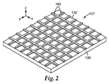
図2は、タッチスクリーンパネルの接触感知領域、例えば、図1の接触感知領域105内に位置する導電性可視光線透明区域101の斜視図を例示する。導電性可視光線透明区域101は、可視光線透明基材130、及び可視光線透明基材130の上又は中に配置される導電性微小パターン140を含む。可視光線透明基材130は、主表面132を含み、電気的に絶縁性である。可視光線透明基材130は、例えば、ガラス又はポリマーなどの任意の有用な電気的に絶縁性の材料から形成され得る。光線透明基材130の有用なポリマーの例としては、ポリエチレンテレフタレート(PET)、ポリカーボネート(PC)、ポリカーボネートコポリマー、及びポリエチレンナフタレート(PEN)が挙げられる。導電性微小パターン140は、複数の線形金属構造から形成され得る。
FIG. 2 illustrates a perspective view of a conductive visible light
図2はまた、タッチスクリーンパネルの接触感知領域内に位置する導電性可視光線透明区域101の説明に使用するための軸系を例示する。一般に、ディスプレイ装置の場合、x軸及びy軸はディスプレイの幅及び長さに相当し、z軸は典型的にディスプレイの厚さ(即ち、高さ)方向に沿っている。この取り決めは、特に明記しない限り、全体を通して使用される。図2の軸系において、x軸及びy軸は、可視光線透明基材130の主要面132と平行に画定され、正方形又は矩形表面の幅及び長さ方向に対応し得る。z軸は、この主表面と垂直であり、典型的には可視光線透明基材130の厚さ方向に沿っている。導電性微小パターン140を形成する複数の線形金属構造の幅は、y軸に沿って直線的に延びる平行の線形金属構造のx方向の間隔に相当し、直交する線形金属構造のy方向の間隔は、直交する線形金属構造の幅に相当する。線形金属構造の厚さ、即ち高さは、z方向の距離に相当する。
FIG. 2 also illustrates an axis system for use in describing the conductive visible light
図示されている実施形態では、タッチスクリーンパネルの接触感知領域内に位置する導電性可視光線透明区域101は、それぞれが導電性微小パターン140を有する、可視光線透明基材130の2つ以上の層を含む。
In the illustrated embodiment, the conductive visible light
導電性微小パターン140は、主表面132上に堆積される。センサは、タッチスクリーンディスプレイ、又はタッチパネルディスプレイを形成するために、ディスプレイと相互作用するため、基材130は、可視光線透明性であり、実質的に平面的である。基材及びセンサは、実質的に平面的、かつ可撓性であってよい。可視光線透明性とは、ディスプレイによってレンダリングされる情報(例えば、文字、画像、又は数字)が、タッチセンサを通して見えることを意味する。堆積された金属、更に光を遮蔽するために十分な厚さで堆積された金属の形態の導電体を含む、タッチセンサの視認性及び透明性は、金属が適切な微小パターンで堆積された場合に、達成され得る。
導電性微小パターン140は、情報をレンダリングするディスプレイの可視部分に重なる、少なくとも1つの可視光線透明導電性区域を含む。可視光線透明導電体とは、ディスプレイの一部分が、導電性微小パターンの区域を通して見ることができ、かつ微小パターンの区域が、パターンの平面において、又は換言すれば、導電性微小パターンが堆積され、これが隣接する基材の主表面に沿って導電性であることを意味する。
The
いくつかの実施形態において、本明細書に記載の物品は、可視光線透明基材の上又は中に配置された繰り返しセル形状の第1オープンメッシュを画定する線状トレースを含む第1導電性微小パターンと、その第1導電性微小パターンから電気的に絶縁された繰り返しセル形状の第2オープンメッシュを画定する線状トレースを含む第2導電性微小パターンとを含む。第2導電性微小パターンは、第1導電性微小パターンと同じ基材上に配置してもよく、又は別の基材上に配置してもよい。第2導電性微小パターンは、後述されるように、特定の配置で第1導電性微小パターン上に重ね合わせられる。 In some embodiments, an article described herein includes a first conductive micrometer comprising linear traces defining a first open mesh of a repetitive cell shape disposed on or in a visible light transparent substrate. A pattern and a second conductive micropattern including a linear trace defining a second open mesh of a repetitive cell shape that is electrically isolated from the first conductive micropattern. The second conductive micropattern may be disposed on the same substrate as the first conductive micropattern, or may be disposed on another substrate. As will be described later, the second conductive micropattern is superposed on the first conductive micropattern in a specific arrangement.
いくつかの実施形態において、両方の導電性微小パターンが、前述のように、タッチセンサ(例えばタッチスクリーンセンサ)の少なくとも一部を形成する。 In some embodiments, both conductive micropatterns form at least a portion of a touch sensor (eg, a touch screen sensor) as described above.
あるいは、他の実施形態では、導電性微小パターンの一方がタッチセンサ(例えばタッチスクリーンセンサ)の少なくとも一部を形成し、もう一方の導電性微小パターンがワイヤレス通信のアンテナとして機能してもよい。 Alternatively, in another embodiment, one of the conductive micropatterns may form at least a part of a touch sensor (eg, a touch screen sensor), and the other conductive micropattern may function as an antenna for wireless communication.
更に別の実施形態では、導電性微小パターンの一方がタッチセンサ(例えばタッチスクリーンセンサ)の少なくとも一部を形成し、もう一方の導電性微小パターンが電磁干渉(EMI)シールドとして機能してもよい。 In yet another embodiment, one of the conductive micropatterns may form at least a portion of a touch sensor (eg, a touch screen sensor) and the other conductive micropattern may function as an electromagnetic interference (EMI) shield. .
更に別の実施形態では、導電性微小パターンの一方がワイヤレス通信のアンテナの少なくとも一部を形成し、もう一方の導電性微小パターンが電磁干渉(EMI)シールドとして機能してもよい。 In yet another embodiment, one of the conductive micropatterns may form at least a portion of an antenna for wireless communication, and the other conductive micropattern may function as an electromagnetic interference (EMI) shield.
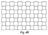
好ましい導電性微小パターンには、2次元メッシュ(又は単にメッシュ)を備えた区域があり、ここで、微小パターンラインなどの複数の線状微小パターン構造(しばしば導電体トレース又は金属トレースと呼ばれる)が、このメッシュ内に囲まれたオープン領域を画定する。この(例えば金属の)微小パターンによって画定されるオープン領域は、図3Bに示すような正方形形状セルなどのセル、及び図3Aに示すような六角形(即ち正六角形)形状セルとして記述することができる。 Preferred conductive micropatterns include areas with a two-dimensional mesh (or simply a mesh), where a plurality of linear micropattern structures such as micropattern lines (sometimes referred to as conductor traces or metal traces). Define an open region enclosed within the mesh. The open area defined by this (eg metallic) micropattern can be described as a cell such as a square shaped cell as shown in FIG. 3B and a hexagonal (ie regular hexagonal) shaped cell as shown in FIG. 3A. it can.
第1導電性微小パターン及び第2導電性微小パターンは一般に、繰り返しセル形状のオープンメッシュを画定する線状トレースを含む。繰り返しセル形状とは、その微小パターンが並進対称性を有することを意味する。図3A及び3Bは、セルが同じ寸法及び同じセル形状を有するようなセルの配列を有するセル設計を示しているが、導電性微小パターンは、2つ以上の異なるセル形状を含む繰り返しセル形状を有してもよい。例えば、図4A及び4Bは、繰り返しセグメントが正方形セルと八角形セルとの組み合わせを含む繰り返しセル形状のオープンメッシュを示す図である。典型的に、微小パターンは比較的短い距離で繰り返される。いくつかの実施形態において、この繰り返しセグメントは2つ又は3つ以下のセルを含む。図示されているオープンメッシュには境界線が直線の多角形セル形状のさまざまな配置が含まれるが、このセルは、繰り返しパターンを有する微小パターンを形成する限りにおいて、波状又は不規則な線状トレースで画定されてもよい。ゆえに、メッシュ又は導電性微小パターン全体の少なくとも一部分について少なくとも一方向に並進することができる繰り返しセグメント(又は基本単位(primitive))がある限りにおいて、異なる形状及び/又は異なる寸法を有する複数のセルを含む繰り返しセル形状は、本開示の範囲内である。 The first conductive micropattern and the second conductive micropattern generally include linear traces that define a repetitive cell-shaped open mesh. The repeated cell shape means that the minute pattern has translational symmetry. 3A and 3B show a cell design having an array of cells such that the cells have the same dimensions and the same cell shape, but the conductive micropattern has a repetitive cell shape that includes two or more different cell shapes. You may have. For example, FIGS. 4A and 4B are diagrams showing an open mesh having a repetitive cell shape in which a repetitive segment includes a combination of square cells and octagonal cells. Typically, the micropattern is repeated at a relatively short distance. In some embodiments, this repeating segment includes no more than two or three cells. The open mesh shown includes various arrangements of polygonal cell shapes with straight boundaries, but this cell can be a wavy or irregular linear trace as long as it forms a micropattern with a repeating pattern. May be defined. Thus, as long as there are repeating segments (or primitives) that can be translated in at least one direction for at least a portion of the entire mesh or conductive micropattern, cells having different shapes and / or different dimensions Including repeating cell shapes are within the scope of the present disclosure.
本明細書で使用されるとき、「セルの形状」とはその形を指し、寸法とは区別される。セル形状には、正方形、正方形ではない矩形、六角形、八角形、その他の多角形、又はその他の自由形状が挙げられる。正六角形は非正六角形とは異なる形状を有し、非正六角形は、少なくとも1つの縁部が別の縁部と長さが異なるか、又は少なくとも一夾角が120度に等しくない。2つのセルが同じ形状及び同じ寸法を有するとき、セルは互いに重ね合わせることができる。 As used herein, “cell shape” refers to its shape and is distinct from its dimensions. Cell shapes include squares, non-square rectangles, hexagons, octagons, other polygons, or other free shapes. A regular hexagon has a shape that is different from a non-regular hexagon, and the non-regular hexagon has at least one edge that is different in length from another edge, or at least one angle of depression not equal to 120 degrees. When two cells have the same shape and the same dimensions, the cells can overlap each other.
いくつかの実施形態において、第1微小パターン又は第2微小パターンのいずれかは、正のセル形状を有するセルのパターン(例えば繰り返しパターン)を含む。いくつかの実施形態において、第1微小パターン又は第2微小パターンの両方は、正のセルの形状を有するセルのパターン(例えば繰り返しパターン)を含む。いくつかの実施形態において、第1微小パターン又は第2微小パターンの両方は、同じ正のセル形状を有するセルを含む。「正のセル形状」とは、微小パターンのセルが正多角形の形状を有することを意味する。正多角形は、全ての縁部の長さが等しく、全ての夾角の角度が等しい。 In some embodiments, either the first micropattern or the second micropattern comprises a pattern of cells having a positive cell shape (eg, a repeating pattern). In some embodiments, both the first micropattern or the second micropattern includes a pattern of cells having a positive cell shape (eg, a repeating pattern). In some embodiments, both the first micropattern or the second micropattern include cells having the same positive cell shape. “Positive cell shape” means that a micropattern cell has a regular polygonal shape. A regular polygon has the same length at all edges and the same angle of depression.
いくつかの実施形態では、導電性微小パターンを画定する導電トレースは、5つの隣接するセル、好ましくは4つの隣接するセル、より好ましくは3つの隣接するセル、更により好ましくは2つの隣接するセルの合わせた縁部の長さよりも大きな距離にわたってほぼ直線的である区分を含まないように設計される。より好ましくは、微小パターンを画定するトレースは、単一のセルの縁部の長さよりも大きな距離にわたって直線的である区分を含まないように設計される。したがって、いくつかの実施形態では、微小パターンを画定するトレースは、長い距離、例えば、10センチメートル、1センチメートル、又は更に1ミリメートルを超えて直線的であることはない。直前に述べた、最小の長さの直線区分を有するパターンは、ディスプレイの視認性に最小限の障害しか生じさせない利点を有するタッチスクリーンセンサにとって特に有用である。 In some embodiments, the conductive traces that define the conductive micropattern comprise five adjacent cells, preferably four adjacent cells, more preferably three adjacent cells, and even more preferably two adjacent cells. It is designed not to include sections that are substantially linear over a distance greater than the combined edge length. More preferably, the traces defining the micropattern are designed not to include sections that are linear over a distance greater than the length of a single cell edge. Thus, in some embodiments, the traces that define the micropattern are not linear beyond a long distance, eg, 10 centimeters, 1 centimeter, or even 1 millimeter. The pattern just described with a minimal length of straight section is particularly useful for touch screen sensors that have the advantage of causing minimal disruption to display visibility.
いくつかの実施形態において、第1微小パターン及び第2微小パターンそれぞれは正方形メッシュを含む。他の実施形態では、微小パターンの一方は正方形メッシュを含み、もう一方の微小パターンは六角形(例えば正六角形)メッシュを含む。重ね合わせられた好ましい導電性微小パターンは、2次元の連続的なメッシュ(例えば金属メッシュ)を備えた第1微小パターン区域及び第2微小パターン区域を含み、ここにおいてメッシュを形成する線状トレースの少なくとも一部分は非平行であり、例えば三角形(例えば正三角形)、五角形、及び六角形(例えば正六角形)のネットワークなど、特定の多角形ネットワークである。より好ましくは、第1微小パターン及び第2微小パターンはそれぞれ、多角形(例えば正多角形)のメッシュを含む。 In some embodiments, each of the first micropattern and the second micropattern includes a square mesh. In other embodiments, one of the micropatterns includes a square mesh and the other micropattern includes a hexagonal (eg, regular hexagonal) mesh. The preferred superposed conductive micropattern includes a first micropattern area and a second micropattern area with a two-dimensional continuous mesh (eg, a metal mesh), in which the linear traces forming the mesh At least a portion is non-parallel and is a particular polygonal network, such as a network of triangles (eg, regular triangles), pentagons, and hexagons (eg, regular hexagons). More preferably, each of the first micro pattern and the second micro pattern includes a polygonal mesh (for example, a regular polygon).
導電性微小パターンの2次元形状(即ち、平面内、又は基材の主表面に沿ったパターンの形状)は、タッチスクリーンセンサにおいて有用な特別な透明導電特性を達成するために、導電体材料の光学的及び電気的特性を考慮して設計され得る。 The two-dimensional shape of the conductive micropattern (ie, the shape of the pattern in the plane or along the major surface of the substrate) is used to achieve special transparent conductive properties useful in touch screen sensors. It can be designed in consideration of optical and electrical properties.
センサの透明性、及びセンサを通したディスプレイの視認性を達成するための導電体の適切な微小パターンは、一定の特質を有する。まず、これを通してディスプレイが見られる導電性微小パターンの区域は、50%未満、又は25%未満、又は20%未満、又は10%未満、又は5%未満、又は4%未満、又は3%未満、又は2%未満、又は1%未満、又は0.25%〜0.75%の範囲、又は0.5%未満の、導電体によって遮蔽されるセンサの面積率を有するべきである。 Appropriate micropatterns of electrical conductors to achieve sensor transparency and display visibility through the sensor have certain attributes. First, the area of the conductive micropattern through which the display is viewed is less than 50%, or less than 25%, or less than 20%, or less than 10%, or less than 5%, or less than 4%, or less than 3%, Or should have a sensor area ratio shielded by electrical conductors of less than 2%, or less than 1%, or in the range of 0.25% to 0.75%, or less than 0.5%.
導電性微小パターン、又は導電性微小パターンの区域の開放面積率(又は開放面積若しくは開放面積の比率)は、導電体によって遮蔽されていない微小パターン面積、又は区域面積の割合である。開放面積は、1から、導電体によって遮蔽される面積率を引いたものに相当し、少数又は百分率として、便利に及び互換的に表現することができる。導電体によって遮蔽される面積率は、微小パターン化された導電体の線の密度と互換的に使用される。微小パターン化された導電体は、電気的に導電性の微小パターン及び導電性微小パターンと互換的に使用される。したがって、導電体によって遮蔽される割合に関して上の文章で示された値に関し、開放面積値は、50%超、75%超、80%超、90%超、95%超、96%超、97%超、98%超、99%超、99.25〜99.75%、99.8%、99.85%、99.9%、及び更に99.95%である。いくつかの実施形態では、導電性微小パターンの区域の開放面積(例えば、可視光線透明導電性区域)は、80%〜99.5%であり、他の実施形態では90%〜99.5%であり、他の実施形態では、95%〜99%であり、他の実施形態では、96%〜99.5%であり、他の実施形態では、97%〜98%であり、他の実施形態では、最大99.95%である。実際的な製造方法を使用した、有用な光学的特性(例えば、導電パターン要素の高い透過率及び無視認性)、及び電気的特性の再現可能な達成に関し、開放面積の好ましい値は、90〜99.5%、より好ましくは95〜99.5%であり、いくつかの実施形態では95〜99.95%である。 The open area ratio (or the open area or the ratio of the open area) of the conductive micropattern or the area of the conductive micropattern is a ratio of the micropattern area or the area of the area that is not shielded by the conductor. The open area corresponds to 1 minus the area ratio shielded by the conductor and can be conveniently and interchangeably expressed as a minority or percentage. The area ratio shielded by the conductor is used interchangeably with the density of the micropatterned conductor lines. Micropatterned conductors are used interchangeably with electrically conductive micropatterns and conductive micropatterns. Thus, for the values given in the above text for the percentage shielded by the conductor, the open area values are over 50%, over 75%, over 80%, over 90%, over 95%, over 96%, 97 %, 98%, 99%, 99.25 to 99.75%, 99.8%, 99.85%, 99.9%, and even 99.95%. In some embodiments, the open area of the area of the conductive micropattern (eg, visible light transparent conductive area) is 80% to 99.5%, and in other embodiments 90% to 99.5%. In other embodiments, from 95% to 99%, in other embodiments from 96% to 99.5%, in other embodiments, from 97% to 98%, In form, the maximum is 99.95%. With respect to useful optical properties (eg, high transmission and invisibility of conductive pattern elements) using practical manufacturing methods, and reproducible achievement of electrical properties, preferred values of open area are from 90 to 99.5%, more preferably 95-99.5%, and in some embodiments 95-99.99%.
干渉(例えば一部ディスプレイのピクセルパターンとの干渉)を最少化し、ユーザー又は見る人の裸眼によるパターン要素(例えば、導電体の線)の視認性を回避するために、導電パターン要素の最小寸法(例えば、線又は導電トレースの幅)は、およそ50マイクロメートル以下、又はおよそ25マイクロメートル以下、又はおよそ10マイクロメートル以下、又はおよそ5マイクロメートル以下、又はおよそ4マイクロメートル以下、又はおよそ3マイクロメートル以下、又はおよそ2マイクロメートル以下、又はおよそ1マイクロメートル以下、又はおよそ0.5マイクメートル以下であるべきである。1つ以上の重ね合わせられた導電性微小パターンの設計においては、その1つ以上の重ね合わせられた導電性微小パターンとディスプレイピクセルとの間のモアレ効果などの干渉を最小限に抑えるために、当該技術分野において既知の概念を含めることができる。 In order to minimize interference (e.g. interference with the pixel pattern of some displays) and avoid the visibility of pattern elements (e.g. conductor lines) by the naked eye of the user or viewer, For example, the width of the line or conductive trace) is approximately 50 micrometers or less, or approximately 25 micrometers or less, or approximately 10 micrometers or less, or approximately 5 micrometers or less, or approximately 4 micrometers or less, or approximately 3 micrometers. Should be less than or about 2 micrometers or less, or about 1 micrometer or less, or about 0.5 micrometer or less. In designing one or more superimposed conductive micropatterns, in order to minimize interference such as moire effects between the one or more superimposed conductive micropatterns and display pixels, Concepts known in the art can be included.
いくつかの実施形態では、導電パターン要素の最小寸法は、0.5〜50マイクロメートル、他の実施形態では、0.5〜25マイクロメートル、他の実施形態では、1〜10マイクロメートル、他の実施形態では、1〜5マイクロメートル、他の実施形態では、1〜4マイクロメートル、他の実施形態では、1〜3マイクロメートル、他の実施形態では、0.5〜3マイクロメートル、及び他の実施形態では、0.5〜2マイクロメートルである。有用な光学的特性(例えば、裸眼による導電パターン要素の高い透過率及び無視認性)、及び電気的特性の再現可能な達成に関し、実際的な製造方法の使用による制約を考慮し、導電パターン要素の最小寸法の好ましい値は、0.5〜5マイクロメートル、より好ましくは1〜4マイクロメートルであり、最も好ましくは1〜3マイクロメートルである。 In some embodiments, the minimum dimension of the conductive pattern element is 0.5-50 micrometers, in other embodiments 0.5-25 micrometers, in other embodiments 1-10 micrometers, etc. 1 to 5 micrometers in other embodiments, 1 to 4 micrometers in other embodiments, 1 to 3 micrometers in other embodiments, 0.5 to 3 micrometers in other embodiments, and In other embodiments, 0.5 to 2 micrometers. Concerning useful optical properties (for example, high transmittance and invisibility of conductive pattern elements by the naked eye) and reproducible achievement of electrical properties, considering the limitations of using practical manufacturing methods, conductive pattern elements The preferred value of the minimum dimension is 0.5 to 5 micrometers, more preferably 1 to 4 micrometers, and most preferably 1 to 3 micrometers.
重ね合わせられた微小パターンの特定の配置が、微小パターンの組み合わせについて低視認性をもたらし、一方で他の配置では、微小パターンの組み合わせについて高視認性をもたらすことが見出されている。 It has been found that certain arrangements of superimposed micropatterns provide low visibility for micropattern combinations, while other arrangements provide high visibility for micropattern combinations.
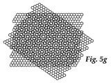
図5a〜5cは、2層の同じ正六角形メッシュ重ね合わせを示す図である。第2微小パターンが第1微小パターンに対して回転しており、図5aの5度から始まって、図5aから5cへと5度刻みでそれぞれ増加した角度になっている。図5aにおいて、見かけの複合パターンが存在し、各複合パターンの中央は、少なくとも約4つのセル分の直径を有している。したがって、この見かけの複合パターンは、導電性構造の寸法、又はいずれかの微小パターンの導電性構造間の間隔よりも大きい空間寸法を有する。更に、見かけの複合パターンは、典型的に、繰り返し形状の繰り返しセグメントよりも大きい空間寸法を有する。図5b及び5cでは、見かけの複合パターンの大きさはより小さく、中央部分はそれぞれセル約3つ分及び2つ分の直径にわたっている。図示目的のため、図5a〜5iのメッシュの個々の線状トレースは明白であり識別可能にしている。六角形セルも、明白であり識別可能である。しかしながら、パターンが微小パターンである場合、個々の線状トレースは識別不能であり、個々のセルも識別できない。しかし、微小パターンの重ね合わせによって生じた複合パターンはきわめて視認性(明白)であるが、必ずしも識別可能ではない。 5a-5c are diagrams showing two layers of the same regular hexagon mesh overlay. The second micropattern is rotating relative to the first micropattern, starting at 5 degrees in FIG. 5a and increasing in increments of 5 degrees from FIGS. 5a to 5c. In FIG. 5a, there is an apparent composite pattern, and the center of each composite pattern has a diameter of at least about 4 cells. Thus, this apparent composite pattern has a spatial dimension that is larger than the dimensions of the conductive structures or the spacing between the conductive structures of any micropattern. Furthermore, the apparent composite pattern typically has a larger spatial dimension than a repeating segment of a repeating shape. In FIGS. 5b and 5c, the apparent composite pattern is smaller in size, with the central portion spanning about three and two cell diameters, respectively. For illustration purposes, the individual linear traces of the mesh of FIGS. 5a-5i are clear and distinguishable. Hexagonal cells are also obvious and distinguishable. However, when the pattern is a minute pattern, individual linear traces cannot be identified, and individual cells cannot be identified. However, the composite pattern generated by superimposing the micropatterns is very visible (obvious), but is not always identifiable.
重ね合わせられた導電性メッシュ微小パターン(例えば繰り返しセル形状を伴う)の特定の設計及び配置は、特に特定の設計を使用した場合、一定間隔で画素化されたディスプレイと組み合わせたときに低視認性を有し得る。この視認性は、ランダム又は擬似ランダムなセル形状を有する一部の導電性メッシュ微小パターンよりも更に低くなり得ることが推測される。重要なこととして、設計及び配置は、2つの導電性微小パターンを重ね合わせたときの視認性低下に関連する。 Specific design and placement of superimposed conductive mesh micropatterns (eg with repetitive cell shapes), especially when using specific designs, low visibility when combined with regularly spaced pixelated displays Can have. It is speculated that this visibility can be even lower than some conductive mesh micropatterns having random or pseudo-random cell shapes. Importantly, design and placement are related to reduced visibility when two conductive micropatterns are superimposed.
低視認性を得る一実施形態において、第2導電性微小パターンは、第2導電性微小パターンの線状トレースの少なくとも一部分が、第1導電性微小パターンの線状トレースに対して非平行であるように、第1導電性微小パターンに重ね合わせられる。 In one embodiment for obtaining low visibility, the second conductive micropattern is such that at least a portion of the linear trace of the second conductive micropattern is non-parallel to the linear trace of the first conductive micropattern. As described above, the first conductive micropattern is overlaid.
第1導電性微小パターン及び第2導電性微小パターンを特定の相対的向きに意図的に配置することは、本開示の範囲内である。特定の相対的向きで配置された2つの導電性微小パターンは、互いに対してある既定の角度(又は既定のバイアス角)を有し得る。第2導電性微小パターンに対する1つの導電性微小パターンの角度は、これら2つの微小パターンが、同じセル形状を有する繰り返しセグメントを含む場合に、容易に明らかである。いくつかの実施形態について、バイアス角を定義するための手順を以下に述べる。2つの微小パターンが、同じセル形状を有する繰り返しセグメントを含む場合、この2つの微小パターンについて、これら微小パターンが共有する単一微小パターン形状の回転対称性に基づき、同等の方向の同じ組を定義することができる。例えば、六角形メッシュの場合は、メッシュ形状の6面回転対称性に関連して、6つの同等方向を選択することができる。別の例として、正方形メッシュの場合は、メッシュ形状の4面回転対称性に関連して、4つの同等方向を選択することができる。2つのメッシュについて同様に定義されるそのような同等方向により、2つの導電性微小パターン間の角度(即ちバイアス角度又は相対的向き)を画定又は測定するための基準が得られる。2つの導電性微小パターン間の角度は、第1導電性微小パターンの同等方向と第2導電性微小パターンの同等方向とを分離している最小角度である。2つの導電性微小パターンが同じ繰り返しセグメントセル形状を有するメッシュ微小パターンであるような場合においては、依然として、微小パターンの組み合わせの外観が、バイアス角度の変化に関して周期的となる。バイアス角度増加に伴う外観変化の角周期は、360度を回転対称性レベルで割ったものに等しくなる(例えば、回転対称性がない場合は1、2面回転対称性の場合は2、3面回転対称性の場合は3、4面回転対称性の場合は4、及び6面回転対称性の場合は6)。用語「繰り返し角度」は、本明細書において角度周期を記述するのに使用される。よって、同じセル形状を含む2つの導電性微小パターンの組み合わせについて、固有の(外観に関して)組み合わせられた形状は、0度〜[360/回転対称性レベル]の角度の範囲のみに存在する。重ね合わせられた微小パターンの組み合わせられた形状は、バイアス角度に関して周期的(前述のように、繰り返し角度で)であるが、組み合わせられた微小パターンの全体的な外観に関しては、繰り返し角度の1/2でバイアス角度を規定することが同様に有用である場合がある。これは、全体的な外観が、バイアス角度xと、[繰り返し角度−x]のバイアス角度とで同じであり得るためである(ここでxは繰り返し角度の1/2より小さい)。よって、組み合わせられた微小パターンの外観の全範囲は、0度から繰り返し角度の1/2までのバイアス角度範囲内で画定され得る。場合によっては、同じメッシュ形状を含む導電性微小パターン間のバイアス角度を、繰り返し角度の分数として画定することが有用である。いくつかの実施形態において、バイアス角度は繰り返し角度の0.1〜0.9倍である。好ましい実施形態では、バイアス角度は繰り返し角度の0.1〜0.4倍、又は0.6〜0.9倍である。別の好ましい実施形態では、バイアス角度は繰り返し角度の0.2〜0.3倍、又は0.7〜0.8倍である。 It is within the scope of this disclosure to intentionally place the first conductive micropattern and the second conductive micropattern in a specific relative orientation. Two conductive micropatterns arranged in a particular relative orientation may have a certain predetermined angle (or a predetermined bias angle) relative to each other. The angle of one conductive micropattern with respect to the second conductive micropattern is readily apparent when these two micropatterns contain repeating segments having the same cell shape. The procedure for defining the bias angle for some embodiments is described below. When two micropatterns contain repeated segments having the same cell shape, the same set of equivalent directions is defined for the two micropatterns based on the rotational symmetry of the single micropattern shape shared by these micropatterns. can do. For example, in the case of a hexagonal mesh, six equivalent directions can be selected in connection with the six-plane rotational symmetry of the mesh shape. As another example, in the case of a square mesh, four equivalent directions can be selected in relation to the four-plane rotational symmetry of the mesh shape. Such equivalent directions, defined similarly for the two meshes, provide a reference for defining or measuring the angle (ie, bias angle or relative orientation) between the two conductive micropatterns. The angle between the two conductive micropatterns is the minimum angle separating the equivalent direction of the first conductive micropattern and the equivalent direction of the second conductive micropattern. In the case where the two conductive micropatterns are mesh micropatterns having the same repetitive segment cell shape, the appearance of the micropattern combination is still periodic with respect to changes in the bias angle. The angular period of the appearance change with increasing bias angle is equal to 360 degrees divided by the rotational symmetry level (for example, in the case of no rotational symmetry, 2 or 3 in the case of 1-plane rotational symmetry) 3 for rotational symmetry, 4 for rotational symmetry, 4 for rotational symmetry, and 6 for 6 rotational symmetry. The term “repeat angle” is used herein to describe an angular period. Thus, for a combination of two conductive micropatterns that contain the same cell shape, the unique (in terms of appearance) combined shape exists only in the range of angles from 0 degrees to [360 / rotation symmetry level]. The combined shape of the superimposed micropatterns is periodic (with a repeat angle as described above) with respect to the bias angle, but with respect to the overall appearance of the combined micropattern, it is 1 / of the repeat angle. It may be useful to define the bias angle at 2 as well. This is because the overall appearance can be the same for the bias angle x and the bias angle of [repetition angle-x] (where x is less than half of the repetition angle). Thus, the full range of appearance of the combined micropattern can be defined within a bias angle range from 0 degrees to half the repeat angle. In some cases, it is useful to define the bias angle between conductive micropatterns containing the same mesh shape as a fraction of the repeat angle. In some embodiments, the bias angle is 0.1 to 0.9 times the repeat angle. In a preferred embodiment, the bias angle is 0.1 to 0.4 times, or 0.6 to 0.9 times the repeat angle. In another preferred embodiment, the bias angle is 0.2 to 0.3 times, or 0.7 to 0.8 times the repeat angle.
図5a〜5iを参照すると、一実施形態において、第1微小パターンに対して第2微小パターンを回転させることにより、第2導電性微小パターンは、第1導電性微小パターンの線状トレースに対して非平行な線状トレースを有する。第1導電性微小パターンの形状は、第2導電性微小パターンの形状と同じである。両方の微小パターンの形状は、6面回転対称性を有する六角形メッシュである。繰り返し角度は60度である。第1微小パターン及び第2微小パターンが同じセル(例えば正則的)形状及び同じセル寸法を有する場合、相対的バイアス角度の使用は特に有用である。また、2つの微小パターンが異なる寸法のセルを有する場合、正のセル形状を含む第2導電性微小パターンに対して、同じ正のセル形状を含む1つの導電性微小パターンを回転させることも、非常に有用である。回転角度(バイアス角度)が、図5aに示す約5度(繰り返し角度の0.083倍)から、図5cに示す約15度(繰り返し角度の0.25倍)まで増加すると、視認性は減少し得る。回転角度は具体的なセル形状及びセル寸法によって異なり得るが、回転角度は好ましくは少なくとも10度(図5iに図示)かつ45度(図5iに図示)未満である。 Referring to FIGS. 5a-5i, in one embodiment, by rotating the second micropattern with respect to the first micropattern, the second conductive micropattern is relative to the linear trace of the first conductive micropattern. And non-parallel linear traces. The shape of the first conductive micropattern is the same as the shape of the second conductive micropattern. The shape of both micropatterns is a hexagonal mesh having 6-plane rotational symmetry. The repetition angle is 60 degrees. The use of relative bias angles is particularly useful when the first micropattern and the second micropattern have the same cell (eg, regular) shape and the same cell dimensions. In addition, when two micropatterns have cells of different dimensions, it is also possible to rotate one conductive micropattern including the same positive cell shape with respect to the second conductive micropattern including the positive cell shape. Very useful. Visibility decreases when the rotation angle (bias angle) increases from about 5 degrees (0.083 times the repeat angle) shown in FIG. 5a to about 15 degrees (0.25 times the repeat angle) shown in FIG. 5c. Can do. While the rotation angle may vary depending on the specific cell shape and cell dimensions, the rotation angle is preferably at least 10 degrees (shown in FIG. 5i) and less than 45 degrees (shown in FIG. 5i).
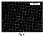
他の実施形態において、第2導電性微小パターンが、第1導電性微小パターンのセル形状とは異なるセル形状を有している結果として、第2導電性微小パターンは、第1導電性微小パターンの線状トレースに対して非平行である線状トレースを有する。例えば、図6を参照すると、第1導電性微小パターンが正方形セル形状、第2導電性微小パターンが六角形セル形状を有してよく、逆もまた同様である。正方形セルの線状トレースの一部分は六角形セルの線状トレースに対して平行であり得るが、線状トレースの一部分は非平行である。 In another embodiment, as a result of the second conductive micropattern having a cell shape that is different from the cell shape of the first conductive micropattern, the second conductive micropattern is the first conductive micropattern. The linear traces are non-parallel to the linear traces. For example, referring to FIG. 6, the first conductive micropattern may have a square cell shape and the second conductive micropattern may have a hexagonal cell shape, and vice versa. A portion of the square cell linear trace may be parallel to the hexagonal cell linear trace, but a portion of the linear trace is non-parallel.
低視認性を得るための他の一実施形態において、第2導電性微小パターンは、第1導電性微小パターンのセル寸法とは異なるセル寸法を有する。用語「セル寸法」とは一般に、メッシュ導電性微小パターンのセルのサイズを指す。正多角形の形状を有するセルの場合、(2つの導電性微小パターンのセル寸法を比較する目的で)セル寸法をセルの幅、例えば正方形セルの縁部長さとして、又は更なる一例として、多角形セルの平行面間の距離(本明細書では多角形の直径又はピッチとも呼ばれる)として定義するのが便利である。 In another embodiment for obtaining low visibility, the second conductive micropattern has a cell size different from the cell size of the first conductive micropattern. The term “cell dimension” generally refers to the size of the cells of the mesh conductive micropattern. In the case of a cell having a regular polygon shape, the cell dimension is used as the cell width, eg the edge length of a square cell, or as a further example (for the purpose of comparing the cell dimensions of two conductive micropatterns) Conveniently defined as the distance between parallel faces of square cells (also referred to herein as polygon diameter or pitch).
いくつかの実施形態において、導電性トレースから形成された正のセルの平均幅又はピッチは、典型的に500マイクロメートル以下、450マイクロメートル以下、又は400マイクロメートル以下である。いくつかの好ましい実施形態において、微小パターンは両方とも、350マイクロメートル以下、300マイクロメートル以下、250マイクロメートル以下、200マイクロメートル以下、150マイクロメートル以下、100マイクロメートル以下、又は50マイクロメートル以下の平均セル幅を有する。 In some embodiments, the average width or pitch of positive cells formed from conductive traces is typically 500 micrometers or less, 450 micrometers or less, or 400 micrometers or less. In some preferred embodiments, both micropatterns are 350 micrometers or less, 300 micrometers or less, 250 micrometers or less, 200 micrometers or less, 150 micrometers or less, 100 micrometers or less, or 50 micrometers or less. It has an average cell width.
正ではないセル形状については(又は正のセル形状についても)、繰り返しセル形状を有する2つのメッシュ導電性微小パターンのセル寸法を比較する目的のために、セル寸法は、セル形状の重心を通りセル形状の境界線の各方向に延在するすべての線分(即ちすべての向き)の平均長さとして定義することができる。 For non-positive cell shapes (or even for positive cell shapes), for the purpose of comparing the cell dimensions of two mesh conductive micropatterns with repeated cell shapes, the cell dimensions pass through the center of gravity of the cell shape. It can be defined as the average length of all line segments (ie, all orientations) extending in each direction of the cell-shaped boundary line.
同じ繰り返しセル形状を有する2つのメッシュ導電性微小パターンは、異なるセル寸法を有し得る。また、異なる繰り返しセル形状を有する2つのメッシュ導電性微小パターンは、異なるセル寸法を有し得る。いくつかの実施形態において、第1導電性微小パターンのセル寸法は、第2導電性微小パターンのセル寸法の1.1〜6倍に等しい(即ち、それぞれ1:1.1〜1:6の比)。第1導電性微小パターンのセル寸法は、第2導電性微小パターンのセル寸法の1.2〜3倍に等しいことが好ましく、より好ましくは1.2〜2倍である。 Two mesh conductive micropatterns having the same repeating cell shape may have different cell dimensions. Also, two mesh conductive micropatterns having different repetitive cell shapes can have different cell dimensions. In some embodiments, the cell size of the first conductive micropattern is equal to 1.1-6 times the cell size of the second conductive micropattern (ie, 1: 1.1 to 1: 6, respectively). ratio). The cell size of the first conductive micropattern is preferably equal to 1.2 to 3 times the cell size of the second conductive micropattern, and more preferably 1.2 to 2 times.
いくつかの好ましい実施形態において、第1導電性微小パターン及び第2導電性微小パターンは同じ繰り返しセル形状を有し、ここにおいて第1導電性微小パターンのセル寸法は第2導電性微小パターンのセル寸法の1.1〜6倍であり、これらパターン間のバイアス角度は、繰り返し角度の0.1〜0.9倍である。いくつかの実施形態において、これらパターン間のバイアス角度は、繰り返し角度の0.1〜0.4倍又は0.6〜0.9倍である。これら実施形態のいくつかにおいて、繰り返しセル形状には正多角形が含まれる。これら実施形態のいくつかにおいて、繰り返しセル形状は単一の正多角形から成る。これら実施形態のいくつかにおいて、繰り返しセル形状は正六角形から成る。 In some preferred embodiments, the first conductive micropattern and the second conductive micropattern have the same repetitive cell shape, wherein the cell size of the first conductive micropattern is the cell of the second conductive micropattern. The dimension is 1.1 to 6 times, and the bias angle between these patterns is 0.1 to 0.9 times the repeat angle. In some embodiments, the bias angle between these patterns is 0.1 to 0.4 times or 0.6 to 0.9 times the repeat angle. In some of these embodiments, the repeating cell shape includes a regular polygon. In some of these embodiments, the repeating cell shape consists of a single regular polygon. In some of these embodiments, the repeating cell shape consists of a regular hexagon.
いくつかの好ましい実施形態において、第1導電性微小パターン及び第2導電性微小パターンは同じ繰り返しセル形状を有し、ここにおいて第1導電性微小パターンのセル寸法は第2導電性微小パターンのセル寸法の1.2〜3倍であり、これらパターン間のバイアス角度は、繰り返し角度の0.6〜0.9倍である。これら実施形態のいくつかにおいて、繰り返しセル形状には正多角形が含まれる。これら実施形態のいくつかにおいて、繰り返しセル形状は単一の正多角形から成る。これら実施形態のいくつかにおいて、繰り返しセル形状は正六角形から成る。 In some preferred embodiments, the first conductive micropattern and the second conductive micropattern have the same repetitive cell shape, wherein the cell size of the first conductive micropattern is the cell of the second conductive micropattern. The size is 1.2 to 3 times, and the bias angle between these patterns is 0.6 to 0.9 times the repetition angle. In some of these embodiments, the repeating cell shape includes a regular polygon. In some of these embodiments, the repeating cell shape consists of a single regular polygon. In some of these embodiments, the repeating cell shape consists of a regular hexagon.
いくつかの好ましい実施形態において、第1導電性微小パターン及び第2導電性微小パターンは同じ繰り返しセル形状を有し、ここにおいて第1導電性微小パターンのセル寸法は第2導電性微小パターンのセル寸法の1.1〜6倍であり、これらパターン間のバイアス角度は、約10度〜約45度である。いくつかの実施形態において、第1導電性微小パターンのセル寸法は、第2導電性微小パターンのセル寸法の1.2〜3倍である。これら実施形態のいくつかにおいて、繰り返しセル形状には正多角形が含まれる。これら実施形態のいくつかにおいて、繰り返しセル形状は単一の正多角形から成る。これら実施形態のいくつかにおいて、繰り返しセル形状は正六角形から成る。 In some preferred embodiments, the first conductive micropattern and the second conductive micropattern have the same repetitive cell shape, wherein the cell size of the first conductive micropattern is the cell of the second conductive micropattern. 1.1-6 times the size, and the bias angle between these patterns is about 10 degrees to about 45 degrees. In some embodiments, the cell size of the first conductive micropattern is 1.2 to 3 times the cell size of the second conductive micropattern. In some of these embodiments, the repeating cell shape includes a regular polygon. In some of these embodiments, the repeating cell shape consists of a single regular polygon. In some of these embodiments, the repeating cell shape consists of a regular hexagon.
重ね合わせられた微小パターンの視認性は、さまざまな方法を使用して測定することができる。いくつかの実施形態において、重ね合わせられた微小パターンの視認性は、テストパネル(即ちヒト)の使用によって視認性を評価することによって測定される(実施例に記述される方法による)。 The visibility of the superimposed micropattern can be measured using various methods. In some embodiments, the visibility of the superimposed micropattern is measured by evaluating the visibility by use of a test panel (ie, human) (according to the method described in the examples).
「A Standard Model for Foveal Detection of Spatial Contrast」(Journal of Vision,2005 5,717〜740)に記述されている数学的モデルを使用して、ヒトの裸眼正常視力(即ち20/20)で、画像が明白であり(即ち容易に見ることができ、可視である)、識別可能である(即ち最終的な特性を確認するために)ような、十分な寸法を有する画像の視認性が評価されているが、そのような数学的モデルは、明白でない微小パターン又は重ね合わせられた微小パターンの視認性を測定するための使用に適合されているとは考えられない。 Using the mathematical model described in “A Standard Model for Focal Detection of Spatial Contrast” (Journal of Vision, 2005, 717-740), images with normal human eyesight (ie 20/20) The visibility of an image with sufficient dimensions such that it is obvious (i.e. easily visible and visible) and identifiable (i.e. to confirm final properties) However, such a mathematical model is not considered adapted for use to measure the visibility of unclear or overlaid micropatterns.
したがって、他の実施形態において、微小パターン基材(例えば重ね合わせられた微小パターン)のデジタル画像を提供することと、そのデジタル画像の空間コントラスト閾値を、窩検出モデル(即ち標準空間観測者モデル)で計算することとを含む、パターン基材の視認性を測定する方法が記述されている。 Thus, in other embodiments, providing a digital image of a micropatterned substrate (eg, a superposed micropattern) and the spatial contrast threshold of the digital image is determined by a foveal detection model (ie, a standard spatial observer model). A method for measuring the visibility of a patterned substrate is described.
数学的モデルは、さまざまな理由から、テストパネル(即ちヒト)よりも好ましい可能性がある。テストパネルは通常、より主観的であり、一般に、統計学的に有意な結果を得るため複数の参加者を必要とする。更に、テストパネルの使用は通常、視認性を評価することができるためには、実際のサンプルが微小パターンそれぞれから作られる必要がある。 The mathematical model may be preferred over the test panel (ie human) for a variety of reasons. Test panels are usually more subjective and generally require multiple participants to obtain statistically significant results. Furthermore, the use of a test panel usually requires that an actual sample be made from each micropattern in order to be able to assess visibility.
数学的モデルのインプットも、(例えば光学的透明)基材及び非透明の微小パターンを含むサンプルを供給することによって生成することができ、これにより、使用中にサンプルが観測されるときのサンプルの光条件をシミュレーションし、デジタル的にサンプルを画像化する。しかしながら、数学的モデルも、デジタル的に設計された微小パターンのデジタル画像を利用することができる。ゆえに、この実施形態においては、微小パターン又は重ね合わせられた微小パターンの視認性を、実際に物理的サンプルを製造することなく評価することができる。これは、実際の製造なしに複数の微小パターンの視認性をより効率的に評価するのに適している。 A mathematical model input can also be generated by supplying a sample containing a substrate (eg optically transparent) and a non-transparent micropattern, which allows the sample to be observed as it is observed during use. Simulate light conditions and digitally image the sample. However, mathematical models can also use digital images of minute patterns designed digitally. Therefore, in this embodiment, the visibility of the minute pattern or the superimposed minute pattern can be evaluated without actually manufacturing a physical sample. This is suitable for more efficiently evaluating the visibility of a plurality of minute patterns without actual manufacturing.
テストパネル(即ちヒト)又は数学モデルのいずれを使用するかにかかわらず、微小パターン基材のデジタル画像、又はそのデジタル設計は、通常、微小パターンのみを含めるようトリミングされる。重ね合わせられたパターン内に実際に存在しない、トリミングの結果生じた縁部又は境界は、コントラスト閾値を計算する前に除外すべきである。透過中(即ち、基材を通して透過するバックライトで微小パターンを見ているとき)、金属微小パターンは、透明背景に対して暗色に見えるが、反射光で見たときの微小パターンの外観をシミュレーションするためには、デジタル的に改変して(例えばコンピュータ画面上で画像の極性を反転させることにより)、透明基材を暗色に、微小パターンを明色になるようにすることが好ましい。このように微小パターンのデジタル的改変をしないモデルによって、異なるコントラスト閾値を計算することができる。 Regardless of whether a test panel (ie, human) or mathematical model is used, the digital image of the micropattern substrate, or its digital design, is usually cropped to include only the micropattern. Edges or boundaries resulting from trimming that are not actually present in the overlaid pattern should be excluded before calculating the contrast threshold. During transmission (ie, when viewing a micropattern with a backlight that is transmitted through the substrate), the metal micropattern appears dark against a transparent background, but simulates the appearance of the micropattern when viewed with reflected light In order to achieve this, it is preferable to digitally modify the image (for example, by inverting the polarity of the image on the computer screen) so that the transparent substrate is dark and the minute pattern is light. In this way, different contrast thresholds can be calculated by a model that does not digitally modify a micropattern.
本明細書で記述されている計算したコントラスト閾値(実施例に記述されているように実施)は、テストパネル(即ちヒト)によって測定された視認性に対応していることが見出されている。微小パターン又は重ね合わせられた微小パターンが−35デシベル未満のコントラスト閾値を有する場合、この微小パターンは最も視認性である。したがって、コントラスト閾値は−35デシベルより大きいことが好ましい。コントラスト閾値が−30デシベル又は−25デシベルより大きいとき、微小パターン(例えば重ね合わせられた微小パターンのビートパターン)はまだ明白であり、識別可能である。しかしながら、微小パターン又は重ね合わせられた微小パターンが−24、−23、−22、−21、又は−20デシベルより大きい予想コントラスト閾値を有する場合、この微小パターン又は重ね合わせられた微小パターンは実質的に、視認性が低くなる。好ましい実施形態において、コントラスト閾値は−15デシベル、−10デシベル、又は−5デシベルよりも大きい。微小パターン又は重ね合わせられた微小パターンが0以上の予想コントラスト閾値を有する場合、その微小パターン又は重ね合わせられた微小パターンは目に見えない。コントラスト閾値が増加すると、サンプル外観の均一性が増大する。 The calculated contrast threshold described herein (performed as described in the examples) has been found to correspond to the visibility measured by the test panel (ie, human). . If the micropattern or the superimposed micropattern has a contrast threshold less than -35 dB, this micropattern is most visible. Therefore, the contrast threshold is preferably greater than -35 dB. When the contrast threshold is greater than −30 decibels or −25 decibels, the micropattern (eg, the beat pattern of the superimposed micropattern) is still obvious and can be distinguished. However, if the micropattern or the superimposed micropattern has an expected contrast threshold greater than −24, −23, −22, −21, or −20 decibels, the micropattern or the superimposed micropattern is substantially In addition, the visibility is lowered. In preferred embodiments, the contrast threshold is greater than −15 dB, −10 dB, or −5 dB. When the micropattern or the superimposed micropattern has an expected contrast threshold value of 0 or more, the micropattern or the superimposed micropattern is not visible. As the contrast threshold increases, the uniformity of the sample appearance increases.
コントラスト閾値の差における1デシベルの違いは、平均的なヒトの観測者にとって「ようやく気づく違い」である。 The difference of 1 dB in the difference in contrast threshold is a “difference finally noticed” for the average human observer.
コントラスト閾値を計算するための距離は変動し得るが、関心対象の観測距離(即ち、通常は、普通の使用中における微小パターン基材の平均的観測距離)に合わせて選択される。例えば、物品が携帯電話のタッチセンサディスプレイである場合、通常の観測距離は典型的に約280mm〜300mmである。これは、約30000のモデル距離単位に相当する(即ち3000窩検出モデル距離単位)。いくつかの実施形態において、好ましい(例えば重ね合わせの)微小パターンは、上述のように、30000距離単位未満(例えば25000又は20000又は15000)のコントラスト閾値を有する。 The distance for calculating the contrast threshold can vary, but is selected for the observation distance of interest (ie, typically the average observation distance of the micropatterned substrate during normal use). For example, if the article is a mobile phone touch sensor display, the normal observation distance is typically about 280 mm to 300 mm. This corresponds to approximately 30000 model distance units (ie, 3000 fove detection model distance units). In some embodiments, preferred (eg, overlay) micropatterns have a contrast threshold of less than 30000 distance units (eg, 25000 or 20000 or 15000) as described above.
計算で利用されるサンプル寸法は一般に、物理的サンプル及び/又は設計サンプルを代表するのに十分な大きさである。重ね合わせられたパターン(網目パターン)がサンプル寸法よりも大きいが、望ましい観測距離での窩の視野(即ち視角2.13度)によって被覆され得る観測領域内である場合は、その窩の輪郭を示すサンプルを得るはずである。 The sample dimensions utilized in the calculations are generally large enough to represent physical samples and / or design samples. If the superimposed pattern (mesh pattern) is larger than the sample size but within the observation area that can be covered by the foveal field of view at the desired observation distance (ie viewing angle 2.13 degrees), You should get a sample to show.
一般的に、堆積された導電性材料は、タッチセンサの光透過率を低減させる。基本的に、堆積された導電性材料が存在するいずれの場所でも、ユーザーによる視認性に関して、ディスプレイは遮蔽される。導電体材料によって生じる減衰の程度は、導電性微小パターン内の導電体によって被覆されるセンサ又はセンサ区域の面積率に比例する。 In general, the deposited conductive material reduces the light transmittance of the touch sensor. Basically, the display is shielded for visibility by the user wherever the deposited conductive material is present. The degree of attenuation caused by the conductor material is proportional to the area ratio of the sensor or sensor area covered by the conductor in the conductive micropattern.
一般的に、透明タッチスクリーンセンサは、低いヘイズ値を呈することが望ましい。ヘイズとは、例えば、Haze−Gard機器(Haze−Gard plus、BYK Gardner(Columbia,Maryland))により測定される、光が媒体を通過する際のその分散に関する特性を指す。いくつかの実施形態では、タッチスクリーンセンサは、10%未満、いくつかの実施形態では5%未満、いくつかの実施形態では4%未満、いくつかの実施形態では3%未満、いくつかの実施形態では2%未満のヘイズを呈する。 Generally, it is desirable for a transparent touch screen sensor to exhibit a low haze value. Haze refers to a property related to the dispersion of light as it passes through a medium, as measured by, for example, a Haze-Gard instrument (Haze-Gard plus, BYK Gardner (Columbia, Maryland)). In some embodiments, the touch screen sensor is less than 10%, in some embodiments less than 5%, in some embodiments less than 4%, in some embodiments less than 3%, in some implementations The form exhibits a haze of less than 2%.
導電性微小パターンを含む区域の、高い透過率(可視光線透明性とも称される)、低いヘイズ、低い導電体トレース視認性の望ましい組み合わせを達成する実施形態が開示される。したがって、導電性微小パターンは、感知領域又はタッチスクリーンセンサディスプレイの区域の一部として使用された場合(例えば、微小パターンをディスプレイの可視区域に重ねた場合)に特に有用である。 Embodiments are disclosed that achieve the desired combination of high transmittance (also referred to as visible light transparency), low haze, and low conductor trace visibility of areas containing conductive micropatterns. Thus, the conductive micropattern is particularly useful when used as part of the sensing area or area of the touch screen sensor display (eg, when the micropattern is superimposed on the visible area of the display).
いくつかの実施形態では、例えば、導電性材料の不均一なメッシュから生じる、面抵抗の不均一な分布が存在したとしても、可視ディスプレイ領域にわたって均一な光透過性を有する可視光線透明ディスプレイセンサを生じるために、センサは、パターン全体の光透過性の均一性を維持するように機能する、導電性微小パターンに付加された絶縁された導電体堆積物を含む。このような絶縁された導電体堆積物は、センサの駆動装置(例えば、電気回路又はコンピュータ)に接続されず、したがって電気的構造を提供しない。 In some embodiments, a visible light transparent display sensor having uniform light transmission over the visible display area, even if there is a non-uniform distribution of surface resistance, for example, resulting from a non-uniform mesh of conductive material. To occur, the sensor includes an insulated conductor deposit added to the conductive micropattern that functions to maintain light transmission uniformity across the pattern. Such insulated conductor deposits are not connected to the sensor drive (eg, an electrical circuit or computer) and thus do not provide an electrical structure.
透明導電性区域及びそれらの間の空間の区域を含む、センサ全体の光透過性の均一性を維持するために、隣接する透明導電性区域(例えば、2次元のメッシュ又はネットワークの形態の微小パターン化された導電体を含む隣接する透明導電性区域)の間の空間の区域に、同様の絶縁構造(例えば金属)を加えることができる。絶縁された正方形の導電体に加えて、光学的均一性を調整するための、他の有用な絶縁された導電体堆積物としては、円及び線が挙げられる。電気的に絶縁された堆積物の最小寸法(例えば、正方形構造の縁部長さ、円形構造の直径、又は線状構造の幅)は、10マイクロメートル未満、5マイクロメートル未満、2マイクロメートル未満、又は更には1マイクロメートル未満である。 In order to maintain light transmission uniformity across the sensor, including transparent conductive areas and areas of space between them, adjacent transparent conductive areas (eg, micropatterns in the form of a two-dimensional mesh or network) Similar insulating structures (e.g., metals) can be added to the area of the space between adjacent transparent conductive areas that contain the patterned conductor. In addition to insulated square conductors, other useful insulated conductor deposits for adjusting optical uniformity include circles and lines. The minimum dimensions of electrically isolated deposits (eg, edge length of square structure, diameter of circular structure, or width of linear structure) are less than 10 micrometers, less than 5 micrometers, less than 2 micrometers, Or even less than 1 micrometer.
実際的な製造方法を使用する、有用な光学的特性(例えば、導電パターン要素の高い透過率、及び無視認性)の再現可能な達成に関し、電気的に絶縁された堆積物の最小寸法は、好ましくは0.5〜10マイクロメートル、より好ましくは0.5〜5マイクロメートル、更により好ましくは0.5〜4マイクロメートル、更により好ましくは1〜4マイクロメートル、最も好ましくは1〜3マイクロメートルである。いくつかの実施形態では、電気的に絶縁された導電体堆積物の配置は、周期性を有さないように設計される。周期性の不在は、下部のディスプレイの周期的ピクセルパターンとの、好ましくない可視的な相互作用を制限するために、好ましい。電気的に絶縁された導電体堆積物の集合が周期性を欠くためには、堆積物を有し、デコード、又は信号生成及び/若しくは処理電子機器に接続する微小パターン要素を欠く区域にわたり、堆積物の少なくとも一部の本来ならば周期性を有する配置に対して単一の障害が存在するだけでよい。このような電気的に絶縁された導電体堆積物は、非周期的な配置を有するとされるか、又は電気的に絶縁された導電体堆積物の非周期的な配置であるとされる。いくつかの実施形態では、電気的に絶縁された導電体堆積物は、例えば、5マイクロメートルの縁部長さを有する正方形堆積物の対向する面において存在するような、10マイクロメートル未満の間隔で離れた直線的で平行な縁部を欠くように設計される。より好ましくは、絶縁された導電体堆積物は、5マイクロメートル、より好ましくは4マイクロメートル、更により好ましくは3マイクロメートル、更により好ましくは2マイクロメートル未満の間隔で離れた直線的で平行な縁部を欠くように設計される。直線的で平行な縁部を欠く電気的に絶縁された導電体堆積物の例は、楕円形、円形、五角形、七角形、及び三角形である。電気的に絶縁された導電体堆積物の設計内における、直線的で平行な縁部の不在は、センサと一体化するディスプレイの視認性を阻害し得る光回折アーチファクトを最小化するように機能する。 For reproducible achievement of useful optical properties (eg, high transmission of conductive pattern elements and invisibility) using practical manufacturing methods, the minimum dimensions of electrically isolated deposits are: Preferably 0.5-10 micrometers, more preferably 0.5-5 micrometers, even more preferably 0.5-4 micrometers, even more preferably 1-4 micrometers, most preferably 1-3 micrometers. Meter. In some embodiments, the arrangement of electrically isolated conductor deposits is designed to have no periodicity. Absence of periodicity is preferred in order to limit undesirable visual interactions with the periodic pixel pattern of the underlying display. In order for a collection of electrically isolated conductor deposits to be non-periodic, deposition occurs over an area having deposits and lacking micropattern elements that connect to decoding or signal generation and / or processing electronics. There need only be a single obstacle to an otherwise periodic arrangement of at least some of the objects. Such an electrically isolated conductor deposit is said to have an aperiodic arrangement or an aperiodic arrangement of electrically isolated conductor deposits. In some embodiments, the electrically isolated conductor deposits are spaced at less than 10 microns, such as are present on opposite sides of a square deposit having an edge length of 5 microns. Designed to lack separate straight and parallel edges. More preferably, the insulated conductor deposit is linear and parallel with a spacing of 5 micrometers, more preferably 4 micrometers, even more preferably 3 micrometers, and even more preferably less than 2 micrometers. Designed to lack edges. Examples of electrically isolated conductor deposits lacking straight and parallel edges are elliptical, circular, pentagonal, heptagonal, and triangular. The absence of linear and parallel edges within the design of electrically isolated conductor deposits serves to minimize light diffraction artifacts that can hinder the visibility of displays integrated with the sensor. .
導電性微小パターンの、光学的均一性に対する影響は、数量化することができる。ディスプレイの可視区域に重なるセンサ、したがって導電性微小パターンの合計面積が、1ミリメートル×1ミリメートル区域の配列へと区分化される場合、好ましいセンサは、いずれの区域も全区域の平均から75%超異なる遮蔽面積率を有さないような導電性微小パターンを含む。より好ましくは、いずれも50パーセント超異なる遮蔽面積率を有さない。より好ましくは、いずれも25パーセント超異なる遮蔽面積率を有さない。更により好ましくは、いずれも10パーセント超異なる遮蔽面積率を有さない。ディスプレイの可視区域に重なるセンサ、したがって導電性微小パターンの合計面積が、5ミリメートル×5ミリメートル区域の配列へと区分化される場合、好ましいセンサは、いずれの区域も全区域の平均から50%超異なる遮蔽面積率を有さないような導電性微小パターンを含む。好ましくは、いずれも50パーセント超異なる遮蔽面積率を有さない。より好ましくは、いずれも25パーセント超異なる遮蔽面積率を有さない。更により好ましくは、いずれも10パーセント超異なる遮蔽面積率を有さない。 The effect of the conductive micropattern on the optical uniformity can be quantified. If the sensor overlaying the visible area of the display, and thus the total area of the conductive micropattern, is partitioned into an array of 1 millimeter x 1 millimeter areas, then the preferred sensor is that any area is more than 75% above the average of all areas. Conductive micropatterns that do not have different shielding area ratios are included. More preferably, none have a shielding area ratio that differs by more than 50 percent. More preferably, none have different shielding area ratios greater than 25 percent. Even more preferably, none have different shielding area ratios greater than 10 percent. When the sensor that overlays the visible area of the display, and thus the total area of the conductive micropattern, is partitioned into an array of 5 millimeter x 5 millimeter areas, the preferred sensor is that any area is more than 50% above the average of all areas. Conductive micropatterns that do not have different shielding area ratios are included. Preferably, none have a shielding area ratio that differs by more than 50 percent. More preferably, none have different shielding area ratios greater than 25 percent. Even more preferably, none have different shielding area ratios greater than 10 percent.
本開示は、透明導電性酸化物(TCO)、例えば、ITOとは対照的に、透明導電センサにおける導電性材料としての金属の使用を可能にする。 The present disclosure allows the use of metals as conductive materials in transparent conductive sensors as opposed to transparent conductive oxides (TCO), eg, ITO.
導電性微小パターンを形成するために有用な金属の例としては、金、銀、パラジウム、プラチナ、アルミニウム、銅、ニッケル、すず、合金、及びこれらの組み合わせが挙げられる。 Examples of metals useful for forming conductive micropatterns include gold, silver, palladium, platinum, aluminum, copper, nickel, tin, alloys, and combinations thereof.
所望により、導電体は複合材料(例えば金属充填ポリマー)でも可能である。導電体は、例えば銀、アルミニウム等の薄膜金属の場合のように、反射性であってもよい。あるいは、導電体は、例えば印刷可能な炭素系導電性インクから誘導される炭素充填複合導電体の場合のように、吸収性かつ暗色又は黒色に見えてもよい。更に、導電体は複数の層を含み得、例えば導電体は、当該技術分野において既知であるように、金属層と、その金属の反射性を低減するよう設計された又はその金属の腐食を防ぐよう設計された、重ね合わせられた層とを含み得る。本開示は、導電体を含む材料の選択又は設計について制限されない。しかしながら、本明細書で開発された概念は、反射性導電体パターンが必要な場合、ないしは必要でなくとも好ましい場合に、特に有用であることが見出されている。 If desired, the electrical conductor can be a composite material (eg, a metal-filled polymer). The conductor may be reflective, as in the case of thin film metals such as silver and aluminum. Alternatively, the conductor may appear absorptive and dark or black, such as in the case of carbon filled composite conductors derived from printable carbon-based conductive inks. Further, the electrical conductor may include multiple layers, for example, the electrical conductor is designed to reduce the reflectivity of the metal layer and the metal, as known in the art, or prevent corrosion of the metal. And overlaid layers that are designed to be The present disclosure is not limited with respect to the selection or design of materials including electrical conductors. However, the concepts developed herein have been found to be particularly useful when a reflective conductor pattern is required or is preferred if not necessary.
いくつかの実施形態において、微小パターン(例えば金属)は比較的薄く、約5ナノメートル〜約50ナノメートルの範囲の厚さである。他の実施形態では、微小パターン(例えば金属)は、少なくとも60nm、70nm、80nm、90nm、又は100nmの厚さを有する。いくつかの実施形態において、微小パターン(例えば金属)の厚さは、少なくとも250nmである。いくつかの実施形態において、微小パターンは少なくとも300nm、400nm、500nm、600nm、700nm、800nm、900nm、更には1000nm、又はそれ以上の厚さを有する銀の微小パターンである。他の実施形態では、微小パターンは少なくとも300nm、350nm、400nm、又はそれ以上の厚さを有する金の微小パターンである。増大した厚さの金属微小パターンは、米国特許公開第61/220,407号(2009年6月25日出願)の記述に従い調製することができ、これは参照により本明細書に組み込まれる。 In some embodiments, the micropattern (eg, metal) is relatively thin and has a thickness in the range of about 5 nanometers to about 50 nanometers. In other embodiments, the micropattern (eg, metal) has a thickness of at least 60 nm, 70 nm, 80 nm, 90 nm, or 100 nm. In some embodiments, the thickness of the micropattern (eg, metal) is at least 250 nm. In some embodiments, the micropattern is a silver micropattern having a thickness of at least 300 nm, 400 nm, 500 nm, 600 nm, 700 nm, 800 nm, 900 nm, or even 1000 nm or more. In other embodiments, the micropattern is a gold micropattern having a thickness of at least 300 nm, 350 nm, 400 nm, or more. Increased thickness metal micropatterns can be prepared according to the description in US Pat. No. 61 / 220,407 (filed Jun. 25, 2009), which is incorporated herein by reference.
好ましい実施形態において、導電体(例えば金属)微小パターン基材は、電子ディスプレイにおける使用に好適である。電子ディスプレイには、反射性ディスプレイ、及び内部光源を備えたディスプレイが挙げられる。内部光源を備えた電子ディスプレイには、照明ディスプレイが挙げられる。「照明」という用語は、「光によって輝いているか、又は発光している」ことを意味する。照明ディスプレイは、バックライト又はエッジライト光源(コア液晶パネルの外であり得るがディスプレイ装置全体の内部であり得る)を有する液晶ディスプレイであり得る。又は、照明ディスプレイは、例えばプラズマディスプレイパネル(PDP)又は有機発光ダイオード(OLED)ディスプレイなどの発光ディスプレイであり得る。反射性ディスプレイには、電気泳動ディスプレイ、エレクトロウェッティングディスプレイ、エレクトロクロミックディスプレイ、及び反射性コレステリック液晶ディスプレイが挙げられる。本発明の微小パターン基材は、照明電子ディスプレイの一部として特に有用である。 In a preferred embodiment, a conductor (eg, metal) micropattern substrate is suitable for use in an electronic display. Electronic displays include reflective displays and displays with internal light sources. An electronic display with an internal light source includes an illumination display. The term “illumination” means “shining with light or emitting light”. The illuminated display can be a liquid crystal display with a backlight or edge light source (which can be outside the core liquid crystal panel but can be inside the entire display device). Alternatively, the illuminated display can be a light emitting display such as a plasma display panel (PDP) or an organic light emitting diode (OLED) display. Reflective displays include electrophoretic displays, electrowetting displays, electrochromic displays, and reflective cholesteric liquid crystal displays. The micropatterned substrate of the present invention is particularly useful as part of an illuminated electronic display.
本発明による導電体微小パターンは、任意の適切なパターン化方法、例えば、エッチングを伴うフォトリソグラフィー、又はめっきを伴うフォトリソグラフィー(例えば、米国特許第5,126,007号、同第5,492,611号、同第6,775,907号を参照)を含む方法によって生成することができる。加えて、導電体パターンは、レーザー硬化マスキング、インクジェット印刷、グラビア印刷、及び微細複製加工を含むいくつかの他の代表的な方法のうち1つを利用して作製することができる。これらはそれぞれ当該技術分野において既知であり、米国特許公開第US2009/0219257号に詳述されており、これは参照により本明細書に組み込まれる。いくつかの実施形態において、導電体(例えば金属)微小パターンは、例えば米国特許公開第61/220,407号(2009年6月25日出願)に記述されているように、マイクロコンタクト印刷を経て調製され、これは参照により本明細書に組み込まれる。 The conductor micropattern according to the present invention can be obtained by any suitable patterning method, for example, photolithography with etching, or photolithography with plating (eg, US Pat. Nos. 5,126,007, 5,492). 611, 6,775,907)). In addition, the conductor pattern can be made using one of several other representative methods including laser cure masking, ink jet printing, gravure printing, and microreplication. Each of these is known in the art and is described in detail in US Patent Publication No. US2009 / 0219257, which is incorporated herein by reference. In some embodiments, the conductor (eg, metal) micropattern is subjected to microcontact printing, for example, as described in US Pat. No. 61 / 220,407 (filed Jun. 25, 2009). Prepared, which is incorporated herein by reference.
2次元導電性微小パターンは、例えば米国特許公開第US2009/0219257号(これは参照により本明細書に組み込まれる)に記述されているように、センサの導電性領域(例えば可視光線透明導電性領域)において異方性又は等方性面抵抗を達成するよう設計することができる。異方性面抵抗とは、直交する二方向に沿って測定された又はモデル化された際に、導電性微小パターンの面抵抗の規模が異なることを意味する。等方性面抵抗とは、平面内で直交する任意の二方向に沿って測定された又はモデル化された際に(双方向において一定の幅のトレースで形成される正方形のグリッドの場合と同様に)、導電性微小パターンの面抵抗の規模が同じであることを意味する。 Two-dimensional conductive micropatterns can be used for example as described in US Patent Publication No. US2009 / 0219257 (which is hereby incorporated by reference), such as conductive regions of a sensor (eg, visible light transparent conductive regions). ) Can be designed to achieve anisotropic or isotropic surface resistance. The anisotropic sheet resistance means that the scale of the sheet resistance of the conductive micropattern is different when measured or modeled along two orthogonal directions. Isotropic sheet resistance is measured or modeled along any two orthogonal directions in the plane (similar to a square grid formed with traces of constant width in both directions). I) means that the surface resistance scale of the conductive micropattern is the same.
いくつかの実施形態では、本来ならば連続的かつ均一であるメッシュ内において、導電トレースに選択的な断絶部を含めることにより、少なくとも一方向において、異なる面抵抗を有する透明導電性区域が作られる。断絶部の選択的な配置のこの手法は、物品全体にわたる光学的透過性が一定である可視の透明導電体区域のパターンを含む物品を生成するのに特に有用である。開始メッシュは、等方性又は異方性であり得る。 In some embodiments, transparent conductive areas with different sheet resistances are created in at least one direction by including selective breaks in the conductive traces in a mesh that is inherently continuous and uniform. . This approach of selective placement of breaks is particularly useful for producing articles that include a pattern of visible transparent conductor areas that have a constant optical transmission throughout the article. The starting mesh can be isotropic or anisotropic.
本来ならば連続的かつ均一であるメッシュに選択的な断絶部を含む他の実施形態では、所定の方向において、ほぼ連続的に変化する面抵抗を作るために、断絶部が配置され得る。いくつかの実施形態では、少なくとも一方向において、異なる面抵抗を有する2つの透明導電性区域は、その2つの区域のそれぞれに、その独自の設計を有する連続的メッシュを含めることによって作られ、各メッシュは、選択的に配置される断絶部を必ずしも含まない。単一の方向、例えば、図2のx方向を通る電流に関する面抵抗の異なる値に繋がる設計を有する2つのメッシュの例としては、同じ厚さ(図2のz方向の寸法)の同じ導電性材料堆積物を有するが、y方向の単位幅当たりの異なる値の通電断面積(図2のy−z平面)を有する、2つのメッシュが挙げられる。このようなメッシュ区域の対の一例は、それぞれが幅2マイクロメートルの導電トレースを含むが、異なるピッチ、例えば100マイクロメートル及び200マイクロメートルのピッチを有する、2つの正方形グリッド区域である。メッシュ区域のこのような対の別の例は、それぞれが幅2マイクロメートルの導電トレースを含むが、異なる配向である(例えば、第1区域の正方形セルの長軸が、第2区域の正方形セルに対して90°に配向されている)2つの正方形グリッド区域(一方向において100マイクロメートルピッチ、直交方向において200マイクロメートルピッチを有する非正方形)である。 In other embodiments that include selective breaks in a mesh that is inherently continuous and uniform, breaks can be placed to create a surface resistance that varies substantially continuously in a given direction. In some embodiments, two transparent conductive areas having different sheet resistances in at least one direction are created by including a continuous mesh with its own design in each of the two areas, The mesh does not necessarily include a disconnection portion that is selectively arranged. An example of two meshes having a design that leads to different values of sheet resistance for current in a single direction, eg, the x direction of FIG. 2, is the same conductivity of the same thickness (dimension in the z direction of FIG. 2) Two meshes with material deposits but with different values of the current cross-sectional area per unit width in the y direction (yz plane in FIG. 2) are mentioned. An example of such a pair of mesh areas is two square grid areas, each containing conductive traces that are 2 micrometers wide, but with different pitches, such as 100 micrometers and 200 micrometers. Another example of such a pair of mesh areas includes conductive traces that are each 2 microns wide, but in different orientations (eg, the long axis of the square cell in the first area is the square cell in the second area Two square grid areas (non-square with a 100 micrometer pitch in one direction and a 200 micrometer pitch in the orthogonal direction).
いくつかの実施形態では、センサは、導電体のパターンを支持する絶縁可視光線透明基材層を含み、パターンは、可視光線透明微小パターン区域、及び透明ではないより大きな構造を有する区域を含み、可視光線透明微小パターン区域、及びより大きな構造区域は、ほぼ同じ厚さで同じ導電体(例えば、金属)のパターン化された堆積物を含む。より大きな構造は、可視光線透明導電性微小パターン区域と接触するための幅の広い導電トレース、又は電子的デコード、信号生成、若しくは信号処理装置と接触するためのパッドの形態をとり得る。同じ絶縁層上の、可視光線透明導電性微小パターン区域との組み合わせにおいて有用な、より大きな構造の幅は、例えば、25マイクロメートル〜3ミリメートル、25マイクロメートル〜1ミリメートル、25マイクロメートル〜500マイクロメートル、25マイクロメートル〜250マイクロメートル、又は50マイクロメートル〜100マイクロメートルである。 In some embodiments, the sensor includes an insulating visible light transparent substrate layer that supports a pattern of electrical conductors, the pattern including visible light transparent micropatterned areas, and areas having a larger structure that is not transparent, The visible light transparent micropatterned area and the larger structural area contain patterned deposits of the same conductor (eg, metal) with approximately the same thickness. The larger structure may take the form of a wide conductive trace for contacting the visible light transparent conductive micropatterned area, or a pad for contacting an electronic decode, signal generation, or signal processing device. Larger structure widths useful in combination with visible light transparent conductive micropatterned areas on the same insulating layer are, for example, 25 micrometers to 3 millimeters, 25 micrometers to 1 millimeter, 25 micrometers to 500 micrometers. Meters, 25 micrometers to 250 micrometers, or 50 micrometers to 100 micrometers.
以下に、代表的なタッチスクリーンセンサ設計を説明する。これらは、例えば、米国特許第5,126,007号、又は同第5,492,611号に記載されるように、既知のフォトリソグラフィー法を使用して作製され得る。導電体は、当該技術分野において既知である物理蒸着法、例えば、スパッタリング又は蒸着を使用して堆積され得る。特に指定されない限り、以下の実施例は、マイクロコンタクト印刷技術によってパターン化される導電体を含む(上記の技術、及び同時係属の米国特許公開第US2009/0218310号参照)。本明細書において例示される各導電パターンは、当該技術分野において既知であるように(例えば、米国特許第4,087,625号、同第5,386,219号、同第6,297,811号、国際特許公開第2005/121940 A2号)、デコード回路に接続された場合に、透明タッチスクリーンセンサとして有用である。 The following describes a typical touch screen sensor design. These can be made using known photolithographic methods, for example, as described in US Pat. Nos. 5,126,007 or 5,492,611. The conductor may be deposited using physical vapor deposition methods known in the art, such as sputtering or evaporation. Unless otherwise specified, the following examples include conductors patterned by microcontact printing technology (see above technology, and co-pending US Patent Publication No. US2009 / 0218310). Each conductive pattern exemplified herein is as known in the art (eg, US Pat. Nos. 4,087,625, 5,386,219, 6,297,811). And International Patent Publication No. 2005/121940 A2), when connected to a decoding circuit, it is useful as a transparent touch screen sensor.
標準空間観測者モデルで予想される、重ね合わせられた微小パターン基材の視認性
比較例A、比較例B及び実施例1〜25(他に指定のない限り)の重ね合わせられた微小パターン基材のコントラスト閾値が、「A Standard Model for Foveal Detection of Spatial Contrast」(Journal of Vision,2005 5,717〜740)に記述されている数学的モデル「標準A(Standard A)」のバージョンを使用して計算された。標準Aモデルは、以下のパラメータを用い、Hewlett−Packard xw8400ワークステーション上でMatlabバージョン7.7.0.471(R2008b)を使用して実施された。
Visibility of superposed micropattern substrate expected in standard space observer model Superposed micropattern bases of Comparative Example A, Comparative Example B and Examples 1-25 (unless otherwise specified) The contrast threshold of the material is a version of the mathematical model “Standard A” described in “A Standard Model for Foveal Detection of Spatial Contrast” (Journal of Vision, 2005, 717-740). It was calculated. The Standard A model was performed using Matlab version 7.7.471 (R2008b) on a Hewlett-Packard xw8400 workstation with the following parameters.

上のパラメータの定義は、「A Standard Model for Foveal Detection of Spatial Contrast」(Journal of Vision,2005 5,717〜740)pp.736〜737のAppendixC及びDに記述されている。 The definition of the above parameter is described in “A Standard Model for Focal Detection of Spatial Contrast” (Journal of Vision, 2005, 717-740) pp. Appendix C and D of 736-737.
分析は、正方形ピクセルサイズ0.265mmを仮定して実施され、画像内の公称平均グレースケール値を、分析する各窩ブロックについて推算した。 The analysis was performed assuming a square pixel size of 0.265 mm and the nominal average grayscale value in the image was estimated for each foveal block analyzed.
微小パターン分析は以下によって達成された。 Micropattern analysis was achieved by:
1.最初に、コンピュータ支援ドラフト又は設計(CAD)ソフトウェアパッケージ(例えばL−Edit、Tanner Research Inc.(Monrovia,California)の一部門Tanner EDAから市販)を使用して、後で画像のトリミングを可能にするよう少なくとも数センチメートル拡大した領域を覆う望ましいパターンを作製し、そのファイルを.gds形式で保存した。 1. First, using a computer-aided draft or design (CAD) software package (eg, L-Edit, Tanner Research Inc., commercially available from Tanner EDA, Monrovia, Calif.) Enables later image cropping Make a desired pattern that covers the area at least a few centimeters wide so that the file. Saved in gds format.
2.次いで.gdsファイルをPDF(Portable Document Format)形式に変換し、保存した。 2. Then. The gds file was converted to PDF (Portable Document Format) format and saved.
3.次にPDFファイルをAdobe Illustrator(Adobe Systems,Inc.、CS2、12.0.0)で開き、微小パターン領域のみを含むようトリミングした。 3. Next, the PDF file was opened with Adobe Illustrator (Adobe Systems, Inc., CS2, 12.0.0), and trimmed to include only a minute pattern region.
4.次いでデジタル画像の極性を反転させて、背景を黒、微小パターンを白にした。 4). The polarity of the digital image was then reversed to make the background black and the micropattern white.
5.このファイルを再びPDF形式で保存した。 5. This file was again saved in PDF format.
6.この新しいPDFファイルを、Adobe Photoshop(Adobe Systems,Inc.、Version5.5)を用いて最大画像解像度9999ピクセル/インチ(2.5cm)で開いた。アンチエイリアスオプションは選択せず、その結果、画像はすべて黒又は白(中間のグレーレベルなし)のままであった。 6). This new PDF file was opened using Adobe Photoshop (Adobe Systems, Inc., Version 5.5) with a maximum image resolution of 9999 pixels / inch (2.5 cm). The anti-aliasing option was not selected, so that all images remained black or white (no intermediate gray level).
7.このデジタル画像を次いでTIFF(Tagged Image File Format)で保存し、続いてMatlabで3,000×3,000ピクセルのサイズにトリミングした。 7). This digital image was then saved with TIFF (Tagged Image File Format) and subsequently trimmed to a size of 3,000 × 3,000 pixels with Matlab.
次いで、モデルにしたがって、30000単位の距離の観測距離(約28〜30cmに相当)についてコントラスト閾値を計算した。 The contrast threshold was then calculated for an observation distance of 30000 units distance (corresponding to about 28-30 cm) according to the model.
比較例A
タッチスクリーンセンサのための透明センサ要素400が、図8に例示される。センサ要素400は、互いに積層され、明確にするために図8では分離されて描かれている、パターン化された2つの導電層410、414(例えば、X軸層、及びY軸層)、光学的に透明な2つの接着剤層412、416、及び基部プレート418を含む。層410及び414は、透明導電メッシュバーを含み、ここで一方の層はx軸方向に配向され、他方の層はy軸方向に配向されている(図2参照)。基部プレート418は、面積が6センチメートル×6センチメートル、厚さが1ミリメートルのガラスのシートである。好適な、光学的に透明な接着剤は、3M Company(St.Paul,Minnesota)から販売されているOptically Clear Laminating Adhesive 8141である。X層及びY層のそれぞれに関し、金属の微小パターンを有する透明なポリマーフィルムが使用される。以下の記載による薄膜金の微小パターンが、PETの薄いシート上に堆積される。好適なPET基材としては、厚さおよそ125マイクロメートルの、DuPont(Wilmington,Delaware)から販売されているST504 PETが挙げられる。
Comparative Example A
A
微小パターン440が、図9及び図10に描かれている。金の厚さは、約100ナノメートルである。微小パターンは、一連の平行メッシュバー442の形態の透明導電性区域を有する。基部プレートへの指接触の容量検出のための、電子装置への接続のための、正方形パッド460(面積がおよそ2ミリメートル×2ミリメートルであり、およそ100ナノメートルの厚さの薄膜金の形態の連続的な導電体を含む)で終端するメッシュバーに加え、電子装置から電気的に絶縁されたメッシュバー441が存在する。絶縁されたメッシュバー441は、センサ全体にわたる光学的均一性を維持するように機能する。各バーは、細い金属のトレース443で作製されるメッシュからなり、トレース443は幅がおよそ5マイクロメートルである。メッシュバーはそれぞれ、幅がおよそ2ミリメートル、長さが66ミリメートルである。各メッシュバー内には、幅がおよそ0.667ミリメートル、長さが12ミリメートルの正方形セルがある。このメッシュ設計は、各メッシュバーの長軸トレースの間の結合を提供し、長軸トレースに何らかの開回路異常がある場合に、メッシュバーに沿った電気的導通を維持するように機能する。しかしながら、このような結合を有する0.667ミリメートルピッチの正方形メッシュの使用とは対照的に、図9及び図10の正方形メッシュは、メッシュバーに沿った面抵抗を光学的透過性と、より最適にトレードオフする。より具体的には、図9及び図10に描かれているメッシュバー、並びに0.667ミリメートルピッチを有する正方形メッシュを含む2ミリメートル幅のメッシュバーは、双方とも、メッシュバーの長軸に沿って本質的に同じ面抵抗(およそ50Ω/平方)を有するが、正方形グリッドは、透明導電性区域の面積の1.5%を塞ぎ、図9及び図10に描かれているメッシュは、透明導電性区域の面積の0.8%のみを塞ぐ。
A
重ね合わせられた微小パターンを図36に示す。比較例Aの距離30000単位(ピクセルサイズ0.265)でのコントラスト閾値が、−41.4として測定された。 The superposed micropattern is shown in FIG. The contrast threshold of Comparative Example A at a distance of 30000 units (pixel size 0.265) was measured as -41.4.
(実施例B)
同一出願人による米国特許仮出願第61/032,273号(2008年2月28日出願)に記載されるマイクロコンタクト印刷及びエッチングを使用して、透明センサ要素が製作され、図11、図12、及び図13に概して示されるタッチセンサ駆動装置と組み合わされた装置は次に、ディスプレイと接続されたコンピュータ処理ユニットと一体化されて、装置を試験した。装置は、複数の、単一及び又は同時的な指接触の位置を検出することができ、これはディスプレイに図形的に示された。この実施例は、マイクロコンタクト印刷及びエッチング技術(同時係属米国特許出願第61/032,273号(2008年2月28出願)参照)を使用して、タッチセンサで使用される微小導電体パターンを形成した。
(Example B)
Transparent sensor elements were fabricated using microcontact printing and etching as described in commonly assigned US Provisional Patent Application No. 61 / 032,273 (filed February 28, 2008). , And the device combined with the touch sensor driver generally shown in FIG. 13, was then integrated with a computer processing unit connected to the display to test the device. The device can detect the position of multiple, single and / or simultaneous finger contacts, which are shown graphically on the display. This example uses microcontact printing and etching techniques (see co-pending U.S. Patent Application No. 61 / 032,273 (filed February 28, 2008)) to produce microconductor patterns for use in touch sensors. Formed.
透明センサ要素の形成
第1パターン基材
厚さ125マイクロメートル(μm)を有するポリエチレンテレフタレート(PET)から作製される第1可視光線基材が、熱蒸着コーターを使用して、100nmの銀薄膜で蒸気コーティングされて、第1銀金属化フィルムを生成した。PETは、E.I.du Pont de Nemours(Wilmington,DE)から、製品番号ST504として市販されていた。銀は、Cerac Inc.(Milwaukee,WI)から、99.99%純度の3mmショットとして市販されていた。
Formation of Transparent Sensor Element First Pattern Substrate A first visible light substrate made of polyethylene terephthalate (PET) having a thickness of 125 micrometers (μm) is a 100 nm silver thin film using a thermal evaporation coater. Vapor coated to produce a first silver metallized film. PET is an E.P. I. It was commercially available from du Pont de Nemours (Wilmington, DE) as product number ST504. Silver is from Cerac Inc. (Milwaukee, Wis.) Was commercially available as a 3mm shot of 99.99% purity.
PDMSと称され3mmの厚さを有する、製品番号Sylgard 184(Dow Chemical Co.(Midland,MI))として市販されている、第1ポリ(ジメチルシロキサン)スタンプが、標準的なフォトリソグラフィー技術を使用して、予めパターン化された直径10cmのシリコンウエファー(場合によって、当該産業分野では「マスター」と称される)に対して成形された。PDMSは、65℃で2時間にわたって、シリコンウエファー上で硬化された。その後、PDMSがウエファーから剥離されて、隆起した構造のパターンを有する2つの異なる低密度区域、第1の連続的な六角形メッシュパターン、及び第2の非連続的な六角形メッシュパターンを有する第1スタンプを得た。即ち、隆起した構造は、縁部を共有する六角形の縁部を画定する。非連続的な六角形とは、線区分に選択的な断絶部を含むものである。この選択的な断絶部は、10μm未満の長さを有していた。断絶部が設計され、およそ5μmとされた。それらの視認性を低減するために、好ましくは、断絶部は、10μm未満、より好ましくは5μm以下、例えば1〜5μmであるべきであることがわかった。各隆起した六角形の外形パターンは、高さ2μm、1%〜3%の面積被覆(97%〜99%の開放面積に相当する)、及び幅2〜3μmの線区分を有していた。第1スタンプはまた、500μm幅のトレースを画定する隆起した構造を含んでいた。第1スタンプは、六角形メッシュパターン区域及びトレースを有する第1構造面、並びに反対の第2の実質的に平坦な面を有する。 The first poly (dimethylsiloxane) stamp, called PDMS and having a thickness of 3 mm, marketed as product number Sylgard 184 (Dow Chemical Co. (Midland, MI)) uses standard photolithography technology Then, it was molded to a silicon wafer having a diameter of 10 cm that was patterned in advance (sometimes referred to as “master” in the industry). PDMS was cured on a silicon wafer at 65 ° C. for 2 hours. Thereafter, the PDMS is peeled from the wafer to form two different low density areas having a raised structure pattern, a first continuous hexagonal mesh pattern, and a second discontinuous hexagonal mesh pattern. Obtained one stamp. That is, the raised structure defines hexagonal edges that share the edges. A discontinuous hexagon is one that includes a selective break in the line segment. This selective break had a length of less than 10 μm. The break was designed to be approximately 5 μm. In order to reduce their visibility, it has been found that preferably the breaks should be less than 10 μm, more preferably 5 μm or less, for example 1-5 μm. Each raised hexagonal outline pattern had a height of 2 μm, an area coverage of 1% to 3% (corresponding to an open area of 97% to 99%), and a line segment with a width of 2 to 3 μm. The first stamp also included a raised structure defining a 500 μm wide trace. The first stamp has a first structural surface having hexagonal mesh pattern areas and traces and an opposite second substantially flat surface.
スタンプは、直径2mmのガラスビーズを含むガラスペトリ皿の中に、構造面を上にして配置された。したがって、第2の実質的に平坦な面は、ガラスビーズと直接接触していた。ビーズは、皿の底部からスタンプを持ち上げるように機能し、続くインク溶液が、スタンプの平坦な面の本質的に全体に接触することを可能にした。エタノール中の1−オクタデカンチオール(オレゴン州ポートランドのTCI Americaから市販されている、製品番号C18H3CS、97%)の10ミリモルインク溶液が、ペトリ皿の中でスタンプの下にピペットで注入された。インク溶液は、スタンプの第2の実質的に平坦な面と直接接触していた。インクがスタンプに広がる十分なインク付け時間(例えば、3時間)の後、第1スタンプが、ペトリ皿から取り除かれた。インクを付けたスタンプが、作業表面上に、構造面を上にして設置された。第1銀金属化フィルムが、手持ち式ローラーを使用して、銀フィルムが構造表面と直接接触するようにして、インクを付したばかりのスタンプの構造表面へと適用された。金属化フィルムは、インクを付したスタンプ上に15秒間維持された。次に第1金属化フィルムは、インクを付したスタンプから取り除かれた。取り除かれたフィルムは、(i)0.030モルのチオ尿素(製品番号T8656、Sigma−Aldrich(St. Louis,MO))及び(ii)0.020モルの硝酸第二鉄(製品番号216828、Sigma−Aldrich)を脱イオン水の中に含有する、銀エッチング溶液内に3分間設置された。エッチング工程の後、生じた第1基材が脱イオン水ですすがれ、窒素ガスで乾燥されて、第1パターン表面を得た。インクを付したスタンプが、第1金属化基材の銀と接触した場所では、銀はエッチング後に残った。したがって、インクを付したスタンプと銀フィルムとの間で接触がなかった場所からは、銀が取り除かれた。 The stamp was placed in a glass petri dish containing glass beads with a diameter of 2 mm with the structural surface facing up. Thus, the second substantially flat surface was in direct contact with the glass beads. The beads functioned to lift the stamp from the bottom of the dish, allowing the subsequent ink solution to contact essentially the entire flat surface of the stamp. A 10 mmol ink solution of 1-octadecanethiol in ethanol (commercially available from TCI America, Portland, Oregon, product number C18H3CS, 97%) was pipetted under a stamp in a Petri dish. The ink solution was in direct contact with the second substantially flat surface of the stamp. After sufficient inking time for ink to spread over the stamp (eg, 3 hours), the first stamp was removed from the Petri dish. An inked stamp was placed on the work surface with the structural side up. A first silver metallized film was applied to the structural surface of the freshly inked stamp using a hand-held roller so that the silver film was in direct contact with the structural surface. The metallized film was kept on the inked stamp for 15 seconds. The first metallized film was then removed from the inked stamp. The removed film consists of (i) 0.030 moles of thiourea (product number T8656, Sigma-Aldrich (St. Louis, MO)) and (ii) 0.020 moles of ferric nitrate (product number 216828, Sigma-Aldrich) was placed in a silver etching solution containing deionized water for 3 minutes. After the etching process, the resulting first substrate was rinsed with deionized water and dried with nitrogen gas to obtain a first pattern surface. Where the inked stamp was in contact with the silver of the first metallized substrate, the silver remained after etching. Thus, silver was removed from places where there was no contact between the inked stamp and the silver film.
図11、図11a、及び図1bは、基材の第1面(これはエッチングされパターン化された銀の金属化フィルムを含む面である)上で、複数の第1の非連続的な区域704の間に交互に並ぶ複数の第1の連続的な区域702を有する、第1パターン基材700を示す。基材は、実質的に裸のPETフィルムである、反対側の第2面を有する。第1区域702のそれぞれには、一方の端部に、対応する500μm幅の導電トレース706が配置されている。図11aは、六角形メッシュ構造を形成する複数の連続的な線を有する第1区域702の分解図を示す。図11bは、非連続的な六角形メッシュ構造を形成する複数の非連続的な線(各六角形における選択的な断絶部として示される)を有する第1の非連続的な区域704の分解図を示す。区域702及び区域704の各メッシュ構造は、97%〜99%の開放面積を有していた。各線区分は、2〜3μmであった。
FIGS. 11, 11a, and 1b show a plurality of first non-continuous areas on the first side of the substrate, which is the side that contains the etched and patterned silver metallized film. A first
第2パターン基材
第2パターン基材は、第2可視光線基材を使用する第1パターン基材として作製されて、第2銀金属化フィルムを製造した。第2の非連続的な六角形メッシュパターンの間に置かれた、第2の連続的な六角形メッシュパターンを有する第2スタンプが製造された。
Second pattern substrate The second pattern substrate was produced as a first pattern substrate using a second visible light substrate to produce a second silver metallized film. A second stamp with a second continuous hexagonal mesh pattern was produced, placed between the second non-continuous hexagonal mesh pattern.
図12、図12a、及び図12bは、第2基材の第1面上で、複数の第2の非連続的な区域724の間に交互に並ぶ、複数の第2の連続的な区域722を有する第2パターン基材720を示す。第2領域722のそれぞれには、一方の末端部に、対応する幅500μmの第2導電性トレース726が配置されている。図12aは、六角形メッシュ構造を形成する複数の連続的な線を有する1つの第2区域722の分解図を示す。図12bは、非連続的な六角形メッシュ構造を形成する複数の非連続的な線(各六角形における選択的な断絶部として示される)を有する1つの第2の非連続的な区域724の分解図を示す。この選択的な断絶部は、10μm未満の長さを有していた。断絶部が設計され、およそ5μmとされた。それらの視認性を低減するために、好ましくは、断絶部は、10μm未満、より好ましくは5μm以下、例えば1〜5μmであるべきであることがわかった。区域722及び区域724の各メッシュ構造は、97%〜99%の開放面積を有していた。各線区分は、2〜3μmであった。
FIGS. 12, 12a, and 12b show a plurality of second
第1パターン基材及び第2パターン基材のメッシュ設計の形状、向き及びセル寸法に関して、第1パターン基材は更に直径300μmの六角形セルを含み、第2パターン基材は直径200μmの六角形セルを含んでいた。導電性微小パターンの1つは、第2導電性微小パターンのセル寸法の1.5倍のセル寸法を有していた。2つのパターン基材の組み合わせによって一部形成される、後述されるセンサ要素において、六角形メッシュ間の相対的向き又はバイアス角度は30度であった。2つの導電性微小パターン間のバイアス角度は、六角形メッシュの60度の繰り返し角度の0.5倍であった。 Regarding the shape, orientation and cell dimensions of the mesh design of the first pattern substrate and the second pattern substrate, the first pattern substrate further includes a hexagonal cell having a diameter of 300 μm, and the second pattern substrate is a hexagon having a diameter of 200 μm. Contained a cell. One of the conductive micropatterns had a cell size that was 1.5 times the cell size of the second conductive micropattern. In a sensor element described later, which is formed in part by a combination of two pattern substrates, the relative orientation or bias angle between hexagonal meshes was 30 degrees. The bias angle between the two conductive micropatterns was 0.5 times the hexagonal mesh 60 degree repeat angle.
投影型容量タッチスクリーンセンサ要素の形成
2層投影型容量タッチスクリーン透明センサ要素を製造するために、上記で作製された第1パターン基材及び第2パターン基材が、以下のように使用された。
Formation of Projected Capacitive Touch Screen Sensor Element To produce a two-layer projected capacitive touch screen transparent sensor element, the first pattern substrate and the second pattern substrate prepared above were used as follows. .
第1パターン基材及び第2パターン基材が、3M Company(St.Paul,MN)から販売されているOptically Clear Laminating Adhesive 8141を使用して互いに接着されて、多層構成体を得た。手持ち式ローラーを使用して、接着剤を含まない第1導電トレース区域706及び第2導電トレース区域726の区域を有する、2つのパターン基材を積層した。多層構成体は、第1基材の第1面が、フロートガラスに隣接するように、Optically Clear Laminating Adhesive 8141を使用して、厚さ0.7mmのフロートガラスに積層された。接着剤を含まない、第1導電トレース区域706及び第2導電トレース区域726は、第1パターン基材700及び第2パターン基材720との電気的接続が形成されることを可能にした。
The first pattern substrate and the second pattern substrate were bonded together using an Optically Clear Laminating Adhesive 8141 sold by 3M Company (St. Paul, MN) to obtain a multilayer construction. Using a hand-held roller, two patterned substrates having areas of a first
図13は、多層タッチスクリーンセンサ要素740の平面図を示し、第1パターン基材及び第2パターン基材が積層されている。区域730は、第1の連続的な区域と第2の連続的な区域との重複を表した。区域732は、第1の連続的な区域と第2の非連続的な区域との重複を表した。区域734は、第2の連続的な区域と第1の非連続的な区域との重複を表した。また、区域736は、第1の非連続的な区域と第2の非連続的な区域との重複を表した。複数のこれらの重複区域が存在していたが、例示を容易にするために、それぞれの一区域のみが図中に描かれている。
FIG. 13 shows a plan view of a multi-layer touch
透明センサ要素の相互容量測定を行うために使用される集積回路は、PIC18F87J10(Microchip Technology(Chandler,Arizona))、AD7142(Analog Devices(Norwood,Massachusetts))、及びMM74HC154WM(Fairchild Semiconductor(South Portland,Maine))であった。PIC18F87J10は、システムのためのマイクロコントローラであった。これは、MM74HC154WMが駆動するセンサバーの選択を制御した。これはまた、適切な測定を行うために、AD7142を設定した。このシステムの使用は、当該技術分野において既知の多くの較正値の設定を含んでいた。これらの較正値は、タッチスクリーンによって異なり得る。このシステムは、16の異なるバーを駆動することができ、AD7142は、12の異なるバーを測定することができた。AD7142の設定は、変換するチャネルの数、どれだけ正確又は迅速に測定を行うか(静電容量のオフセットが適用されるべき場合)、及びアナログ−デジタル変換器のための接続子の選択を含んでいた。AD7142からの測定値は、透明センサ要素のマトリックスにおける導電バーの間の交差点の静電容量を表す16ビットの値であった。 Integrated circuits used to make mutual capacitance measurements of transparent sensor elements are PIC18F87J10 (Microchip Technology (Chandler, Arizona)), AD7142 (Analog Devices (Norwood, Massachusetts)), and MM74HC4T4M15 ))Met. The PIC18F87J10 was a microcontroller for the system. This controlled the selection of the sensor bar that the MM74HC154WM drives. This also set up the AD7142 to take appropriate measurements. The use of this system involved the setting of a number of calibration values known in the art. These calibration values may vary from touch screen to touch screen. This system was able to drive 16 different bars and the AD7142 was able to measure 12 different bars. The AD7142 settings include the number of channels to convert, how accurately or quickly to make a measurement (if a capacitance offset is to be applied), and the choice of connectors for the analog-to-digital converter It was out. The measurement from AD7142 was a 16-bit value representing the capacitance of the intersection between the conductive bars in the matrix of transparent sensor elements.
AD7142が測定を終えた後、インタラプトにより、マイクロコントローラに信号を送って、データを収集するべく命令した。マイクロコントローラは次に、SPIポートを通じてデータを収集した。データが受信された後、マイクロコントローラは、MM74HC154WMを、次の駆動ラインへと値を上げ、AD7142のインタラプトを解除して、それに次のデータセットを取得するように信号を送った。上記からのサンプリングが持続して行われている間、マイクロコントローラはまた、シリアルインタフェースを通じて、モニターを備えるコンピュータにデータを送っていた。このシリアルインタフェースにより、当業者に既知である単純なコンピュータプログラムは、AD7142からの未加工データをレンダリングし、接触と非接触との間で値がどのように変化していたかを観察することが可能であった。コンピュータプログラムは、16ビット値の値によって、ディスプレイ全体にわたり、異なる色をレンダリングした。較正に基づき、16ビット値が一定の値より下である場合、ディスプレイ区域は白色にレンダリングされた。較正に基づき、この閾値よりも上では、ディスプレイ区域は緑色にレンダリングされた。データは、4バイトのヘッダ(0×AAAAAAAA)、1バイトのチャネル(0×00〜0×0F)、24バイトのデータ(容量測定値を表す)、及びキャリッジリターン(0×0D)の形式で、非同期的に送信された。 After the AD7142 finished the measurement, an interrupt signaled the microcontroller to collect data. The microcontroller then collected data through the SPI port. After the data was received, the microcontroller signaled the MM74HC154WM to increment to the next drive line, clearing the AD7142 interrupt and acquiring it for the next data set. While sampling from above continued, the microcontroller also sent data through a serial interface to a computer equipped with a monitor. This serial interface allows a simple computer program known to those skilled in the art to render raw data from the AD7142 and observe how the value changed between touch and non-touch Met. The computer program rendered different colors across the display with 16-bit value values. Based on calibration, the display area was rendered white when the 16-bit value was below a certain value. Based on calibration, the display area was rendered green above this threshold. The data is in the form of a 4-byte header (0xAAAAAAAA), 1-byte channel (0x00-0x0F), 24-byte data (representing a capacity measurement value), and a carriage return (0x0D). Sent asynchronously.
システムの試験結果
透明センサ要素が、タッチセンサ駆動装置に接続された。ガラス表面に指接触が成された際、コンピュータモニターは、接触感知区域内で生じている接触の位置を、モニターの対応する位置における色の変化(白色から緑色)の形態でレンダリングした。ガラス表面に指2本の接触が同時に成された際、コンピュータモニターは、接触感知区域内で生じている接触の位置を、モニターの対応する位置における色の変化(白色から緑色)の形態でレンダリングした。ガラス表面に指3本の接触が同時に成された際、コンピュータモニターは、接触感知区域内で生じている接触の位置を、モニターの対応する位置における色の変化(白色から緑色)の形態でレンダリングした。
System test results A transparent sensor element was connected to the touch sensor drive. When a finger contact was made to the glass surface, the computer monitor rendered the position of the contact occurring within the touch sensitive area in the form of a color change (white to green) at the corresponding position on the monitor. When two fingers touch the glass surface at the same time, the computer monitor renders the position of the touch occurring within the touch sensitive area in the form of a color change (white to green) at the corresponding position on the monitor. did. When three fingers touch the glass surface at the same time, the computer monitor renders the position of the touch occurring within the touch sensitive area in the form of a color change (white to green) at the corresponding position on the monitor. did.
追加の2層メッシュの調製
マイクロコンタクト印刷メッシュのサンプルが、米国特許仮出願第61/221,888号(2009年6月30日出願)の記述に従って調製された。
Preparation of additional two-layer mesh Samples of microcontact printing mesh were prepared according to the description of US Provisional Patent Application No. 61 / 221,888 (filed June 30, 2009).
2層メッシュサンプルは以下のように調製された。約1.7cm×1.7cmの微小パターンメッシュの単層を、3M Optically Clear Adhesive 8271(3M Company(Maplewood,MN))を用いて互いに積層し、このとき一方の層は他方の層に対して指定された度数だけ回転され、両層の中心が互いに重なって位置するようにした(重ね合わせ(overly)配置それぞれの具体的設定は後述の表に詳しく記述されている)。次いでこの2層構成体を、同じ光学的に透明な接着剤を使用して、2インチ×3インチ×1mm(5.1cm×7.6cm×1mm)の顕微鏡スライドガラスの中央に積層した。各層の銀のパターン側をスライドガラスに向けた。視認性研究のため7つの2層メッシュサンプルを調製し、また2層それぞれにパターンなしの5milのPET(ST504、E.I.DuPont de Nemours and Company(Wilmington,Delaware))を使用したこと以外はメッシュサンプルと同じ方法で2つの「ブランク」サンプルを構成した。視認性テスト用に調製したサンプル群を以下に示す。 A two-layer mesh sample was prepared as follows. A single layer of a micropattern mesh of about 1.7 cm × 1.7 cm is stacked on each other using 3M Optically Clear Adhesive 8271 (3M Company (Maplewood, MN)), where one layer is relative to the other layer. It was rotated by the specified frequency so that the centers of both layers overlap each other (the specific settings for each of the overlying arrangements are described in detail in the table below). The bilayer construction was then laminated to the center of a 2 inch × 3 inch × 1 mm (5.1 cm × 7.6 cm × 1 mm) microscope slide using the same optically clear adhesive. The silver pattern side of each layer was directed to the glass slide. Except that 7 bilayer mesh samples were prepared for visibility studies and 5 mil PET (ST504, EI DuPont de Nemours and Company (Wilmington, Delaware)) without pattern was used for each of the two layers. Two “blank” samples were constructed in the same way as the mesh samples. Sample groups prepared for the visibility test are shown below.
テストパネルで測定される、重ね合わせられた微小パターン基材の視認性
参加者(「観測者」)が観測ポートの前に座る観測デバイスが構築された。光源及びサンプルホルダーが、観測ポートの後ろ側で筺体に入れられた。サンプル1つを、光源(30ワット電球)の下約25cmに位置し、観測者に向かって角度約7度で傾いている、黒色のサンプルホルダーに取り付けた。サンプルホルダーは、1.4cm×1.4cmの正方形開口を残して顕微鏡スライドを覆い、この開口を通して、2層サンプルを観測者が見ることができるようにした。ゆえに、テストパネルが見るサンプル寸法は、コントラスト閾値測定のために使用したサンプル寸法よりも大きい表面積を覆っていた。サンプルホルダーを、チャンバ内の開口ステージに挿入した。サンプルと観測者の目との間の観測距離は280mm〜320mmであった。チャンバは、開口の反対側を暗くし、これにより観測者はメッシュパターン、取り付けガラス、及びその向こうの暗い観測ボックス内へと、層を通して見ることができた。これによりバックライト照明が消灯され、周辺光がディスプレイ表面で反射している状態のディスプレイの表面を見る状態をシミュレーションした。光源はPowerstat(登録商標)Variable Autotransformer(タイプ3PN116C、入力120V、出力0〜140V、10Å、The Superior Electric Company(Bristol,Connecticut))に接続され、これにより観測者はサンプルを照らす光の量を調節することができた。
Visibility of the superimposed micropatterned substrate measured on the test panel An observation device was constructed in which participants (“observers”) sat in front of the observation port. A light source and sample holder were placed in the enclosure behind the observation port. One sample was attached to a black sample holder located approximately 25 cm below the light source (30 watt bulb) and tilted at an angle of approximately 7 degrees towards the observer. The sample holder covered the microscope slide leaving a 1.4 cm × 1.4 cm square opening through which the observer could see the bilayer sample. Therefore, the sample size seen by the test panel covered a larger surface area than the sample size used for the contrast threshold measurement. The sample holder was inserted into the opening stage in the chamber. The observation distance between the sample and the observer's eyes was 280 mm to 320 mm. The chamber darkened the opposite side of the aperture, allowing the observer to see through the layers into the mesh pattern, the mounting glass, and the dark observation box beyond. As a result, the backlight illumination was turned off, and the state of viewing the display surface in a state where ambient light was reflected on the display surface was simulated. The light source is connected to a Powerstat® Variable Autotransformer (type 3PN116C, input 120V, output 0-140V, 10Å, The Superior Electric Company (Bristol, Connecticut)), which allows the observer to illuminate the amount of light that illuminates the sample We were able to.
調節方法のパラダイム(Psychophysics:The fundamentals,Gescheider,G.A.,Lawrence Erlbaum Associates,Inc.(Mahwah,NJ)(1997))を使用して、以下のようにサンプルの視認性を測定した:室内光は消した。サンプルをサンプルホルダーの開口に設置し、観測デバイス内に挿入した。観測者は頭を観測ポート内に入れて、サンプルは見えるが電球の直接反射は見えないようにした。観測者は、光源が暗い状態(可変単巻変圧器ダイヤルを0に設定)から始め、ダイヤルを回して、サンプルのパターンがやっと見えるようになるところまで光量を増加させるよう指示された(テスト方法A)。何人かの観測者は、光源が最強の状態(可変単巻変圧器ダイヤルを140に設定)から始め、ダイヤルを回して、サンプルのパターンがやっと見えるようになるところまで光量を減少させるよう指示された(テスト方法B)。テスト方法Aは、各観測者による合計測定数の半分に使用され、テスト方法Bは、各観測者による合計測定数の残り半分に使用された。サンプルのそれぞれは、テスト方法Aを用いて観測者につき2回、テスト方法Bを用いて観測者につき2回、測定された。次に各観測者について平均値を計算した。観測者の半分については、サンプルのそれぞれについて方法Aを先に使用してから方法Bを使用し、一方残り半分の観測者については、方法Bを先に使用してから方法Aを使用した。サンプル順序は無作為化された。観測者は、1つ又は複数のサンプルでパターンが見えないかもしれないし、又は全てのサンプルでパターンが見えるかもしれないということを指示された。観測者がサンプルのパターンをやっと見られるようになった時点の可変単巻変圧器ダイヤルの位置に対応する数字が、外観の視認性をランク付けするために記録された値であった。次に各サンプルについて、観測者の全平均値に基づいて平均値が計算された。統計的異常値(即ち3を超える標準偏差)は除外された。 Using the adjustment method paradigm (Psychophysics: The Fundamentals, Gescheider, GA, Lawrence Erlbaum Associates, Inc. (Mahwah, NJ) (1997), the sample visibility was measured as follows: The light turned off. The sample was placed in the opening of the sample holder and inserted into the observation device. The observer put his head in the observation port so that he could see the sample but not the direct reflection of the bulb. The observer was instructed to start with the light source dark (set the variable autotransformer dial to 0) and turn the dial until the sample pattern is finally visible (test method) A). Some observers are instructed to start with the light source at its strongest (with the variable autotransformer dial set to 140) and turn the dial to reduce the light until the sample pattern is finally visible. (Test Method B). Test method A was used for half of the total measurements by each observer, and test method B was used for the other half of the total measurements by each observer. Each of the samples was measured twice per observer using test method A and twice per observer using test method B. Next, the average value was calculated for each observer. For half of the observers, method A was used first for each of the samples before using method B, while for the other half of the observers, method B was used first before using method A. Sample order was randomized. The observer was instructed that the pattern may not be visible on one or more samples, or the pattern may be visible on all samples. The number corresponding to the position of the variable autotransformer dial when the observer was finally able to see the sample pattern was the value recorded to rank the visual visibility. Next, for each sample, an average value was calculated based on the total average value of the observers. Statistical outliers (ie standard deviations greater than 3) were excluded.
2層サンプルの視認性のランク順を、モデルによって計算された予想ランク順と比較した。ランク順の比較を下記に示す。 The visibility rank order of the two-layer samples was compared with the expected rank order calculated by the model. A comparison in rank order is shown below.
* 六角形の向かい合わせの距離
** 実施例5(図7)の重ね合わせられた微小パターンは27度のバイアス角度を有することがわかった。
* Hexagon facing distance
** It was found that the superposed micropattern of Example 5 (FIG. 7) had a bias angle of 27 degrees.
CADにより生成される重ね合わせられた微小パターンで、工業生産されたものである場合、微小パターンは正確に重ね合わせることができ、正則的な網目パターンを生じる。しかしながら、微小パターンを手で重ね合わせた場合、小さな角度の配置誤差が起こり得る(1〜2度)。ある角度でパターンが重ね合わされているとき(例えば実施例5の場合など)、そのような配置誤差は、計算されたコントラスト閾値に大きな影響はもたらさない。しかしながら、バイアス角度0でパターンを手で重ね合わせた場合、そのような小さな配置誤差は、不規則なパターンを生じ得る。コントラスト閾値はパターンの一部についてのみ計算されるため、テストパネルが観測するようなパターン全体を表わすものとはならないことがある。これが、サンプル4に関連して、モデルによって決定されたサンプル順位とテストパネルによって決定されたサンプル順位との間の不整合の原因と考えられる。 In the case of industrially produced superposed micropatterns generated by CAD, the micropatterns can be accurately overlaid, resulting in a regular mesh pattern. However, when the micropatterns are overlapped by hand, an arrangement error of a small angle can occur (1-2 degrees). When the patterns are superimposed at an angle (such as in Example 5), such placement errors do not have a significant effect on the calculated contrast threshold. However, such small placement errors can result in irregular patterns when the patterns are manually overlaid at a bias angle of zero. Since the contrast threshold is calculated for only a portion of the pattern, it may not represent the entire pattern as observed by the test panel. This is considered to be the cause of the inconsistency between the sample rank determined by the model and the sample rank determined by the test panel in relation to sample 4.
重ね合わせられた微小パターンサンプル10〜25は、デジタル的に設計された。
The
* 六角形の向かい合わせの距離、又は正方形の辺の長さ
* Distance of hexagon facing each other or length of square side
Claims (5)
前記可視光線透明基材の上又は中に配置された繰り返しセル形状の第1オープンメッシュを画定する線状トレースを含む第1導電性微小パターンと、
前記第1導電性微小パターンから電気的に絶縁された繰り返しセル形状の第2オープンメッシュを画定する線状トレースを含む第2導電性微小パターンと、
を含む導電性物品であって、
前記第2導電性微小パターンは、前記第1導電性微小パターンに対し、
前記第2導電性微小パターンの少なくとも一部分が、前記第1導電性微小パターンの前記繰り返しセル形状とは異なるセル形状を有するか、又は
前記第2導電性微小パターンの少なくとも一部分が、前記第1導電性微小パターンのセル寸法とは異なるセル寸法を有するか、
あるいはこれらの組み合わせであるように、重ね合わせられている、導電性物品。 A visible light transparent substrate;
A first conductive micropattern comprising linear traces defining a repetitive cell-shaped first open mesh disposed on or in the visible light transparent substrate;
A second conductive micropattern comprising linear traces defining a repetitive cell-shaped second open mesh electrically insulated from the first conductive micropattern;
A conductive article comprising:
The second conductive micropattern is different from the first conductive micropattern .
Wherein at least a portion of the pre-Symbol second conductive micropattern has a different cell shape and the repeat cell shape of the first conductive micropattern, or
Wherein at least a portion of the pre-Symbol second conductive micropattern has a cell size that is different from the cell size of the first conductive micropattern,
Alternatively, conductive articles that are superposed to be a combination of these.
Applications Claiming Priority (5)
| Application Number | Priority Date | Filing Date | Title |
|---|---|---|---|
| USPCT/US2009/035250 | 2009-02-26 | ||
| PCT/US2009/035250 WO2009154812A2 (en) | 2008-02-28 | 2009-02-26 | Touch screen sensor |
| US23767309P | 2009-08-27 | 2009-08-27 | |
| US61/237,673 | 2009-08-27 | ||
| PCT/US2010/025127 WO2010099132A2 (en) | 2009-02-26 | 2010-02-24 | Touch screen sensor and patterned substrate having overlaid micropatterns with low visibility |
Publications (3)
| Publication Number | Publication Date |
|---|---|
| JP2012519329A JP2012519329A (en) | 2012-08-23 |
| JP2012519329A5 JP2012519329A5 (en) | 2013-04-11 |
| JP5643774B2 true JP5643774B2 (en) | 2014-12-17 |
Family
ID=42666180
Family Applications (1)
| Application Number | Title | Priority Date | Filing Date |
|---|---|---|---|
| JP2011552088A Expired - Fee Related JP5643774B2 (en) | 2009-02-26 | 2010-02-24 | TOUCH SCREEN SENSOR AND PATTERN SUBSTRATE HAVING OVER-MINIMUM PATTERN WITH LOW VISibility |
Country Status (6)
| Country | Link |
|---|---|
| US (2) | US8970515B2 (en) |
| EP (2) | EP3056978A1 (en) |
| JP (1) | JP5643774B2 (en) |
| KR (1) | KR101786119B1 (en) |
| CN (1) | CN102334091B (en) |
| WO (1) | WO2010099132A2 (en) |
Families Citing this family (158)
| Publication number | Priority date | Publication date | Assignee | Title |
|---|---|---|---|---|
| EP2449547B1 (en) | 2009-06-30 | 2016-09-21 | 3M Innovative Properties Company | Electronic displays and metal micropatterned substrates having a graphic |
| WO2011077834A1 (en) * | 2009-12-25 | 2011-06-30 | Kagawa Seiji | Composite electromagnetic wave absorption film |
| WO2011082088A1 (en) | 2009-12-29 | 2011-07-07 | Qualcomm Mems Technologies, Inc. | Coated light -turning illumination device with auxiliary electrode structure |
| TWI471790B (en) * | 2010-02-03 | 2015-02-01 | Wintek Corp | Capacitive touch sensor and its fabrication method and capacitive touch panel |
| KR101100987B1 (en) | 2010-03-23 | 2011-12-30 | 삼성모바일디스플레이주식회사 | Touch Screen Panel |
| KR101622586B1 (en) * | 2010-03-31 | 2016-05-19 | 후지필름 가부시키가이샤 | Conductive film |
| KR101101088B1 (en) * | 2010-05-03 | 2011-12-30 | 삼성모바일디스플레이주식회사 | Touch Screen Panel and fabrication method thereof |
| CN102243553B (en) * | 2010-05-16 | 2015-06-10 | 宸鸿科技(厦门)有限公司 | Capacitive touch panel and method for reducing visuality of metal conductor of capacitive touch panel |
| CN102314271B (en) * | 2010-07-07 | 2014-11-05 | 宸鸿科技(厦门)有限公司 | Capacitive touch graphic structure and manufacturing method thereof, touch panel and touch display device |
| US10306758B2 (en) * | 2010-07-16 | 2019-05-28 | Atmel Corporation | Enhanced conductors |
| JP5667938B2 (en) * | 2010-09-30 | 2015-02-12 | 富士フイルム株式会社 | Capacitive touch panel |
| US10620754B2 (en) * | 2010-11-22 | 2020-04-14 | 3M Innovative Properties Company | Touch-sensitive device with electrodes having location pattern included therein |
| EP2652837A4 (en) * | 2010-12-16 | 2014-07-30 | 3M Innovative Properties Co | Transparent micropatterned rfid antenna and articles incorporating same |
| TWI404996B (en) * | 2010-12-31 | 2013-08-11 | Au Optronics Corp | Method of manufacturing a touch panel and touch panel |
| WO2012098992A1 (en) | 2011-01-18 | 2012-07-26 | 富士フイルム株式会社 | Transparent electrode sheets, manufacturing method for transparent electrode sheets, and capacitive touch panel using transparent electrode sheets |
| CN107844224B (en) * | 2011-01-18 | 2021-10-22 | 富士胶片株式会社 | Display device and method for manufacturing display device |
| US8933906B2 (en) | 2011-02-02 | 2015-01-13 | 3M Innovative Properties Company | Patterned substrates with non-linear conductor traces |
| JP6034304B2 (en) | 2011-02-02 | 2016-11-30 | スリーエム イノベイティブ プロパティズ カンパニー | Patterned substrate with darkened conductor traces |
| EP2615528B1 (en) | 2011-02-07 | 2016-04-06 | Dexerials Corporation | Transparent conductive element, input device, electronic device, and master for fabrication of transparent conductive element |
| US20120242606A1 (en) * | 2011-03-23 | 2012-09-27 | Synaptics Incorporated | Trace design for reduced visibility in touch screen devices |
| JP2012221120A (en) * | 2011-04-06 | 2012-11-12 | Fujitsu Component Ltd | Touch panel |
| US8797285B2 (en) | 2011-04-18 | 2014-08-05 | Atmel Corporation | Panel |
| WO2013048135A2 (en) * | 2011-09-27 | 2013-04-04 | 주식회사 엘지화학 | Transparent conductive substrate and method for manufacturing same |
| US9262019B2 (en) | 2011-11-22 | 2016-02-16 | Atmel Corporation | Touch sensor with conductive lines having different widths |
| US20130127784A1 (en) * | 2011-11-22 | 2013-05-23 | Qualcomm Mems Technologies, Inc. | Methods and apparatuses for hiding optical contrast features |
| KR101310585B1 (en) | 2011-11-25 | 2013-09-23 | 삼성전기주식회사 | Touch Panel |
| JP6143797B2 (en) | 2012-02-10 | 2017-06-07 | スリーエム イノベイティブ プロパティズ カンパニー | Mesh pattern for touch sensor electrodes |
| US9046974B2 (en) * | 2012-02-28 | 2015-06-02 | Eastman Kodak Company | Transparent touch-screen capacitor with micro-wire electrode |
| CN104137040B (en) * | 2012-02-29 | 2018-03-20 | 未来奈米科技股份有限公司 | Touch Screen sensor includes the display device and its manufacture method of the sensor |
| US9154127B2 (en) | 2012-03-06 | 2015-10-06 | Atmel Corporation | Touch sensor with conductive lines having portions with different widths |
| JP5795746B2 (en) * | 2012-03-30 | 2015-10-14 | 富士フイルム株式会社 | Conductive film, display device including the same, and method for determining pattern of conductive film |
| JP5779535B2 (en) * | 2012-03-30 | 2015-09-16 | 富士フイルム株式会社 | Conductive film, display device including the same, and method for determining pattern of conductive film |
| KR101375072B1 (en) * | 2012-04-03 | 2014-03-17 | (주)메타실리콘 | A touch sensing apparatus for remote control of an electronic device |
| JP2013225195A (en) * | 2012-04-20 | 2013-10-31 | Toppan Printing Co Ltd | Film-like electrostatic capacitance type touch panel and use thereof |
| KR20130119045A (en) * | 2012-04-23 | 2013-10-31 | 삼성전자주식회사 | Touch panel and manufacture method thereof |
| TWI647988B (en) * | 2012-05-04 | 2019-01-11 | 柯達公司 | Method of manufacturing touch sensor, rf antenna and high resolution conductive patterns using organometallic ink and banded anilox rolls |
| US9504164B2 (en) * | 2012-05-04 | 2016-11-22 | Eastman Kodak Company | Manufacturing of high resolution conductive patterns using organometallic ink and banded anilox rolls |
| JP5829647B2 (en) * | 2012-05-08 | 2015-12-09 | 富士フイルム株式会社 | Conductive film |
| JP5224203B1 (en) | 2012-07-11 | 2013-07-03 | 大日本印刷株式会社 | Touch panel sensor, touch panel device, and display device |
| JP6324656B2 (en) * | 2012-07-12 | 2018-05-16 | 大日本印刷株式会社 | Touch panel substrate and display device |
| US20150220176A1 (en) * | 2012-08-02 | 2015-08-06 | Sharp Kabushiki Kaisha | Touch panel substrate and display device |
| US9167688B2 (en) * | 2012-08-10 | 2015-10-20 | Eastman Kodak Company | Micro-wire pattern for electrode connection |
| US20140354898A1 (en) * | 2012-08-16 | 2014-12-04 | Ronald Steven Cok | Display with pixel-obscuring micro-wires |
| US20140354899A1 (en) * | 2012-08-16 | 2014-12-04 | Ronald Steven Cok | Display apparatus with pixel-obscuring micro-wires |
| CN102902856B (en) * | 2012-09-27 | 2015-03-04 | 中国科学院苏州纳米技术与纳米仿生研究所 | Random mesh design method of metal net conductive thin film, conductive film and manufacturing method of conductive film |
| US20140104185A1 (en) * | 2012-10-15 | 2014-04-17 | Htc Corporation | Touch display device and handheld electronic device |
| CN102930922B (en) * | 2012-10-25 | 2015-07-08 | 南昌欧菲光科技有限公司 | Transparent conducting film with anisotropic conductivity |
| US9411474B2 (en) | 2012-11-15 | 2016-08-09 | Nokia Technologies Oy | Shield electrode overlying portions of capacitive sensor electrodes |
| US9164607B2 (en) * | 2012-11-30 | 2015-10-20 | 3M Innovative Properties Company | Complementary touch panel electrodes |
| US9250753B2 (en) | 2013-01-07 | 2016-02-02 | Microsoft Technology Licensing, Llc | Capacitive touch surface in close proximity to display |
| KR20150108356A (en) * | 2013-01-24 | 2015-09-25 | 도판 인사츠 가부시키가이샤 | Touch panel and display device |
| JP5923629B2 (en) * | 2013-01-29 | 2016-05-24 | シャープ株式会社 | INPUT DEVICE, ITS MANUFACTURING METHOD, AND ELECTRONIC INFORMATION DEVICE |
| US9110528B2 (en) * | 2013-02-03 | 2015-08-18 | J Touch Corporation | Touch-sensitive display apparatus |
| CN103426500B (en) * | 2013-02-04 | 2016-03-09 | 南昌欧菲光科技有限公司 | double-layer transparent conductive film and preparation method thereof |
| CN103426502B (en) * | 2013-02-05 | 2016-08-03 | 南昌欧菲光科技有限公司 | Patterned transparent conducting film |
| US9268446B2 (en) | 2013-02-06 | 2016-02-23 | Nanchang O-Film Tech. Co., Ltd. | Monitor, touchscreen sensing module thereof, and method for manufacturing the touchscreen sensing module |
| CN103106953B (en) * | 2013-02-06 | 2014-11-26 | 南昌欧菲光科技有限公司 | Conducting film and preparation method thereof and touch screen comprising the same |
| CN103187119B (en) | 2013-02-06 | 2014-08-06 | 南昌欧菲光科技有限公司 | Conductive film, preparation method for conductive film and touch screen comprising conductive film |
| CN103105970B (en) * | 2013-02-06 | 2014-09-17 | 南昌欧菲光科技有限公司 | Touch screen induction module and display comprising same |
| KR20140101200A (en) * | 2013-02-08 | 2014-08-19 | 삼성전자주식회사 | Display device |
| US9052766B2 (en) * | 2013-02-14 | 2015-06-09 | Synaptics Incorporated | Mesh sensor design for reduced visibility in touch screen devices |
| JP6053571B2 (en) * | 2013-02-28 | 2016-12-27 | 三菱電機株式会社 | Touch screen, touch panel, and display device including the same |
| KR102044900B1 (en) * | 2013-03-07 | 2019-11-15 | 삼성디스플레이 주식회사 | touch screen panel |
| WO2014141867A1 (en) * | 2013-03-11 | 2014-09-18 | 富士フイルム株式会社 | Conductive film, display device equipped with same, and method for evaluating visibility of wiring |
| CN103247366B (en) * | 2013-03-28 | 2015-04-08 | 南昌欧菲光科技有限公司 | Capacitance transparent conductive film and manufacturing method thereof |
| CN103164100B (en) * | 2013-03-28 | 2014-08-06 | 南昌欧菲光科技有限公司 | Capacitive touch screen |
| CN104102333B (en) * | 2013-04-10 | 2017-04-12 | 宏碁股份有限公司 | Operating system and operating method of operating system |
| KR101482401B1 (en) * | 2013-04-30 | 2015-01-13 | 삼성전기주식회사 | Display device including touch panel and Method for evaluation visibility of electorde pattern of the touch panel |
| KR20140129805A (en) * | 2013-04-30 | 2014-11-07 | 삼성전기주식회사 | Touch Sensor |
| US20140333555A1 (en) * | 2013-05-10 | 2014-11-13 | Samsung Electro-Mechanics Co., Ltd. | Touch sensor and electronic device having the same |
| US9448666B2 (en) | 2013-06-08 | 2016-09-20 | Microsoft Technology Licensing, Llc | Dark film lamination for a touch sensor |
| US20150289421A1 (en) * | 2013-06-20 | 2015-10-08 | Joel Ho | Apparatus for an emp shield for computing devices |
| US9715314B2 (en) | 2013-06-24 | 2017-07-25 | Microsoft Technology Licensing, Llc | Capacitive touch sensor having pseudo jumpers |
| US9377646B2 (en) * | 2013-06-24 | 2016-06-28 | Microsoft Technology Licensing, Llc | Capacitive touch sensor having oblique electrode matrix |
| KR102108846B1 (en) * | 2013-07-16 | 2020-05-11 | 엘지이노텍 주식회사 | Touch window |
| CN105519249B (en) * | 2013-08-30 | 2018-07-13 | 富士胶片株式会社 | The evaluation method of conductive film, touch screen, display device and conductive film |
| KR20150036903A (en) * | 2013-09-30 | 2015-04-08 | 엘지이노텍 주식회사 | Touch window and display with the same |
| JP2015097039A (en) * | 2013-11-15 | 2015-05-21 | 富士フイルム株式会社 | Conductive film, touch panel and display device including the same, and evaluation method of visibility of wiring |
| JP6010012B2 (en) * | 2013-12-03 | 2016-10-19 | 富士フイルム株式会社 | Conductive sheet, capacitive touch panel and display device |
| JP6068322B2 (en) * | 2013-12-03 | 2017-01-25 | 富士フイルム株式会社 | Conductive sheet, capacitive touch panel and display device |
| KR101512568B1 (en) | 2013-12-24 | 2015-04-15 | 삼성전기주식회사 | Touch panel and touchscreen apparatus including the same |
| US9699898B2 (en) | 2013-12-27 | 2017-07-04 | Lg Chem, Ltd. | Conductive film and method for manufacturing same |
| JP6384058B2 (en) * | 2014-02-12 | 2018-09-05 | 三菱電機株式会社 | Touch screen, touch panel, display device with touch panel, and electronic device |
| KR101584423B1 (en) * | 2014-02-21 | 2016-01-11 | 하이디스 테크놀로지 주식회사 | Touch Panel with Overcoat Layer for reducing Moire, Liquid Crystal Display Device Having the Touch Panel and Method For Forming the Touch Panel |
| JP6225793B2 (en) * | 2014-03-28 | 2017-11-08 | 凸版印刷株式会社 | Touch sensor electrode, touch panel, and display device |
| JP6231432B2 (en) * | 2014-05-02 | 2017-11-15 | 富士フイルム株式会社 | Conductive film, display device including the same, and method for evaluating conductive film |
| US9479153B2 (en) * | 2014-06-04 | 2016-10-25 | Displax S.A. | Large projected capacitive touch sensor |
| JP2015232819A (en) * | 2014-06-10 | 2015-12-24 | 株式会社ジャパンディスプレイ | Display device with sensor |
| CN104123037A (en) * | 2014-07-04 | 2014-10-29 | 业成光电(深圳)有限公司 | Touch panel and manufacturing method thereof |
| US11290704B2 (en) | 2014-07-31 | 2022-03-29 | Hewlett-Packard Development Company, L.P. | Three dimensional scanning system and framework |
| US9927939B2 (en) | 2014-08-13 | 2018-03-27 | Samsung Display Co., Ltd. | Touch panel and display apparatus including the same |
| JP6504456B2 (en) * | 2014-08-21 | 2019-04-24 | 大日本印刷株式会社 | Touch panel sensor and display device with touch position detection function |
| EP3189718A4 (en) * | 2014-09-03 | 2018-04-25 | Continental Accessory Corp. | Rf shielding for mobile devices |
| TWI534677B (en) * | 2014-10-03 | 2016-05-21 | 群創光電股份有限公司 | Touch panel |
| JP6202443B2 (en) * | 2014-10-31 | 2017-09-27 | 日本電信電話株式会社 | Shield for touch screen, electronic device |
| CN104360766B (en) * | 2014-11-11 | 2017-12-15 | 深圳市华星光电技术有限公司 | Touch-screen and electronic equipment |
| CN104375710B (en) * | 2014-12-04 | 2018-01-09 | 合肥鑫晟光电科技有限公司 | A kind of metal grill, touch-screen and display device |
| KR102269919B1 (en) * | 2014-12-12 | 2021-06-28 | 삼성디스플레이 주식회사 | Display device comprising touch sensor |
| CN105988613B (en) * | 2015-02-05 | 2019-06-18 | 鸿富锦精密工业(深圳)有限公司 | Touch-control sensing electrode layer and display device |
| KR102283002B1 (en) * | 2015-02-16 | 2021-07-30 | 삼성디스플레이 주식회사 | Display device |
| CN104658942A (en) * | 2015-03-13 | 2015-05-27 | 合肥京东方光电科技有限公司 | Light source brightness adjusting system and light source brightness adjusting method for key size measurement equipment |
| KR101980472B1 (en) * | 2015-03-26 | 2019-05-20 | 미쓰비시 세이시 가부시키가이샤 | The light- |
| US20180098422A1 (en) * | 2015-04-06 | 2018-04-05 | Kaneka Corporation | Transparent conductive film and display device |
| KR102329810B1 (en) * | 2015-04-14 | 2021-11-22 | 삼성디스플레이 주식회사 | Mesh-type electrode pattern and manufacturing method thereof, and touch panel including the same |
| KR102316401B1 (en) | 2015-04-16 | 2021-10-25 | 삼성디스플레이 주식회사 | Display device |
| JP6421077B2 (en) * | 2015-05-19 | 2018-11-07 | 富士フイルム株式会社 | Antenna manufacturing method and touch sensor |
| JP6556510B2 (en) * | 2015-06-16 | 2019-08-07 | 株式会社Vtsタッチセンサー | Touch sensor electrode, touch panel, and display device |
| CN105094424B (en) * | 2015-07-07 | 2018-10-09 | 业成光电(深圳)有限公司 | Touch display panel structure and touch-control display panel |
| KR102456050B1 (en) | 2015-09-16 | 2022-10-20 | 삼성디스플레이 주식회사 | Touch panel |
| KR102402256B1 (en) | 2015-11-04 | 2022-05-27 | 삼성디스플레이 주식회사 | Display device |
| US20170139520A1 (en) * | 2015-11-17 | 2017-05-18 | Jtouch Corporation | Metal mesh touch module with transparent antenna and touch display apparatus using same |
| EP3171258A1 (en) * | 2015-11-17 | 2017-05-24 | JTOUCH Corporation | Metal mesh touch module with transparent antenna and touch display apparatus using same |
| KR102472641B1 (en) * | 2015-11-30 | 2022-11-30 | 삼성디스플레이 주식회사 | Touch panel |
| US9958996B2 (en) | 2016-01-29 | 2018-05-01 | Displax S.A. | Capacitive touch sensor |
| JP6639296B2 (en) * | 2016-03-23 | 2020-02-05 | 株式会社ジャパンディスプレイ | Display device |
| CN109075355B (en) * | 2016-05-09 | 2021-12-03 | 株式会社Lg化学 | Method for producing porous separator for fuel cell, and porous separator for fuel cell |
| KR102533076B1 (en) | 2016-05-26 | 2023-05-18 | 삼성디스플레이 주식회사 | Touch sensor |
| KR102561328B1 (en) | 2016-05-30 | 2023-08-01 | 삼성디스플레이 주식회사 | Touch screen |
| KR102557140B1 (en) | 2016-06-16 | 2023-07-20 | 삼성디스플레이 주식회사 | Display apparatus |
| EP3483898A4 (en) * | 2016-07-08 | 2019-06-12 | Asahi Kasei Kabushiki Kaisha | Conductive film, electronic paper, touch panel, and flat panel display |
| US10101860B2 (en) | 2016-07-20 | 2018-10-16 | Displax S.A. | Borderless projected capacitive multitouch sensor |
| KR20180015322A (en) | 2016-08-02 | 2018-02-13 | 삼성디스플레이 주식회사 | Touch panel and display device including the same |
| KR102581950B1 (en) | 2016-08-29 | 2023-09-22 | 삼성디스플레이 주식회사 | Display device and mufacturing method thereof |
| BR112019005237A2 (en) * | 2016-09-21 | 2019-06-04 | Koninklijke Philips Nv | touch screen mirror device, and method of manufacturing a touch screen mirror device |
| KR20180058338A (en) | 2016-11-24 | 2018-06-01 | 서울과학기술대학교 산학협력단 | The transparent rf passive elements using metal-mesh with square structure |
| JP6913297B2 (en) * | 2016-11-29 | 2021-08-04 | 大日本印刷株式会社 | Heat-generating conductors, heat-generating plates and vehicles |
| JP7103718B2 (en) | 2016-12-20 | 2022-07-20 | スリーエム イノベイティブ プロパティズ カンパニー | Mesh electrode |
| KR101882130B1 (en) * | 2017-01-23 | 2018-07-25 | 한국과학기술원 | Touchable transparent electromagnetic shielding film and electronic device including the same |
| CN108541205B (en) * | 2017-03-01 | 2020-05-22 | 庆鼎精密电子(淮安)有限公司 | Electromagnetic shielding case and manufacturing method thereof |
| JP2017126387A (en) * | 2017-04-26 | 2017-07-20 | 大日本印刷株式会社 | Touch panel substrate and display device |
| KR102305971B1 (en) * | 2017-04-28 | 2021-09-29 | 엘지디스플레이 주식회사 | Touch screen panel and display device having the same |
| KR102367724B1 (en) | 2017-06-21 | 2022-03-02 | 삼성디스플레이 주식회사 | Touch screen and display device having the same |
| KR102322834B1 (en) | 2017-06-28 | 2021-11-09 | 삼성디스플레이 주식회사 | Touch sensor and display device having the same |
| KR102369337B1 (en) | 2017-07-11 | 2022-03-04 | 삼성디스플레이 주식회사 | Input sensing unit and display device having the same |
| KR102364418B1 (en) | 2017-07-11 | 2022-02-18 | 삼성디스플레이 주식회사 | Touch display apparatus integrated fingerprint sensor |
| KR102421678B1 (en) | 2017-07-20 | 2022-07-19 | 삼성디스플레이 주식회사 | Touch sensor and display device having the same |
| US10305163B2 (en) * | 2017-08-14 | 2019-05-28 | GM Global Technology Operations LLC | Method and apparatus for semitransparent antenna and transmission lines |
| US10402026B2 (en) | 2017-08-18 | 2019-09-03 | Int Tech Co., Ltd. | Conductive mesh and touch sensor |
| KR102508964B1 (en) | 2018-01-31 | 2023-03-14 | 삼성디스플레이 주식회사 | Display device |
| KR102578168B1 (en) | 2018-10-01 | 2023-09-14 | 삼성디스플레이 주식회사 | Display device |
| KR102566269B1 (en) | 2018-10-05 | 2023-08-14 | 삼성디스플레이 주식회사 | Display device |
| KR102601689B1 (en) | 2018-10-12 | 2023-11-15 | 삼성디스플레이 주식회사 | Electronic apparatus |
| KR102639185B1 (en) | 2018-11-07 | 2024-02-23 | 삼성디스플레이 주식회사 | Display apharatus having input sensing unit |
| US10854648B2 (en) * | 2018-12-14 | 2020-12-01 | Novatek Microelectronics Corp. | Image sensor of fingerprint |
| KR20200093111A (en) | 2019-01-25 | 2020-08-05 | 삼성디스플레이 주식회사 | Display device having touch sensor |
| KR102659610B1 (en) | 2019-04-02 | 2024-04-23 | 삼성디스플레이 주식회사 | Touch sensor |
| JP2022531873A (en) | 2019-05-06 | 2022-07-12 | スリーエム イノベイティブ プロパティズ カンパニー | Patterned conductive article |
| KR20210008269A (en) * | 2019-07-12 | 2021-01-21 | 삼성디스플레이 주식회사 | Input sensing unit and display module comprising input sensing unit |
| CN110572998B (en) * | 2019-09-27 | 2021-04-16 | 南京理工大学 | Miniaturized transparent electromagnetic shielding body based on hollowed-out regular hexagonal grid structure |
| KR20210052804A (en) | 2019-10-31 | 2021-05-11 | 삼성디스플레이 주식회사 | Display apparatus |
| KR102413194B1 (en) | 2020-02-14 | 2022-06-23 | 동우 화인켐 주식회사 | Antenna-inserted electrode structure and image display device including the same |
| KR20210125649A (en) | 2020-04-08 | 2021-10-19 | 삼성디스플레이 주식회사 | Touch sensor and driving method thereof |
| KR20210138848A (en) | 2020-05-12 | 2021-11-22 | 삼성디스플레이 주식회사 | Touch sensor and display device having the same |
| JP7012120B2 (en) * | 2020-05-22 | 2022-01-27 | Nissha株式会社 | Manufacturing method of conductive sheet, touch sensor and touch sensor |
| KR20220058696A (en) | 2020-10-29 | 2022-05-10 | 삼성디스플레이 주식회사 | Electronic device |
| KR102518437B1 (en) * | 2020-11-19 | 2023-04-05 | 주식회사 볼트크리에이션 | A faraday cage manufactured using metal micro-patterning |
| TWI786022B (en) * | 2021-04-01 | 2022-12-01 | 友達光電股份有限公司 | Display device |
| KR102572146B1 (en) * | 2021-08-03 | 2023-08-30 | 주식회사 볼트크리에이션 | Electromagnetic wave shielding sheet and manufacturing method thereof |
Family Cites Families (63)
| Publication number | Priority date | Publication date | Assignee | Title |
|---|---|---|---|---|
| US3227308A (en) | 1962-11-06 | 1966-01-04 | Continental Can Co | Food container for use in space ships |
| US4087625A (en) | 1976-12-29 | 1978-05-02 | International Business Machines Corporation | Capacitive two dimensional tablet with single conductive layer |
| US5126007A (en) | 1990-11-16 | 1992-06-30 | At&T Bell Laboratories | Method for etching a pattern in layer of gold |
| US5492611A (en) | 1991-03-20 | 1996-02-20 | Fujitsu Limited | Miniaturized oxygen electrode |
| JPH0769767B2 (en) | 1991-10-16 | 1995-07-31 | インターナショナル・ビジネス・マシーンズ・コーポレイション | Touch overlay for detecting finger touch or stylus position, and detection system |
| WO1994025916A1 (en) * | 1993-04-28 | 1994-11-10 | Nissha Printing Co., Ltd. | Transparent touch panel |
| JP3442893B2 (en) * | 1995-01-27 | 2003-09-02 | 富士通株式会社 | Input device |
| JPH10312715A (en) | 1997-05-13 | 1998-11-24 | Sumitomo Osaka Cement Co Ltd | Transparent conductive film and its manufacture |
| JPH11110115A (en) | 1997-09-30 | 1999-04-23 | Fujitsu General Ltd | Digitizer device |
| JP3490304B2 (en) | 1997-10-17 | 2004-01-26 | シャープ株式会社 | Wireless communication device |
| JPH11330772A (en) | 1998-03-17 | 1999-11-30 | Gunze Ltd | High-electromagnetic shielding transparent sheet |
| JPH11266095A (en) | 1998-03-17 | 1999-09-28 | Dainippon Printing Co Ltd | Electromagnetic wave shielding plate |
| JP4268235B2 (en) | 1998-04-17 | 2009-05-27 | 大日本印刷株式会社 | Electromagnetic shielding plate |
| JPH11330774A (en) | 1998-05-14 | 1999-11-30 | Mitsubishi Chemical Corp | Electromagnetic wave shielding body |
| EP0969517B1 (en) | 1998-07-04 | 2005-10-12 | International Business Machines Corporation | Electrode for use in electro-optical devices |
| JP2000066614A (en) | 1998-08-18 | 2000-03-03 | Tomoegawa Paper Co Ltd | Filter for display and its usage |
| JP2000223036A (en) | 1999-01-28 | 2000-08-11 | Sumitomo Chem Co Ltd | Transparent plate for shielding electromagnetic wave, and plasma display device |
| EP1195991B1 (en) | 1999-04-13 | 2007-09-05 | Mitsubishi Rayon Co., Ltd. | Filter and image device with filter |
| JP2001022283A (en) * | 1999-04-13 | 2001-01-26 | Mitsubishi Rayon Co Ltd | Filter and image device provided with filter |
| US6297811B1 (en) | 1999-06-02 | 2001-10-02 | Elo Touchsystems, Inc. | Projective capacitive touchscreen |
| US6212769B1 (en) | 1999-06-29 | 2001-04-10 | International Business Machines Corporation | Process for manufacturing a printed wiring board |
| US20020050783A1 (en) | 2000-06-01 | 2002-05-02 | Tadahiko Kubota | Electromagnetic-wave-shielding film, production method thereof and image display device using the same |
| US6798464B2 (en) | 2001-05-11 | 2004-09-28 | International Business Machines Corporation | Liquid crystal display |
| JP2004192093A (en) | 2002-12-09 | 2004-07-08 | Micro Gijutsu Kenkyusho:Kk | Transparent touch panel and method for manufacturing the same |
| JP4124444B2 (en) | 2003-01-30 | 2008-07-23 | 富士通コンポーネント株式会社 | Touch panel, input device having the same, and electronic device |
| US7129935B2 (en) * | 2003-06-02 | 2006-10-31 | Synaptics Incorporated | Sensor patterns for a capacitive sensing apparatus |
| US7382139B2 (en) | 2004-06-03 | 2008-06-03 | Synaptics Incorporated | One layer capacitive sensing apparatus having varying width sensing elements |
| JP4044129B2 (en) | 2005-01-26 | 2008-02-06 | 富士通株式会社 | Disk selection method, disk selection program, RAID control apparatus, RAID system and disk apparatus used for RAID apparatus |
| TWI403761B (en) | 2005-02-15 | 2013-08-01 | Fujifilm Corp | Process of producing light transmittancy electroconductibility film |
| KR101025054B1 (en) * | 2005-04-01 | 2011-03-25 | 니폰샤신인사츠가부시키가이샤 | Transparent antenna for display, light transmissive member for display, having antenna, and part for housing, having antenna |
| JP4610416B2 (en) * | 2005-06-10 | 2011-01-12 | 日本写真印刷株式会社 | Capacitive touch panel |
| EP1746488A2 (en) * | 2005-07-21 | 2007-01-24 | TPO Displays Corp. | Electromagnetic digitizer sensor array structure |
| JP2007156371A (en) | 2005-12-01 | 2007-06-21 | Sp Solution:Kk | Emi filter and its manufacturing method |
| JP2007227906A (en) | 2006-01-25 | 2007-09-06 | Toray Ind Inc | Conductive substrate and its manufacturing method |
| US7395717B2 (en) * | 2006-02-10 | 2008-07-08 | Milliken & Company | Flexible capacitive sensor |
| JP4624462B2 (en) * | 2006-03-08 | 2011-02-02 | シャープ株式会社 | Display device |
| US8264466B2 (en) * | 2006-03-31 | 2012-09-11 | 3M Innovative Properties Company | Touch screen having reduced visibility transparent conductor pattern |
| JP2007310091A (en) | 2006-05-17 | 2007-11-29 | Fujifilm Corp | Plasma display panel |
| JP2008034501A (en) | 2006-07-27 | 2008-02-14 | Toray Ind Inc | Filter for display device |
| DE102006045514B4 (en) * | 2006-08-16 | 2012-04-05 | Saint-Gobain Sekurit Deutschland Gmbh & Co. Kg | Transparent surface electrode |
| JP4894418B2 (en) | 2006-08-30 | 2012-03-14 | 大日本印刷株式会社 | Decorative sheet |
| US8120584B2 (en) * | 2006-12-21 | 2012-02-21 | Cypress Semiconductor Corporation | Feedback mechanism for user detection of reference location on a sensing device |
| US7920129B2 (en) * | 2007-01-03 | 2011-04-05 | Apple Inc. | Double-sided touch-sensitive panel with shield and drive combined layer |
| JP2008187039A (en) | 2007-01-30 | 2008-08-14 | Bridgestone Corp | Filter for shielding electromagnetic waves |
| KR100891648B1 (en) * | 2007-04-04 | 2009-04-02 | 삼성정밀화학 주식회사 | High resolution sheet and filter comprising the same, and display device having the sheet or the filter |
| JP5029609B2 (en) | 2007-05-09 | 2012-09-19 | 東レ株式会社 | Conductive substrate, electromagnetic wave shielding substrate for plasma display, and method for producing conductive substrate |
| JP2008305036A (en) | 2007-06-06 | 2008-12-18 | Hitachi Displays Ltd | Display device with touch panel |
| US7666568B2 (en) * | 2007-10-23 | 2010-02-23 | E. I. Du Pont De Nemours And Company | Composition and method for providing a patterned metal layer having high conductivity |
| JP2011514597A (en) | 2008-02-28 | 2011-05-06 | スリーエム イノベイティブ プロパティズ カンパニー | Touch screen sensor with varying sheet resistance |
| KR101720919B1 (en) | 2008-02-28 | 2017-03-28 | 쓰리엠 이노베이티브 프로퍼티즈 컴파니 | Touch screen sensor |
| WO2009108771A2 (en) | 2008-02-28 | 2009-09-03 | 3M Innovative Properties Company | Methods of patterning a conductor on a substrate |
| US8284332B2 (en) | 2008-08-01 | 2012-10-09 | 3M Innovative Properties Company | Touch screen sensor with low visibility conductors |
| CN102160019B (en) | 2008-08-01 | 2014-01-29 | 3M创新有限公司 | Methods of making composite electrodes |
| US8159467B2 (en) * | 2008-08-21 | 2012-04-17 | Wacom Co. Ltd. | Meshed touchscreen pattern |
| US9244568B2 (en) * | 2008-11-15 | 2016-01-26 | Atmel Corporation | Touch screen sensor |
| CN102307734B (en) | 2008-12-11 | 2015-06-03 | 3M创新有限公司 | Patterning process |
| JP5230533B2 (en) * | 2009-05-29 | 2013-07-10 | 三菱電機株式会社 | Touch panel and display device having the same |
| US9075484B2 (en) * | 2009-06-02 | 2015-07-07 | Pixart Imaging Inc. | Sensor patterns for mutual capacitance touchscreens |
| TWI398799B (en) * | 2009-06-18 | 2013-06-11 | Ritfast Corp | Touch panel |
| WO2010151471A1 (en) | 2009-06-25 | 2010-12-29 | 3M Innovative Properties Company | Methods of wet etching a self-assembled monolayer patterned substrate and metal patterned articles |
| EP2449547B1 (en) | 2009-06-30 | 2016-09-21 | 3M Innovative Properties Company | Electronic displays and metal micropatterned substrates having a graphic |
| JP4989749B2 (en) | 2010-05-28 | 2012-08-01 | パナソニック株式会社 | Touch panel device |
| US8933906B2 (en) * | 2011-02-02 | 2015-01-13 | 3M Innovative Properties Company | Patterned substrates with non-linear conductor traces |
-
2010
- 2010-02-24 US US13/148,369 patent/US8970515B2/en not_active Expired - Fee Related
- 2010-02-24 KR KR1020117022272A patent/KR101786119B1/en active IP Right Grant
- 2010-02-24 WO PCT/US2010/025127 patent/WO2010099132A2/en active Application Filing
- 2010-02-24 EP EP16163524.8A patent/EP3056978A1/en not_active Ceased
- 2010-02-24 CN CN201080009602.3A patent/CN102334091B/en not_active Expired - Fee Related
- 2010-02-24 EP EP10708451.9A patent/EP2401669B1/en not_active Not-in-force
- 2010-02-24 JP JP2011552088A patent/JP5643774B2/en not_active Expired - Fee Related
-
2015
- 2015-01-22 US US14/602,612 patent/US20150138151A1/en not_active Abandoned
Also Published As
| Publication number | Publication date |
|---|---|
| EP2401669A2 (en) | 2012-01-04 |
| JP2012519329A (en) | 2012-08-23 |
| US20110310037A1 (en) | 2011-12-22 |
| CN102334091B (en) | 2016-01-06 |
| US20150138151A1 (en) | 2015-05-21 |
| US8970515B2 (en) | 2015-03-03 |
| KR20110127236A (en) | 2011-11-24 |
| EP3056978A1 (en) | 2016-08-17 |
| WO2010099132A2 (en) | 2010-09-02 |
| EP2401669B1 (en) | 2016-04-06 |
| KR101786119B1 (en) | 2017-10-17 |
| CN102334091A (en) | 2012-01-25 |
| WO2010099132A3 (en) | 2011-04-28 |
Similar Documents
| Publication | Publication Date | Title |
|---|---|---|
| JP5643774B2 (en) | TOUCH SCREEN SENSOR AND PATTERN SUBSTRATE HAVING OVER-MINIMUM PATTERN WITH LOW VISibility | |
| JP6280255B2 (en) | Patterned substrate with non-linear conductor traces | |
| TWI447615B (en) | Touch screen sensor with low visibility conductors | |
| JP6291095B2 (en) | Touch screen sensor with varying sheet resistance | |
| TWI446229B (en) | Touch screen sensor | |
| US20090219258A1 (en) | Touch screen sensor with low visibility conductors | |
| WO2013119308A1 (en) | Mesh patterns for touch sensor electrodes | |
| KR20150089067A (en) | Mesh patterns for touch sensor electrodes |
Legal Events
| Date | Code | Title | Description |
|---|---|---|---|
| A521 | Request for written amendment filed |
Free format text: JAPANESE INTERMEDIATE CODE: A523 Effective date: 20130225 |
|
| A621 | Written request for application examination |
Free format text: JAPANESE INTERMEDIATE CODE: A621 Effective date: 20130225 |
|
| A131 | Notification of reasons for refusal |
Free format text: JAPANESE INTERMEDIATE CODE: A131 Effective date: 20140128 |
|
| A521 | Request for written amendment filed |
Free format text: JAPANESE INTERMEDIATE CODE: A523 Effective date: 20140424 |
|
| TRDD | Decision of grant or rejection written | ||
| A01 | Written decision to grant a patent or to grant a registration (utility model) |
Free format text: JAPANESE INTERMEDIATE CODE: A01 Effective date: 20141007 |
|
| A61 | First payment of annual fees (during grant procedure) |
Free format text: JAPANESE INTERMEDIATE CODE: A61 Effective date: 20141031 |
|
| R150 | Certificate of patent or registration of utility model |
Ref document number: 5643774 Country of ref document: JP Free format text: JAPANESE INTERMEDIATE CODE: R150 |
|
| R250 | Receipt of annual fees |
Free format text: JAPANESE INTERMEDIATE CODE: R250 |
|
| R250 | Receipt of annual fees |
Free format text: JAPANESE INTERMEDIATE CODE: R250 |
|
| R250 | Receipt of annual fees |
Free format text: JAPANESE INTERMEDIATE CODE: R250 |
|
| R250 | Receipt of annual fees |
Free format text: JAPANESE INTERMEDIATE CODE: R250 |
|
| LAPS | Cancellation because of no payment of annual fees |