JP5641840B2 - Semiconductor device - Google Patents
Semiconductor device Download PDFInfo
- Publication number
- JP5641840B2 JP5641840B2 JP2010210489A JP2010210489A JP5641840B2 JP 5641840 B2 JP5641840 B2 JP 5641840B2 JP 2010210489 A JP2010210489 A JP 2010210489A JP 2010210489 A JP2010210489 A JP 2010210489A JP 5641840 B2 JP5641840 B2 JP 5641840B2
- Authority
- JP
- Japan
- Prior art keywords
- layer
- memory
- semiconductor device
- conductive layer
- circuit
- Prior art date
- Legal status (The legal status is an assumption and is not a legal conclusion. Google has not performed a legal analysis and makes no representation as to the accuracy of the status listed.)
- Expired - Fee Related
Links
Images


Classifications
-
- G—PHYSICS
- G11—INFORMATION STORAGE
- G11C—STATIC STORES
- G11C13/00—Digital stores characterised by the use of storage elements not covered by groups G11C11/00, G11C23/00, or G11C25/00
- G11C13/0002—Digital stores characterised by the use of storage elements not covered by groups G11C11/00, G11C23/00, or G11C25/00 using resistive RAM [RRAM] elements
- G11C13/0021—Auxiliary circuits
- G11C13/004—Reading or sensing circuits or methods
-
- G—PHYSICS
- G11—INFORMATION STORAGE
- G11C—STATIC STORES
- G11C17/00—Read-only memories programmable only once; Semi-permanent stores, e.g. manually-replaceable information cards
- G11C17/14—Read-only memories programmable only once; Semi-permanent stores, e.g. manually-replaceable information cards in which contents are determined by selectively establishing, breaking or modifying connecting links by permanently altering the state of coupling elements, e.g. PROM
- G11C17/16—Read-only memories programmable only once; Semi-permanent stores, e.g. manually-replaceable information cards in which contents are determined by selectively establishing, breaking or modifying connecting links by permanently altering the state of coupling elements, e.g. PROM using electrically-fusible links
-
- H—ELECTRICITY
- H10—SEMICONDUCTOR DEVICES; ELECTRIC SOLID-STATE DEVICES NOT OTHERWISE PROVIDED FOR
- H10B—ELECTRONIC MEMORY DEVICES
- H10B63/00—Resistance change memory devices, e.g. resistive RAM [ReRAM] devices
-
- G—PHYSICS
- G11—INFORMATION STORAGE
- G11C—STATIC STORES
- G11C2213/00—Indexing scheme relating to G11C13/00 for features not covered by this group
- G11C2213/30—Resistive cell, memory material aspects
- G11C2213/33—Material including silicon
-
- G—PHYSICS
- G11—INFORMATION STORAGE
- G11C—STATIC STORES
- G11C2213/00—Indexing scheme relating to G11C13/00 for features not covered by this group
- G11C2213/30—Resistive cell, memory material aspects
- G11C2213/34—Material includes an oxide or a nitride
-
- G—PHYSICS
- G11—INFORMATION STORAGE
- G11C—STATIC STORES
- G11C2213/00—Indexing scheme relating to G11C13/00 for features not covered by this group
- G11C2213/70—Resistive array aspects
- G11C2213/79—Array wherein the access device being a transistor
Description
本発明は、半導体装置に関する。特に、無線通信機能を有する半導体装置に関する。 The present invention relates to a semiconductor device. In particular, the present invention relates to a semiconductor device having a wireless communication function.
なお、本明細書において、半導体装置とは、半導体特性を利用することで機能しうる装置全般を指し、電気光学装置、半導体回路及び電気器機は全て半導体装置である。 Note that in this specification, a semiconductor device refers to all devices that can function by utilizing semiconductor characteristics, and an electro-optical device, a semiconductor circuit, and an electric device are all semiconductor devices.
無線でのデータの送受信が可能な無線通信機能を有する半導体装置は、様々な分野において実用化が進められている。無線通信機能を有する半導体装置は、新しい形態の通信情報端末としてさらなる市場の拡大が見込まれている。実用化されている無線通信機能を有する半導体装置は、アンテナと、半導体素子を用いて形成された集積回路とが同一基板上に形成されている。また、無線通信機能を有する半導体装置は、無線タグ、RF(Radio Frequency)タグ、RFID(Radio Frequency Identification)タグ、IC(Integrated Circuit)タグ、またはID(Identification)タグとも呼ばれる。 A semiconductor device having a wireless communication function capable of transmitting and receiving data wirelessly has been put into practical use in various fields. Semiconductor devices having a wireless communication function are expected to expand further as a new type of communication information terminal. In a semiconductor device having a wireless communication function in practical use, an antenna and an integrated circuit formed using a semiconductor element are formed over the same substrate. A semiconductor device having a wireless communication function is also referred to as a wireless tag, an RF (Radio Frequency) tag, an RFID (Radio Frequency Identification) tag, an IC (Integrated Circuit) tag, or an ID (Identification) tag.
当該半導体装置は、電力供給源兼送受信器である無線通信装置(質問器、リーダ/ライタ、R/Wともいう)との間で通信を行うことができる。具体的には、当該半導体装置が有する情報を質問器によって読み取ることなどができる。例えば、当該半導体装置に識別番号を付与することにより、質問器による個体認証を行うことができる。 The semiconductor device can communicate with a wireless communication device (also referred to as an interrogator, reader / writer, or R / W) that is a power supply source / transmitter / receiver. Specifically, information possessed by the semiconductor device can be read by an interrogator. For example, individual authentication by an interrogator can be performed by assigning an identification number to the semiconductor device.
また、複数のメモリ素子を有するメモリ回路部を具備し、情報を追記することが可能な無線通信機能を有する半導体装置も開発されている。 In addition, a semiconductor device having a memory circuit portion having a plurality of memory elements and having a wireless communication function capable of additionally recording information has been developed.
メモリ回路部が有するメモリ素子としては、揮発性メモリと、不揮発性メモリとがある。不揮発性メモリを構成するメモリ素子の一種として、一対の導電体間にメモリ層が設けられたアンチヒューズ型のメモリ素子がある。該メモリ素子では、メモリ層に高電圧が印加されることによって不可逆反応をおこし、一対の導電体を導通させることができる。つまり、当該メモリ素子の抵抗値を判別することによって2値のデータを得ることができる。 Memory elements included in the memory circuit portion include a volatile memory and a nonvolatile memory. One type of memory element that forms a nonvolatile memory is an antifuse-type memory element in which a memory layer is provided between a pair of conductors. In the memory element, when a high voltage is applied to the memory layer, an irreversible reaction is caused and the pair of conductors can be made conductive. That is, binary data can be obtained by determining the resistance value of the memory element.
特許文献1では、上記の不揮発性メモリの一例が開示されている。特許文献1で開示されるアンチヒューズ型メモリは、一対の導電体間にアモルファスシリコンが設けられ、該アモルファスシリコンに高電圧が印加されることによってシリサイド反応をおこすことにより一対の電極が導通する。このようなアンチヒューズ型のメモリは、OTP(One Time Programmable)メモリ、OTPROM(One Time Programmable Read Only Memory)又はPROM(Programmable Read Only Memory)などと呼ばれる。
上記の半導体装置には、メモリ素子以外にもスイッチング素子、容量素子及び抵抗素子などの各種素子が設けられる。そのため、当該半導体装置を作製するためには、多くの工程数を必要とし、作製工程が煩雑化する。その結果、当該半導体装置の歩留まりが低下する又は作製コストが高くなる。 In the semiconductor device described above, various elements such as a switching element, a capacitor element, and a resistance element are provided in addition to the memory element. Therefore, in order to manufacture the semiconductor device, a large number of processes are required, and the manufacturing process becomes complicated. As a result, the yield of the semiconductor device is reduced or the manufacturing cost is increased.
また、上記の半導体装置には、各種素子が多数設けられる。そのため、当該半導体装置が有する集積回路は、大面積を必要とする。なお、当該集積回路を高精細化すると各種配線間などにおける寄生容量の影響が顕在化するため、当該集積回路の面積を低減することは容易ではない。 The above semiconductor device is provided with a large number of various elements. Therefore, the integrated circuit included in the semiconductor device requires a large area. Note that, when the integrated circuit is highly refined, the influence of parasitic capacitance between various wirings becomes obvious, and thus it is not easy to reduce the area of the integrated circuit.
上述した問題を鑑み、本発明の一態様は、半導体装置の歩留まりを向上させることを課題の一とする。 In view of the above problems, an object of one embodiment of the present invention is to improve the yield of a semiconductor device.
また、本発明の一態様は、半導体装置の製造コストを低減することを課題の一とする。 Another object of one embodiment of the present invention is to reduce manufacturing cost of a semiconductor device.
また、本発明の一態様は、半導体装置が有する集積回路の面積を低減することを課題の一とする。 Another object of one embodiment of the present invention is to reduce the area of an integrated circuit included in a semiconductor device.
本発明の一態様は、第1の導電層と、第1の導電層上のメモリ層と、メモリ層上の第2の導電層と、を有するメモリ素子と、第3の導電層と、第3の導電層上の、メモリ層と同一材料からなる抵抗層と、抵抗層上の第4の導電層と、を有する抵抗素子と、を有し、メモリ素子に印加される電圧の最大値が、抵抗素子に印加される電圧の最大値よりも大きい半導体装置である。 According to one embodiment of the present invention, a memory element including a first conductive layer, a memory layer over the first conductive layer, and a second conductive layer over the memory layer, a third conductive layer, 3 having a resistance layer made of the same material as the memory layer and a fourth conductive layer on the resistance layer, and the maximum value of the voltage applied to the memory element is The semiconductor device is larger than the maximum value of the voltage applied to the resistance element.
なお、上記構成において、第1の導電層及び第3の導電層、又は、第2の導電層及び第4の導電層が同一材料からなる半導体装置も本発明の一態様である。 Note that in the above structure, a semiconductor device in which the first conductive layer and the third conductive layer, or the second conductive layer and the fourth conductive layer are formed using the same material is also one embodiment of the present invention.
また、上記構成において、第1の導電層及び第3の導電層、並びに、第2の導電層及び第4の導電層が同一材料からなる半導体装置も本発明の一態様である。 In the above structure, a semiconductor device in which the first conductive layer and the third conductive layer, and the second conductive layer and the fourth conductive layer are formed using the same material is also one embodiment of the present invention.
本発明の一態様は、第1の導電層と、第1の導電層上のメモリ層と、メモリ層上の第2の導電層と、を有するメモリ素子と、第3の導電層と、第3の導電層上の、メモリ層と同一材料からなる抵抗層と、抵抗層上の第4の導電層と、を有する抵抗素子と、を有し、第3の導電層が、シリコン電極層であり、抵抗層が、シリコン電極層上のアモルファスシリコン層と、アモルファスシリコン層上の絶縁層との積層である半導体装置である。 According to one embodiment of the present invention, a memory element including a first conductive layer, a memory layer over the first conductive layer, and a second conductive layer over the memory layer, a third conductive layer, A resistive element made of the same material as the memory layer and a fourth conductive layer on the resistive layer, and the third conductive layer is a silicon electrode layer. And a resistance layer is a semiconductor device in which an amorphous silicon layer on a silicon electrode layer and an insulating layer on an amorphous silicon layer are stacked.
なお、上記構成において、メモリ素子に印加する電圧の最大値が、抵抗素子に印加される電圧の最大値よりも大きい半導体装置も本発明の一態様である。 Note that in the above structure, a semiconductor device in which the maximum value of the voltage applied to the memory element is larger than the maximum value of the voltage applied to the resistance element is also an embodiment of the present invention.
また、上記構成において、第2の導電層及び第4の導電層が同一材料からなる半導体装置も本発明の一態様である。 In the above structure, a semiconductor device in which the second conductive layer and the fourth conductive layer are formed using the same material is also one embodiment of the present invention.
また、上記構成において、第1の導電層又は第2の導電層及びメモリ層の接触面積が、第3の導電層又は第4の導電層及び抵抗層の接触面積よりも大きい半導体装置も本発明の一態様である。 In the above structure, a semiconductor device in which the contact area between the first conductive layer or the second conductive layer and the memory layer is larger than the contact area between the third conductive layer or the fourth conductive layer and the resistance layer is also included in the present invention. It is one aspect | mode.
本発明の一態様の半導体装置は、メモリ素子のメモリ層及び抵抗素子の抵抗層が同一材料によって構成される。そのため、当該メモリ層と、当該抵抗層とを同一工程によって形成することで、当該半導体装置の作製工程数を低減することができる。結果として、当該半導体装置の歩留まりを向上させること又は製造コストを低減することができる。 In the semiconductor device of one embodiment of the present invention, the memory layer of the memory element and the resistance layer of the resistance element are formed using the same material. Therefore, the number of manufacturing steps of the semiconductor device can be reduced by forming the memory layer and the resistance layer in the same step. As a result, the yield of the semiconductor device can be improved or the manufacturing cost can be reduced.
また、本発明の一態様の半導体装置は、抵抗値の高い抵抗層を備えた抵抗素子を有する。そのため、当該半導体装置が有する集積回路の面積を低減することができる。 The semiconductor device of one embodiment of the present invention includes a resistance element including a resistance layer with a high resistance value. Therefore, the area of the integrated circuit included in the semiconductor device can be reduced.
以下では、本発明の実施の形態について図面を用いて詳細に説明する。ただし、本発明は以下の説明に限定されず、本発明の趣旨およびその範囲から逸脱することなくその形態および詳細を様々に変更し得ることは、当業者であれば容易に理解される。したがって、本発明は以下に示す実施の形態の記載内容に限定して解釈されるものではない。 Hereinafter, embodiments of the present invention will be described in detail with reference to the drawings. However, the present invention is not limited to the following description, and it is easily understood by those skilled in the art that modes and details can be variously changed without departing from the spirit and scope of the present invention. Therefore, the present invention should not be construed as being limited to the description of the embodiments below.
なお、トランジスタのソース電極及びドレイン電極は、トランジスタの構造や動作条件等によって替わるため、いずれがソース電極又はドレイン電極であるかを特定することが困難である。そこで、本書類においては、ソース電極及びドレイン電極の一方を第1電極、ソース電極及びドレイン電極の他方を第2電極と表記し、区別することとする。 Note that since the source electrode and the drain electrode of a transistor are changed depending on the structure, operating conditions, and the like of the transistor, it is difficult to specify which is a source electrode or a drain electrode. Therefore, in this document, one of the source electrode and the drain electrode is referred to as a first electrode, and the other of the source electrode and the drain electrode is referred to as a second electrode.
また、各実施の形態の図面等において示す各構成の、大きさ、層の厚さ、又は領域は、明瞭化のために誇張されて表記している場合がある。よって、必ずしもそのスケールに限定されない。また、本書類にて用いる「第1」、「第2」、「第3」などの序数は、構成要素の混同を避けるために付したものであり、数的に限定するものではないことを付記する。 In addition, the size, the layer thickness, or the region of each structure illustrated in the drawings and the like in the embodiments is exaggerated for simplicity in some cases. Therefore, it is not necessarily limited to the scale. In addition, ordinal numbers such as “first”, “second”, “third”, etc. used in this document are given to avoid confusion between components, and are not limited in number. Appendices.
(実施の形態1)
本実施の形態では、メモリ素子及び抵抗素子を有する半導体装置の一例について図1を参照しながら説明する。
(Embodiment 1)
In this embodiment, an example of a semiconductor device including a memory element and a resistance element will be described with reference to FIGS.
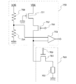
本実施の形態の半導体装置が有するメモリ素子10を図1(A)に示し、抵抗素子20を図1(B)に示す。図1(A)に示したメモリ素子10は、導電層13と、導電層13上のメモリ層12と、メモリ層12上の導電層11とを有する。また、図1(B)に示した抵抗素子20は、導電層23と、導電層23上の抵抗層22と、抵抗層22上の導電層21とを有する。なお、メモリ層12及び抵抗層22は、同一材料からなる。さらに、メモリ素子10は、一定値以上の電圧が印加されることによって、メモリ層12が絶縁破壊され、不可逆的に導電層11及び導電層13を導通させる機能を有する。
A
また、本実施の形態の半導体装置において、メモリ素子10に印加される電圧の最大値を模式的に図1(C)に示し、抵抗素子20に印加される電圧の最大値を模式的に図1(D)に示す。図1(C)、(D)に示すように、メモリ素子10に印加する電圧の最大値は、抵抗素子20に印加する電圧よりも大きい。具体的には、メモリ素子10に印加する電圧の最大値は、メモリ層12が不可逆反応を起こし導電層11及び導電層13を導通させるのに必要な電圧よりも大きく、抵抗素子20に印加する電圧の最大値は、当該電圧よりも小さい。そのため、抵抗素子20の抵抗層22は、メモリ層12と同一材料を適用しながらも、絶縁破壊を起こすことがない。つまり、半導体装置内における抵抗として機能させることができる。
In the semiconductor device of the present embodiment, the maximum value of the voltage applied to the
本実施の形態の半導体装置は、メモリ素子のメモリ層と、抵抗素子の抵抗層とが同一材料によって構成される。つまり、当該メモリ層と、当該抵抗層とを同一工程において形成することが可能である。そのため、当該半導体装置の作製工程を低減することができる。結果として、当該半導体装置の歩留まりを向上させること又は製造コストを低減することができる。また、メモリ層12に用いられる抵抗値の高い材料を用いて抵抗層22を構成することによって、抵抗素子20に必要とされる回路面積を低減することができる。
In the semiconductor device of this embodiment, the memory layer of the memory element and the resistance layer of the resistance element are formed of the same material. That is, the memory layer and the resistance layer can be formed in the same process. Therefore, the manufacturing process of the semiconductor device can be reduced. As a result, the yield of the semiconductor device can be improved or the manufacturing cost can be reduced. In addition, by forming the
さらに、メモリ素子のメモリ層及び抵抗素子の抵抗層のみならず、メモリ素子及び抵抗素子を全て同一材料によって構成することもできる。つまり、メモリ素子10の導電層11及び抵抗素子20の導電層21を同一材料によって形成し、且つメモリ素子10の導電層13及び抵抗素子20の導電層23を同一材料によって形成することができる。これにより、導電層11及び導電層21、導電層13及び導電層23を同一工程によって形成することができるため、半導体装置の作製工程を低減することができる。なお、メモリ素子及び抵抗素子が有する一対の電極のどちらか一方を同一材料によって形成することもできる。
Furthermore, not only the memory layer of the memory element and the resistance layer of the resistance element, but also the memory element and the resistance element can all be made of the same material. That is, the
なお、本実施の形態の内容又は該内容の一部は、他の実施の形態又は実施例の内容又は該内容の一部と自由に組み合わせることが可能である。 Note that the contents of this embodiment or part of the contents can be freely combined with the contents of other embodiments or examples or part of the contents.
(実施の形態2)
本実施の形態では、同一基板上にメモリ素子及び抵抗素子を有する半導体装置及びその作製方法の一例について図2乃至図6を参照しながら説明する。具体的には、メモリ回路と、質問器による情報の2重読み取りを防止するフラグ回路とを有する半導体装置について説明する。
(Embodiment 2)
In this embodiment, an example of a semiconductor device including a memory element and a resistance element over the same substrate and a manufacturing method thereof will be described with reference to FIGS. Specifically, a semiconductor device including a memory circuit and a flag circuit that prevents double reading of information by an interrogator will be described.
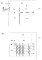
<メモリ回路>
本実施の形態の半導体装置が有するメモリ回路の回路構成例を図2(A)に示す。図2(A)に示したメモリ回路は、トランジスタ101、容量素子102及びメモリ素子103を有する。さらに、トランジスタ101は、ゲート電極が制御端子104に電気的に接続され、第1電極が入出力端子105に電気的に接続される。容量素子102は、一方の電極がトランジスタ101の第2電極に電気的に接続され、他方の電極が接地される。メモリ素子103は、一方の電極がトランジスタ101の第1電極及び容量素子102の一方の電極に電気的に接続され、他方の電極が接地される。
<Memory circuit>
An example of a circuit configuration of a memory circuit included in the semiconductor device of this embodiment is illustrated in FIG. The memory circuit illustrated in FIG. 2A includes a
図2(A)に示したメモリ回路において、トランジスタ101のスイッチングは、制御端子104から入力される信号によって制御され、トランジスタ101がオン時にメモリ素子103へのデータの書き込み又は読み出しが行われる。書き込みの際には、メモリ素子103の一方の電極に入出力端子105から信号が入力される。この際、メモリ素子103に印加される電圧が書き込み電圧以上であれば、メモリ素子103にデータが書き込まれる。また、メモリ素子103の一方の電極の電位が入出力端子105へと出力されることにより、データの読み出しが行われる。なお、容量素子102は、メモリ素子103への書き込み歩留まり(書き込みが成功する確率)を向上させるために設けられている。つまり、本実施の形態のメモリ回路は、容量素子102がなくても機能し得る。
In the memory circuit illustrated in FIG. 2A, switching of the
<フラグ回路>
本実施の形態の半導体装置が有するフラグ回路の回路構成例を図2(B)に示す。なお、フラグ回路は、当該半導体装置から情報を読み出した後に、再度読み出すこと(2重読み出し)を防止する機能を有する。具体的には、当該フラグ回路は、信号が入力され且つ当該信号を一定時間保持することができる揮発性メモリである。図2(B)に示したフラグ回路は、トランジスタ151、容量素子152及び抵抗素子153を有する。さらに、トランジスタ151は、ゲート電極が制御端子154に電気的に接続され、第1電極が入力端子155に電気的に接続される。容量素子152は、一方の電極がトランジスタ151の第2電極及び出力端子156に電気的に接続され、他方の電極が接地される。抵抗素子153は、一方の電極がトランジスタ151の第2電極、容量素子152の一方の電極及び出力端子156に電気的に接続され、他方の電極が接地される。
<Flag circuit>
An example of a circuit configuration of the flag circuit included in the semiconductor device of this embodiment is illustrated in FIG. Note that the flag circuit has a function of preventing reading (double reading) after reading information from the semiconductor device. Specifically, the flag circuit is a volatile memory that receives a signal and can hold the signal for a certain period of time. The flag circuit illustrated in FIG. 2B includes a
なお、フラグ回路の後段(出力端子156の接続先)には、バッファ(図示しない)が設けられている。当該バッファは、フラグ回路の出力信号(ノードAの電位)がある一定値以上の時に高電圧電位を出力し、該一定値未満の時に低電圧電位を出力する。例えば、インバータを直列に2段接続することによって当該バッファを構成することができる。この時、出力端子156は当該インバータを構成するトランジスタのゲート電極に電気的に接続されることになる。そのため、出力端子156の先において、信号は当該バッファに入力されるが電気的な接続は終端しているといえる。
A buffer (not shown) is provided at the subsequent stage of the flag circuit (the connection destination of the output terminal 156). The buffer outputs a high voltage potential when the output signal of the flag circuit (potential of the node A) is equal to or higher than a certain value, and outputs a low voltage potential when it is less than the certain value. For example, the buffer can be configured by connecting inverters in two stages in series. At this time, the
図2(B)に示したフラグ回路において、トランジスタ151のオン、オフは、制御端子154から入力される信号によって制御される。なお、当該信号としては、外部の質問器から入力される読み出し信号などが該当する。該読み出し信号によってトランジスタ151がオンすることで、入力端子155から信号がフラグ回路へと入力される。具体的には、容量素子152に電荷が蓄積される。これにより、ノードAの電位が容量素子152に蓄積された電荷に対応した電位となり、出力端子156から後段のバッファに出力される。なお、この時のノードAの電位は、後段のバッファが高電圧電位を出力するのに必要な電位以上の電位である。
In the flag circuit shown in FIG. 2B, on / off of the
次いで、外部の質問器からの読み出し信号が途絶えると、トランジスタ151がオフする。これにより、抵抗素子153を介して接地されているノードAの電位は、接地電位へと低下することになる。ただし、抵抗素子153の抵抗値によって、接地電位に至るまでの時間を制御することができる。具体的には、抵抗素子153の抵抗値を高くすることによって、ノードAの電位の低下を遅くすることができる。一方、ノードAの電位が一定値以下になった場合にフラグ回路の後段に設けられたバッファの出力信号が低電圧電位へと変化する。つまり、抵抗素子153の抵抗値によって、バッファの出力信号の保持時間も制御できることになる。本実施の形態の半導体装置では、外部の質問器から入力される読み出し信号と共に当該バッファの出力信号を参照して、メモリ回路などの読み出し動作を行うように設定する。これにより、外部の質問器から、短時間に複数回の読み出し信号が入力された場合における2重読み出しを防止することができる。
Next, when the readout signal from the external interrogator is interrupted, the
<メモリ回路及びフラグ回路の構成>
本実施の形態の半導体装置が有するメモリ回路及びフラグ回路の構成例について図3及び図4に示す。図3(A)は、メモリ回路の上面図を示し、図3(B)は、フラグ回路の上面図を示している。図4(A)は、図3(A)に示したメモリ回路の上面図のA−B、C−D、E―Fにおける断面図を示し、図4(B)は、図3(B)に示したフラグ回路の上面図のG−H、I―J、K−Lにおける断面図を示している。
<Configuration of memory circuit and flag circuit>
Configuration examples of the memory circuit and the flag circuit included in the semiconductor device of this embodiment are illustrated in FIGS. FIG. 3A shows a top view of the memory circuit, and FIG. 3B shows a top view of the flag circuit. 4A is a cross-sectional view taken along lines AB, CD, and EF in the top view of the memory circuit illustrated in FIG. 3A. FIG. 4B is a cross-sectional view of FIG. FIG. 6 is a cross-sectional view taken along lines GH, IJ, and KL in the top view of the flag circuit shown in FIG.
図3(A)、図4(A)に示したメモリ回路が有するトランジスタ101は、基板300上の半導体層301と、半導体層301上の絶縁層302と、絶縁層302上の導電層303と、導電層303上の絶縁層304及び絶縁層305に設けられた開口部において半導体層301と電気的に接続された導電層306a及び導電層306bとによって構成される。さらに、半導体層301はシリコンを主構成元素とする半導体からなり、チャネル形成領域307a及び不純物領域307b、307cが設けられている。また、導電層306aは、不純物領域307bと接続するように設けられ、導電層306bは、不純物領域307cと接続するように設けられている。トランジスタ101において、絶縁層302はゲート絶縁層として、導電層303はゲート電極として、導電層306a、306bは第1電極又は第2電極として機能する。
A
図3(A)、図4(A)に示したメモリ回路が有する容量素子102は、基板300上のシリコン電極層311と、シリコン電極層311上の絶縁層302と、絶縁層302上の導電層312とによって構成される。なお、シリコン電極層とは、高濃度に不純物元素が導入され且つ結晶化することによって電極として機能させることが可能な低抵抗なシリコン層を指す。また、導電層312は、導電層303と同じ材料からなる。容量素子102において、シリコン電極層311は一方の電極として、絶縁層302は誘電体として、導電層312は他方の電極として機能する。
The
図3(A)、図4(A)に示したメモリ回路が有するメモリ素子103は、基板300上の導電層321と、導電層321上のアモルファスシリコン層322と、アモルファスシリコン層322上の酸化窒化シリコン層323と、酸化窒化シリコン層323上の導電層324とによって構成される。なお、導電層321は導電層303及び導電層312と同じ材料からなり、導電層324は導電層306a、306bと同じ材料からなる。また、本明細書において、酸化窒化シリコンとは、組成として、窒素よりも酸素の含有量が多いものであって、ラザフォード後方散乱法(RBS:Rutherford Backscattering Spectrometry)及び水素前方散乱法(HFS:Hydrogen Forward Scattering)を用いて測定した場合に、組成範囲として酸素が50〜70原子%、窒素が0.5〜15原子%、シリコンが25〜35原子%、水素が0.1〜10原子%の範囲で含まれ、それらの合計が100原子%となるものをいう。メモリ素子103において、導電層321は一方の電極として、アモルファスシリコン層322及び酸化窒化シリコン層323はメモリ層として、導電層324は他方の電極として機能する。
The
図3(B)、図4(B)に示したフラグ回路が有するトランジスタ151は、メモリ回路が有するトランジスタ101と構造が同じである。そのため、ここでは、前述の説明を援用することとする。ただし、開口部の径、各層の幅などの子細な設計条件については同一である必要はなく、フラグ回路が有するトランジスタ151及びメモリ回路が有するトランジスタ101において独立に設計してもよい。
The
図3(B)、図4(B)に示したフラグ回路が有する容量素子152は、メモリ回路が有する容量素子102と構造が同じである。そのため、ここでは、前述の説明を援用することとする。ただし、開口部の径、各層の幅などの子細な設計条件については同一である必要はなく、フラグ回路が有する容量素子152及びメモリ回路が有する容量素子102において独立に設計してもよい。
The
図3(B)、図4(B)に示したフラグ回路が有する抵抗素子153は、基板300上のシリコン電極層351と、シリコン電極層351上のアモルファスシリコン層352と、アモルファスシリコン層352上の酸化窒化シリコン層353と、酸化窒化シリコン層353上の導電層354とによって構成される。なお、シリコン電極層351はメモリ回路におけるシリコン電極層311と同じ材料からなり、導電層354はメモリ回路における導電層306a、306b及び導電層324と同じ材料からなる。抵抗素子153において、シリコン電極層351は一方の電極として、アモルファスシリコン層322及び酸化窒化シリコン層323は抵抗層として、導電層354は他方の電極として機能する。
3B and 4B, the
本実施の形態の半導体装置において、メモリ回路が有するメモリ素子103及びフラグ回路が有する抵抗素子153は共に一対の電極間にアモルファスシリコン層及び酸化窒化シリコン層が設けられた構成を有する。ただし、メモリ素子103と、抵抗素子153とでは、印加される電圧の最大値が異なる。具体的には、メモリ素子103に印加される電圧の最大値は、導電層321と、アモルファスシリコン層322とをシリサイド反応させ、且つ酸化窒化シリコン層を絶縁破壊するのに必要な電圧値(書き込み電圧ともいう)以上であるのに対し、抵抗素子153に印加される電圧の最大値は、書き込み電圧よりも低い。そのため、メモリ回路においては、当該アモルファスシリコン層及び当該酸化窒化シリコン層をメモリ素子のメモリ層として適用し、且つフラグ回路においては、当該アモルファスシリコン層及び当該酸化窒化シリコン層を抵抗素子の抵抗層として適用することができる。
In the semiconductor device of this embodiment, each of the
なお、メモリ素子103においては、アモルファスシリコン層322及び酸化窒化シリコン層323を絶縁破壊することによって、導電層321及び導電層324が導通する。ただし、絶縁破壊は、導電層321及び導電層324に挟まれた全ての領域で発生する必要はない。別言すると、導電層321及び導電層324の間に電流の通路が確保されればよく、アモルファスシリコン層322及び酸化窒化シリコン層323の一部が絶縁破壊されればよい。つまり、メモリ素子103において、導電層321及び導電層324と、メモリ層として機能するアモルファスシリコン層322及び酸化窒化シリコン層323との接触面積が大きければ大きいほど、書き込み歩留まり(書き込みが成功する確率)を向上させることができる。上記点を考慮し、本実施の形態の半導体装置は、メモリ素子103が形成される開口部の径が抵抗素子153が形成される開口部の径よりも大きくなるように設計されている。
Note that in the
また、印加される電圧の最大値が、メモリ素子における書き込み電圧以上であったとしても、アモルファスシリコン層352及び酸化窒化シリコン層353の積層を絶縁破壊させる電圧値以下であれば、抵抗素子153は機能し得る。なぜなら、抵抗素子153は、アモルファスシリコン層352と接する電極としてシリコン電極層351を適用している。そのため、抵抗素子153に対して書き込み電圧に準じる電圧が印加された場合であっても、シリサイド反応が起きない。結果として、抵抗素子153を構成する一対の電極が導通しないからである。なお、抵抗素子の一方の電極としてシリコン電極層を適用し、且つシリコン電極層と接する抵抗層にアモルファスシリコン層を適用すれば、上記の内容は援用できる。例えば、上記の酸化窒化シリコン層353を他の絶縁層と適宜置き換えた構成であっても上記の作用を有する抵抗素子とすることができる。
In addition, even if the maximum value of the applied voltage is equal to or higher than the write voltage in the memory element, the
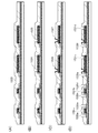
<メモリ回路及びフラグ回路の作製方法>
図3及び図4に示したメモリ回路及びフラグ回路の作製方法の一例について図5及び図6を用いて説明する。具体的には、各々の回路が有する素子をフォトリソグラフィ法を用いて作製する方法について説明する。なお、図3及び図4に示したメモリ回路及びフラグ回路においては、トランジスタ構造及び容量素子構造が共通である。そのため、図5及び図6においてはメモリ回路が有するトランジスタ101、容量素子102及びメモリ素子103並びにフラグ回路が有する抵抗素子153について示す。
<Method for Manufacturing Memory Circuit and Flag Circuit>
An example of a method for manufacturing the memory circuit and the flag circuit illustrated in FIGS. 3 and 4 will be described with reference to FIGS. Specifically, a method for manufacturing an element included in each circuit by a photolithography method will be described. Note that in the memory circuit and the flag circuit shown in FIGS. 3 and 4, the transistor structure and the capacitor element structure are common. Therefore, FIGS. 5 and 6 illustrate the
まず、基板400上に半導体層を成膜する。基板400としては、ガラス基板、石英基板、ステンレス等の金属基板、セラミック基板またはプラスチック基板などを用いることができる。なお、プラスチック基板としては、ポリエチレンテレフタレート(PET)、ポリエチレンナフタレート(PEN)、ポリエーテルサルフォン(PES)、アクリルなどの基板を用いることができる。半導体層は、シリコン(Si)若しくはゲルマニウム(Ge)などの周期表第14族元素からなる元素、シリコンゲルマニウム(SiGe)若しくはガリウムヒ素(GaAs)などの化合物、酸化亜鉛(ZnO)若しくはインジウム(In)及びガリウム(Ga)を含む酸化亜鉛などの酸化物、又は半導体特性を示す有機化合物などの半導体材料を用いて形成することができる。また、これらの半導体材料からなる層の積層構造としてもよい。ここでは半導体層は、シリコンを主構成元素とした層を適用する。なお、半導体層の形成には、プラズマCVD法又はスパッタ法などの薄膜堆積法を用いることができる。また、半導体層は、レーザ結晶化法、RTA(Rapid Thermal Anneal)若しくはファーネスアニール炉を用いた熱結晶化法、又はニッケル(Ni)などの結晶化を助長する金属元素を用いる結晶化法などにより結晶化を行ってもよい。なお、必要があれば、後に完成する薄膜トランジスタのしきい値電圧を制御するために、半導体層に微量に不純物元素を添加してもよい。該不純物元素としては、半導体に対しp型の導電性を与えるボロン(B)又はn型の導電性を与えるリン(P)などを適用することができる。
First, a semiconductor layer is formed over the
次いで、フォトリソグラフィ法を用いて当該半導体層上にレジストを形成する。さらに当該レジストをマスクとして、半導体層を選択的にエッチングし、半導体層402a、402b、402cを形成する(図5(A)参照)。
Next, a resist is formed over the semiconductor layer by a photolithography method. Further, using the resist as a mask, the semiconductor layer is selectively etched to form
次いで、基板400及び半導体層402a、402b、402c上に絶縁層403を成膜する。絶縁層403は、酸化シリコン、窒化シリコン、酸化窒化シリコン、又は窒化酸化シリコンなどの絶縁材料を用いて形成することができる。なお、窒化酸化シリコンとは、その組成として、酸素よりも窒素の含有量が多いものであって、RBS及びHFSを用いて測定した場合に、濃度範囲として酸素が5原子%以上30原子%以下、窒素が20原子%以上55原子%以下、シリコンが25原子%以上35原子%以下、水素が10原子%以上30原子%以下の範囲で含まれ、それらの合計が100原子%となるものをいう。また、これらの絶縁材料からなる層の積層構造としてもよい。なお、絶縁層403は、後にトランジスタが形成される領域においてはゲート絶縁層として利用され、後に容量素子が形成される領域においては一対の電極の間に設けられる誘電体として利用される。また、絶縁層403の成膜には、プラズマCVD法又はスパッタ法などの薄膜堆積法を用いることができる。
Next, the insulating
次いで、フォトリソグラフィ法を用いて、少なくとも半導体層402aを覆うレジストを形成する。さらに該レジストをマスクとして半導体層402b、402cに高濃度の不純物元素を添加し、シリコン電極層404a、404bを形成する(図5(B)参照)。該不純物元素は半導体に対しp型の導電性を与えるボロン(B)又はn型の導電性を与えるリン(P)などを適用することができる。なお、メモリ素子部において後にアシスト容量として用いる容量素子を形成し、且つ当該高濃度に不純物元素を含有する半導体層を電極として適用する場合には、当該半導体層にはP型を与える不純物元素を添加すると好ましい。
Next, a resist that covers at least the
次いで、絶縁層403上に導電層を成膜する。金属単体若しくは合金又は金属元素を含む化合物から選ばれる導電性材料を用いて形成することができる。また、これらの導電性材料からなる層の積層構造としてもよい。なお、当該導電層からは、後にトランジスタのゲート電極が形成されるため、高融点材料を用いることが好ましい。また、当該導電層からは、後にアモルファスシリコン層と接するメモリ素子の電極が形成されるため、シリサイド反応を起こしやすい材料を用いることが好ましい。具体的には、タングステン(W)、チタン(Ti)、モリブデン(Mo)、コバルト(Co)、ハフニウム(Hf)、ニッケル(Ni)、ジルコニウム(Zr)、クロム(Cr)、バナジウム(V)、パラジウム(Pd)、白金(Pt)などの単体、又はこれらの合金、或いはこれらを主成分とする化合物などである。さらに、当該導電層を積層構造とする場合には、上層となる材料層が上述した材料であればよく、絶縁層403側である下層となる材料は任意に選択することができる。なお、当該導電層の成膜には、スパッタ法などの薄膜堆積法を用いることができる。
Next, a conductive layer is formed over the insulating
次いで、フォトリソグラフィ法を用いて、当該導電層上にレジストを形成する。さらに該レジストをマスクとして、導電層405a、405b、405c、405d、405e、405fを形成する。
Next, a resist is formed over the conductive layer by a photolithography method. Further,
次いで、フォトリソグラフィ法を用いて、少なくともシリコン電極層404a、404b及び導電層405b、405c、405d、405e、405fを覆うレジストを形成する。さらに、導電層405aをマスクとして、半導体層402aに不純物元素を添加し、不純物領域406a、406bを形成する(図5(C)参照)。当該不純物元素としては、半導体に対しp型の導電性を与えるボロン(B)又はn型の導電性を与えるリン(P)などを適用することができる。なお、不純物領域406a、406bにおける不純物濃度は、シリコン電極層404a、404bよりも低く、後に形成されるトランジスタのソース領域及びドレイン領域として機能する。
Next, a resist that covers at least the
次いで、絶縁層403及び導電層405a、405b、405c、405d、405e、405f上に絶縁層407を成膜する。絶縁層407は、酸化シリコン、窒化シリコン、酸化窒化シリコン、窒化酸化シリコンなどの絶縁材料を用いて形成することができる。また、これらの絶縁材料からなる膜の積層構造としてもよい。さらに、絶縁層407上に絶縁層408を成膜する。絶縁層408は、酸化シリコン、窒化シリコン、酸化窒化シリコン、窒化酸化シリコン、又はポリイミド、ポリアミド、ポリビニルフェノール、ベンゾシクロブテン、アクリル若しくはエポキシなどの有機材料などの絶縁材料を用いて形成することができる。また、これらの絶縁材料からなる層の積層構造としてもよい。なお、絶縁層407及び絶縁層408の成膜には、プラズマCVD法若しくはスパッタ法などの薄膜堆積法又はスピンコート法などの塗布法を用いることができる。
Next, the insulating
次いで、フォトリソグラフィ法を用いて、絶縁層408上に選択的にレジストを形成する。さらに該レジストをマスクとして、絶縁層407及び絶縁層408を貫通し、導電層405dに達する開口部409a、並びに絶縁層403、絶縁層407及び絶縁層408を貫通し、シリコン電極層404bに達する開口部409bを形成する。なお、開口部409a、409bは、後にメモリ素子又は抵抗素子として利用される領域に設けられる。加えて、当該工程において、後に導電層が設けられる領域の開口部も形成される(図6(A)参照)。
Next, a resist is selectively formed over the insulating
次いで、導電層405d、シリコン電極層404b及び絶縁層408上にアモルファスシリコン層を成膜する。さらに、該アモルファスシリコン層上に酸化窒化シリコン層を成膜する。なお、当該アモルファスシリコン層及び当該酸化窒化シリコン層の成膜には、プラズマCVD法又はスパッタ法などの薄膜堆積法を用いることができる。
Next, an amorphous silicon layer is formed over the
次いで、フォトリソグラフィ法を用いて、当該酸化窒化シリコン層上に選択的にレジストを形成する。さらに該レジストをマスクとして、当該アモルファスシリコン層及び当該酸化窒化シリコン層を選択的にエッチングし、アモルファスシリコン層410a、410b及び酸化窒化シリコン層411a、411bを形成する(図6(B)参照)。
Next, a resist is selectively formed over the silicon oxynitride layer by a photolithography method. Further, the amorphous silicon layer and the silicon oxynitride layer are selectively etched using the resist as a mask to form
次いで、絶縁層408及び酸化窒化シリコン層411a、411b上に導電層を成膜する。該導電層は、金属単体若しくは合金又は金属元素を含む化合物から選ばれる導電性材料を用いて形成することができる。なお、当該導電層の成膜には、スパッタ法などの薄膜堆積法を用いることができる。
Next, a conductive layer is formed over the insulating
次いで、フォトリソグラフィ法を用いて、当該導電層上に選択的にレジストを形成する。さらに、該レジストをマスクとして、当該導電層をエッチングし、導電層412a、412b、412c、412d、412e、412f、412g、412hを形成する(図6(C)参照)。
Next, a resist is selectively formed over the conductive layer by a photolithography method. Further, using the resist as a mask, the conductive layer is etched to form
以上の工程により、メモリ回路が有するトランジスタ101、容量素子102及びメモリ素子103並びにフラグ回路が有する抵抗素子153を作製することができる。なお、上記の作製工程は一例であり、本実施の形態の作製工程は上記工程に限定されない。
Through the above steps, the
本実施の形態の半導体装置は、メモリ素子のメモリ層と、抵抗素子の抵抗層とが同一材料によって構成される。つまり、当該メモリ層と、当該抵抗層とを同一工程において形成することが可能である。そのため、当該半導体装置の作製工程を低減することができる。結果として、当該半導体装置の歩留まりを向上させること又は製造コストを低減することができる。また、メモリ層に用いられる抵抗値の高い材料を抵抗層に用いて抵抗素子を構成することによって、抵抗素子を有する半導体装置の回路面積を低減することができる。 In the semiconductor device of this embodiment, the memory layer of the memory element and the resistance layer of the resistance element are formed of the same material. That is, the memory layer and the resistance layer can be formed in the same process. Therefore, the manufacturing process of the semiconductor device can be reduced. As a result, the yield of the semiconductor device can be improved or the manufacturing cost can be reduced. In addition, by forming a resistance element using a material having a high resistance value used for the memory layer for the resistance layer, a circuit area of a semiconductor device including the resistance element can be reduced.
なお、本実施の形態で述べた内容又は該内容の一部は、他の実施の形態又は実施例の内容又は該内容の一部と自由に組み合わせることが可能である。 Note that the content described in this embodiment or part of the content can be freely combined with the content of another embodiment or example or part of the content.
(実施の形態3)
本実施の形態では、メモリ素子及び抵抗素子を有する半導体装置の一例について図7を参照しながら説明する。具体的には、メモリ回路と、該メモリ回路からの情報の読み出しを行う読み出し回路とを有する半導体装置について説明する。
(Embodiment 3)
In this embodiment, an example of a semiconductor device including a memory element and a resistance element will be described with reference to FIGS. Specifically, a semiconductor device including a memory circuit and a reading circuit that reads information from the memory circuit is described.
<メモリ回路及び読み出し回路>
本実施の形態の半導体装置が有するメモリ回路及び読み出し回路の回路構成例を図7に示す。
<Memory circuit and readout circuit>
FIG. 7 illustrates a circuit configuration example of the memory circuit and the reading circuit included in the semiconductor device of this embodiment.
図7に示すメモリ回路700は、トランジスタ701及びメモリ素子702を有する。さらに、トランジスタ701は、ゲート電極が制御端子703に電気的に接続される。メモリ素子702は、一方の電極がトランジスタ701の一方の電極に電気的に接続され、他方の電極が接地される。
A
図7に示す読み出し回路750は、トランジスタ751、トランジスタ752、抵抗素子753、抵抗素子754及びコンパレータ755を有する。さらに、トランジスタ751は、ゲート電極が接地され、第1電極に電源電圧VDDが与えられる配線(電源線ともいう)に電気的に接続される。トランジスタ752は、ゲート電極が制御端子756に電気的に接続され、第1電極がトランジスタ751の第2電極に電気的に接続され、第2電極がトランジスタ701の第2電極及びコンパレータ755の第1の入力端子に電気的に接続される。抵抗素子753は、一方の電極が電源線に電気的に接続され、他方の電極がコンパレータ755の第2の入力端子に電気的に接続される。抵抗素子754は、一方の電極が抵抗素子753の他方の電極及びコンパレータ755の第2の入力端子に電気的に接続され、他方の電極が接地される。
A
なお、ここでは、p型であり且つゲート電極が接地されているトランジスタ751は、スイッチング素子としてではなく抵抗素子として利用されている。そのため、トランジスタ751を抵抗素子に置き換えることが可能である。また、抵抗素子753及び抵抗素子754の抵抗層としてメモリ素子702のメモリ層と同一材料が適用されている。なお、抵抗素子として利用しているトランジスタ751の抵抗値は、書き込み前後のメモリ素子の抵抗値の間の値をとるように設計する。
Note that here, the
上記構成の回路において読み出し信号が入力されると、制御端子703及び制御端子756からそれぞれトランジスタ701又はトランジスタ752に信号が入力され、両者がオンする。これにより、電源線がトランジスタ751及びメモリ素子702を介して接地される。そのため、電源電圧VDDがトランジスタ751及びメモリ素子702によって分圧された電位がコンパレータ755の第1の入力端子に入力される。また、コンパレータ755の第2の入力端子には、抵抗素子753及び抵抗素子754によって分圧された電位が入力される。ここでは、抵抗素子753及び抵抗素子754の抵抗層は同一材料によって構成されるため、VDD/2程度の電位がコンパレータ755の第2の入力端子に入力されることになる。
When a read signal is input to the circuit having the above structure, a signal is input to the
つまり、メモリ素子702への書き込みが行われていない状態では、コンパレータ755の第1の入力端子に入力される電位が、第2の入力端子に入力される電位よりも高く、メモリ素子702への書き込みが行われている状態では、コンパレータ755の第1の入力端子に入力される電位が、第2の入力端子に入力される電位よりも低くなる。コンパレータ755は、第1の入力端子に入力される電位及び第2の入力端子に入力される電位を比較し、2値の信号として出力する。そのため、コンパレータ755の出力信号によって、メモリ素子702への書き込みの有無が判別できる。
That is, in the state where writing to the
本実施の形態の半導体装置において、電源電圧VDDは、メモリ素子702への書き込み電圧よりも小さい。そのため、抵抗素子753及び抵抗素子754の抵抗層としてメモリ素子702のメモリ層と同一材料を適用することが可能である。当該メモリ層としては、高電圧が印加されることにより、電気伝導特性が大きく増大するという機能を有する層であればどのような構成であってもよい。例えば、実施の形態2で説明したアモルファスシリコン層及び酸化窒化シリコン層の積層を適用することができる。また、アモルファスシリコン層又は酸化窒化シリコン層の単層であってもよい。さらに、当該メモリ層を構成する材料として有機化合物を適用することもできる。
In the semiconductor device of this embodiment, the power supply voltage VDD is lower than the write voltage to the
本実施の形態の半導体装置は、メモリ素子のメモリ層と、抵抗素子の抵抗層とが同一材料によって構成される。つまり、当該メモリ層と、当該抵抗層とを同一工程において形成することが可能である。そのため、当該半導体装置の作製工程を低減することができる。結果として、当該半導体装置の歩留まりを向上させること又は製造コストを低減することができる。また、メモリ層に用いられる抵抗値の高い材料を抵抗層に用いて抵抗素子を構成することによって、抵抗素子を有する半導体装置の回路面積を低減することができる。 In the semiconductor device of this embodiment, the memory layer of the memory element and the resistance layer of the resistance element are formed of the same material. That is, the memory layer and the resistance layer can be formed in the same process. Therefore, the manufacturing process of the semiconductor device can be reduced. As a result, the yield of the semiconductor device can be improved or the manufacturing cost can be reduced. In addition, by forming a resistance element using a material having a high resistance value used for the memory layer for the resistance layer, a circuit area of a semiconductor device including the resistance element can be reduced.
なお、本実施の形態の読み出し回路の構成は、上記の構成に限定されない。 Note that the structure of the reading circuit in this embodiment is not limited to the above structure.
例えば、抵抗素子753又は抵抗素子754のどちらか一方の抵抗層にメモリ素子のメモリ層と同一材料を適用することが可能である。この場合、抵抗素子753の抵抗値を抵抗素子754の抵抗値よりも低くすることが可能になる。抵抗素子753の抵抗値を抵抗素子754の抵抗値よりも低くすると、コンパレータ755の第2の入力端子に入力される電位がVDD/2よりも大きい値となる。そのため、読み出し回路750においてトランジスタ751を省略することができる。なぜなら、トランジスタ751が省略された読み出し回路においては、コンパレータ755の第1の入力端子に対して、メモリ素子702への書き込みが行われている場合はVDD/2程度の電位が入力され、書き込みが行われていない場合は電源電圧VDDに準じる電位が入力されるからである。トランジスタ751を省略することによりメモリ素子702からの情報の読み出しにかかる時間を低減することができる。
For example, the same material as the memory layer of the memory element can be applied to one of the resistance layers of the
また、コンパレータ755の第2の入力端子に入力される電位をVDD/2よりも大きくすることによって、トランジスタ701をp型とすることも可能になる。トランジスタ701をp型とした場合、トランジスタ701においては、コンパレータ755の第1の入力端子と電気的に接続される電極がソース電極となり、メモリ素子702と電気的に接続される電極がドレイン電極となる。そのため、コンパレータ755の第1の入力端子の入力電位が、単に電源電圧VDDを抵抗分圧した値となるのではなく、トランジスタ701のしきい値電圧を加味した電位になる。また、当該しきい値電圧は、トランジスタ701のサイズなどによっては、VDD/2程度となることがある。つまり、トランジスタ701をn型とした場合、コンパレータ755の第1の入力端子に入力される電位の範囲が電源電圧VDD〜接地電位であるのに対し、トランジスタ701をp型とした場合、コンパレータ755の第1の入力端子に入力される電位の範囲が電源電圧VDD〜VDD/2となる可能性がある。端的に言うと、トランジスタ701をp型とすることによって、コンパレータ755の第1の入力端子に入力される電位の範囲が狭くなる。このような場合であっても、コンパレータ755の第2の入力端子に入力される電位をVDD/2よりも大きくすれば、メモリ素子702への信号の書き込みの有無が判別できる。なお、トランジスタ701をp型とすることにより、耐圧が向上し、ゲート絶縁層を薄膜化することができる。これにより、トランジスタ701を有する半導体装置の消費電力を低減することができる。
In addition, when the potential input to the second input terminal of the
なお、本実施の形態の内容又は該内容の一部は、他の実施の形態又は実施例の内容又は該内容の一部と自由に組み合わせることが可能である。 Note that the contents of this embodiment or part of the contents can be freely combined with the contents of other embodiments or examples or part of the contents.
(実施の形態4)
本実施の形態では、同一基板上にメモリ素子及び抵抗素子を有する半導体装置の一例について図8を参照しながら説明する。具体的には、メモリ回路と、該メモリ回路が有するメモリ素子への書き込みが可能な高電圧を生成する昇圧回路とを有する半導体装置について説明する。なお、当該昇圧回路は、リミッタ回路部を有する。該リミッタ回路は、昇圧回路の出力電圧が高すぎる場合に機能し、当該出力電圧を制限する回路である。
(Embodiment 4)
In this embodiment, an example of a semiconductor device including a memory element and a resistance element over the same substrate will be described with reference to FIGS. Specifically, a semiconductor device including a memory circuit and a booster circuit that generates a high voltage capable of writing to a memory element included in the memory circuit will be described. Note that the booster circuit includes a limiter circuit unit. The limiter circuit functions when the output voltage of the booster circuit is too high and limits the output voltage.
<メモリ回路及び昇圧回路>
本実施の形態の半導体装置が有するメモリ回路及び昇圧回路の回路構成例を図8に示す。
<Memory circuit and booster circuit>
FIG. 8 illustrates a circuit configuration example of the memory circuit and the booster circuit included in the semiconductor device of this embodiment.
図8に示すメモリ回路は、図7に示したメモリ回路の構成と同じである。そのため、ここでは、実施の形態3の説明を援用することとする。 The memory circuit shown in FIG. 8 has the same configuration as the memory circuit shown in FIG. Therefore, here, the description of Embodiment 3 is incorporated.
図8に示す昇圧回路800は、昇圧部810及びリミッタ回路部820を有する。昇圧部810は、出力端子がトランジスタ701の第1電極に電気的に接続される。また、昇圧部810からは、昇圧電圧VHHが出力される。なお、昇圧部810の構成は特定の構成に限定されず、入力電圧を昇圧することができる構成であればどのような構成であってもよい。例えば、昇圧部810は、ディクソンタイプの回路によって構成することができる。リミッタ回路部820は、抵抗素子821、抵抗素子822、抵抗素子823、抵抗素子824及びコンパレータ825を有する。さらに、コンパレータ825は、出力端子が昇圧部810の入力端子に電気的に接続される。抵抗素子821は、一方の電極が昇圧部810の出力端子に電気的に接続され、他方の電極がコンパレータ825の第1の入力端子に電気的に接続される。抵抗素子822は、一方の電極が抵抗素子821の他方の電極及びコンパレータ825の第1の入力端子に電気的に接続され、他方の電極が接地される。抵抗素子823は、一方の電極が電源線に電気的に接続され、他方の電極がコンパレータ825の第2の入力端子に電気的に接続される。抵抗素子824は、一方の電極が抵抗素子823の他方の電極及びコンパレータ825の第2の入力端子に電気的に接続され、他方の電極が接地される。
A
なお、昇圧電圧VHHは、昇圧部810によって昇圧された電圧であり、電源電圧VDDよりも高い電位である。また、抵抗素子821の抵抗値は、抵抗素子822、抵抗素子823及び抵抗素子824の抵抗値よりも高く、抵抗素子822、抵抗素子823及び抵抗素子824の抵抗値は同程度である。具体的には、抵抗素子821の抵抗値は、抵抗素子822〜824の5〜10倍である。
Note that the boosted voltage VHH is a voltage boosted by the
上記構成の回路において書き込み信号が入力されると、昇圧部810においてメモリ素子702への書き込みに必要な電圧(昇圧電圧VHH)が生成される。ただし、昇圧電圧VHHは、メモリ回路700のみならず、リミッタ回路部820にも入力される。具体的には、抵抗素子821の一方の電極に昇圧電圧VHHが入力される。そして、抵抗素子821及び抵抗素子822によって分圧された電圧がコンパレータ825の第1の入力端子に入力される。また、コンパレータ825の第2の入力端子には、抵抗素子823及び抵抗素子824によって分圧された電圧が入力される。なお、ここでは、コンパレータ825の第2の入力端子に入力される電圧は、VDD/2程度の一定値をとる。コンパレータ825は、昇圧電圧VHHが高すぎる場合に機能し、昇圧電圧VHHの出力を制御することができる。
When a write signal is input to the circuit having the above structure, a voltage (boosted voltage VHH) necessary for writing to the
本実施の形態の半導体装置において、電源電圧VDDは、メモリ素子702への書き込み電圧よりも小さい。そのため、抵抗素子823及び抵抗素子824の抵抗層としてメモリ素子702のメモリ層と同一材料を適用することが可能である。
In the semiconductor device of this embodiment, the power supply voltage VDD is lower than the write voltage to the
本実施の形態の半導体装置は、メモリ素子のメモリ層と、抵抗素子の抵抗層とが同一材料によって構成される。つまり、当該メモリ層と、当該抵抗層とを同一工程において形成することが可能である。そのため、当該半導体装置の作製工程を低減することができる。結果として、当該半導体装置の歩留まりを向上させること又は製造コストを低減することができる。また、メモリ層に用いられる抵抗値の高い材料を抵抗層に用いて抵抗素子を構成することによって、抵抗素子を有する半導体装置の回路面積を低減することができる。 In the semiconductor device of this embodiment, the memory layer of the memory element and the resistance layer of the resistance element are formed of the same material. That is, the memory layer and the resistance layer can be formed in the same process. Therefore, the manufacturing process of the semiconductor device can be reduced. As a result, the yield of the semiconductor device can be improved or the manufacturing cost can be reduced. In addition, by forming a resistance element using a material having a high resistance value used for the memory layer for the resistance layer, a circuit area of a semiconductor device including the resistance element can be reduced.
なお、本実施の形態の昇圧回路の構成は、上記の構成に限定されない。 Note that the structure of the booster circuit in this embodiment is not limited to the above structure.
例えば、抵抗素子821の抵抗値が抵抗素子822の抵抗値よりも高く、抵抗素子822にメモリ素子702への書き込み電圧以上の電圧が印加されない場合は、抵抗素子822の抵抗層としてもメモリ素子702のメモリ層と同一材料を適用することが可能である。
For example, when the resistance value of the
また、実施の形態2で示したように、メモリ素子702のメモリ層をアモルファスシリコン層及び酸化窒化シリコン層の積層とし、且つ該アモルファスシリコン層と接する電極をシリコン電極層とした構成である場合、抵抗素子821の抵抗層としてもメモリ素子702のメモリ層と同一材料を適用することが可能である。ただし、この場合は抵抗素子821に印加される電圧の最大値が、アモルファスシリコン層及び酸化窒化シリコン層の積層を絶縁破壊する電圧以下である必要がある。このように、抵抗素子821又は抵抗素子822の抵抗層としてメモリ素子702のメモリ層と同一材料を適用することによって、さらに半導体装置の歩留まりを向上させること、製造コストを低減すること、又は回路面積を低減することができる。
Further, as shown in Embodiment Mode 2, when the memory layer of the
なお、本実施の形態の内容又は該内容の一部は、他の実施の形態又は実施例の内容又は該内容の一部と自由に組み合わせることが可能である。 Note that the contents of this embodiment or part of the contents can be freely combined with the contents of other embodiments or examples or part of the contents.
(実施の形態5)
本実施の形態では、無線通信機能を有する半導体装置の一例について図9及び図10を参照しながら説明する。
(Embodiment 5)
In this embodiment, an example of a semiconductor device having a wireless communication function will be described with reference to FIGS.
図9に無線通信機能を有する半導体装置の構成ブロック図を示す。 FIG. 9 shows a block diagram of a semiconductor device having a wireless communication function.
半導体装置900は、交流電圧を生成するアンテナ901と、交流電圧を整流し、内部電圧Vinを生成する整流回路902と、アンテナ901で生成された交流電圧から信号を復調し、内部信号を生成する復調回路903と、整流回路902で生成された内部電圧Vinが大きい場合に機能し、共振周波数を変化させることにより、半導体装置に入力される信号を減少させる保護回路904と、整流回路902において生成された内部電圧Vinを定電圧化して電源電圧VDDとして出力する定電圧回路905と、定電圧回路905で生成された電源電圧VDDを用いてクロック信号CLKを生成する発振回路906と、定電圧回路905で生成された電源電圧VDD、発振回路906で生成されたクロック信号CLK及び復調回路903で生成された復調信号を用いた信号の解析、並びに応答信号の生成を行う論理回路907と、電源電圧VDDの立ち上がりを利用して論理回路907の初期化信号を生成するリセット回路908と、論理回路907からの信号を変調し、アンテナ901に変調信号を出力する変調回路909と、論理回路907と情報のやりとりを行うメモリ回路910及びフラグ回路911と、を有する。
The
メモリ回路910の構成ブロック図を図10(A)に示す。図10(A)に示すメモリ回路910は、メモリセルアレイ921、カラムデコーダ922、ローデコーダ923、インターフェイス924及び昇圧回路925などを有する。
A block diagram of the
さらに、図10(A)に示したメモリ回路が有するメモリセルアレイ921の具体的な回路構成例を図10(B)に示す。メモリセルアレイ921は、m行n列に配列した複数のメモリセル931と、m本のワード線932と、n本のビット線933とを有する(m、nは自然数)。なお、i行j列に配列されたメモリセル931は、ゲート電極が第iのワード線に電気的に接続され、第1電極が第jのビット線に電気的に接続されたトランジスタ934と、一方の電極がトランジスタ934の第2電極に電気的に接続され、他方の電極が固定電位線に電気的に接続されたメモリ素子935とを有する(iはm以下の自然数、jはn以下の自然数である)。なお、本実施の形態では当該固定電位線には、接地電位が与えられているとする。さらに、メモリ素子935と並列に容量素子を設けてもよい。これにより、メモリ素子935への書き込み歩留まり(書き込みが成功する確率)を向上させることができる。
Further, FIG. 10B illustrates a specific circuit configuration example of the
本実施の形態のメモリ回路910のインターフェイス924には外部から書き込み信号(WE)、読み出し信号(RE)、アドレス信号(ADDRESS)、データ信号(DATA)等が入力される。これらの外部信号は、インターフェイス924を介して、カラムデコーダ922及びローデコーダ923に入力される。カラムデコーダ922及びローデコーダ923は、入力信号に基づき、複数のワード線及び複数のビット線の電位を制御する。具体的には、ローデコーダ923によって各メモリセル931に設けられたトランジスタ934のオン、オフが制御され、カラムデコーダ922によって各メモリセル931に設けられたメモリ素子935への情報の書き込み又は読み出しが行われる。
A write signal (WE), a read signal (RE), an address signal (ADDRESS), a data signal (DATA), and the like are input to the
i行j列に配置されたメモリセル931への情報の書き込み動作について以下に述べる。まず、ローデコーダ923によって、第i行に配列したメモリセルが有するトランジスタがオンする。また、カラムデコーダ922によって第jのビット線の電位が上昇する。なお、第jのビット線に与えられる電位は、昇圧回路925において昇圧され、メモリ素子935への書き込みが可能な昇圧電圧VHHである。そのため、i行j列に配置されたメモリセル931が有するメモリ素子935には高電圧が印加され、抵抗値が大幅に変化する。このメモリ素子935の大幅な抵抗値の変化が情報の書き込みに相当する。
An operation of writing information to the
また、i行j列に配列されたメモリセル931からの情報の読み出しについては、実施の形態3で説明したような方法を用いることができる。つまり、i行j列に配列されたメモリ素子935を構成要素とする分圧回路を構成し、当該分圧回路の出力信号を判別することにより情報の書き込み有無を判別することができる。
For reading out information from the
本実施の形態の半導体装置は、上記実施の形態で示したメモリ回路と、上記実施の形態で示したフラグ回路、読み出し回路及び昇圧回路とを有する。メモリ回路は、メモリ素子を有し、フラグ回路、読み出し回路及び昇圧回路の少なくとも一つは、当該メモリ素子のメモリ層を抵抗層とした抵抗素子を有する。本実施の形態の半導体装置では、メモリ素子及び抵抗素子が同一工程によって形成される。そのため、当該半導体装置の作製工程を低減することができる。結果として、当該半導体装置の歩留まりを向上させること又は製造コストを低減することができる。また、メモリ層に用いられる抵抗値の高い材料を抵抗層に用いて抵抗素子を構成することによって、抵抗素子を有する半導体装置の回路面積を低減することができる。 The semiconductor device of this embodiment includes the memory circuit described in the above embodiment, and the flag circuit, the read circuit, and the booster circuit described in the above embodiment. The memory circuit includes a memory element, and at least one of the flag circuit, the read circuit, and the booster circuit includes a resistance element in which the memory layer of the memory element is a resistance layer. In the semiconductor device of this embodiment, the memory element and the resistance element are formed by the same process. Therefore, the manufacturing process of the semiconductor device can be reduced. As a result, the yield of the semiconductor device can be improved or the manufacturing cost can be reduced. In addition, by forming a resistance element using a material having a high resistance value used for the memory layer for the resistance layer, a circuit area of a semiconductor device including the resistance element can be reduced.
なお、本実施の形態の内容又は該内容の一部は、他の実施の形態又は実施例の内容又は該内容の一部と自由に組み合わせることが可能である。 Note that the contents of this embodiment or part of the contents can be freely combined with the contents of other embodiments or examples or part of the contents.
(実施の形態6)
本実施の形態では、無線通信機能を有する半導体装置の具体的な構成例について、図11乃至図13を参照しながら説明する。
(Embodiment 6)
In this embodiment, a specific structural example of a semiconductor device having a wireless communication function will be described with reference to FIGS.
図11(A)に示す半導体装置は、基板1100と、基板1100上に設けられた素子部1101と、素子部1101に電気的に接続されたアンテナ1102と、を有する。
A semiconductor device illustrated in FIG. 11A includes a
素子部1101は、メモリ素子及び抵抗素子などの複数の素子によって構成され、外部から受信した信号を処理する機能を有する。アンテナ1102は、半導体装置のデータの伝送を行う機能を有する。
The
図11(B)に図11(A)に示した半導体装置のA−Bにおける断面図を示す。基板1100上に設けられた素子層1104と、基板1100及び素子層1104上に設けられた絶縁層1103と、絶縁層1103上に設けられたアンテナ1102として機能する導電層1105と、素子層1104に接続された導電層1106と、を有する。
FIG. 11B is a cross-sectional view taken along line AB of the semiconductor device illustrated in FIG. An
なお、図11(B)の構成において、導電層1106と同じ層にアンテナ1102として機能する導電層1105を設けているが、導電層1105及び導電層1106を別の層に設けることも可能である。つまり、素子部1101を設けた後、素子部1101を覆うように別途絶縁層を設け、該絶縁層上に導電層1105を設ける構成とすることもできる。
Note that although the
また、無線通信機能を有する半導体装置の構成は、図11の構成に限定されない。当該半導体装置の他の構成例について図12を用いて説明する。 Further, the structure of the semiconductor device having a wireless communication function is not limited to the structure in FIG. Another example of the structure of the semiconductor device is described with reference to FIGS.
図12(A)に示す半導体装置は、基板1200と、基板1200上に設けられた素子部1201と、素子部1201に電気的に接続されたアンテナ1202と、を有する。
A semiconductor device illustrated in FIG. 12A includes a
図11の構成と同様に素子部1201は、メモリ素子及び抵抗素子などの複数の素子によって構成され、外部から受信した信号を処理する機能を有する。アンテナ1202は、半導体装置におけるデータの伝送を行う機能を有する。
Similar to the configuration in FIG. 11, the
図12(B)に図12(A)に示した半導体装置のC−Dにおける断面図を示す。基板1200と、基板1200の上に設けられたアンテナ1202となる導電層1211a及び樹脂1209と、導電層1211bの上に設けられた導電性粒子を含む層1208と、樹脂1209及び導電性粒子を含む層1208の上に設けられた導電層1206と、導電層1206上に設けられた素子層1204を有する素子部1201と、素子部1201上に設けられた基板1203と、を有する。
FIG. 12B is a cross-sectional view taken along line CD of the semiconductor device illustrated in FIG. A
図12の構成の場合、基板1203に端子部として機能する導電層1206が設けられる。そして、導電層1206と導電層1211bとが導電性粒子を含む層1208を介して電気的に接続するように、素子層1204及び導電層1206が設けられた基板1203とアンテナ1202が設けられた基板1200とが樹脂1209によって貼り合わされている。
In the case of the structure in FIG. 12, a
本実施の形態において、図11の素子部1101及び図12の素子部1201を構成するメモリ素子のメモリ層及び抵抗素子の抵抗層は、上記実施の形態で説明したように同一材料によって構成される。つまり、メモリ素子と、抵抗素子とを同一工程において形成することが可能である。そのため、当該半導体装置の作製工程を低減することができる。結果として、当該半導体装置の歩留まりを向上させること又は製造コストを低減することができる。また、メモリ層に用いられる抵抗値の高い材料を抵抗層に用いて抵抗素子を構成することによって、抵抗素子を有する半導体装置の回路面積を低減することができる。
In this embodiment mode, the memory layer of the memory element and the resistance layer of the resistance element which form the
さらに、図11の素子部1101及び図12の素子部1201は、予め大きな面積の基板上に複数形成し、その後、分断することによって作製することで、製造コストを低減することができる。このときに用いる図11の基板1100、図12の基板1200及び基板1203としては、ガラス基板、石英基板、セラミック基板、金属基板(例えばステンレス基板など)、または半導体基板(例えばシリコン基板など)などを適用することができる。他にもプラスチック基板として、ポリエチレンテレフタラート(PET)、ポリエチレンナフタレート(PEN)、ポリエーテルサルフォン(PES)、アクリルなどの可撓性基板等を適用することができる。
Further, a plurality of the
なお、図11の素子部1101及び図12の素子部1201に含まれる複数のトランジスタ、メモリ素子及び抵抗素子などは、同じ層に設ける構成に限定されない。各種の素子を複数の層に形成した構成とすることもできる。なお、複数の層に図11の素子部1101及び図12の素子部1201を形成する際には、層間絶縁層が設けられる。該層間絶縁層の材料としては、エポキシ樹脂やアクリル樹脂等の樹脂材料、透過性を有するポリイミド樹脂等の樹脂材料、シロキサン樹脂等のシロキサン材料を有する化合物材料、水溶性ホモポリマーと水溶性共重合体を含む材料、無機材料を適用することができ、また、これらの材料を複数種選択して積層構造とすることもできる。シロキサン材料とは、Si−O−Si結合を含む材料に相当する。シロキサンは、シリコン(Si)と酸素(O)との結合で骨格構造が構成される。置換基として、有機基(例えば、アルキル基、アリール基)やフルオロ基を用いてもよい。有機基は、フルオロ基を有していてもよい。また、層間絶縁層は、CVD法、スパッタ法、SOG法、液滴吐出法、スクリーン印刷法等により、形成することができる。
Note that the plurality of transistors, memory elements, resistance elements, and the like included in the
また、層間絶縁層の材料として、層間で発生する寄生容量の減少を目的として、低誘電率材料を適用することが好適である。寄生容量が減少すれば、半導体装置の高速動作を実現し、且つ低消費電力化を実現することができる。 In addition, as a material for the interlayer insulating layer, it is preferable to apply a low dielectric constant material for the purpose of reducing the parasitic capacitance generated between the layers. If the parasitic capacitance is reduced, high-speed operation of the semiconductor device can be realized, and low power consumption can be realized.
図11の導電層1105及び導電層1106、図12の導電層1206及び導電層1211a、1211bは、CVD法、スパッタ法、スクリーン印刷及びグラビア印刷等の印刷法、液滴吐出法、ディスペンサ法、またはメッキ法等を用いて形成することができる。また、図11の導電層1105及び導電層1106、図12の導電層1206及び導電層1211a、1211bとしては、アルミニウム(Al)、チタン(Ti)、銀(Ag)、銅(Cu)、金(Au)、白金(Pt)、ニッケル(Ni)、パラジウム(Pd)、タンタル(Ta)、モリブデン(Mo)から選択された元素を主成分とする合金材料又は化合物材料で形成することができる。さらに、それらの単層構造または積層構造で形成することができる。
The
例えば、スクリーン印刷法を用いて図11の導電層1105及び導電層1106、図12の導電層1206及び導電層1211a、1211bを形成する場合には、粒径が数nmから数十μmの導電体粒子を有機樹脂に溶解または分散させた導電性のペーストを選択的に印刷することによって設けることができる。導電体粒子としては、銀(Ag)、金(Au)、銅(Cu)、ニッケル(Ni)、白金(Pt)、パラジウム(Pd)、タンタル(Ta)、モリブデン(Mo)およびチタン(Ti)等のいずれか一つ以上の金属粒子やハロゲン化銀の微粒子、または分散性ナノ粒子を用いることができる。また、導電性ペーストに含まれる有機樹脂は、金属粒子のバインダー、溶媒、分散剤および被覆材として機能する有機樹脂から選ばれた一つまたは複数を用いることができる。代表的には、エポキシ樹脂、シリコーン樹脂等の有機樹脂が挙げられる。また、導電層の形成において、焼成工程は導電性のペーストを押し出した後に行うことが好ましい。例えば、導電性のペーストの材料として、銀を主成分とする微粒子(例えば粒径1nm以上100nm以下)を用いる場合、150℃以上300℃以下の温度範囲で焼成することにより硬化させて導電層を得ることができる。また、微粒子として、はんだや鉛フリーのはんだを主成分とする微粒子を用いてもよく、この場合は粒径20μm以下の微粒子を用いることが好ましい。はんだや鉛フリーはんだを用いることにより、低コストで製造することができる。
For example, when the
また、半導体装置の構成として、素子部が形成された基板をそのまま活用する例を図11及び図12において示したが、当該半導体装置の構成は、これに限定されない。素子部が形成された基板とは異なる基板を用いて半導体装置を構成する例について図13を用いて説明する。 In addition, although an example in which a substrate on which an element portion is formed is used as it is as a configuration of a semiconductor device is shown in FIGS. 11 and 12, the configuration of the semiconductor device is not limited to this. An example in which the semiconductor device is formed using a substrate different from the substrate over which the element portion is formed will be described with reference to FIGS.
図13(A)に示すように、素子部1311が形成された基板1310において、基板1310上の素子部1311を剥離する。さらに、図13(B)に示すように剥離した素子部1311を基板1310とは別の基板1313に貼り合わせた構成とすることもできる。なお、基板1313としては、例えば可撓性基板などを適用することができる。
As shown in FIG. 13A, in the
基板1310からの素子部1311の剥離は、耐熱性の高い基板1310と素子部1311の間に金属酸化層を設け、当該金属酸化層を結晶化により脆弱化して、素子部1311を剥離する方法、耐熱性の高い基板1310と素子部1311の間に水素を含むアモルファスシリコン層を設け、レーザ光の照射またはエッチングにより当該アモルファスシリコン層を除去することで、素子部1311を剥離する方法、又は素子部1311が形成された耐熱性の高い基板1310を機械的に削除または溶液やCF3等のガスによるエッチングで除去することで、素子部1311を切り離す方法等を用いて行うことができる。
The
また、上記記載の方法以外にも、基板1310と素子部1311の間に剥離層として機能する金属層(例えば、タングステン(W)、モリブデン(Mo)、チタン(Ti)、タンタル(Ta)、コバルト(Co))、金属酸化層(例えば、タングステン酸化物、モリブデン酸化物、チタン酸化物、タンタル酸化物、コバルト酸化物)または金属層と金属酸化層との積層構造を設け、基板1310と、素子部1311とを物理的手段を用いて剥離することも可能である。また、他にも選択的に開口部を形成して剥離層を露出させた後に、フッ化ハロゲン(例えば、ClF3)等のエッチング剤によって剥離層の一部を除去した後に、基板1310から素子部1311を物理的に剥離することもできる。
In addition to the method described above, a metal layer functioning as a separation layer between the
また、剥離した素子部1311の基板1313への貼り付けは、市販の接着剤を用いればよく、例えば、エポキシ樹脂系接着剤や樹脂添加剤等の接着剤を用いればよい。
The peeled
上記のように、素子部1311を基板1313に貼り合わせて半導体装置を作製することにより、薄くて軽く、落下した場合にも壊れにくい半導体装置を提供することができる。また、基板1313として可撓性を有する基板を適用すると、曲面や異形の形状上に貼り合わせることが可能となり、多種多様の用途が実現する。例えば、図13(C)に示すように、薬の瓶のような曲面上に、半導体装置1314を密着して貼り合わせることができる。さらに、基板1310を再利用することにより、半導体装置の製造コストを低減することができる。
As described above, by manufacturing the semiconductor device by attaching the
なお、本実施の形態の内容又は該内容の一部は、他の実施の形態又は実施例の内容又は該内容の一部と自由に組み合わせることが可能である。 Note that the contents of this embodiment or part of the contents can be freely combined with the contents of other embodiments or examples or part of the contents.
(実施の形態7)
本実施の形態では、可撓性を有する半導体装置の構成例について、図14を参照しながら説明する。
(Embodiment 7)
In this embodiment, a structural example of a flexible semiconductor device is described with reference to FIGS.
図14(A)に示す半導体装置は、可撓性を有する保護層1401と、アンテナ1404が設けられた可撓性を有する保護層1403と、剥離プロセスにより形成する素子部1402とを張り合わされることによって作製される。保護層1403上に設けられたアンテナ1404は、素子部1402に電気的に接続する。図14においては、アンテナ1404は保護層1403上にのみ設けられているが、アンテナ1404を保護層1401上にも設けることもできる。また、素子部1402と保護層1401、1403の間には、窒化シリコン層などからなるバリア層を形成することにより、素子部1402が汚染されることなく、信頼性を向上させた半導体装置を提供することができる。
In the semiconductor device illustrated in FIG. 14A, a flexible
素子部1402と、アンテナ1404とは、異方性導電層を用いてUV処理または超音波処理を行うことによって電気的に接続させることができる。ただし、接続方法はこれに限定されず、さまざまな方法を用いることができる。
The
図14(B)は、図14(A)に示した半導体装置の断面図を示している。保護層1401、1403に挟まれた素子部1402の厚さは、5μm以下、好ましくは0.1μm〜3μmの厚さを有するように形成するとよい。また、保護層1401、1403を重ねたときの厚さをdとしたとき、保護層1401、1403の厚さは、好ましくは(d/2)+30μmから(d/2)−30μm、さらに好ましくは(d/2)+10μmから(d/2)−10μmとする。また、保護層1401、1403の厚さは10μm〜200μmであることが望ましい。さらに、素子部1402の面積は5mm角(25mm2)以下であり、望ましくは0.3mm角〜4mm角(0.09mm2〜16mm2)の面積を有するとよい。
FIG. 14B is a cross-sectional view of the semiconductor device illustrated in FIG. The
保護層1401、1403は、有機樹脂材料で形成されているため、折り曲げに対して強い特性を有する。また、剥離プロセスにより形成した素子部1402自体も、折り曲げに対して強い特性を有する。そして、素子部1402と、保護層1401、1403とは空隙がないように、密着させることができるため、完成した半導体装置自体も折り曲げに対して強い特性を有する。このような保護層1401、1403で囲われた素子部1402は、他の個体物の表面または内部に配置してもよいし、紙の中に埋め込んでもよい。
Since the
次に剥離プロセスにより形成する素子部を、曲面を有する基板に貼る場合について説明する。 Next, a case where an element portion formed by a peeling process is attached to a substrate having a curved surface will be described.
図14(C)に示すように、剥離プロセスにより形成した素子部におけるトランジスタの一は、第1電極1405、第2電極1406およびゲート電極1407を有する。また、電流が流れる方向1410と、基板が弧を描く方向は垂直に配置されている。このような配置にすれば、基板が折り曲げられて、基板が弧を描いても、トランジスタへの応力の影響が少なく、素子部1402に含まれるトランジスタの特性の変動を抑制することができる。
As shown in FIG. 14C, one of the transistors in the element portion formed by the separation process includes a
また、トランジスタが存在する領域の面積を素子部1402全体の面積に対して、1%〜50%(好ましくは1〜30%)にすることにより、応力を起因とする素子の破壊を防止することができる。
In addition, by setting the area of the region where the transistor exists to 1% to 50% (preferably 1 to 30%) of the entire area of the
なお、本実施の形態の内容又は該内容の一部は、他の実施の形態又は実施例の内容又は該内容の一部と自由に組み合わせることが可能である。 Note that the contents of this embodiment or part of the contents can be freely combined with the contents of other embodiments or examples or part of the contents.
(実施の形態8)
本実施の形態では、半導体装置の使用例について図15を参照しながら説明する。
(Embodiment 8)
In this embodiment, a usage example of a semiconductor device will be described with reference to FIGS.
図15に示すように、半導体装置の用途は広範囲にわたるが、例えば、紙幣、硬貨、有価証券類、無記名債券類、証書類(運転免許証や住民票等、図15(A)参照)、記録媒体(DVDソフトやビデオテープ等、図15(B)参照)、包装用容器類(包装紙やボトル等、図15(C)参照)、乗り物類(自転車等、図15(D)参照)、身の回り品(鞄や眼鏡等)、食品類、植物類、動物類、人体、衣類、生活用品類、または電子機器(液晶表示装置、EL表示装置、テレビジョン受像機、または携帯電話)等の物品、若しくは各物品に取り付ける荷札(図15(E)、図15(F)参照)等に設けて使用することができる。 As shown in FIG. 15, the semiconductor device has a wide range of uses. For example, banknotes, coins, securities, bearer bonds, certificate documents (driver's license, resident's card, etc., see FIG. 15A), record Medium (DVD software, video tape, etc., see FIG. 15 (B)), packaging containers (wrapping paper, bottles, etc., see FIG. 15 (C)), vehicles (bicycles, etc., see FIG. 15 (D)), Items such as personal items (such as bags and glasses), foods, plants, animals, human bodies, clothing, daily necessities, or electronic devices (liquid crystal display devices, EL display devices, television receivers, or mobile phones) Alternatively, it can be used by being provided on a tag (see FIGS. 15E and 15F) attached to each article.
半導体装置1500は、プリント基板に実装、表面に貼る、または埋め込むことにより、物品に固定される。例えば、本であれば紙に埋め込む、または有機樹脂からなるパッケージであれば当該有機樹脂に埋め込み、各物品に固定される。半導体装置1500は、小型、薄型、軽量を実現するため、物品に固定した後もその物品自体のデザイン性を損なうことがない。また、紙幣、硬貨、有価証券類、無記名債券類、または証書類等に半導体装置1500を設けることにより、認証機能を設けることができ、この認証機能を活用すれば、偽造を防止することができる。また、包装用容器類、記録媒体、身の回り品、食品類、衣類、生活用品類、または電子機器等に本発明の半導体装置を取り付けることにより、検品システム等のシステムの効率化を図ることができる。また、乗り物類であっても、半導体装置1500を取り付けることにより、盗難などに対するセキュリティを高めることができる。
The
以上のように、上記実施の形態で説明した半導体装置を本実施の形態に挙げた各用途に用いることにより、情報のやりとりに用いられるデータを正確の値のまま維持することができるため、物品の認証性、またはセキュリティを高めることができる。 As described above, since the semiconductor device described in any of the above embodiments can be used for each application described in this embodiment, data used for information exchange can be maintained as an accurate value. Authenticity or security can be improved.
なお、本実施の形態の内容又は該内容の一部は、他の実施の形態又は実施例の内容又は該内容の一部と自由に組み合わせることが可能である。 Note that the contents of this embodiment or part of the contents can be freely combined with the contents of other embodiments or examples or part of the contents.
本実施例では、論理回路を構成するp型トランジスタ及びn型トランジスタと、メモリ回路を構成するメモリ素子及び該メモリ素子と並列接続された容量素子と、フラグ回路を構成する抵抗素子及び該抵抗素子と並列接続された容量素子と、アンテナと、を有する半導体装置の製造方法の一例を図16乃至図20を参照しながら説明する。 In this embodiment, a p-type transistor and an n-type transistor constituting a logic circuit, a memory element constituting a memory circuit, a capacitor element connected in parallel to the memory element, a resistance element constituting a flag circuit, and the resistance element An example of a method for manufacturing a semiconductor device having a capacitive element connected in parallel with an antenna and an antenna will be described with reference to FIGS.
まず、支持基板1501上に剥離層となる金属層1502を形成する。
First, a
本実施例では、支持基板1501として、ガラス基板、金属層1502として、膜厚30nmのタングステン層を用いる(図16(A)参照)。
In this embodiment, a glass substrate is used as the supporting
次に、金属層1502上に絶縁層1503を形成する。本実施例では、絶縁層1503として、膜厚50nmの窒化酸化シリコン層及び膜厚100nmの酸化窒化シリコン層を積層した層を用いる(図16(B)参照)。
Next, an insulating
次に、絶縁層1503上に半導体層1570を形成する。本実施例では、膜厚66nmのアモルファスシリコン層を絶縁層1503の上に成膜する。さらに、レーザ照射して結晶化した多結晶シリコン層を半導体層1570として用いる(図16(C)参照)。
Next, a
なお、必要があれば、後に完成するトランジスタのしきい値を制御するために、微量な不純物元素(ボロンまたはリン)を半導体層1570に対して添加してもよい。本実施例では、ジボラン(B2H6)を質量分離しないでプラズマ励起したイオンドープ法を用いて、半導体層1570に対してボロン(B)を添加する(図16(D)参照)。
Note that if necessary, a trace amount of an impurity element (boron or phosphorus) may be added to the
次に、半導体層1570を選択的にエッチングして所望の形とした半導体層1571〜1574を得る(図16(E)参照)。
Next, the
さらに、チャネル領域を形成するために、n型トランジスタとする領域を含む半導体層に低濃度の不純物元素を添加してもよい。本実施例では、p型トランジスタとする領域の半導体層1571をレジストマスク1577で覆い、n型トランジスタとする領域を含む半導体層1572〜1574にボロン(B)を添加する(図17(A)参照)。
Further, in order to form a channel region, a low concentration impurity element may be added to a semiconductor layer including a region to be an n-type transistor. In this embodiment, the
次に、半導体層1571〜1574を覆う絶縁層1578を形成する。本実施例では、絶縁層1578として膜厚20nmの酸化窒化シリコン層を用いる(図17(B)参照)。
Next, an insulating
次に、後に容量素子とする領域の半導体層1573、1574をシリコン電極層として機能させるため、高濃度の不純物元素(ボロンまたはリン)を半導体層に対して添加する。このとき、メモリセルにおけるアシスト容量として用いる領域にはp型を与える不純物元素を添加することが好ましい。なお、トランジスタとする領域の半導体層1571、1572はレジストマスク1579で覆っておけばよい。本実施例では、シリコン電極層とする領域の半導体層1573、1574に、不純物元素が1×10¹⁸(atoms/cm3)〜1×1019(atoms/cm3)の濃度で含まれるように導入することにより、シリコン電極層を形成する(図17(C)参照)。
Next, a high-concentration impurity element (boron or phosphorus) is added to the semiconductor layer so that the
次に、絶縁層1578上に導電層を形成する。本実施例では、当該導電層として、膜厚30nmの窒化タンタル層及び膜厚370nmのタングステン層を積層した層を用いる。さらに、当該導電層を選択的にエッチングして所望の形とした導電層1504〜1507を得る(図17(D)参照)。
Next, a conductive layer is formed over the insulating
次に、p型トランジスタとする領域の半導体層1571及び容量素子とする領域の半導体層1573、1574を覆うようにレジストマスク1582〜1584を形成する。その後、n型トランジスタとする領域の半導体層1572に導電層1505をマスクとして不純物元素を導入することにより不純物領域を形成する。本実施例では、n型トランジスタとする領域の半導体層1572に、リン(P)が1×10¹⁵(atoms/cm3)〜1×1019(atoms/cm3)の濃度で含まれるように導入することにより、n型を示す不純物領域を形成する(図17(E)参照)。
Next, resist
次に、n型トランジスタとする領域の半導体層1572を覆うように、レジストマスク1585を形成する。その後、p型トランジスタとする領域の半導体層1571に導電層1504をマスクとして不純物元素を導入することによりp型を示す不純物領域を形成する。同時に、容量素子とする領域の半導体層1573、1574にも、不純物元素を導入することによりp型を示す不純物領域を形成する。本実施例では、p型トランジスタとする領域の半導体層1571に、ボロン(B)が1×10¹⁹(atoms/cm3)〜1×1020(atoms/cm3)の濃度で含まれるように導入することにより、p型を示す不純物領域を形成する。その結果、p型トランジスタとする領域の半導体層1571に自己整合的にチャネル形成領域1513、及び一対のp型不純物領域1514a、1514bが形成される。p型不純物領域1514a、1514bは、p型トランジスタのソース領域またはドレイン領域として機能する。同様に、容量素子とする領域の半導体層1573、1574にも、自己整合的に不純物濃度の異なるp型不純物領域1515、1516が形成される(図18(A)参照)。
Next, a resist
次に、絶縁層1578、導電層1504〜1507を覆うように、絶縁層1588を形成する。本実施例では、絶縁層1588として、膜厚100nmの酸化窒化シリコン層及び膜厚200nmのLTO(低温酸化)層を積層した層を用いる(図18(B)参照)。次に、絶縁層1588を、選択的にエッチングすることによって、導電層1504〜1507の側面に接するサイドウォール1510を形成する。また、サイドウォール1510の形成と同時に、絶縁層1578の一部をエッチングして除去する。絶縁層1578の一部が除去されることによって、導電層1504〜1507及びサイドウォール1510の下方に絶縁層1512が残存する(図18(C)参照)。
Next, an insulating
次に、p型トランジスタとする領域の半導体層1571及び容量素子とする領域の半導体層1573、1574を覆うようにレジストマスク1589〜1591を形成する。その後、n型トランジスタとする領域の半導体層1572に、導電層1505及びサイドウォール1510をマスクとして不純物元素を導入することにより高濃度不純物領域を形成する。本実施例では、n型トランジスタとする領域の半導体層1572に、リン(P)が1×10¹⁹(atoms/cm3)〜1×1020(atoms/cm3)の濃度で含まれるように導入することによって、n型を示す高濃度不純物領域を形成する。その結果、n型トランジスタとする領域の半導体層1572に、自己整合的に、チャネル形成領域1520と、LDD領域として機能する一対の低濃度不純物領域1519a、1519bと、ソース領域またはドレイン領域として機能する一対の高濃度不純物領域1518a、1518bとが形成される。なお、LDD領域として機能する低濃度不純物領域1519a、1519bは、サイドウォール1510の下方に形成される(図18(D)参照)。
Next, resist
なお、ここでは、n型トランジスタとする領域の半導体層1572にLDD領域を形成し、p型トランジスタとする領域の半導体層1571にLDD領域を設けない構造を示したが、もちろんこれに限られず、n型トランジスタおよびp型トランジスタの両方の半導体層にLDD領域を形成してもよい。
Note that here, a structure in which an LDD region is formed in the
次に、半導体層1571〜1574及び導電層1504〜1507を覆うように、水素を含む絶縁層1522を形成する。本実施例では、絶縁層1522として、膜厚50nmの酸化窒化シリコン層を用いる(図18(E)参照)。
Next, an insulating
次に、絶縁層1522を覆う絶縁層1523を形成する。本実施例では、絶縁層1523として、膜厚100nmの窒化酸化シリコン層及び膜厚600nmの酸化窒化シリコン層を積層した層を用いる(図19(A)参照)。
Next, an insulating
次に、選択的に絶縁層1522及び絶縁層1523をエッチングして、導電層1506、1507に達する開口部1524、1525を形成する。本実施例では、開口部1524、1525の直径を2μmとする(図19(B)参照)。
Next, the insulating
次に、メモリ層1526及び抵抗層1527を形成する。本実施例では、メモリ層1526及び抵抗層1527として、プラズマCVD法を用いて、膜厚6nmの酸化窒化シリコン層と、膜厚15nmのアモルファスシリコン層と、を順に積層した層を成膜し、該積層を選択的にエッチングして所望の形とすることによりメモリ層1526及び抵抗層1527を得る(図19(C)参照)。
Next, the
次に、選択的に絶縁層1522及び絶縁層1523をエッチングして、半導体層1571〜1574に達する開口部1530a〜1530f、及び導電層1504〜1507に達する開口部1531a〜1531dをそれぞれ形成する(図19(D)参照)。
Next, the insulating
その後、フッ酸を含むエッチャントを用いて、露呈している半導体層1571〜1574の表面、導電層1504〜1507の表面の酸化膜の除去と、表面の洗浄を同時に行う。
After that, using an etchant containing hydrofluoric acid, the surface of the exposed
次に、絶縁層1523、開口部1530a〜1530f、開口部1531a〜1531dを覆う導電層を形成する。本実施例では、導電層として、膜厚60nmのチタン層、膜厚40nmの窒化チタン層、膜厚500nmの純アルミニウム層及び膜厚100nmのチタン層を積層した層を用いる。
Next, a conductive layer is formed to cover the insulating
次に、選択的に導電層をエッチングして、第1電極又は第2電極として機能する導電層1540a〜1540d、接続配線となる導電層1541a〜1541f、及びアンテナの接続配線となる導電層1542を形成する(図20(A)参照)。
Next, the conductive layer is selectively etched to form
次に、絶縁層1523、導電層1540a〜1540d、導電層1541a〜1541f、及び導電層1542を覆う絶縁層1543を形成する。本実施例では、絶縁層1543として、膜厚200nmの窒化酸化シリコン層及び膜厚1500nmのポリイミド層を積層した層を用いる。さらに、選択的に絶縁層1543をエッチングして導電層1542に達する開口部1544を形成する(図20(B)参照)。
Next, the insulating
次に、絶縁層1543上及び開口部1544に導電層を形成する。本実施例では、導電膜として、膜厚100nmのチタン層及び膜厚1500nmの純アルミニウム層を積層した層を用いる。さらに、選択的に当該導電層をエッチングして、アンテナ1550を形成する(図20(C)参照)。
Next, a conductive layer is formed over the insulating
以上により、p型トランジスタ1551、n型トランジスタ1552、メモリ素子1553、メモリ素子1553と並列接続した容量素子1554、抵抗素子1555、抵抗素子1555と並列接続した容量素子1556、及びアンテナ1550を同一基板上に作製することができる。
Thus, the p-
その後、金属層1502において、支持基板1501からトランジスタなどが形成された半導体装置を剥離する。
After that, the semiconductor device in which the transistor or the like is formed is peeled from the supporting
さらに、支持基板1501に複数の半導体装置が形成される場合は、剥離された1枚のシートをカッター、ダイジング等により分割して個々の半導体装置に切り分ける。また、剥離の際に、半導体装置を一つ一つピックアップして剥離する方法を用いれば、この分断の工程は特に不要である。
Further, in the case where a plurality of semiconductor devices are formed on the supporting
次に、半導体装置をシート状の基体に固定する。シート状の基体としては、プラスチック、紙、プリプレグ、セラミックシートなどを用いることができる。2枚のシート状の基体に半導体装置を挟むように固定してもよいし、1枚のシート状の基体に接着層で固定してもよい。接着層としては、反応硬化型接着剤、熱硬化型接着剤、紫外線硬化型接着剤等の光硬化型接着剤、嫌気型接着剤などの各種硬化型接着剤を用いることができる。また、紙の形成途中に半導体装置を配置して、1枚の紙の内部に半導体装置を設けることもできる。 Next, the semiconductor device is fixed to a sheet-like substrate. As the sheet-like substrate, plastic, paper, prepreg, ceramic sheet or the like can be used. The semiconductor device may be fixed between two sheet-like bases, or may be fixed to one sheet-like base with an adhesive layer. As the adhesive layer, various curable adhesives such as a reactive curable adhesive, a thermosetting adhesive, a photocurable adhesive such as an ultraviolet curable adhesive, and an anaerobic adhesive can be used. In addition, a semiconductor device can be provided in the middle of paper formation, and the semiconductor device can be provided inside one piece of paper.
なお、本実施例の内容又は該内容の一部は、上記の実施の形態の内容又は該内容の一部と自由に組み合わせることが可能である。 Note that the contents of this example or part of the contents can be freely combined with the contents of the above embodiment or part of the contents.
10 メモリ素子
11 導電層
12 メモリ層
13 導電層
20 抵抗素子
21 導電層
22 抵抗層
23 導電層
101 トランジスタ
102 容量素子
103 メモリ素子
104 制御端子
105 入出力端子
151 トランジスタ
152 容量素子
153 抵抗素子
154 制御端子
155 入力端子
156 出力端子
300 基板
301 半導体層
302 絶縁層
303 導電層
304 絶縁層
305 絶縁層
306a 導電層
306b 導電層
307a チャネル形成領域
307b 不純物領域
307c 不純物領域
311 シリコン電極層
312 導電層
321 導電層
322 アモルファスシリコン層
323 酸化窒化シリコン層
324 導電層
351 シリコン電極層
352 アモルファスシリコン層
353 酸化窒化シリコン層
354 導電層
400 基板
402a 半導体層
402b 半導体層
402c 半導体層
403 絶縁層
404a シリコン電極層
404b シリコン電極層
405a 導電層
405b 導電層
405c 導電層
405d 導電層
405e 導電層
405f 導電層
406a 不純物領域
406b 不純物領域
407 絶縁層
408 絶縁層
409a 開口部
409b 開口部
410a アモルファスシリコン層
410b アモルファスシリコン層
411a 酸化窒化シリコン層
411b 酸化窒化シリコン層
412a〜412h 導電層
700 メモリ回路
701 トランジスタ
702 メモリ素子
703 制御端子
750 読み出し回路
751 トランジスタ
752 トランジスタ
753 抵抗素子
754 抵抗素子
755 コンパレータ
756 制御端子
800 昇圧回路
810 昇圧部
820 リミッタ回路部
821 抵抗素子
822 抵抗素子
823 抵抗素子
824 抵抗素子
825 コンパレータ
900 半導体装置
901 アンテナ
902 整流回路
903 復調回路
904 保護回路
905 定電圧回路
906 発振回路
907 論理回路
908 リセット回路
909 変調回路
910 メモリ回路
911 フラグ回路
921 メモリセルアレイ
922 カラムデコーダ
923 ローデコーダ
924 インターフェイス
925 昇圧回路
931 メモリセル
932 ワード線
933 ビット線
934 トランジスタ
935 メモリ素子
1100 基板
1101 素子部
1102 アンテナ
1103 絶縁層
1104 素子層
1105 導電層
1106 導電層
1200 基板
1201 素子部
1202 アンテナ
1203 基板
1204 素子層
1206 導電層
1208 導電性粒子を含む層
1209 樹脂
1211a 導電層
1211b 導電層
1310 基板
1311 素子部
1313 基板
1314 半導体装置
1401 保護層
1402 素子部
1403 保護層
1404 アンテナ
1405 第1電極
1406 第2電極
1407 ゲート電極
1410 方向
1500 半導体装置
1501 基板
1502 金属層
1503 絶縁層
1504 導電層
1505 導電層
1506 導電層
1507 導電層
1510 サイドウォール
1512 絶縁層
1513 チャネル形成領域
1514a 不純物領域
1514b 不純物領域
1515 不純物領域
1516 不純物領域
1518a 不純物領域
1518b 不純物領域
1519a 不純物領域
1519b 不純物領域
1520 チャネル形成領域
1522 絶縁層
1523 絶縁層
1524 開口部
1525 開口部
1526 メモリ層
1527 抵抗層
1530a〜1530f 開口部
1531a〜1531d 開口部
1540a〜1540d 導電層
1541a〜1541f 導電層
1542 導電層
1543 絶縁層
1544 開口部
1550 アンテナ
1551 トランジスタ
1552 トランジスタ
1553 メモリ素子
1554 容量素子
1555 抵抗素子
1556 容量素子
1570 半導体層
1571 半導体層
1572 半導体層
1573 半導体層
1574 半導体層
1577 レジストマスク
1578 絶縁層
1579 レジストマスク
1582 レジストマスク
1583 レジストマスク
1584 レジストマスク
1585 レジストマスク
1588 絶縁層
1589 レジストマスク
1590 レジストマスク
1591 レジストマスク
DESCRIPTION OF SYMBOLS 10 Memory element 11 Conductive layer 12 Memory layer 13 Conductive layer 20 Resistive element 21 Conductive layer 22 Resistive layer 23 Conductive layer 101 Transistor 102 Capacitor element 103 Memory element 104 Control terminal 105 Input / output terminal 151 Transistor 152 Capacitor element 153 Resistive element 154 Control terminal 155 Input terminal 156 Output terminal 300 Substrate 301 Semiconductor layer 302 Insulating layer 303 Conductive layer 304 Insulating layer 305 Insulating layer 306a Conductive layer 306b Conductive layer 307a Channel formation region 307b Impurity region 307c Impurity region 311 Silicon electrode layer 312 Conductive layer 321 Conductive layer 322 Amorphous silicon layer 323 Silicon oxynitride layer 324 Conductive layer 351 Silicon electrode layer 352 Amorphous silicon layer 353 Silicon oxynitride layer 354 Conductive layer 400 Substrate 402a Semiconductor layer 402 Semiconductor layer 402c Semiconductor layer 403 Insulating layer 404a Silicon electrode layer 404b Silicon electrode layer 405a Conductive layer 405b Conductive layer 405c Conductive layer 405d Conductive layer 405e Conductive layer 405f Conductive layer 406a Impurity region 406b Impurity region 407 Insulating layer 408 Insulating layer 409a Opening 409b Opening 410a Amorphous silicon layer 410b Amorphous silicon layer 411a Silicon oxynitride layer 411b Silicon oxynitride layers 412a to 412h Conductive layer 700 Memory circuit 701 Transistor 702 Memory element 703 Control terminal 750 Read circuit 751 Transistor 752 Transistor 753 Resistive element 754 Resistive element 755 Comparator 756 Control terminal 800 Booster circuit 810 Booster unit 820 Limiter circuit unit 821 Resistance element 822 Resistance element 823 Resistance element 824 Resistance element 825 Comparator 900 Semiconductor device 901 Antenna 902 Rectification circuit 903 Demodulation circuit 904 Protection circuit 905 Constant voltage circuit 906 Oscillation circuit 907 Logic circuit 908 Reset circuit 909 Modulation circuit 910 Memory circuit 911 Flag circuit 921 Memory cell array 922 Column decoder 923 Row decoder 924 Interface 925 Boost circuit 931 Memory cell 932 Word line 933 Bit line 934 Transistor 935 Memory element 1100 Substrate 1101 Element part 1102 Antenna 1103 Insulating layer 1104 Element layer 1105 Conductive layer 1106 Conductive layer 1200 Substrate 1201 Element part 1202 Antenna 1203 Substrate 1204 Element layer 1206 Conductive layer 1208 Layer 1209 containing conductive particles Resin 1211a Conductive layer 12 1b Conductive layer 1310 Substrate 1311 Element part 1313 Substrate 1314 Semiconductor device 1401 Protective layer 1402 Element part 1403 Protective layer 1404 Antenna 1405 First electrode 1406 Second electrode 1407 Gate electrode 1410 Direction 1500 Semiconductor device 1501 Substrate 1502 Metal layer 1503 Insulating layer 1504 Conductive Layer 1505 conductive layer 1506 conductive layer 1507 conductive layer 1510 sidewall 1512 insulating layer 1513 channel formation region 1514a impurity region 1514b impurity region 1515 impurity region 1516 impurity region 1518a impurity region 1518b impurity region 1519a impurity region 1519b impurity region 1520 channel formation region 1522 insulation Layer 1523 Insulating layer 1524 Opening 1525 Opening 1526 Memory layer 1527 Resistive layers 1530a-1 530f Openings 1531a to 1531d Openings 1540a to 1540d Conductive layers 1541a to 1541f Conductive layer 1542 Conductive layer 1543 Insulating layer 1544 Opening 1550 Antenna 1551 Transistor 1552 Transistor 1553 Memory element 1554 Capacitor 1555 Resistor 1556 Capacitor 1570 Semiconductor layer 1571 Semiconductor Layer 1572 Semiconductor layer 1573 Semiconductor layer 1574 Semiconductor layer 1577 Resist mask 1578 Insulating layer 1579 Resist mask 1582 Resist mask 1583 Resist mask 1584 Resist mask 1585 Resist mask 1588 Insulating layer 1589 Resist mask 1590 Resist mask 1591 Resist mask
Claims (3)
前記メモリ素子は、第1の導電層と、前記第1の導電層上のメモリ層と、前記メモリ層上の第2の導電層と、を有し、
前記抵抗素子は、第3の導電層と、前記第3の導電層上の抵抗層と、前記抵抗層上の第4の導電層と、を有し、
前記抵抗層は、前記メモリ層と同一工程で設けられ、
前記メモリ層及び前記抵抗層は、アモルファスシリコン層と絶縁層の積層であり、
前記第1の導電層は、前記アモルファスシリコン層とシリサイド反応を起こすことができる材料層であり、
前記第3の導電層は、シリコン電極層であり、
前記メモリ素子に印加される電圧の最大値が、前記抵抗素子に印加される電圧の最大値よりも大きいことを特徴とする半導体装置。 A memory element and a resistance element;
The memory element includes a first conductive layer, a memory layer on the first conductive layer, and a second conductive layer on the memory layer;
The resistive element has a third conductive layer, a resistive layer on the third conductive layer, and a fourth conductive layer on the resistive layer,
The resistance layer is provided in the same process as the memory layer,
The memory layer and the resistance layer are a stack of an amorphous silicon layer and an insulating layer,
The first conductive layer is a material layer capable of causing a silicide reaction with the amorphous silicon layer,
The third conductive layer is a silicon electrode layer;
A semiconductor device, wherein a maximum value of a voltage applied to the memory element is larger than a maximum value of a voltage applied to the resistance element.
前記第2の導電層は、前記第4の導電層と同一工程で設けられることを特徴とする半導体装置。 In claim 1,
The semiconductor device, wherein the second conductive layer is provided in the same step as the fourth conductive layer.
前記第1の導電層又は前記第2の導電層と前記メモリ層との接触面積は、前記第3の導電層又は前記第4の導電層と前記抵抗層との接触面積よりも大きいことを特徴とする半導体装置。 In claim 1 or 2 ,
A contact area between the first conductive layer or the second conductive layer and the memory layer is larger than a contact area between the third conductive layer or the fourth conductive layer and the resistance layer. A semiconductor device.
Priority Applications (1)
| Application Number | Priority Date | Filing Date | Title |
|---|---|---|---|
| JP2010210489A JP5641840B2 (en) | 2009-10-01 | 2010-09-21 | Semiconductor device |
Applications Claiming Priority (3)
| Application Number | Priority Date | Filing Date | Title |
|---|---|---|---|
| JP2009229869 | 2009-10-01 | ||
| JP2009229869 | 2009-10-01 | ||
| JP2010210489A JP5641840B2 (en) | 2009-10-01 | 2010-09-21 | Semiconductor device |
Publications (3)
| Publication Number | Publication Date |
|---|---|
| JP2011097033A JP2011097033A (en) | 2011-05-12 |
| JP2011097033A5 JP2011097033A5 (en) | 2013-10-10 |
| JP5641840B2 true JP5641840B2 (en) | 2014-12-17 |
Family
ID=43823058
Family Applications (1)
| Application Number | Title | Priority Date | Filing Date |
|---|---|---|---|
| JP2010210489A Expired - Fee Related JP5641840B2 (en) | 2009-10-01 | 2010-09-21 | Semiconductor device |
Country Status (2)
| Country | Link |
|---|---|
| US (1) | US8264874B2 (en) |
| JP (1) | JP5641840B2 (en) |
Families Citing this family (23)
| Publication number | Priority date | Publication date | Assignee | Title |
|---|---|---|---|---|
| US8735863B2 (en) * | 2011-01-28 | 2014-05-27 | Privatran | Integrated nonvolatile resistive memory elements |
| KR102492593B1 (en) | 2011-06-08 | 2023-01-26 | 가부시키가이샤 한도오따이 에네루기 켄큐쇼 | Sputtering target, method for manufacturing sputtering target, and method for forming thin film |
| EP2538471A1 (en) * | 2011-06-20 | 2012-12-26 | Glatfelter Gernsbach GmbH & Co. KG | Multifunctional web for use in a lead-acid battery |
| US10510070B2 (en) | 2011-10-17 | 2019-12-17 | Capital One Services, Llc | System, method, and apparatus for a dynamic transaction card |
| US10489774B2 (en) | 2011-10-17 | 2019-11-26 | Capital One Services, Llc | System, method, and apparatus for updating an existing dynamic transaction card |
| US10332102B2 (en) | 2011-10-17 | 2019-06-25 | Capital One Services, Llc | System, method, and apparatus for a dynamic transaction card |
| KR101976212B1 (en) * | 2011-10-24 | 2019-05-07 | 가부시키가이샤 한도오따이 에네루기 켄큐쇼 | Semiconductor device and method for manufacturing the same |
| US8796855B2 (en) * | 2012-01-13 | 2014-08-05 | Freescale Semiconductor, Inc. | Semiconductor devices with nonconductive vias |
| US8969867B2 (en) * | 2012-01-18 | 2015-03-03 | Semiconductor Energy Laboratory Co., Ltd. | Semiconductor device |
| EP2713372B1 (en) * | 2012-09-28 | 2017-08-23 | Imec | Non-volatile resistive memory devices with boosting capacitor and methods for baising resistive memory structures thereof |
| US10880741B2 (en) | 2013-07-23 | 2020-12-29 | Capital One Services, Llc | Automated bluetooth pairing |
| US10997588B2 (en) | 2015-04-14 | 2021-05-04 | Capital One Services, Llc | Dynamic transaction card protected by dropped card detection |
| EP3284025B1 (en) | 2015-04-14 | 2022-09-21 | Capital One Services, LLC | A system, method, and apparatus for a dynamic transaction card |
| CN108140138A (en) | 2015-04-14 | 2018-06-08 | 第资本服务公司 | Dynamic transaction card and manufacturing method with EMV interfaces |
| US10474941B2 (en) | 2015-04-14 | 2019-11-12 | Capital One Services, Llc | Dynamic transaction card antenna mounting |
| CN107949853A (en) | 2015-04-14 | 2018-04-20 | 第资本服务公司 | Anti-tamper dynamic transaction card and the method that anti-tamper dynamic transaction card is provided |
| US10482453B2 (en) | 2015-04-14 | 2019-11-19 | Capital One Services, Llc | Dynamic transaction card protected by gesture and voice recognition |
| CA2982766C (en) | 2015-04-14 | 2023-07-04 | Capital One Services, Llc | Automated bluetooth pairing |
| WO2016168475A1 (en) | 2015-04-14 | 2016-10-20 | Capital One Services, Llc | Systems and methods for secure firmware validation |
| US10360557B2 (en) | 2015-04-14 | 2019-07-23 | Capital One Services, Llc | Dynamic transaction card protected by dropped card detection |
| CA2990227A1 (en) * | 2016-12-30 | 2018-06-30 | Capital One Services, Llc | Dynamic transaction card antenna mounting |
| US20220316086A1 (en) * | 2019-08-08 | 2022-10-06 | The Regents Of The University Of California | Crystallization of two-dimensional structures comprising multiple thin films |
| JP7057400B2 (en) * | 2020-08-20 | 2022-04-19 | 株式会社半導体エネルギー研究所 | Semiconductor device |
Family Cites Families (18)
| Publication number | Priority date | Publication date | Assignee | Title |
|---|---|---|---|---|
| US4818082A (en) | 1988-05-27 | 1989-04-04 | Eastman Kodak Company | Compact wide-angle close-focus SLR zoom lens |
| JPH02153552A (en) * | 1988-08-23 | 1990-06-13 | Seiko Epson Corp | Semiconductor element and its manufacture |
| JP3501416B2 (en) * | 1994-04-28 | 2004-03-02 | 忠弘 大見 | Semiconductor device |
| WO2005119779A1 (en) * | 2004-06-03 | 2005-12-15 | Semiconductor Energy Laboratory Co., Ltd. | Memory device and manufacturing method of the same |
| JP4529654B2 (en) * | 2004-11-15 | 2010-08-25 | ソニー株式会社 | Storage element and storage device |
| TWI411095B (en) * | 2005-09-29 | 2013-10-01 | Semiconductor Energy Lab | Memory device |
| SG175569A1 (en) * | 2006-10-04 | 2011-11-28 | Semiconductor Energy Lab | Semiconductor device and manufacturing method thereof |
| US7782651B2 (en) * | 2006-10-24 | 2010-08-24 | Semiconductor Energy Laboratory Co., Ltd. | Semiconductor device including storage device and method for driving the same |
| KR101416876B1 (en) * | 2006-11-17 | 2014-07-08 | 가부시키가이샤 한도오따이 에네루기 켄큐쇼 | Semiconductor device and method for manufacturing the same |
| US7994607B2 (en) * | 2007-02-02 | 2011-08-09 | Semiconductor Energy Laboratory Co., Ltd. | Semiconductor device and manufacturing method thereof |
| US8283724B2 (en) * | 2007-02-26 | 2012-10-09 | Semiconductor Energy Laboratory Co., Ltd. | Memory element and semiconductor device, and method for manufacturing the same |
| JP5525694B2 (en) * | 2007-03-14 | 2014-06-18 | 株式会社半導体エネルギー研究所 | Semiconductor device and manufacturing method of semiconductor device |
| JP2009129498A (en) * | 2007-11-22 | 2009-06-11 | Toshiba Corp | Semiconductor storage device |
| JP5371400B2 (en) * | 2007-12-14 | 2013-12-18 | 株式会社半導体エネルギー研究所 | Memory and semiconductor device |
| US7872934B2 (en) * | 2007-12-14 | 2011-01-18 | Semiconductor Energy Laboratory Co., Ltd. | Semiconductor device and method for writing data into memory |
| JP5301299B2 (en) * | 2008-01-31 | 2013-09-25 | 株式会社半導体エネルギー研究所 | Semiconductor device |
| US8284596B2 (en) * | 2008-06-09 | 2012-10-09 | Qimonda Ag | Integrated circuit including an array of diodes coupled to a layer of resistance changing material |
| JP2010028105A (en) * | 2008-06-20 | 2010-02-04 | Semiconductor Energy Lab Co Ltd | Memory element, and method for manufacturing memory element |
-
2010
- 2010-09-21 JP JP2010210489A patent/JP5641840B2/en not_active Expired - Fee Related
- 2010-09-27 US US12/890,856 patent/US8264874B2/en active Active
Also Published As
| Publication number | Publication date |
|---|---|
| US20110080774A1 (en) | 2011-04-07 |
| US8264874B2 (en) | 2012-09-11 |
| JP2011097033A (en) | 2011-05-12 |
Similar Documents
| Publication | Publication Date | Title |
|---|---|---|
| JP5641840B2 (en) | Semiconductor device | |
| JP5468337B2 (en) | Semiconductor device | |
| JP5285235B2 (en) | Semiconductor device | |
| JP5376706B2 (en) | Method for manufacturing semiconductor device | |
| US8248833B2 (en) | Semiconductor memory device and semiconductor device | |
| US8698220B2 (en) | Semiconductor device having concentration difference of impurity element in semiconductor films | |
| JP5767690B2 (en) | Semiconductor device | |
| JP2010219511A (en) | Nonvolatile semiconductor memory device and method for manufacturing the same | |
| JP5530139B2 (en) | Semiconductor device | |
| US8964489B2 (en) | Semiconductor memory device capable of optimizing an operation time of a boosting circuit during a writing period | |
| JP5137424B2 (en) | Semiconductor device and manufacturing method thereof |
Legal Events
| Date | Code | Title | Description |
|---|---|---|---|
| A521 | Request for written amendment filed |
Free format text: JAPANESE INTERMEDIATE CODE: A523 Effective date: 20130827 |
|
| A621 | Written request for application examination |
Free format text: JAPANESE INTERMEDIATE CODE: A621 Effective date: 20130827 |
|
| A131 | Notification of reasons for refusal |
Free format text: JAPANESE INTERMEDIATE CODE: A131 Effective date: 20140422 |
|
| A977 | Report on retrieval |
Free format text: JAPANESE INTERMEDIATE CODE: A971007 Effective date: 20140424 |
|
| A521 | Request for written amendment filed |
Free format text: JAPANESE INTERMEDIATE CODE: A523 Effective date: 20140516 |
|
| RD02 | Notification of acceptance of power of attorney |
Free format text: JAPANESE INTERMEDIATE CODE: A7422 Effective date: 20140516 |
|
| TRDD | Decision of grant or rejection written | ||
| A01 | Written decision to grant a patent or to grant a registration (utility model) |
Free format text: JAPANESE INTERMEDIATE CODE: A01 Effective date: 20141021 |
|
| A61 | First payment of annual fees (during grant procedure) |
Free format text: JAPANESE INTERMEDIATE CODE: A61 Effective date: 20141028 |
|
| R150 | Certificate of patent or registration of utility model |
Ref document number: 5641840 Country of ref document: JP Free format text: JAPANESE INTERMEDIATE CODE: R150 |
|
| R250 | Receipt of annual fees |
Free format text: JAPANESE INTERMEDIATE CODE: R250 |
|
| R250 | Receipt of annual fees |
Free format text: JAPANESE INTERMEDIATE CODE: R250 |
|
| R250 | Receipt of annual fees |
Free format text: JAPANESE INTERMEDIATE CODE: R250 |
|
| LAPS | Cancellation because of no payment of annual fees |