JP5639174B2 - Integrated visual and display system - Google Patents
Integrated visual and display system Download PDFInfo
- Publication number
- JP5639174B2 JP5639174B2 JP2012525724A JP2012525724A JP5639174B2 JP 5639174 B2 JP5639174 B2 JP 5639174B2 JP 2012525724 A JP2012525724 A JP 2012525724A JP 2012525724 A JP2012525724 A JP 2012525724A JP 5639174 B2 JP5639174 B2 JP 5639174B2
- Authority
- JP
- Japan
- Prior art keywords
- light
- light guide
- display
- layer
- diffusion layer
- Prior art date
- Legal status (The legal status is an assumption and is not a legal conclusion. Google has not performed a legal analysis and makes no representation as to the accuracy of the status listed.)
- Expired - Fee Related
Links
- 230000000007 visual effect Effects 0.000 title description 6
- 238000009792 diffusion process Methods 0.000 claims description 86
- 230000003287 optical effect Effects 0.000 claims description 50
- 238000003384 imaging method Methods 0.000 claims description 42
- 230000005540 biological transmission Effects 0.000 claims description 7
- 230000007423 decrease Effects 0.000 claims description 4
- 239000010410 layer Substances 0.000 description 107
- 230000008878 coupling Effects 0.000 description 44
- 238000010168 coupling process Methods 0.000 description 44
- 238000005859 coupling reaction Methods 0.000 description 44
- 238000009826 distribution Methods 0.000 description 12
- 238000005286 illumination Methods 0.000 description 12
- 239000000463 material Substances 0.000 description 9
- 238000000034 method Methods 0.000 description 9
- 239000011241 protective layer Substances 0.000 description 9
- 238000001514 detection method Methods 0.000 description 6
- 230000006870 function Effects 0.000 description 6
- BQCADISMDOOEFD-UHFFFAOYSA-N Silver Chemical compound [Ag] BQCADISMDOOEFD-UHFFFAOYSA-N 0.000 description 5
- 230000008859 change Effects 0.000 description 5
- 238000013461 design Methods 0.000 description 5
- 229910052709 silver Inorganic materials 0.000 description 5
- 239000004332 silver Substances 0.000 description 5
- 239000006117 anti-reflective coating Substances 0.000 description 4
- 230000008901 benefit Effects 0.000 description 4
- 230000004907 flux Effects 0.000 description 4
- 230000007246 mechanism Effects 0.000 description 4
- 238000007650 screen-printing Methods 0.000 description 4
- 238000010521 absorption reaction Methods 0.000 description 3
- NIXOWILDQLNWCW-UHFFFAOYSA-N acrylic acid group Chemical group C(C=C)(=O)O NIXOWILDQLNWCW-UHFFFAOYSA-N 0.000 description 3
- 238000000605 extraction Methods 0.000 description 3
- 230000003993 interaction Effects 0.000 description 3
- 230000002829 reductive effect Effects 0.000 description 3
- 230000004044 response Effects 0.000 description 3
- 238000005096 rolling process Methods 0.000 description 3
- VAYOSLLFUXYJDT-RDTXWAMCSA-N Lysergic acid diethylamide Chemical compound C1=CC(C=2[C@H](N(C)C[C@@H](C=2)C(=O)N(CC)CC)C2)=C3C2=CNC3=C1 VAYOSLLFUXYJDT-RDTXWAMCSA-N 0.000 description 2
- 238000000149 argon plasma sintering Methods 0.000 description 2
- 239000011248 coating agent Substances 0.000 description 2
- 238000000576 coating method Methods 0.000 description 2
- 239000012141 concentrate Substances 0.000 description 2
- 230000003247 decreasing effect Effects 0.000 description 2
- 238000005516 engineering process Methods 0.000 description 2
- 238000007373 indentation Methods 0.000 description 2
- 238000012905 input function Methods 0.000 description 2
- 238000003475 lamination Methods 0.000 description 2
- 230000000670 limiting effect Effects 0.000 description 2
- 238000000465 moulding Methods 0.000 description 2
- 230000036961 partial effect Effects 0.000 description 2
- 229920000515 polycarbonate Polymers 0.000 description 2
- 239000004417 polycarbonate Substances 0.000 description 2
- 230000008569 process Effects 0.000 description 2
- 230000009471 action Effects 0.000 description 1
- 239000000853 adhesive Substances 0.000 description 1
- 230000001070 adhesive effect Effects 0.000 description 1
- 238000004458 analytical method Methods 0.000 description 1
- 238000003491 array Methods 0.000 description 1
- 235000013361 beverage Nutrition 0.000 description 1
- 230000015556 catabolic process Effects 0.000 description 1
- 238000006243 chemical reaction Methods 0.000 description 1
- 238000004891 communication Methods 0.000 description 1
- 238000006731 degradation reaction Methods 0.000 description 1
- 230000001419 dependent effect Effects 0.000 description 1
- 238000011161 development Methods 0.000 description 1
- 230000000694 effects Effects 0.000 description 1
- 230000004927 fusion Effects 0.000 description 1
- 239000011521 glass Substances 0.000 description 1
- 239000004973 liquid crystal related substance Substances 0.000 description 1
- 238000004519 manufacturing process Methods 0.000 description 1
- 238000013507 mapping Methods 0.000 description 1
- 239000012528 membrane Substances 0.000 description 1
- 238000012986 modification Methods 0.000 description 1
- 230000004048 modification Effects 0.000 description 1
- 238000005457 optimization Methods 0.000 description 1
- 239000002245 particle Substances 0.000 description 1
- 230000000737 periodic effect Effects 0.000 description 1
- 230000005855 radiation Effects 0.000 description 1
- 230000009467 reduction Effects 0.000 description 1
- 238000000926 separation method Methods 0.000 description 1
- 239000000758 substrate Substances 0.000 description 1
- 238000003856 thermoforming Methods 0.000 description 1
- 230000007704 transition Effects 0.000 description 1
- 238000009736 wetting Methods 0.000 description 1
Images


Classifications
-
- G—PHYSICS
- G02—OPTICS
- G02F—OPTICAL DEVICES OR ARRANGEMENTS FOR THE CONTROL OF LIGHT BY MODIFICATION OF THE OPTICAL PROPERTIES OF THE MEDIA OF THE ELEMENTS INVOLVED THEREIN; NON-LINEAR OPTICS; FREQUENCY-CHANGING OF LIGHT; OPTICAL LOGIC ELEMENTS; OPTICAL ANALOGUE/DIGITAL CONVERTERS
- G02F1/00—Devices or arrangements for the control of the intensity, colour, phase, polarisation or direction of light arriving from an independent light source, e.g. switching, gating or modulating; Non-linear optics
- G02F1/35—Non-linear optics
- G02F1/39—Non-linear optics for parametric generation or amplification of light, infrared or ultraviolet waves
-
- G—PHYSICS
- G02—OPTICS
- G02B—OPTICAL ELEMENTS, SYSTEMS OR APPARATUS
- G02B6/00—Light guides; Structural details of arrangements comprising light guides and other optical elements, e.g. couplings
- G02B6/0001—Light guides; Structural details of arrangements comprising light guides and other optical elements, e.g. couplings specially adapted for lighting devices or systems
- G02B6/0011—Light guides; Structural details of arrangements comprising light guides and other optical elements, e.g. couplings specially adapted for lighting devices or systems the light guides being planar or of plate-like form
- G02B6/0013—Means for improving the coupling-in of light from the light source into the light guide
- G02B6/0023—Means for improving the coupling-in of light from the light source into the light guide provided by one optical element, or plurality thereof, placed between the light guide and the light source, or around the light source
- G02B6/0025—Diffusing sheet or layer; Prismatic sheet or layer
-
- G—PHYSICS
- G02—OPTICS
- G02F—OPTICAL DEVICES OR ARRANGEMENTS FOR THE CONTROL OF LIGHT BY MODIFICATION OF THE OPTICAL PROPERTIES OF THE MEDIA OF THE ELEMENTS INVOLVED THEREIN; NON-LINEAR OPTICS; FREQUENCY-CHANGING OF LIGHT; OPTICAL LOGIC ELEMENTS; OPTICAL ANALOGUE/DIGITAL CONVERTERS
- G02F1/00—Devices or arrangements for the control of the intensity, colour, phase, polarisation or direction of light arriving from an independent light source, e.g. switching, gating or modulating; Non-linear optics
- G02F1/01—Devices or arrangements for the control of the intensity, colour, phase, polarisation or direction of light arriving from an independent light source, e.g. switching, gating or modulating; Non-linear optics for the control of the intensity, phase, polarisation or colour
- G02F1/13—Devices or arrangements for the control of the intensity, colour, phase, polarisation or direction of light arriving from an independent light source, e.g. switching, gating or modulating; Non-linear optics for the control of the intensity, phase, polarisation or colour based on liquid crystals, e.g. single liquid crystal display cells
- G02F1/133—Constructional arrangements; Operation of liquid crystal cells; Circuit arrangements
- G02F1/1333—Constructional arrangements; Manufacturing methods
- G02F1/13338—Input devices, e.g. touch panels
-
- G—PHYSICS
- G06—COMPUTING; CALCULATING OR COUNTING
- G06F—ELECTRIC DIGITAL DATA PROCESSING
- G06F3/00—Input arrangements for transferring data to be processed into a form capable of being handled by the computer; Output arrangements for transferring data from processing unit to output unit, e.g. interface arrangements
- G06F3/01—Input arrangements or combined input and output arrangements for interaction between user and computer
- G06F3/03—Arrangements for converting the position or the displacement of a member into a coded form
- G06F3/041—Digitisers, e.g. for touch screens or touch pads, characterised by the transducing means
- G06F3/042—Digitisers, e.g. for touch screens or touch pads, characterised by the transducing means by opto-electronic means
- G06F3/0421—Digitisers, e.g. for touch screens or touch pads, characterised by the transducing means by opto-electronic means by interrupting or reflecting a light beam, e.g. optical touch-screen
-
- G—PHYSICS
- G06—COMPUTING; CALCULATING OR COUNTING
- G06F—ELECTRIC DIGITAL DATA PROCESSING
- G06F3/00—Input arrangements for transferring data to be processed into a form capable of being handled by the computer; Output arrangements for transferring data from processing unit to output unit, e.g. interface arrangements
- G06F3/01—Input arrangements or combined input and output arrangements for interaction between user and computer
- G06F3/03—Arrangements for converting the position or the displacement of a member into a coded form
- G06F3/041—Digitisers, e.g. for touch screens or touch pads, characterised by the transducing means
- G06F3/042—Digitisers, e.g. for touch screens or touch pads, characterised by the transducing means by opto-electronic means
- G06F3/0425—Digitisers, e.g. for touch screens or touch pads, characterised by the transducing means by opto-electronic means using a single imaging device like a video camera for tracking the absolute position of a single or a plurality of objects with respect to an imaged reference surface, e.g. video camera imaging a display or a projection screen, a table or a wall surface, on which a computer generated image is displayed or projected
-
- G—PHYSICS
- G06—COMPUTING; CALCULATING OR COUNTING
- G06F—ELECTRIC DIGITAL DATA PROCESSING
- G06F2203/00—Indexing scheme relating to G06F3/00 - G06F3/048
- G06F2203/041—Indexing scheme relating to G06F3/041 - G06F3/045
- G06F2203/04109—FTIR in optical digitiser, i.e. touch detection by frustrating the total internal reflection within an optical waveguide due to changes of optical properties or deformation at the touch location
Landscapes
- Engineering & Computer Science (AREA)
- Physics & Mathematics (AREA)
- General Engineering & Computer Science (AREA)
- Theoretical Computer Science (AREA)
- General Physics & Mathematics (AREA)
- Nonlinear Science (AREA)
- Human Computer Interaction (AREA)
- Optics & Photonics (AREA)
- Multimedia (AREA)
- Crystallography & Structural Chemistry (AREA)
- Chemical & Material Sciences (AREA)
- Mathematical Physics (AREA)
- Planar Illumination Modules (AREA)
- Position Input By Displaying (AREA)
- Transforming Light Signals Into Electric Signals (AREA)
- Liquid Crystal (AREA)
- Optical Elements Other Than Lenses (AREA)
- Photometry And Measurement Of Optical Pulse Characteristics (AREA)
- Illuminated Signs And Luminous Advertising (AREA)
- Optical Couplings Of Light Guides (AREA)
- Length Measuring Devices By Optical Means (AREA)
Description
本発明は、タッチセンサー式及び物体センサー式ディスプレイのための照明に関する。 The present invention relates to illumination for touch-sensitive and object-sensor displays.
[0001]視覚に基づく入力システムは、人々がコンピューターと対話することをより容易にする。特に、接触に気づいて物体を識別するコンピューターの能力は、多くの自然で直観的な入力機構を可能にする。したがって、視覚に基づく入力技術のさらなる開発はキーボードベース及びマウスベースの入力機構に対して実際的な代替手段を提供することができる。より大きな機能、簡潔さ及び設計の柔軟性については、視覚に基づく入力システムは、フラットパネル表示装置などの表示システムと空間を共有してもよい。 [0001] Visual based input systems make it easier for people to interact with computers. In particular, the computer's ability to be aware of touch and identify objects allows for many natural and intuitive input mechanisms. Thus, further development of visual-based input technology can provide a practical alternative to keyboard-based and mouse-based input mechanisms. For greater functionality, simplicity and design flexibility, a vision based input system may share space with a display system such as a flat panel display.
統合された視覚及び表示システムを提供する。 Provide an integrated vision and display system.
[0002]統合された視覚及び表示システムが提供される。システムは、表示面を介して見るために表示画像を送信するように構成された表示画像形成層を含む。システムはまた、表示面の法線に対して狭い範囲の角度の赤外光を画像化(image)するように構成された結像検出器(撮像検出器、imaging detector)を含む。ここで、画像化された赤外光は、表示面上又は表示面の近くに配置された1つ以上の物体からの反射を含む。システムはまた、視覚システムエミッター(vision-system emitter)及び可視で赤外線伝達可能な導光路を含む、視覚システム照明器(vision-system illuminator)を含む。視覚システムエミッターは1つ以上の物体を照らすために赤外光を放射するように構成される。導光路は視覚システムエミッターから赤外光を受信するように構成される。導光路は、全反射によって赤外光を導き、表示面の法線に対して狭い範囲の角度の外側の1つ以上の物体上へ赤外光を投影する。 [0002] An integrated vision and display system is provided. The system includes a display image forming layer configured to transmit a display image for viewing through a display surface. The system also includes an imaging detector configured to image a narrow range of angles of infrared light relative to the normal of the display surface. Here, the imaged infrared light includes reflections from one or more objects located on or near the display surface. The system also includes a vision-system illuminator that includes a vision-system emitter and a light guide that can transmit visible and infrared radiation. The vision system emitter is configured to emit infrared light to illuminate one or more objects. The light guide is configured to receive infrared light from the vision system emitter. The light guide guides infrared light by total reflection, and projects the infrared light onto one or more objects outside a narrow range of angles with respect to the normal of the display surface.
[0003]以下の詳細な説明においてさらに記載される概念のうちの選択されたものを単純化された形式で紹介するために上記の概要が提供されることが理解される。特許請求された主題の重要な又は不可欠な特徴を識別するようには意図されず、特許請求された主題の範囲は詳細な説明に続く請求項によって規定される。さらに、特許請求された主題は、上記の又は本開示の任意の部分に記載のいかなる欠点を解決する実施例にも限定されない。 [0003] It is understood that the above summary is provided to introduce a selection of concepts in a simplified form that are further described below in the detailed description. It is not intended to identify key or essential features of the claimed subject matter, and the scope of the claimed subject matter is defined by the claims that follow the detailed description. Furthermore, the claimed subject matter is not limited to implementations that solve any disadvantages described above or described in any part of this disclosure.
[0011]ここでは、本開示の主題は、例として及び特定の図示された実施例に関して記載される。2つ以上の実施例において実質的に同一であってもよいコンポーネントは、協調的に識別され、反復を最小にして記載される。しかし、異なる実施例において協調的に識別されたコンポーネントが少なくとも部分的に異なってもよいことに留意されたい。本開示に含まれた図面が概略的であることにさらに留意されたい。図示された実施例の図は、一般に、縮尺どおりには描かれず、アスペクト比、特徴サイズ及び特徴の数は、選択された特徴又は関係をより簡単に見られるようにするために意図的に歪められてもよい。 [0011] The subject matter of this disclosure will now be described by way of example and with reference to particular illustrated embodiments. Components that may be substantially identical in two or more embodiments are identified cooperatively and described with minimal repetition. However, it should be noted that components that are cooperatively identified in different embodiments may be at least partially different. It is further noted that the drawings included in this disclosure are schematic. The illustrations of the illustrated embodiments are generally not drawn to scale, and the aspect ratio, feature size, and number of features are intentionally distorted to make it easier to see the selected feature or relationship. May be.
[0012]図1は、1つの例示的な実施例におけるワークステーション10の態様を示す。ワークステーションは、大規模で、タッチセンサー式及び物体センサー式の(touch- and object-sensitive)表示面12を含み、それは水平に方向づけられてもよい。この方向(配置)では、上から表示面を見て表示面と対話するために、1人以上の人が立っていてもよいし、又はワークステーションの隣りに座ってもよい。光学系14は表示面より下に位置する。光学系は、ワークステーションのための表示機能のほか視覚に基づく入力機能を提供するように構成されてもよい。したがって、光学系は統合された表示及び視覚システムを含んでもよい。
[0012] FIG. 1 illustrates aspects of a workstation 10 in one exemplary embodiment. The workstation includes a large, touch-sensitive and object-sensitive display surface 12, which may be oriented horizontally. In this direction (arrangement), one or more people may stand or sit next to the workstation to view and interact with the display surface from above. The
[0013]表示機能を提供するために、光学系14は表示面12を通じて可視画像を投影するように構成されてもよい。視覚に基づく入力機能を提供するために、光学系は、表示面上又は表示面の近くに配置された1つ以上の物体16、例えば、指、ゲームピース、電子装置、紙カード、食物又は飲料の少なくとも部分的な画像をとらえるように構成されてもよい。したがって、光学系は、物体を照らすように構成されてもよく、物体から反射された光を検出するように構成されてもよい。このように、光学系は、表示面上又は表示面の近くに配置されれた物体の位置、フットプリント又は他の特性を登録してもよい。
[0013] To provide a display function, the
[0014]図1は、ワークステーション10内に内蔵され、光学系14に動作可能に結合されたコンピューター18を示す。他の実施例において、コンピューターは、遠隔に配置及び/又は分散され、有線又は無線の通信リンクを介して光学系に結合されてもよい。位置に関係なく、コンピューターは、表示データを提供し、光学系から入力データを受信するように構成されてもよい。さらに、コンピューターは、様々な種類の情報を生むように入力データを処理するように構成されてもよい。
FIG. 1 shows a
[0015]図2は、1つの例示的な実施例における光学系14の態様を示す概略的な断面図である。光学系は、液晶ディスプレイ(LCD)制御層22上に及び部分的にはLCD制御層22を介して可視光を投影するように配置されたLCDバックライト20を含む。同時に、LCDバックライト及びLCD制御層は表示面12を通じて見える表示画像を形成するように配置される。
[0015] FIG. 2 is a schematic cross-sectional view illustrating aspects of
[0016]LCDバックライト20は、LCDディスプレイシステムでの使用のために適切に構成された任意の光源も含んでもよい;適切な明るさ増強膜、角度を制限するフィルム又は他の構造、及び1つ以上の照明プロファイリング層(illumination-profiling layers)を含んでもよい。1つの実施例において、LCDバックライトは、1つ以上のコンパクトな円筒状の蛍光性の(CCFL)光源を含んでもよい。別の実施例において、LCDバックライトは、1つ以上の発光ダイオード(LED)、例えば、赤、緑及び青色LED、又は統合された白色LEDを含んでもよい。
[0016] The
[0017]LCD制御層22は、表示面12を通じて見るために表示画像を送信するように構成された表示画像形成層である;それは、空間に及び時間的にLCDバックライト20からの光の強度を変調するように構成された光ゲート素子(light-gating elements)の2次元アレイを含む。1つの実施例において、光ゲート素子は、赤、緑及び青の透過ウィンドウに結合された偏光LCD素子であってもよい。1つの実施例において、LCD制御層及びLCDバックライトは、コンピューター18に動作可能に結合され、表示データをそこから受信するように構成されてもよい。
[0017] The LCD control layer 22 is a display image forming layer configured to transmit a display image for viewing through the display surface 12; it is the intensity of light from the
[0018]図2において続けると、光学系14は結像光学素子(imaging optic)24及び結像検出器(imaging detector)26を含む。結像光学素子は、実質的に平面で対向する上面及び下面を有し、1度(one degree)又はより小さいくさび角度を規定する、くさび形(V字形)であってもよい。結像光学素子の上面は、表示面12上又は表示面の近くに配置された1つ以上の物体16から反射された光を入れるように構成されてもよい。下面は、結像光学素子の湾曲した端面に向かって反射された光の方向を変えるように構成された方向転換膜(turning film)を含んでもよい。湾曲した端面は、結像検出器26に向けて光を集中させて反射させるように構成された反射フレネル構造をサポートしてもよい。1つの実施例において、表示面上の物体から反射した光は、結像光学素子の上面及び下面からの全反射(TIR)によって、湾曲した端面へ及び湾曲した端面から伝播してもよい。
Continuing with FIG. 2, the
[0019]結像検出器26は、表示面12上又は表示面の近くに配置された1つ以上の物体16からの反射を撮像(画像化)するように構成されてもよい。結像検出器は、物体の少なくとも部分的な画像をとらえて、コンピューター18に対応する画像データを提供するように構成されてもよい。したがって、コンピューターは、結像検出器から画像データを受け取って処理し、それによって物体の位置へ応答するように構成されてもよい。1つの実施例において、結像検出器はデジタルカメラを含んでもよい。
[0019] The
[0020]結像検出器26は、物体16からのいくつかの反射を撮像し、他のものを除外してもよい。特に、結像検出器によって撮像された反射は、表示面の法線、すなわち表示面12に垂直な方向、に対して狭い(例えば、±10度)範囲の角度に制限されてもよい。そのような制限は、図示された構成の少なくとも3つの設計特微を考慮して可能にされてもよい。第1に、結像検出器は、結像検出器の角度的に制限された「視野」内からの光をいれて、視野の外からの光を拒絶するように構成された開口部を含んでもよい。第2に、くさび形の結像光学素子24は、本質的に、上面から結合する光の受信コーンを、比較的狭い範囲の角度(例えば、2〜3度)に制限してもよい。結像光学素子は受信コーン対光学系にわたる位置の指示角度の観点から実質的にテレセントリックであり、指示角度の変化は上面にわたる任意の位置において面の法線の10度以内であってもよい。第3に、結像光学素子は受信ウィンドウにおける位置空間を出口ウィンドウの角度空間へマッピングするように構成されてもよく、結像検出器のレンズが配置されてもよい。結像光学素子及びレンズにより示される角度マッピング(出口ウィンドウにおける角度の内容を結像検出器における空間の内容に戻すよう変換する)に対する位置により、表示面が結像検出器上に画像化されてもよい;したがって、結像検出器によって画像化された視野は、表示面の画像を含む。表示面12上又は表示面の近くの物体16からの反射が、大きな(例えば、ランバート(Lambertian))角度を内在させて、実質的に拡散してもよいので、表示面12に対して実質的に垂直な、物体から下方へ反射された光は結像され得るが、表示面に関してより大きな入射角の光は結像されなくてもよい。以下にさらに記載されるように、そのような構成は、視覚システム照明器から下方への光散乱による取得された画像における望ましくないコントラストの低減を回避するのに役立ち得る。
[0020] The
[0021]結像検出器26は、例えば、1つ以上の波長帯域に対する結像検出器の応答を制限するために開口部の前に配置された、1つ以上の光フィルター、色フィルターや干渉フィルター、を含んでもよい。光フィルターは、ハイパスフィルター、ローパスフィルター又はバンドパスフィルターを含んでもよい;それらは、例えば、赤外線を伝達し、可視光を吸収し、及び/又は可視光を反射してもよい。1つの実施例において、1つ以上の光フィルターは、以下にさらに記載されるように、視覚システム照明器によって放射される狭い波長帯域に対する結像検出器の応答を制限するように構成されてもよい。
[0021] The
[0022]図2は、光学系14の単なる1つの実施例を示す。他の実施例において、結像光学素子24及び結像検出器26は、短距離(short-throw)結像検出器のタイリングで置き換えられてもよく、各々が表示面12の局所的な部分からの画像をとらえてもよい。したがって、コンピューター18は、結像検出器の各々から画像を受信して、組み合わされた画像をそこから組み立てるように構成されてもよい。さらに他の実施例において、オフセット画像化構成が、表示面上又は表示面の近くに配置された物体を撮像するために使用されてもよい。
FIG. 2 shows just one embodiment of the
[0023]続けて図2において、光学系14は視覚システム照明器28を含む。視覚システム照明器は、表示面上又は表示面の近くに配置された物体を照らし、それによって、上述のように、物体からの反射の際に検出される光を供給するように構成される。図示された実施例において、視覚システム照明器は、視覚システムエミッター30、導光路32及び結合構造34を含む。
[0023] Continuing with FIG. 2, the
[0024]視覚システムエミッター30は赤外光を放射するように構成されてもよい。1つの実施例において、視覚システムエミッターは、850ナノメートルに中心がある狭い波長帯域の光を放射してもよい。したがって、視覚システムエミッターは、導光路32の1つ以上の側面又は端に沿って配置された赤外光を放射するダイオード(IR−LED)のアレイを含んでもよい。1つの実施例において、IR−LEDは、導光路の1つのエッジに沿って互いに10〜20ミリメートルの間隔だけ離れて配置されてもよいが、異なる間隔が同様に考えられる;別の実施例において、IR−LEDのアレイは導光路の反対側の端に沿って分散されてもよい。
[0024] The
[0025]導光路32は、対向する上面及び下面を有して視覚システムエミッター30から赤外光を受信するように構成された、シート状の又はくさび形のモノリス(monolith)を含んでもよい。導光路をより具体的に示す後の図面において、参照番号36はシート状の導光路を識別するために使用され、参照番号38はくさび形の導光路を識別するために使用される。続けて図2において、導光路は、1つ以上の赤外波長帯域及び1つ以上の可視波長帯域において伝達可能な材料から形成されてもよい。特に、当該材料は、視覚システムエミッター30によって放射される少なくともいくつかの波長及びLCDバックライト20によって放射される少なくともいくつかの波長を介して伝達可能であってもよい。導光路は、上面及び下面からTIRによって赤外光を導き、結像検出器26により受け入れられる狭い範囲の角度の外の物体16に赤外光を投影するように構成されてもよい。
[0025] The
[0026]結合構造34は、視覚システムエミッター30から導光路32へ光を部分的に集中し結合するように構成された収集光学素子(collection optics)の任意の構成であってもよい。結合構造のいくつかの実施例は、図3から10に関して、以下に記載される。各実施例において、視覚システムエミッターからの発散する光が集められて導光路へ結合されるように、視覚システムエミッター、結合構造及び導光路の相対的な構成及び材料特性が選択されてもよい。
[0026] The
[0027]続けて図2において、光学系14は保護層40を含む。保護層は、導光路32について記載されるような実質的に可視光及び赤外光を伝達可能な材料から形成されたシートを含んでもよい。図示された実施例において、保護層の上面は、周囲光の鏡面反射を弱めるように構成される、弱い拡散層42を含む。他の実施例において、保護層は任意の適切な反射防止膜を含んでもよい。図示された実施例において、保護層40は、適度な拡散層44を介してLCD制御層22に結合され、それは表示面12を通じて視界から光学系の様々な内部コンポーネントを覆うか又は不明瞭にするように構成される。1つの実施例において、適度な拡散層は、表示照明の角拡散を35〜45度のFWHMのオーダーで提供して、光学系の内部コンポーネントを見る人にとって目立たなくしてもよい。
Continuing with FIG. 2, the
[0028]図2に示されるように、LCD制御層22は導光路32と表示面12との間で層状にされてもよい。しかし、本開示と完全に一致する他の構成が異なる構成の層を提示し得ることが理解される。特に、導光路は、表示画像形成層と表示面との間で層状にされてもよく、例えば、以下にさらに記載するように、LCD制御層からの照明損失を低減するために、導光路は、LCD制御層より上に配置されてもよい。また、いくつかの実施例において、保護層40並びに拡散層42及び44のうちのいずれか又はすべては、光学系から省略されてもよく、これらの層の機能は光学系の他のコンポーネントへ含められる。
As shown in FIG. 2, the LCD control layer 22 may be layered between the
[0029]図3は、1つの例示的な実施例における結合構造の態様を示す概略的な断面図である。図示された結合構造はロッドレンズ46及びコーナープリズム48を含む。コーナープリズムの直角三角形の面(hypotenuse face)は、導光路32の下面にぴったりくっついて、導光路の下面のエッジの近くにそれと平行して、光学的に結合される。ロッドレンズは、導光路より下で且つ導光路の下面の端と並行して、コーナープリズムの基礎面とそろえられる。コーナープリズムの基礎面に対して、視覚システムエミッター30は、ロッドレンズの正反対に反対側に配置される。1つの実施例において、ロッドレンズ及びコーナープリズムはアクリル又はポリカーボネートから形成されてもよい。例えば、ロッドレンズは直径3ミリメートルの押出成形されたアクリルロッドであってもよい。
[0029] FIG. 3 is a schematic cross-sectional view illustrating aspects of a coupling structure in one exemplary embodiment. The illustrated coupling structure includes a
[0030]この実施例及び後の実施例において、ロッドレンズ46は、視覚システムエミッター30によって放射された光のコーンを狭めるように構成され、その結果、光の大部分は、導光路の上面及び下面からの比較的わずかな反射とともに、対称の導光路32の水平面を通じて及びそれとほぼ並行して送信される。いくつかの実施例において、同じロッドレンズ46は、複数の視覚システムエミッターからの光を導光路へ結合する働きをしてもよい。この配置は図4からより容易に見られ、実施例の下からの平面図を提供する。1つの実施例において、ロッドレンズは、導光路の下面のエッジにわたってもよい。他の実施例は、ロッドレンズ、及び導光路の2つの対向する下面エッジの各々に沿って方向づけられたコーナープリズムを含んでもよい。ロッドレンズを含む実施例において、導光路の水平面に実質的に垂直な次元の光のみがより低い発散へと集められ、したがって、水平面中の光の横の広がりは短い光路にわたって生じ、それは、幾つかの場合に、導光路に沿った最短の光路において高い均一性を達成するのに役立ち得る。ドームレンズが集束を提供する(下記参照)他の実施例において、光は二次元に集められ、したがって、導光路の横寸法にわたって同様のレベルの均一性を達成する前に導光路に沿ったより長い光路を必要としてもよい。
[0030] In this and later embodiments, the
[0031]図5は、別の例示的な実施例における結合構造の態様を示す概略的な断面図である。図示された結合構造はロッドレンズ46及びフレネルプリズム50を含む。フレネルプリズムは、導光路32の下面にぴったりくっついて、導光路の下面のエッジの近く及びそれと並列に、光学的に結合される。ロッドレンズは、導光路より下に、導光路の下面のエッジと並行して配置され、フレネルプリズムへ光を結合するように構成される。1つの実施例において、ロッドレンズは、導光路の下面のエッジにわたってもよい。他の実施例は、導光路の下面の2つの対向するエッジの各々に沿って方向づけられるロッドレンズ及びフレネルプリズムを含んでもよい。他の実施例において、プリズム回折格子はフレネルプリズムの代わりに使用されてもよい。さらに他の実施例において、プリズム回折格子は組み合わされた光パワーのレンズ状アレイによって補完されてもよい。
[0031] FIG. 5 is a schematic cross-sectional view illustrating aspects of a coupling structure in another exemplary embodiment. The illustrated coupling structure includes a
[0032]図6は、別の例示的な実施例における結合構造の態様を示す概略的な断面図である。図示された結合構造は、ロッドレンズ46及び銀色の(銀めっきされた)直角三角形の面を有するコーナープリズム52を含む。コーナープリズムの基礎面は導光路32の端面にぴったりくっついて整列される。ロッドレンズは、導光路の下に、導光路の下面のエッジと並列して、コーナープリズムの隣接した基礎面にそろえられる。1つの実施例において、ロッドレンズは、導光路の下面のエッジにわたってもよい。他の実施例は、導光路の対向する端面に沿って方向づけられた2つのロッドレンズ及び2つのコーナープリズムを含んでもよい。さらに、他の実施例は、銀めっきされず、折り目においてTIRを使用する直角三角形の面を有するコーナープリズムを含んでもよい。そのような場合、光の収集発散は、高い結合効率を維持するために低くてもよい。
[0032] FIG. 6 is a schematic cross-sectional view illustrating aspects of a coupling structure in another exemplary embodiment. The illustrated coupling structure includes a
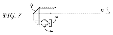
[0033]図7は、別の例示的な実施例における結合構造の態様を示す概略的な断面図である。図示された結合構造は、ロッドレンズ46及び銀めっきされた傾斜した面を有する台形プリズム54を含む。台形プリズムの長い基礎面は対向する第1及び第2の端部領域を含む。長い基礎面の第1の端部領域は導光路32の端面にぴったりくっついてそろえられる。長い基礎面の第2の端部領域は、導光路の下に、導光路の下面のエッジと並行して、ロッドレンズとそろえられる。1つの実施例において、台形プリズムはアクリル又はポリカーボネートから形成されてもよい。1つの実施例において、ロッドレンズは導光路の下面のエッジにわたってもよい。他の実施例は、ロッドレンズ及び導光路の2つの対向する端面の各々に沿って方向づけられる台形プリズムを含んでもよい。さらに別の実施例において、結合構造は、銀めっきされない傾斜した面を有する台形プリズムを含んでもよい。
[0033] FIG. 7 is a schematic cross-sectional view illustrating aspects of a coupling structure in another exemplary embodiment. The illustrated coupling structure includes a
[0034]図8は、別の例示的な実施例における結合構造の態様を示す概略的な断面図である。図示された結合構造はロッドレンズ46を含む。ロッドレンズの軸は導光路32の水平の対称面にあり、導光路の端面と並列に方向づけられてもよい。1つの実施例において、ロッドレンズは、導光路の端面にわたってもよい。他の実施例は、導光路の2つの対向する端面の各々に沿って方向づけられたロッドレンズを含んでもよい。
[0034] FIG. 8 is a schematic cross-sectional view illustrating aspects of the coupling structure in another exemplary embodiment. The illustrated coupling structure includes a
[0035]図9は、別の例示的な実施例における結合構造の態様を示す概略的な断面図である。図示された結合構造はロッドレンズ46及びレンズ状アレイ56を含む。ロッドレンズは、導光路38の傾斜した端面の近く及びそれと平行に方向づけられてもよい。1つの実施例において、レンズ状アレイは膜に埋め込まれてもよく、それは導光路の傾斜した端面に接合される。他の実施例において、ロッドレンズは、一次元の合成の放物線の集光器(compound parabolic concentrator)(ID−CPC)で置き換えられてもよい。さらに他の実施例において、レンズ状アレイは、組み合わされた光パワーについてID−CPC収集器で補われてもよく、1つの実施例において、ID−CPCはロッドレンズとレンズ状アレイの両方に取って代わってもよい。
[0035] FIG. 9 is a schematic cross-sectional view illustrating aspects of a coupling structure in another exemplary embodiment. The illustrated coupling structure includes a
[0036]図9に示された結合構造は、くさび形の導光路38の傾斜した端面へ光を結合するためにとりわけ使用されてもよく、その結果、図面に示されるように、導光路へ結合された光が上面を介して出る。この構成において、上面を出る光の空間的な均一性は、傾斜した端面へ結合する光の角度の均一性と関連する。したがって、結合構造が入射角に応じて高度に均一な光入力を提供することが望ましい。図9の実施例において、これは、レンズ状アレイ56及び/又は制限された範囲及び角度にわたって高い角度均一性をもって光を投影するID−CPCを選択することにより達成される。さらに、ロッドレンズ46は、レンズ状アレイの出口コーンよりいくらか鋭い様々な角度にわたって光を集めるように選択されてもよい。
[0036] The coupling structure shown in FIG. 9 may be used inter alia to couple light to the inclined end face of the wedge-shaped
[0037]上記に記載された結合構造の実施例は、1次元のみに光パワーを有する収集光学素子(ロッドレンズ、プリズム、レンズ状アレイ、ID−CPC収集器及び回折格子)を含む。したがって、これらの収集光学素子は、1次元のみで視覚システムエミッター30から光を収集する。したがって、図4の平面図の例によって示されるように、それらは、エッジに配置された複数の視覚システムエミッターから光を集めるように、導光路の全エッジ長にわたってもよい。しかし、他の実施例において、結合構造は、例えば、ドームレンズ及び2D−CPC収集器など、二次元に光パワーを有する類似した収集光学素子を含んでもよい。そのような実施例において、結合構造は、対応する一連の視覚システムエミッターに結合され、導光路32にさらに結合れた、一連の収集光学素子を含んでもよい。そのような配置は図10の例によって示され、収集光学素子58は2D収集光学素子を含む。
[0037] Embodiments of the coupling structure described above include collection optics (rod lenses, prisms, lenticular arrays, ID-CPC collectors and diffraction gratings) that have optical power in only one dimension. Thus, these collection optics collect light from the
[0038]上で識別された様々な収集光学素子は導光路への改善された結合効率を提供し得るが、それらがすべての場合に必要ではないことに留意されたい。例えば、導光路32の端において結合する場合、高い結合効率は、収集光学素子の使用なしに、より高い角度広がりの結合された光により達成されてもよく、拡散光抽出層(下記参照)は、光がより低い発散で収集される場合と比較して、著しく拡散の少ない強度を提供しなければならない。これは、より多くの光がより大きな数の反射にさらされるからである。しかし、光が導光路の底部側から結合される構成において、光が著しく低い発散で集められない場合、結合損失がもたらされ得る。
[0038] Note that although the various collection optics identified above may provide improved coupling efficiency to the light guide, they are not necessary in all cases. For example, when coupling at the end of the
[0039]ここで図9に戻ると、くさび形の導光路38は、実質的に平面の対向する上面及び下面を含む。上面及び下面は、いくつかの例において、0度と1度との間であってもよいくさび角を定義する。等しくない高さの対向する第1及び第2の端面は、上面及び下面に隣接して配置される。図9に示されるように、視覚システムエミッター30からの赤外光は、結合構造を介して導光路に入り、TIRによって導光路を伝播する。光は第1の端面から第2の端面に向かって導かれ、臨界前の(subcritical)入射角で上面又は下面に達し、実質的に平行にされた導光路の上面から屈折させられる。
[0039] Returning now to FIG. 9, the wedge-shaped
[0040]図9に示された実施例において、対向する上面又は下面に関する結合された光の入射角は、各反射の際にくさびの半分の角度の2倍だけ低減される。その結果、光が入る端面における入射角は光が漏れる上面又は下面に沿った位置にマッピングされることになる。TIR条件に反する光のみが導光路を出るので、導光路から投影されるすべての光は、通常、導光路媒体の屈折率、導波路を囲む媒体(例えば、空気)の屈折率、入射端面における光の角度、並びに、より高次において、くさびの厚さ及びくさび結合面における入射光の垂直の位置によって決定されるような臨界角から数度以内の、高い角度で出る。したがって、光の大部分が比較的大きな出射角(exit angle)で導光路を出るように、これらのパラメーターが選択されてもよい。結像検出器26に入れることができる視覚システム照明器からの散乱光の量を最小化するので、大きな出射角を提供することは有利である。さらに、上述のように、大きな値のθで導光路の上面から漏れる光束の空間分布が、導光路へ結合する光束の角度分布によって制御されることを示すことができる。
[0040] In the embodiment shown in FIG. 9, the angle of incidence of the combined light with respect to the opposing top or bottom surface is reduced by twice the half angle of the wedge during each reflection. As a result, the incident angle at the end surface where light enters is mapped to a position along the upper surface or the lower surface where light leaks. Since only light that violates the TIR condition exits the light guide, all light projected from the light guide typically has a refractive index of the light guide medium, a refractive index of the medium surrounding the waveguide (eg, air), and an incident end face. It exits at higher angles, within a few degrees from the critical angle, as determined by the angle of the light and, at higher orders, the thickness of the wedge and the vertical position of the incident light at the wedge coupling surface. Accordingly, these parameters may be selected so that the majority of the light exits the light guide with a relatively large exit angle. Providing a large exit angle is advantageous because it minimizes the amount of scattered light from the vision system illuminator that can enter the
[0041]図11は、別の例示的な実施例における光学系の態様を示す概略的な断面図である。図8に示されるように、光学系60は、シート状の導光路36及び結合構造34を含む。図11に示された実施例において、導光路は、ショットガラス社の製品である約3ミリメートルの厚さのB270ガラスのシートを含んでもよい。この製品は、850ナノメートルにおいて1メーターの経路長あたり54〜50パーセントの透過率を有する。
[0041] FIG. 11 is a schematic cross-sectional view illustrating aspects of an optical system in another exemplary embodiment. As shown in FIG. 8, the optical system 60 includes a sheet-like
[0042]導光路36は、実質的に平面で対向する上面及び下面、並びに当該上面及び下面に隣接する、実質的に等しい高さの対向する第1及び第2の端面を含む。視覚システムエミッター30からの赤外光は第1の端面から第2の端面に向かって導かれる;対向する面からの反射によって、導光路へ結合される赤外光は、TIRによって導光路を通じて伝播する。さらに以下に記載されるように、TIR条件は様々な方法で破綻して(すなわち、妨げられ)、上面及び下面において様々なモードの接触及び/又は物体検出につながってもよい。
[0042] The
[0043]例えば、導光路36又は導光路が光学的に結合される保護層44の上面上の指を利用することは、TIR条件を妨げて、光が導光路から逃げて指に反射することを可能にする。次いで反射された光は面の法線に関して比較的小さな角度で導光路を介して後方に伝播してもよく、結像検出器26によって結像されてもよい。さらに、反射された光束が指と導光路の上面との間の接触領域に依存するので、結像検出器に動作可能にリンクされたコンピューターは、1つ以上の物体と表示面との間の増加する又は減少する接触領域に対して応答するように構成されてもよい。このように、コンピューターは、接触イベント及び/又は継続して加えられる圧力に応答して、表面に与えられた圧力を検出し、ボリュームを上げたり写真上でズームインしたりするなど、適切な動作をとってもよい。
[0043] For example, utilizing a finger on the top surface of the
[0044]上述の接触検知のモードは、接触する物体によって光学的に「湿らせられている」導光路の面に依存する。しかし、多くの物体は、それらの材料特性又はトポロジーのため、それらが接触して配置される表面を確実には湿らせない。さらに、視覚システムが、表示面の近くにあるが接触していない物体を検知することができることが望まれてもよい。したがって、物体検知のより一般化されたモードが構想され、それは上述の接触検知の代わりに又はそれに加えて実行されてもよい。以下にさらに記載されるように、TIR条件は、検出される物体からの接触がないときは、制御された程度に妨げられてもよい。したがって、本明細書において記載された光学系は、接触検知ベースの表示面の検知及び追跡のほか、視覚ベースの表示面の検知及び追跡を可能にするように構成されてもよい。 [0044] The mode of touch detection described above depends on the surface of the light guide that is optically "moistened" by the contacting object. However, many objects do not reliably wet the surface on which they are placed because of their material properties or topology. Furthermore, it may be desirable for the vision system to be able to detect objects that are close to the display surface but not in contact. Thus, a more generalized mode of object detection is envisioned, which may be performed instead of or in addition to the touch detection described above. As described further below, TIR conditions may be disturbed to a controlled extent when there is no contact from the detected object. Accordingly, the optical system described herein may be configured to allow detection and tracking of a vision-based display surface as well as detection and tracking of a touch-sensitive display surface.
[0045]したがって、光学系60において、拡散層62は、導光路36の上面において、上面及び下面と平行して配置される。拡散層は、導光路の上面とその上の層、図示された実施例における保護層44、との間の界面において部分的にTIRを妨げる。拡散層とインタラクトすることにより、TIRによって他の方法で導光路を通じて導かれるいくらかの光は、臨界超過の入射角を得て、それは、その光が導光路から漏れることを可能にする。漏れる光は、TIRが妨げられる界面に関して上方又は下方へ移動してもよい。上方へ移動する光は、表示面12上又は表示面の近くに配置された1つ以上の物体16を照らしてもよい。
Accordingly, in the optical system 60, the
[0046]拡散層62が下面又は上面のいずれに配置されても、TIRの妨げ(フラストレーション)及び導光路36からの光の上方への漏れが生じ得る。拡散層が導光路の下面上に配置される実施例において、介在するエアギャップ又は他の低屈折率層は、光学的に導光路を分離して下の層への光結合の損失を防ぐため、TIR条件が適度に小さな入射角を介して広がることを保証するために使用されてもよい。表示コントラストを低下させる弱い拡散効果が表示層からの拡散部の距離の低減とともに減少するので、導光路の下面上に拡散層を配置することによって、可視表示光に対してコントラスト損失が低減されるという利点がもたらされる。さらに、導光路の下面に配置された表面レリーフ(surface-relief)型の拡散層を使用する場合、1つの顕著な利点は、漏れる光における方向の偏り(directional bias)である。具体的には、上面に向かって漏れる光束は、反対方向に漏れる光束に比べて20〜30パーセントだけ大きくなり得る。このように、漏れる光は、より効率的に、表示面12上の物体を照らすことができる。
[0046] Regardless of whether the
[0047]1つの実施例において、拡散層62は、導光路36上又は導光路内の三次元ボリュームにおいて複数の光拡散特性が分散される、ボリューム型(volume-type)の拡散層を含んでもよい。一つの例において、ボリューム型の拡散層は、分散されて固定される粒子などの、制御された密度の光散乱中心を有する軟質(柔軟な)フィルムを含んでもよい。軟質フィルムは、屈折率が一致した(index-matched)接着剤によって、又は任意の他の適切な方法で、導光路の上面又は下面に接合されてもよい。1つの例示的なボリューム型拡散フィルム層は、フュージョンオプティクス株式会社の製品ADF0505である。
[0047] In one embodiment, the diffusing
[0048]導光路36の上面に配置される時、ボリューム型の拡散層62は特定の利点を有する。ボリューム型の拡散層がこのように配置される場合、導光路は介在するエアギャップなしで上の層に直接取り付けられてもよい。エアギャップを省略することは、拡散特性が光学的濡れ(optical wetting)によって低減され得る表面レリーフ型(以下参照)の拡散層にとって有利ではないかもしれない。エアギャップの除去はエンジニアリングの見地から有用である;さらに、それは、階層構造における周囲光のフレネル反射によって引き起こされる特定の光学的アーティファクトを低減し得る。しかし、下面と、拡散層が導光路の最上面に直接積層されるとしても、LCD制御層22の上側に積層され得る適度な拡散部(図11に示されない)との間にエアギャップがなお使用されてもよいことに留意されたい。この場合、光学系の様々なエア・インターフェース(空気界面)のうちのいずれかにおける反射防止膜は、周囲光の反射によりコントラストの損失を減少させるのを支援するために使用されてもよい。
[0048] When placed on the upper surface of the
[0049]別の実施例において、拡散層62は、導光路36上又は導光路内の二次元表面上に複数の光拡散機構(光拡散機能、light-diffusing features)が配置される表面レリーフ型の拡散層を含んでもよい。例えば、拡散層は、凹面及び凸面の小型レンズ、くぼみ又は突起の周期的又は非周期的なアレイを含んでもよい。これらは、漏れる光の正確な制御を提供する、抽出機構として使用することができる。1つの実施例において、表面特性は、導光路上に直接成形されてもよい。適切な成形技術は、例として、熱成形及びuv一体成形を含む。別の実施例において、そのような特徴があるフィルムは、導光路の面上に積層されてもよいし、(例えば、熱プレス圧延によって)その上で広げられてもよいし、スクリーン印刷によって形成されてもよい。スクリーン印刷は、特に、低い先行投資コストのほか低い生産量コストを提供することができる例示的な選択肢である。そのような場合、いくつかの拡散技術に関連付けられる問題のある設備を一新するコストを回避することができる。さらに、スクリーン印刷方法、圧延方法及び類似した方法は、代替的な方法によって要求される積層の数を1つ減らし得る。圧延又はスクリーン印刷により適用することができる表面特性は、ホワイトTIR−回避(white TIR-frustrating)ドット、マイクロドット又は拡散パッドを含む。他の実施例において、ドット、マイクロドット又は拡散パッドは、導光路内に埋め込まれた二色性コーティングを施した表面レリーフなど、明らかに透明だが赤外反射性のものであってもよい。
[0049] In another embodiment, the
[0050]反射防止膜で覆われる場合、下面上に配置された拡散層は、周囲光を拡散する傾向がより少なくなって、全体のクリーナー及びより乳状でない外観を有する表示面を提供してもよい。このコンテキストにおいて、任意の拡散層が表示面の前に置かれる場合に、表示コントラストが低減され得ることが理解される。所与の拡散部がさらに表示面から遠ざけて平面に配置されるにつれて、表示コントラスト損失は増加し得る。また、所与の分離距離について、表示コントラスト損失は拡散層の拡散強度が増加するにつれて増加する。周囲光の反射によるコントラスト損失を低減するのに役立つように、拡散器を介して表示層を見ることにより引き起こされる直接的な画像の劣化とは対照的に、反射防止コーティングは、エアギャップの両側−(導光路の下面上に積層又は成形された)拡散部の下面、及び表示の最上面に配置又は積層された適度な拡散部の上面−に適用されてもよい。導光路の下面に配置された表面レリーフ型拡散部を使用する場合、1つの顕著な利点は、最下段の方へ漏れる光エネルギーと比較して、30%も、上方への散乱光に方向の偏りがあることを含み、したがって、表示面12上又は表示面の近くの物体に向かって投影される光の使用の効率を増加させる。 [0050] When covered with an anti-reflective coating, the diffuser layer disposed on the lower surface is less prone to diffuse ambient light and may provide a display surface having an overall cleaner and less milky appearance. Good. In this context, it is understood that the display contrast can be reduced if any diffusion layer is placed in front of the display surface. As a given diffuser is further placed in a plane away from the display surface, the display contrast loss can increase. Also, for a given separation distance, the display contrast loss increases as the diffusion intensity of the diffusion layer increases. In contrast to direct image degradation caused by looking at the display layer through a diffuser, the anti-reflective coating is applied to both sides of the air gap to help reduce contrast loss due to ambient light reflections. -It may be applied to the lower surface of the diffusion part (laminated or molded on the lower surface of the light guide) and the upper surface of an appropriate diffusion part arranged or laminated on the uppermost surface of the display. When using a surface relief diffuser located on the lower surface of the light guide, one significant advantage is that as much as 30% of the upward scattered light is directed to the light energy leaking towards the bottom. Including biasing, thus increasing the efficiency of the use of light projected onto an object on or near the display surface 12.
[0051]ボリューム型及び表面レリーフ型の拡散層からの光の拡散は、数学的に記述することができる。そのような拡散をモデル化する場合、方向余弦空間において回転対称であって拡散強度σによって決定される幅を有するガウス分布によって、実質的に平面の拡散層の特徴を表すことが便利である。したがって、所望の目標σは、以下に述べられるような予期された要求される正常な透過分布プロフィールと関連してもよい。 [0051] The diffusion of light from volume and surface relief type diffusion layers can be described mathematically. When modeling such diffusion, it is convenient to represent the characteristics of a substantially planar diffusion layer by a Gaussian distribution that is rotationally symmetric in the direction cosine space and has a width determined by the diffusion intensity σ. Thus, the desired target σ may be associated with an expected required normal transmission distribution profile as described below.
[0052]ボリューム型の拡散層について、n個の等しいガウス分布の畳み込みは、 [0052] For a volume-type diffusion layer, the convolution of n equal Gaussian distributions is
![]()
![]()
をもたらし、ここでθiは各層の角散乱プロフィールの半値全幅(FWHM)であり、θはすべての拡散層が等しいという仮定の下での同じ角度幅を表し、θeffは等しい拡散プロフィールを有するn個の隣接層についての結果として生じる有効角散乱プロフィールである。拡散媒体の内部で、光路は表面の法線に対して、ファクターcpだけ増加され、ここで Where θ i is the full width at half maximum (FWHM) of the angular scattering profile of each layer, θ represents the same angular width under the assumption that all diffusion layers are equal, and θ eff has the same diffusion profile The resulting effective angular scattering profile for n adjacent layers. Inside the diffusing medium, the optical path is increased by a factor c p relative to the surface normal, where
![]()
![]()
であり、θavgはn個のガウス分布の平均である。ボリューム型拡散層について、光路は2倍になり、したがって、 And θ avg is the average of n Gaussian distributions. For volume type diffusion layers, the optical path is doubled, so
![]()
![]()
及び、また And also

である。任意の適切な光線追跡(レイトレース)ユーティリィティによってモデル化する場合、角拡散はσによって定義される幅を有するガウス分布の観点から定義される。そのような場合、σは次の関係を使用して、有効FWHMの角度幅へと変換することができる: It is. When modeled with any suitable ray tracing utility, angular diffusion is defined in terms of a Gaussian distribution with a width defined by σ. In such cases, σ can be converted to an effective FWHM angular width using the following relationship:
![]()
![]()
また、空気中の対応する有効角度幅は次のように推定することができる Also, the corresponding effective angle width in the air can be estimated as follows.
したがって、ボリューム型拡散層の空気中の所望の正常な出口(exit)プロフィールは、 Therefore, the desired normal exit profile in the air of the volumetric diffusion layer is
である。
そのような方法で、導光路の出口面にわたる所与の出力均一性を達成するための目標の拡散特性(σによって定義される)は、所与の導光路の厚さ、相互作用長、材料吸収損失、及び結合される光の指示及び発散について計算されてもよい。いくつかの拡散部が正常な入射及び空気における角散乱プロフィールについて特徴づけられるので、その後、結果として生じるσは、適切な拡散層を選択するために、より物理的な設計基準(design metric)へと変換されてもよい。最後に、上記の分析はガウス分布に対応するものでるので、ガウス分布からの角散乱プロフィールの大きなずれ(departure)は、上記のモデル化において使用される有効角度幅に影響を及ぼし得る。そのような場合、ボリューム型拡散層として、プロフィールは、Henyey−Greensteinプロフィールによってより適切に記述され、プロフィール内のエネルギーの半分がプロフィールのFWHMをわずかに超える角度幅内に存在し従ってエネルギー分布に基づいて追加のファクターを要求するように、プロフィールを示してもよい。しかし、目標σがモデル最適化によって一旦決定されると、上に記載されるようなシグマ値のそのような返還は、正常な入射及び空気中において拡散層に要求される拡散特性についての適度に近接した記述を提供してもよく、その結果、適切な拡散層が導光路について選択されてもよいと考えられる。
It is.
In such a way, the target diffusion characteristic (defined by σ) to achieve a given output uniformity across the exit face of the light guide is given by the thickness, interaction length, material of the given light guide It may be calculated for the absorption loss and the indication and divergence of the coupled light. Since several diffusers are characterized for normal incidence and angular scattering profiles in air, the resulting σ is then transferred to a more physical design metric to select the appropriate diffuser layer. May be converted. Finally, since the above analysis corresponds to a Gaussian distribution, a large departure of the angular scattering profile from the Gaussian distribution can affect the effective angular width used in the above modeling. In such a case, as a volumetric diffusion layer, the profile is better described by a Henryy-Greenstein profile, where half of the energy in the profile is within an angular width slightly exceeding the FWHM of the profile and is therefore based on the energy distribution The profile may be shown to require additional factors. However, once the target σ is determined by model optimization, such a return of the sigma value as described above is reasonable for normal diffusion and diffusion characteristics required for the diffusion layer in air. It is contemplated that a close description may be provided so that an appropriate diffusion layer may be selected for the light guide.
同様に、表面レリーフ拡散層について、 Similarly, for the surface relief diffusion layer,
![]()
![]()
である。
媒体内部のモデルについて、測定された半値全幅を使用して、平均の角度において、
It is.
For the model inside the medium, using the measured full width at half maximum, at the average angle,
![]()
![]()
である。
ここで、正常な入射における予期される透過応答が決定される、
It is.
Where the expected transmission response at normal incidence is determined,
![]()
![]()
最後に、次の関係が得られる: Finally, the following relationship is obtained:
![]()
![]()
[0053]上記の理論の適用は、本発明において考えられる様々な実施例における、σの適切な値の、拡散層62についての意味のある角散乱プロフィール幅への転換のためのガイダンスを提供する。一例において、図3に示す結合構造の実施例により、導光路からの均一な照明を提供するためのσの計算された最適値は、コーナープリズムの内角に強く依存し、その値は、60度の内角の隣接したロッドレンズ46についての0.035から75度の内角についての0.06へと変化する。
[0053] Application of the above theory provides guidance for the conversion of an appropriate value of σ to a meaningful angular scattering profile width for the
[0054]導光路の出口面における均一性分布に影響を及ぼす追加のパラメーターは、導光路の厚さt、拡散部相互作用領域の長さL、視覚システムエミッター波長における材料吸収、及び導光路へ結合される光の角度分布を含む。予期され得るように、光の抽出の割合は、光導管(light-conduit)/拡散層界面における反射の数が増加するとともに、所与の距離にわたって増加する。そのため、より厚い導光路と比較して、より薄い導光路は、所与の距離にわたってより多くの反射を示し、したがって、それほど強い拡散層を必要としない。同様の理由から、より長い領域Lにわたる相互作用はより強くない拡散層を必要とする。さらに、材料吸収による減衰は所与の距離にわたって増加した割合で光損失を引き起こし、したがって、均一性を維持するために、それほど強くない拡散層を必要とする。導光路へ結合された光の角度の内容は、所与の厚さについて光が経験する反射の数に影響を与え、したがって、拡散層が導光路の下面に結合される実施例において、より弱い拡散器の必要性を指示する。そのため、出口面における均一性を維持するために、より少ない拡散能力がより高い入力角度に対して必要とされる。 [0054] Additional parameters that affect the uniformity distribution at the exit face of the light guide are the thickness t of the light guide, the length L of the diffuser interaction region, the material absorption at the vision system emitter wavelength, and to the light guide. Contains the angular distribution of the combined light. As can be expected, the rate of light extraction increases over a given distance as the number of reflections at the light-conduit / diffusion layer interface increases. Thus, as compared to a thicker light guide, a thinner light guide shows more reflection over a given distance and therefore does not require a much stronger diffusion layer. For similar reasons, interactions over longer regions L require less intense diffusion layers. Furthermore, attenuation due to material absorption causes light loss at an increased rate over a given distance, thus requiring a less strong diffusion layer to maintain uniformity. The angle content of the light coupled to the light guide affects the number of reflections that the light experiences for a given thickness, and thus is weaker in embodiments where the diffusing layer is coupled to the lower surface of the light guide. Direct the need for diffusers. Therefore, less diffusion capacity is required for higher input angles to maintain uniformity at the exit surface.
[0055]1つの実施例において、拡散層62は、結合構造中の1つ以上の収集光学素子から−例えば図11のロッドレンズ46から−の距離に応じて一様に拡散してもよい。それは、くぼみ、ドット、小型レンズなどが同様のサイズ、焦点特性及び/又は拡散能力であり、均一に間隔を空けられた、均一に形成されたボリューム型拡散層又は表面レリーフ型拡散層を含んでもよい。そのような実施例において、導光路36の上面を漏れる光束は、結合構造の近くで最大になり、結合構造からの距離が増加するにつれて指数関数的に減衰する。
[0055] In one embodiment, the diffusing
[0056]そのような拡散層が使用され、光が導光路36の単一の端面へ結合される実施例において、照明は、光が受け取られる導光路の端部に向かってより強くなってもよい。そのような拡散層が使用されるが、光が導光路の2つの対向する端面へ結合される実施例において、結果として生じる照明は、より均一であってもよいし、いくつかの用途にとっては十分に均一かもしれない。
[0056] In embodiments where such a diffusion layer is used and light is coupled to a single end face of the
[0057]しかし、さらに大きな均一性の照明を提供するために、拡散層の光拡散強度σが結合構造からの距離に応じて変化する実施例が考えられる。例えば、光拡散強度は結合構造からの距離が増加するにつれて増加してもよい;拡散層は結合構造の最も近くで拡散が最小となってもよく、結合構造からの距離が増加するにつれてより拡散しやすくなってもよい。この種の段階的な拡散層は、結合構造からの距離が増加するにつれて拡散中心の密度が増加する不均一に形成されたボリューム型拡散層を含んでもよいし、又は、結合構造からの距離が増加するにつれて、くぼみ、ドット、小型レンズなどが一連の増加するサイズ、増加する拡散能力又は減少するピッチで配列される、表面レリーフ型拡散層を含んでもよい。導光路の対向する端部へ光が結合される実施例において、拡散層の光拡散強度は、対向する端部の最も近くでより弱くなってもよく、導光路の中間部分においてより強くなってもよい。ある場合には、導光路の出口面にわたって高い均一性を達成するのに必要な拡散強度における変化は、実質的にガウス分布の形状であって、ゼロでないバイアスを有してもよい。 [0057] However, in order to provide even more uniform illumination, an embodiment is conceivable in which the light diffusion intensity σ of the diffusion layer varies with distance from the coupling structure. For example, the light diffusion intensity may increase as the distance from the bonded structure increases; the diffusion layer may be closest to the bonded structure and have minimal diffusion and become more diffuse as the distance from the bonded structure increases. It may be easier to do. This type of graded diffusion layer may include a non-uniform volume diffusion layer in which the density of diffusion centers increases as the distance from the bonded structure increases, or the distance from the bonded structure increases. As it increases, it may include a surface relief diffusion layer in which the depressions, dots, lenslets, etc. are arranged in a series of increasing sizes, increasing diffusing capacity or decreasing pitch. In embodiments where light is coupled to the opposite ends of the light guide, the light diffusing intensity of the diffusing layer may be weaker closest to the opposite ends and stronger at the middle portion of the light guide. Also good. In some cases, the change in diffusion intensity required to achieve high uniformity across the exit face of the light guide may be substantially Gaussian in shape and have a non-zero bias.
[0058]結合構造からの距離に応じて拡散層62の光拡散強度が変化する実施例において、変化は連続的であってもよく、拡散中心密度、表面レリーフ機構の特性などの連続的な変化に起因する。他の実施例において、光拡散強度の変化は離散的なステップで実現されてもよく、これらの特性の段階的な変化に起因する。例として、図12は、下面に段階的な可変の拡散層が適用される導光路についての放射照度データのグラフを示す。この例において、拡散層は、光が導光路へ結合される、導光路の対向する端面と平行に並べられた等しい幅の10個のストライプ形状のゾーンを含む。ここで、ストライプ形状のゾーンの光拡散強度σは、導光路の1つの端から中間まで、0.075、0.076、0.088、0.110、0.140と連続して増加し、次いで他方の端へと0.140、0.110、0.088、0.076及び0.075と連続して減少する。図12のグラフでは、導光路から投影された光の相対強度は垂直軸上にプロットされ、導光路にわたる拡散ゾーンの観点からの距離は水平軸上にプロットされる。平均強度は導光路にわたってかなり一定であるが、ゾーン間の移行に関連付けられる強度のくぼみが見られることに留意されたい。拡散強度が段階的なものとは対照的に導光路にわたって連続的な形で変化する場合、導光路にわたる出力の均一性はさらに改善され得る。
[0058] In embodiments in which the light diffusion intensity of the
[0059]ここで図11に戻ると、拡散層62は、一般に、同程度の上向き及び下向きの光束で、光を導光路36から漏れさせる。撮像(結像)検出器に達する下方へ散乱された光による大きなコントラスト損失を回避するために、漏れる光の出射角が十分に大きく、撮像検出器26の視野が十分に小さくてもよいが、再利用するためのなんらかの手段がない限り、そのような光は浪費されるままである。したがって、いくつかの実施例においては、導光路は、拡散層に対して平行に及び拡散層の表示面とは反対側に配置された、反射及び透過フィルター層を含んでもよい。当該フィルター層は、より低い入射角の光に対するよりも、大きな入射角の光に対して、反射が大きく透過が小さくてもよい。さらに、フィルター層は、可視光に対するよりも赤外光に対して反射が大きく透過が小さくてもよい。
[0059] Returning now to FIG. 11, the
[0060]したがって、図11に示された実施例は、導光路36の下面に配置されたフィルター層64を含む。上述のように、フィルター層は波長選択的な透過率及び反射率を示すように構成されてもよい。特に、フィルター層は、例えば、1つ以上の可視の波長帯域において実質的に透過し、比較的小さな入射角の入射光に対するよりも、比較的大きな入射角の入射光に対して、反射がずっと大きくてもよい。そのような特性は、2つの範囲の入射角に対する波長に応じて反射率Rがプロットされる図13の例によって示される。導光路の下面に適用されると、フィルター層は、そうでなければ導光路の下面から漏れて表示面12上の物体16の照明には使用不能であろう下方に拡散された光の向きを変えることにより、物体照明の効率を50〜100パーセント増加させ得る。
Thus, the embodiment shown in FIG. 11 includes a filter layer 64 disposed on the lower surface of the
[0061]フィルター層64は干渉コーティングを含んでもよい。1つの実施例において、フィルター層は、屈折率が制御された複数の薄い(10〜100ナノメートル)層が互いに積み重ねられた、ダイクロイック(二色性)フィルターの構造を有してもよい。別の実施例において、フィルター層は、材料の屈折率が制御された方法で連続的に変化する、ルゲート(rugate)フィルターの構造を有してもよい。1つの実施例において、フィルター層は、それが適用される導光路界面(インターフェース)において位相整合を示すように設計されてもよく、その結果、フレネル反射が最小化される。この場合、導光路36は、積層界面においてTIR条件を維持しつつ、別の基板上に積層されてもよい。フィルター層を積層と組み合わせることによって、視覚システム照明器の効率を増加させつつ、ハイコントラストな表示画像を提供することが可能となる。さらに、積層は、層状の光学系の剛性(rigidity)を増加させて、全体的により薄い設計を可能にし、それによって視覚システムの忠実度を改善することができる。
[0061] The filter layer 64 may include an interference coating. In one embodiment, the filter layer may have a dichroic filter structure in which a plurality of thin (10-100 nanometer) layers with controlled refractive index are stacked on top of each other. In another embodiment, the filter layer may have a rugate filter structure in which the refractive index of the material continuously changes in a controlled manner. In one embodiment, the filter layer may be designed to exhibit phase matching at the light guide interface (interface) to which it is applied, so that Fresnel reflection is minimized. In this case, the
[0062]図14は、別の例示的な実施例における光学系の態様を示す概略的な断面図である。光学系66において、シート状の導光路36自体が保護層として機能する。この実施例において、導光路はLCD制御層22より上に配置される。表示面12上又は表示面の近くの物体の効率的な照明のために、表面レリーフ型拡散層62が導光路の下面に配置され、導光路を光学的に分離するために薄いエアギャップが提供される。
[0062] FIG. 14 is a schematic cross-sectional view illustrating aspects of an optical system in another exemplary embodiment. In the
[0063]続いて図14において、適度な拡散層44がLCD制御層22の最上面に積層され、視覚システムが、実質的に上述されるように、LCD制御層より下に配置される。各々が他の実施例のコンテキストにおいて上に記載される少なくとも3つの設計態様を考慮して、図14に示された構成は、表示面12上又は表示面の近くに配置された物体の非常に効率的な照明を提供する。第1に、LCD制御層は導光路の照明路の外部に配置され、投影された光の減衰を引き起こさない。第2に、表面レリーフ型拡散層62が導光路の下面に配置され、表示面に向かって照明を偏らせる。第3に、フィルター層64は拡散層より下に配置され、物体を照らすのに有用となるように、下方の方向に拡散する十分な量の光の向きを変えるように構成される。
[0063] Continuing in FIG. 14, a
[0064]最後に、本明細書において記載された項目、システム及び方法は本来例示的なものであり、多数の変更が考えられるので、これらの特定の実施例又は例は限定する意味で考えるべきでないことが理解される。したがって、本開示は、本明細書において開示された様々なシステム及び方法のすべての新規で非自明な組み合わせ及びサブコンビネーションのほかそれらのすべての等価物を含む。 [0064] Finally, since the items, systems and methods described herein are exemplary in nature and numerous modifications are possible, these specific examples or examples should be considered in a limiting sense. It is understood that it is not. Accordingly, this disclosure includes all novel and non-obvious combinations and subcombinations of the various systems and methods disclosed herein as well as all their equivalents.
Claims (11)
前記表示面の法線に対して狭い範囲の角度の赤外光を結像するように構成された結像検出器であって、前記結像される赤外光は前記表示面上又は前記表示面の近くに配置された1つ以上の物体からの反射を含む、結像検出器と、
前記1つ以上の物体を照らすために、前記赤外光を放射するように構成された視覚システムエミッターと、
対向する上面及び下面並びに対向する端面を有する可視光及び赤外光を伝達可能な導光路であって、前記導光路上又は前記導光路内に配置されて前記上面及び下面に平行なボリューム型の拡散層を有し、前記視覚システムエミッターからの前記赤外光を受信し、前記上面及び/又は下面からの全反射を介して1つの端面から対向する端面に向かって前記赤外光を導くとともに、前記ボリューム型の拡散層による全反射の妨げによって前記1つ以上の物体上へ前記赤外光を投影するように構成され、前記ボリューム型の拡散層は3次元に分散された複数の光拡散特性を含む、導光路と
を具備する統合された視覚及び表示システム。 A display image forming layer configured to transmit a display image for viewing through a display surface;
An imaging detector configured to image infrared light having a narrow range of angles with respect to a normal line of the display surface, wherein the formed infrared light is on the display surface or the display An imaging detector comprising reflections from one or more objects located near the surface;
A vision system emitter configured to emit the infrared light to illuminate the one or more objects;
A light guide that can transmit visible light and infrared light having opposite upper and lower surfaces and opposite end surfaces, and is disposed on or in the light guide and is parallel to the upper and lower surfaces. has a diffusion layer, wherein the receiving the infrared light from the vision system the emitter, the upper surface and / or through the total reflection from the lower surface toward the end surface facing the one end face rather guiding the infrared light In addition , the volume type diffusion layer is configured to project the infrared light onto the one or more objects by preventing total reflection by the volume type diffusion layer , and the volume type diffusion layer includes a plurality of light beams dispersed in three dimensions. An integrated vision and display system comprising a light guide with diffusing properties.
Applications Claiming Priority (5)
| Application Number | Priority Date | Filing Date | Title |
|---|---|---|---|
| US23596209P | 2009-08-21 | 2009-08-21 | |
| US61/235,962 | 2009-08-21 | ||
| US12/621,785 | 2009-11-19 | ||
| US12/621,785 US8730212B2 (en) | 2009-08-21 | 2009-11-19 | Illuminator for touch- and object-sensitive display |
| PCT/US2010/046141 WO2011022632A2 (en) | 2009-08-21 | 2010-08-20 | Illuminator for touch- and object-sensitive display |
Publications (3)
| Publication Number | Publication Date |
|---|---|
| JP2013502588A JP2013502588A (en) | 2013-01-24 |
| JP2013502588A5 JP2013502588A5 (en) | 2013-08-22 |
| JP5639174B2 true JP5639174B2 (en) | 2014-12-10 |
Family
ID=43604965
Family Applications (1)
| Application Number | Title | Priority Date | Filing Date |
|---|---|---|---|
| JP2012525724A Expired - Fee Related JP5639174B2 (en) | 2009-08-21 | 2010-08-20 | Integrated visual and display system |
Country Status (10)
| Country | Link |
|---|---|
| US (1) | US8730212B2 (en) |
| EP (1) | EP2467753B1 (en) |
| JP (1) | JP5639174B2 (en) |
| KR (1) | KR101691248B1 (en) |
| CN (1) | CN102472917A (en) |
| BR (1) | BR112012003867A2 (en) |
| CA (1) | CA2768070A1 (en) |
| MY (1) | MY159236A (en) |
| RU (1) | RU2532696C2 (en) |
| WO (1) | WO2011022632A2 (en) |
Families Citing this family (59)
| Publication number | Priority date | Publication date | Assignee | Title |
|---|---|---|---|---|
| US8553014B2 (en) | 2008-06-19 | 2013-10-08 | Neonode Inc. | Optical touch screen systems using total internal reflection |
| SE533704C2 (en) | 2008-12-05 | 2010-12-07 | Flatfrog Lab Ab | Touch sensitive apparatus and method for operating the same |
| US9158416B2 (en) | 2009-02-15 | 2015-10-13 | Neonode Inc. | Resilient light-based touch surface |
| EP2523081B1 (en) * | 2010-01-06 | 2019-09-18 | Huawei Device Co., Ltd. | Method and terminal for displaying picture/interface |
| KR101749266B1 (en) * | 2010-03-24 | 2017-07-04 | 삼성디스플레이 주식회사 | Touch sensing display device and cumputer-readable medium |
| US8674965B2 (en) * | 2010-11-18 | 2014-03-18 | Microsoft Corporation | Single camera display device detection |
| KR101942114B1 (en) * | 2011-02-02 | 2019-01-24 | 플라트프로그 라보라토리즈 에이비 | Optical incoupling for touch-sensitive systems |
| JP6053110B2 (en) * | 2011-07-07 | 2016-12-27 | 株式会社アルバック | Vacuum deposition equipment |
| CN103186289A (en) * | 2011-12-28 | 2013-07-03 | 富泰华工业(深圳)有限公司 | Touch control display device |
| US10030846B2 (en) | 2012-02-14 | 2018-07-24 | Svv Technology Innovations, Inc. | Face-lit waveguide illumination systems |
| US20130234990A1 (en) * | 2012-03-06 | 2013-09-12 | Smart Technologies Ulc | Interactive input system and method |
| US9024917B2 (en) * | 2012-03-13 | 2015-05-05 | Neonode Inc. | Side-light display illuminator |
| US10168835B2 (en) | 2012-05-23 | 2019-01-01 | Flatfrog Laboratories Ab | Spatial resolution in touch displays |
| US9857916B2 (en) * | 2012-07-24 | 2018-01-02 | Flatfrog Laboratories Ab | Optical coupling in touch-sensing systems using diffusively transmitting element |
| US9329726B2 (en) * | 2012-10-26 | 2016-05-03 | Qualcomm Incorporated | System and method for capturing editable handwriting on a display |
| US20150331545A1 (en) * | 2012-12-17 | 2015-11-19 | FlatFrog Laboraties AB | Laminated optical element for touch-sensing systems |
| WO2014098742A1 (en) * | 2012-12-17 | 2014-06-26 | Flatfrog Laboratories Ab | Edge-coupled touch-sensitive apparatus |
| US20150324028A1 (en) * | 2012-12-17 | 2015-11-12 | Flatfrog Laboratories Ab | Optical coupling of light into touch-sensing systems |
| US10019113B2 (en) | 2013-04-11 | 2018-07-10 | Flatfrog Laboratories Ab | Tomographic processing for touch detection |
| US9874978B2 (en) | 2013-07-12 | 2018-01-23 | Flatfrog Laboratories Ab | Partial detect mode |
| US10146376B2 (en) | 2014-01-16 | 2018-12-04 | Flatfrog Laboratories Ab | Light coupling in TIR-based optical touch systems |
| US10126882B2 (en) | 2014-01-16 | 2018-11-13 | Flatfrog Laboratories Ab | TIR-based optical touch systems of projection-type |
| TWI534686B (en) * | 2014-01-22 | 2016-05-21 | 廣達電腦股份有限公司 | Optical touch screen |
| GB201406550D0 (en) * | 2014-04-11 | 2014-05-28 | Lomas David G | Optical touch screen |
| US9614724B2 (en) | 2014-04-21 | 2017-04-04 | Microsoft Technology Licensing, Llc | Session-based device configuration |
| US20150309663A1 (en) * | 2014-04-28 | 2015-10-29 | Qualcomm Incorporated | Flexible air and surface multi-touch detection in mobile platform |
| US9430667B2 (en) | 2014-05-12 | 2016-08-30 | Microsoft Technology Licensing, Llc | Managed wireless distribution network |
| US9384334B2 (en) | 2014-05-12 | 2016-07-05 | Microsoft Technology Licensing, Llc | Content discovery in managed wireless distribution networks |
| US10111099B2 (en) | 2014-05-12 | 2018-10-23 | Microsoft Technology Licensing, Llc | Distributing content in managed wireless distribution networks |
| US9384335B2 (en) | 2014-05-12 | 2016-07-05 | Microsoft Technology Licensing, Llc | Content delivery prioritization in managed wireless distribution networks |
| US9874914B2 (en) | 2014-05-19 | 2018-01-23 | Microsoft Technology Licensing, Llc | Power management contracts for accessory devices |
| US10037202B2 (en) | 2014-06-03 | 2018-07-31 | Microsoft Technology Licensing, Llc | Techniques to isolating a portion of an online computing service |
| US9367490B2 (en) | 2014-06-13 | 2016-06-14 | Microsoft Technology Licensing, Llc | Reversible connector for accessory devices |
| EP3161594A4 (en) | 2014-06-27 | 2018-01-17 | FlatFrog Laboratories AB | Detection of surface contamination |
| US9720548B2 (en) | 2014-06-27 | 2017-08-01 | Microsoft Technology Licensing, Llc | See-through IR frontlight with embedded partially reflective facets |
| US9652082B1 (en) * | 2014-08-20 | 2017-05-16 | Amazon Technologies, Inc. | Space efficient electronic device component configurations |
| US11182023B2 (en) | 2015-01-28 | 2021-11-23 | Flatfrog Laboratories Ab | Dynamic touch quarantine frames |
| US10318074B2 (en) | 2015-01-30 | 2019-06-11 | Flatfrog Laboratories Ab | Touch-sensing OLED display with tilted emitters |
| EP3537269A1 (en) | 2015-02-09 | 2019-09-11 | FlatFrog Laboratories AB | Optical touch system |
| US10401546B2 (en) | 2015-03-02 | 2019-09-03 | Flatfrog Laboratories Ab | Optical component for light coupling |
| US10901548B2 (en) * | 2015-04-07 | 2021-01-26 | Omnivision Technologies, Inc. | Touch screen rear projection display |
| CN104793814A (en) * | 2015-05-12 | 2015-07-22 | 京东方科技集团股份有限公司 | Optical touch control device and touch control display device |
| US10775937B2 (en) | 2015-12-09 | 2020-09-15 | Flatfrog Laboratories Ab | Stylus identification |
| US11416041B2 (en) | 2016-05-23 | 2022-08-16 | Microsoft Technology Licensing, Llc. | Device having display integrated infrared and visible light source |
| WO2018096430A1 (en) | 2016-11-24 | 2018-05-31 | Flatfrog Laboratories Ab | Automatic optimisation of touch signal |
| KR102344055B1 (en) | 2016-12-07 | 2021-12-28 | 플라트프로그 라보라토리즈 에이비 | improved touch device |
| US10963104B2 (en) | 2017-02-06 | 2021-03-30 | Flatfrog Laboratories Ab | Optical coupling in touch-sensing systems |
| EP3602258B1 (en) | 2017-03-22 | 2024-05-08 | FlatFrog Laboratories AB | Pen differentiation for touch displays |
| EP3602259A4 (en) | 2017-03-28 | 2021-01-20 | FlatFrog Laboratories AB | Touch sensing apparatus and method for assembly |
| DE102017119983B3 (en) * | 2017-08-31 | 2018-09-27 | JENETRIC GmbH | Apparatus for contact-based simultaneous recording of autopod impressions |
| CN111052058B (en) | 2017-09-01 | 2023-10-20 | 平蛙实验室股份公司 | Improved optical component |
| US11481568B1 (en) | 2017-12-29 | 2022-10-25 | Cognex Corporation | Dome illuminator for vision system camera and method for using the same |
| US11567610B2 (en) | 2018-03-05 | 2023-01-31 | Flatfrog Laboratories Ab | Detection line broadening |
| US20190361569A1 (en) * | 2018-03-28 | 2019-11-28 | Ubi interactive inc. | Interactive screen devices, systems, and methods |
| US20210255662A1 (en) * | 2018-10-20 | 2021-08-19 | Flatfrog Laboratories Ab | Frame for a touch-sensitive device and tool therefor |
| CN109508119B (en) * | 2018-12-21 | 2020-06-30 | 武汉华星光电半导体显示技术有限公司 | Floating touch display device and floating touch method |
| US11943563B2 (en) | 2019-01-25 | 2024-03-26 | FlatFrog Laboratories, AB | Videoconferencing terminal and method of operating the same |
| WO2021162602A1 (en) | 2020-02-10 | 2021-08-19 | Flatfrog Laboratories Ab | Improved touch-sensing apparatus |
| WO2024074960A1 (en) * | 2022-10-04 | 2024-04-11 | 3M Innovative Properties Company | Display systems using multilayer optical films |
Family Cites Families (31)
| Publication number | Priority date | Publication date | Assignee | Title |
|---|---|---|---|---|
| US6002829A (en) | 1992-03-23 | 1999-12-14 | Minnesota Mining And Manufacturing Company | Luminaire device |
| JPH06130385A (en) | 1992-10-16 | 1994-05-13 | Mitsubishi Electric Corp | Surface light emitting device |
| JP3347302B2 (en) * | 1998-07-14 | 2002-11-20 | 株式会社日立製作所 | Liquid crystal display |
| TW523627B (en) * | 1998-07-14 | 2003-03-11 | Hitachi Ltd | Liquid crystal display device |
| JP3457591B2 (en) * | 1999-10-08 | 2003-10-20 | インターナショナル・ビジネス・マシーンズ・コーポレーション | Liquid crystal display |
| US6421104B1 (en) | 1999-10-22 | 2002-07-16 | Motorola, Inc. | Front illuminator for a liquid crystal display and method of making same |
| JP3774616B2 (en) | 2000-06-29 | 2006-05-17 | 株式会社日立製作所 | Lighting device and light guide plate manufacturing method |
| US6648485B1 (en) * | 2000-11-13 | 2003-11-18 | International Business Machines Corporation | Highly collimating tapered light guide for uniform illumination of flat panel displays |
| US6738051B2 (en) | 2001-04-06 | 2004-05-18 | 3M Innovative Properties Company | Frontlit illuminated touch panel |
| JP2002313121A (en) | 2001-04-16 | 2002-10-25 | Nitto Denko Corp | Luminaire with touch panel and reflective liquid crystal display device |
| JP2003015133A (en) * | 2001-04-27 | 2003-01-15 | Citizen Watch Co Ltd | Liquid crystal display device |
| JP2002369064A (en) | 2001-06-08 | 2002-12-20 | Toshiba Corp | Image pickup device and portable information terminal |
| US20030095401A1 (en) | 2001-11-20 | 2003-05-22 | Palm, Inc. | Non-visible light display illumination system and method |
| JP2007506178A (en) | 2003-09-22 | 2007-03-15 | コニンクリユケ フィリップス エレクトロニクス エヌ.ブイ. | Light touch screen |
| CN101174028B (en) * | 2004-03-29 | 2015-05-20 | 索尼株式会社 | Optical device and virtual image display device |
| JP4743846B2 (en) * | 2005-05-10 | 2011-08-10 | シチズン電子株式会社 | Optical communication apparatus and information equipment using the same |
| US8013845B2 (en) * | 2005-12-30 | 2011-09-06 | Flatfrog Laboratories Ab | Optical touch pad with multilayer waveguide |
| KR100673041B1 (en) * | 2006-05-16 | 2007-01-22 | 주식회사 세코닉스 | Display device for intercepting the external light |
| US7552402B2 (en) * | 2006-06-22 | 2009-06-23 | Microsoft Corporation | Interface orientation using shadows |
| US20080007541A1 (en) * | 2006-07-06 | 2008-01-10 | O-Pen A/S | Optical touchpad system and waveguide for use therein |
| US8022941B2 (en) * | 2006-10-12 | 2011-09-20 | Disney Enterprises, Inc. | Multi-user touch screen |
| US7548677B2 (en) * | 2006-10-12 | 2009-06-16 | Microsoft Corporation | Interactive display using planar radiation guide |
| JP4775247B2 (en) | 2006-12-21 | 2011-09-21 | 三菱電機株式会社 | Position detection device |
| WO2009020940A2 (en) | 2007-08-03 | 2009-02-12 | Perceptive Pixel, Inc. | Multi-touch sensing through frustrated total internal reflection |
| US8125458B2 (en) * | 2007-09-28 | 2012-02-28 | Microsoft Corporation | Detecting finger orientation on a touch-sensitive device |
| US8581852B2 (en) * | 2007-11-15 | 2013-11-12 | Microsoft Corporation | Fingertip detection for camera based multi-touch systems |
| KR101407300B1 (en) * | 2007-11-19 | 2014-06-13 | 엘지디스플레이 주식회사 | Multi touch flat display module |
| US7949213B2 (en) | 2007-12-07 | 2011-05-24 | Qualcomm Mems Technologies, Inc. | Light illumination of displays with front light guide and coupling elements |
| JP2009147553A (en) | 2007-12-12 | 2009-07-02 | Fujifilm Corp | Driving method for solid imaging element, and imaging device |
| US20090322706A1 (en) * | 2008-06-26 | 2009-12-31 | Symbol Technologies, Inc. | Information display with optical data capture |
| CN201247460Y (en) * | 2008-07-30 | 2009-05-27 | 青岛海信电器股份有限公司 | Display device |
-
2009
- 2009-11-19 US US12/621,785 patent/US8730212B2/en not_active Expired - Fee Related
-
2010
- 2010-08-20 JP JP2012525724A patent/JP5639174B2/en not_active Expired - Fee Related
- 2010-08-20 EP EP10810653.5A patent/EP2467753B1/en not_active Not-in-force
- 2010-08-20 WO PCT/US2010/046141 patent/WO2011022632A2/en active Application Filing
- 2010-08-20 CN CN2010800371196A patent/CN102472917A/en active Pending
- 2010-08-20 KR KR1020127004312A patent/KR101691248B1/en active IP Right Grant
- 2010-08-20 RU RU2012106118/28A patent/RU2532696C2/en not_active IP Right Cessation
- 2010-08-20 MY MYPI2012000278A patent/MY159236A/en unknown
- 2010-08-20 BR BR112012003867A patent/BR112012003867A2/en not_active Application Discontinuation
- 2010-08-20 CA CA2768070A patent/CA2768070A1/en not_active Abandoned
Also Published As
| Publication number | Publication date |
|---|---|
| JP2013502588A (en) | 2013-01-24 |
| EP2467753A4 (en) | 2014-07-16 |
| RU2012106118A (en) | 2013-08-27 |
| BR112012003867A2 (en) | 2016-03-29 |
| KR20120057618A (en) | 2012-06-05 |
| US8730212B2 (en) | 2014-05-20 |
| RU2532696C2 (en) | 2014-11-10 |
| EP2467753A2 (en) | 2012-06-27 |
| CA2768070A1 (en) | 2011-02-24 |
| KR101691248B1 (en) | 2016-12-29 |
| MY159236A (en) | 2016-12-30 |
| EP2467753B1 (en) | 2016-11-09 |
| US20110043490A1 (en) | 2011-02-24 |
| WO2011022632A3 (en) | 2011-07-21 |
| CN102472917A (en) | 2012-05-23 |
| WO2011022632A2 (en) | 2011-02-24 |
Similar Documents
| Publication | Publication Date | Title |
|---|---|---|
| JP5639174B2 (en) | Integrated visual and display system | |
| US8619062B2 (en) | Touch-pressure sensing in a display panel | |
| US8218237B2 (en) | Rear-projection display | |
| US8358901B2 (en) | Optic having a cladding | |
| US9535537B2 (en) | Hover detection in an interactive display device | |
| TWI609334B (en) | Fingerprint image capturing device | |
| US10515253B2 (en) | Optical fingerprint sensor | |
| TWI517054B (en) | Fingerprint image capturing device | |
| WO2017118031A1 (en) | Optical fingerprint sensor module | |
| JP2013502692A (en) | Concentrator for illumination optics | |
| JP2012528358A (en) | Fabrication of optical elements with cladding | |
| CN110088674B (en) | Backlight module, display device and electronic equipment | |
| WO2017118030A1 (en) | Optical fingerprint sensor module | |
| US20110241977A1 (en) | Enhanced viewing brightness for surface display | |
| WO2020181447A1 (en) | Optical film layer structure, backlight module, display apparatus and electronic device | |
| CN210573819U (en) | Backlight module, liquid crystal display device and electronic equipment | |
| CN210155480U (en) | Optical film layer structure, backlight module, liquid crystal display device and electronic equipment | |
| US8153977B2 (en) | Optic having a dichroic reflector | |
| KR102284460B1 (en) | Optical film for fingerprinting recognition | |
| KR102204164B1 (en) | Opotical film for fingerprinting | |
| CN210155479U (en) | Optical film layer structure, backlight module, liquid crystal display device and electronic equipment | |
| CN210155478U (en) | Optical film layer structure, backlight module, liquid crystal display device and electronic equipment | |
| CN210155477U (en) | Backlight module, liquid crystal display device and electronic equipment | |
| CN210402373U (en) | Sensing module | |
| CN210401944U (en) | Backlight module, display device and electronic equipment |
Legal Events
| Date | Code | Title | Description |
|---|---|---|---|
| A521 | Request for written amendment filed |
Free format text: JAPANESE INTERMEDIATE CODE: A523 Effective date: 20130704 |
|
| A621 | Written request for application examination |
Free format text: JAPANESE INTERMEDIATE CODE: A621 Effective date: 20130704 |
|
| A131 | Notification of reasons for refusal |
Free format text: JAPANESE INTERMEDIATE CODE: A131 Effective date: 20140527 |
|
| A521 | Request for written amendment filed |
Free format text: JAPANESE INTERMEDIATE CODE: A523 Effective date: 20140701 |
|
| TRDD | Decision of grant or rejection written | ||
| A01 | Written decision to grant a patent or to grant a registration (utility model) |
Free format text: JAPANESE INTERMEDIATE CODE: A01 Effective date: 20140924 |
|
| A61 | First payment of annual fees (during grant procedure) |
Free format text: JAPANESE INTERMEDIATE CODE: A61 Effective date: 20141023 |
|
| R150 | Certificate of patent or registration of utility model |
Ref document number: 5639174 Country of ref document: JP Free format text: JAPANESE INTERMEDIATE CODE: R150 |
|
| S111 | Request for change of ownership or part of ownership |
Free format text: JAPANESE INTERMEDIATE CODE: R313113 |
|
| R350 | Written notification of registration of transfer |
Free format text: JAPANESE INTERMEDIATE CODE: R350 |
|
| R250 | Receipt of annual fees |
Free format text: JAPANESE INTERMEDIATE CODE: R250 |
|
| R250 | Receipt of annual fees |
Free format text: JAPANESE INTERMEDIATE CODE: R250 |
|
| R250 | Receipt of annual fees |
Free format text: JAPANESE INTERMEDIATE CODE: R250 |
|
| R250 | Receipt of annual fees |
Free format text: JAPANESE INTERMEDIATE CODE: R250 |
|
| R250 | Receipt of annual fees |
Free format text: JAPANESE INTERMEDIATE CODE: R250 |
|
| LAPS | Cancellation because of no payment of annual fees |