JP5624463B2 - Memory cell using reversible resistance switching element by selective attachment and method of forming the same - Google Patents
Memory cell using reversible resistance switching element by selective attachment and method of forming the same Download PDFInfo
- Publication number
- JP5624463B2 JP5624463B2 JP2010514824A JP2010514824A JP5624463B2 JP 5624463 B2 JP5624463 B2 JP 5624463B2 JP 2010514824 A JP2010514824 A JP 2010514824A JP 2010514824 A JP2010514824 A JP 2010514824A JP 5624463 B2 JP5624463 B2 JP 5624463B2
- Authority
- JP
- Japan
- Prior art keywords
- forming
- layer
- switching element
- reversible resistance
- nickel
- Prior art date
- Legal status (The legal status is an assumption and is not a legal conclusion. Google has not performed a legal analysis and makes no representation as to the accuracy of the status listed.)
- Expired - Fee Related
Links
- 230000015654 memory Effects 0.000 title claims description 133
- 230000002441 reversible effect Effects 0.000 title claims description 100
- 238000000034 method Methods 0.000 title claims description 67
- PXHVJJICTQNCMI-UHFFFAOYSA-N Nickel Chemical compound [Ni] PXHVJJICTQNCMI-UHFFFAOYSA-N 0.000 claims description 80
- 229910052759 nickel Inorganic materials 0.000 claims description 40
- 239000000758 substrate Substances 0.000 claims description 32
- 230000008569 process Effects 0.000 claims description 27
- 238000000151 deposition Methods 0.000 claims description 26
- 238000005137 deposition process Methods 0.000 claims description 20
- -1 V 2 O 5 Inorganic materials 0.000 claims description 14
- 238000005530 etching Methods 0.000 claims description 13
- 238000009713 electroplating Methods 0.000 claims description 11
- 229910018072 Al 2 O 3 Inorganic materials 0.000 claims description 2
- 229910010413 TiO 2 Inorganic materials 0.000 claims description 2
- 239000010410 layer Substances 0.000 description 212
- 239000004020 conductor Substances 0.000 description 76
- 239000000463 material Substances 0.000 description 62
- XUIMIQQOPSSXEZ-UHFFFAOYSA-N Silicon Chemical compound [Si] XUIMIQQOPSSXEZ-UHFFFAOYSA-N 0.000 description 48
- 229910052710 silicon Inorganic materials 0.000 description 48
- 239000010703 silicon Substances 0.000 description 48
- 230000004888 barrier function Effects 0.000 description 47
- 229910000480 nickel oxide Inorganic materials 0.000 description 39
- GNRSAWUEBMWBQH-UHFFFAOYSA-N oxonickel Chemical compound [Ni]=O GNRSAWUEBMWBQH-UHFFFAOYSA-N 0.000 description 39
- 229910052751 metal Inorganic materials 0.000 description 28
- 239000002184 metal Substances 0.000 description 28
- 238000004519 manufacturing process Methods 0.000 description 21
- 229910052721 tungsten Inorganic materials 0.000 description 20
- 239000010937 tungsten Substances 0.000 description 20
- 239000012790 adhesive layer Substances 0.000 description 18
- 239000004065 semiconductor Substances 0.000 description 18
- 230000015572 biosynthetic process Effects 0.000 description 17
- 229910021332 silicide Inorganic materials 0.000 description 17
- FVBUAEGBCNSCDD-UHFFFAOYSA-N silicide(4-) Chemical compound [Si-4] FVBUAEGBCNSCDD-UHFFFAOYSA-N 0.000 description 17
- 229910021420 polycrystalline silicon Inorganic materials 0.000 description 13
- 229920005591 polysilicon Polymers 0.000 description 13
- 230000008021 deposition Effects 0.000 description 11
- 239000010936 titanium Substances 0.000 description 11
- VYPSYNLAJGMNEJ-UHFFFAOYSA-N Silicium dioxide Chemical compound O=[Si]=O VYPSYNLAJGMNEJ-UHFFFAOYSA-N 0.000 description 10
- NRTOMJZYCJJWKI-UHFFFAOYSA-N Titanium nitride Chemical compound [Ti]#N NRTOMJZYCJJWKI-UHFFFAOYSA-N 0.000 description 10
- 239000003989 dielectric material Substances 0.000 description 10
- MZLGASXMSKOWSE-UHFFFAOYSA-N tantalum nitride Chemical compound [Ta]#N MZLGASXMSKOWSE-UHFFFAOYSA-N 0.000 description 10
- 229910052719 titanium Inorganic materials 0.000 description 10
- WFKWXMTUELFFGS-UHFFFAOYSA-N tungsten Chemical compound [W] WFKWXMTUELFFGS-UHFFFAOYSA-N 0.000 description 10
- 229910052715 tantalum Inorganic materials 0.000 description 9
- 239000010409 thin film Substances 0.000 description 9
- 238000000137 annealing Methods 0.000 description 8
- ORQBXQOJMQIAOY-UHFFFAOYSA-N nobelium Chemical group [No] ORQBXQOJMQIAOY-UHFFFAOYSA-N 0.000 description 8
- 229910000990 Ni alloy Inorganic materials 0.000 description 7
- 229910000577 Silicon-germanium Inorganic materials 0.000 description 7
- LEVVHYCKPQWKOP-UHFFFAOYSA-N [Si].[Ge] Chemical compound [Si].[Ge] LEVVHYCKPQWKOP-UHFFFAOYSA-N 0.000 description 7
- 229910052782 aluminium Inorganic materials 0.000 description 7
- 239000007864 aqueous solution Substances 0.000 description 7
- ZGDWHDKHJKZZIQ-UHFFFAOYSA-N cobalt nickel Chemical compound [Co].[Ni].[Ni].[Ni] ZGDWHDKHJKZZIQ-UHFFFAOYSA-N 0.000 description 7
- 229910052758 niobium Inorganic materials 0.000 description 7
- 230000003647 oxidation Effects 0.000 description 7
- 238000007254 oxidation reaction Methods 0.000 description 7
- 229910052720 vanadium Inorganic materials 0.000 description 7
- 229910052732 germanium Inorganic materials 0.000 description 6
- GNPVGFCGXDBREM-UHFFFAOYSA-N germanium atom Chemical compound [Ge] GNPVGFCGXDBREM-UHFFFAOYSA-N 0.000 description 6
- 229910052581 Si3N4 Inorganic materials 0.000 description 5
- 229910045601 alloy Inorganic materials 0.000 description 5
- 239000000956 alloy Substances 0.000 description 5
- 238000005229 chemical vapour deposition Methods 0.000 description 5
- 235000012239 silicon dioxide Nutrition 0.000 description 5
- 239000000377 silicon dioxide Substances 0.000 description 5
- HQVNEWCFYHHQES-UHFFFAOYSA-N silicon nitride Chemical compound N12[Si]34N5[Si]62N3[Si]51N64 HQVNEWCFYHHQES-UHFFFAOYSA-N 0.000 description 5
- IJGRMHOSHXDMSA-UHFFFAOYSA-N Atomic nitrogen Chemical compound N#N IJGRMHOSHXDMSA-UHFFFAOYSA-N 0.000 description 4
- RTAQQCXQSZGOHL-UHFFFAOYSA-N Titanium Chemical compound [Ti] RTAQQCXQSZGOHL-UHFFFAOYSA-N 0.000 description 4
- 239000010941 cobalt Substances 0.000 description 4
- 229910017052 cobalt Inorganic materials 0.000 description 4
- GUTLYIVDDKVIGB-UHFFFAOYSA-N cobalt atom Chemical compound [Co] GUTLYIVDDKVIGB-UHFFFAOYSA-N 0.000 description 4
- SCCCLDWUZODEKG-UHFFFAOYSA-N germanide Chemical compound [GeH3-] SCCCLDWUZODEKG-UHFFFAOYSA-N 0.000 description 4
- 230000001590 oxidative effect Effects 0.000 description 4
- 238000005240 physical vapour deposition Methods 0.000 description 4
- 238000002425 crystallisation Methods 0.000 description 3
- 230000008025 crystallization Effects 0.000 description 3
- 239000002019 doping agent Substances 0.000 description 3
- 230000006870 function Effects 0.000 description 3
- 239000007943 implant Substances 0.000 description 3
- 230000005012 migration Effects 0.000 description 3
- 238000013508 migration Methods 0.000 description 3
- 239000000203 mixture Substances 0.000 description 3
- OKTJSMMVPCPJKN-UHFFFAOYSA-N Carbon Chemical compound [C] OKTJSMMVPCPJKN-UHFFFAOYSA-N 0.000 description 2
- HMDDXIMCDZRSNE-UHFFFAOYSA-N [C].[Si] Chemical compound [C].[Si] HMDDXIMCDZRSNE-UHFFFAOYSA-N 0.000 description 2
- QVGXLLKOCUKJST-UHFFFAOYSA-N atomic oxygen Chemical compound [O] QVGXLLKOCUKJST-UHFFFAOYSA-N 0.000 description 2
- 229910052799 carbon Inorganic materials 0.000 description 2
- 238000006243 chemical reaction Methods 0.000 description 2
- 239000013078 crystal Substances 0.000 description 2
- 238000010586 diagram Methods 0.000 description 2
- 238000009792 diffusion process Methods 0.000 description 2
- 238000001312 dry etching Methods 0.000 description 2
- 239000010408 film Substances 0.000 description 2
- 238000002513 implantation Methods 0.000 description 2
- 238000011065 in-situ storage Methods 0.000 description 2
- 229910044991 metal oxide Inorganic materials 0.000 description 2
- 150000004706 metal oxides Chemical class 0.000 description 2
- BFDHFSHZJLFAMC-UHFFFAOYSA-L nickel(ii) hydroxide Chemical class [OH-].[OH-].[Ni+2] BFDHFSHZJLFAMC-UHFFFAOYSA-L 0.000 description 2
- 229910052757 nitrogen Inorganic materials 0.000 description 2
- 229910052760 oxygen Inorganic materials 0.000 description 2
- 239000001301 oxygen Substances 0.000 description 2
- 238000005498 polishing Methods 0.000 description 2
- 239000000126 substance Substances 0.000 description 2
- GUVRBAGPIYLISA-UHFFFAOYSA-N tantalum atom Chemical compound [Ta] GUVRBAGPIYLISA-UHFFFAOYSA-N 0.000 description 2
- 238000001039 wet etching Methods 0.000 description 2
- ZOXJGFHDIHLPTG-UHFFFAOYSA-N Boron Chemical compound [B] ZOXJGFHDIHLPTG-UHFFFAOYSA-N 0.000 description 1
- 229910000927 Ge alloy Inorganic materials 0.000 description 1
- 241000080590 Niso Species 0.000 description 1
- OAICVXFJPJFONN-UHFFFAOYSA-N Phosphorus Chemical compound [P] OAICVXFJPJFONN-UHFFFAOYSA-N 0.000 description 1
- PHJJWPXKTFKKPD-UHFFFAOYSA-N [Ni+3].[O-]P([O-])[O-] Chemical compound [Ni+3].[O-]P([O-])[O-] PHJJWPXKTFKKPD-UHFFFAOYSA-N 0.000 description 1
- LFVGISIMTYGQHF-UHFFFAOYSA-N ammonium dihydrogen phosphate Chemical compound [NH4+].OP(O)([O-])=O LFVGISIMTYGQHF-UHFFFAOYSA-N 0.000 description 1
- 239000006117 anti-reflective coating Substances 0.000 description 1
- 229910052785 arsenic Inorganic materials 0.000 description 1
- RQNWIZPPADIBDY-UHFFFAOYSA-N arsenic atom Chemical compound [As] RQNWIZPPADIBDY-UHFFFAOYSA-N 0.000 description 1
- 239000012298 atmosphere Substances 0.000 description 1
- 229910052796 boron Inorganic materials 0.000 description 1
- 239000000872 buffer Substances 0.000 description 1
- 150000001793 charged compounds Chemical class 0.000 description 1
- 239000008139 complexing agent Substances 0.000 description 1
- 230000000694 effects Effects 0.000 description 1
- 230000005669 field effect Effects 0.000 description 1
- 238000005755 formation reaction Methods 0.000 description 1
- 239000007789 gas Substances 0.000 description 1
- 239000012212 insulator Substances 0.000 description 1
- 238000005468 ion implantation Methods 0.000 description 1
- 150000002500 ions Chemical class 0.000 description 1
- 238000002955 isolation Methods 0.000 description 1
- 238000001459 lithography Methods 0.000 description 1
- 150000002739 metals Chemical class 0.000 description 1
- 238000012986 modification Methods 0.000 description 1
- 230000004048 modification Effects 0.000 description 1
- 150000002815 nickel Chemical class 0.000 description 1
- 229910000159 nickel phosphate Inorganic materials 0.000 description 1
- LGQLOGILCSXPEA-UHFFFAOYSA-L nickel sulfate Chemical compound [Ni+2].[O-]S([O-])(=O)=O LGQLOGILCSXPEA-UHFFFAOYSA-L 0.000 description 1
- LONQOCRNVIZRSA-UHFFFAOYSA-L nickel(2+);sulfite Chemical compound [Ni+2].[O-]S([O-])=O LONQOCRNVIZRSA-UHFFFAOYSA-L 0.000 description 1
- JOCJYBPHESYFOK-UHFFFAOYSA-K nickel(3+);phosphate Chemical compound [Ni+3].[O-]P([O-])([O-])=O JOCJYBPHESYFOK-UHFFFAOYSA-K 0.000 description 1
- 229910000363 nickel(II) sulfate Inorganic materials 0.000 description 1
- 150000004767 nitrides Chemical class 0.000 description 1
- 238000000059 patterning Methods 0.000 description 1
- 229910052698 phosphorus Inorganic materials 0.000 description 1
- 239000011574 phosphorus Substances 0.000 description 1
- 238000000206 photolithography Methods 0.000 description 1
- 229920002120 photoresistant polymer Polymers 0.000 description 1
- 239000002243 precursor Substances 0.000 description 1
- 150000003839 salts Chemical class 0.000 description 1
- NLJMYIDDQXHKNR-UHFFFAOYSA-K sodium citrate Chemical compound O.O.[Na+].[Na+].[Na+].[O-]C(=O)CC(O)(CC([O-])=O)C([O-])=O NLJMYIDDQXHKNR-UHFFFAOYSA-K 0.000 description 1
- 239000001509 sodium citrate Substances 0.000 description 1
- 239000000243 solution Substances 0.000 description 1
- 125000006850 spacer group Chemical group 0.000 description 1
- 241000894007 species Species 0.000 description 1
- 230000003068 static effect Effects 0.000 description 1
- 229910021341 titanium silicide Inorganic materials 0.000 description 1
- 235000012431 wafers Nutrition 0.000 description 1
Images


Classifications
-
- H—ELECTRICITY
- H01—ELECTRIC ELEMENTS
- H01L—SEMICONDUCTOR DEVICES NOT COVERED BY CLASS H10
- H01L27/00—Devices consisting of a plurality of semiconductor or other solid-state components formed in or on a common substrate
- H01L27/02—Devices consisting of a plurality of semiconductor or other solid-state components formed in or on a common substrate including semiconductor components specially adapted for rectifying, oscillating, amplifying or switching and having potential barriers; including integrated passive circuit elements having potential barriers
- H01L27/04—Devices consisting of a plurality of semiconductor or other solid-state components formed in or on a common substrate including semiconductor components specially adapted for rectifying, oscillating, amplifying or switching and having potential barriers; including integrated passive circuit elements having potential barriers the substrate being a semiconductor body
- H01L27/10—Devices consisting of a plurality of semiconductor or other solid-state components formed in or on a common substrate including semiconductor components specially adapted for rectifying, oscillating, amplifying or switching and having potential barriers; including integrated passive circuit elements having potential barriers the substrate being a semiconductor body including a plurality of individual components in a repetitive configuration
- H01L27/101—Devices consisting of a plurality of semiconductor or other solid-state components formed in or on a common substrate including semiconductor components specially adapted for rectifying, oscillating, amplifying or switching and having potential barriers; including integrated passive circuit elements having potential barriers the substrate being a semiconductor body including a plurality of individual components in a repetitive configuration including resistors or capacitors only
-
- H—ELECTRICITY
- H10—SEMICONDUCTOR DEVICES; ELECTRIC SOLID-STATE DEVICES NOT OTHERWISE PROVIDED FOR
- H10B—ELECTRONIC MEMORY DEVICES
- H10B53/00—Ferroelectric RAM [FeRAM] devices comprising ferroelectric memory capacitors
- H10B53/20—Ferroelectric RAM [FeRAM] devices comprising ferroelectric memory capacitors characterised by the three-dimensional arrangements, e.g. with cells on different height levels
-
- H—ELECTRICITY
- H10—SEMICONDUCTOR DEVICES; ELECTRIC SOLID-STATE DEVICES NOT OTHERWISE PROVIDED FOR
- H10B—ELECTRONIC MEMORY DEVICES
- H10B63/00—Resistance change memory devices, e.g. resistive RAM [ReRAM] devices
- H10B63/20—Resistance change memory devices, e.g. resistive RAM [ReRAM] devices comprising selection components having two electrodes, e.g. diodes
-
- H—ELECTRICITY
- H10—SEMICONDUCTOR DEVICES; ELECTRIC SOLID-STATE DEVICES NOT OTHERWISE PROVIDED FOR
- H10B—ELECTRONIC MEMORY DEVICES
- H10B63/00—Resistance change memory devices, e.g. resistive RAM [ReRAM] devices
- H10B63/30—Resistance change memory devices, e.g. resistive RAM [ReRAM] devices comprising selection components having three or more electrodes, e.g. transistors
-
- H—ELECTRICITY
- H10—SEMICONDUCTOR DEVICES; ELECTRIC SOLID-STATE DEVICES NOT OTHERWISE PROVIDED FOR
- H10B—ELECTRONIC MEMORY DEVICES
- H10B63/00—Resistance change memory devices, e.g. resistive RAM [ReRAM] devices
- H10B63/80—Arrangements comprising multiple bistable or multi-stable switching components of the same type on a plane parallel to the substrate, e.g. cross-point arrays
- H10B63/84—Arrangements comprising multiple bistable or multi-stable switching components of the same type on a plane parallel to the substrate, e.g. cross-point arrays arranged in a direction perpendicular to the substrate, e.g. 3D cell arrays
-
- H—ELECTRICITY
- H10—SEMICONDUCTOR DEVICES; ELECTRIC SOLID-STATE DEVICES NOT OTHERWISE PROVIDED FOR
- H10N—ELECTRIC SOLID-STATE DEVICES NOT OTHERWISE PROVIDED FOR
- H10N70/00—Solid-state devices having no potential barriers, and specially adapted for rectifying, amplifying, oscillating or switching
- H10N70/011—Manufacture or treatment of multistable switching devices
- H10N70/021—Formation of switching materials, e.g. deposition of layers
-
- H—ELECTRICITY
- H10—SEMICONDUCTOR DEVICES; ELECTRIC SOLID-STATE DEVICES NOT OTHERWISE PROVIDED FOR
- H10N—ELECTRIC SOLID-STATE DEVICES NOT OTHERWISE PROVIDED FOR
- H10N70/00—Solid-state devices having no potential barriers, and specially adapted for rectifying, amplifying, oscillating or switching
- H10N70/20—Multistable switching devices, e.g. memristors
-
- H—ELECTRICITY
- H10—SEMICONDUCTOR DEVICES; ELECTRIC SOLID-STATE DEVICES NOT OTHERWISE PROVIDED FOR
- H10N—ELECTRIC SOLID-STATE DEVICES NOT OTHERWISE PROVIDED FOR
- H10N70/00—Solid-state devices having no potential barriers, and specially adapted for rectifying, amplifying, oscillating or switching
- H10N70/801—Constructional details of multistable switching devices
- H10N70/821—Device geometry
- H10N70/826—Device geometry adapted for essentially vertical current flow, e.g. sandwich or pillar type devices
-
- H—ELECTRICITY
- H10—SEMICONDUCTOR DEVICES; ELECTRIC SOLID-STATE DEVICES NOT OTHERWISE PROVIDED FOR
- H10N—ELECTRIC SOLID-STATE DEVICES NOT OTHERWISE PROVIDED FOR
- H10N70/00—Solid-state devices having no potential barriers, and specially adapted for rectifying, amplifying, oscillating or switching
- H10N70/801—Constructional details of multistable switching devices
- H10N70/881—Switching materials
- H10N70/883—Oxides or nitrides
- H10N70/8833—Binary metal oxides, e.g. TaOx
Landscapes
- Engineering & Computer Science (AREA)
- Power Engineering (AREA)
- Physics & Mathematics (AREA)
- Condensed Matter Physics & Semiconductors (AREA)
- General Physics & Mathematics (AREA)
- Computer Hardware Design (AREA)
- Microelectronics & Electronic Packaging (AREA)
- Semiconductor Memories (AREA)
Description
本発明は、不揮発性メモリに関し、さらに詳細には、選択付着による可逆的抵抗スイッチング素子を使用するメモリセルおよびその形成方法に関する。 The present invention relates to a nonvolatile memory, and more particularly, to a memory cell using a reversible resistance switching element by selective attachment and a method for forming the same.
関連出願の相互参照
本願は、2007年6月29日に出願された「MEMORY CELL THAT EMPLOYS A SELECTIVELY DEPOSITED REVERSIBLE RESISTANCE-SWITCHING ELEMENT AND METHODS OF FORMING THE SAME」という米国特許出願第11/772,090号(代理人整理番号:SD−MXD−0333X)(特許文献1)からの優先権を主張するとともに、2007年6月29日に出願された「MEMORY CELL THAT EMPLOYS A SELECTIVELY DEPOSITED REVERSIBLE RESISTANCE-SWITCHING ELEMENT AND METHODS OF FORMING THE SAME」という米国特許出願第11/772,084号(代理人整理番号:SD−MXD−0333Y)(特許文献2)からの優先権を主張し、どちらもその全体が本願明細書において参照により援用されている。
本願は、以下の特許出願に関連し、各出願は、あらゆる点でその全体が本願明細書において参照により援用されている。以下の特許出願とは、2007年6月29日に出願された「METHOD TO FORM A REWRITEABLE MEMORY CELL COMPRISING A DIODE AND A RESISTIVITY-SWITCHING GROWN OXIDE」という米国特許出願第11/772,081号(整理番号:MD−304X)(特許文献3)、2007年6月29日に出願された「MEMORY CELL THAT EMPLOYS A SELECTIVELY GROWN REVERSIBLE RESISTANCE-SWITCHING ELEMENT AND METHODS OF FORMING THE SAME」という米国特許出願第11/772,082号(整理番号:MD−335X)(特許文献4)、2007年6月29日に出願された「MEMORY CELL THAT EMPLOYS A SELECTIVELY GROWN REVERSIBLE RESISTANCE-SWITCHING ELEMENT AND METHODS OF FORMING THE SAME」という米国特許出願第11/772,088号(整理番号:MD−335Y)(特許文献5)である。
Cross-reference to related applications This application is a US patent application Ser. No. 11 / 772,090 entitled “MEMORY CELL THAT EMPLOYS A SELECTIVELY DEPOSITED REVERSIBLE RESISTANCE-SWITCHING ELEMENT AND METHODS OF FORMING THE SAME” filed on June 29, 2007. (Attorney reference number: SD-MXD-0333X) (Patent Document 1) and claims “MEMORY CELL THAT EMPLOYS A SELECTIVELY DEPOSITED REVERSIBLE RESISTANCE-SWITCHING ELEMENT AND METHODS” filed on June 29, 2007 Claims the priority from US Patent Application No. 11 / 772,084 (Attorney Docket No. SD-MXD-0333Y) (Patent Document 2), “OF FORMING THE SAME”, both of which are hereby incorporated by reference in their entirety. Which is incorporated by reference.
This application is related to the following patent applications, each of which is incorporated herein by reference in its entirety in all respects. The following patent application refers to US Patent Application No. 11 / 772,081 (METHOD TO FORM A REWRITEABLE MEMORY CELL COMPRISING A DIODE AND A RESISTIVITY-SWITCHING GROWN OXIDE) filed on June 29, 2007 (reference number) : MD-304X) (patent document 3), US patent application No. 11/772 entitled “MEMORY CELL THAT EMPLOYS A SELECTIVELY GROWN REVERSIBLE RESISTANCE-SWITCHING ELEMENT AND METHODS OF FORMING THE SAME” filed on June 29, 2007 No. 082 (reference number: MD-335X) (Patent Document 4), US patent application “MEMORY CELL THAT EMPLOYS A SELECTIVELY GROWN REVERSIBLE RESISTANCE-SWITCHING ELEMENT AND METHODS OF FORMING THE SAME” filed on June 29, 2007 No. 11 / 772,088 (reference number: MD-335Y) (Patent Document 5).
可逆的抵抗スイッチング素子から形成される不揮発性メモリが知られている。例えば、その全体が本願明細書において参照により援用されている、2005年5月9日に出願された「REWRITEABLE MEMORY CELL COMPRISING A DIODE AND A RESISTANCE-SWITCHING MATERIAL」という米国特許出願第11/125,939号(特許文献6)には、金属酸化物または金属窒化物などの可逆的抵抗率スイッチング材料と直列に接続されるダイオードを含む書換可能不揮発性メモリセルが記載されている。
しかし、書換可能抵抗率スイッチング材料からメモリデバイスを製造するのは困難であり、可逆的抵抗率スイッチング材料を使用するメモリデバイスの形成方法を改良することが望ましい。
Nonvolatile memories formed from reversible resistance switching elements are known. For example, US patent application Ser. No. 11 / 125,939 entitled “REWRITEABLE MEMORY CELL COMPRISING A DIODE AND A RESISTANCE-SWITCHING MATERIAL” filed May 9, 2005, which is incorporated by reference herein in its entirety. US Pat. No. 6,057,049 describes a rewritable non-volatile memory cell that includes a diode connected in series with a reversible resistivity switching material such as a metal oxide or metal nitride.
However, it is difficult to fabricate memory devices from rewritable resistivity switching materials, and it is desirable to improve methods for forming memory devices that use reversible resistivity switching materials.
本発明の第1の態様では、(1)基板上にステアリング素子を形成するステップと、(2)選択付着プロセスを使用してステアリング素子に接続される可逆的抵抗スイッチング素子を形成するステップと、を含むメモリセルを形成する方法が提供される。 In a first aspect of the invention, (1) forming a steering element on a substrate; (2) forming a reversible resistance switching element connected to the steering element using a selective deposition process; A method of forming a memory cell is provided.
本発明の第2の態様では、(1)基板上に第1の導体を形成するステップと、(2)第1の導体の上にダイオードを形成するステップと、(3)選択付着プロセスを使用して第1の導体の上に可逆的抵抗スイッチング素子を形成するステップと、(4)ダイオードおよび可逆的抵抗スイッチング素子の上に第2の導体を形成するステップと、を含むメモリセルを形成する方法が提供される。 In a second aspect of the invention, (1) forming a first conductor on a substrate, (2) forming a diode on the first conductor, and (3) using a selective deposition process. Forming a reversible resistance switching element on the first conductor, and (4) forming a second conductor on the diode and the reversible resistance switching element. A method is provided.
本発明の第3の態様では、(1)基板上に第1の導体を形成するステップと、(2)第1の導体の上に垂直多結晶ダイオードを形成するステップと、(3)垂直多結晶ダイオードの上に、酸化ニッケル層を含む可逆的抵抗スイッチング素子を選択的に形成するステップと、(4)垂直多結晶ダイオードの上に第2の導体を形成するステップと、を含むメモリセルを形成する方法が提供される。 In the third aspect of the present invention, (1) forming a first conductor on a substrate, (2) forming a vertical polycrystalline diode on the first conductor, and (3) vertical poly Selectively forming a reversible resistance switching element including a nickel oxide layer on the crystalline diode; and (4) forming a second conductor on the vertical polycrystalline diode. A method of forming is provided.
本発明の第4の態様では、(1)基板上にソース領域およびドレイン領域を有する薄膜トランジスタを形成するステップと、(2)トランジスタのソース領域またはドレイン領域に接続される第1の導体を形成するステップと、(3)第1の導体の上に酸化ニッケル層を含む可逆的抵抗スイッチング素子を選択的に形成するステップと、(4)可逆的抵抗スイッチング素子の上に第2の導体を形成するステップと、を含むメモリセルを形成する方法が提供される。 In the fourth aspect of the present invention, (1) forming a thin film transistor having a source region and a drain region on a substrate, and (2) forming a first conductor connected to the source region or the drain region of the transistor. (3) selectively forming a reversible resistance switching element including a nickel oxide layer on the first conductor; and (4) forming a second conductor on the reversible resistance switching element. And a method of forming a memory cell is provided.
本発明の第5の態様では、(1)ステアリング素子と、(2)ステアリング素子に接続され、選択付着プロセスを使用して形成される可逆的抵抗スイッチング素子と、を含むメモリセルが提供される。 In a fifth aspect of the invention, a memory cell is provided that includes (1) a steering element and (2) a reversible resistance switching element connected to the steering element and formed using a selective deposition process. .
本発明の第6の態様では、(1)第1の導体と、(2)第1の導体の上に形成される第2の導体と、(3)第1の導体と第2の導体との間に形成されるダイオードと、(4)選択付着プロセスを使用して第1の導体と第2の導体との間に形成される可逆的抵抗スイッチング素子と、を含むメモリセルが提供される。 In the sixth aspect of the present invention, (1) a first conductor, (2) a second conductor formed on the first conductor, (3) a first conductor and a second conductor, And (4) a reversible resistance switching element formed between the first conductor and the second conductor using a selective deposition process is provided. .
本発明の第7の態様では、(1)第1の導体と、(2)第1の導体の上に形成される垂直多結晶ダイオードと、(3)垂直多結晶ダイオードの上に選択的に形成される酸化ニッケル層を含む可逆的抵抗スイッチング素子と、(4)垂直多結晶ダイオードの上に形成される第2の導体と、を含むメモリセルが提供される。 In the seventh aspect of the present invention, (1) a first conductor, (2) a vertical polycrystalline diode formed on the first conductor, and (3) selectively on the vertical polycrystalline diode. A memory cell is provided that includes a reversible resistance switching element that includes a nickel oxide layer that is formed and (4) a second conductor formed over a vertical polycrystalline diode.
本発明の第8の態様では、(1)ソース領域およびドレイン領域を有する薄膜トランジスタと、(2)ソース領域またはドレイン領域に接続される第1の導体と、(3)第1の導体の上に選択的に形成される酸化ニッケル層を含む可逆的抵抗スイッチング素子と、(4)可逆的抵抗スイッチング素子の上に形成される第2の導体と、を含むメモリセルが提供される。 In the eighth aspect of the present invention, (1) a thin film transistor having a source region and a drain region, (2) a first conductor connected to the source region or the drain region, and (3) on the first conductor There is provided a memory cell including a reversible resistance switching element including a selectively formed nickel oxide layer and (4) a second conductor formed on the reversible resistance switching element.
本発明の第9の態様では、(1)第1の方向に延びる第1の複数の実質的に平行で実質的に共平面の導体と、(2)複数のダイオードと、(3)複数の可逆的抵抗スイッチング素子と、(4)第1の方向とは異なる第2の方向に延びる第2の複数の実質的に平行で実質的に共平面の導体と、を含む複数の不揮発性メモリセルが提供される。各メモリセルにおいて、ダイオードのうちの1つと可逆的抵抗スイッチング素子のうちの1つとが、直列に配列され、第1の導体のうちの1つと第2の導体のうちの1つとの間に配置される。さらに、各可逆的抵抗スイッチング素子は、選択付着プロセスを使用して形成される。 In a ninth aspect of the invention, (1) a first plurality of substantially parallel, substantially coplanar conductors extending in a first direction, (2) a plurality of diodes, and (3) a plurality of A plurality of non-volatile memory cells comprising: a reversible resistance switching element; and (4) a second plurality of substantially parallel, substantially coplanar conductors extending in a second direction different from the first direction. Is provided. In each memory cell, one of the diodes and one of the reversible resistance switching elements are arranged in series and disposed between one of the first conductors and one of the second conductors. Is done. Further, each reversible resistance switching element is formed using a selective deposition process.
本発明の第10の態様では、基板上に形成される第1のメモリレベルを含むモノリシックな3次元メモリアレイが提供される。第1のメモリレベルは、(1)ステアリング素子と、(2)ステアリング素子に接続され、選択付着プロセスを使用して形成される可逆的抵抗スイッチング素子と、をそれぞれ有する複数のメモリセルを含む。さらに、モノリシックな3次元メモリアレイは、第1のメモリレベルの上にモノリシック的に形成される少なくとも第2のメモリレベルも含む。本発明のこれらの実施形態および他の実施形態による他の数多くの態様も提供される。 In a tenth aspect of the invention, a monolithic three-dimensional memory array is provided that includes a first memory level formed on a substrate. The first memory level includes a plurality of memory cells each having (1) a steering element and (2) a reversible resistance switching element connected to the steering element and formed using a selective deposition process. In addition, the monolithic three-dimensional memory array also includes at least a second memory level that is monolithically formed over the first memory level. Numerous other aspects according to these and other embodiments of the invention are also provided.
本発明の他の特徴および態様は、以下の詳細な説明、添付の特許請求の範囲、および添付の図面からさらに完全に明白になるであろう。 Other features and aspects of the present invention will become more fully apparent from the following detailed description, the appended claims and the accompanying drawings.
前述したように、書換可能抵抗率スイッチング材料からメモリデバイスを製造するのは困難である。例えば、多くの書換可能抵抗率スイッチング材料は、化学的にエッチングするのが困難なため、集積回路にこれを使用することに関連する製造のコストや複雑さが増大する。 As previously mentioned, it is difficult to manufacture memory devices from rewritable resistivity switching materials. For example, many rewritable resistivity switching materials are difficult to chemically etch, increasing the manufacturing cost and complexity associated with using them in integrated circuits.
本発明によれば、化学的にエッチングするのが困難な書換可能抵抗率スイッチング材料は、メモリセル内でエッチングされることなく使用されてもよい。例えば、少なくとも1つの実施形態では、可逆的抵抗率スイッチング材料がメモリセル内でエッチングされることなく使用されるように、選択付着プロセスを使用して形成される可逆的抵抗率スイッチング材料を含むメモリセルが提供される。 In accordance with the present invention, rewritable resistivity switching materials that are difficult to etch chemically may be used without being etched in the memory cell. For example, in at least one embodiment, a memory comprising a reversible resistivity switching material formed using a selective deposition process so that the reversible resistivity switching material is used without being etched in the memory cell. A cell is provided.
1つ以上の例示的な実施形態では、可逆的抵抗スイッチング素子は、可逆的抵抗率スイッチング材料として酸化ニッケルを使用して形成されてもよい。酸化ニッケル膜は、例えば、前に援用されている特許文献6で説明されるように、メモリで使用するのに適していることが示されている。 In one or more exemplary embodiments, the reversible resistance switching element may be formed using nickel oxide as the reversible resistivity switching material. Nickel oxide films have been shown to be suitable for use in memory, as described, for example, in US Pat.
Ni、Nix Py 、NiO、NiOx 、NiOx Py などのニッケル含有膜は、化学的にエッチングするのが困難である。少なくとも1つの実施形態では、選択付着プロセスを使用することによって、酸化ニッケル層がエッチングされることなくメモリセルの可逆的抵抗スイッチング素子で酸化ニッケル層を使用することもできる。例えば、可逆的抵抗スイッチング素子は、電気メッキ、無電解付着、またはその類似方法などの付着プロセスを使用し、基板上に形成される導電面上のみにニッケル含有層を選択的に付着させることによって形成されてもよい。このように、(ニッケル含有層を付着させる前に)基板上の導電面のみがパターニングおよび/またはエッチングされ、ニッケル含有層には実施されない。 Nickel-containing films such as Ni, Ni x P y , NiO, NiO x , and NiO x P y are difficult to chemically etch. In at least one embodiment, by using a selective deposition process, the nickel oxide layer can also be used in the reversible resistance switching element of the memory cell without the nickel oxide layer being etched. For example, a reversible resistance switching element uses a deposition process such as electroplating, electroless deposition, or the like to selectively deposit a nickel-containing layer only on a conductive surface formed on a substrate. It may be formed. Thus, only the conductive surface on the substrate is patterned and / or etched (before depositing the nickel-containing layer) and not performed on the nickel-containing layer.
ある実施形態では、酸化ニッケルは、選択的に付着されてもよいが、他の実施形態では、ニッケルは選択的に付着され、次に酸化されて酸化ニッケルを形成してもよい。どちらの場合も、ニッケルおよび/または酸化ニッケル層をエッチングする必要がなくなり、メモリセルの製造を大幅に簡略化することもできる。 In some embodiments, nickel oxide may be selectively deposited, while in other embodiments, nickel may be selectively deposited and then oxidized to form nickel oxide. In either case, it is not necessary to etch the nickel and / or nickel oxide layer, and the manufacturing of the memory cell can be greatly simplified.
他の材料が本発明に従って選択的に付着され、次いで必要に応じてアニールおよび/または酸化されて、メモリセルで使用される可逆的または一度だけプログラム可能な抵抗率スイッチング材料を形成してもよい。例えば、Nb、Ta、V、Al、Ti、Co、コバルト−ニッケル合金などの層が、電気メッキなどによって選択的に付着され、酸化されて可逆的抵抗率スイッチング材料を形成してもよい。 Other materials may be selectively deposited according to the present invention and then annealed and / or oxidized as necessary to form a reversible or one-time programmable resistivity switching material used in memory cells. . For example, layers of Nb, Ta, V, Al, Ti, Co, cobalt-nickel alloy, etc. may be selectively deposited by electroplating or the like and oxidized to form a reversible resistivity switching material.
例示的な発明に関するメモリセル
図1は、本発明に従って提供される例示的なメモリセル100の概略図である。メモリセル100は、ステアリング素子104に接続される可逆的抵抗スイッチング素子102を含む。
Memory Cell for Exemplary Invention FIG. 1 is a schematic diagram of an
可逆的抵抗スイッチング素子102は、2つ以上の状態の間を可逆的にスイッチングすることもできる抵抗率を有する可逆的抵抗率スイッチング材料(個別に図示せず)を含む。例えば、素子102の可逆的抵抗率スイッチング材料は、製造時には初期低抵抗率状態であってもよく、この状態は、第1の電圧および/または電流を印加すると高抵抗率状態にスイッチング可能である。第2の電圧および/または電流を印加すると、可逆的抵抗率スイッチング材料は低抵抗率状態に戻ってもよい。あるいは、可逆的抵抗スイッチング素子102は、製造時には初期高抵抗率状態であってもよく、この状態は、適切な電圧(単数または複数)および/または電流(単数または複数)を印加すると低抵抗率状態に可逆的にスイッチング可能である。メモリセルに使用される場合、1つの抵抗状態は、2進の「0」を表し、別の抵抗状態は2進の「1」を表してもよいけれども、3つ以上のデータ/抵抗状態が使用されてもよい。例えば、前に援用されている特許文献6には、多くの可逆的抵抗率スイッチング材料および可逆的抵抗スイッチング素子を使用するメモリセルの動作が記載されている。
The reversible
本発明の少なくとも1つの実施形態では、可逆的抵抗スイッチング素子102は、選択付着プロセスを使用して形成される。さらに以下に説明するように、選択付着プロセスを使用することによって、可逆的抵抗率スイッチング材料をエッチングする必要なしに可逆的抵抗スイッチング素子102内に可逆的抵抗率スイッチング材料を提供することができる。これにより、可逆的抵抗スイッチング素子102の製造が簡略化される。
In at least one embodiment of the invention, the reversible
ステアリング素子104は、薄膜トランジスタ、ダイオード、または可逆的抵抗スイッチング素子102によって電圧および/または電流を選択的に制限することによって非オーミック伝導を示す別の適切なステアリング素子を含んでもよい。このように、メモリセル100は、2次元または3次元メモリアレイの一部として使用されてもよく、アレイ内の他のメモリセルの状態に影響を及ぼすことなく、メモリセル100にデータを書き込んだり、および/またはそこからデータを読み出したりすることもできる。
メモリセル100、可逆的抵抗スイッチング素子102およびステアリング素子104の例示的な実施形態は、図2A〜図6を参照しながら以下に説明する。
Exemplary embodiments of the
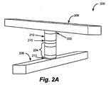
メモリセルの第1の例示的な実施形態
図2Aは、本発明に従って提供されるメモリセル200の第1の実施形態の略斜視図である。図2Aを参照して、メモリセル200は、第1の導体206と第2の導体208との間にダイオード204と直列に接続される可逆的抵抗スイッチング素子202を含む。ある実施形態では、可逆的抵抗スイッチング素子202とダイオード204との間に、バリア層210および/または導電層212が形成されてもよい。例えば、バリア層210は、窒化チタン、窒化タンタル、窒化タングステンなどを含んでもよく、導電層212は、タングステンまたは別の適切な金属層を含んでもよい。以下にさらに説明するように、バリア層210および/または導電層212は、ダイオード204を形成する過程でハードマスクとして働いてもよい。このようなハードマスクは、例えば、その全体が本願明細書において参照により援用されている、2006年5月13日に出願された「CONDUCTIVE HARD MASK TO PROTECT PATTERNED FEATURES DURING TRENCH ETCH」という米国特許出願第11/444,936号(特許文献7)に記載されている。ダイオード204と第1の導体206との間には、窒化チタン、窒化タンタル、窒化タングステンなどの追加のバリア層213も形成されてよい。
First Exemplary Embodiment of Memory Cell FIG. 2A is a schematic perspective view of a first embodiment of a
以下にさらに説明するように、可逆的抵抗スイッチング素子202は、メモリセル200の製造を簡略化するように、選択的に形成される。少なくとも1つの実施形態では、可逆的抵抗スイッチング素子202は、ニッケルを選択的に付着させ、次いでニッケル層を酸化することによって形成される酸化ニッケル層の少なくとも一部を含む。例えば、Ni、Nix Py またはニッケルの別の形態が、非電解析出、電気メッキまたは類似の選択プロセスを使用して選択的に付着され、次いで(例えば、急速熱酸化または他の酸化プロセスを使用して)酸化されて酸化ニッケルを形成してもよい。他の実施形態では、酸化ニッケル自体が選択的に付着されてもよい。例えば、NiO、NiOx またはNiOx Py 含有層が、選択付着プロセスを使用してダイオード204の上に選択的に付着され、次いで(必要に応じて)アニールおよび/または酸化されてもよい。これらの実施形態および他の実施形態は、図3を参照しながら以下にさらに説明する。図2Aでは、可逆的抵抗スイッチング素子202は、ダイオード204の上に位置するように示されるが、当然ながら、代替の実施形態では、可逆的抵抗スイッチング素子202は、(例えば、図6を参照して以下に説明するように)ダイオード204の下に位置してもよい。ある実施形態では、可逆的抵抗スイッチング素子202の1つ以上のフィラメントなどの部分のみがスイッチングしても、および/またはスイッチング可能であってもよい。
As described further below, the reversible
ダイオード204は、ダイオードのp領域の上にn領域を有して上を向くか、ダイオードのn領域の上にp領域を有して下を向くかによらず、垂直多結晶p−nまたはp−i−nダイオードなどの何らかの適切なダイオードを含んでもよい。ダイオード204の例示的な実施形態は、図3を参照しながら以下に説明する。
Regardless of whether the
第1および/または第2の導体206、208は、タングステン、何らかの適切な金属、高濃度にドープされた半導体材料、導電性シリサイド、導電性シリサイド−ゲルマニド、導電性ゲルマニドなどの何らかの適切な導電性材料を含んでもよい。図2Aの実施形態では、第1および/または第2の導体206、208は、レール状で、(例えば、実質的に互いに直交して)異なる方向に延びる。他の導体形状および/または構造が使用されてもよい。ある実施形態では、第1および/または第2の導体206、208とともに、バリア層、接着層、反射防止コーティングおよび/またはその類似物(図示せず)が使用され、デバイス性能を改善し、および/またはデバイスの製造に役立てることもできる。
The first and / or
前述したように、他の材料を使用して、可逆的抵抗スイッチング素子202を形成してもよい。例えば、Nb、Ta、V、Al、Ti、Co、コバルト−ニッケル合金などの材料が、同様に、(図2Aに示されるように、バリア層210の上および/または導電層212の上などの)ダイオード204の上に選択的に付着され、必要に応じて酸化および/またはアニールされて、可逆的抵抗スイッチング素子202を形成してもよい。
As described above, other materials may be used to form the reversible
図2Bは、複数の図2Aのメモリセル200から形成される第1のメモリレベル214の一部の略斜視図である。簡単にするため、可逆的抵抗スイッチング素子202、ダイオード204、バリア層210および213、および導電層212は、個別に示されない。メモリアレイ214は、(図に示されるように)複数のメモリセルが接続される複数のビット線(第2の導体208)およびワード線(第1の導体206)を含む「クロスポイント」アレイである。他のメモリアレイ構造が、マルチレベルのメモリとして使用されてもよい。例えば、図2Cは、第2のメモリレベル220の下に配置される第1のメモリレベル218を含むモノリシックな3次元アレイ216の一部の略斜視図である。図2Cの実施形態では、各メモリレベル218、220は、クロスポイントアレイ内に複数のメモリセル200を含む。当然ながら、第1のメモリレベル218と第2のメモリレベル220との間に、追加の層(例えば、中間誘電体)が存在してもよいが、簡単にするために図2Cでは示されない。他のメモリアレイ構造が、メモリの追加レベルとして使用されてもよい。図2Cの実施形態では、すべてのダイオードは、p型領域を有するp−i−nダイオードがダイオードの下部に使用されるか上部に使用されるかによって、上向きまたは下向きなどの同じ方向に「向く」ことで、ダイオードの製造を簡略化することもできる。
FIG. 2B is a schematic perspective view of a portion of a
ある実施形態では、メモリレベルは、例えば、あらゆる点でその全体が本願明細書において参照により援用されている「High-density three-dimensional memory cell」という米国特許第6,952,030号(特許文献8)で説明されるように形成されてもよい。例えば、図2Dに示されるように、第1のメモリレベルの上部導体は、第1のメモリレベルの上に位置する第2のメモリレベルの下部導体として用いられてもよい。この実施形態では、あらゆる点でその全体が本願明細書において参照により援用されている、2007年3月27日に出願された「LARGE ARRAY OF UPWARD POINTING P-I-N DIODES HAVING LARGE AND UNIFORM CURRENT」という米国特許出願第11/692,151号(特許文献9)で説明されるように、隣接するメモリレベル上のダイオードは、反対方向に向くのが好ましい。例えば、第1のメモリレベル218のダイオードは、(例えば、ダイオードの下部にp領域を有して)矢印A1で示されるように上向きダイオードであってもよく、第2のメモリレベル220のダイオードは、(例えば、ダイオードの下部にn領域を有して)矢印A2で示されるように下向きダイオードであってもよく、あるいはその逆であってもよい。
In one embodiment, the memory level is, for example, US Pat. No. 6,952,030, “High-density three-dimensional memory cell”, which is incorporated herein by reference in its entirety. It may be formed as described in 8). For example, as shown in FIG. 2D, the first memory level upper conductor may be used as a second memory level lower conductor located above the first memory level. In this embodiment, a US patent application entitled “LARGE ARRAY OF UPWARD POINTING PIN DIODES HAVING LARGE AND UNIFORM CURRENT” filed Mar. 27, 2007, which is incorporated herein by reference in its entirety. As described in US Patent No. 11 / 692,151, the diodes on adjacent memory levels are preferably oriented in the opposite direction. For example, the
モノリシックな3次元メモリアレイは、複数のメモリレベルが、中間基板を用いないでウェハなどの単一の基板上に形成されるアレイである。1つのメモリレベルを形成する層は、既存のレベル(単数または複数)の層の上に直接付着または成長される。これに対して、積層メモリは、Leedy による「Three dimensional structure memory」という米国特許第5,915,167号(特許文献10)の場合のように、別々の基板上にメモリレベルを形成し、そのメモリレベルを互いに重ねて接着することによって構築されている。基板は、ボンディングの前に薄くされても、あるいはメモリレベルから取り除かれてもよいが、メモリレベルが個別の基板上に最初に形成されるので、このようなメモリは、本当のモノリシックな3次元メモリアレイではない。 A monolithic three-dimensional memory array is an array in which multiple memory levels are formed on a single substrate, such as a wafer, without using an intermediate substrate. The layers that form a memory level are deposited or grown directly on the existing level or layers. On the other hand, the stacked memory forms memory levels on different substrates, as in US Pat. No. 5,915,167 (“Patent Document 10”) called “Three dimensional structure memory” by Leedy. It is built by stacking and bonding memory levels on top of each other. The substrate may be thinned prior to bonding or removed from the memory level, but such a memory is a true monolithic 3D because the memory level is first formed on a separate substrate. It is not a memory array.
図3は、図2Aのメモリセル200の例示的な実施形態の断面図である。図3を参照して、メモリセル200は、可逆的抵抗スイッチング素子202と、ダイオード204と、第1および第2の導体206、208とを含む。
前述したように、ダイオード204は、垂直p−nまたはp−i−nダイオードであってもよく、このダイオードは上向きでも下向きでもよい。隣接するメモリレベルが導体を共有する図2Dの実施形態では、隣接するメモリレベルは、第1のメモリレベルには下向きのp−i−nダイオード、隣接する第2のメモリレベルには上向きのp−i−nダイオード(あるいは、その逆)のように反対方向を向くダイオードを有するのが好ましい。
FIG. 3 is a cross-sectional view of an exemplary embodiment of the
As previously described, the
ある実施形態では、ダイオード204は、ポリシリコン、多結晶シリコン−ゲルマニウム合金、ポリゲルマニウム、または他の何らかの適切な材料などの多結晶半導体材料から形成されてもよい。例えば、ダイオード204は、高濃度にドープされたn+ポリシリコン領域302と、n+ポリシリコン領域302の上の低濃度にドープされたまたは真性(自然にドープされた)ポリシリコン領域304と、真性領域304の上の高濃度にドープされたp+ポリシリコン領域306とを含んでもよい。ある実施形態では、例えば、あらゆる点でその全体が本願明細書において参照により援用されている、2005年12月9日に出願された「DEPOSITED SEMICONDUCTOR STRUCTURE TO MINIMIZE N-TYPE DOPANT DIFFUSION AND METHOD OF MAKING」という米国特許出願第11/298,331号(特許文献11)で説明されるように、シリコン−ゲルマニウム合金層を使用する場合、約10at%(アトミックパーセント)以上のゲルマニウムを有する薄い(例えば、数百オングストローム以下の)ゲルマニウムおよび/またはシリコン−ゲルマニウム合金層(図示せず)をn+ポリシリコン領域302上に形成し、n+ポリシリコン領域302から真性領域304内へのドーパントの移動を防止および/または低減することもできる。当然ながら、n+およびp+領域の位置は逆であってもよい。(例えば、ポリシリコン領域内への金属原子の移動を防止および/または低減するために)第1の導体206とn+領域302との間に、窒化チタン、窒化タンタル、窒化タングステンなどのバリア層308が形成されてもよい。
In some embodiments,
ダイオード204が、付着シリコン(例えば、非晶質または多結晶)から形成される場合、ダイオード204上にシリサイド層310を形成して、付着シリコンを製造時の低抵抗率状態に置いてもよい。この低抵抗率状態によって、付着シリコンを低抵抗率状態に切り換えるのに高い電圧は必要ないため、メモリセル200のプログラミングを容易にすることができる。例えば、p+ポリシリコン領域306上に、チタンまたはコバルトなどのシリサイド形成金属層312が付着されてもよい。ダイオード204を形成する付着シリコンを結晶化するのに使用される(以下に説明する)次のアニールステップの過程で、シリサイド形成金属層312とダイオード204の付着シリコンとが相互に作用してシリサイド層310を形成し、これがシリサイド形成金属層312のすべてまたは一部を占める。
If the
その全体が本願明細書において参照により援用されている「Memory Cell Comprising a Semiconductor Junction Diode Crystallized Adjacent to a Silicide 」という米国特許第7,176,064号(特許文献12)に記載されるように、チタンおよび/またはコバルトなどのシリサイド形成材料は、アニール中に付着シリコンと反応してシリサイド層を形成する。チタンシリサイドおよびコバルトシリサイドの格子間隔は、シリコンの格子間隔に近く、このようなシリサイド層は、付着シリコンが結晶化する場合、隣接する付着シリコンの「結晶化テンプレート」または「シード」として働くこともできる(例えば、シリサイド層310は、アニール中にシリコンダイオード204の結晶構造を強化する)ようである。これによって、低抵抗率シリコンが提供される。シリコン−ゲルマニウム合金および/またはゲルマニウムダイオードについても、同様な結果を得ることもできる。
As described in US Pat. No. 7,176,064 (Patent Document 12) entitled “Memory Cell Comprising a Semiconductor Junction Diode Crystallized Adjacent to a Silicide”, which is incorporated by reference herein in its entirety. And / or a silicide-forming material such as cobalt reacts with the deposited silicon during annealing to form a silicide layer. The lattice spacing of titanium silicide and cobalt silicide is close to that of silicon, and such a silicide layer can also act as a “crystallization template” or “seed” for adjacent deposited silicon when the deposited silicon crystallizes. It seems possible (eg,
図3の実施形態では、可逆的抵抗スイッチング素子202は、選択付着プロセスによって形成される。ある実施形態では、可逆的抵抗スイッチング素子202は、導電性シリサイド形成金属層312の上に(またはシリサイド形成金属層312の上に形成される導電性バリア層の上に)形成されてもよい。(図4A〜図4Dを参照しながら以下に説明するように、このような層は、ダイオード204の形成中にパターニングされてもよい)。しかし、他の実施形態では、可逆的抵抗スイッチング素子202を形成する前に、シリサイド形成金属層312の上に金属ハードマスクが形成されてもよい。例えば、シリサイド形成金属層312の上に、バリア層314および/または導電層316が形成されてもよい。バリア層314は、窒化チタン、窒化タンタル、窒化タングステンなどを含んでもよく、導電層316は、タングステンまたは別の適切な金属層を含んでもよい。以下にさらに説明するように、バリア層314および/または導電層316は、ダイオード204の形成中にハードマスクとして働いてもよく、(前に援用されている特許文献7に記載されるように)上部導体208を形成する過程で発生し得るあらゆるオーバーエッチングを軽減することもできる。例えば、バリア層314および導電層316は、パターニングおよびエッチングされ、その後ダイオード204のエッチング中にマスクとして働いてもよい。導電層316、バリア層314、シリサイド形成金属層312、ダイオード204(p+ポリシリコン層306、真性層304、n+ポリシリコン層302)およびバリア層308をエッチングして、ピラー構造318が作られる。メモリセル200を含むメモリレベル上に製造される他のメモリセル(図示せず)の他の類似のピラー構造からピラー構造318を分離するように、ピラー構造318の上およびその周囲には、誘電材料320が付着される。次いで、CMPまたは誘電体エッチバックステップが実施され、誘電材料320を平坦化し、導電層316の上端部から誘電材料を取り除く。
In the embodiment of FIG. 3, the reversible
誘電材料320の平坦化の後、パターニングされエッチングされた導電層316の上に、選択付着プロセスによって可逆的抵抗スイッチング素子202が形成されてもよい。例えば、パターニングされエッチングされた導電層316の上に、(1)NiO、NiOx 、NiOx Py などの酸化ニッケルを選択的に付着させ、必要に応じて、酸化ニッケルをアニールおよび/または酸化し、および/または(2)ニッケルを選択的に付着させ、次いでニッケルを酸化することによって、酸化ニッケル層が選択的に形成されてもよい。どちらの場合も、酸化ニッケルは、パターニングされエッチングされた導電層316の上面にのみ付着するため、ニッケルおよび/または酸化ニッケル層をエッチングする必要がなくなり、メモリセルの製造を大幅に簡略化することもできる。さらに、所望のあらゆる厚さの酸化ニッケルを形成することもできる。ある実施形態では、可逆的抵抗スイッチング素子202に、約1,000オングストローム以下、さらに好ましくは、約500オングストローム以下の厚さの酸化ニッケル層が使用される(ただし、他の層厚範囲が使用されてもよい)。
After planarization of the
一実施形態では、導電層316の形成、パターニングおよびエッチングの後、無電解付着プロセスが使用され、導電層316の上にニッケルまたは酸化ニッケルを選択的に付着させる。例えば、水溶液を使用し導電層316を水溶液に浸すことによって、導電層316の上にニッケルまたは酸化ニッケルを選択的に形成してもよい。水溶液は、例えば、溶液のpHを調整するための1つ以上の溶解塩/前駆物質、錯化剤および/または緩衝液を含んでもよい。ある実施形態では、水溶液は、硫酸ニッケル、亜硫酸ニッケル、リン酸ニッケル、亜リン酸ニッケル、水酸化ニッケル、リン酸アンモニア、またはその混合物などのニッケル塩および/または水酸化ニッケル塩を含んでもよい。さらに例示的な組成は、NiSO4 、NaH2 PO2 、クエン酸ナトリウム、(NH4 )2 SO4 、またはその類似物を含んでもよい。当然ながら、水溶液および/または他のプロセス条件を形成するのに使用される正確な組成に応じて、導電層316の上にニッケルか酸化ニッケルのどちらか(またはその両方)が付着されてもよい。
In one embodiment, after formation, patterning and etching of
例示的なプロセス条件は、ニッケル含有水溶液を約20から85℃の間の温度に維持しながら、導電層316をその水溶液中に約1秒から約5分間浸すステップを含む。あらゆる点でその全体が本願明細書において参照により援用されている、N. Takano et al., "Mechanism of the Chemical Deposition of Nickel on Silicon Wafers in Aqueous Solution", Journal of Electrochemical Society, 146(4) pp. 1407-1411 (1999) (非特許文献1)には、ニッケルまたは酸化ニッケル層を選択的に形成するのに使用される追加の例示的な水溶液および/またはプロセス条件が記載されている。前述したように、付着ニッケルまたは酸化ニッケルは、Ni、Nix Py 、NiO、NiOx 、NiOx Py 、または他の類似の材料を含んでもよい。
Exemplary process conditions include immersing the
ニッケルまたは酸化ニッケルの形成に続いて、熱酸化プロセスを使用して、選択付着ニッケルから酸化ニッケルを形成するか、あるいは選択付着酸化ニッケルの形態および/または電気的特性を改善するかのどちらかを行ってもよい。例示的な酸化条件は、約400から800℃の温度による約20秒から10分間のO2 などの酸素雰囲気中での急速熱酸化を含む。他の酸化またはアニールプロセス、酸素種、時間および/または温度が使用されてもよい。 Following the formation of nickel or nickel oxide, either a thermal oxidation process is used to form nickel oxide from the selectively deposited nickel or to improve the morphology and / or electrical properties of the selectively deposited nickel oxide. You may go. Exemplary oxidation conditions include rapid thermal oxidation in an oxygen atmosphere such as O 2 for about 20 seconds to 10 minutes at a temperature of about 400 to 800 ° C. Other oxidation or annealing processes, oxygen species, time and / or temperature may be used.
パターニングおよびエッチングされた導電層316の上にニッケル含有層を形成するのに使用されてもよい別の適切な選択付着プロセスは、従来のニッケル電気メッキを含む。いかなる適切な電気メッキプロセスを使用して、導電層316の上にニッケルを選択的に付着させてもよい。その後、前述したように、電気メッキされたニッケルを酸化して酸化ニッケルを形成してもよい。
Another suitable selective deposition process that may be used to form a nickel-containing layer over the patterned and etched
前述したように、他の材料を使用して可逆的抵抗スイッチング素子202を形成してもよい。例えば、Nb、Ta、V、Al、Ti、Co、コバルト−ニッケル合金などの材料が、同様に、(図2Aに示されるように、バリア層210の上および/または導電層212の上などの)ダイオード204の上に選択的に付着され、必要に応じて酸化および/またはアニールされてもよい。
As described above, the reversible
可逆的抵抗スイッチング素子202の形成に続いて、上部導体208が形成される。ある実施形態では、導電層324を付着する前に1つ以上のバリア層および/または接着層322が、可逆的抵抗スイッチング素子202の上に形成されてもよい。導電層324とバリア層322とが、一緒にパターニングおよび/またはエッチングされて上部導体208を形成してもよい。ある実施形態では、図4A〜図4Dを参照して以下に説明するように、ダマシンプロセスを使用して上部導体208が形成されてもよい。
Following formation of the reversible
上部導体208の形成に続いて、メモリセル200をアニールして、ダイオード204の付着半導体材料を結晶化(および/または、シリサイド層310を形成)してもよい。少なくとも1つの実施形態では、アニールは、約10秒から約2分間、約600から800℃の温度、さらに好ましくは、約650から750℃の間の温度の窒素中で実施されてもよい。他のアニール時間、温度および/または雰囲気が使用されてもよい。前述したように、シリサイド層310は、アニール中に、ダイオード204を形成する下の付着半導体材料の「結晶化テンプレート」または「シード」として働くこともできる。これによって、低抵抗率ダイオード材料が提供される。
Following formation of the
本発明に従ってメモリセルを製造する例示的なプロセスを図4A〜図4Dを参照しながら以下に説明する。 An exemplary process for manufacturing a memory cell according to the present invention is described below with reference to FIGS. 4A-4D.
メモリセルの例示的な製造プロセス
図4A〜図4Dは、本発明に従って第1のメモリレベルを製造する過程の基板400の一部の断面図を示す。以下に説明するように、第1のメモリレベルは、選択付着プロセスを使用して形成される可逆的抵抗スイッチング素子をそれぞれ含む複数のメモリセルを含む。(図2C〜図2Dを参照して前に説明したように)第1のメモリレベルの上には追加のメモリレベルが製造されてもよい。
Exemplary Manufacturing Process of Memory Cell FIGS. 4A-4D illustrate a cross-sectional view of a portion of a
図4Aを参照して、基板400は、幾つかの処理ステップが既に施されたものとして示される。基板400は、追加回路の有無にかかわらず、シリコン、ゲルマニウム、シリコン−ゲルマニウム、非ドープ、ドープ、バルク、シリコンオンインシュレータ(SOI)または他の基板などのどんな適切な基板でもよい。例えば、基板400は、1つ以上のnウェルまたはpウェル領域(図示せず)を含んでもよい。
With reference to FIG. 4A, the
基板400の上には、絶縁層402が形成される。ある実施形態では、絶縁層402は、二酸化シリコン、窒化シリコン、酸窒化シリコン、または他の適切な絶縁層であってもよい。
An insulating
絶縁層402の形成に続いて、(例えば、物理気相付着法または別の方法によって)絶縁層402の上に接着層404が形成される。例えば、接着層404は、約20から約500オングストローム、好ましくは、約100オングストロームの窒化チタン、または窒化タンタル、窒化タングステン、1つ以上の接着層の組み合わせ、またはその類似物などの別の適切な接着層であってもよい。他の接着層の材料および/または厚さが使用されてもよい。ある実施形態では、接着層404は任意であってもよい。
Following formation of the insulating
接着層404の形成に続いて、接着層404の上に導電層406が付着される。導電層406は、タングステンまたは別の適切な金属、高濃度にドープされた半導体材料、導電性シリサイド、導電性シリサイド−ゲルマニド、導電性ゲルマニド、または何らかの適切な方法(例えば、化学気相付着(CVD)、物理気相付着(PVD)など)によって付着される類似物などの何らかの適切な導電性材料を含んでもよい。少なくとも1つの実施形態では、導電層406は、約200から約2,500オングストロームのタングステンを含んでもよい。他の導電層の材料および/または厚さが使用されてもよい。
Following formation of the
導電層406の形成に続いて、接着層404および導電層406がパターニングされエッチングされる。例えば、接着層404および導電層406は、ソフトまたはハードマスク、およびウェットまたはドライエッチングプロセスを用いる従来のリソグラフィ技術を使用してパターニングされエッチングされてもよい。少なくとも1つの実施形態では、接着層404および導電層406は、実質的に平行で実質的に共平面の導体408(図4Aに示される)を形成するように、パターニングされエッチングされる。例示的な導体408の幅および/または導体408同士の間隔は、約200から約2500オングストロームの範囲であるが、他の導体の幅および/または間隔が使用されてもよい。
Following the formation of the
導体408が形成された後、導体408間の隙間を充填するように、基板400の上に誘電層410が形成される。例えば、基板400上にほぼ3,000から7,000オングストロームの二酸化シリコンが付着され、化学的機械的研磨またはエッチバックプロセスを使用して平坦化されて平面412を形成してもよい。(図に示されるように)平面412は、誘電材料によって分離される導体408の露出された上面を含む。窒化シリコン、酸窒化シリコン、低誘電率(low K)誘電体などの他の誘電材料、および/または他の誘電層厚が使用されてもよい。例示的なlow K誘電体は、炭素ドープ酸化物、シリコン炭素層、またはその類似物を含む。
After the
本発明の他の実施形態では、ダマシンプロセスを使用して導体408が形成されてもよいが、その場合、誘電層410が形成されパターニングされて導体408のための開口部または隙間が作られる。次いで、開口部または隙間は、接着層404および導電層406(および/または導電性シード、導電性フィルおよび/または必要に応じてバリア層)で充填されてもよい。次いで、接着層404および導電層406は、平坦化されて平面412を形成してもよい。この実施形態では、接着層404は、各開口部または隙間の底部および側壁を内張りする。
In other embodiments of the invention,
平坦化に続いて、各メモリセルのダイオード構造が形成される。図4Bを参照して、基板400の平坦化された上面412の上にバリア層414が形成される。バリア層414は、約20から約500オングストローム、好ましくは、約100オングストロームの窒化チタン、あるいは、窒化タンタル、窒化タングステン、1つ以上のバリア層の組み合わせ、チタン/窒化チタン、タンタル/窒化タンタルまたはタングステン/窒化タングステンの積層などの他の層と組み合わせたバリア層、またはその類似物などの別の適切なバリア層であってもよい。他のバリア層の材料および/または厚さが使用されてもよい。
Following planarization, a diode structure for each memory cell is formed. Referring to FIG. 4B, a
バリア層414の付着の後で、各メモリセルのダイオード(例えば、図2A〜図3のダイオード204)を形成するのに使用される半導体材料の付着が開始される。各ダイオードは、前に説明したように、垂直p−nまたはp−i−nダイオードであってもよい。ある実施形態では、各ダイオードは、ポリシリコン、多結晶シリコン−ゲルマニウム合金、ポリゲルマニウムまたは他の何らかの適切な材料などの多結晶半導体材料から形成される。便宜上、本願明細書では、ポリシリコンによる下向きのダイオードの形成について説明する。当然ながら、他の材料および/またはダイオード構造が使用されてもよい。
After deposition of the
図4Bを参照して、バリア層414の形成に続いて、バリア層414上に高濃度にドープされたn+シリコン層416が付着される。ある実施形態では、n+シリコン層416は、付着時に非晶質状態にある。他の実施形態では、n+シリコン層416は、付着時に多結晶状態にある。CVDまたは別の適切なプロセスを使用して、n+シリコン層416を付着してもよい。少なくとも1つの実施形態では、n+シリコン層416は、例えば、約1021cm-3のドーピング濃度を有する約100から約1000オングストローム、好ましくは、約100オングストロームのリンまたはヒ素ドープシリコンから形成されてもよい。他の層厚、ドーピング型および/またはドーピング濃度が使用されてもよい。n+シリコン層416は、例えば、付着中にドナーガスを流すことによって、その場で(in situ) ドープされてもよい。他のドーピング方法が使用されてもよい(例えば、注入法)。
Referring to FIG. 4B, following the formation of
n+シリコン層416の付着の後で、n+シリコン層416の上に低濃度にドープされた真性シリコン層および/または自然にドープされたシリコン層418が形成される。ある実施形態では、真性シリコン層418は、付着時に非晶質状態にある。他の実施形態では、真性シリコン層418は、付着時に多結晶状態にある。CVDまたは別の適切な付着方法を使用して、真性シリコン層418を付着してもよい。少なくとも1つの実施形態では、真性シリコン層418は、厚さが約500から約4,800オングストローム、好ましくは、約2,500オングストロームであってもよい。他の真性層厚が使用されてもよい。
After deposition of the n +
(前に援用されている特許文献11に記載されるように)真性シリコン層418を付着する前に、n+シリコン層416の上に薄い(例えば、数百オングストローム以下の)ゲルマニウムおよび/またはシリコン−ゲルマニウム合金層(図示せず)を形成して、n+シリコン層416から真性シリコン層418内へのドーパントの移動を防止および/または低減してもよい。
Before depositing the intrinsic silicon layer 418 (as described in previously incorporated US Pat. No. 6,057,049), thin (eg, less than a few hundred angstroms) germanium and / or silicon − on the n + silicon layer 416 A germanium alloy layer (not shown) may be formed to prevent and / or reduce dopant migration from the n +
高濃度にドープされたp型シリコンが付着されイオン注入によってドープされるか、あるいは付着中にその場でドープされてp+シリコン層420を形成する。例えば、ブランケットp+注入を使用して、真性シリコン層418内に所定の深さでボロンを注入してもよい。例示的な注入可能分子イオンは、BF2 、BF3 、Bなどを含む。ある実施形態では、約1〜5×10¹⁵イオン/cm2 の注入ドーズ量が使用されてもよい。他の注入種および/またはドーズ量が使用されてもよい。さらに、ある実施形態では、拡散プロセスが使用されてもよい。少なくとも1つの実施形態では、その結果得られるP+シリコン領域420は、約100から700オングストロームの厚さを有するが、他のP+シリコン層サイズが使用されてもよい。
Highly doped p-type silicon is deposited and doped by ion implantation or doped in situ during deposition to form p +
p+シリコン層420の形成に続いて、p+シリコン層420の上にシリサイド形成金属層422が付着される。例示的なシリサイド形成金属は、スパッタあるいは付着チタンまたはコバルトを含む。ある実施形態では、シリサイド形成金属層422は、約10から約200オングストローム、好ましくは、約20から約50オングストローム、さらに好ましくは、約20オングストロームの厚さを有する。他のシリサイド形成金属層の材料および/または厚さが使用されてもよい。
Following formation of the p +
シリサイド形成金属層422の上に、バリア層424が付着される。バリア層424は、約20から約500オングストローム、好ましくは、約100オングストロームの窒化チタン、あるいは、窒化タンタル、窒化タングステン、1つ以上のバリア層の組み合わせ、チタン/窒化チタン、タンタル/窒化タンタルまたはタングステン/窒化タングステンの積層などの他の層と組み合わせたバリア層、またはその類似物などの別の適切なバリア層であってもよい。他のバリア層の材料および/または厚さが使用されてもよい。
A
バリア層424の形成に続いて、バリア層424の上に導電層426が形成される。導電層426は、約50から約1000オングストローム、好ましくは、約500オングストロームのタングステンなどの導電性材料または別の適切な金属であってもよい。
Following the formation of the
次いで、バリア層414、シリコン領域416、418および420、シリサイド形成金属層422、バリア層424ならびに導電層426は、パターニングされエッチングされてピラー428になる。例えば、最初に、導電層426およびバリア層424がエッチングされる。エッチングは続いて、シリサイド形成金属層422、シリコン領域420、418および416ならびにバリア層414をエッチングする。導電層426およびバリア層414は、シリコンのエッチング中にハードマスクとして働く。ハードマスクは、その下の層のエッチングをパターニングする働きをするエッチング層であり、導電層426上に存在するすべてのフォトレジストが使用された場合、それの代わりにハードマスクはパターンを提供することができる。このように、ピラー428は、単一のフォトリソグラフィステップで形成される。従来のリソグラフィ技術およびウェットまたはドライエッチング処理を使用してピラー428を形成してもよい。各ピラー428は、p−i−n下向きダイオード430を含む。上向きp−i−nダイオードが同様に形成されてもよい。
The
ピラー428が形成された後、ピラー428間の隙間を充填するためにピラー428の上に誘電層432が付着される。例えば、約200から7,000オングストロームの二酸化シリコンが付着され、化学的機械的研磨またはエッチバックプロセスを使用して平坦化され、平面434を形成してもよい。平面434は、(図に示されるように)誘電材料432によって分離されるピラー428の露出された上面を含む。窒化シリコン、酸窒化シリコン、low K誘電体などの他の誘電材料、および/または他の誘電層厚が使用されてもよい。例示的なlow K誘電体は、炭素ドープ酸化物、シリコン炭素層、またはその類似物を含む。
After the
平面434の形成に続いて、各ピラー428の上に可逆的抵抗スイッチング素子436(図4C)が選択的に形成される。例えば、(1)酸化ニッケルを選択的に付着させる、および/または(2)ニッケルを選択的に付着させてからそのニッケルを酸化することによって、酸化ニッケル層が各導電性ピラー428の上に選択的に形成されてもよい。どちらの場合も、ニッケルおよび/または酸化ニッケル層をエッチングする必要がなくなり、メモリセルの製造を大幅に簡略化することもできる。前に説明したように、無電解付着、電気メッキまたはその類似の方法などのニッケルまたは酸化ニッケルを選択的に付着するためのいかなる適切な方法が使用されてもよい。少なくとも1つの実施形態では、各導電性ピラー428の上に形成される可逆的抵抗スイッチング素子436は、約1,000オングストローム以下の厚さ、より好ましくは、約500オングストローム以下の厚さを有する酸化ニッケル層を含む。他の酸化ニッケル層厚が使用されてもよい。酸化ニッケル層は、例えば、NiO、NiOx およびNiOx Py または他の類似の材料を含んでもよい。Nb、Ta、V、Al、Ti、Co、コバルト−ニッケル合金などの他の材料が、同様に、選択的に付着され、酸化および/またはアニールされて、各ピラー428の上に選択付着による可逆的抵抗スイッチング素子を形成してもよい。
Following the formation of the
図4Dを参照して、可逆的抵抗スイッチング素子436の形成に続いて、第2の一連の導体438が、下部の一連の導体408の形成と同様な方法でピラー428の上に形成されてもよい。例えば、図4Dに示されるように、ある実施形態では、上部の第2の一連の導体438を形成するのに使用される導体層442を付着させる前に、可逆的抵抗スイッチング素子436の上に1つ以上のバリア層および/または接着層440が付着されてもよい。
Referring to FIG. 4D, following formation of the reversible
導電層442は、タングステン、別の適切な金属、高濃度にドープされた半導体材料、導電性シリサイド、導電性シリサイド−ゲルマニド、導電性ゲルマニド、または何らかの適切な方法(例えば、CVD、PVDなど)によって付着される類似物などの何らかの適切な導電性材料から形成されてもよい。他の導電層材料が使用されてもよい。バリア層および/または接着層440は、窒化チタン、あるいは窒化タンタル、窒化タングステン、1つ以上の層の組み合わせ、または他の何らかの適切な材料(単数または複数)などの別の適切な層を含んでもよい。付着された導電性層442およびバリアおよび/または接着層440は、パターニングおよびエッチングされて第2の一連の導体438を形成する。少なくとも1つの実施形態では、上部導体438は、下部導体408と異なる方向に延びる実質的に平行で実質的に共平面の導体である。
本発明の他の実施形態では、ダマシンプロセスを使用して上部導体438が形成されてもよいが、その場合、誘電層が形成されパターニングされて導体438のための開口部または隙間が作られる。特許文献7に記載されるように、導電層426およびバリア層424は、上部導体438のための開口部または隙間を形成する過程でこの誘電層をオーバーエッチングする作用を軽減し、ダイオード430が誤って短絡するのを防ぐこともできる。
In other embodiments of the invention, the
開口部または隙間は、接着層440および導電層442(および/または導電性シード、導電性フィルおよび/または必要に応じてバリア層)で充填されてもよい。次いで、接着層440および導電層442は、平坦化されて平面を形成してもよい。
The openings or gaps may be filled with an
上部導体438の形成に続いて、本構造をアニールして、ダイオード430の付着半導体材料を結晶化(および/またはシリサイド形成金属層422とp+領域420との反応によってシリサイド領域を形成)してもよい。少なくとも1つの実施形態では、アニールは、約600から800℃、さらに好ましくは、約650から750℃の間の温度の窒素中で、約10秒から約2分間実施されてもよい。他のアニール時間、温度および/または雰囲気が使用されてもよい。シリサイド形成金属層領域422とp+領域420とがそれぞれ反応して形成されるシリサイド領域は、アニール中にダイオード430を形成する下の付着半導体材料の「結晶化テンプレート」または「シード」として働くこともできる(例えば、何らかの非晶質半導体材料を多結晶半導体材料に変化させる、および/またはダイオード430の全体的な結晶特性を改善させる)。これによって、低抵抗率ダイオード材料が提供される。
Following formation of the
第1の代替の例示的なメモリセル
図5は、本発明に従って提供される例示的なメモリセル500の断面図である。メモリセル500は、基板505上に形成される可逆的抵抗スイッチング素子504に接続される薄膜金属酸化膜半導体電界効果トランジスタ(MOSFET)502などの薄膜トランジスタ(TFT)を含む。例えば、MOSFET502は、何らかの適切な基板上に形成されるnチャネルまたはpチャネル薄膜MOSFETであってもよい。図に示される実施形態では、二酸化シリコン、窒化シリコン、酸窒化物などの絶縁領域506が基板505上に形成され、絶縁領域506の上に、付着シリコン、ゲルマニウム、シリコン−ゲルマニウムなどの付着半導体領域507が形成される。付着半導体領域507内に薄膜MOSFET502が形成され、絶縁領域506によって基板505から分離される。
First Alternative Exemplary Memory Cell FIG. 5 is a cross-sectional view of an
MOSFET502は、ソース/ドレイン領域508、510およびチャネル領域512、ならびにゲート誘電層514、ゲート電極516およびスペーサ518a、518bを含む。少なくとも1つの実施形態では、ソース/ドレイン領域508、510はp型にドープされ、チャネル領域512はn型にドープされてもよく、他の実施形態では、ソース/ドレイン領域508、510はn型にドープされ、チャネル領域512はp型にドープされてもよい。薄膜MOSFET502には、他の何らかのMOSFET構造または何らかの適切な製造技術が使用されてもよい。ある実施形態では、MOSFET502は、STI、LOCOSまたは他の類似プロセスを使用して形成される絶縁領域(図示せず)によって電気的に分離されてもよい。あるいは、MOSFET502のゲート、ソースおよび/またはドレイン領域は、基板505上に形成される他のトランジスタ(図示せず)と共有されてもよい。
可逆的抵抗スイッチング素子504は、導電性プラグ526の上に形成される可逆的抵抗率スイッチング材料522を含む。少なくとも1つの実施形態では、可逆的抵抗スイッチング素子522は、図1〜図4Dの実施形態を参照しながら前に説明したように、選択付着プロセスを使用して形成される。例えば、(1)酸化ニッケルを選択的に付着させる、および/または(2)ニッケルを選択的に付着させてからそのニッケルを酸化することによって、酸化ニッケル層が導電性プラグ526の上に選択的に形成されてもよい。例示的な選択付着プロセスは、無電解付着、電気メッキ、またはその類似プロセスを含む。他の材料が本発明に従って選択的に付着され、酸化され、および/またはアニールされてメモリセル500で使用される可逆的抵抗率スイッチング材料を形成してもよい(例えば、Nb、Ta、V、Al、Ti、Co、コバルト−ニッケル合金など)。
The reversible
図5に示されるように、可逆的抵抗スイッチング素子504は、第1の導電性プラグ526によってMOSFET502のソース/ドレイン領域510に、第2の導電性プラグ530によって第1の金属レベル(M1)線528に接続される(これにより誘電層532を貫通して延びる)。同様に、第3の導電性プラグ534は、MOSFET502のソース/ドレイン領域508をM1線536に接続する。導電性プラグおよび/または線は、(バリア層の有無にかかわらず)タングステン、別の金属、高濃度にドープされた半導体材料、導電性シリサイド、導電性シリサイド−ゲルマニド、導電性ゲルマニドまたはその類似物などの何らかの適切な材料から形成されてもよい。MOSFET502がnチャネルデバイスの場合には、領域508はMOSFET502のドレイン、領域510はMOSFET502のソースとして機能し、MOSFET502がpチャネルデバイスの場合には、領域508はMOSFET502のソース、領域510はMOSFET502のドレインとして機能することに留意すべきである。誘電層532は、二酸化シリコン、窒化シリコン、酸窒化シリコン、low K誘電体などの何らかの適切な誘電体を含んでもよい。
As shown in FIG. 5, the reversible
メモリセル500で、薄膜MOSFET502は、図2A〜図4Dのメモリセルで使用されるダイオードのステアリング素子と同様な方法で、印加電圧および/または可逆的抵抗スイッチング素子504を通って流れる電流を選択的に制限するステアリング素子として動作する。
In
少なくとも1つの実施形態では、可逆的抵抗スイッチング素子504は、約1,000オングストローム以下、さらに好ましくは、約500オングストローム以下の厚さを有する酸化ニッケル層を含む。他の酸化ニッケル層厚が使用されてもよい。
In at least one embodiment, reversible
第2の代替のメモリセル
図6は、本発明に従って提供される例示的なメモリセル600の断面図である。メモリセル600は、可逆的抵抗スイッチング素子202がダイオード204の下に形成される点を除けば、図3のメモリセル200と類似している。具体的には、図6に示されるように、可逆的抵抗スイッチング素子202は、パターニングされエッチングされた下部導体206の上に導電性材料602を選択的に付着させることによって形成される。次いで、導電性材料602は、本発明に従って、必要に応じてアニールおよび/または酸化されてメモリセル600で使用される可逆的抵抗率スイッチング材料604を形成してもよい。例えば、導電性材料602は、電気メッキなどによって選択的に付着され、酸化されて可逆的抵抗率スイッチング材料層604を形成するNi、Nix Py 、NiO、NiOx 、NiOx Py 、Nb、Ta、V、Al、Ti、Co、コバルト−ニッケル合金などの層を含んでもよい。ダイオード204と垂直方向に重なりおよび/またはこれと位置合わせされる可逆的抵抗率スイッチング材料層604の一部は、メモリセル600のダイオード204と第1の導体206との間の可逆的抵抗スイッチング素子202として働いてもよい。ある実施形態では、可逆的抵抗スイッチング素子202の1つ以上のフィラメントなどの部分のみがスイッチングしても、および/またはスイッチング可能であってもよい。層604は、既にパターニングされエッチングされた下部導体206の上に選択的に付着されるため、可逆的抵抗率スイッチング材料層604はエッチングを必要としない。
Second Alternative Memory Cell FIG. 6 is a cross-sectional view of an exemplary memory cell 600 provided in accordance with the present invention. The memory cell 600 is similar to the
前述した説明は、本発明の例示的な実施形態のみを開示している。本発明の範囲に含まれる上で開示された装置および方法についての変更は、当業者であれば容易に思い当たるであろう。例えば、本発明は、主にニッケルおよび酸化ニッケルの選択付着に関して説明したが、当然ながら、例えば、Ta2 O5 、Nb2 O5 、Al2 O3 、V2 O5 、CoO、(Cox Niy )Oz 、およびTiO2 を形成するTa、Nb、Al、V、Co、コバルト−ニッケル合金、Tiなどの他の材料が選択的に付着され、可逆的抵抗スイッチング素子に使用されてもよい。
したがって、本発明は、その例示的な実施形態に関連して開示されたが、当然ながら、他の実施形態が、添付の特許請求の範囲によって定義される本発明の趣旨および範囲に含まれてもよい。
The foregoing description discloses only exemplary embodiments of the invention. Modifications to the apparatus and methods disclosed above that fall within the scope of the invention will be readily apparent to those skilled in the art. For example, the present invention has been described primarily in terms of selective deposition of nickel and nickel oxide, of course, for example, Ta 2 O 5, Nb 2 O 5, Al 2 O 3, V 2 O 5, CoO, (Co x Ni y ) O z and other materials such as Ta, Nb, Al, V, Co, cobalt-nickel alloy, Ti forming TiO 2 may be selectively deposited and used for reversible resistance switching elements. Good.
Thus, although the invention has been disclosed in connection with exemplary embodiments thereof, it is understood that other embodiments are encompassed within the spirit and scope of the invention as defined by the appended claims. Also good.
Claims (13)
基板上にステアリング素子を形成するステップと、
前記ステアリング素子に接続される可逆的抵抗スイッチング素子をエッチングすることなく、
a)導電層を形成し、
b)前記導電層をエッチングして、エッチングされた表面を形成し、かつ
c)そのエッチングされた表面上の前記可逆的抵抗スイッチング素子を無電解に付着するか、あるいは電気メッキすることにより、選択付着プロセスを使用して前記可逆的抵抗スイッチング素子を形成するステップと、
を含む方法。 A method of forming a memory cell, comprising:
Forming a steering element on the substrate;
Without etching the reversible resistance switching element connected to the steering element,
a) forming a conductive layer;
b) etching the conductive layer to form an etched surface; and
c) forming or attaching the reversible resistance-switching element on the etched surface in an electroless, or by electroplating, the reversible resistance-switching element using a selective deposition process,
Including methods.
前記ステアリング素子を形成するステップが、垂直多結晶ダイオードを形成するステップを含む方法。 The method of claim 1, wherein
Forming the steering element includes forming a vertical polycrystalline diode;
前記ステアリング素子を形成するステップが、p−nダイオードまたはp−i−nダイオードを形成するステップを含む方法。 The method of claim 1, wherein
Forming the steering element comprises forming a pn diode or a pin diode.
前記可逆的抵抗スイッチング素子を形成するステップが、NiO、NiOx およびNiOx Py のうちの少なくとも1つを形成するステップを含む方法。 The method of claim 1, wherein
Method comprising the step of forming at least one of the step of forming the reversible resistance-switching element, NiO, NiO x and NiO x P y.
前記可逆的抵抗スイッチング素子を形成するステップが、約1,000オングストローム以下の酸化層厚を有する可逆的抵抗スイッチング素子を形成するステップを含む方法。 The method of claim 4, wherein
Forming the reversible resistance switching element comprises forming a reversible resistance switching element having an oxide layer thickness of about 1,000 angstroms or less;
前記可逆的抵抗スイッチング素子を形成するステップが、ニッケル含有層を選択的に形成するステップを含む方法。 The method of claim 1, wherein
Forming the reversible resistance-switching element comprises selectively forming a nickel-containing layer.
前記ニッケル含有層を形成するステップが、NiO、NiOx またはNiOx Py 含有層を選択的に形成するステップを含む方法。 The method of claim 6 wherein:
Wherein forming the nickel-containing layer comprising the step of selectively forming NiO, NiO x or NiO x P y containing layer.
前記ニッケル含有層を形成するステップが、前記ニッケル含有層を無電解に付着するステップを含む方法。 The method of claim 7, wherein
Forming the nickel-containing layer comprises electrolessly depositing the nickel-containing layer.
前記ニッケル含有層を形成するステップが、電気メッキを使用して前記ニッケル含有層を形成するステップを含む方法。 The method of claim 7, wherein
The method of forming the nickel-containing layer includes forming the nickel-containing layer using electroplating.
前記可逆的抵抗スイッチング素子を形成するステップが、Ta2 O5 、Nb2 O5 、Al2 O3 、V2 O5 、CoO、(Cox Niy )Oz およびTiO2 のうちの少なくとも1つを形成するステップを含む方法。 The method of claim 1, wherein
The step of forming the reversible resistance-switching element, Ta 2 O 5, Nb 2 O 5, Al 2 O 3, V 2 O 5, CoO, (Co x Ni y) at least one of O z and TiO 2 A method comprising the steps of forming one.
基板上に形成される第1のメモリレベルを形成するステップであって、
ステアリング素子を形成し、かつ
前記ステアリング素子に接続される可逆的抵抗スイッチング素子をエッチングすることなく、
a)導電層を形成し、
b)前記導電層をエッチングして、エッチングされた表面を形成し、かつ
c)そのエッチングされた表面上の前記可逆的抵抗スイッチング素子を無電解に付着するか、あるいは電気メッキすることにより、選択付着プロセスを使用して前記可逆的抵抗スイッチング素子を形成することによって、複数のメモリセルの各メモリセルを形成することで、前記第1のメモリレベルを形成するステップと、
前記第1のメモリレベルの上にモノリシック的に形成される少なくとも第2のメモリレベルを形成するステップと、
を含む方法。 A method for forming a monolithic three-dimensional memory array comprising :
Forming a first memory level formed on a substrate , comprising:
Forming a steering element, and
Without etching the reversible resistance switching element connected to the steering element,
a) forming a conductive layer;
b) etching the conductive layer to form an etched surface; and
c) by forming the reversible resistance switching element using a selective deposition process by electrolessly depositing or electroplating the reversible resistance switching element on the etched surface; Forming the first memory level by forming each of the memory cells; and
Forming at least a second memory level that is monolithically formed on the first memory level;
Including methods .
各ステアリング素子が、垂直多結晶ダイオードを含む方法。 The method of claim 11 wherein:
Each steering element, the method comprising the vertical polycrystalline diode.
各可逆的抵抗スイッチング素子が、NiO、NiOx およびNiOx Py のうちの少なくとも1つを含む方法。 The method of claim 11 wherein:
Process comprising at least one of the reversible resistance-switching element, NiO, NiO x and NiO x P y.
Applications Claiming Priority (5)
| Application Number | Priority Date | Filing Date | Title |
|---|---|---|---|
| US11/772,090 | 2007-06-29 | ||
| US11/772,090 US7846785B2 (en) | 2007-06-29 | 2007-06-29 | Memory cell that employs a selectively deposited reversible resistance-switching element and methods of forming the same |
| US11/772,084 US8233308B2 (en) | 2007-06-29 | 2007-06-29 | Memory cell that employs a selectively deposited reversible resistance-switching element and methods of forming the same |
| US11/772,084 | 2007-06-29 | ||
| PCT/US2008/007986 WO2009005700A2 (en) | 2007-06-29 | 2008-06-27 | Memory cell that employs a selectively deposited reversible resistance-switching element and methods of forming the same |
Publications (3)
| Publication Number | Publication Date |
|---|---|
| JP2010532569A JP2010532569A (en) | 2010-10-07 |
| JP2010532569A5 JP2010532569A5 (en) | 2011-07-14 |
| JP5624463B2 true JP5624463B2 (en) | 2014-11-12 |
Family
ID=39791399
Family Applications (1)
| Application Number | Title | Priority Date | Filing Date |
|---|---|---|---|
| JP2010514824A Expired - Fee Related JP5624463B2 (en) | 2007-06-29 | 2008-06-27 | Memory cell using reversible resistance switching element by selective attachment and method of forming the same |
Country Status (6)
| Country | Link |
|---|---|
| EP (2) | EP2162916B1 (en) |
| JP (1) | JP5624463B2 (en) |
| KR (3) | KR101494335B1 (en) |
| CN (1) | CN101720506B (en) |
| TW (1) | TWI433276B (en) |
| WO (1) | WO2009005700A2 (en) |
Families Citing this family (13)
| Publication number | Priority date | Publication date | Assignee | Title |
|---|---|---|---|---|
| JP4829320B2 (en) * | 2009-03-17 | 2011-12-07 | 株式会社東芝 | Method for manufacturing nonvolatile semiconductor memory device |
| JP2010225741A (en) | 2009-03-23 | 2010-10-07 | Toshiba Corp | Nonvolatile semiconductor memory device |
| JP4875118B2 (en) * | 2009-03-24 | 2012-02-15 | 株式会社東芝 | Method for manufacturing nonvolatile memory device |
| US7927977B2 (en) * | 2009-07-15 | 2011-04-19 | Sandisk 3D Llc | Method of making damascene diodes using sacrificial material |
| JP5161911B2 (en) | 2010-03-25 | 2013-03-13 | 株式会社東芝 | Resistance change memory |
| CN102314940B (en) * | 2010-07-07 | 2014-04-23 | 旺宏电子股份有限公司 | Nonvolatile memory device with transistor connected in parallel with resistance value switching device |
| JP5279879B2 (en) * | 2011-08-09 | 2013-09-04 | 株式会社東芝 | Nonvolatile semiconductor memory device |
| JP5611903B2 (en) * | 2011-08-09 | 2014-10-22 | 株式会社東芝 | Resistance change memory |
| JP2013069922A (en) | 2011-09-22 | 2013-04-18 | Toshiba Corp | Manufacturing method of nonvolatile semiconductor storage device and nonvolatile semiconductor storage device |
| JP5818679B2 (en) | 2011-12-27 | 2015-11-18 | 株式会社東芝 | Manufacturing method of semiconductor device |
| JP5606478B2 (en) * | 2012-03-22 | 2014-10-15 | 株式会社東芝 | Semiconductor memory device |
| WO2015072958A1 (en) * | 2013-11-12 | 2015-05-21 | Hewlett-Packard Development Company, L.P. | Nonlinear memristor devices with three-layer selectors |
| CN111106238B (en) * | 2019-11-19 | 2023-08-29 | 中山大学 | Two-way threshold value gating device based on metal doping and preparation method thereof |
Family Cites Families (17)
| Publication number | Priority date | Publication date | Assignee | Title |
|---|---|---|---|---|
| US5915167A (en) | 1997-04-04 | 1999-06-22 | Elm Technology Corporation | Three dimensional structure memory |
| US6034882A (en) * | 1998-11-16 | 2000-03-07 | Matrix Semiconductor, Inc. | Vertically stacked field programmable nonvolatile memory and method of fabrication |
| US7102150B2 (en) * | 2001-05-11 | 2006-09-05 | Harshfield Steven T | PCRAM memory cell and method of making same |
| US6545287B2 (en) * | 2001-09-07 | 2003-04-08 | Intel Corporation | Using selective deposition to form phase-change memory cells |
| US7109056B2 (en) * | 2001-09-20 | 2006-09-19 | Micron Technology, Inc. | Electro-and electroless plating of metal in the manufacture of PCRAM devices |
| US7176064B2 (en) | 2003-12-03 | 2007-02-13 | Sandisk 3D Llc | Memory cell comprising a semiconductor junction diode crystallized adjacent to a silicide |
| JP2006511965A (en) | 2002-12-19 | 2006-04-06 | マトリックス セミコンダクター インコーポレイテッド | Improved method for fabricating high density non-volatile memory |
| KR100773537B1 (en) * | 2003-06-03 | 2007-11-07 | 삼성전자주식회사 | Nonvolatile memory device composing one switching device and one resistant material and method of manufacturing the same |
| US7189626B2 (en) * | 2004-11-03 | 2007-03-13 | Micron Technology, Inc. | Electroless plating of metal caps for chalcogenide-based memory devices |
| JP2008060091A (en) * | 2005-01-14 | 2008-03-13 | Matsushita Electric Ind Co Ltd | Resistance variable element |
| US7812404B2 (en) * | 2005-05-09 | 2010-10-12 | Sandisk 3D Llc | Nonvolatile memory cell comprising a diode and a resistance-switching material |
| JP4364180B2 (en) * | 2005-08-17 | 2009-11-11 | 株式会社東芝 | Manufacturing method of integrated circuit device |
| US20070132049A1 (en) * | 2005-12-12 | 2007-06-14 | Stipe Barry C | Unipolar resistance random access memory (RRAM) device and vertically stacked architecture |
| JP2009520374A (en) * | 2005-12-20 | 2009-05-21 | コーニンクレッカ フィリップス エレクトロニクス エヌ ヴィ | Vertical phase change memory cell and manufacturing method thereof |
| KR100717286B1 (en) * | 2006-04-21 | 2007-05-15 | 삼성전자주식회사 | Methods of forming a phase change material layer and method of forming phase change memory device using the same and phase change memory device formed from using the same |
| WO2008097742A1 (en) * | 2007-02-05 | 2008-08-14 | Interolecular, Inc. | Methods for forming resistive switching memory elements |
| WO2009005699A1 (en) * | 2007-06-29 | 2009-01-08 | Sandisk 3D, Llc | Memory cell that employs a selectively grown reversible resistance-switching element and methods of forming the same |
-
2008
- 2008-06-27 CN CN200880022647.7A patent/CN101720506B/en active Active
- 2008-06-27 WO PCT/US2008/007986 patent/WO2009005700A2/en active Application Filing
- 2008-06-27 EP EP08779800A patent/EP2162916B1/en active Active
- 2008-06-27 KR KR1020147008185A patent/KR101494335B1/en not_active IP Right Cessation
- 2008-06-27 EP EP12166461.9A patent/EP2485258B1/en active Active
- 2008-06-27 TW TW097124473A patent/TWI433276B/en not_active IP Right Cessation
- 2008-06-27 JP JP2010514824A patent/JP5624463B2/en not_active Expired - Fee Related
- 2008-06-27 KR KR1020097027303A patent/KR101447176B1/en active IP Right Grant
- 2008-06-27 KR KR1020147008191A patent/KR20140061468A/en not_active Application Discontinuation
Also Published As
| Publication number | Publication date |
|---|---|
| EP2485258B1 (en) | 2014-03-26 |
| JP2010532569A (en) | 2010-10-07 |
| KR20140061467A (en) | 2014-05-21 |
| EP2162916B1 (en) | 2013-03-20 |
| CN101720506A (en) | 2010-06-02 |
| EP2485258A2 (en) | 2012-08-08 |
| EP2162916A2 (en) | 2010-03-17 |
| WO2009005700A3 (en) | 2009-02-26 |
| TW200913171A (en) | 2009-03-16 |
| CN101720506B (en) | 2012-05-16 |
| WO2009005700A2 (en) | 2009-01-08 |
| KR20100038317A (en) | 2010-04-14 |
| KR101494335B1 (en) | 2015-02-23 |
| KR101447176B1 (en) | 2014-10-08 |
| EP2485258A3 (en) | 2012-08-22 |
| TWI433276B (en) | 2014-04-01 |
| KR20140061468A (en) | 2014-05-21 |
Similar Documents
| Publication | Publication Date | Title |
|---|---|---|
| JP5624463B2 (en) | Memory cell using reversible resistance switching element by selective attachment and method of forming the same | |
| US7846785B2 (en) | Memory cell that employs a selectively deposited reversible resistance-switching element and methods of forming the same | |
| US8233308B2 (en) | Memory cell that employs a selectively deposited reversible resistance-switching element and methods of forming the same | |
| US8809114B2 (en) | Memory cell that employs a selectively grown reversible resistance-switching element and methods of forming the same | |
| US7902537B2 (en) | Memory cell that employs a selectively grown reversible resistance-switching element and methods of forming the same | |
| JP2010532568A (en) | Memory cell using reversible resistance switching element by selective growth and formation method thereof | |
| KR101494746B1 (en) | Memory cell that employs a selectively fabricated carbon nano-tube reversible resistance-switching element and methods of forming the same | |
| US8981347B2 (en) | Memory cell that includes a sidewall collar for pillar isolation and methods of forming the same | |
| KR101597845B1 (en) | A memory cell that includes a carbon-based memory element and methods of forming the same | |
| US20140252298A1 (en) | Methods and apparatus for metal oxide reversible resistance-switching memory devices | |
| US20100237346A1 (en) | Nonvolatile semiconductor memory device and method of manufacturing the same | |
| TWI398974B (en) | Integrated circuit device with single crystal silicon on silicide and manufacturing method |
Legal Events
| Date | Code | Title | Description |
|---|---|---|---|
| A521 | Request for written amendment filed |
Free format text: JAPANESE INTERMEDIATE CODE: A523 Effective date: 20110520 |
|
| A621 | Written request for application examination |
Free format text: JAPANESE INTERMEDIATE CODE: A621 Effective date: 20110520 |
|
| A131 | Notification of reasons for refusal |
Free format text: JAPANESE INTERMEDIATE CODE: A131 Effective date: 20130514 |
|
| A131 | Notification of reasons for refusal |
Free format text: JAPANESE INTERMEDIATE CODE: A131 Effective date: 20140212 |
|
| A521 | Request for written amendment filed |
Free format text: JAPANESE INTERMEDIATE CODE: A523 Effective date: 20140422 |
|
| TRDD | Decision of grant or rejection written | ||
| A01 | Written decision to grant a patent or to grant a registration (utility model) |
Free format text: JAPANESE INTERMEDIATE CODE: A01 Effective date: 20140909 |
|
| A61 | First payment of annual fees (during grant procedure) |
Free format text: JAPANESE INTERMEDIATE CODE: A61 Effective date: 20140926 |
|
| R150 | Certificate of patent or registration of utility model |
Ref document number: 5624463 Country of ref document: JP Free format text: JAPANESE INTERMEDIATE CODE: R150 |
|
| S111 | Request for change of ownership or part of ownership |
Free format text: JAPANESE INTERMEDIATE CODE: R313113 |
|
| S531 | Written request for registration of change of domicile |
Free format text: JAPANESE INTERMEDIATE CODE: R313531 |
|
| R350 | Written notification of registration of transfer |
Free format text: JAPANESE INTERMEDIATE CODE: R350 |
|
| S533 | Written request for registration of change of name |
Free format text: JAPANESE INTERMEDIATE CODE: R313533 |
|
| R350 | Written notification of registration of transfer |
Free format text: JAPANESE INTERMEDIATE CODE: R350 |
|
| R250 | Receipt of annual fees |
Free format text: JAPANESE INTERMEDIATE CODE: R250 |
|
| LAPS | Cancellation because of no payment of annual fees |