JP5623883B2 - Differential amplifier and data driver - Google Patents
Differential amplifier and data driver Download PDFInfo
- Publication number
- JP5623883B2 JP5623883B2 JP2010265075A JP2010265075A JP5623883B2 JP 5623883 B2 JP5623883 B2 JP 5623883B2 JP 2010265075 A JP2010265075 A JP 2010265075A JP 2010265075 A JP2010265075 A JP 2010265075A JP 5623883 B2 JP5623883 B2 JP 5623883B2
- Authority
- JP
- Japan
- Prior art keywords
- current
- differential
- output
- voltage
- pair
- Prior art date
- Legal status (The legal status is an assumption and is not a legal conclusion. Google has not performed a legal analysis and makes no representation as to the accuracy of the status listed.)
- Expired - Fee Related
Links
- 230000008859 change Effects 0.000 claims description 55
- 238000004891 communication Methods 0.000 claims description 7
- 230000007423 decrease Effects 0.000 description 165
- 101100112673 Rattus norvegicus Ccnd2 gene Proteins 0.000 description 156
- 238000010586 diagram Methods 0.000 description 17
- 230000003247 decreasing effect Effects 0.000 description 16
- 230000009471 action Effects 0.000 description 15
- 238000000034 method Methods 0.000 description 15
- 238000013459 approach Methods 0.000 description 6
- 239000003990 capacitor Substances 0.000 description 6
- 239000004973 liquid crystal related substance Substances 0.000 description 6
- 230000003321 amplification Effects 0.000 description 5
- 230000014509 gene expression Effects 0.000 description 5
- 239000011159 matrix material Substances 0.000 description 5
- 230000007246 mechanism Effects 0.000 description 5
- 238000003199 nucleic acid amplification method Methods 0.000 description 5
- 239000010408 film Substances 0.000 description 4
- 230000004044 response Effects 0.000 description 4
- 101000610620 Homo sapiens Putative serine protease 29 Proteins 0.000 description 2
- 101100353471 Mus musculus Prss28 gene Proteins 0.000 description 2
- 101100341230 Neurospora crassa (strain ATCC 24698 / 74-OR23-1A / CBS 708.71 / DSM 1257 / FGSC 987) isn-1 gene Proteins 0.000 description 2
- 102100040345 Putative serine protease 29 Human genes 0.000 description 2
- 239000003086 colorant Substances 0.000 description 2
- 230000008569 process Effects 0.000 description 2
- 239000010409 thin film Substances 0.000 description 2
- 230000004913 activation Effects 0.000 description 1
- 238000004458 analytical method Methods 0.000 description 1
- 230000009849 deactivation Effects 0.000 description 1
- 230000000694 effects Effects 0.000 description 1
- 239000000758 substrate Substances 0.000 description 1
- 230000001629 suppression Effects 0.000 description 1
- 230000007704 transition Effects 0.000 description 1
- 238000002834 transmittance Methods 0.000 description 1
Images
Classifications
-
- H—ELECTRICITY
- H03—ELECTRONIC CIRCUITRY
- H03F—AMPLIFIERS
- H03F3/00—Amplifiers with only discharge tubes or only semiconductor devices as amplifying elements
- H03F3/45—Differential amplifiers
- H03F3/45071—Differential amplifiers with semiconductor devices only
- H03F3/45076—Differential amplifiers with semiconductor devices only characterised by the way of implementation of the active amplifying circuit in the differential amplifier
- H03F3/45179—Differential amplifiers with semiconductor devices only characterised by the way of implementation of the active amplifying circuit in the differential amplifier using MOSFET transistors as the active amplifying circuit
- H03F3/4521—Complementary long tailed pairs having parallel inputs and being supplied in parallel
- H03F3/45219—Folded cascode stages
-
- G—PHYSICS
- G09—EDUCATION; CRYPTOGRAPHY; DISPLAY; ADVERTISING; SEALS
- G09G—ARRANGEMENTS OR CIRCUITS FOR CONTROL OF INDICATING DEVICES USING STATIC MEANS TO PRESENT VARIABLE INFORMATION
- G09G3/00—Control arrangements or circuits, of interest only in connection with visual indicators other than cathode-ray tubes
- G09G3/20—Control arrangements or circuits, of interest only in connection with visual indicators other than cathode-ray tubes for presentation of an assembly of a number of characters, e.g. a page, by composing the assembly by combination of individual elements arranged in a matrix no fixed position being assigned to or needed to be assigned to the individual characters or partial characters
-
- G—PHYSICS
- G09—EDUCATION; CRYPTOGRAPHY; DISPLAY; ADVERTISING; SEALS
- G09G—ARRANGEMENTS OR CIRCUITS FOR CONTROL OF INDICATING DEVICES USING STATIC MEANS TO PRESENT VARIABLE INFORMATION
- G09G2310/00—Command of the display device
- G09G2310/02—Addressing, scanning or driving the display screen or processing steps related thereto
- G09G2310/0264—Details of driving circuits
- G09G2310/027—Details of drivers for data electrodes, the drivers handling digital grey scale data, e.g. use of D/A converters
-
- G—PHYSICS
- G09—EDUCATION; CRYPTOGRAPHY; DISPLAY; ADVERTISING; SEALS
- G09G—ARRANGEMENTS OR CIRCUITS FOR CONTROL OF INDICATING DEVICES USING STATIC MEANS TO PRESENT VARIABLE INFORMATION
- G09G2310/00—Command of the display device
- G09G2310/02—Addressing, scanning or driving the display screen or processing steps related thereto
- G09G2310/0264—Details of driving circuits
- G09G2310/0291—Details of output amplifiers or buffers arranged for use in a driving circuit
Landscapes
- Engineering & Computer Science (AREA)
- Power Engineering (AREA)
- Physics & Mathematics (AREA)
- Computer Hardware Design (AREA)
- General Physics & Mathematics (AREA)
- Theoretical Computer Science (AREA)
- Amplifiers (AREA)
- Control Of Indicators Other Than Cathode Ray Tubes (AREA)
Description
本発明は差動増幅器及びデータドライバに関し、特に2つの入力電圧の中間電圧を出力する内挿機能を有する差動増幅器及びこの差動増幅器を複数有するデータドライバに関する。 The present invention relates to a differential amplifier and a data driver, and more particularly to a differential amplifier having an interpolation function for outputting an intermediate voltage between two input voltages and a data driver having a plurality of differential amplifiers.
近年、液晶表示装置や有機発光ダイオード表示装置等の薄型の表示装置が多く製品化されている。この表示装置の駆動方式の1つにアクティブマトリクス方式がある。一般に、アクティブマトリクス駆動方式の薄型表示装置は、走査線とデータ線が格子状に配線され、交差部に画素スイッチ(薄膜トランジスタ)と表示素子部を含む単位画素が配置された表示パネルと、各単位画素の画素スイッチのオン、オフを制御する走査信号を各走査線に出力するゲートドライバと、映像データに対応した階調電圧信号を各データ線に出力するデータドライバと、を備える。上記表示装置は、走査信号により画素スイッチがオンとなるときに、各データ線の階調電圧信号が表示素子部に印加され、該階調電圧信号に応じて表示素子部の輝度が変化することで画像を表示するものである。 In recent years, many thin display devices such as liquid crystal display devices and organic light emitting diode display devices have been commercialized. One of the driving methods of this display device is an active matrix method. In general, an active matrix driving type thin display device includes a display panel in which scanning lines and data lines are arranged in a grid pattern, pixel switches (thin film transistors) and unit pixels including a display element portion are arranged at intersections, and each unit. A gate driver that outputs a scanning signal for controlling on / off of the pixel switch of the pixel to each scanning line; and a data driver that outputs a gradation voltage signal corresponding to video data to each data line. In the display device, when the pixel switch is turned on by the scanning signal, the gradation voltage signal of each data line is applied to the display element portion, and the luminance of the display element portion changes according to the gradation voltage signal. The image is displayed with.
液晶表示装置では、表示パネルは液晶が2つの基板間に封入された構造からなり、各単位画素の表示素子部では、画素スイッチを介して印加される階調電圧信号に応じて液晶の透過率が制御されて輝度が変化する。そして表示パネルの背面に光源としてバックライトを備えている。一方、有機発光ダイオード表示装置では、表示パネルは、各単位画素に、表示素子として有機膜で形成される有機発光ダイオードと、有機発光ダイオードの駆動電流を制御する電流制御素子(薄膜トランジスタ)を更に備える。各単位画素の表示素子部では、画素スイッチを介して印加される階調電圧信号に応じて有機発光ダイオードの駆動電流が制御され、該駆動電流に応じて有機発光ダイオードが発光して輝度が変化する。なお、有機発光ダイオード表示装置には、データ線に有機発光ダイオードの駆動電流を直接供給するものもあるが、本発明ではデータ線の階調電圧信号を供給する構成に限定する。 In the liquid crystal display device, the display panel has a structure in which liquid crystal is sealed between two substrates. In the display element portion of each unit pixel, the transmittance of the liquid crystal according to the gradation voltage signal applied through the pixel switch. Is controlled to change the luminance. A backlight is provided as a light source on the back of the display panel. On the other hand, in the organic light emitting diode display device, the display panel further includes an organic light emitting diode formed of an organic film as a display element and a current control element (thin film transistor) for controlling the driving current of the organic light emitting diode in each unit pixel. . In the display element section of each unit pixel, the driving current of the organic light emitting diode is controlled according to the gradation voltage signal applied through the pixel switch , and the luminance is changed by the organic light emitting diode emitting light according to the driving current. To do. Some organic light emitting diode display devices directly supply the driving current of the organic light emitting diode to the data line, but the present invention is limited to the configuration for supplying the gradation voltage signal of the data line.
上記表示装置において、1画面分のデータの書き換えは、1フレーム期間(60Hz駆動時は通常、約0.017秒)で行われ、各走査線で1画素行毎(ライン毎)、順次、選択(画素スイッチがオン)され、選択期間内に、各データ線より階調電圧信号が画素スイッチを介して表示素子部に供給される。1選択期間は、およそ1フレーム期間を走査線数で割った時間とされる。データドライバは、上記選択期間ごとに映像データに応じた階調電圧信号を各データ線に出力する。以下では、アクティブマトリクス型表示装置を駆動するデータドライバと、データドライバの出力回路に用いられる差動増幅器について説明する。 In the above display device, rewriting of data for one screen is performed in one frame period (usually about 0.017 seconds when driven at 60 Hz), and is sequentially selected for each pixel line (each line) for each scanning line. (The pixel switch is turned on), and the gradation voltage signal is supplied from each data line to the display element portion via the pixel switch within the selection period. One selection period is approximately one frame period divided by the number of scanning lines. The data driver outputs a gradation voltage signal corresponding to the video data to each data line for each selection period. In the following, a data driver for driving an active matrix display device and a differential amplifier used for an output circuit of the data driver will be described.
データドライバは、外部から印加されるγ電圧を抵抗で分圧して階調特性に対応した参照電圧を生成し、入力される映像デジタルデータに基づき、D/Aコンバータによって対応する参照電圧を選択する。選択された参照電圧は電圧フォロアの差動増幅器(以下出力アンプとする)に入力される。D/Aコンバータ及び差動増幅器(出力アンプ)は、表示パネルのデータ線数に対応して複数個設けられ、データ線ごとに映像データに対応した階調電圧信号を表示パネルのデータ線に出力する。 The data driver divides the externally applied γ voltage with a resistor to generate a reference voltage corresponding to the gradation characteristic, and selects the corresponding reference voltage by the D / A converter based on the input video digital data. . The selected reference voltage is input to a voltage follower differential amplifier (hereinafter referred to as an output amplifier). A plurality of D / A converters and differential amplifiers (output amplifiers) are provided corresponding to the number of data lines of the display panel, and a gradation voltage signal corresponding to video data is output to the data lines of the display panel for each data line. To do.
近年、テレビやパソコン用ディスプレイに使用される表示装置では、大画面化・高精細化が進んでいる。それに伴い表示パネルのデータ線の負荷容量は増加し、データドライバには、より大きな容量負荷(データ線)を、より高速に駆動する能力が必要となってきている。また、カラー表示に関しては多色化(多階調化)が進み、RGBカラーの各6ビット映像デジタルデータによる26万色表示から8ビットによる1670万色、さらに10ビットによる10億色へと移行しつつある。 In recent years, display devices used for television and personal computer displays have been increasing in screen size and definition. Along with this, the load capacity of the data lines of the display panel is increased, and the data driver is required to have a capability of driving a larger capacity load (data line) at a higher speed. In addition, with regard to color display, multi-color (multi-gradation) has progressed, and the transition from 260,000 color display by 6-bit digital image data of RGB color to 16.7 million colors by 8 bits and 1 billion colors by 10 bits is further performed. I am doing.
この映像デジタルデータのビット数増加により、データドライバから出力される階調電圧レベル数も、6ビットで64階調、8ビットで256階調、10ビットで1024階調と増加することになる。階調数の増加は、階調間電圧差の最小値が小さくなるため、出力アンプには出力電圧精度の向上が要求され、出力偏差などの特性規格がより厳しくなってきている。 As the number of bits of the video digital data increases, the number of gradation voltage levels output from the data driver also increases to 64 gradations with 6 bits, 256 gradations with 8 bits, and 1024 gradations with 10 bits. As the number of gradations increases, the minimum value of the voltage difference between gradations becomes smaller. Therefore, output amplifiers are required to improve output voltage accuracy, and characteristics standards such as output deviation are becoming stricter.
また、多ビット映像データに対応したデータドライバは、階調数に対応して設けられた複数の参照電圧の中から映像データに対応する電圧を選択するD/Aコンバータの回路規模(素子数)が増加し、データドライバLSIのチップ面積の増加(コスト高)を招く要因にもなっている。D/Aコンバータの回路規模の増加を抑制する手段の一つとして、内挿機能を有するアンプ(以下内挿アンプと称す)を用いることが特許文献1に開示されている。
A data driver corresponding to multi-bit video data has a circuit scale (number of elements) of a D / A converter that selects a voltage corresponding to video data from a plurality of reference voltages provided corresponding to the number of gradations. This increases the chip area (high cost) of the data driver LSI.
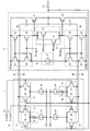
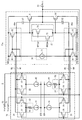
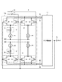
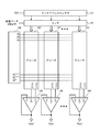
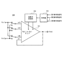
特許文献1に記載のデータドライバ100のブロック図を図9に示す。図9に示すように、データドライバ100は、ラッチアドレスセレクタ181、ラッチ182、参照電圧発生回路186、デコーダ(例えば、D/Aコンバータ)187、出力アンプ188を有する。データドライバ100では、出力アンプ188として内挿アンプを用いる。ここで、出力アンプ188は、入力電圧Vin1、Vin2を1対1で内挿する。つまり、出力アンプ188は、入力電圧Vin1、Vin2が同一電圧のときは出力電圧Voutとして入力電圧Vin1(又は入力電圧Vin2)を出力する。一方、出力アンプ188は、入力電圧Vin1、Vin2が異なるときは入力電圧Vin1と入力電圧Vin2との中間電圧を出力する。内挿機能をもつ出力アンプ備えることで、デコーダ187は、2階調おきの階調電圧に対応する参照電圧(V0、V2、V4、・・・、V2n)から、映像データに応じて同一又は隣り合う2つの参照電圧を選択する構成とすることができる。これにより、デコーダ187が選択する参照電圧数を約半分にすることができるため、デコーダ187の回路規模(素子数)を削減することができる。
A block diagram of the data driver 100 described in
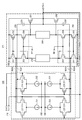
内挿機能をもつ出力アンプ188の回路図を図10に示す。図10に示す出力アンプ188は、特許文献2(特許文献2の図1を帰還型アンプとした構成)を基本構成としている。出力アンプ188は、差動入力部210と、出力増幅部211を有する。差動入力部210は、NMOSトランジスタで構成された2組のNch差動対とPMOSトランジスタで構成された2組のPch差動対を有する。出力増幅部211は、低電圧カスコードカレントミラー250、280、連絡段(浮遊電流源)260、270、出力トランジスタ291、292を有する。
A circuit diagram of the
低電圧カスコードカレントミラー250は、PMOSトランジスタ251〜254により構成され、出力対が共通接続された2組のNch差動対の差動電流出力を受ける。低電圧カスコードカレントミラー280は、NMOSトランジスタ281〜284により構成され、出力対が共通接続された2組のPch差動対の差動電流出力を受ける。連絡段260は、低電圧カスコードカレントミラー250の出力(PMOSトランジスタ254のドレイン)と低電圧カスコードカレントミラー280の出力(NMOSトランジスタ284のドレイン)とを接続する。連絡段270は、低電圧カスコードカレントミラー250の入力(PMOSトランジスタ253のドレイン)と低電圧カスコードカレントミラー280の入力(NMOSトランジスタ283のドレイン)とを接続する。出力トランジスタ291は、ドレインが出力端子に接続され、ゲートが低電圧カスコードカレントミラー250の出力と連絡段260の接続点に接続され、ソースが高電位側電源VDDに接続されたPMOSトランジスタで構成され、出力トランジスタ292は、ドレインが出力端子に接続され、ゲートが低電圧カスコードカレントミラー280の出力と連絡段260の接続点に接続され、ソースが低電位側電源VSSに接続されたNMOSトランジスタで構成される。この出力アンプ188は、差動入力部がNch差動対とPch差動対を有するため、入力電圧が電源付近とされ一方の差動対が停止する場合においてもいずれか一方の差動対が動作し、電源電圧と同じ電圧範囲で出力増幅動作が可能なアンプ(Rail−to−Railアンプと称す)を構成する。
The low voltage cascode
なお、図10に示した出力アンプ188の差動入力部210は、2組のNch差動対((221、222)、(223、224))と、2組のPch差動対((225、226)、(227、228))とで構成される。そして、4つの差動対はそれぞれ、個別の電流源(231、232、233、234)で駆動される。1組目のNch差動対(221、222)とPch差動対(225、226)は、入力対の第1入力端子(トランジスタ221、225のゲート)に入力電圧Vin1が入力され、第2入力端子(トランジスタ222、226のゲート)に出力電圧Voutが入力される。2組目のNch差動対(223、224)とPch差動対(227、228)は、入力対の第1入力端子(トランジスタ223、227のゲート)に入力電圧Vin2が入力され、第2入力端子(トランジスタ224、228のゲート)に出力電圧Voutが入力される。また、Nch差動対(221、222)、(223、224)は出力対がそれぞれ共通接続される。そして、出力対の一方のノードN201がカレントミラー250の出力側ノード(PMOSトランジスタ252、254の接続点)に接続され、出力対の他方のノードN202がカレントミラー250の入力側ノード(PMOSトランジスタ251、253の接続点)に接続される。また、Pch差動対(225、226)、(227、228)も出力対がそれぞれ共通接続される。そして、出力対の一方のノードN203がカレントミラー280の出力側ノード(NMOSトランジスタ282、284の接続ノード)に接続され、出力対の他方のノードN204がカレントミラー280の入力側ノード(NMOSトランジスタ281、283の接続ノード)に接続される。
10 includes two sets of Nch differential pairs ((221, 222), (223, 224)) and two sets of Pch differential pairs ((225). 226), (227, 228)). Each of the four differential pairs is driven by a separate current source (231, 232, 233, 234). In the first pair of Nch differential pair (221, 222) and Pch differential pair (225, 226), the input voltage Vin1 is input to the first input terminal of the input pair (the gates of the
ここでNch差動対(221、222)、(223、224)に着目する。Nch差動対を構成するトランジスタサイズが等しいとすると、NMOSトランジスタ221〜224のドレイン電流I(221)、I(222)、I(223)、I(224)は以下で与えられる。
I(221)=(β/2)(Vin1−Vs1−VTH))^2 ・・・(1)
I(222)=(β/2)(Vout−Vs1−VTH))^2 ・・・(2)
I(223)=(β/2)(Vin2−Vs2−VTH))^2 ・・・(3)
I(224)=(β/2)(Vout−Vs2−VTH))^2 ・・・(4)
ただし、βは利得係数であり、β(=μ(W/L)(εx/tox)、ただしμは電子の実効移動度、εxはゲート絶縁膜の誘電率、toxはゲート絶縁膜の膜厚、Wはチャネル幅、Lはチャネル長)、VTHは閾値電圧、Vs1及びVs2は差動対(221、222)、(223、224)のそれぞれの共通ソース電圧である。
Here, attention is paid to the Nch differential pairs (221, 222) and (223, 224). Assuming that the transistor sizes constituting the Nch differential pair are equal, the drain currents I (221), I (222), I (223), and I (224) of the
I (221) = (β / 2) (Vin1-Vs1-VTH)) ^ 2 (1)
I (222) = (β / 2) (Vout−Vs1−VTH)) ^ 2 (2)
I (223) = (β / 2) (Vin2-Vs2-VTH)) ^ 2 (3)
I (224) = (β / 2) (Vout−Vs2−VTH)) ^ 2 (4)
Where β is a gain coefficient, β (= μ (W / L) (εx / tox), where μ is the effective mobility of electrons, εx is the dielectric constant of the gate insulating film, and tox is the film thickness of the gate insulating film. , W is the channel width, L is the channel length, VTH is the threshold voltage, and Vs1 and Vs2 are the common source voltages of the differential pairs (221, 222) and (223, 224), respectively.
Nch差動対(221、222)、(223、224)の共通出力対の一方のノードN201の出力電流(I(221)+I(223))はカレントミラー250の出力側ノード(PMOSトランジスタ252、254の接続点)を介してカレントミラー250の出力電流に連結され、共通出力対の他方のノードN202の出力電流(I(222)+I(224))はカレントミラー250の入力側ノード(PMOSトランジスタ251、253の接続点)を介してカレントミラー250の入力電流に連結される。出力アンプ188は、カレントミラー250の入力電流と出力電流が等しくなるように出力電圧Voutを制御する。つまり、ドレイン電流I(221)〜I(224)は以下の関係を有する。
I(221)+I(223)=I(222)+I(224) ・・・(5)
The output current (I (221) + I (223)) of one node N201 of the common output pair of the Nch differential pairs (221, 222), (223, 224) is an output side node (
I (221) + I (223) = I (222) + I (224) (5)
また、Nch差動対(221、222)、(223、224)をそれぞれ駆動する電流源231、232の出力電流を同一電流とする。これにより、ドレイン電流I(221)〜I(224)は以下の関係を有する。
I(221)+I(222)=I(223)+I(224) ・・・(6)
Further, the output currents of the
I (221) + I (222) = I (223) + I (224) (6)
そして、式(5)と式(6)より、以下の式(7)と式(8)が導き出される。
I(221)=I(224) ・・・(7)
I(222)=I(223) ・・・(8)
Then, from the equations (5) and (6), the following equations (7) and (8) are derived.
I (221) = I (224) (7)
I (222) = I (223) (8)
ここで式(1)乃至(4)を式(7)及び式(8)に代入し、Vs1、Vs2を消去すると、式(9)が導き出される。
Vout=(Vin1+Vin2)/2 ・・・(9)
Here, when Expressions (1) to (4) are substituted into Expressions (7) and (8) and Vs1 and Vs2 are deleted, Expression (9) is derived.
Vout = (Vin1 + Vin2) / 2 (9)
Pch差動対(225、226)、(227、228)についても、同様の計算を行うことで式(9)と同等の関係式が得られる。すなわち、図10の出力アンプ188は、2つの入力電圧Vin1、Vin2を受け、その中間電圧(内挿電圧)を出力することができる。なお、このような内挿アンプの入出力電圧特性については特許文献3等にも開示されている。
For the Pch differential pairs (225, 226) and (227, 228), a relational expression equivalent to the expression (9) can be obtained by performing the same calculation. That is, the
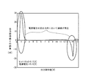
データドライバ100では、図10に示した出力アンプ188を用いることで、多ビット映像データを処理するデコーダ(例えば、D/Aコンバータ)の回路規模の増加を抑制できる。しかし、出力アンプ188には電源電圧近傍の所定の電圧範囲で出力誤差が増加することが特許文献1において指摘されている。特許文献1においてこの課題を示す図として図11のグラフが示されている。図11に示すグラフは、出力アンプ188の2つの入力電圧Vin1、Vin2(Vin1>Vin2)が0.2Vの電圧差を有する場合における出力設定電圧(出力期待値)と出力誤差の定常特性を示している。図11に示す例では、低電位電源電圧側0.5V〜2V付近で出力誤差が正側に増加し、高電位電源電圧側13V〜14.5V付近で出力誤差が負側に増加している。この電源電圧付近の出力誤差の増加は、例えば低電位側電源電圧の近傍で2つの入力電圧Vin1、Vin2が低下すると、2つのNch差動対のうち、低電位の入力電圧Vin2を受けるNch差動対が先に停止し、次いで高電位の入力電圧Vin1を受けるNch差動対が停止するときに生じる。この出力誤差の増加の原因は、それぞれのNch差動対が停止する過程において、差動対を構成するトランジスタのゲート・ソース間電圧が低下してドレイン・ソース間電流が減少し、Nch差動対における上記式(1)乃至(8)の関係が崩れることにある。なお、2つのNch差動対が共に停止すると、2つのPch差動対による作用のみとなり、出力誤差は減少し正常出力となる。同様に、高電位側電源電圧の近傍で2つの入力電圧Vin1、Vin2が上昇すると、2つのPch差動対のうち、高電位の入力電圧Vin1を受けるPch差動対が先に停止し、次いで低電位の入力電圧Vin2を受けるPch差動対が停止するときに出力誤差が増加する。
In the data driver 100, by using the
電源電圧近傍の上記出力誤差は、出力アンプ188の2つの入力電圧Vin1、Vin2の電圧差が大きいほど増大する。出力誤差が増大する電源電圧近傍の電圧範囲では図10のような内挿アンプは高精度な電圧出力ができないという問題がある。
The output error near the power supply voltage increases as the voltage difference between the two input voltages Vin1 and Vin2 of the
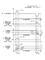
ここで、出力誤差が増大するメカニズムについて、本願発明者らによる分析を以下に示す。図10に示した出力アンプ188において出力誤差が増大するメカニズムを説明するための差動増幅器の出力設定電圧(出力期待値)と出力電圧誤差の定常特性を示すグラフを図12に示す。図12に示す動作例では、図10の出力アンプ188の入力電圧Vin1、Vin2は、Vin1が入力電圧Vin2より電圧差ΔVだけ高い電圧信号に設定されている(Vin1−Vin2=ΔV、ΔV>0)。また、図12に示す動作例では、出力設定電圧は、入力電圧Vin1、Vin2の中間電圧:(Vin1+Vin2)/2)に設定されている。
Here, the analysis by the inventors of the present application will be described below with respect to the mechanism by which the output error increases. FIG. 12 is a graph showing the steady state characteristics of the output setting voltage (output expected value) of the differential amplifier and the output voltage error for explaining the mechanism of the output error increase in the
図10の出力アンプ188のNch差動対(221、222)、(223、224)は、内挿作用が正常に行われるときは、上記式(7)及び(8)の関係を満たしている。入力電圧Vin1が入力電圧Vin2より高電位のとき、電流I(221)、I(224)は、電流I(222)、I(223)より大きい。そして、本動作例では、電流I(221)〜I(224)は、I(221)=I(224)=In2、I(222)=I(223)=In1、In2>In1という関係を有する。なお、合計電流(In1+In2)は電流源231、232のそれぞれが出力する電流の電流値(同一電流値)に対応している。また、Pch差動対(225、226)、(227、228)も同様に、入力電圧Vin1がVin2より高電位で内挿作用が正常に行われるとき、電流I(227)及びI(226)は、電流I(225)及びI(228)より大きい。そして、電流I(225)〜I(228)は、I(227)=I(226)=Ip2、I(225)=I(228)=Ip1、Ip2>Ip1という関係を有する。なお、合計電流(Ip1+Ip2)は電流源233、234のそれぞれが出力する電流の電流値(同一電流値)に対応している。また、Pch差動対の各電流はドレイン・ソース間電流の絶対値で表す。
The Nch differential pairs (221, 222) and (223, 224) of the
図12の(1)は、Nch差動対(221、222)、(223、224)の各トランジスタ111〜114の電流特性を表している。電流I(221)、I(222)は実線、電流I(223)、I(224)は破線で示した。Nch差動対の各トランジスタの電流は、高電位側電源電圧VDDに近い出力設定電圧の範囲において、I(221)=I(224)=In2、I(222)=I(223)=In1という状態で一定に保たれ、内挿作用は正常に行われる。一方、低電位側電源電圧VSSに近い出力設定電圧の範囲では、入力電圧Vin1、Vin2が低下して出力設定電圧が電圧Vdまで低下すると、まず低電位側の入力電圧Vin2を受けるNch差動対(223、224)の共通ソース端子が低電位側電源電圧VSSに達する。そして更に出力設定電圧が低下すると、Nch差動対(223、224)の共通ソース端子は低電位側電源電圧VSSより低下できないので、差動対(223、224)の入力電圧のみが低下(トランジスタ223、224のゲート・ソース間電圧が減少)する。これにより電流I(223)、I(224)は出力設定電圧がVdより低下するに伴って減少を始める。そして出力設定電圧が電圧Vbで電流I(223)、I(224)はほぼゼロとなり、Nch差動対(223、224)は停止する。一方、入力電圧Vin1を受けるNch差動対(221、222)の共通ソース端子は出力設定電圧が電圧Vcで低電位側電源電圧VSSに達する。そして更に出力設定電圧が低下すると、Nch差動対(221、222)の入力電圧のみが低下(トランジスタ221、222のゲート・ソース間電圧が減少)する。これにより電流I(221)、I(222)は出力設定電圧がVcより低下するに伴って減少を始める。そして出力設定電圧が電圧Vaで電流I(221)、I(222)はほぼゼロとなり、Nch差動対(221、222)は停止する。なお、電圧VaとVbの電位差、電圧VcとVdの電位差はΔVに依存し、電圧Vb、Vcの大小は、ΔVやNch差動対のトランジスタ特性により変化する。図12では、Vb<Vcの例を示している。
(1) in FIG. 12 represents current characteristics of the transistors 111 to 114 of the Nch differential pair (221, 222) and (223, 224). The currents I (221) and I (222) are indicated by solid lines, and the currents I (223) and I (224) are indicated by broken lines. The currents of the transistors of the Nch differential pair are I (221) = I (224) = In2 and I (222) = I (223) = In1 in the output set voltage range close to the high potential side power supply voltage VDD. The state is kept constant and the interpolating action is performed normally. On the other hand, in the range of the output setting voltage close to the low potential side power supply voltage VSS, when the input voltages Vin1 and Vin2 decrease and the output setting voltage decreases to the voltage Vd, the Nch differential pair that first receives the low potential side input voltage Vin2. The common source terminal of (223, 224) reaches the low potential side power supply voltage VSS. When the output setting voltage further decreases, the common source terminal of the Nch differential pair (223, 224) cannot be lowered below the low-potential side power supply voltage VSS, so that only the input voltage of the differential pair (223, 224) decreases (
図12の(2)は、差動入力部210のノードN201、N202の出力電流差(I(N201)−I(N202))の特性(特性曲線Isn_ref)を表している。出力電流I(N201)はNch差動対の電流I(221)とI(223)の合計電流、出力電流I(N202)はNch差動対の電流I(222)とI(224)の合計電流である。出力電流I(N201)及び出力電流I(202)は、それぞれ出力増幅部211のカレントミラー250の出力側ノードと入力側ノードの電流に結合されている。出力電流差(I(N201)−I(N202))は、内挿作用が正常に行われる定常特性では通常ゼロとなる。図12の(2)では、出力電流差(I(N201)−I(N202))は、高電位側電源電圧VDDに近い出力設定電圧の範囲ではゼロとなるが、低電位側電源電圧VSSに近い出力設定電圧の範囲においては出力設定電圧が電圧Vd〜Vaの範囲で正側に増加する。この出力電流差(I(N201)−I(N202))の増加の原因は、Nch差動対の各電流の変化に依存する。具体的には、図12の(1)において、出力設定電圧が電圧Vdより低下すると、電流I(223)、I(224)がそれぞれ減少する。このとき電流I(224)の減少量の方が大きく、電流I(221)、I(222)は変化しないため、出力電流I(N201)よりI(N202)の減少量が大きくなり、出力電流差(I(N201)−I(N202))が正側に増加する。出力設定電圧が電圧Vcより低下すると、電流I(223)、I(224)に加えて電流I(221)、I(222)もそれぞれ減少する。このとき、電流I(222)の減少量よりI(221)の減少量の方が大きい。すなわち出力電流差(I(N201)−I(N202))は、電流I(221)、I(222)、I(223)、I(224)の変化に依存し、出力設定電圧がVdからVcまで正側に増加し、VcからVbまで増加量がピークとなり、VbからVaでは減少し、VaからVSSではゼロに戻る。
(2) in FIG. 12 represents the characteristic (characteristic curve Isn_ref) of the output current difference (I (N201) −I (N202)) between the nodes N201 and N202 of the
図12の(2)の差動入力部210のノードN201、N202の出力電流差(I(N201)−I(N202))の特性(特性曲線Isn_ref)の正側への増加は図12の(5)の出力電圧誤差の特性(特性曲線Ve_ref)に影響を与える。これは例えば、差動入力部210の入力電圧Vin1、Vin2が出力電圧Voutより高電位側に変化したときのNch差動対(221、222)、(223、224)の応答作用から容易に理解できる。入力電圧Vin1、Vin2が出力電圧Voutより高電位側に変化すると、Nch差動対(221、222)、(223、224)の電流I(221)、I(223)が増加し、電流I(222)、I(224)は減少する。これはすなわち出力電流I(N201)が増加し、出力電流I(N202)が減少する作用である。これにより出力増幅部211が作用して出力電圧Voutが高電位側へ変化する。図11の(2)では、出力設定電圧が電圧Vd〜Vaで出力電流差(I(N201)−I(N202))が正側に増加している。このため、図11の(5)において、出力電圧Voutは、出力電流差(I(N201)−I(N202))の正側への増加に応じて高電位側への変動作用を受けるため、高電位側(正側)へ出力誤差が発生する。
Node N201, an output current difference N202 of the differential input section 210 (2) of FIG. 12 (I (N201) -I (N202)) of the characteristic increase in the positive side of the (characteristic curve Isn_ref) of FIG. 12 ( 5) The output voltage error characteristic (characteristic curve Ve_ref) is affected. This can be easily understood from, for example, the response action of the Nch differential pairs (221, 222) and (223, 224) when the input voltages Vin1 and Vin2 of the
図12の(3)は、Pch差動対(225、226)、(227、228)の各トランジスタ225〜228の電流特性を表している。電流I(227)、I(228)は実線、電流I(225)、I(226)は破線で示す。各電流は各トランジスタのドレイン・ソース間電流の絶対値とする。Pch差動対の各トランジスタの電流は低電位側電源電圧VSS側ではI(225)、I(228)はIp1、I(226)、I(227)はIp2で一定に保たれ、内挿作用は正常に行われる。一方、高電位側電源電圧VDD側の出力設定電圧の範囲では、入力電圧Vin1、Vin2が上昇して出力設定電圧が電圧Veまで上昇すると、まず高電位の入力電圧Vin1を受けるPch差動対(225、226)の共通ソース端子が電源電圧VDDに達する。そして更に出力設定電圧が上昇すると、Pch差動対(225、226)の共通ソース端子は電源電圧VDDより上昇できないので、差動対(225、226)の入力電圧のみが上昇(トランジスタ225、226のゲート・ソース間電圧の絶対値が減少)する。これにより電流I(225)、I(226)は出力設定電圧がVeより上昇するに伴って減少を始める。そして出力設定電圧が電圧Vgで電流I(225)、I(226)はほぼゼロとなり、Pch差動対(225、226)は停止する。一方、入力電圧Vin2を受けるPch差動対(227、228)の共通ソース端子は出力設定電圧が電圧Vfで高電位側電源電圧VDDに達する。そして更に出力設定電圧が上昇すると、Pch差動対(227、228)のトランジスタ227、228のゲート・ソース間電圧の絶対値が減少する。これにより電流I(227)、I(228)は出力設定電圧が電圧Vfより上昇するに伴って減少を始める。そして出力設定電圧が電圧Vhで電流I(227)、I(228)はほぼゼロとなり、Pch差動対(227、228)は停止する。
(3) in FIG. 12 represents current characteristics of the
図12の(4)は、差動入力部210のノードN203、N204の出力電流差(I(N203)−I(N204))の特性(特性曲線Isp_ref)を表している。出力電流I(N203)はPch差動対の電流I(225)とI(227)の合計電流、出力電流I(N204)はPch差動対の電流I(226)とI(228)の合計電流である。出力電流I(N203)及び出力電流I(N204)は、それぞれ出力増幅部211のカレントミラー280の出力側ノードと入力側ノードの電流に結合されている。出力電流差(I(N203)−I(N204))は、内挿作用が正常に行われる定常特性では通常ゼロとなる。図12の(4)では、出力電流差(I(N203)−I(N204))は、低電位側電源電圧VSSに近い出力設定電圧の範囲ではゼロとなるが、高電位側電源電圧VDDに近い出力設定電圧の範囲において出力設定電圧が電圧Ve〜Vhの範囲では正側に増加する。この出力電流差(I(N203)−I(N204))の増加の原因は、Pch差動対の各電流の変化に依存する。すなわち出力電流差(I(N203)−I(N204))は、図12の(3)の電流I(225)、I(226)、I(227)、I(228)の変化に依存し、出力設定電圧がVeからVfまで正側に増加し、VfからVgまで増加量がピークとなり、VgからVhでは減少し、VhからVDDではゼロに戻る。
(4) in FIG. 12 represents the characteristic (characteristic curve Isp_ref) of the output current difference (I (N203) −I (N204)) between the nodes N203 and N204 of the
図12の(4)の差動入力部210のノードN203、N204の出力電流差(I(N203)−I(N204))の特性(特性曲線Isp_ref)は図12の(5)の出力電圧誤差の特性(特性曲線Ve_ref)に影響を与える。これは例えば、差動入力部210の入力電圧Vin1、Vin2が出力電圧Voutより低電位側に変化したときのPch差動対(225、226)、(227、228)の応答作用から容易に理解できる。入力電圧Vin1、Vin2が出力電圧Voutより低電位側に変化すると、Pch差動対(225、226)、(227、228)の電流I(225)、I(227)が増加し、電流I(226)、I(228)は減少する。これはすなわち出力電流差I(N203)が増加し、出力電流差I(N204)が減少する作用である。これにより出力増幅部211が作用して出力電圧Voutが低電位側へ変化する。すなわち、図12の(4)では、出力設定電圧が電圧Ve〜Vhで出力電流差(I(N203)−I(N204))が正側に増加している。このため、図12の(5)において、出力電圧Voutは、出力電流差(I(N203)−I(N204))の正側への増加に応じて低電位側への変動作用を受けるため、低電位側(負側)へ出力誤差が発生する。
The characteristic (characteristic curve Isp_ref) of the output current difference (I (N203) -I (N204)) of the nodes N203 and N204 of the
以上、図14の内挿アンプにおける出力誤差増大のメカニズムを説明した。すなわち図10の出力アンプ188における電源電圧近傍の出力誤差は、定常特性において差動入力部210のNch差動側の出力電流差(I(N201)−I(N202))及びPch差動側の出力電流差(I(N203)−I(N204))の増加に対応して発生する。そして図12の(5)の出力電圧Voutの出力誤差の定常特性は、図11の出力誤差の定常特性と合致している。
The mechanism for increasing the output error in the interpolation amplifier of FIG. 14 has been described above. That is, the output error in the vicinity of the power supply voltage in the
そこで、特許文献1では、出力誤差の増大を防止する技術が提案されている。特許文献1に開示される出力アンプ300のブロック図を図13に示す。図13に示す出力アンプ300は、内挿アンプ301、判別部302、差動対制御部303を有する。判別部302は、出力電圧Vout等を被判別信号として、出力電圧が内挿アンプの出力誤差が増大する電圧範囲を含むか否かを判別して判別信号を出力する。差動対制御部303は、判別信号により、出力電圧Voutが内挿アンプの出力誤差が増大する電圧範囲に含まれるという判別結果を示すときに差動対を停止させる。差動対制御部303は、具体的には図14に示すように、差動対を駆動する電流源を停止させる。例えば、低電位側電源電圧近傍の出力誤差が増大する電圧範囲では、差動対制御部303により2つのNch差動対を駆動する電流源331、332を非活性(停止)とする。また、高電位側電源電圧近傍の出力誤差が増大する電圧範囲では、差動対制御部303により2つのPch差動対を駆動する電流源333、334を非活性(停止)とする。これにより、電源電圧近傍では出力誤差増大の作用を生じるNch又はPch差動対が停止され、出力誤差の増大を防止できる。
Therefore, in
しかしながら、特許文献1に記載の内挿アンプでは、各差動対を駆動する電流源の活性、非活性を制御するために、差動対の数に対応した数のスイッチ(例えば、図14では4個のスイッチ)が少なくとも必要とされる。更に、判別部302としてコンパレータ等の回路が必要とされる。このため、内挿アンプ1個あたりに追加される素子数が多く、内挿アンプの面積が増加するという問題がある。
However, in the interpolation amplifier described in
本発明にかかる差動増幅器は、第1の入力電圧(Vin1)と第2の入力電圧(Vin2)との間の信号レベルを有する出力電圧(Vout)を出力する差動増幅器であって、前記第1の入力電圧及び前記第2の入力電圧の一方と前記出力電圧(Vout)との差に基づき第1の電流ノード対(N1、N2)に第1の差動電流を出力し、第1導電型トランジスタで形成される第1の差動対(31、32)と、前記第1の入力電圧及び前記第2の入力電圧の他方と前記出力電圧との差に基づき前記第1の電流ノード対(N1、N2)に第2の差動電流を出力し、前記第1導電型トランジスタで形成される第2の差動対(33、34)と、前記第1の入力電圧及び前記第2の入力電圧の前記一方と前記出力電圧との差に基づき第2の電流ノード対(N3、N4)に第3の差動電流を出力し、第2導電型トランジスタで形成される第3の差動対(35、36)と、前記第1の入力電圧及び前記第2の入力電圧の前記他方と前記出力電圧との差に基づき前記第2の電流ノード対(N3、N4)に第4の差動電流を出力し、前記第2導電型トランジスタで形成される第4の差動対(37、38)と、第1の電源電圧(VSS)を供給する第1の電源と前記第1の差動対(31、32)との間に設けられ、前記第1の差動対に動作電流を供給する第1の電流源(41)と、前記第1の電源と前記第2の差動対(33、34)との間に設けられ、前記第2の差動対に動作電流を供給する第2の電流源(42)と、第2の電源電圧(VDD)を供給する第2の電源と前記第3の差動対(35、36)との間に設けられ、前記第3の差動対に動作電流を供給する第3の電流源(43)と、前記第2の電源と前記第4の差動対(37、38)との間に設けられ、前記第4の差動対に動作電流を供給する第4の電流源(44)と、前記第1、第2の入力電圧と前記出力電圧に基づき前記第1の差動対(31、32)及び前記第2の差動対(33、34)にそれぞれ流れる電流量が前記第1の電流源(41)及び前記第2の電流源(42)により設定される動作電流よりも小さくなる第1の動作範囲において、前記第1の差動対に供給される動作電流の変化点を制御する第1の制御回路(51)と、前記第1、第2の入力電圧と前記出力電圧に基づき前記第3の差動対(35、36)及び前記第4の差動対(37、38)にそれぞれ流れる電流量が前記第3の電流源(43)及び前記第4の電流源(44)により設定される動作電流よりも小さくなる第2の動作範囲において、前記第3の差動対又は前記第4の差動対に供給される動作電流の変化点を制御する第2の制御回路(52)と、前記第1の電流ノード対(N1、N2)から出力される前記第1及び第2の差動電流を合成した差動電流出力と、前記第2の電流ノード対(N3、N4)から出力される前記第3及び第4の差動電流を合成した差動電流出力と、に基づき前記出力電圧(Vout)を生成する出力増幅部(11)と、を有する。 A differential amplifier according to the present invention is a differential amplifier that outputs an output voltage (Vout) having a signal level between a first input voltage (Vin1) and a second input voltage (Vin2), Based on the difference between one of the first input voltage and the second input voltage and the output voltage (Vout), a first differential current is output to the first current node pair (N1, N2), The first current node based on a difference between the first differential pair (31, 32) formed of a conductive transistor and the other of the first input voltage and the second input voltage and the output voltage A second differential current is output to the pair (N1, N2), the second differential pair (33, 34) formed by the first conductivity type transistor, the first input voltage, and the second A second current node pair based on the difference between the one of the input voltages and the output voltage N3, N4) outputs a third differential current, a third differential pair (35, 36) formed of a second conductivity type transistor, the first input voltage and the second input voltage A fourth differential current formed by the second conductivity type transistor by outputting a fourth differential current to the second current node pair (N3, N4) based on the difference between the other of the second and the output voltage. The first differential pair is provided between a pair (37, 38), a first power supply for supplying a first power supply voltage (VSS), and the first differential pair (31, 32). A first current source (41) for supplying an operating current to the first power source, and provided between the first power source and the second differential pair (33, 34), and operates on the second differential pair. A second current source (42) for supplying a current; a second power source for supplying a second power supply voltage (VDD); and the third differential pair (35, 36). Between a third current source (43) for supplying an operating current to the third differential pair, and between the second power source and the fourth differential pair (37, 38). A fourth current source (44) for supplying an operating current to the fourth differential pair, and the first differential pair (based on the first and second input voltages and the output voltage). 31 and 32) and the second differential pair (33 and 34), the amount of current flowing through each of them is larger than the operating current set by the first current source (41) and the second current source (42) A first control circuit (51) for controlling a change point of the operating current supplied to the first differential pair in the first operating range to be reduced, the first and second input voltages, and the output Based on the voltage, the amount of current flowing through each of the third differential pair (35, 36) and the fourth differential pair (37, 38) In the second operating range that is smaller than the operating current set by the third current source (43) and the fourth current source (44), the third differential pair or the fourth differential A second control circuit (52) for controlling a change point of an operating current supplied to the pair, and the first and second differential currents output from the first current node pair (N1, N2). Based on the synthesized differential current output and the differential current output synthesized from the third and fourth differential currents output from the second current node pair (N3, N4), the output voltage (Vout And an output amplifying unit (11) for generating
本発明にかかる差動増幅器では、出力誤差が増大する第1の動作範囲及び第2の動作範囲において、第1、第2の制御回路が出力誤差の原因となる第1及び第2の出力ノード対の差動電流出力の電流差の増加を抑制する。つまり、本発明にかかる差動増幅器では、第1、第2の制御回路により、第1の動作範囲及び第2の動作範囲において、第1の入力電圧と第2の入力電圧のうち最寄りの電源電圧との電圧差が大きい入力電圧を受ける差動対に供給される電流源からの動作電流の変化点を制御することで、第1及び第2の出力ノード対の差動電流出力の電流差の増加を抑制して出力誤差の増大を防止することができる。また、本発明にかかる差動増幅器では、第1、第2の制御回路は、素子数の少ない単純回路で構成できるため小面積で実現できる。 In the differential amplifier according to the present invention, the first and second output nodes causing the output error by the first and second control circuits in the first operating range and the second operating range in which the output error increases. Suppresses the increase in current difference between the pair of differential current outputs. In other words, in the differential amplifier according to the present invention, the first and second control circuits allow the nearest power source among the first input voltage and the second input voltage in the first operation range and the second operation range. By controlling the change point of the operating current from the current source supplied to the differential pair receiving the input voltage having a large voltage difference from the voltage, the current difference between the differential current outputs of the first and second output node pairs The increase in output error can be suppressed and the increase in output error can be prevented. In the differential amplifier according to the present invention, the first and second control circuits can be realized with a small area because they can be configured by a simple circuit having a small number of elements.
本発明にかかる差動増幅器では、回路規模の増大を抑制しながら、出力誤差の増大を防止することができる。 In the differential amplifier according to the present invention, an increase in output error can be prevented while suppressing an increase in circuit scale.
実施の形態1
以下、図面を参照して本発明の実施の形態について説明する。本実施の形態にかかる差動増幅器は、2つの入力電圧を1対1で内挿した内挿電圧を出力する内挿アンプである。つまり、本実施の形態にかかる差動増幅器は、データドライバ等に用いることでD/Aコンバータ等の素子数を削減することができる。
Embodiments of the present invention will be described below with reference to the drawings. The differential amplifier according to the present embodiment is an interpolation amplifier that outputs an interpolation voltage obtained by interpolating two input voltages on a one-to-one basis. That is, the differential amplifier according to the present embodiment can be used for a data driver or the like to reduce the number of elements such as a D / A converter.
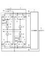
本実施の形態にかかる差動増幅器1の回路図を図1に示す。図1に示すように、差動増幅器1は、差動入力部10と、出力増幅部11を有する。差動入力部10は、入力端子T1、T2に供給される2つの入力電圧Vin1、Vin2と、出力端子T3から出力される出力電圧Voutとの差に基づき差動電流を出力する。出力増幅部11は、差動電流出力に応じて出力電圧Voutを生成する。また、差動増幅器1は、出力増幅部11が生成した出力電圧Voutを差動入力部10に帰還する負帰還構成を有する。また、差動増幅器1に入力される入力電圧Vin1、Vin2は、入力電圧Vin1が入力電圧Vin2よりも高くなるか、又は、入力電圧Vin1、Vin2が同一電圧となるような電圧関係を有する。
A circuit diagram of the
差動入力部10は、第1の差動対21〜第4の差動対24、第1の電流源41〜第4の電流源44、第1の制御回路51、第2の制御回路52を有する。第1の差動対21〜第4の差動対24には、入力電圧Vin1と入力電圧Vin2とのいずれの電圧も入力されうる。しかし、以下の説明では、入力電圧Vin1が第1の差動対21及び第3の差動対23に入力され、入力電圧Vin2が第2の差動対22及び第4の差動対24に入力されるものとする。
The
第1の差動対21は、入力電圧Vin1と出力電圧Voutとの差に基づき第1の電流ノード対に第1の差動電流を出力する。図1では、第1の電流ノード対は、電流ノードN1及び電流ノードN2により構成される。また、第1の差動対21には、第1導電型トランジスタ(例えば、N型のMOSトランジスタ)で形成される。図1に示す例では、第1の差動対21は、第1の差動入力トランジスタ(例えば、NMOSトランジスタ31)、第2の差動入力トランジスタ(例えば、NMOSトランジスタ32)を有する。そして、NMOSトランジスタ31、32の第1端子(例えば、ソース)は共通接続される。NMOSトランジスタ31の制御端子(例えば、ゲート)には、入力電圧Vin1が与えられる。NMOSトランジスタ32の制御端子には、出力電圧Voutが与えられる。NMOSトランジスタ31の第2端子(例えば、ドレイン)は、電流ノードN1に接続される。NMOSトランジスタ32の第2端子は、電流ノードN2に接続される。なお、NMOSトランジスタ31に流れる電流をI(31)で表し、NMOSトランジスタ32に流れる電流をI(32)で表した場合、第1の差動電流は、電流I(31)と電流I(32)とを含む。
The first
第1の電流源41は、第1の電源電圧(例えば、低電位側電源電圧VSS)を供給する第1の電源(低電位側電源)と第1の差動対21との間に設けられる。そして、第1の電流源41は、第1の差動対21に動作電流を供給する。
The first
第2の差動対22は、入力電圧Vin2と出力電圧Voutとの差に基づき第1の電流ノード対(N1、N2)に第2の差動電流を出力する。第2の差動対22には、第1導電型トランジスタ(例えば、N型のMOSトランジスタ)で形成される。図1に示す例では、第2の差動対22は、第3の差動入力トランジスタ(例えば、NMOSトランジスタ33)、第4の差動入力トランジスタ(例えば、NMOSトランジスタ34)を有する。そして、NMOSトランジスタ33、34の第1端子(例えば、ソース)は共通接続される。NMOSトランジスタ33の制御端子(例えば、ゲート)には、入力電圧Vin2が与えられる。NMOSトランジスタ34の制御端子には、出力電圧Voutが与えられる。NMOSトランジスタ33の第2端子(例えば、ドレイン)は、電流ノードN1に接続される。NMOSトランジスタ34の第2端子は、電流ノードN2に接続される。なお、NMOSトランジスタ33に流れる電流をI(33)で表し、NMOSトランジスタ34に流れる電流をI(34)で表した場合、第2の差動電流は、電流I(33)と電流I(34)とを含む。
The second
第2の電流源42は、第1の電源電圧(例えば、低電位側電源電圧VSS)を供給する第1の電源(低電位側電源)と第2の差動対22との間に設けられる。そして、第2の電流源42は、第2の差動対22に動作電流を供給する。
The second
ここで、第1の差動対21が出力する第1の差動電流と第2の差動対22が出力する第2の差動電流は、第1の電流ノード対(N1、N2)において合成される。つまり、電流ノードN1には電流I(31)と電流I(33)を合成した第1の出力電流I(N1)(=I(31)+I(33))が生成され、電流ノードN2には電流I(32)と電流I(34)を合成した第2の出力電流I(N2)(=I(32)+I(34))が生成される。第1の出力電流I(N1)と第2の出力電流I(N2)は、差動入力部10のNch差動対側の第1の電流ノード対(N1、N2)における差動電流出力をなしている。
Here, the first differential current output from the first
第3の差動対23は、入力電圧Vin1と出力電圧Voutとの差に基づき第2の電流ノード対に第3の差動電流を出力する。図1に示す例では、第2の電流ノード対は、電流ノードN3及び電流ノードN4により構成される。また、第3の差動対23には、第2導電型トランジスタ(例えば、P型のMOSトランジスタ)で形成される。図1に示す例では、第3の差動対23は、第5の差動入力トランジスタ(例えば、PMOSトランジスタ35)、第6の差動入力トランジスタ(例えば、PMOSトランジスタ36)を有する。そして、PMOSトランジスタ35、36の第1端子(例えば、ソース)は共通接続される。PMOSトランジスタ35の制御端子(例えば、ゲート)には、入力電圧Vin1が与えられる。PMOSトランジスタ36の制御端子には、出力電圧Voutが与えられる。PMOSトランジスタ35の第2端子(例えば、ドレイン)は、電流ノードN3に接続される。PMOSトランジスタ36の第2端子は、電流ノードN4に接続される。なお、PMOSトランジスタ35に流れる電流をI(35)で表し、PMOSトランジスタ36に流れる電流をI(36)で表した場合、第3の差動電流は、電流I(35)と電流I(36)とを含む。
The third
第3の電流源43は、第2の電源電圧(例えば、高電位側電源電圧VDD)を供給する第2の電源(高電位側電源)と第3の差動対23との間に設けられる。そして、第3の電流源43は、第3の差動対23に動作電流を供給する。
The third
第4の差動対24は、入力電圧Vin2と出力電圧Voutとの差に基づき第2の電流ノード対(N3、N4)に第4の差動電流を出力する。第4の差動対24には、第2導電型トランジスタ(例えば、P型のMOSトランジスタ)で形成される。図1に示す例では、第4の差動対24は、第7の差動入力トランジスタ(例えば、PMOSトランジスタ37)、第8の差動入力トランジスタ(例えば、PMOSトランジスタ38)を有する。そして、PMOSトランジスタ37、38の第1端子(例えば、ソース)は共通接続される。PMOSトランジスタ37の制御端子(例えば、ゲート)には、入力電圧Vin2が与えられる。PMOSトランジスタ38の制御端子には、出力電圧Voutが与えられる。PMOSトランジスタ37の第2端子(例えば、ドレイン)は、電流ノードN3に接続される。PMOSトランジスタ38の第2端子は、電流ノードN4に接続される。なお、PMOSトランジスタ37に流れる電流をI(37)で表し、PMOSトランジスタ38に流れる電流をI(38)で表した場合、第4の差動電流は、電流I(37)と電流I(38)とを含む。
The fourth
第4の電流源44は、第2の電源電圧(例えば、高電位側電源電圧VDD)を供給する第2の電源(高電位側電源)と第4の差動対24との間に設けられる。そして、第4の電流源44は、第4の差動対24に動作電流を供給する。
The fourth
ここで、第3の差動対23が出力する第3の差動電流と第4の差動対24が出力する第4の差動電流は、第2の電流ノード対(N3、N4)において合成される。つまり、電流ノードN3には電流I(35)と電流I(37)を合成した第3の出力電流I(N3)(=I(35)+I(37))が生成され、電流ノードN4には電流I(36)と電流I(38)を合成した第4の出力電流I(N4)(=I(36)+I(38))が生成される。第3の出力電流I(N3)と第4の出力電流I(N4)は、差動入力部10のPch差動対側の第2の電流ノード対(N3、N4)における差動電流出力をなしている。
Here, the third differential current output from the third
第1の制御回路51は、入力電圧Vin1、Vin2がVin1≧Vin2であるとき、電圧Vin1、Vin2のうち第1の電源電圧(低電位側電源電圧VSS)との電圧差が大きい電圧Vin1が入力される第1の差動対21と第1の電流源41との間に設けられる。そして、第1の制御回路51は、入力電圧Vin1、Vin2と出力電圧Voutに基づき第1の差動対21及び第2の差動対22のそれぞれに流れる電流量が第1の電流源41及び第2の電流源42により設定される動作電流よりも小さくなる第1の動作範囲において、第1の差動対21に供給される動作電流の変化点を制御する。本実施の形態では、第1の制御回路51として抵抗R1を用いる。抵抗R1は、入力電圧Vin1がVin2より電圧差ΔVだけ高電位とされた差動増幅器1の定常特性において、入力電圧Vin1、Vin2の低下に伴い、低電位の入力電圧Vin2を受ける第2の差動対22のトランジスタ対の電流(I(33)+I(34))が電流源42で設定された電流より減少し始める変化点に、高電位の入力電圧Vin1を受ける第1の差動対21のトランジスタ対の電流(I(31)+I(32))が電流源41で設定された電流より減少を始める変化点を近づけるような抵抗値に設定される。
When the input voltages Vin1 and Vin2 are Vin1 ≧ Vin2, the
第2の制御回路52は、入力電圧Vin1、Vin2がVin1≧Vin2であるとき、電圧Vin1、Vin2のうち第2の電源電圧(高電位側電源電圧VDD)との電圧差が大きい電圧Vin2が入力される第4の差動対24と第4の電流源44との間に設けられる。そして、第2の制御回路52は、入力電圧Vin1、Vin2と出力電圧Voutに基づき第3の差動対23及び第4の差動対24にそれぞれ流れる電流量が第3の電流源43及び第4の電流源44により設定される動作電流よりも小さくなる第2の動作範囲において、第4の差動対24に供給される動作電流の変化点を制御する。本実施の形態では、第2の制御回路52として抵抗R2を用いる。抵抗R2は、入力電圧Vin1、Vin2の上昇に伴い、高電位の入力電圧Vin1を受ける第3の差動対23のトランジスタ対の電流(I(35)+I(36))が電流源43で設定された電流より減少し始める変化点に、低電位の入力電圧Vin2を受ける第4の差動対24のトランジスタ対の電流(I(37)+I(38))が電流源44で設定された電流より減少を始める変化点を近づけるような抵抗値に設定される。
When the input voltages Vin1 and Vin2 are Vin1 ≧ Vin2, the
出力増幅部11は、第1のカレントミラー60、第1の連絡回路70、第2の連絡回路72、第2のカレントミラー80を有する。
The
第1のカレントミラー60は、第2の電源(例えば、高電位側電源)に接続される第2導電型の第1のトランジスタ対を有し、第1のトランジスタ対に第1の電流ノード対が接続される。また、第1のカレントミラー60は、第2導電型のトランジスタで構成される第3のトランジスタ対を有する。ここで、第1のトランジスタ対は、第1のミラートランジスタ(例えば、PMOSトランジスタ61)と第2のミラートランジスタ(例えば、PMOトランジスタ62)を有する。第3のトランジスタ対は、第3のミラートランジスタ(例えば、PMOSトランジスタ63)、第4のミラートランジスタ(例えば、PMOSトランジスタ64)を有する。
The first
PMOSトランジスタ61、62は、第1端子(例えば、ソース)が高電位側電源に共通に接続され、制御端子(例えば、ゲート)が共通接続される。第1の電流ノード対(N1、N2)の一方のノード(例えば、電流ノードN1)は、PMOSトランジスタ62の第2端子(例えば、ドレイン)に接続され、第1の電流ノード対(N1、N2)の他方のノード(例えば、電流ノードN2)は、PMOSトランジスタ61の第2端子(例えば、ドレイン)に接続される。
The
PMOSトランジスタ63は、第1端子(例えば、ソース)がPMOSトランジスタ61の第2端子(例えば、ドレイン)に接続される。PMOSトランジスタ64は、第1端子(例えば、ソース)がPMOSトランジスタ62の第2端子(例えば、ドレイン)に接続され、制御端子(例えば、ゲート)がPMOSトランジスタ63のゲートと接続される。PMOSトランジスタ63、64のゲートには第1のバイアス電圧BP1が印加される。PMOSトランジスタ63のドレインは、第1のカレントミラー60の入力ノードとなっており、PMOSトランジスタ61、62の共通ゲートと接続される。PMOSトランジスタ64のドレインは、第1のカレントミラー60の出力ノードとなっている。
The
第2のカレントミラー80は、第1の電源(例えば、低電位側電源)に接続される第1導電型の第2のトランジスタ対を有し、第2のトランジスタ対に第2の電流ノード対(N3、N4)が接続される。また、第2のカレントミラー80は、第1導電型のトランジスタで構成される第4のトランジスタ対を有する。ここで、第2のトランジスタ対は、第5のミラートランジスタ(例えば、NMOSトランジスタ81)と第6のミラートランジスタ(例えば、NMOトランジスタ82)を有する。第4のトランジスタ対は、第7のミラートランジスタ(例えば、NMOSトランジスタ83)、第8のミラートランジスタ(例えば、NMOSトランジスタ84)を有する。
The second
NMOSトランジスタ81、82は、第1端子(例えば、ソース)が低電位側電源に共通に接続され、制御端子(例えば、ゲート)が共通接続される。第2の電流ノード対(N3、N4)の一方のノード(例えば、電流ノードN3)は、NMOSトランジスタ82の第2端子(例えば、ドレイン)に接続され、第2の電流ノード対(N3、N4)の他方のノード(例えば、電流ノードN4)は、PMOSトランジスタ81の第2端子(例えば、ドレイン)に接続される。
The
NMOSトランジスタ83は、第1端子(例えば、ソース)がNMOSトランジスタ81の第2端子(例えば、ドレイン)に接続される。NMOSトランジスタ84は、第1端子(例えば、ソース)がNMOSトランジスタ82の第2端子(例えば、ドレイン)に接続され、制御端子(例えば、ゲート)がNMOSトランジスタ83のゲートと接続される。NMOSトランジスタ83、84の共通ゲートには第2のバイアス電圧BN1が印加される。NMOSトランジスタ83のドレインは、第2のカレントミラー80の入力ノードとなっており、NMOSトランジスタ81、82の共通ゲートと接続される。NMOSトランジスタ84のドレインは、第2のカレントミラー80の出力ノードとなっている。
The
第1の連絡回路70は、第1のカレントミラー60の入力ノード(PMOSトランジスタ63のドレイン)と第2のカレントミラー80の入力ノード(NMOSトランジスタ83のドレイン)との間に接続される。第1の連絡回路70は、電流源71を有する。第2の連絡回路72は、第1のカレントミラー60の出力ノード(PMOSトランジスタ64のドレイン)と第2のカレントミラー80の出力ノード(NMOSトランジスタ84のドレイン)との間に接続される。第2の連絡回路72は、互いに並列に接続される第1導電型の第1のフローティングトランジスタ(例えば、NMOSトランジスタ73)と第2導電型の第2フローティングトランジスタ(例えば、PMOSトランジスタ74)を有する。そして、NMOSトランジスタ73の制御端子(例えば、ゲート)には、第3のバイアス電圧BN2が与えられる。PMOSトランジスタ74の制御端子(例えば、ゲート)には第4のバイアス電圧BP2が与えられる。
The
第1の出力トランジスタは、第2導電型のトランジスタ(例えば、PMOSトランジスタ91)である。PMOSトランジスタ91は、出力電圧Voutが出力される出力端子T3と第2の電源(例えば、高電位側電源)との間に接続され、制御端子(例えば、ゲート)が第1のカレントミラー60の出力ノードと第2の連絡回路72の一端との接続点に接続される。
The first output transistor is a second conductivity type transistor (for example, PMOS transistor 91). The
第2の出力トランジスタは、第1導電型のトランジスタ(例えば、NMOSトランジスタ92)である。NMOSトランジスタ92は、出力電圧Voutが出力される出力端子T3と第1の電源(例えば、低電位側電源)との間に接続され、制御端子(例えば、ゲート)が第2のカレントミラー80の出力ノードと第2の連絡回路72の他端との接続点に接続される。
The second output transistor is a first conductivity type transistor (for example, NMOS transistor 92). The
さらに、差動増幅器1は、コンデンサC1、C2を有する。コンデンサC1、C2は位相補償用コンデンサである。コンデンサC1は、出力端子T3と電流ノードN1との間に接続される。コンデンサC2は、出力端子T3と電流ノードN3との間に接続される。
Further, the
続いて、実施の形態1にかかる差動増幅器1の動作について説明する。なお、以下の説明では、差動増幅器1の出力電圧の期待値(以下、出力設定電圧値と称す)として入力電圧Vin1、Vin2の中間電圧((Vin1+Vin2)/2)を設定する。なお、入力電圧Vin1、Vin2の電位差ΔV(=Vin1−Vin2)を用いると、入力電圧Vin1は出力設定電圧よりもΔV/2だけ高い電圧、入力電圧Vin2は出力設定電圧よりΔV/2だけ低い電圧となる。また、以下の説明では、NMOSトランジスタ31〜34に流れる電流をI(31)〜I(34)で表し、PMOSトランジスタ35〜38に流れる電流の絶対値をI(35)〜I(38)で表す。
Next, the operation of the
また、各実施の形態の説明では、第1の動作範囲と第2の動作範囲は、差動増幅器の定常特性に出力設定電圧に対して定義される。第1の動作範囲は、入力電圧Vin1、Vin2と出力電圧Voutとの電圧差に基づき第1の差動対21及び第2の差動対22にそれぞれ流れる電流量が第1の電流源41及び第2の電流源42により設定される動作電流よりも小さくなる出力設定電圧の範囲である。より具体的には、入力電圧Vin1、Vin2が低下して低電位側電源電圧VSSに近づくと、第1の差動対21及び第2の差動対22の共通ソース端子の電圧が低下して、低電位側電源電圧VSSに到達する。更に入力電圧Vin1、Vin2が低下した場合、第1の差動対21及び第2の差動対22の共通ソース端子の電圧は低電位側電源電圧VSSより低下できないため、差動対を構成するトランジスタのゲート・ソース間電圧が低下して、差動対に流れる電流が対応する電流源で設定された電流値から減少する。更に入力電圧Vin1、Vin2が低下すると、第1の差動対21及び第2の差動対22のトランジスタ対はオフとなる。ここで、第1の差動対21のトランジスタ対の電流(NMOSトランジスタ31、32のドレイン・ソース間電流の合計)、及び、第2の差動対21のトランジスタ対の電流(NMOSトランジスタ33、34のドレイン・ソース間電流の合計)のうち少なくとも一方がそれぞれ対応する電流源で設定された電流値から減少しているか、又は第1の差動対21及び第2の差動対22のトランジスタ対がオフしている出力設定電圧の電圧範囲を第1の動作範囲と定義する。
In the description of each embodiment, the first operating range and the second operating range are defined with respect to the output set voltage in the steady-state characteristics of the differential amplifier. The first operating range is that the amount of current flowing through the first
また、第2の動作範囲は、入力電圧Vin1、Vin2と出力電圧Voutに基づき第3の差動対23及び第4の差動対24にそれぞれ流れる電流量が第3の電流源43及び第4の電流源44により設定される動作電流よりも小さくなる出力設定電圧の範囲である。より具体的には、入力電圧Vin1、Vin2が上昇して高電位側電源電圧VDDに近づくと、第3の差動対23及び第4の差動対24の共通ソース端子の電圧が上昇して、高電位側電源電圧VDDに到達する。更に入力電圧Vin1、Vin2が上昇した場合、第3の差動対23及び第4の差動対24の共通ソース端子の電圧は高電位側電源電圧VDDより上昇できないため、差動対を構成するトランジスタのゲート・ソース間電圧が低下して、差動対に流れる電流が対応する電流源で設定された電流値から減少する。更に入力電圧Vin1、Vin2が上昇すると、第3の差動対23及び第4の差動対24のトランジスタ対はオフとなる。ここで、第3の差動対23のトランジスタ対の電流(PMOSトランジスタ35、36のドレイン・ソース間電流の合計)、及び、第4の差動対24のトランジスタ対の電流(PMOSトランジスタ37、38のドレイン・ソース間電流の合計)のうち少なくとも一方がそれぞれ対応する電流源で設定された電流値から減少しているか、又は第3の差動対23及び第4の差動対24のトランジスタ対がオフしている出力設定電圧の電圧範囲を第2の動作範囲と定義する。
The second operation range is such that the amounts of current flowing through the third
第1の制御回路51は、入力電圧Vin1、Vin2が所定の電圧差ΔV(>0)を有するとき、出力設定電圧が第1の動作範囲で、入力電圧Vin1、Vin2の低下に応じて第1の差動対21のトランジスタ31、32の動作電流(I(31)+I(32))が減少を始める変化点を制御する。なお、トランジスタ31、32のソースは共通接続されているため、動作電流(I(31)+I(32))の変化点と電流I(31)、I(32)のそれぞれの変化点は同一である。より具体的には、入力電圧Vin1、Vin2が低下に伴い、低電位側の入力電圧Vin2を受ける第2の差動対22のトランジスタ対の電流(I(33)+I(34))が電流源42で設定された電流より減少し始める。このとき、第1の制御回路51は、高電位側の入力電圧Vin1を受ける第1の差動対21のトランジスタ対の電流(I(31)+I(32))が電流源41で設定された電流から減少を開始する変化点を第2の差動対側の電流減少の変化点に近づけるように制御する。これによって、第1の動作範囲における差動入力部10の第1の出力電流と第2の出力電流の差(I(N1)−I(N2))の増加を抑制して、出力誤差の増加(正側)を抑制する。なお、第1の差動対21と第2の差動対22に流れる電流が減少する変化点は必ずしも一致していなくても構わない。入力電圧Vin1、Vin2が所定の電圧差ΔVの取りうる値の範囲で、第1の差動対21と第2の差動対22に流れる電流が減少する変化点が十分近づくように制御されるのが好ましい。
When the input voltages Vin1 and Vin2 have a predetermined voltage difference ΔV (> 0), the
第2の制御回路52は、入力電圧Vin1、Vin2が所定の電圧差ΔV(>0)を有するとき、出力設定電圧が第2の動作範囲で、入力電圧Vin1、Vin2の上昇に応じて第4の差動対24のトランジスタ37、38の動作電流(I(37)+I(38))が減少をはじめル変化点を制御する。なお、トランジスタ37、38のソースは共通接続されているため、動作電流(I(37)+I(38))の変化点と電流I(37)、I(38)のそれぞれの変化点は同一である。より具体的には、入力電圧Vin1、Vin2の上昇に伴い、高電位側の入力電圧Vin1を受ける第3の差動対23のトランジスタ対の電流(I(35)+I(36))が電流源43で設定された電流より減少し始める。このとき、第2の制御回路52は、低電位側の入力電圧Vin2を受ける第4の差動対24のトランジスタ対の電流(I(37)+I(38))が電流源44で設定された電流から減少を開始する変化点を第3の差動対側の電流減少の変化点に近づけるように制御する。これによって、第2の動作範囲における差動入力部10の第3の出力電流と第4の出力電流の差(I(N3)−I(N4))の増加を抑制して、出力誤差の増加(負側)を抑制する。なお、第3の差動対23と第4の差動対24に流れる電流が減少する変化点は必ずしも一致していなくても構わない。入力電圧Vin1、Vin2が所定の電圧差ΔVの取りうる値の範囲で、第3の差動対23と第4の差動対24に流れる電流が減少する変化点が十分近づくように制御されるのが好ましい。
In the
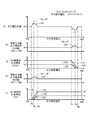
続いて、上記において説明した実施の形態1にかかる差動増幅器1の動作について出力設定電圧と出力誤差の定常特性とのグラフを示して、より具体的に説明する。図2、図3に差動増幅器1の出力設定電圧と出力誤差の定常特性のグラフを示す。
Subsequently, the operation of the
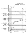
まず、入力電圧Vin1、Vin2が異なる場合について図2を参照して説明する。図2では、入力電圧Vin1が入力電圧Vin2より電圧差ΔV(>0)だけ高い電圧に設定される。図1の差動増幅器1の第1の差動対21と第2の差動対22は、内挿作用が正常に行われるときは、関連技術の出力アンプ188(図10)の上記式(7)及び(8)と同様の関係を満たしている。入力電圧Vin1が入力電圧Vin2より高電位のとき、電流I(31)、I(34)は、電流I(32)、I(33)より大きい。電流I(31)〜I(34)は、I(31)=I(34)=In2、I(32)=I(33)=In1、In2>In1という関係を有する。なお、合計電流(In2+In1)は電流源41、42のそれぞれの電流値(同一電流値)に対応している。また、第3の差動対23及び第4の差動対24も第1の差動対21及び第2の差動対22と同様の電流関係を有する。つまり、入力電圧Vin1がVin2より高電位で内挿作用が正常に行われるとき、電流I(37)、I(36)は、電流I(35)、I(38)より大きい。そして、電流I(35)〜I(38)は、I(37)=I(36)=Ip2、I(35)=I(38)=Ip1、Ip2>Ip1という関係を有する。合計電流(Ip2+Ip1)は電流源43、44のそれぞれの電流値(同一電流値)に対応している。なお、第3の差動対23及び第4の差動対24の各電流はドレイン・ソース間電流の絶対値で表す。なお、関連技術の出力アンプ188(図10)の特性(図12)との比較を容易にするため、図2の(2)、(4)及び(5)には、図12の(2)、(4)及び(5)の特性を一点鎖線で示す
First, the input voltage Vin1, Vin2 be described with reference to FIG vary. In FIG. 2, the input voltage Vin1 is set higher than the input voltage Vin2 by a voltage difference ΔV (> 0). The first
図2の(1)は、第1の差動対21及び第2の差動対22に流れる電流の特性を表している。電流I(31)、I(32)は実線、電流I(33)、I(34)は破線で示す。第1の差動対21及び第2の差動対22の各トランジスタに流れる電流は、出力設定電圧の範囲が高電位側電源電圧VDDに近い範囲では電流I(31)、I(34)はIn2、電流I(32)、I(33)はIn1で一定に保たれ、内挿作用は正常に行われる。一方、出力設定電圧の範囲が低電位側電源電圧VSSに近い範囲では、入力電圧Vin1、Vin2が低下して出力設定電圧が電圧Vdまで低下すると、低電位の入力電圧Vin2を受ける第2の差動対22の共通ソース端子が低電位側電源電圧VSSに達する。そして更に出力設定電圧が低下すると、第2の差動対22の共通ソース端子は低電位側電源電圧VSSより低下できないので、第2の差動対22のトランジスタ33、34のゲート・ソース間電圧が減少する。これにより電流I(33)、I(34)は出力設定電圧がVdより低下するに伴って減少を始める。ここで電圧Vdは第2の差動対22の動作電流が減少を開始する変化点となっている。そして、出力設定電圧が電圧Vbで電流I(33)、I(34)はほぼゼロとなり、Nch差動対(33、34)は停止する。第1の動作範囲は、出力設定電圧が電圧Vdから低電位側電源電圧VSSまでの範囲とされる。
(1) of FIG. 2 represents the characteristics of the current flowing through the first
一方、入力電圧Vin1を受ける第1の差動対21の共通ソース端子は抵抗R1を介して電流源41と接続されている。抵抗R1は、第1の動作範囲において、第2の差動対22の動作電流が減少を開始する変化点(Vd)に、第1の差動対21の動作電流が減少を開始する変化点を近づけるような抵抗値に設定されている。第1の差動対21の動作電流が減少を開始する変化点は、電流源41で設定される電流値と抵抗R1の抵抗値により定めることができる。図2では、第1の差動対21の動作電流が減少を開始する変化点を電圧Vdに設定した場合の例を示す。このような抵抗R1の設定において、入力電圧Vin1、Vin2が低下して出力設定電圧が電圧Vdまで低下すると、抵抗R1と電流源41との接続点電圧が低電位側電源電圧VSSに達する。そして、更に出力設定電圧が低下すると、抵抗R1と電流源41との接続点電圧が低電位側電源電圧VSSより低下できないので、抵抗R1に流れる電流が減少するとともに第1の差動対21のトランジスタ31、32のゲート・ソース間電圧も減少する。これにより電流I(31)、I(32)は出力設定電圧がVdより低下するに伴って減少を始める。そして出力設定電圧が電圧Vaで抵抗R1に流れる電流及び電流I(31)、I(32)はほぼゼロとなり、第1の差動対21は停止する。すなわち、第1の差動対21のトランジスタ対の電流減少開始電圧Vdは、抵抗R1によって、関連技術(図10)の電流減少開始電圧Vcよりも高電位側となり、電流の減少の度合いが緩やかになる。
On the other hand, the common source terminal of the first
図2の(2)は、差動入力部10の電流ノードN1、N2の出力電流差(I(N1)−I(N2))の特性(特性曲線Isn1)を表している。出力電流I(N1)は電流I(31)とI(33)の合計電流、出力電流I(N2)は電流I(32)とI(34)の合計電流である。出力電流I(N1)及び出力電流I(N2)は、出力増幅部11のカレントミラー60の出力側ノードに流れる電流と入力側ノードに流れる電流とそれぞれ合成される。出力電流差(I(N1)−I(N2))は、内挿作用が正常に行われる定常特性では通常ゼロとなる。図2の(2)では、出力電流差(I(N1)−I(N2))は、高電位側電源電圧VDD側ではゼロとなるが、低電位側電源電圧VSS近傍の出力設定電圧が電圧Vd〜Vaの範囲で正側に増加する。この出力電流差(I(N1)−I(N2))の増加は、図2の(1)の電流I(31)〜I(34)の変化に依存する。具体的には、図2の(1)において、出力設定電圧が電圧Vdより低下すると、電流I(33)、I(34)がそれぞれ減少する。このとき、電流I(33)の減少量より電流I(34)の減少量の方が大きい。また、電流I(31)、I(32)も出力設定電圧が電圧Vdより低下するとそれぞれ減少する。このとき、電流I(32)の減少量より電流I(31)の減少量の方が大きい。電流I(31)〜I(34)を演算した結果、出力電流差(I(N1)−I(N2))が正側に増加する。出力設定電圧がVbまで正側に増加して増加量がピークとなり、VbからVaで減少し、VaからVSSではゼロに戻る。
(2) in FIG. 2 represents the characteristic (characteristic curve Isn1) of the output current difference (I (N1) -I (N2)) between the current nodes N1 and N2 of the
図2の(2)より、差動増幅器1の出力電流差(I(N1)−I(N2))の増加(実線)は、抵抗R1が第1の動作範囲の第1の差動対21の動作電流の減少開始の変化点を移動させたことにより、関連技術(図12の(2))の出力電流差(I(N201)−I(N202))の増加(一点鎖線;特性曲線Isn_ref)よりも小さく抑えられている。
2 (2), the increase (solid line) in the output current difference (I (N1) -I (N2)) of the
なお、関連技術の図12の説明において、出力電流差(I(N201)−I(N202))が正側に増加したとき、それに対応して出力誤差も高電位側(正側)へ増加することを説明した。したがって、図2の(2)の出力電流差(I(N1)−I(N2))の特性(特性曲線Isn1)に対応する図2の(5)の出力誤差(特性曲線Ve1)は、高電位側(正側)へ増加するものの、関連技術(図12の(5))の出力誤差(一点鎖線;特性曲線Ve_ref)よりも小さく抑えられる。 In the description of FIG. 12 of the related art, when the output current difference (I (N201) −I (N202)) increases to the positive side, the output error correspondingly increases to the high potential side (positive side). I explained that. Therefore, the output error (characteristic curve Ve1) of FIG. 2 corresponding to the characteristic (characteristic curve Isn1) of the output current difference (I (N1) −I (N2)) of FIG. Although it increases to the potential side (positive side), it is suppressed to be smaller than the output error (dashed line; characteristic curve Ve_ref) of the related technique ((5) in FIG. 12).
図2の(3)は、第3の差動対23及び第4の差動対24に流れる電流の特性を表している。電流I(37)、I(38)は実線、電流I(35)、I(36)は破線で示す。第3の差動対23及び第4の差動対24の各トランジスタの電流は低電位側電源電圧VSS側ではI(35)、I(38)はIp1、I(36)、I(37)はIp2で一定に保たれ、内挿作用は正常に行われる。一方、高電位側電源電圧VDD近傍では、入力電圧Vin1、Vin2が上昇して出力設定電圧が電圧Veまで上昇すると、高電位の入力電圧Vin1を受ける第3の差動対23の共通ソース端子が高電位側電源電圧VDDに達する。そして更に出力設定電圧が上昇すると、第3の差動対23の共通ソース端子は高電位側電源電圧VDDより上昇できないので、第3の差動対23のトランジスタ35、36のゲート・ソース間電圧(絶対値)が減少する。これにより電流I(35)、I(36)は出力設定電圧がVeより上昇するに伴って減少を始める。そして、出力設定電圧が電圧Vgで電流I(35)、I(36)はほぼゼロとなり、第3の差動対23は停止する。第2の動作範囲は、出力設定電圧が電圧Veから高電位側電源電圧VDDまでの範囲とされる。また電圧Veは第3の差動対23の動作電流が減少を開始する変化点となっている。
(3) of FIG. 2 represents the characteristics of the current flowing through the third
一方、入力電圧Vin2を受ける第4の差動対24の共通ソース端子は抵抗R2を介して電流源44と接続されている。抵抗R2は、第2の動作範囲において、第3の差動対23の動作電流が減少を開始する変化点(Ve)に、第4の差動対24の動作電流が減少を開始する変化点を近づけるような抵抗値に設定されている。第4の差動対24の動作電流が減少を開始する変化点は、電流源44で設定される電流値と抵抗R2の抵抗値により定めることができる。図2では、第4の差動対24の動作電流が減少を開始する変化点を電圧Veに設定した場合の例を示す。このような抵抗R2の設定において、入力電圧Vin1、Vin2が上昇して出力設定電圧が電圧Veまで上昇すると、抵抗R2と電流源44との接続点電圧が高電位側電源電圧VDDに達する。そして更に出力設定電圧が上昇すると、抵抗R2と電流源44との接続点電圧が高電位側電源電圧VDDより上昇できないので、抵抗R2に流れる電流が減少するとともに第4の差動対24のトランジスタ37、38のゲート・ソース間電圧(絶対値)も減少する。これにより電流I(37)、I(38)は出力設定電圧がVeより上昇するに伴って減少を始める。そして、出力設定電圧が電圧Vhで抵抗R2に流れる電流及び電流I(37)、I(38)はほぼゼロとなり、第4の差動対24はオフする。すなわち、第4の差動対24のトランジスタ対の電流減少の開始電圧Veは、抵抗R2によって、関連技術(図12の(3))の電流減少開始電圧Vfよりも低電位側となり、電流の減少の度合いが緩やかになる。
On the other hand, the common source terminal of the fourth
図2の(4)は、差動入力部10の電流ノードN3、N4の出力電流差(I(N3)−I(N4))の特性(特性曲線Isp1)を表している。出力電流I(N3)は電流I(35)と電流I(37)の合計電流、出力電流I(N4)は電流I(36)とI(38)の合計電流で、それぞれ出力増幅部11のカレントミラー80の出力側ノードと入力側ノードの電流に結合されている。出力電流差(I(N3)−I(N4))は、内挿作用が正常に行われる定常特性では通常ゼロとなる。図2の(4)では、出力電流差(I(N3)−I(N4))は、低電位側電源電圧VSS側ではゼロとなるが、高電位側電源電圧VDD近傍で、出力設定電圧が電圧Ve〜Vhで正側に増加する。この出力電流差(I(N3)−I(N4))の増加は、図2の(3)の第3の差動対23及び第4の差動対24に流れる電流の変化に依存する。具体的には、図2の(3)において、出力設定電圧が電圧Veより上昇すると、電流I(35)、I(36)がそれぞれ減少する。このとき、電流I(35)の減少量よりも電流I(36)の減少量の方が大きい。また電流I(37)、I(38)も出力設定電圧が電圧Veより上昇するとそれぞれ減少する。電流I(35)〜I(38)の演算の結果、出力電流差(I(N3)−I(N4))が正側に増加する。出力設定電圧がVgまで正側に増加して増加量がピークとなり、VgからVhで減少し、Vhから高電位側電源電圧VDDまでの電圧範囲ではゼロに戻る。
(4) in FIG. 2 represents the characteristic (characteristic curve Isp1) of the output current difference (I (N3) -I (N4)) between the current nodes N3 and N4 of the
図2の(4)より、図1の差動増幅器1の出力電流差(I(N3)−I(N4))の増加(実線)は、抵抗R2が第2の動作範囲の第4の差動対24の動作電流の減少開始の変化点を移動させたことにより、関連技術(図12の(4))の出力電流差(I(N203)−I(N204))の増加(一点鎖線;特性曲線Isp_ref)よりも小さく抑えられている。
From (4) of FIG. 2, the increase (solid line) in the output current difference (I (N3) −I (N4)) of the
なお、関連技術の図12の説明において、出力電流差(I(N203)−I(N204))が正側に増加したとき、それに対応して出力誤差も低電位側(負側)へ増加することを説明した。したがって、図2の(4)の出力電流差(I(N3)−I(N4))の特性(特性曲線Isp1)に対応する図2の(5)の出力誤差(特性曲線Ve1)の絶対値は、低電位側(負側)へ増加するものの、関連技術(図12の(5))の出力誤差(一点鎖線;特性曲線Ve_ref)の絶対値よりも小さく抑えられる。 In the description of FIG. 12 of the related art, when the output current difference (I (N203) −I (N204)) increases to the positive side, the output error also increases correspondingly to the low potential side (negative side). I explained that. Accordingly, the absolute value of the output error (characteristic curve Ve1) of FIG. 2 corresponding to the characteristic (characteristic curve Isp1) of the output current difference (I (N3) −I (N4)) of FIG. Increases to the low potential side (negative side), but is suppressed to be smaller than the absolute value of the output error (dashed line; characteristic curve Ve_ref) of the related technique ((5) in FIG. 12).
以上、2つの入力電圧Vin1、Vin2が異なる場合において、抵抗R1、R2により図1の差動増幅器1の差動入力部10の出力電流差の増加が第1及び第2の動作範囲で抑えられ、それにより出力誤差の増加が関連技術の出力アンプ188(図10)より低減できることが示された。
As described above, when the two input voltages Vin1 and Vin2 are different from each other, an increase in the output current difference of the
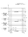
次に、図1の差動増幅器1の2つの入力電圧Vin1、Vin2が同一電圧(ΔV=0)の場合について図3を参照して説明する。入力電圧Vin1とVin2が同一電圧のとき、出力電圧Vout=Vin1(Vin2)となり、第1の差動対21の電流I(31)、I(32)及び第2の差動対22の電流I(33)、I(34)はそれぞれ同一電流となる。差動対21、22に電流源41、42で設定した動作電流が流れるときの、I(31)〜I(34)の電流を以下では電流In0と表す。また、第3の差動対23の電流I(35)、I(36)及び第4の差動対24のI(37)、I(38)はそれぞれ同一電流となる。差動対23、24に電流源43、44で設定した動作電流が流れるときの、I(35)〜I(38)の電流を以下では電流Ip0と表す。
Next, the case where the two input voltages Vin1 and Vin2 of the
図3の(1)は、第1の差動対21及び第2の差動対22に流れる電流の特性を表している。電流I(31)、I(32)は実線、電流I(33)、I(34)は破線で示す。第1の差動対21及び第2の差動対22に流れる電流I(31)〜I(34)は、高電位側電源電圧VDD側においてはIn0で一定に保たれる。一方、低電位側電源電圧VSS近傍では、入力電圧Vin1(Vin2)が低下して出力設定電圧(=Vin1)が電圧VDまで低下すると、第1の差動対21側の抵抗R1と電流源41との接続点電圧が低電位側電源電圧VSSに達する。そして更に出力設定電圧が低下すると、抵抗R1に流れる電流が減少するとともに第1の差動対21のトランジスタ31、32のゲート・ソース間電圧も減少する。これにより、電流I(31)、I(32)は出力設定電圧がVDより低下するに伴って減少を始める。そして出力設定電圧が電圧VAで抵抗R1に流れる電流及び電流I(31)、I(32)はほぼゼロとなり、第1の差動対21は停止する。入力電圧Vin1、Vin2が同一電圧の場合、出力設定電圧が電圧VDから低電位側電源電圧VSSまでの範囲が第1の動作範囲となる。
FIG. 3 (1) shows the characteristics of the current flowing through the first
一方、入力電圧Vin1(Vin2)が低下して出力設定電圧(=Vin1)が電圧VCまで低下すると、第2の差動対22の共通ソース端子が低電位側電源電圧VSSに達する。そして更に出力設定電圧が低下すると、第2の差動対22のトランジスタ33、34のゲート・ソース間電圧が減少する。これにより、電流I(33)、I(34)は出力設定電圧がVCより低下するに伴って減少を始める。そして出力設定電圧が電圧VAで電流I(33)、I(34)はほぼゼロとなり、第2の差動対22は停止する。すなわち、第1の差動対21のトランジスタ対の電流減少の開始電圧VDは、抵抗R1によって、第2の差動対22の電流減少の開始電圧VCよりも高電位側となり、電流の減少の度合いが緩やかになる。
On the other hand, when the input voltage Vin1 (Vin2) decreases and the output setting voltage (= Vin1) decreases to the voltage VC, the common source terminal of the second
図3の(2)は、差動入力部10の電流ノードN1、N2の出力電流差(I(N1)−I(N2))の特性を表している。出力電流差(I(N1)−I(N2))は、図3の(1)の第1の差動対21及び第2の差動対22に流れる電流の変化に依存する。図3の(1)では、電流I(31)、I(32)と電流I(33)、I(34)は、出力設定電圧が電圧VD〜VAで減少の仕方が異なるが、I(31)=I(32)及びI(33)=I(34)という関係を有するため、出力電流差(I(N1)−I(N2))は増加しない。したがって、図3の(2)の出力電流差(I(N1)−I(N2))の特性に対応する図3の(5)の出力誤差は、低電位側電源電圧VSS近傍でも増加しない。
(2) in FIG. 3 represents the characteristic of the output current difference (I (N1) -I (N2)) between the current nodes N1 and N2 of the
図3の(3)は、第3の差動対23及び第4の差動対24に流れる電流の特性を表している。電流I(37)、I(38)は実線、電流I(35)、I(36)は破線で示す。第3の差動対23及び第4の差動対24に流れる電流I(35)〜I(38)は、低電位側電源電圧VSS側においてIp0で一定に保たれる。一方、高電位側電源電圧VDD近傍では、入力電圧Vin1(Vin2)が上昇して出力設定電圧(=Vin1)が電圧VEまで上昇すると、第4の差動対24に接続される抵抗R2と電流源44との接続点電圧が高電位側電源電圧VDDに達する。そして更に出力設定電圧が上昇すると、抵抗R2に流れる電流が減少するとともに第4の差動対24のトランジスタ37、38のゲート・ソース間電圧も減少する。これにより電流I(37)、I(38)は出力設定電圧がVEより上昇するに伴って減少を始める。そして出力設定電圧が電圧VHで抵抗R2に流れる電流及び電流I(37)、I(38)はほぼゼロとなり、第4の差動対24は停止する。入力電圧Vin1、Vin2が同一電圧の場合、出力設定電圧が電圧VEから高電位側電源電圧VDDまでの範囲が第2の動作範囲となる。
FIG. 3 (3) shows the characteristics of the current flowing through the third
一方、入力電圧Vin1(Vin2)が上昇して出力設定電圧(=Vin1)が電圧VFまで上昇すると、第3の差動対23の共通ソース端子が高電位側電源電圧VDDに達する。そして更に出力設定電圧が上昇すると、第3の差動対23のトランジスタ35、36のゲート・ソース間電圧が減少する。これにより電流I(35)、I(36)は出力設定電圧がVFより上昇するに伴って減少を始める。そして出力設定電圧が電圧VHで電流I(35)、I(36)はほぼゼロとなり、第3の差動対23は停止する。すなわち、第4の差動対23のトランジスタ対の電流減少の開始電圧VEは、抵抗R2によって、第3の差動対24の電流減少の開始電圧VFよりも低電位側となり、電流の減少の度合いが緩やかになる。
On the other hand, when the input voltage Vin1 (Vin2) rises and the output setting voltage (= Vin1) rises to the voltage VF, the common source terminal of the third
図3の(4)は、差動入力部10の電流ノードN3、N4の出力電流差(I(N3)−I(N4))の特性を表している。出力電流差(I(N3)−I(N4))は、図3の(3)の第3の差動対23及び第4の差動対24に流れる電流の変化に依存する。図3の(3)では、電流I(35)、I(36)と電流I(37)、I(38)は、出力設定電圧が電圧VE〜VHで減少の仕方が異なるが、I(35)=I(36)及びI(37)=I(38)という関係を有するため、出力電流差(I(N3)−I(N4))は増加しない。したがって、図3の(4)の出力電流差(I(N3)−I(N4))の特性に対応する図3の(5)の出力誤差は、高電位側電源電圧VDD近傍でも増加しない。
(4) in FIG. 3 represents the characteristic of the output current difference (I (N3) -I (N4)) between the current nodes N3 and N4 of the
以上、2つの入力電圧Vin1、Vin2が同一の場合において、抵抗R1、R2による図1の差動増幅器1の差動入力部10の出力電流差の増加はなく、出力誤差の増加も生じないことが示された。
As described above, when the two input voltages Vin1 and Vin2 are the same, there is no increase in the output current difference of the
上記説明より、実施の形態1にかかる差動増幅器1では、第1の制御回路51及び第2の制御回路52により、差動入力部10の同一導電型の2組みの差動対により生成される2つの出力電流の差を低減する。これにより、差動増幅器1では、電源電圧近傍の出力誤差を低減することができる。また、差動増幅器1では、第1の制御回路51及び第2の制御回路52を抵抗R1、R2により構成する。つまり、差動増幅器1では、出力誤差を低減しながら、回路素子数の増大を抑制することができる。
From the above description, in the
実施の形態2
実施の形態2にかかる差動増幅器2の回路図を図4に示す。差動増幅器2は、差動増幅器1の第1の制御回路51及び第2の制御回路52の別の形態について示すものである。差動増幅器2では、第1の制御回路51の別の形態である第1の制御回路53と、第2の制御回路52の別の形態である第2の制御回路54と、を有する。なお、図4において、図1に示した差動増幅器1と同じ構成要素については、同一の符号を付して説明を省略する。また、図4では、図面を簡略化するために、出力増幅部11の詳細について省略した。また、差動増幅器2に入力される入力電圧Vin1、Vin2も、図1と同様に、入力電圧Vin1が入力電圧Vin2よりも高くなるか、又は、入力電圧Vin1、Vin2が同一電圧となるような電圧関係を有する場合で説明する。このため、第1の制御回路53は、電圧Vin1、Vin2のうち第1の電源電圧(低電位側電源電圧VSS)との電圧差が大きい電圧Vin1が入力される第1の差動対21と第1の電流源41との間に設けられ、第2の制御回路54は、電圧Vin1、Vin2のうち第2の電源電圧(高電位側電源電圧VDD)との電圧差が大きい電圧Vin2が入力される第4の差動対24と第4の電流源44との間に設けられる。
FIG. 4 shows a circuit diagram of the
第1の制御回路53は、第1の補助トランジスタTr1を有する。第1の補助トランジスタTr1は、第1導電型のトランジスタ(例えば、NMOSトランジスタ)である。そして、第1の補助トランジスタTr1は、第1端子(例えば、ソース)が第1の電流源41と第1の差動対21とを接続する第1の接続ノード(例えば、第1の差動対21の共通接続ノード)に接続され、制御端子(例えば、ゲート)に第1の制御電圧BNCが入力され、第2端子(例えば、ドレイン)に第1の電流供給端子(例えば、高電位側電源電圧VDDを供給する電源)が接続される。第1の補助トランジスタTr1の第1端子と第2端子間の電流(ドレイン・ソース間電流)は、第1の制御電圧BNCと第1の接続ノードの電圧との差に基づき制御される。第1の補助トランジスタTr1は、出力設定電圧が第1の動作範囲内で、入力電圧Vin1、Vin2の低下に応じて差動対21の動作電流が減少を始める変化点を制御する。具体的には、出力設定電圧が第1の動作範囲内で、第1の差動対21の共通ソース端子の下限電圧を第1の制御電圧BNCに基づき制御することにより、差動対21の動作電流が減少を始める変化点を制御する。
The
第1の制御電圧BNCは、入力電圧Vin1、Vin2が所定の電圧差ΔV(>0)を有するとき、入力電圧Vin1、Vin2が低下して、第2の差動対22に流れる電流(I(33)+I(34))が電流源42で設定された電流より減少し始める変化点に、第1の差動対21に流れる電流(I(31)+I(32))が電流源41で設定された電流より減少を始める変化点を近づけるような電圧値に設定される。第1の補助トランジスタTr1がNMOSトランジスタで構成されるとき、第1の差動対21の共通ソース端子の下限電圧は、第1の制御電圧BNCと第1の差動対21の共通ソース端子の電圧との差に基づくNMOSトランジスタTr1のドレイン・ソース電流が、電流源41により設定される電流値と同一となる電圧として定めることができる。第1の差動対21の共通ソース端子の下限電圧の制御に対応して、第1の差動対21の動作電流の変化点が制御される。なお、第1の差動対21と第2の差動対22に流れる電流が減少する変化点は必ずしも一致していなくても構わない。入力電圧Vin1、Vin2が所定の電圧差ΔVの取りうる値の範囲で、第1の差動対21と第2の差動対22に流れる電流が減少する変化点が十分近づくように制御されるのが好ましい。
The first control voltage BNC is such that when the input voltages Vin1 and Vin2 have a predetermined voltage difference ΔV (> 0), the input voltages Vin1 and Vin2 decrease and the current (I ( 33) + I (34)) starts to decrease from the current set by the
第2の制御回路54は、第2の補助トランジスタTr2を有する。第2の補助トランジスタTr2は、第2導電型のトランジスタ(例えば、PMOSトランジスタ)である。そして、第2の補助トランジスタTr2は、第1端子(例えば、ソース)が第4の電流源44と第4の差動対24とを接続する第2の接続ノード(例えば、第4の差動対24の共通接続ノード)に接続され、制御端子(例えば、ゲート)に第2の制御電圧BPCが入力され、第2端子(例えば、ドレイン)に第2の電流供給端子(例えば、低電位側電源電圧VSSを供給する電源)が接続される。第2の補助トランジスタTr2の第1端子と第2端子間の電流(ドレイン・ソース間電流)は、第2の制御電圧BPCと第2の接続ノードの電圧との差に基づき制御される。第2の補助トランジスタTr2は、出力設定電圧が第2の動作範囲内で、入力電圧Vin1、Vin2の上昇に応じて差動対24の動作電流が減少を始める変化点を制御する。具体的には、出力設定電圧が第2の動作範囲内で、第4の差動対24の共通接続ノードの上限電圧を第2の制御電圧BPCに基づき制御することにより、差動対24の動作電流が減少を始める変化点を制御する。
The
第2の制御電圧BPCは、入力電圧Vin1、Vin2が所定の電圧差ΔV(>0)を有するとき、入力電圧Vin1、Vin2が上昇して、第3の差動対23に流れる電流(I(35)+I(36))が電流源43で設定された電流より減少し始める変化点に、第4の差動対24に流れる電流(I(37)+I(38))が電流源44で設定された電流より減少を始める変化点を近づけるような電圧値に設定される。第2の補助トランジスタTr2がPMOSトランジスタで構成されるとき、第4の差動対24の共通ソース端子の上限電圧は、第2の制御電圧BPCと第4の差動対24の共通ソース端子の電圧との差に基づくPMOSトランジスタTr2のドレイン・ソース電流が、電流源44により設定される電流値と同一となる電圧として定めることができる。第4の差動対24の共通ソース端子の上限電圧の制御に対応して、第4の差動対24の動作電流の変化点が制御される。なお、第3の差動対23と第4の差動対24に流れる電流が減少する変化点は必ずしも一致していなくても構わない。入力電圧Vin1、Vin2が所定の電圧差ΔVの取りうる値の範囲で、第3の差動対23と第4の差動対24に流れる電流が減少する変化点が十分近づくように制御されるのが好ましい。
The second control voltage BPC is such that when the input voltages Vin1 and Vin2 have a predetermined voltage difference ΔV (> 0), the input voltages Vin1 and Vin2 rise and the current (I ( 35) + I (36)) starts to decrease from the current set by the
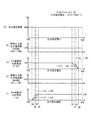
図4の差動増幅器2における第1の制御回路53及び第2の制御回路54による出力誤差抑制のメカニズムについて図5、図6を参照して説明する。図5、図6は、図4の差動増幅器2の作用を説明する図である。図1の差動増幅器1と同様に、図4の差動増幅器2においても、入力電圧Vin1、Vin2は、入力電圧Vin1が入力電圧Vin2よりも高くなるか、又は、Vin1とVin2が同一電圧となるような電圧関係を有し、どちらの場合でも電源電圧近傍の出力誤差の増加を抑制する作用を有する。
The mechanism of output error suppression by the
まず、入力電圧Vin1、Vin2が異なる場合について図5を参照して説明する。図5では、図4の差動増幅器2の入力電圧Vin1、Vin2は、Vin1がVin2より電圧差ΔV(>0)だけ高い電圧に設定されている。図4の差動増幅器2の第1の差動対21及び第2の差動対22は、内挿作用が正常に行われるときは、関連技術の出力アンプ188(10)の上記式(7)及び(8)と同様の関係を満たしている。入力電圧Vin1が入力電圧Vin2より高電位のとき、電流I(31)、I(34)は、電流I(32)、I(33)より大きい。そして、電流I(31)〜I(34)は、I(31)=I(34)=In2、I(32)=I(33)=In1、In2>In1という関係を有する。なお、合計電流(In2+In1)は電流源41、42のそれぞれの電流値(同一電流値)に対応している。また、第3の差動対23、第4の差動対24も同様に、入力電圧Vin1が入力電圧Vin2より高電位で内挿作用が正常に行われるとき、電流I(37)、I(36)は、電流I(35)及びI(38)より大きい。そして、電流I(35)〜I(38)は、I(37)=I(36)=Ip2、I(35)=I(38)=Ip1、Ip2>Ip1という関係を有する。合計電流(Ip2+Ip1)は電流源43、44のそれぞれの電流値(同一電流値)に対応している。なお、第3の差動対23及び第4の差動対24に流れる電流はドレイン・ソース間電流の絶対値で表す。なお、関連技術の出力アンプ188(図10)の特性(図12)との比較を容易にするため、図5の(2)、(4)及び(5)には、図12の(2)、(4)及び(5)の特性を一点鎖線で示す。
First, the case where the input voltages Vin1 and Vin2 are different will be described with reference to FIG. In FIG. 5, the input voltages Vin1 and Vin2 of the
図5の(1)は、第1の差動対21及び第2の差動対22に流れる電流の特性を表している。電流I(31)、I(32)は実線、電流I(33)、I(34)は破線で示す。出力設定電圧が高電位側電源電圧VDD側にある場合、第1の差動対21及び第2の差動対に流れる電流I(31)、I(34)はIn2で保たれ、第1の差動対21及び第2の差動対に流れる電流I(32)、I(33)はIn1に一定に保たれる。そして、第1の差動対21及び第2の差動対22の内挿作用は正常に行われる。一方、出力設定電圧が低電位側電源電圧VSS近傍にある場合、入力電圧Vin1、Vin2が低下して出力設定電圧が電圧Vdまで低下すると、低電位の入力電圧Vin2を受ける第2の差動対22の共通ソース端子が低電位側電源電圧VSSに達する。そして更に出力設定電圧が低下すると、第2の差動対22のトランジスタ33、34のゲート・ソース間電圧が減少する。これにより、電流I(33)、I(34)は出力設定電圧がVdより低下するに伴って減少を始める。そして、出力設定電圧が電圧Vbで電流I(33)、I(34)はほぼゼロとなり、第2の差動対22は停止する。第1の動作範囲は、出力設定電圧が電圧VdからVSSの範囲とされる。
(1) in FIG. 5 represents the characteristics of the current flowing through the first
一方、入力電圧Vin1を受ける第1の差動対21の共通ソース端子は第1の補助トランジスタTr1の制御電圧BNCにより下限電圧値が制御されている。制御電圧BNCは、第1の動作範囲において、第2の差動対22の動作電流が減少を開始する変化点(Vd)に、第1の差動対21の動作電流が減少を開始する変化点を近づけるような下限電圧値に設定される。図5では、第1の差動対21の動作電流が減少を開始する変化点が電圧Vd付近となるように設定した場合の例を示す。入力電圧Vin1、Vin2が低下して出力設定電圧が電圧Vdまで低下すると、第1の差動対21の共通ソース端子も第1の補助トランジスタTr1に制御される下限電圧値に達する。そして更に出力設定電圧が低下すると、第1の差動対21のトランジスタ31、32のゲート・ソース間電圧が減少する。これにより、電流I(31)、I(32)は出力設定電圧がVdより低下するに伴って減少を始める。そして、出力設定電圧が電圧Vbで電流I(31)、I(32)はほぼゼロとなり、第1の差動対21は停止する。すなわち、第1の差動対21のトランジスタ対の電流減少開始の変化点は、第1の補助トランジスタTr1によって、第2の差動対22のトランジスタ対の電流減少開始の変化点(Vd)にほぼ合わせることができる。
On the other hand, the lower limit voltage value of the common source terminal of the first
図5の(2)は、差動入力部10の電流ノードN1、N2の出力電流差(I(N1)−I(N2))の特性(特性曲線Isn2)を表している。出力電流I(N1)は第1の差動対21の電流I(31)と第2の差動対22の電流I(33)の合計電流、出力電流I(N2)は第1の差動対の電流I(32)と第2の差動対の電流I(34)の合計電流で、それぞれ出力増幅部11のカレントミラー60の出力ノードと入力ノードの電流に結合されている。出力電流差(I(N1)−I(N2))は、内挿作用が正常に行われる定常特性では通常ゼロとなる。図5の(2)において、図5の(1)の第1の差動対21及び第2の差動対22に流れる電流の変化に依存した出力電流差(I(N1)−I(N2))は、高電位側電源電圧VDD側ではゼロとなり、低電位側電源電圧VSS近傍では、出力設定電圧が電圧Vd〜Vbで若干の正側の増加があるものの十分小さい。
(2) in FIG. 5 represents the characteristic (characteristic curve Isn2) of the output current difference (I (N1) -I (N2)) between the current nodes N1 and N2 of the
図5の(2)より、出力電流差(I(N1)−I(N2))の増加(実線)は、第1の補助トランジスタTr1による第1の動作範囲の第1の差動対21の電流特性により、関連技術(図12の(2))の出力電流差(I(N1)−I(N2))の増加(一点鎖線;特性曲線Isn_ref)よりも大幅に小さく抑えられている。
From (2) in FIG. 5, the increase (solid line) in the output current difference (I (N1) −I (N2)) is caused by the first
なお、関連技術の図12の説明において、出力電流差(I(N1)−I(N2))が正側に増加したとき、それに対応して出力誤差も高電位側(正側)へ増加することを説明した。したがって、図5の(2)の出力電流差(I(N1)−I(N2))の特性(特性曲線Isn2)に対応する図5の(5)の出力誤差(特性曲線Ve2)は、高電位側(正側)へわずかな増加があるものの、関連技術(図12の(5))の出力誤差(一点鎖線;特性曲線Ve_ref)よりも大幅に小さく抑えられる。 In the description of FIG. 12 of the related art, when the output current difference (I (N1) −I (N2)) increases to the positive side, the output error correspondingly increases to the high potential side (positive side). I explained that. Therefore, the output error (characteristic curve Ve2) of FIG. 5 corresponding to the characteristic (characteristic curve Isn2) of the output current difference (I (N1) −I (N2)) of FIG. Although there is a slight increase toward the potential side (positive side), the output error (one-dot chain line; characteristic curve Ve_ref) of the related technique ((5) in FIG. 12) is suppressed to be significantly smaller.
図5の(3)は、第3の差動対23及び第4の差動対24に流れる電流の特性を表している。電流I(37)、I(38)は実線、電流I(35)、I(36)は破線で示す。出力設定電圧が低電位側電源電圧VSS側にある場合、第3の差動対23及び第4の差動対24に流れる電流I(35)、I(38)はIp1で保たれ、第3の差動対23及び第4の差動対24に流れる電流I(36)、I(37)はIp2に一定に保たれる。そして、第3の差動対23及び第4の差動対24の内挿作用は正常に行われる。一方、高電位側電源電圧VDD近傍では、入力電圧Vin1、Vin2が上昇して出力設定電圧が電圧Veまで上昇すると、高電位の入力電圧Vin1を受ける第3の差動対23の共通ソース端子が高電位側電源電圧VDDに達する。そして更に出力設定電圧が上昇すると、第3の差動対23のトランジスタ35、36のゲート・ソース間電圧(絶対値)が減少する。これにより、電流I(35)、I(36)は出力設定電圧がVeより上昇するに伴って減少を始める。そして、出力設定電圧が電圧Vgで電流I(35)、I(36)はほぼゼロとなり、第3の差動対(35、36)は停止する。第2の動作範囲は、出力設定電圧が電圧VeからVDDの範囲とされる。電圧Veは第3の差動対23の動作電流が減少を開始する変化点となっている。
(3) of FIG. 5 represents the characteristics of the current flowing through the third
一方、入力電圧Vin2を受ける第4の差動対24の共通ソース端子は第2の補助トランジスタTr2の制御電圧BPCにより上限電圧値が制御されている。制御電圧BPCは、第2の動作範囲において、第3の差動対23の動作電流が減少を開始する変化点(Ve)に、第4の差動対24の動作電流が減少を開始する変化点を近づけるような上限電圧値に設定される。図5では、第4の差動対24の動作電流が減少を開始する変化点が電圧Ve付近となるように設定した場合の例を示す。入力電圧Vin1、Vin2が上昇して出力設定電圧が電圧Veまで上昇すると、第4の差動対24の共通ソース端子も第2の補助トランジスタTr2に制御される上限電圧値に達する。そして更に出力設定電圧が上昇すると、第4の差動対24のトランジスタ37、38のゲート・ソース間電圧も減少する。これにより、電流I(37)、I(38)は出力設定電圧がVeより上昇するに伴って減少を始める。そして出力設定電圧が電圧Vgで電流I(37)、I(38)はほぼゼロとなり、第4の差動対24は停止する。すなわち、第4の差動対24のトランジスタ対の電流減少開始の変化点は、第2の補助トランジスタTr2によって、第3の差動対23のトランジスタ対の電流減少開始の変化点(Ve)にほぼ合わせることができる。
On the other hand, the upper limit voltage value of the common source terminal of the fourth
図5の(4)は、差動入力部10の電流ノードN3、N4の出力電流差(I(N3)−I(N4))の特性(特性曲線Isp2)を表している。出力電流I(N3)は第3の差動対23の電流I(35)と第4の差動対24の電流I(37)の合計電流、出力電流I(N4)は第3の差動対の電流I(36)と第4の差動対24の電流I(38)の合計電流で、それぞれ出力増幅部11のカレントミラー80の出力側ノードと入力側ノードの電流に結合されている。出力電流差(I(N3)−I(N4))は、内挿作用が正常に行われる定常特性では通常ゼロとなる。図5の(4)において、図5の(3)のPch差動対の各電流の変化に依存した出力電流差(I(N3)−I(N4))は、低電位側電源電圧VSS側ではゼロとなり、高電位側電源電圧VDD近傍では、出力設定電圧が電圧Ve〜Vgで若干の正側の増加があるものの十分小さい。
(4) in FIG. 5 represents the characteristic (characteristic curve Isp2) of the output current difference (I (N3) -I (N4)) between the current nodes N3 and N4 of the
図5の(4)より、出力電流差(I(N3)−I(N4))の増加(実線)は、第2の補助トランジスタTr2による第2の動作範囲の第4の差動対24の電流特性により、関連技術(図12の(4))の出力電流差(I(N3)−I(N4))の増加(一点鎖線;特性曲線Isp_ref)よりも大幅に小さく抑えられている。
From (4) of FIG. 5, the increase (solid line) in the output current difference (I (N3) −I (N4)) is that of the fourth
なお、関連技術の図12の説明において、出力電流差(I(N3)−I(N4))が正側に増加したとき、それに対応して出力誤差も低電位側(負側)へ増加することを説明した。したがって、図5の(4)の出力電流差(I(N3)−I(N4))の特性(特性曲線Isp2)に対応する図5の(5)の出力誤差(特性曲線Ve2)は、低電位側(負側)へ増加するものの、関連技術(図12の(5))の出力誤差(一点鎖線;特性曲線Ve_ref)よりも大幅に小さく抑えられる。 In the description of FIG. 12 of the related art, when the output current difference (I (N3) −I (N4)) increases to the positive side, the output error also increases correspondingly to the low potential side (negative side). I explained that. Accordingly, the output error (characteristic curve Ve2) of FIG. 5 corresponding to the characteristic (characteristic curve Isp2) of the output current difference (I (N3) −I (N4)) of FIG. Although it increases to the potential side (negative side), the output error (one-dot chain line; characteristic curve Ve_ref) of the related technique ((5) in FIG. 12) is suppressed to be significantly smaller.
以上、2つの入力電圧Vin1、Vin2が異なる場合において、第1の補助トランジスタTr1及び第2の補助トランジスタTr2により図4の差動増幅器2の差動入力部10の出力電流差の増加が第1及び第2の動作範囲で十分小さく抑えられ、それにより出力誤差の増加が関連技術(図10)の出力アンプ188より大幅に低減できることが示された。
As described above, when the two input voltages Vin1 and Vin2 are different, the first auxiliary transistor Tr1 and the second auxiliary transistor Tr2 increase the output current difference of the
次に、図4の差動増幅器2の入力電圧Vin1、Vin2が同一電圧(ΔV=0)の場合について図6を参照して説明する。入力電圧Vin1とVin2が同一電圧のとき、出力電圧Vout=Vin1(Vin2)となり、第1の差動対21の電流I(31)、I(32)及び第2の差動対22の電流I(33)、I(34)はそれぞれ同一電流となる。差動対21、22に電流源41、42で設定した動作電流が流れるときの、I(31)〜I(34)の電流を電流In0とする。また、第3の差動対23の電流I(35)、I(36)及び第4の差動対24のI(37)、I(38)はそれぞれ同一電流となる。差動対23、24に電流源43、44で設定した動作電流が流れるときの、I(35)〜I(38)の電流を電流Ip0とする。
Next, the case where the input voltages Vin1 and Vin2 of the
図6の(1)は、第1の差動対21及び第2の差動対22に流れる電流の特性を表している。電流I(31)、I(32)は実線、電流I(33)、I(34)は破線で示す。出力設定電圧が高電位側電源電圧VDD側にある場合、第1の差動対21及び第2の差動対22に流れる電流I(31)〜I(34)はIn0に一定に保たれる。一方、出力設定電圧が低電位側電源電圧VSS近傍にある場合、入力電圧Vin1(Vin2)が低下して出力設定電圧(=Vin1)が電圧VDまで低下すると、第1の差動対21の共通ソース端子が第1の補助トランジスタTr1に制御される下限電圧値に達する。そして更に出力設定電圧が低下すると、第1の差動対21のトランジスタ31、32のゲート・ソース間電圧が減少する。これにより、電流I(31)、I(32)は出力設定電圧がVDより低下するに伴って減少を始める。そして、出力設定電圧が電圧VBで電流I(31)、I(32)はほぼゼロとなり、第1の差動対21は停止する。入力電圧Vin1、Vin2が同一電圧の場合、出力設定電圧が電圧VDから低電位側電源電圧VSSまでの範囲が第1の動作範囲となる。
(1) in FIG. 6 represents the characteristics of the current flowing through the first
一方、入力電圧Vin1(Vin2)が低下して出力設定電圧(=Vin1)が電圧VCまで低下すると、第2の差動対22の共通ソース端子が低電位側電源電圧VSSに達する。そして更に出力設定電圧が低下すると、第2の差動対22のトランジスタ33、34のゲート・ソース間電圧が減少する。これにより、電流I(33)、I(34)は出力設定電圧がVCより低下するに伴って減少を始める。そして出力設定電圧が電圧VAで電流I(33)、I(34)はほぼゼロとなり、第2の差動対22は停止する。すなわち、第1の差動対21のトランジスタ対の電流減少の開始電圧VDは、第1の補助トランジスタTr1によって、第2の差動対22の電流減少の開始電圧VCよりも高電位側となり、第1の差動対21の停止電圧(VB)も第2の差動対22の停止電圧(VA)より高電位側となる。
On the other hand, when the input voltage Vin1 (Vin2) decreases and the output setting voltage (= Vin1) decreases to the voltage VC, the common source terminal of the second
図6の(2)は、差動入力部10の電流ノードN1、N2の出力電流差(I(N1)−I(N2))の特性を表している。出力電流差(I(N1)−I(N2))は、図6の(1)の第1の差動対21及び第2の差動対22に流れる電流の変化に依存する。図6の(1)では、電流I(31)、I(32)と電流I(33)、I(34)は、出力設定電圧が電圧VD〜VAで減少の仕方が異なるが、I(31)=I(32)及びI(33)=I(34)という関係を有するため、出力電流差(I(N1)−I(N2))は増加しない。したがって、図6の(2)の出力電流差(I(N1)−I(N2))の特性に対応する図6の(5)の出力誤差は、低電位側電源電圧VSS近傍でも増加しない。
(2) in FIG. 6 represents the characteristic of the output current difference (I (N1) -I (N2)) between the current nodes N1 and N2 of the
図6の(3)は、第3の差動対23及び第4の差動対24に流れる電流の特性を表している。電流I(37)、I(38)は実線、電流I(35)、I(36)は破線で示す。出力設定電圧が低電位側電源電圧VSS側にある場合、第3の差動対23及び第4の差動対24に流れる電流I(31)〜I(34)はIp0で一定に保たれる。一方、出力設定電圧が高電位側電源電圧VDD近傍にある場合、入力電圧Vin1(Vin2)が上昇して出力設定電圧(=Vin1)が電圧VEまで上昇すると、第4の差動対24の共通ソース端子が第2の補助トランジスタTr2に制御される上限電圧値に達する。そして更に出力設定電圧が上昇すると、第4の差動対24のトランジスタ37、38のゲート・ソース間電圧が減少する。これにより、電流I(37)、I(38)は出力設定電圧がVEより上昇するに伴って減少を始める。そして、出力設定電圧が電圧VGで電流I(37)、I(38)はほぼゼロとなり、第4の差動対24は停止する。入力電圧Vin1、Vin2が同一電圧の場合、出力設定電圧が電圧VEから高電位側電源電圧VDDまでの範囲が第2の動作範囲となる。
FIG. 6 (3) shows the characteristics of the current flowing through the third
一方、入力電圧Vin1(Vin2)が上昇して出力設定電圧(=Vin1)が電圧VFまで上昇すると、第3の差動対23の共通ソース端子が高電位側電源電圧VDDに達する。そして更に出力設定電圧が上昇すると、第3の差動対23のトランジスタ35、36のゲート・ソース間電圧が減少する。これにより電流I(35)、I(36)は出力設定電圧がVFより上昇するに伴って減少を始める。そして出力設定電圧が電圧VHで電流I(35)、I(36)はほぼゼロとなり、第3の差動対23は停止する。すなわち、第4の差動対24のトランジスタ対の電流減少の開始電圧VEは、第2の補助トランジスタTr2によって、第3の差動対23の電流減少の開始電圧VFよりも低電位側となり、第4の差動対24の停止電圧(VG)も第3の差動対23の停止電圧(VH)より低電位側となる。
On the other hand, when the input voltage Vin1 (Vin2) rises and the output setting voltage (= Vin1) rises to the voltage VF, the common source terminal of the third
図6の(4)は、差動入力部10の電流ノードN3、N4の出力電流差(I(N3)−I(N4))の特性を表している。出力電流差(I(N3)−I(N4))は、図6の(3)の第3の差動対23及び第4の差動対24に流れる電流の変化に依存する。図6の(3)では、電流I(35)、I(36)と電流I(37)、I(38)は、出力設定電圧が電圧VE〜VHで減少の仕方が異なるが、I(35)=I(36)及びI(37)=I(38)のため、出力電流差(I(N3)−I(N4))は増加しない。したがって、図6の(4)の出力電流差(I(N3)−I(N4))の特性に対応する図6の(5)の出力誤差は、高電位側電源電圧VDD近傍でも増加しない。
(4) in FIG. 6 represents the characteristics of the output current difference (I (N3) -I (N4)) between the current nodes N3 and N4 of the
以上、入力電圧Vin1、Vin2が同一の場合において、第1の補助トランジスタTr1及び第2の補助トランジスタTr2による図4の差動増幅器2の差動入力部10の出力電流差の増加はなく、出力誤差の増加も生じないことが示された。
As described above, when the input voltages Vin1 and Vin2 are the same, there is no increase in the output current difference of the
上記説明より、実施の形態2にかかる差動増幅器2では、実施の形態1とは異なる形態の第1の制御回路53及び第2の制御回路54によって、電源電圧近傍の出力誤差を低減する。この第1の制御回路53及び第2の制御回路54は、トランジスタ1つで構成できる。そのため、差動増幅器2においても、実施の形態1にかかる差動増幅器1と同様に回路規模の増大を抑制しながら出力誤差の低減を実現できる。
From the above description, in the
実施の形態3
実施の形態3にかかる差動増幅器3の回路図を図7に示す。図7に示すように差動増幅器3は、出力増幅部11の別の形態となる出力増幅部11aを有する。なお、図7に示す差動増幅器3では、実施の形態1と同じ構成要素については図1の差動増幅器1と同じ符号を付して説明を省略する。
FIG. 7 shows a circuit diagram of the
出力増幅部11aは、第1のカレントミラー60及び第2のカレントミラー80に代えて第1のカレントミラー60a及び第2のカレントミラー80aを有する。第1のカレントミラー60aは、第1のカレントミラー60からPMOSトランジスタ63、64を除いたものである。また、第2のカレントミラー80aは、第2のカレントミラー80からNMOSトランジスタ83、84を除いたものである。
The
より具体的には、第1のカレントミラー60aは、第2の電源(例えば、高電位側電源)に接続される第2導電型の第1のトランジスタ対を有し、第1のトランジスタ対に第1の電流ノード対(N1、N2)が接続され、第1の電流ノード対(N1、N2)から出力される差動電流出力を受ける。ここで、第1のトランジスタ対は、第1のミラートランジスタ(例えば、PMOSトランジスタ61)と第2のミラートランジスタ(例えば、PMOトランジスタ62)を有する。
More specifically, the first
PMOSトランジスタ61、62は、第1端子(例えば、ソース)が高電位側電源に共通に接続され、制御端子(例えば、ゲート)が共通接続される。第1の電流ノード対(N1、N2)の一方のノード(例えば、電流ノードN1)は、PMOSトランジスタ62の第2端子(例えば、ドレイン)に接続され、第1の電流ノード対(N1、N2)の他方のノード(例えば、電流ノードN2)は、PMOSトランジスタ61の第2端子(例えば、ドレイン)に接続される。PMOSトランジスタ61のドレインは、第1のカレントミラー60aの入力ノードとなっており、PMOSトランジスタ61のゲートと接続される。PMOSトランジスタ62のドレインは、第1のカレントミラー60aの出力ノードとなっている。
The
第2のカレントミラー80aは、第1の電源(例えば、低電位側電源)に接続される第1導電型の第2のトランジスタ対を有し、第2のトランジスタ対に第2の電流ノード対(N3、N4)が接続され、第2の電流ノード対(N3、N4)から出力される差動電流出力を受ける。ここで、第2のトランジスタ対は、第3のミラートランジスタ(例えば、NMOSトランジスタ81)と第4のミラートランジスタ(例えば、NMOトランジスタ82)を有する。
The second
NMOSトランジスタ81、82は、第1端子(例えば、ソース)が低電位側電源に共通に接続され、制御端子(例えば、ゲート)が共通接続される。第2の電流ノード対(N3、N4)の一方のノード(例えば、電流ノードN3)は、NMOSトランジスタ82の第2端子(例えば、ドレイン)に接続され、第2の電流ノード対(N3、N4)の他方のノード(例えば、電流ノードN4)は、PMOSトランジスタ81の第2端子(例えば、ドレイン)に接続される。NMOSトランジスタ81のドレインは、第2のカレントミラー80aの入力ノードとなっており、NMOSトランジスタ81のゲートと接続される。NMOSトランジスタ82のドレインは、第2のカレントミラー80aの出力ノードとなっている。
The
出力増幅部11aを上記のような構成としても、出力増幅部11と同様の動作を行うことが可能である。また、出力増幅部11aは、出力増幅部11よりも回路素子数が少ないため、出力増幅部11aを用いることで差動増幅器3の回路素子数を削減することができる。なお、差動増幅器3では、差動入力部10の構成が差動増幅器1と同じであるため、差動増幅器1と同様に出力誤差を抑制することが可能である。また、図7の差動増幅器3において、差動入力部10を、差動増幅器2(図4)の差動入力部10aに置き換えてもよい。
Even if the
実施の形態4
実施の形態4にかかる差動増幅器4の回路図を図8に示す。なお、図8に示す差動増幅器4において、図1に示す差動増幅器1と同じ構成要素については図1と同じ符号を付して説明を省略する。
FIG. 8 shows a circuit diagram of the
図8に示すように、差動増幅器4では、差動入力部10に代えて差動入力部10bを有する。差動入力部10bでは、第2の制御回路52が設けられる位置が実施の形態1にかかる差動入力部10とは異なる。
As shown in FIG. 8, the
図8の差動入力部10bの構成において、低電位側電源電圧VSS近傍の第1の動作範囲を含む差動入力部10bの動作範囲において、入力電圧Vin1、Vin2が異なるときにはVin1>Vin2とされる。一方、高電位側電源電圧VDD近傍の第2の動作範囲を含む差動入力部10bの動作範囲において、入力電圧Vin1、Vin2が異なるときには、Vin1<Vin2とされる。このため、差動入力部10bでは、第1の制御回路51は、電圧Vin1、Vin2のうち第1の電源電圧(低電位側電源電圧VSS)との電圧差が大きい電圧Vin1が入力される第1の差動対21と第1の電流源41との間に設けられるが、第2の制御回路52は、電圧Vin1、Vin2のうち第2の電源電圧(高電位側電源電圧VDD)との電圧差が大きい電圧Vin1が入力される第3の差動対23と第3の電流源43との間に設けられる。すなわち、差動入力部10bでは、第2の制御回路52が第3の差動対23と第3の電流源43との間に設けられる。
In the configuration of the
図8の第2の制御回路52の作用は、図1の制御回路52の作用の説明において、Vin1とVin2とを読み替え、第3の差動対23(トランジスタ35、36)と第4の差動対24(トランジスタ37、38)を読み替えたものに対応する。したがって図2(3)及び図3(3)においても、Pch差動対の電流I(35)、I(36)を電流I(37)、I(38)に読み替える。すなわち、電流I(35)、I(36)の特性が実線となり、電流I(37)、I(38)の特性が破線に入れ替わる。これにより、図2(4)における、電流ノードN3、N4の出力電流差(I(N3)−I(N4))の第2の動作範囲の正側への増加は、負側への増加となる。また、図2(5)における、第2の動作範囲の低電位側(負側)の出力誤差は、高電位側(正側)の出力誤差となる。なお、第1の動作範囲の各特性は変わらない。
The operation of the
特に液晶表示装置のデータドライバでは、電源電圧VDD、VSS間の中間電圧をVCOMとし、VCOM〜VDD間を正極とし、VCOM〜VSS間を負極とし、正極と負極のそれぞれで階調電圧を出力する構成とされている。このような場合には、正極階調電圧を出力する場合と負極階調電圧を出力する場合とで差動増幅器に入力する入力電圧Vin1、Vin2の大小関係を極性毎独立にできる。したがって、入力電圧Vin1、Vin2が異なるとき、正極階調電圧と負極階調電圧ともにVin1>Vin2とするときは、実施の形態1の差動増幅器1が適用され、一方、正極階調電圧ではVin1>Vin2、負極階調電圧ではVin1<Vin2とするときには実施の形態4の差動増幅器4が適用される。実施の形態1と4のいずれにおいても、第1、第2の制御回路51、52は、第1の動作範囲及び第2の動作範囲において、入力電圧Vin1、Vin2のうちそれぞれの動作範囲で最寄りとなる電源電圧との電圧差が大きい入力電圧を受ける差動対に供給される電流源からの動作電流の変化点を制御するように設けられている。なお、実施の形態4にかかる第1の制御回路51及び第2の制御回路52として実施の形態2にかかる第1の制御回路53及び第2の制御回路54を用いることも可能である。
In particular, in a data driver of a liquid crystal display device, an intermediate voltage between the power supply voltages VDD and VSS is VCOM, a voltage between VCOM and VDD is a positive electrode, a voltage between VCOM and VSS is a negative electrode, and a gradation voltage is output on each of the positive electrode and the negative electrode. It is configured. In such a case, the magnitude relationship between the input voltages Vin1 and Vin2 input to the differential amplifier can be made independent for each polarity depending on whether the positive gradation voltage or the negative gradation voltage is output. Therefore, when the input voltages Vin1 and Vin2 are different and the positive grayscale voltage and the negative grayscale voltage both satisfy Vin1> Vin2, the
以上、実施形態1〜4において、アクティブマトリクス型表示装置を駆動するデータドライバの出力回路に好適な差動増幅器について説明した。実施形態1〜4の各差動増幅器は、図9のデータドライバの出力アンプ188に置き換え可能で、差動増幅器の内挿出力における電源電圧近傍の電圧範囲での出力誤差の増加を抑え、高精度な電圧出力が可能となる。実施形態1〜4の各差動増幅器を適用したデータドライバは、アクティブマトリクス型表示装置(液晶表示装置や有機発光ダイオード表示装置等)に用いることできる。
In the first to fourth embodiments, the differential amplifier suitable for the output circuit of the data driver that drives the active matrix display device has been described. Each of the differential amplifiers of the first to fourth embodiments can be replaced with the
なお、本発明は上記実施の形態に限られたものではなく、趣旨を逸脱しない範囲で適宜変更することが可能である。例えば、第1の連絡回路70及び第2の連絡回路72の回路構成は、一例であり、適宜構成を変更することが可能である。
Note that the present invention is not limited to the above-described embodiment, and can be changed as appropriate without departing from the spirit of the present invention. For example, the circuit configurations of the
1〜4 差動増幅器
10、10a、10b 差動入力部
11、11a 出力増幅部
21〜24 差動対
31〜34 NMOSトランジスタ
35〜38 PMOSトランジスタ
41〜44 電流源
51〜54 制御回路
60、60a、80、80a カレントミラー
61〜64 PMOSトランジスタ
70、72 連絡回路
71 電流源
73 NMOSトランジスタ
74 PMOSトランジスタ
81〜84 NMOSトランジスタ
91、92 出力トランジスタ
C1、C2 コンデンサ
LSI データドライバ
N1〜N4 電流ノード
R1、R2 抵抗
Tr1、Tr2 補助トランジスタ
1-4
Claims (12)
前記第1の入力電圧及び前記第2の入力電圧の一方と前記出力電圧との差に基づき第1の電流ノード対に第1の差動電流を出力し、第1導電型トランジスタで形成される第1の差動対と、
前記第1の入力電圧及び前記第2の入力電圧の他方と前記出力電圧との差に基づき前記第1の電流ノード対に第2の差動電流を出力し、前記第1導電型トランジスタで形成される第2の差動対と、
前記第1の入力電圧及び前記第2の入力電圧の前記一方と前記出力電圧との差に基づき第2の電流ノード対に第3の差動電流を出力し、第2導電型トランジスタで形成される第3の差動対と、
前記第1の入力電圧及び前記第2の入力電圧の前記他方と前記出力電圧との差に基づき前記第2の電流ノード対に第4の差動電流を出力し、前記第2導電型トランジスタで形成される第4の差動対と、
第1の電源電圧を供給する第1の電源と前記第1の差動対との間に設けられ、前記第1の差動対に動作電流を供給する第1の電流源と、
前記第1の電源と前記第2の差動対との間に設けられ、前記第2の差動対に動作電流を供給する第2の電流源と、
第2の電源電圧を供給する第2の電源と前記第3の差動対との間に設けられ、前記第3の差動対に動作電流を供給する第3の電流源と、
前記第2の電源と前記第4の差動対との間に設けられ、前記第4の差動対に動作電流を供給する第4の電流源と、
前記第1、第2の入力電圧と前記出力電圧に基づき前記第1の差動対及び前記第2の差動対にそれぞれ流れる電流量が前記第1の電流源及び前記第2の電流源により設定される動作電流よりも小さくなる第1の動作範囲において、前記第1の差動対に供給される動作電流の変化点を制御する第1の制御回路と、
前記第1、第2の入力電圧と前記出力電圧に基づき前記第3の差動対及び前記第4の差動対にそれぞれ流れる電流量が前記第3の電流源及び前記第4の電流源により設定される動作電流よりも小さくなる第2の動作範囲において、前記第3の差動対又は前記第4の差動対に供給される動作電流の変化点を制御する第2の制御回路と、
前記第1の電流ノード対から出力される前記第1及び第2の差動電流を合成した差動電流出力と、前記第2の電流ノード対から出力される前記第3及び第4の差動電流を合成した差動電流出力と、に基づき前記出力電圧を生成する出力増幅部と、を有し、
前記第1の制御回路は、第1導電型であって、前記第1の電流源と前記第1の差動対とを接続する接続ノードに第1端子が接続され、制御端子に第1の制御電圧が入力され、第1の電流供給端子に第2端子が接続される第1の補助トランジスタを有し、
前記第2の制御回路は、第2導電型であって、前記第3の電流源と前記第4の差動対との接続ノード又は前記第4の電流源と前記第4の差動対との接続ノードに第1端子が接続され、制御端子に第2の制御電圧が入力され、第2の電流供給端子に第2端子が接続される第2の補助トランジスタを有し、
前記第1の補助トランジスタの第1端子と第2端子間の電流が、前記第1の制御電圧と前記第1の補助トランジスタの第1端子の電圧との差に基づき制御され、前記第2の補助トランジスタの第1端子と第2端子間の電流が、前記第2の制御電圧と前記第2の補助トランジスタの第1端子の電圧との差に基づき制御される差動増幅器。 A differential amplifier that outputs an output voltage having a signal level between a first input voltage and a second input voltage,
A first differential current is output to a first current node pair based on a difference between one of the first input voltage and the second input voltage and the output voltage, and is formed of a first conductivity type transistor. A first differential pair;
A second differential current is output to the first current node pair based on the difference between the other of the first input voltage and the second input voltage and the output voltage, and formed by the first conductivity type transistor. A second differential pair,
A third differential current is output to a second current node pair based on a difference between the one of the first input voltage and the second input voltage and the output voltage, and is formed of a second conductivity type transistor. A third differential pair,
Based on the difference between the other of the first input voltage and the second input voltage and the output voltage, a fourth differential current is output to the second current node pair, and the second conductivity type transistor A fourth differential pair formed;
A first current source provided between a first power supply for supplying a first power supply voltage and the first differential pair, and for supplying an operating current to the first differential pair;
A second current source provided between the first power supply and the second differential pair and supplying an operating current to the second differential pair;
A third current source provided between a second power supply for supplying a second power supply voltage and the third differential pair, and for supplying an operating current to the third differential pair;
A fourth current source provided between the second power source and the fourth differential pair and supplying an operating current to the fourth differential pair;
The amounts of current flowing through the first differential pair and the second differential pair based on the first and second input voltages and the output voltage are caused by the first current source and the second current source, respectively. A first control circuit that controls a change point of the operating current supplied to the first differential pair in a first operating range that is smaller than a set operating current;
The amount of current flowing through the third differential pair and the fourth differential pair based on the first and second input voltages and the output voltage is determined by the third current source and the fourth current source, respectively. A second control circuit for controlling a change point of the operating current supplied to the third differential pair or the fourth differential pair in a second operating range smaller than a set operating current;
A differential current output obtained by combining the first and second differential currents output from the first current node pair, and the third and fourth differentials output from the second current node pair An output amplifier that generates the output voltage based on a differential current output obtained by combining currents ;
The first control circuit is of a first conductivity type, and a first terminal is connected to a connection node connecting the first current source and the first differential pair, and a first terminal is connected to the control terminal. Having a first auxiliary transistor to which a control voltage is input and a second terminal is connected to the first current supply terminal;
The second control circuit is of a second conductivity type, and is a connection node between the third current source and the fourth differential pair, or the fourth current source and the fourth differential pair. A first terminal is connected to the connection node, a second control voltage is input to the control terminal, and a second auxiliary transistor is connected to the second current supply terminal.
The current between the first terminal and the second terminal of the first auxiliary transistor is controlled based on the difference between the first control voltage and the voltage of the first terminal of the first auxiliary transistor, and the second A differential amplifier in which a current between a first terminal and a second terminal of the auxiliary transistor is controlled based on a difference between the second control voltage and a voltage of the first terminal of the second auxiliary transistor .
前記第2の制御回路は、前記第1の入力電圧及び前記第2の入力電圧の変化に対する定常特性において、前記第1の入力電圧及び前記第2の入力電圧が所定の電圧差を有するときに、前記第2の動作範囲において、前記第3の差動対又は前記第4の差動対に流れる動作電流を制御することで前記第2の電流ノード対から出力される差動電流出力の電流差の変動を抑制する請求項1又は2に記載の差動増幅器。 The first control circuit is configured such that the first input voltage and the second input voltage have a predetermined voltage difference in steady characteristics with respect to changes in the first input voltage and the second input voltage. In the first operating range, by controlling the operating current flowing through the first differential pair, the fluctuation of the current difference of the differential current output output from the first current node pair is suppressed,
The second control circuit is configured such that the first input voltage and the second input voltage have a predetermined voltage difference in steady characteristics with respect to changes in the first input voltage and the second input voltage. In the second operating range, the current of the differential current output output from the second current node pair by controlling the operating current flowing in the third differential pair or the fourth differential pair The differential amplifier according to claim 1, wherein variation in difference is suppressed.
前記第3及び第4の差動対は、それぞれ、第1端子が共通接続され、制御端子が入力対とされる第2導電型のトランジスタ対により構成される請求項1乃至3のいずれか1項に記載の差動増幅器。 Each of the first and second differential pairs includes a first conductivity type transistor pair in which a first terminal is commonly connected and a control terminal is an input pair.
It said third and fourth differential pairs, respectively, the first terminal is commonly connected, either composed claims 1 to 3 by the second conductivity type transistor pair control terminal is the input-to-one The differential amplifier according to item.
前記第2の差動対は、共通接続された第1端子により前記第2の電流源が出力する電流を受け、入力対をなす制御端子にそれぞれ前記第2の入力電圧及び前記出力電圧が入力される第1導電型の第3及び第4の差動入力トランジスタで構成され、
前記第3の差動対は、共通接続された第1端子により前記第3の電流源が出力する電流を受け、入力対をなす制御端子にそれぞれ前記第1の入力電圧及び前記出力電圧が入力される第2導電型の第5及び第6の差動入力トランジスタで構成され、
前記第4の差動対は、共通接続された第1端子により前記第4の電流源が出力する電流を受け、入力対をなす制御端子にそれぞれ前記第2の入力電圧及び前記出力電圧が入力される第2導電型の第7及び第8の差動入力トランジスタで構成され、
前記第1及び第3の差動入力トランジスタの第2端子が前記第1の電流ノード対の第1のノードに共通接続され、
前記第2及び第4の差動入力トランジスタの第2端子が前記第1の電流ノード対の第2のノードに共通接続され、
前記第5及び第7の差動入力トランジスタの第2端子が前記第2の電流ノード対の第1のノードに共通接続され、
前記第6及び第8の差動入力トランジスタの第2端子が前記第2の電流ノード対の第2のノードに共通接続される請求項1乃至4のいずれか1項に記載の差動増幅器。 The first differential pair receives a current output from the first current source through a first terminal connected in common, and the first input voltage and the output voltage are respectively input to control terminals forming an input pair. The first and second differential input transistors of the first conductivity type,
The second differential pair receives a current output from the second current source through a first terminal connected in common, and the second input voltage and the output voltage are input to control terminals forming an input pair, respectively. The first and third differential input transistors of the first conductivity type,
The third differential pair receives a current output from the third current source through a first terminal connected in common, and the first input voltage and the output voltage are input to control terminals forming an input pair, respectively. The second and fifth conductivity type fifth and sixth differential input transistors,
The fourth differential pair receives a current output from the fourth current source by a first terminal connected in common, and the second input voltage and the output voltage are input to control terminals forming an input pair, respectively. The second conductive type seventh and eighth differential input transistors,
A second terminal of the first and third differential input transistors is commonly connected to a first node of the first current node pair;
A second terminal of the second and fourth differential input transistors is commonly connected to a second node of the first current node pair;
A second terminal of each of the fifth and seventh differential input transistors is commonly connected to a first node of the second current node pair;
The sixth and differential amplifier according to any one of claims 1 to 4 second terminal of the differential input transistors of the eighth are commonly connected to a second node of said second current node pair.
前記第2の差動対は、共通接続された第1端子により前記第2の電流源が出力する電流を受け、入力対をなす制御端子にそれぞれ前記第2の入力電圧及び前記出力電圧が入力される第1導電型の第3及び第4の差動入力トランジスタで構成され、
前記第3の差動対は、共通接続された第1端子により前記第3の電流源が出力する電流を受け、入力対をなす制御端子にそれぞれ前記第2の入力電圧及び前記出力電圧が入力される第2導電型の第5及び第6の差動入力トランジスタで構成され、
前記第4の差動対は、共通接続された第1端子により前記第4の電流源が出力する電流を受け、入力対をなす制御端子にそれぞれ前記第1の入力電圧及び前記出力電圧が入力される第2導電型の第7及び第8の差動入力トランジスタで構成され、
前記第1及び第3の差動入力トランジスタの第2端子が前記第1の電流ノード対の第1のノードに共通接続され、
前記第2及び第4の差動入力トランジスタの第2端子が前記第1の電流ノード対の第2のノードに共通接続され、
前記第5及び第7の差動入力トランジスタの第2端子が前記第2の電流ノード対の第1のノードに共通接続され、
前記第6及び第8の差動入力トランジスタの第2端子が前記第2の電流ノード対の第2のノードに共通接続される請求項1乃至4のいずれか1項に記載の差動増幅器。 The first differential pair receives a current output from the first current source through a first terminal connected in common, and the first input voltage and the output voltage are respectively input to control terminals forming an input pair. The first and second differential input transistors of the first conductivity type,
The second differential pair receives a current output from the second current source through a first terminal connected in common, and the second input voltage and the output voltage are input to control terminals forming an input pair, respectively. The first and third differential input transistors of the first conductivity type,
The third differential pair receives a current output from the third current source through a first terminal connected in common, and the second input voltage and the output voltage are respectively input to control terminals forming an input pair. The second and fifth conductivity type fifth and sixth differential input transistors,
The fourth differential pair receives a current output from the fourth current source by a first terminal connected in common, and the first input voltage and the output voltage are input to control terminals forming an input pair, respectively. The second conductive type seventh and eighth differential input transistors,
A second terminal of the first and third differential input transistors is commonly connected to a first node of the first current node pair;
A second terminal of the second and fourth differential input transistors is commonly connected to a second node of the first current node pair;
A second terminal of each of the fifth and seventh differential input transistors is commonly connected to a first node of the second current node pair;
The sixth and differential amplifier according to any one of claims 1 to 4 second terminal of the differential input transistors of the eighth are commonly connected to a second node of said second current node pair.
前記第2の電源に接続される第2導電型の第1のトランジスタ対を有し、前記第1の電流ノード対から出力される差動電流出力を受ける第1のカレントミラーと、
前記第1の電源に接続される第1導電型の第2のトランジスタ対を有し、前記第2の電流ノード対から出力される差動電流出力を受ける第2のカレントミラーと、
前記第1のカレントミラーの入力ノードと第2のカレントミラーの入力ノードとの間に接続された第1の連絡回路と、
前記第1のカレントミラーの出力ノードと第2のカレントミラーの出力ノードとの間に接続された第2の連絡回路と、
前記出力電圧が出力される出力端子と前記第2の電源との間に接続され、制御端子が前記第1のカレントミラーの出力ノードと前記第2の連絡回路の一端との接続点に接続された第2導電型の第1の出力トランジスタと、
前記出力端子と前記第1の電源との間に接続され、制御端子が前記第2の連絡回路の他端に接続された第1導電型の第2の出力トランジスタと、
を備える請求項1乃至6のいずれか1項に記載の差動増幅器。 The output amplifier is
A first current mirror having a first transistor pair of a second conductivity type connected to the second power supply and receiving a differential current output output from the first current node pair;
A second current mirror having a second transistor pair of the first conductivity type connected to the first power supply and receiving a differential current output output from the second current node pair;
A first communication circuit connected between an input node of the first current mirror and an input node of the second current mirror;
A second connecting circuit connected between an output node of the first current mirror and an output node of the second current mirror;
The output terminal from which the output voltage is output is connected between the second power supply, and the control terminal is connected to a connection point between the output node of the first current mirror and one end of the second connection circuit. A first output transistor of the second conductivity type;
A second output transistor of a first conductivity type connected between the output terminal and the first power supply, and having a control terminal connected to the other end of the second connection circuit;
The differential amplifier according to any one of claims 1 to 6 .
前記第1のトランジスタ対は、第1端子が前記第1の電源に共通に接続され、制御端子が互いに接続される第1、第2のミラートランジスタで構成され、
前記第3のトランジスタ対は、第1端子が前記第1のミラートランジスタの第2端子に接続される第3のミラートランジスタと、第1端子が前記第2のミラートランジスタの第2端子に接続され、制御端子が前記第3のミラートランジスタの制御端子と接続され、当該制御端子に第1のバイアス電圧が印加される第4のミラートランジスタとで構成され、
前記第3のミラートランジスタの第2端子は、前記第1のミラートランジスタの制御端子及び前記第2のミラートランジスタの制御端子に接続され、かつ、前記第1のカレントミラーの入力ノードとなり、
前記第4のミラートランジスタの第2端子は、前記第1のカレントミラーの出力ノードとなり、
前記第1の電流ノード対の第2のノードは前記第1のミラートランジスタの第2端子に接続され、前記第1の電流ノード対の第1のノードは前記第2のミラートランジスタの第2端子に接続され、
前記第2のカレントミラーは、さらに第1導電型の第4のトランジスタ対を有し、
前記第2のトランジスタ対は、第1端子が前記第2の電源に共通に接続され、制御端子が互いに接続される第5、第6のミラートランジスタで構成され、
前記第4のトランジスタ対は、第1端子が前記第5のミラートランジスタの第2端子に接続される第7のミラートランジスタと、第1端子が前記第6のミラートランジスタの第2端子に接続され、制御端子が前記第7のミラートランジスタの制御端子と接続され、当該制御端子に第2のバイアス電圧が印加される第8のミラートランジスタで構成され、
前記第7のミラートランジスタの第2端子は、前記第5のミラートランジスタの制御端子及び前記第6のミラートランジスタの制御端子に接続され、かつ、前記第2のカレントミラーの入力ノードとなり、
前記第8のミラートランジスタの第2端子は、前記第2のカレントミラーの出力ノードとなり、
前記第2の電流ノード対の第2のノードは前記第5のミラートランジスタの第2端子に接続され、前記第2の電流ノード対の第1のノードは前記第6のミラートランジスタの第2端子に接続される請求項7に記載の差動増幅器。 The first current mirror further includes a third transistor pair of the second conductivity type,
The first transistor pair includes first and second mirror transistors having a first terminal commonly connected to the first power supply and a control terminal connected to each other,
The third transistor pair has a first terminal connected to the second terminal of the first mirror transistor, and a first terminal connected to the second terminal of the second mirror transistor. The control terminal is connected to the control terminal of the third mirror transistor, and the control terminal is configured by a fourth mirror transistor to which the first bias voltage is applied.
A second terminal of the third mirror transistor is connected to a control terminal of the first mirror transistor and a control terminal of the second mirror transistor, and serves as an input node of the first current mirror;
The second terminal of the fourth mirror transistor becomes an output node of the first current mirror,
A second node of the first current node pair is connected to a second terminal of the first mirror transistor, and a first node of the first current node pair is a second terminal of the second mirror transistor. Connected to
The second current mirror further includes a fourth transistor pair of the first conductivity type,
The second transistor pair includes fifth and sixth mirror transistors having a first terminal commonly connected to the second power supply and a control terminal connected to each other.
The fourth transistor pair has a first mirror terminal connected to a second terminal of the fifth mirror transistor and a first terminal connected to a second terminal of the sixth mirror transistor. The control terminal is connected to the control terminal of the seventh mirror transistor, and the control terminal includes an eighth mirror transistor to which the second bias voltage is applied.
A second terminal of the seventh mirror transistor is connected to a control terminal of the fifth mirror transistor and a control terminal of the sixth mirror transistor, and serves as an input node of the second current mirror;
The second terminal of the eighth mirror transistor becomes an output node of the second current mirror,
A second node of the second current node pair is connected to a second terminal of the fifth mirror transistor, and a first node of the second current node pair is a second terminal of the sixth mirror transistor. The differential amplifier according to claim 7 , which is connected to the differential amplifier.
前記第1のミラートランジスタの第2端子は、前記第1のミラートランジスタの制御端子及び前記第2のミラートランジスタの制御端子に接続され、かつ、前記第1のカレントミラーの入力ノードとなり、
前記第2のミラートランジスタの第2端子は、前記第1のカレントミラーの出力ノードとなり、
前記第1の電流ノード対の第2のノードは前記第1のミラートランジスタの第2端子に接続され、前記第1の電流ノード対の第1のノードは前記第2のミラートランジスタの第2端子に接続され、
前記第2のトランジスタ対は、第1端子が前記第1の電源に共通に接続され、制御端子が互いに接続される第3、第4のミラートランジスタで構成され、
前記第3のミラートランジスタの第2端子は、前記第3のミラートランジスタの制御端子及び前記第4のミラートランジスタの制御端子に接続され、かつ、前記第2のカレントミラーの入力ノードとなり、
前記第4のミラートランジスタの第2端子は、前記第2のカレントミラーの出力ノードとなり、
前記第2の電流ノード対の第2のノードは前記第3のミラートランジスタの第2端子に接続され、前記第2の電流ノード対の第1のノードは前記第4のミラートランジスタの第2端子に接続される請求項7に記載の差動増幅器。 The first transistor pair includes first and second mirror transistors having a first terminal commonly connected to the second power supply and a control terminal connected to each other.
A second terminal of the first mirror transistor is connected to a control terminal of the first mirror transistor and a control terminal of the second mirror transistor, and serves as an input node of the first current mirror;
A second terminal of the second mirror transistor serves as an output node of the first current mirror;
A second node of the first current node pair is connected to a second terminal of the first mirror transistor, and a first node of the first current node pair is a second terminal of the second mirror transistor. Connected to
The second transistor pair is composed of third and fourth mirror transistors having a first terminal commonly connected to the first power supply and a control terminal connected to each other,
A second terminal of the third mirror transistor is connected to a control terminal of the third mirror transistor and a control terminal of the fourth mirror transistor, and serves as an input node of the second current mirror;
The second terminal of the fourth mirror transistor becomes an output node of the second current mirror,
A second node of the second current node pair is connected to a second terminal of the third mirror transistor, and a first node of the second current node pair is a second terminal of the fourth mirror transistor. The differential amplifier according to claim 7 , which is connected to the differential amplifier.
前記第2の連絡回路は、互いに並列に接続される第1導電型の第1のフローティングトランジスタと第2導電型の第2のフローティングトランジスタを有し、
前記第1のフローティングトランジスタの制御端子には第3のバイアス電圧が与えられ、
前記第2のフローティングトランジスタの制御端子には第4のバイアス電圧が与えられる請求項7乃至9のいずれか1項に記載の差動増幅器。 The first communication circuit has a current source;
The second connection circuit includes a first conductivity type first floating transistor and a second conductivity type second floating transistor connected in parallel to each other,
A third bias voltage is applied to the control terminal of the first floating transistor,
Wherein the control terminal of the second floating transistor differential amplifier according to any one of the fourth claims 7 to 9 bias voltage is applied.
前記第1の入力電圧及び前記第2の入力電圧の一方と前記出力電圧との差に基づき第1の電流ノード対に第1の差動電流を出力し、第1導電型トランジスタで形成される第1の差動対と、 A first differential current is output to a first current node pair based on a difference between one of the first input voltage and the second input voltage and the output voltage, and is formed of a first conductivity type transistor. A first differential pair;
前記第1の入力電圧及び前記第2の入力電圧の他方と前記出力電圧との差に基づき前記第1の電流ノード対に第2の差動電流を出力し、前記第1導電型トランジスタで形成される第2の差動対と、 A second differential current is output to the first current node pair based on the difference between the other of the first input voltage and the second input voltage and the output voltage, and formed by the first conductivity type transistor. A second differential pair,
前記第1の入力電圧及び前記第2の入力電圧の前記一方と前記出力電圧との差に基づき第2の電流ノード対に第3の差動電流を出力し、第2導電型トランジスタで形成される第3の差動対と、 A third differential current is output to a second current node pair based on a difference between the one of the first input voltage and the second input voltage and the output voltage, and is formed of a second conductivity type transistor. A third differential pair,
前記第1の入力電圧及び前記第2の入力電圧の前記他方と前記出力電圧との差に基づき前記第2の電流ノード対に第4の差動電流を出力し、前記第2導電型トランジスタで形成される第4の差動対と、 Based on the difference between the other of the first input voltage and the second input voltage and the output voltage, a fourth differential current is output to the second current node pair, and the second conductivity type transistor A fourth differential pair formed;
第1の電源電圧を供給する第1の電源と前記第1の差動対との間に設けられ、前記第1の差動対に動作電流を供給する第1の電流源と、 A first current source provided between a first power supply for supplying a first power supply voltage and the first differential pair, and for supplying an operating current to the first differential pair;
前記第1の電源と前記第2の差動対との間に設けられ、前記第2の差動対に動作電流を供給する第2の電流源と、 A second current source provided between the first power supply and the second differential pair and supplying an operating current to the second differential pair;
第2の電源電圧を供給する第2の電源と前記第3の差動対との間に設けられ、前記第3の差動対に動作電流を供給する第3の電流源と、 A third current source provided between a second power supply for supplying a second power supply voltage and the third differential pair, and for supplying an operating current to the third differential pair;
前記第2の電源と前記第4の差動対との間に設けられ、前記第4の差動対に動作電流を供給する第4の電流源と、 A fourth current source provided between the second power source and the fourth differential pair and supplying an operating current to the fourth differential pair;
前記第1、第2の入力電圧と前記出力電圧に基づき前記第1の差動対及び前記第2の差動対にそれぞれ流れる電流量が前記第1の電流源及び前記第2の電流源により設定される動作電流よりも小さくなる第1の動作範囲において、前記第1の差動対に供給される動作電流の変化点を制御する第1の制御回路と、 The amounts of current flowing through the first differential pair and the second differential pair based on the first and second input voltages and the output voltage are caused by the first current source and the second current source, respectively. A first control circuit that controls a change point of the operating current supplied to the first differential pair in a first operating range that is smaller than a set operating current;
前記第1、第2の入力電圧と前記出力電圧に基づき前記第3の差動対及び前記第4の差動対にそれぞれ流れる電流量が前記第3の電流源及び前記第4の電流源により設定される動作電流よりも小さくなる第2の動作範囲において、前記第3の差動対又は前記第4の差動対に供給される動作電流の変化点を制御する第2の制御回路と、 The amount of current flowing through the third differential pair and the fourth differential pair based on the first and second input voltages and the output voltage is determined by the third current source and the fourth current source, respectively. A second control circuit for controlling a change point of the operating current supplied to the third differential pair or the fourth differential pair in a second operating range smaller than a set operating current;
前記第1の電流ノード対から出力される前記第1及び第2の差動電流を合成した差動電流出力と、前記第2の電流ノード対から出力される前記第3及び第4の差動電流を合成した差動電流出力と、に基づき前記出力電圧を生成する出力増幅部と、を有し、 A differential current output obtained by combining the first and second differential currents output from the first current node pair, and the third and fourth differentials output from the second current node pair An output amplifier that generates the output voltage based on a differential current output obtained by combining currents;
前記第1の制御回路は、前記第1の電流源と前記第1の差動対との間に接続された第1の抵抗素子を有し、 The first control circuit includes a first resistance element connected between the first current source and the first differential pair;
前記第2の制御回路は、前記第3の電流源と前記第3の差動対との間、又は、前記第4の電流源と前記第4の差動対との間、に接続される第2の抵抗素子を有する差動増幅器。 The second control circuit is connected between the third current source and the third differential pair or between the fourth current source and the fourth differential pair. A differential amplifier having a second resistance element.
Priority Applications (2)
| Application Number | Priority Date | Filing Date | Title |
|---|---|---|---|
| JP2010265075A JP5623883B2 (en) | 2010-11-29 | 2010-11-29 | Differential amplifier and data driver |
| US13/297,639 US8471633B2 (en) | 2010-11-29 | 2011-11-16 | Differential amplifier and data driver |
Applications Claiming Priority (1)
| Application Number | Priority Date | Filing Date | Title |
|---|---|---|---|
| JP2010265075A JP5623883B2 (en) | 2010-11-29 | 2010-11-29 | Differential amplifier and data driver |
Publications (3)
| Publication Number | Publication Date |
|---|---|
| JP2012119745A JP2012119745A (en) | 2012-06-21 |
| JP2012119745A5 JP2012119745A5 (en) | 2013-12-05 |
| JP5623883B2 true JP5623883B2 (en) | 2014-11-12 |
Family
ID=46126214
Family Applications (1)
| Application Number | Title | Priority Date | Filing Date |
|---|---|---|---|
| JP2010265075A Expired - Fee Related JP5623883B2 (en) | 2010-11-29 | 2010-11-29 | Differential amplifier and data driver |
Country Status (2)
| Country | Link |
|---|---|
| US (1) | US8471633B2 (en) |
| JP (1) | JP5623883B2 (en) |
Families Citing this family (51)
| Publication number | Priority date | Publication date | Assignee | Title |
|---|---|---|---|---|
| US9288082B1 (en) * | 2010-05-20 | 2016-03-15 | Kandou Labs, S.A. | Circuits for efficient detection of vector signaling codes for chip-to-chip communication using sums of differences |
| US9077386B1 (en) | 2010-05-20 | 2015-07-07 | Kandou Labs, S.A. | Methods and systems for selection of unions of vector signaling codes for power and pin efficient chip-to-chip communication |
| US9251873B1 (en) | 2010-05-20 | 2016-02-02 | Kandou Labs, S.A. | Methods and systems for pin-efficient memory controller interface using vector signaling codes for chip-to-chip communications |
| WO2014172377A1 (en) | 2013-04-16 | 2014-10-23 | Kandou Labs, S.A. | Methods and systems for high bandwidth communications interface |
| EP2997704B1 (en) | 2013-06-25 | 2020-12-16 | Kandou Labs S.A. | Vector signaling with reduced receiver complexity |
| US9806761B1 (en) | 2014-01-31 | 2017-10-31 | Kandou Labs, S.A. | Methods and systems for reduction of nearest-neighbor crosstalk |
| JP6317474B2 (en) | 2014-02-02 | 2018-04-25 | カンドウ ラボズ ソシエテ アノニム | Method and apparatus for low power chip-to-chip communication using constrained ISI ratio |
| EP3111607B1 (en) | 2014-02-28 | 2020-04-08 | Kandou Labs SA | Clock-embedded vector signaling codes |
| US9509437B2 (en) | 2014-05-13 | 2016-11-29 | Kandou Labs, S.A. | Vector signaling code with improved noise margin |
| US9112550B1 (en) | 2014-06-25 | 2015-08-18 | Kandou Labs, SA | Multilevel driver for high speed chip-to-chip communications |
| EP3138253A4 (en) | 2014-07-10 | 2018-01-10 | Kandou Labs S.A. | Vector signaling codes with increased signal to noise characteristics |
| CN106664272B (en) | 2014-07-21 | 2020-03-27 | 康杜实验室公司 | Method and apparatus for receiving data from a multi-point communication channel |
| WO2016019384A1 (en) | 2014-08-01 | 2016-02-04 | Kandou Labs, S.A. | Orthogonal differential vector signaling codes with embedded clock |
| US9674014B2 (en) | 2014-10-22 | 2017-06-06 | Kandou Labs, S.A. | Method and apparatus for high speed chip-to-chip communications |
| US9531352B1 (en) | 2015-06-24 | 2016-12-27 | Intel Corporation | Latched comparator circuit |
| KR102372931B1 (en) | 2015-06-26 | 2022-03-11 | 칸도우 랩스 에스에이 | High speed communications system |
| US10055372B2 (en) | 2015-11-25 | 2018-08-21 | Kandou Labs, S.A. | Orthogonal differential vector signaling codes with embedded clock |
| WO2017132292A1 (en) | 2016-01-25 | 2017-08-03 | Kandou Labs, S.A. | Voltage sampler driver with enhanced high-frequency gain |
| WO2017185070A1 (en) | 2016-04-22 | 2017-10-26 | Kandou Labs, S.A. | Calibration apparatus and method for sampler with adjustable high frequency gain |
| US10003454B2 (en) | 2016-04-22 | 2018-06-19 | Kandou Labs, S.A. | Sampler with low input kickback |
| US10333741B2 (en) | 2016-04-28 | 2019-06-25 | Kandou Labs, S.A. | Vector signaling codes for densely-routed wire groups |
| US10056903B2 (en) | 2016-04-28 | 2018-08-21 | Kandou Labs, S.A. | Low power multilevel driver |
| US10153591B2 (en) | 2016-04-28 | 2018-12-11 | Kandou Labs, S.A. | Skew-resistant multi-wire channel |
| US10193716B2 (en) | 2016-04-28 | 2019-01-29 | Kandou Labs, S.A. | Clock data recovery with decision feedback equalization |
| US9906358B1 (en) | 2016-08-31 | 2018-02-27 | Kandou Labs, S.A. | Lock detector for phase lock loop |
| US10411922B2 (en) | 2016-09-16 | 2019-09-10 | Kandou Labs, S.A. | Data-driven phase detector element for phase locked loops |
| KR102649350B1 (en) | 2016-09-19 | 2024-03-20 | 삼성전자주식회사 | Interpolation amplifier and source driver comprising thereof |
| CN106341120B (en) * | 2016-09-23 | 2018-04-06 | 京东方科技集团股份有限公司 | Output buffer and its method of work, source electrode driver and display panel |
| US10200188B2 (en) | 2016-10-21 | 2019-02-05 | Kandou Labs, S.A. | Quadrature and duty cycle error correction in matrix phase lock loop |
| US10372665B2 (en) | 2016-10-24 | 2019-08-06 | Kandou Labs, S.A. | Multiphase data receiver with distributed DFE |
| US10200218B2 (en) | 2016-10-24 | 2019-02-05 | Kandou Labs, S.A. | Multi-stage sampler with increased gain |
| KR20180055294A (en) | 2016-11-16 | 2018-05-25 | 삼성전자주식회사 | FBAR Oscillator and Gas Sensing System using the FBAR Oscillator |
| JP6826314B2 (en) * | 2016-12-27 | 2021-02-03 | ヤマハ株式会社 | Floating power circuits and amplifiers |
| JP6899259B2 (en) * | 2017-05-17 | 2021-07-07 | ラピスセミコンダクタ株式会社 | Semiconductor devices and data drivers |
| US10116468B1 (en) | 2017-06-28 | 2018-10-30 | Kandou Labs, S.A. | Low power chip-to-chip bidirectional communications |
| US10686583B2 (en) | 2017-07-04 | 2020-06-16 | Kandou Labs, S.A. | Method for measuring and correcting multi-wire skew |
| US10203226B1 (en) | 2017-08-11 | 2019-02-12 | Kandou Labs, S.A. | Phase interpolation circuit |
| US10164591B1 (en) * | 2017-08-23 | 2018-12-25 | Qualcomm Incorporated | Differential amplifier with common-mode biasing technique |
| US10496583B2 (en) | 2017-09-07 | 2019-12-03 | Kandou Labs, S.A. | Low power multilevel driver for generating wire signals according to summations of a plurality of weighted analog signal components having wire-specific sub-channel weights |
| US10326623B1 (en) | 2017-12-08 | 2019-06-18 | Kandou Labs, S.A. | Methods and systems for providing multi-stage distributed decision feedback equalization |
| US10554380B2 (en) | 2018-01-26 | 2020-02-04 | Kandou Labs, S.A. | Dynamically weighted exclusive or gate having weighted output segments for phase detection and phase interpolation |
| WO2019241081A1 (en) | 2018-06-12 | 2019-12-19 | Kandou Labs, S.A. | Passive multi-input comparator for orthogonal codes on a multi-wire bus |
| US10931249B2 (en) | 2018-06-12 | 2021-02-23 | Kandou Labs, S.A. | Amplifier with adjustable high-frequency gain using varactor diodes |
| EP3850751A1 (en) | 2018-09-10 | 2021-07-21 | Kandou Labs, S.A. | Programmable continuous time linear equalizer having stabilized high-frequency peaking for controlling operating current of a slicer |
| US10608849B1 (en) | 2019-04-08 | 2020-03-31 | Kandou Labs, S.A. | Variable gain amplifier and sampler offset calibration without clock recovery |
| US10574487B1 (en) | 2019-04-08 | 2020-02-25 | Kandou Labs, S.A. | Sampler offset calibration during operation |
| US10680634B1 (en) | 2019-04-08 | 2020-06-09 | Kandou Labs, S.A. | Dynamic integration time adjustment of a clocked data sampler using a static analog calibration circuit |
| US10721106B1 (en) | 2019-04-08 | 2020-07-21 | Kandou Labs, S.A. | Adaptive continuous time linear equalization and channel bandwidth control |
| US11303484B1 (en) | 2021-04-02 | 2022-04-12 | Kandou Labs SA | Continuous time linear equalization and bandwidth adaptation using asynchronous sampling |
| US11374800B1 (en) | 2021-04-14 | 2022-06-28 | Kandou Labs SA | Continuous time linear equalization and bandwidth adaptation using peak detector |
| US11456708B1 (en) | 2021-04-30 | 2022-09-27 | Kandou Labs SA | Reference generation circuit for maintaining temperature-tracked linearity in amplifier with adjustable high-frequency gain |
Family Cites Families (9)
| Publication number | Priority date | Publication date | Assignee | Title |
|---|---|---|---|---|
| US5311145A (en) | 1993-03-25 | 1994-05-10 | North American Philips Corporation | Combination driver-summing circuit for rail-to-rail differential amplifier |
| JP3506219B2 (en) | 1998-12-16 | 2004-03-15 | シャープ株式会社 | DA converter and liquid crystal driving device using the same |
| JP3888350B2 (en) * | 2003-12-10 | 2007-02-28 | セイコーエプソン株式会社 | Operational amplifier and driving circuit using the same |
| JP4826073B2 (en) * | 2004-08-05 | 2011-11-30 | 日本電気株式会社 | Differential amplifier and data driver for display device using the same |
| TWI310926B (en) * | 2005-01-24 | 2009-06-11 | Himax Tech Inc | Source driver and source driving method |
| US7425867B2 (en) * | 2005-09-30 | 2008-09-16 | Agere Systems Inc. | Differential input/differential output converter circuit |
| JP2010041131A (en) * | 2008-07-31 | 2010-02-18 | Toshiba Corp | Operational amplifier |
| JP2011135158A (en) * | 2009-12-22 | 2011-07-07 | Toshiba Corp | Differential amplifier circuit, amplifier circuit, and liquid crystal display driver |
| JP5275278B2 (en) * | 2010-03-16 | 2013-08-28 | ルネサスエレクトロニクス株式会社 | Differential amplifier and source driver |
-
2010
- 2010-11-29 JP JP2010265075A patent/JP5623883B2/en not_active Expired - Fee Related
-
2011
- 2011-11-16 US US13/297,639 patent/US8471633B2/en not_active Expired - Fee Related
Also Published As
| Publication number | Publication date |
|---|---|
| JP2012119745A (en) | 2012-06-21 |
| US20120133438A1 (en) | 2012-05-31 |
| US8471633B2 (en) | 2013-06-25 |
Similar Documents
| Publication | Publication Date | Title |
|---|---|---|
| JP5623883B2 (en) | Differential amplifier and data driver | |
| US10777119B2 (en) | Semiconductor device | |
| US8988402B2 (en) | Output circuit, data driver, and display device | |
| US7907136B2 (en) | Voltage generation circuit | |
| US9147361B2 (en) | Output circuit, data driver and display device | |
| JP5143431B2 (en) | Output buffer with improved output deviation and source driver for flat panel display having the same | |
| JP4237219B2 (en) | Data receiving circuit, data driver and display device | |
| JP4614704B2 (en) | Differential amplifier, data driver and display device | |
| US8217925B2 (en) | Display panel driver and display device | |
| JP2012119745A5 (en) | ||
| US20060028274A1 (en) | Differential amplifier, and data driver of display device using the same | |
| US6897726B2 (en) | Differential circuit, amplifier circuit, and display device using the amplifier circuit | |
| JP2008111875A (en) | Operational amplifier and display device | |
| US7508259B2 (en) | Differential amplifier and data driver for display | |
| US20110007058A1 (en) | Differential class ab amplifier circuit, driver circuit and display device | |
| JP2006078556A (en) | Source driver, electro-optical device, electronic equipment, and driving method | |
| JP2005017653A (en) | Current source circuit and semiconductor device with current source circuit | |
| US7554389B2 (en) | Differential amplifier and digital-to-analog converter | |
| US7078941B2 (en) | Driving circuit for display device | |
| US20100085344A1 (en) | Operational amplifier circuit and display apparatus | |
| JP3888350B2 (en) | Operational amplifier and driving circuit using the same | |
| KR20220108489A (en) | Output buffer and source driver including the same | |
| JP2006222842A (en) | Current drive circuit | |
| JP2010039152A (en) | Drive unit for display | |
| JP4386116B2 (en) | Impedance conversion circuit, source driver, electro-optical device, and electronic apparatus |
Legal Events
| Date | Code | Title | Description |
|---|---|---|---|
| A521 | Request for written amendment filed |
Free format text: JAPANESE INTERMEDIATE CODE: A523 Effective date: 20131017 |
|
| A621 | Written request for application examination |
Free format text: JAPANESE INTERMEDIATE CODE: A621 Effective date: 20131017 |
|
| A977 | Report on retrieval |
Free format text: JAPANESE INTERMEDIATE CODE: A971007 Effective date: 20140314 |
|
| A131 | Notification of reasons for refusal |
Free format text: JAPANESE INTERMEDIATE CODE: A131 Effective date: 20140624 |
|
| A521 | Request for written amendment filed |
Free format text: JAPANESE INTERMEDIATE CODE: A523 Effective date: 20140820 |
|
| TRDD | Decision of grant or rejection written | ||
| A01 | Written decision to grant a patent or to grant a registration (utility model) |
Free format text: JAPANESE INTERMEDIATE CODE: A01 Effective date: 20140909 |
|
| A61 | First payment of annual fees (during grant procedure) |
Free format text: JAPANESE INTERMEDIATE CODE: A61 Effective date: 20140925 |
|
| R150 | Certificate of patent or registration of utility model |
Ref document number: 5623883 Country of ref document: JP Free format text: JAPANESE INTERMEDIATE CODE: R150 |
|
| S531 | Written request for registration of change of domicile |
Free format text: JAPANESE INTERMEDIATE CODE: R313531 |
|
| R350 | Written notification of registration of transfer |
Free format text: JAPANESE INTERMEDIATE CODE: R350 |
|
| LAPS | Cancellation because of no payment of annual fees |