JP5613620B2 - Wiring board and manufacturing method thereof - Google Patents
Wiring board and manufacturing method thereof Download PDFInfo
- Publication number
- JP5613620B2 JP5613620B2 JP2011119619A JP2011119619A JP5613620B2 JP 5613620 B2 JP5613620 B2 JP 5613620B2 JP 2011119619 A JP2011119619 A JP 2011119619A JP 2011119619 A JP2011119619 A JP 2011119619A JP 5613620 B2 JP5613620 B2 JP 5613620B2
- Authority
- JP
- Japan
- Prior art keywords
- conductive layer
- groove
- layer
- substrate body
- wiring board
- Prior art date
- Legal status (The legal status is an assumption and is not a legal conclusion. Google has not performed a legal analysis and makes no representation as to the accuracy of the status listed.)
- Active
Links
- 238000004519 manufacturing process Methods 0.000 title claims description 38
- 239000000758 substrate Substances 0.000 claims description 106
- 229910052751 metal Inorganic materials 0.000 claims description 39
- 239000002184 metal Substances 0.000 claims description 39
- 238000000034 method Methods 0.000 claims description 39
- 239000010949 copper Substances 0.000 claims description 33
- 229910052802 copper Inorganic materials 0.000 claims description 20
- 239000010703 silicon Substances 0.000 claims description 19
- 229910052710 silicon Inorganic materials 0.000 claims description 19
- RYGMFSIKBFXOCR-UHFFFAOYSA-N Copper Chemical compound [Cu] RYGMFSIKBFXOCR-UHFFFAOYSA-N 0.000 claims description 18
- 238000009713 electroplating Methods 0.000 claims description 16
- 238000005530 etching Methods 0.000 claims description 15
- 230000002093 peripheral effect Effects 0.000 claims description 8
- 239000010936 titanium Substances 0.000 claims description 8
- RTAQQCXQSZGOHL-UHFFFAOYSA-N Titanium Chemical compound [Ti] RTAQQCXQSZGOHL-UHFFFAOYSA-N 0.000 claims description 4
- 229910052719 titanium Inorganic materials 0.000 claims description 4
- 239000012670 alkaline solution Substances 0.000 claims description 2
- 239000010410 layer Substances 0.000 description 432
- 238000007747 plating Methods 0.000 description 22
- 230000007547 defect Effects 0.000 description 20
- XUIMIQQOPSSXEZ-UHFFFAOYSA-N Silicon Chemical compound [Si] XUIMIQQOPSSXEZ-UHFFFAOYSA-N 0.000 description 17
- 239000000463 material Substances 0.000 description 17
- 238000010586 diagram Methods 0.000 description 14
- 230000004048 modification Effects 0.000 description 14
- 238000012986 modification Methods 0.000 description 14
- KWYUFKZDYYNOTN-UHFFFAOYSA-M Potassium hydroxide Chemical compound [OH-].[K+] KWYUFKZDYYNOTN-UHFFFAOYSA-M 0.000 description 12
- 239000004065 semiconductor Substances 0.000 description 10
- 239000012790 adhesive layer Substances 0.000 description 9
- 229910052581 Si3N4 Inorganic materials 0.000 description 8
- 229910004298 SiO 2 Inorganic materials 0.000 description 8
- VYPSYNLAJGMNEJ-UHFFFAOYSA-N Silicium dioxide Chemical compound O=[Si]=O VYPSYNLAJGMNEJ-UHFFFAOYSA-N 0.000 description 8
- HQVNEWCFYHHQES-UHFFFAOYSA-N silicon nitride Chemical compound N12[Si]34N5[Si]62N3[Si]51N64 HQVNEWCFYHHQES-UHFFFAOYSA-N 0.000 description 8
- WGTYBPLFGIVFAS-UHFFFAOYSA-M tetramethylammonium hydroxide Chemical compound [OH-].C[N+](C)(C)C WGTYBPLFGIVFAS-UHFFFAOYSA-M 0.000 description 8
- 230000000052 comparative effect Effects 0.000 description 7
- 239000004642 Polyimide Substances 0.000 description 6
- 229920001721 polyimide Polymers 0.000 description 6
- 230000008646 thermal stress Effects 0.000 description 6
- 235000012239 silicon dioxide Nutrition 0.000 description 5
- 229910045601 alloy Inorganic materials 0.000 description 4
- 239000000956 alloy Substances 0.000 description 4
- 229920005989 resin Polymers 0.000 description 4
- 239000011347 resin Substances 0.000 description 4
- 239000000377 silicon dioxide Substances 0.000 description 4
- 229910000679 solder Inorganic materials 0.000 description 4
- 239000011800 void material Substances 0.000 description 4
- 239000007864 aqueous solution Substances 0.000 description 3
- 239000013078 crystal Substances 0.000 description 3
- 239000003822 epoxy resin Substances 0.000 description 3
- 239000011521 glass Substances 0.000 description 3
- 150000003949 imides Chemical class 0.000 description 3
- 238000005498 polishing Methods 0.000 description 3
- 229920000647 polyepoxide Polymers 0.000 description 3
- 239000011342 resin composition Substances 0.000 description 3
- 239000000126 substance Substances 0.000 description 3
- 229910052718 tin Inorganic materials 0.000 description 3
- 229910018503 SF6 Inorganic materials 0.000 description 2
- ROOXNKNUYICQNP-UHFFFAOYSA-N ammonium persulfate Chemical compound [NH4+].[NH4+].[O-]S(=O)(=O)OOS([O-])(=O)=O ROOXNKNUYICQNP-UHFFFAOYSA-N 0.000 description 2
- 238000004380 ashing Methods 0.000 description 2
- UMIVXZPTRXBADB-UHFFFAOYSA-N benzocyclobutene Chemical compound C1=CC=C2CCC2=C1 UMIVXZPTRXBADB-UHFFFAOYSA-N 0.000 description 2
- 230000015572 biosynthetic process Effects 0.000 description 2
- 239000005388 borosilicate glass Substances 0.000 description 2
- 238000005229 chemical vapour deposition Methods 0.000 description 2
- ORTQZVOHEJQUHG-UHFFFAOYSA-L copper(II) chloride Chemical compound Cl[Cu]Cl ORTQZVOHEJQUHG-UHFFFAOYSA-L 0.000 description 2
- 238000000708 deep reactive-ion etching Methods 0.000 description 2
- 230000000694 effects Effects 0.000 description 2
- 238000009413 insulation Methods 0.000 description 2
- 230000003647 oxidation Effects 0.000 description 2
- 238000007254 oxidation reaction Methods 0.000 description 2
- 238000001020 plasma etching Methods 0.000 description 2
- 229920002577 polybenzoxazole Polymers 0.000 description 2
- 229910052709 silver Inorganic materials 0.000 description 2
- 238000004544 sputter deposition Methods 0.000 description 2
- SFZCNBIFKDRMGX-UHFFFAOYSA-N sulfur hexafluoride Chemical compound FS(F)(F)(F)(F)F SFZCNBIFKDRMGX-UHFFFAOYSA-N 0.000 description 2
- 229960000909 sulfur hexafluoride Drugs 0.000 description 2
- 229910021578 Iron(III) chloride Inorganic materials 0.000 description 1
- 229910007637 SnAg Inorganic materials 0.000 description 1
- 229910001870 ammonium persulfate Inorganic materials 0.000 description 1
- KGBXLFKZBHKPEV-UHFFFAOYSA-N boric acid Chemical compound OB(O)O KGBXLFKZBHKPEV-UHFFFAOYSA-N 0.000 description 1
- 239000004327 boric acid Substances 0.000 description 1
- 239000000919 ceramic Substances 0.000 description 1
- 239000011248 coating agent Substances 0.000 description 1
- 238000000576 coating method Methods 0.000 description 1
- 229960003280 cupric chloride Drugs 0.000 description 1
- 238000000151 deposition Methods 0.000 description 1
- 238000005516 engineering process Methods 0.000 description 1
- 239000011888 foil Substances 0.000 description 1
- 239000011810 insulating material Substances 0.000 description 1
- RBTARNINKXHZNM-UHFFFAOYSA-K iron trichloride Chemical compound Cl[Fe](Cl)Cl RBTARNINKXHZNM-UHFFFAOYSA-K 0.000 description 1
- 239000007788 liquid Substances 0.000 description 1
- 229920002120 photoresistant polymer Polymers 0.000 description 1
- 230000002040 relaxant effect Effects 0.000 description 1
- RMAQACBXLXPBSY-UHFFFAOYSA-N silicic acid Chemical compound O[Si](O)(O)O RMAQACBXLXPBSY-UHFFFAOYSA-N 0.000 description 1
- 230000035882 stress Effects 0.000 description 1
- 238000006467 substitution reaction Methods 0.000 description 1
- 238000001039 wet etching Methods 0.000 description 1
Images


Classifications
-
- H—ELECTRICITY
- H05—ELECTRIC TECHNIQUES NOT OTHERWISE PROVIDED FOR
- H05K—PRINTED CIRCUITS; CASINGS OR CONSTRUCTIONAL DETAILS OF ELECTRIC APPARATUS; MANUFACTURE OF ASSEMBLAGES OF ELECTRICAL COMPONENTS
- H05K3/00—Apparatus or processes for manufacturing printed circuits
- H05K3/40—Forming printed elements for providing electric connections to or between printed circuits
- H05K3/42—Plated through-holes or plated via connections
- H05K3/425—Plated through-holes or plated via connections characterised by the sequence of steps for plating the through-holes or via connections in relation to the conductive pattern
-
- H—ELECTRICITY
- H01—ELECTRIC ELEMENTS
- H01L—SEMICONDUCTOR DEVICES NOT COVERED BY CLASS H10
- H01L21/00—Processes or apparatus adapted for the manufacture or treatment of semiconductor or solid state devices or of parts thereof
- H01L21/02—Manufacture or treatment of semiconductor devices or of parts thereof
- H01L21/04—Manufacture or treatment of semiconductor devices or of parts thereof the devices having potential barriers, e.g. a PN junction, depletion layer or carrier concentration layer
- H01L21/48—Manufacture or treatment of parts, e.g. containers, prior to assembly of the devices, using processes not provided for in a single one of the subgroups H01L21/06 - H01L21/326
- H01L21/4814—Conductive parts
- H01L21/4846—Leads on or in insulating or insulated substrates, e.g. metallisation
- H01L21/486—Via connections through the substrate with or without pins
-
- H—ELECTRICITY
- H01—ELECTRIC ELEMENTS
- H01L—SEMICONDUCTOR DEVICES NOT COVERED BY CLASS H10
- H01L23/00—Details of semiconductor or other solid state devices
- H01L23/12—Mountings, e.g. non-detachable insulating substrates
- H01L23/14—Mountings, e.g. non-detachable insulating substrates characterised by the material or its electrical properties
- H01L23/147—Semiconductor insulating substrates
-
- H—ELECTRICITY
- H01—ELECTRIC ELEMENTS
- H01L—SEMICONDUCTOR DEVICES NOT COVERED BY CLASS H10
- H01L23/00—Details of semiconductor or other solid state devices
- H01L23/48—Arrangements for conducting electric current to or from the solid state body in operation, e.g. leads, terminal arrangements ; Selection of materials therefor
- H01L23/488—Arrangements for conducting electric current to or from the solid state body in operation, e.g. leads, terminal arrangements ; Selection of materials therefor consisting of soldered or bonded constructions
- H01L23/498—Leads, i.e. metallisations or lead-frames on insulating substrates, e.g. chip carriers
- H01L23/49827—Via connections through the substrates, e.g. pins going through the substrate, coaxial cables
-
- H—ELECTRICITY
- H01—ELECTRIC ELEMENTS
- H01L—SEMICONDUCTOR DEVICES NOT COVERED BY CLASS H10
- H01L2924/00—Indexing scheme for arrangements or methods for connecting or disconnecting semiconductor or solid-state bodies as covered by H01L24/00
- H01L2924/0001—Technical content checked by a classifier
- H01L2924/0002—Not covered by any one of groups H01L24/00, H01L24/00 and H01L2224/00
-
- H—ELECTRICITY
- H05—ELECTRIC TECHNIQUES NOT OTHERWISE PROVIDED FOR
- H05K—PRINTED CIRCUITS; CASINGS OR CONSTRUCTIONAL DETAILS OF ELECTRIC APPARATUS; MANUFACTURE OF ASSEMBLAGES OF ELECTRICAL COMPONENTS
- H05K1/00—Printed circuits
- H05K1/02—Details
- H05K1/03—Use of materials for the substrate
- H05K1/0306—Inorganic insulating substrates, e.g. ceramic, glass
-
- H—ELECTRICITY
- H05—ELECTRIC TECHNIQUES NOT OTHERWISE PROVIDED FOR
- H05K—PRINTED CIRCUITS; CASINGS OR CONSTRUCTIONAL DETAILS OF ELECTRIC APPARATUS; MANUFACTURE OF ASSEMBLAGES OF ELECTRICAL COMPONENTS
- H05K2201/00—Indexing scheme relating to printed circuits covered by H05K1/00
- H05K2201/03—Conductive materials
- H05K2201/0332—Structure of the conductor
- H05K2201/0335—Layered conductors or foils
- H05K2201/0347—Overplating, e.g. for reinforcing conductors or bumps; Plating over filled vias
-
- H—ELECTRICITY
- H05—ELECTRIC TECHNIQUES NOT OTHERWISE PROVIDED FOR
- H05K—PRINTED CIRCUITS; CASINGS OR CONSTRUCTIONAL DETAILS OF ELECTRIC APPARATUS; MANUFACTURE OF ASSEMBLAGES OF ELECTRICAL COMPONENTS
- H05K2201/00—Indexing scheme relating to printed circuits covered by H05K1/00
- H05K2201/09—Shape and layout
- H05K2201/09209—Shape and layout details of conductors
- H05K2201/095—Conductive through-holes or vias
- H05K2201/09563—Metal filled via
-
- H—ELECTRICITY
- H05—ELECTRIC TECHNIQUES NOT OTHERWISE PROVIDED FOR
- H05K—PRINTED CIRCUITS; CASINGS OR CONSTRUCTIONAL DETAILS OF ELECTRIC APPARATUS; MANUFACTURE OF ASSEMBLAGES OF ELECTRICAL COMPONENTS
- H05K2201/00—Indexing scheme relating to printed circuits covered by H05K1/00
- H05K2201/09—Shape and layout
- H05K2201/09818—Shape or layout details not covered by a single group of H05K2201/09009 - H05K2201/09809
- H05K2201/09827—Tapered, e.g. tapered hole, via or groove
-
- H—ELECTRICITY
- H05—ELECTRIC TECHNIQUES NOT OTHERWISE PROVIDED FOR
- H05K—PRINTED CIRCUITS; CASINGS OR CONSTRUCTIONAL DETAILS OF ELECTRIC APPARATUS; MANUFACTURE OF ASSEMBLAGES OF ELECTRICAL COMPONENTS
- H05K2201/00—Indexing scheme relating to printed circuits covered by H05K1/00
- H05K2201/09—Shape and layout
- H05K2201/09818—Shape or layout details not covered by a single group of H05K2201/09009 - H05K2201/09809
- H05K2201/09845—Stepped hole, via, edge, bump or conductor
-
- H—ELECTRICITY
- H05—ELECTRIC TECHNIQUES NOT OTHERWISE PROVIDED FOR
- H05K—PRINTED CIRCUITS; CASINGS OR CONSTRUCTIONAL DETAILS OF ELECTRIC APPARATUS; MANUFACTURE OF ASSEMBLAGES OF ELECTRICAL COMPONENTS
- H05K2201/00—Indexing scheme relating to printed circuits covered by H05K1/00
- H05K2201/09—Shape and layout
- H05K2201/09818—Shape or layout details not covered by a single group of H05K2201/09009 - H05K2201/09809
- H05K2201/09854—Hole or via having special cross-section, e.g. elliptical
-
- H—ELECTRICITY
- H05—ELECTRIC TECHNIQUES NOT OTHERWISE PROVIDED FOR
- H05K—PRINTED CIRCUITS; CASINGS OR CONSTRUCTIONAL DETAILS OF ELECTRIC APPARATUS; MANUFACTURE OF ASSEMBLAGES OF ELECTRICAL COMPONENTS
- H05K2203/00—Indexing scheme relating to apparatus or processes for manufacturing printed circuits covered by H05K3/00
- H05K2203/01—Tools for processing; Objects used during processing
- H05K2203/0147—Carriers and holders
- H05K2203/0152—Temporary metallic carrier, e.g. for transferring material
-
- H—ELECTRICITY
- H05—ELECTRIC TECHNIQUES NOT OTHERWISE PROVIDED FOR
- H05K—PRINTED CIRCUITS; CASINGS OR CONSTRUCTIONAL DETAILS OF ELECTRIC APPARATUS; MANUFACTURE OF ASSEMBLAGES OF ELECTRICAL COMPONENTS
- H05K2203/00—Indexing scheme relating to apparatus or processes for manufacturing printed circuits covered by H05K3/00
- H05K2203/15—Position of the PCB during processing
- H05K2203/1572—Processing both sides of a PCB by the same process; Providing a similar arrangement of components on both sides; Making interlayer connections from two sides
-
- H—ELECTRICITY
- H05—ELECTRIC TECHNIQUES NOT OTHERWISE PROVIDED FOR
- H05K—PRINTED CIRCUITS; CASINGS OR CONSTRUCTIONAL DETAILS OF ELECTRIC APPARATUS; MANUFACTURE OF ASSEMBLAGES OF ELECTRICAL COMPONENTS
- H05K3/00—Apparatus or processes for manufacturing printed circuits
- H05K3/0011—Working of insulating substrates or insulating layers
- H05K3/0017—Etching of the substrate by chemical or physical means
- H05K3/002—Etching of the substrate by chemical or physical means by liquid chemical etching
-
- Y—GENERAL TAGGING OF NEW TECHNOLOGICAL DEVELOPMENTS; GENERAL TAGGING OF CROSS-SECTIONAL TECHNOLOGIES SPANNING OVER SEVERAL SECTIONS OF THE IPC; TECHNICAL SUBJECTS COVERED BY FORMER USPC CROSS-REFERENCE ART COLLECTIONS [XRACs] AND DIGESTS
- Y10—TECHNICAL SUBJECTS COVERED BY FORMER USPC
- Y10T—TECHNICAL SUBJECTS COVERED BY FORMER US CLASSIFICATION
- Y10T29/00—Metal working
- Y10T29/49—Method of mechanical manufacture
- Y10T29/49002—Electrical device making
- Y10T29/49117—Conductor or circuit manufacturing
- Y10T29/49124—On flat or curved insulated base, e.g., printed circuit, etc.
Landscapes
- Engineering & Computer Science (AREA)
- Microelectronics & Electronic Packaging (AREA)
- Physics & Mathematics (AREA)
- Condensed Matter Physics & Semiconductors (AREA)
- General Physics & Mathematics (AREA)
- Computer Hardware Design (AREA)
- Power Engineering (AREA)
- Manufacturing & Machinery (AREA)
- Ceramic Engineering (AREA)
- Printing Elements For Providing Electric Connections Between Printed Circuits (AREA)
- Internal Circuitry In Semiconductor Integrated Circuit Devices (AREA)
Description
本発明は、溝及び貫通孔を有する配線基板、及びその製造方法に関する。 The present invention relates to a wiring board having a groove and a through hole, and a manufacturing method thereof.
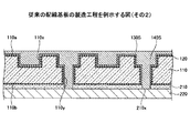
図1は、従来の配線基板を例示する断面図である。図1を参照するに、配線基板100は、基板本体110と、第1絶縁層120と、第1導電層130と、第2導電層140と、第2絶縁層150と、第3絶縁層160と、第1外部接続端子170と、第2外部接続端子180とを有する。
FIG. 1 is a cross-sectional view illustrating a conventional wiring board. Referring to FIG. 1, the
配線基板100において、基板本体110は、第1導電層130等を形成する基体となる部分であり、溝110xと、溝110xに連通する貫通孔110yとが形成されている。第1絶縁層120は、基板本体110の面110a及び110b、溝110xの内底面及び内側面、並びに貫通孔110yの内側面に形成されている。
In the
第1導電層130は、溝110xの内底面及び内側面、並びに貫通孔110yの内側面を被覆する第1絶縁層120上に形成されている。第2導電層140は、第1導電層130上に、溝110x及び貫通孔110yを充填するように形成されている。第1導電層130は、第2導電層140と電気的に接続されている。
The first
第2絶縁層150は、基板本体110の面110aを被覆する第1絶縁層120上、並びに第1導電層130及び第2導電層140の一部の上に形成されている。第2絶縁層150は開口部150xを有し、開口部150xの底部には第2導電層140の一部が露出している。
The second
第3絶縁層160は、基板本体110の面110bを被覆する第1絶縁層120上、並びに第1導電層130及び第2導電層140の一部の上に形成されている。第3絶縁層160は開口部160xを有し、開口部160xの底部には第2導電層140の一部が露出している。
The third
第1外部接続端子170は、開口部150xの底部に露出する第2導電層140上に形成されている。第1外部接続端子170は、第2導電層140と電気的に接続されている。第2外部接続端子180は、開口部160xの底部に露出する第2導電層140上に形成されている。第2外部接続端子180は、第2導電層140と電気的に接続されている。
The first
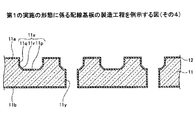
図2〜図4は、従来の配線基板の製造工程を例示する図である。始めに、図2に示す工程では、基板本体110に溝110xと、溝110xに連通する貫通孔110yとを形成し、基板本体110の面110a及び110b、溝110xの内底面及び内側面、並びに貫通孔110yの内側面に第1絶縁層120を形成する。そして、基板本体110の面110a、溝110xの内底面及び内側面、並びに貫通孔110yの内側面を被覆する第1絶縁層120上に、スパッタ法等により第1導電層130Sを形成する。なお、第1導電層130Sは、不要部分が除去されて、最終的には第1導電層130となる層である。
2 to 4 are diagrams illustrating a conventional manufacturing process of a wiring board. First, in the process shown in FIG. 2, a
次いで、図3に示す工程では、基板本体110の面110bを被覆する第1絶縁層120上に、接着層210を介して銅板220を配設する。接着層210は、貫通孔110yに対応する開口部210xを有する。そして、銅板220及び第1導電層130Sをめっき給電層に利用した電解めっき法により、第1絶縁層120及び第1導電層130Sが形成された溝110x及び貫通孔110yを充填し、基板本体110の面110a上に形成された第1導電層130Sを被覆する第2導電層140Sを形成する。なお、第2導電層140Sは、不要部分が除去されて、最終的には第2導電層140となる層である。
Next, in the process illustrated in FIG. 3, the
次いで、図4に示す工程では、CMP(Chemical Mechanical Polishing)法等により基板本体110の面110a上の第2導電層140Sを研磨して第2導電層140を形成すると共に、基板本体110の面110a上の第1導電層130Sを露出させる。そして、露出した第1導電層130Sをエッチングにより除去し、第1導電層130を形成する。その後、図3に示す接着層210及び銅板220を除去する。
4, the second
次いで、周知の方法により、図4に示す構造体に、第2絶縁層150、第3絶縁層160、第1外部接続端子170、及び第2外部接続端子180を形成することにより、図1に示す配線基板100が完成する。
Next, the second
ところで、前述の図3に示す工程では、銅板220及び第1導電層130Sをめっき給電層に利用した電解めっき法により第2導電層140Sを形成する。この際、溝110xでは、内側面に形成された第1導電層130S側、及び内底面に形成された第1導電層130S側から同時にめっき膜が成長する。又、貫通孔110yでは、内側面に形成された第1導電層130S側、及び銅板220側から同時にめっき膜が成長する。
Incidentally, in the process shown in FIG. 3 described above, the second
そのため、溝110xに形成された第2導電層140Sにおいて、複数の方向から成長してきためっき膜同士の接合部にシームやボイド等の欠陥が発生する場合がある。又、貫通孔110yに形成された第2導電層140Sにおいて、複数の方向から成長してきためっき膜同士の接合部にシームやボイド等の欠陥が発生する場合がある。このようなシームやボイド等の欠陥は、溝110xや貫通孔110yのアスペクト比が大きくなると特に発生しやすい。第2導電層140Sにシームやボイド等の欠陥が発生すると、第2導電層140Sが熱応力により断線したり、第1外部接続端子170や第2外部接続端子180との接続信頼性が低下したりする問題が生じる。
Therefore, in the second
本発明は、上記の点に鑑みてなされたものであり、シームやボイド等の欠陥が発生し難い配線基板、及びその製造方法を提供することを課題とする。 This invention is made | formed in view of said point, and makes it a subject to provide the wiring board which a defect, such as a seam and a void, does not generate | occur | produce easily, and its manufacturing method.
本配線基板は、基板本体と、前記基板本体の一方の面側に開口する溝であって、内底面の周縁部と内側面の一端部とが、前記内底面に対して末広がりに傾斜する傾斜面を介して連続する溝と、一端が前記内底面に連通し、他端が前記基板本体の他方の面側に開口する貫通孔と、前記他端側から前記貫通孔の少なくとも一部を充填する第1導電層と、前記第1導電層の前記溝側の面を被覆し、前記溝内の前記内側面を除く部分の少なくとも一部に延在する第2導電層と、前記第2導電層を被覆し、前記溝を充填する第3導電層と、を有することを要件とする。 The present wiring board is a groove that opens to the one side of the board body and the board body, and the peripheral edge of the inner bottom surface and one end of the inner side surface are inclined so as to extend toward the end with respect to the inner bottom surface. A groove continuous through a surface, one end communicating with the inner bottom surface, the other end opening to the other surface side of the substrate body, and filling at least a part of the through hole from the other end side A first conductive layer that covers the groove-side surface of the first conductive layer, and extends to at least a part of a portion of the groove excluding the inner surface, and the second conductive layer. And a third conductive layer covering the layer and filling the groove.
本配線基板の製造方法は、基板本体に、前記基板本体の一方の面側に開口する溝であって、内底面の周縁部と内側面の一端部とが、前記内底面に対して末広がりに傾斜する傾斜面を介して連続する溝を形成する第1工程と、前記基板本体に、一端が前記内底面に連通し、他端が前記基板本体の他方の面側に開口する貫通孔を形成する第2工程と、前記基板本体の前記他方の面に金属層を形成する第3工程と、前記金属層を給電層とする電解めっき法により、前記他端側から前記貫通孔の少なくとも一部を充填する第1導電層を形成する第4工程と、前記第1導電層の前記溝側の面を被覆し、前記溝内の前記内側面を除く部分の少なくとも一部に延在する第2導電層を形成する第5工程と、前記金属層、前記第1導電層、及び前記第2導電層を給電層とする電解めっき法により、前記第2導電層を被覆し、前記溝を充填する第3導電層を形成する第6工程と、前記金属層を除去する第7工程と、を有することを要件とする。 The method for manufacturing the wiring board includes a groove that opens on one surface side of the substrate body, and a peripheral edge portion of the inner bottom surface and one end portion of the inner surface are widened toward the inner bottom surface. A first step of forming a continuous groove via an inclined inclined surface; and a through hole having one end communicating with the inner bottom surface and the other end opening on the other surface side of the substrate main body in the substrate body At least a part of the through hole from the other end side by a second step of forming, a third step of forming a metal layer on the other surface of the substrate body, and an electrolytic plating method using the metal layer as a power feeding layer. And a second step of covering the groove side surface of the first conductive layer and extending to at least a part of the portion excluding the inner side surface in the groove. A fifth step of forming a conductive layer; and the metal layer, the first conductive layer, and the second conductive layer. And a sixth step of forming a third conductive layer covering the second conductive layer and filling the groove by an electrolytic plating method for forming an electric layer, and a seventh step of removing the metal layer. As a requirement.
開示の技術によれば、シームやボイド等の欠陥が発生し難い配線基板、及びその製造方法を提供できる。 According to the disclosed technology, it is possible to provide a wiring board in which defects such as seams and voids are unlikely to occur, and a manufacturing method thereof.
以下、図面を参照して発明を実施するための形態について説明する。なお、各図面において、同一構成部分には同一符号を付し、重複した説明を省略する場合がある。 Hereinafter, embodiments for carrying out the invention will be described with reference to the drawings. In addition, in each drawing, the same code | symbol is attached | subjected to the same component and the overlapping description may be abbreviate | omitted.
〈第1の実施の形態〉
[第1の実施の形態に係る配線基板の構造]
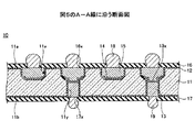
始めに、第1の実施の形態に係る配線基板の構造について説明する。図5は、第1の実施の形態に係る配線基板を例示する平面図である。図6は、図5のA−A線に沿う断面図である。図7は、図6の溝近傍の部分拡大図である。なお、説明の便宜のため、図5において、第2絶縁層16及び第1外部接続端子18は省略されている。
<First Embodiment>
[Structure of Wiring Board According to First Embodiment]
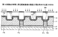
First, the structure of the wiring board according to the first embodiment will be described. FIG. 5 is a plan view illustrating the wiring substrate according to the first embodiment. 6 is a cross-sectional view taken along line AA in FIG. FIG. 7 is a partially enlarged view of the vicinity of the groove in FIG. For convenience of explanation, the second insulating
図5〜図7を参照するに、配線基板10は、基板本体11と、第1絶縁層12と、第1導電層13と、第2導電層14と、第3導電層15と、第2絶縁層16と、第3絶縁層17と、第1外部接続端子18と、第2外部接続端子19とを有する。
5 to 7, the
配線基板10において、基板本体11は、第1導電層13等を形成する基体となる部分であり、溝11x(所謂トレンチ)及び貫通孔11yが形成されている。基板本体11の厚さは、例えば、200〜400μm程度とすることができる。基板本体11の材料としては、シリコン、ガラス、セラミック等を用いることができる。
In the
なお、配線基板10は、半導体チップを搭載することにより半導体パッケージとなり得る。その際、半導体チップはシリコン基板を有するものが多いため、熱膨張係数を整合させる観点からすると、基板本体11の材料としてシリコンやシリコンに熱膨張係数が近い硼珪酸ガラスを用いると好適である。硼珪酸ガラスは、硼酸(B2O3)と珪酸(SiO2)を主成分として含むガラスであり、熱膨張係数は3ppm/℃程度である。又、加工性の観点からすると、基板本体11の材料としてシリコンを用いると好適である。
The
基板本体11の熱膨張係数を半導体チップの熱膨張係数と整合させる理由は、高温環境下や低温環境下で動作する場合も含め、配線基板10と半導体チップとの接合部に生じる熱応力を低減するためである。以下、基板本体11がシリコンである場合を例にして説明する。
The reason for matching the thermal expansion coefficient of the
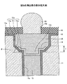
溝11xは、基板本体11の一方の面11a側に開口する溝であり、第3導電層15を含む配線パターンが形成される部分である。従って、溝11xは、配線パターンの形状に対応する位置に適宜形成される(図5参照)。溝11xの幅は、例えば50〜70μm程度とすることができる。溝11xの深さは、例えば40〜60μm程度とすることができる。溝11xの配設ピッチは、例えば80〜100μm程度とすることができる。
The
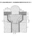
溝11xは、内底面11pと、内側面11qと、内底面11pの周縁部と内側面11qの一端部とを繋ぐ傾斜面11rとを有する。内底面11pと内側面11qとは略垂直であり、傾斜面11rは内底面11pに対して末広がりに傾斜している。換言すれば、内底面11pの周縁部と内側面11qの一端部(基板本体11の一方の面11aと反対側の端部)とが、内底面11pに対して末広がりに傾斜する傾斜面11rを介して連続し、溝11xを形成している。なお、『内側面11pに対して末広がりに傾斜する』とは、溝11xの開口端側の面積が内底面11pの面積よりも広くなるように、傾斜面11rが内底面11pに対して傾斜していることをいう。
The
傾斜面11rの高さT(基板本体11の厚さ方向の高さ)は、例えば、溝11xの幅(例えば50〜70μm程度)の10〜20%程度とすることができる。傾斜面11rの内底面11pに対する傾斜角θは、例えば、45〜55度程度とすることができる。なお、傾斜面11rの断面形状は直線でなくてもよく、曲線や、直線と曲線とを含む形状であってもよい。つまり、傾斜面11rは平面でもよく、曲面でもよく、平面と曲面の両方を含む形状であってもよい。
The height T of the
貫通孔11yは、一端が溝11xの内底面11pに連通し他端が基板本体11の他方の面11b側に開口する平面形状が略円形の孔(所謂TSV:through silicon via)である。貫通孔11yは、第1導電層13が形成される部分である。貫通孔11yの径は、例えば40〜60μm程度とすることができる。貫通孔11yの深さは、例えば140〜360μm程度とすることができる。このように、貫通孔11yは、比較的アスペクト比の高い孔である。なお、図6において、貫通孔11yと連通するように描かれていない溝11xも、断面図に表れない部分において、貫通孔11yと連通している(図5参照)。
The through-
第1絶縁層12は、基板本体11の一方の面11a及び他方の面11b、溝11xの内底面11p、内側面11q、及び傾斜面11r、並びに貫通孔11yの内側面に形成されている。第1絶縁層12は、基板本体11と第1導電層13、第2導電層14、及び第3導電層15との間を絶縁するための膜である。第1絶縁層12の材料としては、例えば、二酸化珪素(SiO2)や窒化珪素(SiN)、ポリイミド(PI)等を用いることができる。第1絶縁層12の厚さは、例えば1〜2μm程度とすることができる。なお、本実施の形態では、基板本体11がシリコン(半導体材料)であるから第1絶縁層12を設けているが、基板本体11がガラス等の絶縁性材料である場合には、第1絶縁層12を設けなくても構わない。
The first insulating
第1導電層13は、内側面が第1絶縁層12に被覆された貫通孔11yの少なくとも一部を充填するように形成されている。本実施の形態では、第1導電層13は、貫通孔11yの上部(溝11x側)を除く部分に充填されており、第1導電層13の上面(溝11x側の面)は、溝11xの内底面11pに対して基板本体11の他方の面11b側に窪んだ位置にある。つまり、第1導電層13の上面(溝11x側の面)と、貫通孔11yの内側面を被覆する第1絶縁層12とは凹部13xを形成している。
The first
なお、第1導電層13は、貫通孔11yの上部(溝11x側)も含めて、内側面が第1絶縁層12に被覆された貫通孔11yを完全に充填するように形成しても良い。その場合には、第1導電層13の上面(溝11x側の面)と溝11xの内底面11pを被覆する第1絶縁層12の上面とが略面一となり、凹部13xは形成されない。凹部13xの深さは、例えば0〜10μm程度とすることができる。
The first
但し、第1導電層13を、溝11xの内底面11pから突出するように形成することは好ましくない。第1導電層13が溝11xの内底面11pから突出すると、突出部を被覆する第2導電層14の被膜状態が悪化し、第2導電層14の剥離や断線等を引き起こす虞があるからである。本実施の形態では、このような問題の発生を回避するために、第1導電層13の上面(溝11x側の面)が溝11xの内底面11pに対して基板本体11の他方の面11b側に窪んだ位置に来る程度に第1導電層13を充填し、凹部13xを形成した場合を例にして説明する。
However, it is not preferable to form the first
第1導電層13の材料としては、例えば銅(Cu)等を用いることができる。第1導電層13は、第3導電層15を含む配線パターンを第2導電層14を介して第1外部接続端子18と電気的に接続する電極を構成している。
As a material of the first
第2導電層14は、凹部13x内及び溝11x内の一部に形成されている。より詳しくは、第2導電層14は、凹部13xが形成されない場合(第1導電層13の上面(溝11x側の面)と溝11xの内底面11pに形成された第1絶縁層12とが略面一となる場合)も含め、第1導電層13の上面(溝11x側の面)及び貫通孔11yの内側面を被覆する第1絶縁層12を被覆し、溝11xの内底面11pを被覆する第1絶縁層12の全部及び溝11xの傾斜面11rを被覆する第1絶縁層12の一部(溝11xの傾斜面11rの内側面11q側を除く部分)に延在している。つまり、第2導電層14は、溝11xの傾斜面11rを被覆する第1絶縁層12の外縁部上には形成されてなく、傾斜面11rの外縁部には第1絶縁層12が数μm程度の略一定幅で帯状に露出している。第2導電層14は、第1導電層13及び第3導電層15と電気的に接続されている。
The second
第2導電層14としては、例えばチタン(Ti)膜と銅(Cu)膜が第1導電層13又は第1絶縁層12上に、この順番で順次積層した導電層等を用いることができる。なお、チタン(Ti)膜は、第1絶縁層12の材料が二酸化珪素(SiO2)や窒化珪素(SiN)である場合に、密着性が良好である。第2導電層14の厚さは、例えば1μm程度とすることができる。
As the second
第3導電層15は、第2導電層14を被覆し、溝11xを充填するように形成されている。第3導電層15の上面は、基板本体11の一方の面11aを被覆する第1絶縁層12の上面と略面一とされている。第3導電層15の材料としては、例えば銅(Cu)等を用いることができる。第3導電層15は、配線パターンを構成している。第3導電層15の材料が銅(Cu)であり、第1絶縁層12の材料が二酸化珪素(SiO2)や窒化珪素(SiN)である場合には、両者は密着しない。しかしながら、第3導電層15は、第2導電層14を介して第1絶縁層12又は第1導電層13と密着するため、密着強度的には問題とならない。
The third
なお、本実施の形態では、第1導電層13と第3導電層15との間には、必ず第2導電層14が介在する構造となっている。これは、後述する配線基板10の製造工程から生じるものである。後述する配線基板10の製造工程により、第1導電層13及び第3導電層15にシームやボイド等の欠陥が発生することを防止することが可能となる。
In the present embodiment, the second
第2絶縁層16は、基板本体11の一方の面11aを被覆する第1絶縁層12上、及び溝11xから露出する第3導電層15上に形成されている。第2絶縁層16は開口部16xを有し、開口部16xの底部には第3導電層15の一部が露出している。開口部16xの底部に露出する第3導電層15は、第1外部接続端子18を形成する電極パッドとして機能する。第2絶縁層16の材料としては、例えばベンゾシクロブテン(BCB)、ポリベンゾオキサゾール(PBO)、ポリイミド(PI)等の絶縁性樹脂を用いることができる。第2絶縁層16の材料として、エポキシ系樹脂やイミド系樹脂等を含む感光性樹脂組成物等を用いても構わない。第2絶縁層16の厚さは、例えば5〜30μm程度とすることができる。
The second insulating
必要に応じ、開口部16xの底部に露出する第3導電層15上に、金属層を形成してもよい。金属層の例としては、Au層や、Ni/Au層(Ni層とAu層をこの順番で積層した金属層)、Ni/Pd/Au層(Ni層とPd層とAu層をこの順番で積層した金属層)等を挙げることができる。又、金属層の他の例としては、SnAgやSnAgCu等のはんだめっき等を挙げることができる。金属層を形成することにより、第3導電層15と第1外部接続端子18等との接続信頼性を向上できる。
If necessary, a metal layer may be formed on the third
第3絶縁層17は、基板本体11の他方の面11bを被覆する第1絶縁層12上、及び貫通孔11yから露出する第1導電層13上に形成されている。第3絶縁層17は開口部17xを有し、開口部17xの底部には第1導電層13の一部が露出している。開口部17xの底部に露出する第1導電層13は、第2外部接続端子19を形成する電極パッドとして機能する。第3絶縁層17の材料や厚さは、第2絶縁層16と同様であるため、その説明は省略する。
The third insulating
必要に応じ、開口部17xの底部に露出する第1導電層13上に、開口部16xの底部に露出する第3導電層15上に形成する金属層と同様な金属層を形成してもよい。金属層を形成することにより、第1導電層13と第2外部接続端子19等との接続信頼性を向上できる。
If necessary, a metal layer similar to the metal layer formed on the third
第1外部接続端子18は、開口部16xの底部に露出する第3導電層15上に(開口部16xの底部に露出する第3導電層15上に金属層が形成されている場合には、金属層上に)形成されている。第2外部接続端子19は、開口部17xの底部に露出する第1導電層13上に(開口部17xの底部に露出する第1導電層13上に金属層が形成されている場合には、金属層上に)形成されている。
The first
第1外部接続端子18及び第2外部接続端子19は、配線基板10と半導体チップや他の配線基板等とを電気的に接続するための端子である。第1外部接続端子18及び第2外部接続端子19としては、例えば、はんだバンプ等を用いることができる。第1外部接続端子18及び第2外部接続端子19がはんだバンプである場合の材料としては、例えばPbを含む合金、SnとCuの合金、SnとAgの合金、SnとAgとCuの合金等を用いることができる。
The first
なお、第2絶縁層16や第3絶縁層17上に、更に配線層と絶縁層とを交互に積層し、多層配線を形成しても構わない。
Note that a multilayer wiring may be formed by alternately stacking wiring layers and insulating layers on the second insulating
[第1の実施の形態に係る配線基板の製造方法]
次に、第1の実施の形態に係る配線基板の製造方法について説明する。図8〜図22は、第1の実施の形態に係る配線基板の製造工程を例示する図である。
[Method for Manufacturing Wiring Board According to First Embodiment]
Next, a method for manufacturing a wiring board according to the first embodiment will be described. 8 to 22 are diagrams illustrating the manufacturing process of the wiring board according to the first embodiment.
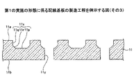
始めに、図8に示す工程では、基板本体11を準備し、基板本体11の一方の面11a側に、最終的に溝11xの一部となる溝11mを形成する。溝11mは断面形状が略逆台形状の溝であり、溝11mの側壁の傾斜面は最終的に溝11xの傾斜面11rとなる。溝11xは、第3導電層15を含む配線パターンが形成される部分である。従って、最終的に溝11xの一部となる溝11mは、配線パターンの形状に対応する位置に適宜形成される。基板本体11は、例えば6インチ(約150mm)、8インチ(約200mm)、12インチ(約300mm)等のシリコンウェハ等である。シリコンウェハの厚さは、例えば0.625mm(6インチの場合)、0.725mm(8インチの場合)、0.775mm(12インチの場合)等であるが、バックサイドグラインダー等で適宜薄型化することができる。
First, in the process shown in FIG. 8, the
溝11mは、例えば、結晶方位(100)又は(110)からなるシリコンウェハにおいて、結晶方位(100)又は(110)に対して垂直又は平行にエッチングすることにより形成できる。以下に一例を挙げる。 The groove 11m can be formed, for example, by etching a silicon wafer having a crystal orientation (100) or (110) perpendicularly or parallel to the crystal orientation (100) or (110). An example is given below.
溝11mは、例えば、基板本体11の一方の面11aに溝11mを形成する位置を開口するレジスト層(図示せず)を形成し、レジスト層(図示せず)をマスクとして基板本体11をエッチングすることにより形成できる。例えば、基板本体11の一方の面11aをシリコンの(100)面とし、例えばKOH(水酸化カリウム)やTMAH(テトラメチルアンモニウムハイドロオキサイド)等のアルカリ性溶液を用いた結晶異方性エッチング法でシリコンの(100)面をエッチングすることにより、溝11mを形成できる。
The groove 11m is formed, for example, by forming a resist layer (not shown) that opens a position where the groove 11m is formed on one
すなわち、シリコンの(111)面のエッチングレートはシリコンの(100)面のエッチングレートと比較すると著しく遅いため、シリコンの(100)面からKOH(水酸化カリウム)やTMAH(テトラメチルアンモニウムハイドロオキサイド)等によりエッチングを行うと、エッチングレートの遅い(111)面(傾斜面11rに対応)が現れて、断面形状が略逆台形状の溝11mが形成される。
That is, since the etching rate of the (111) plane of silicon is significantly slower than the etching rate of the (100) plane of silicon, KOH (potassium hydroxide) or TMAH (tetramethylammonium hydroxide) from the (100) plane of silicon. When etching is performed by, for example, a (111) plane having a slow etching rate (corresponding to the
溝11mの幅は、例えば50〜70μm程度とすることができる。溝11mの高さT(基板本体11の厚さ方向の高さ)は、例えば、溝11mの幅(例えば50〜70μm程度)の10〜20%程度とすることができる。溝11mの配設ピッチは、例えば80〜100μm程度とすることができる。なお、この例では、傾斜面の内底面に対する傾斜角θは54.7度となるが、基板本体11の一方の面11aをシリコンの(110)面とした場合には、傾斜面の内底面に対する傾斜角θは45度となる。
The width of the groove 11m can be, for example, about 50 to 70 μm. The height T of the groove 11m (the height in the thickness direction of the substrate body 11) can be, for example, about 10 to 20% of the width (for example, about 50 to 70 μm) of the groove 11m. The arrangement pitch of the grooves 11m can be set to about 80 to 100 μm, for example. In this example, the inclination angle θ with respect to the inner bottom surface of the inclined surface is 54.7 degrees. However, when one
次いで、図9に示す工程では、溝11m内を更に加工し、内底面11p、内側面11q、及び内底面11pの周縁部と内側面11qの一端部とを繋ぐ傾斜面11rを有する溝11xを完成させる。溝11xは、例えば、図8のレジスト層(図示せず)を除去していない状態で、レジスト層(図示せず)をマスクとして基板本体11(溝11m内)を更にエッチングすることにより形成できる。エッチングとしては、例えばSF6(六フッ化硫黄)を用いた反応性イオンエッチング(DRIE:Deep Reactive Ion Etching)等の異方性エッチング法を用いると好適である。溝11xの深さ(基板本体11の一方の面11aと内底面11pとの距離)は、例えば40〜60μm程度とすることができる。なお、傾斜面11rの断面形状は直線でなくてもよく、曲線や、直線と曲線とを含む形状であってもよい。
Next, in the process shown in FIG. 9, the inside of the groove 11m is further processed to form a
次いで、図10に示す工程では、一端が基板本体11の一方の面11a側に形成された溝11xに連通し、他端が基板本体11の他方の面11b側に開口する貫通孔11yを形成する。貫通孔11yは、例えば、貫通孔11yを形成する位置を開口するレジスト層(図示せず)を形成し、レジスト層(図示せず)をマスクとして基板本体11をエッチングすることにより形成できる。エッチングとしては、例えばSF6(六フッ化硫黄)を用いた反応性イオンエッチング(DRIE:Deep Reactive Ion Etching)等の異方性エッチング法を用いると好適である。貫通孔11yの平面形状は、例えば略円形とすることができる。貫通孔11yの径は、例えば40〜60μm程度とすることができる。貫通孔11yの深さは、例えば140〜360μm程度とすることができる。なお、図9に示す工程と図10に示す工程との間に、基板本体11の一方の面11a並びに溝11xの内底面11p、内側面11q、及び傾斜面11rを被覆する熱酸化膜(SiO2)を形成する工程を設けても良い。
Next, in the step shown in FIG. 10, one end communicates with a
次いで、図11に示す工程では、基板本体11の一方の面11a及び他方の面11b、溝11xの内底面11p、内側面11q、及び傾斜面11r、並びに貫通孔11yの内側面に第1絶縁層12を形成する。第1絶縁層12としては、例えば熱酸化膜(SiO2)を用いることができる。第1絶縁層12は、基板本体11の表面近傍の温度を例えば1000℃以上とするウェット熱酸化法により熱酸化することで形成できる。第1絶縁層12の厚さは、例えば1〜2μm程度とすることができる。なお、第1絶縁層12として、CVD(Chemical Vapor Deposition)法等により、例えば二酸化珪素(SiO2)や窒化珪素(SiN)、ポリイミド(PI)等の膜を形成しても構わない。なお、図9に示す工程と図10に示す工程との間に、前述の熱酸化膜(SiO2)を形成する工程を設けた場合には、設けた熱酸化膜(SiO2)を図11に示す工程の前に一端除去してから、図11に示す工程で改めて第1絶縁層12を形成する。
Next, in the step shown in FIG. 11, the first insulation is formed on the one
次いで、図12に示す工程では、基板本体11の他方の面11bを被覆する第1絶縁層12上に、接着層21を介して金属層22を配設する。そして、内側面が第1絶縁層12に被覆された貫通孔11yに対応する部分の接着層21をアッシング法等により除去し、開口部21xを形成する。これにより、内側面が第1絶縁層12に被覆された貫通孔11yの底部に金属層22の上面が露出する。金属層22は、電解めっき法により、第1導電層13等を形成する際の給電層となる部材である。金属層22としては、例えば銅(Cu)板や銅(Cu)箔等を用いることができる。以下、金属層22が銅(Cu)板である場合を例にして説明する。
Next, in the step shown in FIG. 12, the
次いで、図13に示す工程では、金属層22を給電層とする電解めっき法により、金属層22側から貫通孔11y内にめっき膜を析出成長させることで、貫通孔11yの少なくとも一部を充填する第1導電層13Sを形成する。なお、第1導電層13Sは、不要部分が除去されて、最終的には第1導電層13となる層である。第1導電層13Sの材料としては、例えば銅(Cu)等を用いることができる。第1導電層13Sは、貫通孔11yの上部(溝11x側)を除く部分を充填すれば十分である。この場合、第1導電層13Sの上面(溝11x側の面)と、貫通孔11yの内側面を被覆する第1絶縁層12とにより凹部13xが形成される。
Next, in the step shown in FIG. 13, at least a part of the through
なお、前述のように、第1導電層13Sは、貫通孔11yの上部(溝11x側)も含めて、内側面が第1絶縁層12に被覆された貫通孔11yを完全に充填するよう(第1導電層13Sの上面(溝11x側の面)と溝11xの内底面11pに形成された第1絶縁層12とが略面一となるよう)に形成しても良いが、第1導電層13Sを溝11xの内底面11pから突出するように形成することは好ましくない。凹部13xの深さは、例えば0〜10μm程度とすることができる。
As described above, the first
貫通孔11yの内側面は第1絶縁層12に被覆されているため、金属層22側からのみ(一方向からのみ)めっき膜が成長して第1導電層13Sが形成される。これにより、第1導電層13Sに、従来の配線基板100のように二方向からめっき膜が成長することに起因してシームやボイド等の欠陥が発生することを防止できる。その結果、第1導電層13Sがシームやボイド等の欠陥の発生に起因して熱応力により断線したり、第2外部接続端子19との接続信頼性が低下したりする問題を回避できる。
Since the inner surface of the through-
次いで、図14に示す工程では、基板本体11の一方の面11aを被覆する第1絶縁層12上、溝11xの内底面11p、内側面11q、及び傾斜面11rを被覆する第1絶縁層12上、並びに凹部13x内に、例えばスパッタ法等により第2導電層14Sを形成する。なお、第2導電層14Sは、不要部分が除去されて、最終的には第2導電層14となる層である。第2導電層14Sとしては、例えばチタン(Ti)膜と銅(Cu)膜が第1絶縁層12上又は第1導電層13上に、この順番で順次積層した導電層等を用いることができる。第2導電層14Sの厚さは、例えば1μm程度とすることができる。
Next, in the process shown in FIG. 14, the first insulating
次いで、図15に示す工程では、第2導電層14Sを被覆するレジスト層23Sを形成する。なお、レジスト層23Sは、不要部分が除去されて、最終的にはレジスト層23となる層である。具体的には、第2導電層14S上に、例えばエポキシ系樹脂やイミド系樹脂等を含む感光性樹脂組成物からなる液状又はペースト状のレジストを塗布する。或いは、第2導電層14S上に、例えばエポキシ系樹脂やイミド系樹脂等を含む感光性樹脂組成物からなるフィルム状のレジスト(例えば、ドライフィルムレジスト等)をラミネートする。レジスト層23Sの厚さは、例えば数μm程度とすることができる。なお、ここでは、レジスト層23Sがポジ型レジストである場合を例にして以下の説明を行うが、レジスト層23Sとしてネガ型レジストを用いても構わない。
Next, in a step shown in FIG. 15, a resist
次いで、図16に示す工程では、遮光部24aを有するマスク24を介してレジスト層23Sを矢印方向から露光する。本実施の形態では、基板本体11の一方の面11a上に形成されたレジスト層23S、溝11xの内側面11q上、及び溝11xの傾斜面11rの一部の上に形成されたレジスト層23Sを露光するように、遮光部24aが形成されている。
Next, in the step shown in FIG. 16, the resist
次いで、図17に示す工程では、露光されたレジスト層23Sを現像し、基板本体11の一方の面11a上に形成されたレジスト層23S、溝11xの内側面11q上、及び溝11xの傾斜面11rの一部の上に形成されたレジスト層23Sを除去する。これにより、溝11xの内底面11p上及び傾斜面11rの外縁部(内側面11q側)を除く部分にレジスト層23が形成される。つまり、レジスト層23は、溝11xの傾斜面11rを被覆する第1絶縁層12の外縁部上には形成されず、傾斜面11rの外縁部には第1絶縁層12が数μm程度の略一定幅で帯状に露出する。
Next, in the step shown in FIG. 17, the exposed resist
次いで、図18に示す工程では、レジスト層23をマスクとして図17に示す第2導電層14Sをエッチングし、レジスト層23に被覆されていない第2導電層14Sを除去する。これにより、レジスト層23に被覆された第2導電層14が形成される。次いで、図19に示す工程では、レジスト層23を除去する。
Next, in the step shown in FIG. 18, the second
次いで、図20に示す工程では、金属層22、第1導電層13S、及び第2導電層14を給電層とする電解めっき法により、溝11x内に第2導電層14側からめっき膜を析出成長させることで、第3導電層15Sを形成する。なお、第3導電層15Sは、不要部分が除去されて、最終的には第3導電層15となる層である。第3導電層15Sの材料としては、例えば銅(Cu)等を用いることができる。第3導電層15Sは、基板本体11の一方の面11aを被覆する第1絶縁層12の上面から突出するように形成する。第3導電層15Sの第1絶縁層12の上面からの突出量は、例えば30〜40μm程度とすることができる。
Next, in the process shown in FIG. 20, a plating film is deposited from the second
次いで、図21に示す工程では、CMP(Chemical Mechanical Polishing)法等により、基板本体11の一方の面11a側から突出する第3導電層15S(図20参照)を研磨し、第3導電層15を形成する。第3導電層15の上面は、基板本体11の一方の面11aを被覆する第1絶縁層12の上面と略面一となる。この工程により、第3導電層15を含んで構成される配線パターンが形成される。
Next, in the step shown in FIG. 21, the third
次いで、図22に示す工程では、図21に示す接着層21及び金属層22を除去し、更に、基板本体11の他方の面11b側から突出する第1導電層13S(図21参照)を研磨し、第1導電層13を形成する。銅(Cu)板である金属層22は、例えば塩化第二鉄水溶液や塩化第二銅水溶液、過硫酸アンモニウム水溶液等を用いたウェットエッチングにより除去できる。但し、第3導電層15が銅(Cu)から構成されている場合には、第3導電層15の露出面が金属層22とともにエッチングされることを防止するため、第3導電層15の露出面をマスクする必要がある。接着層21は、アッシング法等により除去できる。第1導電層13Sは、CMP(Chemical Mechanical Polishing)法等により研磨できる。第1導電層13の下面(溝11x側の面と反対の面)は、基板本体11の他方の面11bを被覆する第1絶縁層12の下面と略面一となる。
Next, in the step shown in FIG. 22, the
次いで、図22に示す工程の後、周知の方法により、開口部16xを有する第2絶縁層16、開口部17xを有する第3絶縁層17、第1外部接続端子18、及び第2外部接続端子19を形成することにより、図5〜図7に示す配線基板10が完成する。
Next, after the step shown in FIG. 22, by a well-known method, the second insulating
ここで、比較例を参照しながら、第1の実施の形態に係る配線基板10の有する特有の効果について説明する。図23及び図24は、比較例1に係る配線基板の製造工程を例示する図である。始めに、図23に示す工程では、第1の実施の形態の図9〜図17と同様の工程を実行する。つまり、図8に示す傾斜面11rを形成する工程は実行していないため、図23に示すような断面形状が矩形状の溝11jが形成され、溝11jの内底面及び内側面の下端部(内底面側)を被覆するレジスト層23Aが形成される。
Here, with reference to a comparative example, a specific effect of the
次いで、図24に示す工程では、第1の実施の形態の図18及び図19と同様の工程を実行し、第2導電層14Aを形成する。第2導電層14Aは、凹部13x内及び溝11j内の一部に形成されている。より詳しくは、第2導電層14Aは、第1導電層13の上面(溝11j側の面)を被覆し、溝11jの内底面を被覆する第1絶縁層12の全部及び溝11jの内側面を被覆する第1絶縁層12の下端部(溝11jの内底面側)に延在している。なお、第2導電層14Aの材料や厚さは、第2導電層14と同様である。
Next, in the step shown in FIG. 24, the same steps as those in FIGS. 18 and 19 of the first embodiment are executed to form the second
このように、図8に示す傾斜面11rを形成する工程を実行しないと、溝11jの内側面を被覆する第1絶縁層12の下端部(溝11jの内底面側)にも第2導電層14Aが形成されてしまう。その結果、金属層22、第1導電層13S、及び第2導電層14Aを給電層とする電解めっき法により、溝11j内に第2導電層14A側からめっき膜を析出成長させて凹部13x及び溝11jを充填すると、二方向(溝11jの内底面及び内側面の下端部)から成長してきためっき膜同士の接合部にシームやボイド等の欠陥が発生する虞が生じる。
Thus, if the step of forming the
なお、比較例1において、図15に相当する工程では、断面形状が矩形状の溝11jの角部にレジスト層23Aが溜まりやすいため、角部に形成されるレジスト層23Aは他の部分に比べて厚くなりやすい。そのため、図16に相当する工程で、角部に形成されたレジスト層23Aを露光及び現像しても、角部に形成されたレジスト層23Aを完全に除去できない場合がある。従って、断面形状が矩形状の溝11jの内側面の下端部(内底面側)がレジスト層23Aで被覆されないようにする事は、極めて困難である。
In Comparative Example 1, in the process corresponding to FIG. 15, the resist
一方、第1の実施の形態に係る配線基板10の製造方法では、図8に示す工程により傾斜面11rを形成するため、傾斜面11rを被覆する第1絶縁層12の一部には第2導電層14が形成されるが、内側面11pを被覆する第1絶縁層12には第2導電層14が全く形成されない。その結果、金属層22、第1導電層13S、及び第2導電層14を給電層とする電解めっき法により、溝11x内に第2導電層14側からめっき膜を析出成長させて凹部13x及び溝11xを充填する第3導電層15Sを形成する際に、内側面11qの方向からはめっき膜が成長しないため、シームやボイド等の欠陥が発生する虞を低減できる。その結果、第3導電層15Sがシームやボイド等の欠陥の発生に起因して熱応力により断線したり、第1外部接続端子18との接続信頼性が低下したりする問題を回避できる。
On the other hand, in the method of manufacturing the
なお、第2導電層14は傾斜面11rの一部(内底面11p側)にも形成されており、ここからもめっき膜が成長するが、傾斜面11rは内底面11pに対して例えば45〜55度程度傾斜しているため、内底面11pに対して略垂直の内側面11qに第2導電層14が形成された場合と比較して、シームやボイド等の欠陥が発生する虞を大幅に低減できる。
Note that the second
図25は、比較例2に係る配線基板を例示する断面図である。図25を参照するに、配線基板10Aにおいて、溝11kは、基板本体11の一方の面11a側に開口する断面がテーパ形状の溝である。つまり、溝11kの基板本体11の一方の面11a側に開口する開口部の幅は内底面の幅よりも広い。溝11kのような断面がテーパ形状の溝の場合には、図25に示すように傾斜面の一部に第2導電層14Bが形成されると、ここからもめっき膜が成長するが、内底面に対して略垂直の内側面に第2導電層が形成された場合と比較すると、シームやボイド等の欠陥が発生する虞を低減できる。
FIG. 25 is a cross-sectional view illustrating a wiring board according to Comparative Example 2. Referring to FIG. 25, in wiring
しかしながら、溝11kのような断面がテーパ形状の溝を形成すると、溝11kを狭ピッチで配設することができない。つまり、配線パターンの狭ピッチ化の妨げになる。一方、第1の実施の形態に係る配線基板10では、傾斜面11rは、内側面11qの下端部(内底面11p側)のみに形成されているため、溝11xを狭ピッチで配設することができる。つまり、傾斜面11rを形成することは、配線パターンの狭ピッチ化の妨げにはならない。
However, if a groove having a tapered cross section such as the
このように、第1の実施の形態によれば、基板本体11の他方の面11bに接着層21を介して金属層22を配設する。そして、金属層22をめっき給電層に利用した電解めっき法により、内側面を第1絶縁層12で被覆した貫通孔11y内に一方向のみからめっき膜を成長させて第1導電層13を形成する。その結果、第1導電層13にシームやボイド等の欠陥が発生することを防止することが可能となり、第1導電層13がシームやボイド等の欠陥の発生に起因して熱応力により断線したり、第2外部接続端子19との接続信頼性が低下したりする問題を回避できる。
Thus, according to the first embodiment, the
又、第1導電層13の上面(溝11x側の面)及び貫通孔11yの内側面を被覆する第1絶縁層12を被覆し、溝11xの内底面11pを被覆する第1絶縁層12及び溝11xの傾斜面11rを被覆する第1絶縁層12の一部(溝11xの傾斜面11rの内側面11q側を除く部分)に延在する第2導電層14を形成する。そして、金属層22、第1導電層13、及び第2導電層14をめっき給電層に利用した電解めっき法により、凹部13x内及び溝11x内に実質的に一方向のみからめっき膜を成長させて第3導電層15を形成する。その結果、第3導電層15にシームやボイド等の欠陥が発生することを防止することが可能となり、第3導電層15がシームやボイド等の欠陥の発生に起因して熱応力により断線したり、第1外部接続端子18との接続信頼性が低下したりする問題を回避できる。
Further, the first insulating
又、傾斜面11rを有する溝11xは、断面形状が略矩形状の溝(図1の溝110x等)と比較すると、基板本体11の溝11x周辺部にかかる応力を緩和する効果がある。
Further, the
なお、本実施の形態では、前述の製造工程により配線基板を作製するため、第1導電層13と第3導電層15との間には、必ず第2導電層14が介在する構造となる(図6等参照)。
In the present embodiment, since the wiring substrate is manufactured by the above-described manufacturing process, the second
〈第1の実施の形態の変形例1〉
第1の実施の形態の変形例1では、第1の実施の形態とは第2導電層14の形成位置が異なる例を示す。なお、第1の実施の形態の変形例1において、既に説明した実施の形態と同一構成部品についての説明は省略する。
<
The first modification of the first embodiment shows an example in which the formation position of the second
図26及び図27は、第1の実施の形態の変形例1に係る配線基板の溝近傍の部分拡大図である。 26 and 27 are partially enlarged views of the vicinity of the groove of the wiring board according to the first modification of the first embodiment.
図26に示すように、第2導電層14は、第1導電層13の溝11x側の面を被覆し、溝11x内の内底面11pを被覆する第1絶縁層12上の全部に延在するように形成してもよい。つまり、溝11x内において、第2導電層14は、傾斜面11rを被覆する第1絶縁層12上には形成しなくてもよい。更に、第2導電層14は、第1導電層13の溝11x側の面を被覆し、溝11x内の内底面11pを被覆する第1絶縁層12上の大部分(外縁部を除く部分等)に延在するように形成してもよい。第2導電層14を内底面11pを被覆する第1絶縁層12上の全部に形成しなくても、内底面11pを被覆する第1絶縁層12上の一部分(内底面11pの外縁部を除く部分等)に形成すれば、第2導電層14等を給電層とする電解めっき法により、第3導電層15を形成できるからである。
As shown in FIG. 26, the second
又、図27に示すように、第2導電層14は、第1導電層13の溝11x側の面を被覆し、溝11x内の内底面11pを被覆する第1絶縁層12上の全部、及び傾斜面11rを被覆する第1絶縁層12上の全部に延在するように形成してもよい。この場合にも、第2導電層14等を給電層とする電解めっき法により第3導電層15を形成する際に、内側面11q側からめっき膜が成長することがないため、第3導電層15にシームやボイド等の欠陥が発生することを防止できる。
As shown in FIG. 27, the second
このように、第2導電層14は、溝11x内の内側面11qを除く部分の少なくとも一部に延在してれば、第2導電層14等を給電層とする電解めっき法により第3導電層15を形成する際に、シームやボイド等の欠陥が発生することを防止できる。
As described above, if the second
〈第1の実施の形態の変形例2〉
第1の実施の形態の変形例2では、第1の実施の形態とは出荷形態の異なる配線基板を例示する。なお、第1の実施の形態の変形例2において、既に説明した実施の形態と同一構成部品についての説明は省略する。
<Modification 2 of the first embodiment>
In the second modification of the first embodiment, a wiring board having a different shipping form from the first embodiment is illustrated. In the second modification of the first embodiment, the description of the same components as those of the already described embodiment is omitted.
図28は、第1の実施の形態の変形例2に係る配線基板を例示する断面図である。図28を参照するに、配線基板10Aは、配線基板10(図6等参照)から第2絶縁層16、第3絶縁層17、第1外部接続端子18、及び第2外部接続端子19が削除されたものである。
FIG. 28 is a cross-sectional view illustrating a wiring board according to Modification 2 of the first embodiment. Referring to FIG. 28, the
図6等に示す配線基板10は第2絶縁層16及び第3絶縁層17を有していたが、第2絶縁層16及び第3絶縁層17はソルダーレジスト層として機能する絶縁層であり必須の構成要素ではないため、図28に示す配線基板10Aのように第2絶縁層16及び第3絶縁層17を有さなくても構わない。
The
又、図6等に示す配線基板10は第1外部接続端子18及び第2外部接続端子19を有していたが、第1外部接続端子18及び第2外部接続端子19は配線基板10と半導体チップや他の配線基板等とを電気的に接続するための端子であり必須の構成要素ではないため、図28に示す配線基板10Aのように第1外部接続端子18及び第2外部接続端子19を有さなくても構わない。配線基板10Aでは、基板本体11の一方の面11a側に露出する第3導電層15や、基板本体11の他方の面11b側に露出する第1導電層13自体が外部接続端子として機能する。
6 has the first
配線基板10Aを半導体チップや他の配線基板等と接続する場合には、基板本体11の一方の面11a側に露出する第3導電層15や、基板本体11の他方の面11b側に露出する第1導電層13を、配線基板10Aと接続される半導体チップや他の配線基板側に設けられたバンプやピン等と接続すればよい。
When the
このように、配線基板の出荷形態は、図6等に示す形態には限定されず、図28に示す形態としてもよい。又、これ以外の形態としてもよい。一例を挙げれば配線基板10Aに第2絶縁層16及び第3絶縁層17のみを形成した形態(第1外部接続端子18及び第2外部接続端子19は形成しない)や、基板本体11の一方の面11a側及び他方の面11b側の何れか一方のみに絶縁層や外部接続端子を形成した形態等である。
Thus, the shipment form of the wiring board is not limited to the form shown in FIG. 6 and the like, and may be the form shown in FIG. Moreover, it is good also as forms other than this. For example, a configuration in which only the second insulating
以上、好ましい実施の形態及びその変形例について詳説したが、上述した実施の形態及びその変形例に制限されることはなく、特許請求の範囲に記載された範囲を逸脱することなく、上述した実施の形態及びその変形例に種々の変形及び置換を加えることができる。 The preferred embodiment and its modification have been described in detail above, but the present invention is not limited to the above-described embodiment and its modification, and the above-described implementation is performed without departing from the scope described in the claims. Various modifications and substitutions can be added to the embodiment and its modifications.
例えば、配線基板10等は、基板本体11に先に貫通孔11yを形成し、その後、溝11xを形成する工程により製造してもよい。
For example, the
10、10A、10B 配線基板
11 基板本体
11a 基板本体の一方の面
11b 基板本体の他方の面
11j、11k、11m、11x 溝
11p 内底面
11q 内側面
11r 傾斜面
11y 貫通孔
12 第1絶縁層
13、13S 第1導電層
13x 凹部
14、14A、14B、14S 第2導電層
15、15S 第3導電層
16 第2絶縁層
16x、17x、21x 開口部
17 第3絶縁層
18 第1外部接続端子
19 第2外部接続端子
21 接着層
22 金属板
23、23A、23S レジスト層
24 マスク
24a 遮光部
T 高さ
θ 角度
10, 10A,
Claims (13)
前記基板本体の一方の面側に開口する溝であって、内底面の周縁部と内側面の一端部とが、前記内底面に対して末広がりに傾斜する傾斜面を介して連続する溝と、
一端が前記内底面に連通し、他端が前記基板本体の他方の面側に開口する貫通孔と、
前記他端側から前記貫通孔の少なくとも一部を充填する第1導電層と、
前記第1導電層の前記溝側の面を被覆し、前記溝内の前記内側面を除く部分の少なくとも一部に延在する第2導電層と、
前記第2導電層を被覆し、前記溝を充填する第3導電層と、を有する配線基板。 A substrate body;
A groove that opens to one surface side of the substrate body, the peripheral edge portion of the inner bottom surface and one end portion of the inner side surface continuing through an inclined surface that is inclined toward the end with respect to the inner bottom surface;
A through hole having one end communicating with the inner bottom surface and the other end opening on the other surface side of the substrate body;
A first conductive layer filling at least part of the through hole from the other end side;
A second conductive layer covering a surface of the first conductive layer on the groove side and extending to at least a part of a portion excluding the inner surface in the groove;
And a third conductive layer covering the second conductive layer and filling the groove.
前記基板本体に、一端が前記内底面に連通し、他端が前記基板本体の他方の面側に開口する貫通孔を形成する第2工程と、
前記基板本体の前記他方の面に金属層を形成する第3工程と、
前記金属層を給電層とする電解めっき法により、前記他端側から前記貫通孔の少なくとも一部を充填する第1導電層を形成する第4工程と、
前記第1導電層の前記溝側の面を被覆し、前記溝内の前記内側面を除く部分の少なくとも一部に延在する第2導電層を形成する第5工程と、
前記金属層、前記第1導電層、及び前記第2導電層を給電層とする電解めっき法により、前記第2導電層を被覆し、前記溝を充填する第3導電層を形成する第6工程と、
前記金属層を除去する第7工程と、を有する配線基板の製造方法。 A groove that opens on one surface side of the substrate body, and a peripheral edge portion of the inner bottom surface and one end portion of the inner surface are continuously connected to the substrate body via an inclined surface that inclines toward the inner bottom surface. A first step of forming a groove to be
A second step of forming, in the substrate body, a through hole having one end communicating with the inner bottom surface and the other end opened on the other surface side of the substrate body;
A third step of forming a metal layer on the other surface of the substrate body;
A fourth step of forming a first conductive layer filling at least a part of the through hole from the other end side by an electrolytic plating method using the metal layer as a power feeding layer;
A fifth step of forming a second conductive layer covering the groove side surface of the first conductive layer and extending to at least a part of a portion excluding the inner side surface in the groove;
A sixth step of forming a third conductive layer covering the second conductive layer and filling the groove by an electrolytic plating method using the metal layer, the first conductive layer, and the second conductive layer as a power feeding layer When,
And a seventh step of removing the metal layer.
前記基板本体の一方の面は、前記シリコンの(100)面又は(110)面である請求項9乃至12の何れか一項記載の配線基板の製造方法。 The substrate body is made of silicon,
One surface of the substrate body, a manufacturing method of a wiring board of any one of claims 9 to 12, wherein a (100) plane or (110) plane of silicon.
Priority Applications (2)
| Application Number | Priority Date | Filing Date | Title |
|---|---|---|---|
| JP2011119619A JP5613620B2 (en) | 2011-05-27 | 2011-05-27 | Wiring board and manufacturing method thereof |
| US13/480,985 US8729407B2 (en) | 2011-05-27 | 2012-05-25 | Wiring substrate and method for manufacturing wiring substrate |
Applications Claiming Priority (1)
| Application Number | Priority Date | Filing Date | Title |
|---|---|---|---|
| JP2011119619A JP5613620B2 (en) | 2011-05-27 | 2011-05-27 | Wiring board and manufacturing method thereof |
Publications (3)
| Publication Number | Publication Date |
|---|---|
| JP2012248703A JP2012248703A (en) | 2012-12-13 |
| JP2012248703A5 JP2012248703A5 (en) | 2014-04-24 |
| JP5613620B2 true JP5613620B2 (en) | 2014-10-29 |
Family
ID=47218463
Family Applications (1)
| Application Number | Title | Priority Date | Filing Date |
|---|---|---|---|
| JP2011119619A Active JP5613620B2 (en) | 2011-05-27 | 2011-05-27 | Wiring board and manufacturing method thereof |
Country Status (2)
| Country | Link |
|---|---|
| US (1) | US8729407B2 (en) |
| JP (1) | JP5613620B2 (en) |
Families Citing this family (16)
| Publication number | Priority date | Publication date | Assignee | Title |
|---|---|---|---|---|
| US8304863B2 (en) * | 2010-02-09 | 2012-11-06 | International Business Machines Corporation | Electromigration immune through-substrate vias |
| US20140306349A1 (en) * | 2013-04-11 | 2014-10-16 | Qualcomm Incorporated | Low cost interposer comprising an oxidation layer |
| JP2014236102A (en) * | 2013-05-31 | 2014-12-15 | 凸版印刷株式会社 | Wiring board with through electrode, manufacturing method of the same, and semiconductor device |
| JP6286169B2 (en) * | 2013-09-26 | 2018-02-28 | 新光電気工業株式会社 | Wiring board and manufacturing method thereof |
| US10777839B2 (en) * | 2014-03-28 | 2020-09-15 | Infineon Technologies Ag | Method for forming a battery element, a battery element and a battery |
| TWI553804B (en) * | 2014-06-06 | 2016-10-11 | 矽品精密工業股份有限公司 | Substrate structure and method of manufacture thereof |
| KR102211741B1 (en) * | 2014-07-21 | 2021-02-03 | 삼성전기주식회사 | Printed circuit board and method of manufacturing the same |
| JP2016213283A (en) * | 2015-05-01 | 2016-12-15 | ソニー株式会社 | Manufacturing method and wiring board with through electrode |
| EP3109199B1 (en) * | 2015-06-25 | 2022-05-11 | Nivarox-FAR S.A. | Silicon-based part with at least one chamfer and method for manufacturing same |
| TWI625991B (en) * | 2016-10-17 | 2018-06-01 | 南亞電路板股份有限公司 | Circuit board structure and method for forming the same |
| JP7230462B2 (en) * | 2017-12-04 | 2023-03-01 | ローム株式会社 | Semiconductor device and its manufacturing method |
| WO2019171470A1 (en) * | 2018-03-06 | 2019-09-12 | 株式会社 東芝 | Capacitor and method for producing same |
| CN111508893B (en) * | 2019-01-31 | 2023-12-15 | 奥特斯(中国)有限公司 | Component carrier and method for producing a component carrier |
| CN112956284B (en) * | 2019-08-22 | 2023-04-14 | 宏启胜精密电子(秦皇岛)有限公司 | Transparent circuit board and method for manufacturing same |
| WO2021155222A1 (en) * | 2020-01-31 | 2021-08-05 | Ttm Technologies Inc. | Printed circuit board assemblies with engineered thermal paths and methods of manufacturing |
| US11901266B2 (en) * | 2021-08-30 | 2024-02-13 | Taiwan Semiconductor Manufacturing Company, Ltd. | Semiconductor device structure and method for forming the same |
Family Cites Families (10)
| Publication number | Priority date | Publication date | Assignee | Title |
|---|---|---|---|---|
| JP4340832B2 (en) * | 2001-05-10 | 2009-10-07 | 日立電線株式会社 | Wiring board and manufacturing method thereof |
| JP2003318178A (en) * | 2002-04-24 | 2003-11-07 | Seiko Epson Corp | Semiconductor device, its manufacturing method, circuit board, and electronic apparatus |
| JP4056854B2 (en) | 2002-11-05 | 2008-03-05 | 新光電気工業株式会社 | Manufacturing method of semiconductor device |
| US7088003B2 (en) * | 2004-02-19 | 2006-08-08 | International Business Machines Corporation | Structures and methods for integration of ultralow-k dielectrics with improved reliability |
| JP5038612B2 (en) * | 2005-09-29 | 2012-10-03 | 富士通セミコンダクター株式会社 | Semiconductor device |
| JP5154789B2 (en) * | 2006-12-21 | 2013-02-27 | ルネサスエレクトロニクス株式会社 | Semiconductor device and manufacturing method of semiconductor device |
| US8334202B2 (en) * | 2009-11-03 | 2012-12-18 | Infineon Technologies Ag | Device fabricated using an electroplating process |
| KR20120048991A (en) * | 2010-11-08 | 2012-05-16 | 삼성전자주식회사 | Semiconductor devices and methods of fabricating the same |
| US9018094B2 (en) * | 2011-03-07 | 2015-04-28 | Invensas Corporation | Substrates with through vias with conductive features for connection to integrated circuit elements, and methods for forming through vias in substrates |
| JP2013105753A (en) * | 2011-11-10 | 2013-05-30 | Toshiba Corp | Semiconductor device manufacturing method |
-
2011
- 2011-05-27 JP JP2011119619A patent/JP5613620B2/en active Active
-
2012
- 2012-05-25 US US13/480,985 patent/US8729407B2/en active Active
Also Published As
| Publication number | Publication date |
|---|---|
| US8729407B2 (en) | 2014-05-20 |
| JP2012248703A (en) | 2012-12-13 |
| US20120298413A1 (en) | 2012-11-29 |
Similar Documents
| Publication | Publication Date | Title |
|---|---|---|
| JP5613620B2 (en) | Wiring board and manufacturing method thereof | |
| JP5730654B2 (en) | Wiring board and manufacturing method thereof | |
| TWI460836B (en) | Conductive pillar for semiconductor substrate and method of manufacture | |
| JP5259197B2 (en) | Semiconductor device and manufacturing method thereof | |
| JP3972846B2 (en) | Manufacturing method of semiconductor device | |
| JP4922193B2 (en) | Self-aligned wafer or chip structure, self-aligned stacked structure, and method of manufacturing the same | |
| JP6286169B2 (en) | Wiring board and manufacturing method thereof | |
| TWI587470B (en) | Substrate, method of manufacturing substrate, semiconductor device, and electronic apparatus | |
| TWI607495B (en) | Semiconductor device structure and method for forming the same | |
| WO2012057200A1 (en) | Process for manufacture of through-type wiring substrate, and through-type wiring substrate | |
| JP4564166B2 (en) | Method for forming wafer passivation layer | |
| JP5663607B2 (en) | Semiconductor device | |
| JP4601686B2 (en) | Semiconductor device and manufacturing method of semiconductor device | |
| US9241403B2 (en) | Method for producing a structure for microelectronic device assembly | |
| JP2008135763A (en) | Semiconductor module, and method for manufacturing electronic equipment and semiconductor module | |
| JP5775747B2 (en) | Wiring board and manufacturing method thereof | |
| JP2010232400A (en) | Semiconductor substrate, method of manufacturing semiconductor substrate, and semiconductor package | |
| JP3735547B2 (en) | Semiconductor device and manufacturing method thereof | |
| TW202125757A (en) | Circuit substrate | |
| JP5873145B2 (en) | Method for manufacturing through wiring board | |
| JP2005123325A (en) | Semiconductor device, circuit board, and electronic apparatus | |
| CN105742193A (en) | Wafer and Wafer Bonding Process and Structures | |
| TWI512923B (en) | Interposer and method of manufacture | |
| JP2013062296A (en) | Wiring board and semiconductor package | |
| CN104716055B (en) | Wafer-level packaging method |
Legal Events
| Date | Code | Title | Description |
|---|---|---|---|
| A521 | Written amendment |
Free format text: JAPANESE INTERMEDIATE CODE: A523 Effective date: 20140310 |
|
| A621 | Written request for application examination |
Free format text: JAPANESE INTERMEDIATE CODE: A621 Effective date: 20140310 |
|
| TRDD | Decision of grant or rejection written | ||
| A01 | Written decision to grant a patent or to grant a registration (utility model) |
Free format text: JAPANESE INTERMEDIATE CODE: A01 Effective date: 20140902 |
|
| A61 | First payment of annual fees (during grant procedure) |
Free format text: JAPANESE INTERMEDIATE CODE: A61 Effective date: 20140908 |
|
| R150 | Certificate of patent or registration of utility model |
Ref document number: 5613620 Country of ref document: JP Free format text: JAPANESE INTERMEDIATE CODE: R150 |