JP5605047B2 - Light source device and projection display device using the same - Google Patents
Light source device and projection display device using the same Download PDFInfo
- Publication number
- JP5605047B2 JP5605047B2 JP2010162499A JP2010162499A JP5605047B2 JP 5605047 B2 JP5605047 B2 JP 5605047B2 JP 2010162499 A JP2010162499 A JP 2010162499A JP 2010162499 A JP2010162499 A JP 2010162499A JP 5605047 B2 JP5605047 B2 JP 5605047B2
- Authority
- JP
- Japan
- Prior art keywords
- light
- light source
- fluorescent
- source device
- prism
- Prior art date
- Legal status (The legal status is an assumption and is not a legal conclusion. Google has not performed a legal analysis and makes no representation as to the accuracy of the status listed.)
- Active
Links
Images


Landscapes
- Liquid Crystal (AREA)
- Projection Apparatus (AREA)
- Non-Portable Lighting Devices Or Systems Thereof (AREA)
Description
本発明は、小型のライトバルブ上に形成される画像を照明光で照射し、投写レンズによりスクリーン上に拡大投写する投写型表示装置に関する。 The present invention relates to a projection display apparatus that irradiates an image formed on a small light valve with illumination light and enlarges and projects it onto a screen by a projection lens.
液晶やミラー偏向型のデジタルマイクロミラーデバイス(DMD)のライトバルブを用いた投写型表示装置の光源として、放電ランプが広く利用されている。放電ランプは寿命が短く信頼性が低い、という問題点を抱えている。この課題を解決するため、近年、光源として、半導体レーザーや発光ダイオードの固体光源を用いた投写型表示装置が開示されている。図9に従来の固体光源とDMDを用いた投写型表示装置を示す。 A discharge lamp is widely used as a light source of a projection display device using a light valve of a liquid crystal or a mirror deflection type digital micromirror device (DMD). Discharge lamps have the problem of short life and low reliability. In order to solve this problem, in recent years, a projection display apparatus using a solid-state light source such as a semiconductor laser or a light emitting diode as a light source has been disclosed. FIG. 9 shows a projection display apparatus using a conventional solid light source and DMD.
発光ダイオード1からの紫外光は、カラーホィール2に入射する。カラーホィール2には紫外線を透過し可視光を反射する反射膜が形成され、反射膜の出射側には円盤を3つの領域に分割した領域に、それぞれ赤、緑、青の蛍光体層を形成している。カラーホィール2に入射した紫外線により、赤、緑、青の色光が発光される。発光した光はリレーレンズ3、反射ミラー4、プリズム5を透過および反射して、DMD6に入射する。映像信号に応じて、DMD6で変調された光は投写レンズ7により拡大投写される(特許文献1参照)。
Ultraviolet light from the
一般に、投写型表示装置の光利用効率を高くする手法として、光源の発光面積と光源から出射する光束の立体角との積であるエタンデユを小さくすることが挙げられる。図9では、固体光源であるレーザー光を集光し、ガウス分布状のスポット光を蛍光面に照射、励起発光させているため、スポット光の面積が光源の発光面積となる。蛍光面で蛍光発光した光の配光特性は、指向性が一様なランバーシアン分布となる。エタンデユを小さくするには、スポット光を小さくするか、配光特性の指向性を高くして発光光束の立体角を小さくすればよい。照射するスポット光を小さくすることは、集光レンズのパワーを大きくすることで可能となるが、励起光のエネルギーに対する蛍光光のエネルギー比である蛍光変換効率は、単位面積当たりの光エネルギーである光密度が高くなると、蛍光体の吸収飽和によって低下する。このため、蛍光体の吸収飽和を生じる一定の光密度以上にスポット光の面積を小さくしても光利用効率は向上しない。したがって、光源の高輝度化、高効率化を図るには、光源の蛍光発光の立体角を小さくする、すなわち、光源の配光特性の指向性を高くすることが課題であった。ライトバルブとしては、液晶やミラー偏向型のDMDを用いた投写型表示装置が広く実用化されている。このため、特に、それぞれのライトバルブの光学系に適した、発光光束の立体角を小さくできる光源装置およびその光源装置を用いた投写型表示装置を構成することが課題であった。 In general, as a method for increasing the light use efficiency of a projection display device, there is a method of reducing the Etendue, which is the product of the light emitting area of a light source and the solid angle of a light beam emitted from the light source. In FIG. 9, the laser light that is a solid light source is condensed, and the phosphor screen is irradiated with the Gaussian spot light to cause excitation light emission. Therefore, the area of the spot light becomes the light emission area of the light source. The light distribution characteristic of the light emitted from the fluorescent screen is a Lambertian distribution with uniform directivity. In order to reduce the etendue, the spot light may be reduced, or the directivity of the light distribution characteristic may be increased to reduce the solid angle of the emitted light flux. Although it is possible to reduce the spot light to be irradiated by increasing the power of the condenser lens, the fluorescence conversion efficiency, which is the energy ratio of the fluorescent light to the energy of the excitation light, is the light energy per unit area. As the light density increases, it decreases due to absorption saturation of the phosphor. For this reason, even if the area of the spot light is reduced beyond a certain light density that causes absorption saturation of the phosphor, the light utilization efficiency is not improved. Therefore, in order to increase the luminance and efficiency of the light source, it has been a problem to reduce the solid angle of the fluorescence emission of the light source, that is, to increase the directivity of the light distribution characteristics of the light source. As a light valve, a projection display device using a liquid crystal or a mirror deflection type DMD has been widely put into practical use. For this reason, in particular, it has been a problem to construct a light source device that can reduce the solid angle of the emitted light beam and a projection display device using the light source device, which is suitable for the optical system of each light valve.
本開示の光源装置は、投写型表示装置に用いられる光源であって、レーザーと、レーザーからの光を受けて蛍光を発する蛍光体層を有する円環状の蛍光領域とレーザーからの光を透過する円環状の透過領域とを径方向に交互に形成した蛍光基板と、蛍光が蛍光基板から出射する側で蛍光領域に対応し且つ透過領域に対応しないところに設けられ、入射した光の入射角に応じて屈折光と反射光とに分離するプリズム面を有するプリズムアレイと、を備える。このプリズムアレイは、プリズム面と蛍光基板との間の多重反射により、蛍光の指向性を高めることを要旨とする。上記構成の光源装置は、固体光源により蛍光を発した光が、高い指向性をもつため、出射光束の立体角を小さくでき、高効率な光源が構成できる。
A light source device according to the present disclosure is a light source used in a projection display device, and transmits light from a laser , an annular fluorescent region having a phosphor layer that emits fluorescence upon receiving light from the laser, and light from the laser. Provided in the fluorescent substrate in which the annular transmission regions are alternately formed in the radial direction, and on the side where the fluorescence is emitted from the fluorescent substrate , corresponding to the fluorescence region and not corresponding to the transmission region, the incident angle of the incident light And a prism array having a prism surface that separates into refracted light and reflected light. The gist of this prism array is to enhance fluorescence directivity by multiple reflection between the prism surface and the fluorescent substrate. In the light source device having the above configuration, since the light emitted by the solid light source has high directivity, the solid angle of the emitted light beam can be reduced, and a highly efficient light source can be configured.
上記の光源装置において、プリズムアレイは、複数の四角錐プリズムを有しており、蛍光基板と対向する入射面側が四角錐の底面となるよう、複数の四角錐プリズムが配置されるとよい。すなわち、プリズムアレイは、平面側を入射面、プリズム面側を出射面とする。In the above light source device, the prism array includes a plurality of quadrangular pyramid prisms, and the plurality of quadrangular pyramid prisms may be arranged so that the incident surface side facing the fluorescent substrate is a bottom surface of the quadrangular pyramid. That is, in the prism array, the plane side is the entrance surface and the prism surface side is the exit surface.
本開示の投写型表示装置は、光源部と、映像信号に応じて画像を形成する画像形成部と、光源装置からの光を集光して画像形成部を照明する照明部と、画像形成部で形成された画像を拡大投写する投写部と、を備え、この光源部に上記の光源装置を用いることを要旨とする。上記の光源装置を用いるため、長寿命で、光利用効率が高く、明るい投写型表示装置が構成できる。 A projection display device of the present disclosure includes a light source unit, an image forming unit that forms an image according to a video signal, an illumination unit that collects light from the light source device and illuminates the image forming unit, and an image forming unit And a projection unit for enlarging and projecting the image formed in (1) above, and using the above light source device for the light source unit. Since the light source device described above is used, a bright projection display device having a long life, high light use efficiency, and high brightness can be configured.
なお、前記光源装置は、レーザー光の強度が大きければ、レーザーを複数備える必要はなく、集光手段も省略することができる。 If the intensity of the laser beam is high, the light source device need not include a plurality of lasers, and the light condensing means can be omitted.
本発明によれば、固体光源と、蛍光面近傍にプリズムアレイ素子を備えた光源装置により、長寿命で光利用効率の高い投写型表示装置を構成できる。 According to the present invention, a projection display device having a long life and high light use efficiency can be configured by a solid-state light source and a light source device including a prism array element in the vicinity of a phosphor screen.
以下本発明を実施するための形態について、図面を参照しながら説明する。 Hereinafter, embodiments for carrying out the present invention will be described with reference to the drawings.
(実施の形態1)
図1は本発明の実施の形態を示す光源装置の構成図である。
(Embodiment 1)
FIG. 1 is a configuration diagram of a light source device showing an embodiment of the present invention.
11は青色の半導体レーザー、12はレンズアレイ、13は集光手段である集光レンズ、14は透明基板16上に反射膜面15と蛍光面17とを形成した蛍光基板、18はモーター、19は反射型の偏光素子である。図中にはレーザー光と光源装置の出射光の偏光方向と、光源装置からの出射光の配光様相を示している。
11 is a blue semiconductor laser, 12 is a lens array, 13 is a condensing lens as a condensing means, 14 is a fluorescent substrate in which a
青色の半導体レーザー11は、440nmから455nmの波長の光を発光するレーザーである。複数の半導体レーザー11を出射した光はレンズアレイ12の各レンズにより、集光され略平行光に変換される。レンズアレイ12からの平行光は集光レンズ13により、光強度がピーク強度に対して13.5%となる直径が1mm〜3mmのスポット光に重畳され、蛍光基板14に入射する。蛍光基板14は中央部にモーター18を備えた回転制御可能な円形基板である。蛍光基板14の反射膜面15は440nmから455nmの青成分の光を透過し、緑、赤の色光は反射する誘電体薄膜である。蛍光面17は蛍光体層を形成した蛍光領域と透過領域があり、蛍光領域に入射した光は、緑、赤成分の色光を蛍光発光し、蛍光基板14を出射する。また、蛍光発光して集光レンズ13側に発光する緑、赤成分の色光は反射膜面15で反射して、蛍光基板14を出射する。透過領域に入射した光は青の色光のまま拡散透過し蛍光基板14を出射する。蛍光基板14を出射した光は蛍光基板14の近傍に配置された円形のプリズムアレイ19に入射する。プリズムアレイ19は微小なプリズムを平面上に配置したプリズムアレイであり、蛍光基板14とは微小な空気層を介して、平面側を入射面、プリズム面側を出射面に配置している。プリズムアレイ19へ入射した光はプリズム面への入射角に対応して、屈折光と、反射光に分離され、反射光は蛍光基板14で拡散反射し、再びプリズムアレイ19へ入射する。この多重反射により、プリズムアレイ19を出射する光の配光は指向性が高くなるというものである。
The
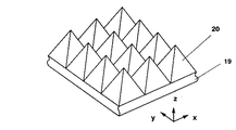
図2はプリズムアレイの斜視図である。各プリズム20は四角錐プリズムであり、対向するプリズム斜面の角度は90度である。プリズムアレイ19のピッチは、蛍光基板14への反射光の拡がりを小さくするため、20〜50μmとしている。プリズムアレイ19はガラスもしくは樹脂の成形により形成される。
FIG. 2 is a perspective view of the prism array. Each
図3は蛍光基板とプリズムアレイでの光線の様相を示した模式図である。図中には、蛍光発光する光の配光21とプリズム面で反射した光で拡散反射する光の配光22を示している。蛍光発光したランバーシアン分布の配光21は、プリズム面で屈折光と、全反射を含む反射光に分離され、その反射光は隣接するプリズム面でさらに反射し、蛍光基板14へ入射する。蛍光基板14の蛍光領域へ入射した光は、蛍光体層での拡散反射と反射膜面15での反射により、再び、ランバーシアン分布の配光22となり、再びプリズムアレイ19へ入射する。このような、蛍光基板14とプリズムアレイ19の間の多重反射により、プリズムアレイ19を出射する光の指向性が高くなり、立体角が小さい光束へ変換される。出射光束は完全拡散配光の場合と比べて、光の進行方向の光軸を0度として、±45度の範囲で略1.4倍向上する。
FIG. 3 is a schematic diagram showing the appearance of light rays on the fluorescent substrate and the prism array. In the figure, a
図4に、蛍光基板とプリズムアレイの構成を示す。同図(a)は、蛍光基板14とプリズムアレイ19の正面図、同図(b)は、プリズムアレイ19の平面図、同図(c)は、蛍光面17の平面図である。出射光側より、プリズムアレイ19および蛍光面17を観察したものである。25は照射されるレーザー光のスポット光を示している。蛍光面17は円環状の蛍光領域(斜線部)24と円環状の透過領域23を径方向に交互に形成したものである。透過領域23は透明基板を拡散面にしたものであり、その円環幅は、蛍光領域24の円環幅の略1/2である。蛍光面17へ入射するスポット光25は蛍光領域24と透過領域23とを照射するよう配置している。図4ではスポット光25の入射領域に対して、蛍光領域24と透過領域23の円環は各1本である。蛍光領域24と透過領域23の円環幅を狭く形成して、各2本以上の複数とすることで、スポット光25と蛍光および透過領域の位置ずれによる蛍光色光と透過青色光の強度変化を小さくすることもできる。プリズムアレイ19は蛍光面17の円環状の蛍光領域に対応してプリズムアレイ部(水平線部)を形成している。透過領域にはプリズムアレイは形成しない。透過領域23は表面を微細な凹凸形状とした拡散面であり、ピーク強度の1/2となる角度である拡散角が略5度の拡散面である。このため、透過領域を拡散透過する光の配光は指向性の高く、その光の立体角は小さい。拡散面とするのは、照射されるレーザー光のスペックルの緩和と、スポット光の強度分布を均一化するためである。プリズムアレイ19はスペーサーを用いて、蛍光面に微小な空気層を介して配置しているが、蛍光面やプリズムアレイと一定の屈折率差をもつ接着剤で貼合してもよい。貼合することにより、蛍光面とプリズム面との距離が狭くなり、スポット光を小さくすることができる。
FIG. 4 shows the configuration of the fluorescent substrate and the prism array. 2A is a front view of the
蛍光領域24の蛍光体層には青成分の光により励起され緑、赤成分を含んだ黄色を発光するCe付活YAG系黄色蛍光体を形成している。この蛍光体の結晶母体の代表的な化学組織はY3Al5O12である。スポット光で励起された蛍光領域24は緑、赤成分の光を発光し、透過領域23は青色光を出射する。蛍光基板17は回転させることにより、励起光による蛍光体の温度上昇を抑制し、蛍光変換効率を安定に維持することができる。また、プリズムアレイの温度上昇も抑制できる。蛍光体はYAG系黄色発光体と同様な発光特性をもつ酸化物蛍光体であるオルソシリケート系蛍光体を用いてもよい。
In the phosphor layer of the
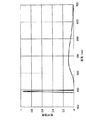
図5に、光源装置からの出射光の分光特性を示す。青成分はレーザーの発光、緑と赤の成分は蛍光発光の分光特性である。青成分と緑、赤成分の比率は、円環状の蛍光面の蛍光領域と透過領域の幅の比率と、それらの面の透過率により、制御可能であり、所望の白色色度を得ることができる。プリズムアレイを備えることにより、光源装置からの出射光束は完全拡散面の配光よりも±45度の範囲で略1.4倍向上できる。 FIG. 5 shows the spectral characteristics of the light emitted from the light source device. The blue component is the laser emission, and the green and red components are the fluorescence emission spectral characteristics. The ratio of the blue component to the green and red components can be controlled by the ratio of the width of the fluorescent region to the transmissive region of the annular phosphor screen and the transmittance of those surfaces, and the desired white chromaticity can be obtained. it can. By providing the prism array, the luminous flux emitted from the light source device can be improved by about 1.4 times in the range of ± 45 degrees from the light distribution on the complete diffusion surface.
以上のように、複数のレーザーと、蛍光領域と透過領域を形成した蛍光面と反射膜面とを備えた蛍光基板と、蛍光基板近傍に配置したプリズムアレイにより、長寿命で、エタンデユの小さい光を出射する光利用効率の高い光源装置が構成できる。この光源装置と、ライトバルブを用いて投写型表示装置を構成することにより、長寿命であり、高効率な投写型表示装置を構成することができる。 As described above, a long-life, low-eternity light is achieved by a plurality of lasers, a fluorescent substrate having a fluorescent surface and a reflective film surface on which a fluorescent region and a transmissive region are formed, and a prism array disposed in the vicinity of the fluorescent substrate. Thus, a light source device with high light utilization efficiency can be configured. By constructing a projection display device using this light source device and a light valve, it is possible to construct a projection display device having a long life and high efficiency.
(実施の形態2)
図6は、本発明の実施の形態を示す投写型表示装置の構成図である。
(Embodiment 2)
FIG. 6 is a configuration diagram of a projection display apparatus according to the embodiment of the present invention.
液晶ライトバルブとして、TNモードもしくはVAモードであって、画素領域に薄膜トランジスタを形成したアクティブマトリクス方式の透過型の液晶パネルを用いている。 As the liquid crystal light valve, a TN mode or VA mode transmissive liquid crystal panel of an active matrix type in which a thin film transistor is formed in a pixel region is used.
光源装置28は、青色の半導体レーザー11、レンズアレイ12、集光レンズ13、透明基板16上に反射膜面15と蛍光面17とを形成した蛍光基板14、モーター18、プリズムアレイ19で構成され、以上は本発明の光源装置である。29は集光レンズ、30、31はそれぞれ第一、第二のレンズアレイ板、32は偏光変換光学素子、33は重畳用レンズ、34は青反射のダイクロイックミラー、35は緑反射のダイクロイックミラー、36、37、38は反射ミラー、39、40はリレーレンズ、41、42、43はフィールドレンズ、44、45、46は入射側偏光板、47、48、49は液晶パネル、50、51、52は出射側偏光板、53は赤反射のダイクロイックミラーと青反射のダイクロイックミラーから構成される色合成プリズム、54は投写レンズである。
The
光源装置28の蛍光基板14とプリズムアレイ19は(図4)に示す蛍光基板とプリズムアレイを用いている。光源装置28から出射した白色光は、集光レンズ29より集光され、略平行光に変換される。略平行光に変換された光は、複数のレンズ素子から構成される第一のレンズアレイ板30に入射する。第一のレンズアレイ板30に入射した光束は多数の光束に分割される。分割された多数の光束は、複数のレンズから構成される第二のレンズアレイ板31に収束する。第一のレンズアレイ板30のレンズ素子は液晶パネルと相似形の開口形状である。第二のレンズアレイ板31のレンズ素子は第一のレンズアレイ板30と液晶パネル47、48、49とが略共役関係となるようにその焦点距離を決めている。第二のレンズアレイ板31から出射した光は偏光変換光学素子32に入射する。偏光変換光学素子32は、偏光分離プリズムと1/2波長板により構成され、光源からの自然光を一つの偏光方向の光に変換する。偏光変換光学素子32からの光は重畳用レンズ33に入射する。重畳用レンズ33は第二のレンズアレイ板31の各レンズ素子からの出射した光を液晶パネル47、48、49上に重畳照明するためのレンズである。集光レンズ29、第一および第二のレンズアレイ板30、31と、偏光変換光学素子32と、重畳用レンズ33が照明手段としている。重畳用レンズ33からの光は、色分離手段である青反射のダイクロイックミラー34、緑反射のダイクロイックミラー35により、青、緑、赤の色光に分離される。緑の色光はフィールドレンズ41、入射側偏光板44を透過して、液晶パネル47に入射する。青の色光は反射ミラー36で反射した後、フィールドレンズ42、入射側偏光板45を透過して液晶パネル48に入射する。赤の色光はリレーレンズ39、40や反射ミラー37、38を透過屈折および反射して、フィールドレンズ43、入射側偏光板46を透過して、液晶パネル49に入射する。
As the
3枚の液晶パネル47、48、49は映像信号に応じた画素への印加電圧の制御により入射する光の偏光状態を変化させ、それぞれの液晶パネル47、48、49の両側に透過軸を直交するように配置したそれぞれの入射側偏光板44、45、46および出射側偏光板50、51、52を組み合わせて光を変調し、緑、青、赤の画像を形成する。出射側偏光板50、51、52を透過した各色光は色合成プリズム53により、赤、青の各色光がそれぞれ赤反射のダイクロイックミラー、青反射のダイクロイックミラーによって反射し、緑の色光と合成され、投写レンズ54に入射する。投写レンズ54に入射した光は、スクリーン(図示せず)上に拡大投写される。光源装置28から出射する光の指向性が高く、エタンデユが小さい光であるため、投写型表示装置の光利用効率が高くなる。また、ライトバルブには、時分割方式ではなく偏光を利用する3枚の液晶パネルを用いているため、カラーブレイキングがなく色再現が良好で、明るく高精細な投写画像を得ることができる。
The three
液晶ライトバルブとして、透過型の液晶パネルを用いたが、反射型の液晶パネルを用いて構成してもよい。反射型の液晶パネルを用いることにより、小型で高精細な投写型表示装置が構成できる。 A transmissive liquid crystal panel is used as the liquid crystal light valve, but a reflective liquid crystal panel may be used. By using a reflective liquid crystal panel, a compact and high-definition projection display device can be configured.
以上のように、固体光源と、円環状に蛍光領域と透過領域を形成した蛍光面と反射膜面とを備えた蛍光基板と、蛍光基板近傍に配置したプリズムアレイで構成された光源装置を用いて投写型表示装置を構成することにより、エタンデユが小さい光源装置が構成でき、長寿命であって、高効率な投写型表示装置を構成することができる。 As described above, a light source device composed of a solid-state light source, a fluorescent substrate having a fluorescent surface and a reflective film surface in which a fluorescent region and a transmission region are formed in an annular shape, and a prism array disposed in the vicinity of the fluorescent substrate is used. By configuring the projection display device in this manner, a light source device with a small etendue can be configured, and a long-life and high-efficiency projection display device can be configured.
(実施の形態3)
図7は、本発明の実施の形態を示す投写型表示装置の構成図である。
(Embodiment 3)
FIG. 7 is a configuration diagram of a projection display apparatus showing an embodiment of the present invention.
ライトバルブとして、時分割方式の1つのDMDを用いている。光源装置78は、青色の半導体レーザー61、レンズアレイ62、集光レンズ63、透明基板66上に反射膜面65と蛍光面67とを形成した蛍光基板64、モーター68で構成され、以上は本発明の実施の形態1、2に示す光源装置と同様な構成である。蛍光基板64とプリズムアレイ69には構成が異なるものを用いている。80は集光レンズ、81はロッド、82はリレーレンズ、83は反射ミラー、84はフィールドレンズ、85は全反射プリズム、86はDMD、87は投写レンズである。光源装置78の蛍光基板64の蛍光面67には、回転方向に3分割した領域に緑、赤成分を蛍光する蛍光体層を形成した蛍光領域と透過領域を形成している。光源装置78から出射する光は、蛍光基板64の回転により、時系列的に緑、赤、青の色光を出射する。光源装置78からの光は、集光レンズ80により、ロッド81の入射面に集光する。ロッド81は入射面と出射面が矩形の柱状ガラスである。ロッド81に入射した光は、全反射を含む多重反射により、ロッド81の出射面まで伝播する。入射面では不均一な光束が出射面では均一な光束となる。ロッド81からの出射光は、リレーレンズ82、反射ミラー83、フィールドレンズ84、全反射プリズム85をそれぞれ屈折、反射後、DMD86に入射する。リレーレンズ82、フィールドレンズ84のそれぞれの面間隔と焦点距離は、ロッド81の出射面とDMD86面が共役な関係となるように決めている。フィールドレンズ84は照明光を効率よく投写レンズ87に集光する。全反射プリズム85は照明光を全反射し、DMD86からの投写光を透過するプリズムである。ロッド81からの出射光は、DMD86上に表示領域と相似な矩形照明となり、DMD86面を高効率で均一に照明する。集光レンズ80、ロッド81、リレーレンズ82、反射ミラー83、フィールドレンズ84、全反射プリズム85を照明手段としている。DMD86に入射する光は映像信号に応じて、画像形成に必要な光束のみを偏向し、全反射プリズム85を透過後、投写レンズ87に入射する。投写レンズ87はDMD86で変調形成される画像光を拡大投写する。ライトバルブに、1つのDMDを用いているため、小型軽量な投写型表示装置が構成できる。
As the light valve, one time-division DMD is used. The
図8に、蛍光基板とプリズムアレイの構成図を示す。同図(a)は、蛍光基板64とプリズムアレイ69の正面図、同図(b)は、プリズムアレイ69の平面図、同図(c)は、蛍光面67の平面図である。蛍光基板64は回転制御可能な円基板である。出射光側より、プリズムアレイ69および蛍光面67を観察したものである。73は照射されるレーザー光のスポット光を示している。蛍光面67は回転方向に、緑成分の蛍光領域(斜線部)70と赤成分の蛍光領域(垂直線部)71と透過領域72を分割形成したものである。透過領域72は透明基板を拡散面にしたものである。蛍光基板の回転により、蛍光面67へ入射するスポット光73は、時系列的に蛍光領域70、71と透過領域72を照射し、それぞれ緑、赤の色光を蛍光発光もしくは青の色光を拡散透過する。蛍光領域70、71と透過領域72の分割角度を変えることにより、時系列に出射する色光の比率を変え、所望のホワイトバランスの光を得ることができる。プリズムアレイ69は蛍光面67の蛍光領域に対応してプリズムアレイ領域(水平線部)を形成している。透過領域72にはプリズムアレイは形成しない。透過領域72は表面を微細な凹凸形状とした拡散面であり、ピーク強度の1/2となる角度である拡散角が略5度の拡散面である。このため、透過領域を拡散透過する光の配光は指向性の高く、プリズムアレイを形成する必要がない。拡散面とするのは、照射されるレーザー光のスペックルの緩和と、スポット光の強度分布を均一化するためである。プリズムアレイ69はスペーサーを用いて、蛍光面67と微小な空気層を介して配置しているが、蛍光面67やプリズムアレイ69と一定の屈折率差をもつ接着剤で貼合してもよい。接着貼合することにより、蛍光面67とプリズムアレイ69面との距離が狭くなり、スポット光を小さくすることができる。蛍光領域70の蛍光体層には青成分の光により励起され緑成分を含んだCe付活YAG系黄色蛍光体であり、その蛍光体には発光ピークが540nm付近で相対的に赤成分が少ない蛍光体を選択して用いている。蛍光領域71の蛍光体層には青成分の光より励起され、赤成分を含んだ成分を蛍光する窒化物蛍光体を形成している。窒化物蛍光体としてはCa2Si5N8:Euがある。この蛍光体は波長610nm近傍に発光ピークがあり半値幅100nm程度で広帯域に発光する。また、温度上昇による変換効率低下もYAG系黄色蛍光体よりも小さい。励起された蛍光領域70、71は緑、赤成分の光を蛍光発光し、透過領域72は青色光を出射する。蛍光基板64は回転させることにより、励起光による蛍光体の温度上昇を抑制し、蛍光変換効率を安定に維持することができる。
FIG. 8 shows a configuration diagram of the fluorescent substrate and the prism array. 2A is a front view of the
緑色用の蛍光体はYAG系黄色発光体と同様な発光特性をもつ酸化物蛍光体であるオルソシリケート系蛍光体を用いてもよい。赤色用の蛍光体は酸窒化物蛍光体を用いてもよい。酸窒化物蛍光体としてはCaAlSiN3:Eu蛍光体がある。この蛍光体は650nm付近に発光ピークがあり半値幅100nm程度で広帯域に発光する。 The green phosphor may be an orthosilicate phosphor that is an oxide phosphor having the same emission characteristics as the YAG yellow phosphor. An oxynitride phosphor may be used as the red phosphor. As the oxynitride phosphor, there is a CaAlSiN 3 : Eu phosphor. This phosphor has an emission peak in the vicinity of 650 nm, and emits light in a wide band with a half-value width of about 100 nm.
以上のように、固体光源と、回転方向に分割した領域にそれぞれ緑、赤成分を蛍光発光する蛍光領域と透過領域を形成した蛍光面と反射膜面とを備えた蛍光基板と、蛍光基板近傍に配置したプリズムアレイで構成された光源装置を用いて投写型表示装置を構成することにより、エタンデユが小さい光源が構成でき、長寿命であって、高効率な投写型表示装置を構成することができる。 As described above, a solid-state light source, a fluorescent substrate including a fluorescent region that fluoresces green and red components in a region divided in the rotation direction, a fluorescent surface that forms a transmission region, and a reflective film surface, and the vicinity of the fluorescent substrate By constructing a projection display device using a light source device composed of a prism array arranged in a light source, a light source with a small etendue can be constructed, and a long-life and high-efficiency projection display device can be constructed. it can.
なお、前記いずれの実施の形態においても、光源装置のレーザーを複数備えているが、レーザー光の強度が大きければ、レーザーを複数備える必要はなく、また、集光手段も省略することができる。 In any of the above embodiments, a plurality of lasers of the light source device are provided. However, if the intensity of the laser beam is high, it is not necessary to provide a plurality of lasers, and the light condensing means can be omitted.
本発明は、ライトバルブを用いた投写型表示装置に関するものである。 The present invention relates to a projection display device using a light valve.
11、61 半導体レーザー
12、62 レンズアレイ
13、63 集光レンズ
14、64 蛍光基板
15、65 反射膜面
16、66 透明基板
17、67 蛍光面
18、68 モーター
19、69 プリズムアレイ
20 プリズム
21、22 配光
23、72 透過領域
24 蛍光領域
25、73 スポット光
28、78 光源装置
29、80 集光レンズ
30 第一のレンズアレイ板
31 第二のレンズアレイ板
32 偏光変換光学素子
33 重畳用レンズ
34 青反射のダイクロイックミラー
35 緑反射のダイクロイックミラー
36、37、38、83 反射ミラー
39、40、82 リレーレンズ
41、42、43、84 フィールドレンズ
44、45、46 入射側偏光板
47、48、49 液晶パネル
50、51、52 出射側偏光板
53 色合成プリズム
54、87 投写レンズ
70 緑成分の蛍光領域
71 赤成分の蛍光領域
81 ロッド
85 全反射プリズム
86 DMD
DESCRIPTION OF
Claims (3)
前記レーザーからの光を受けて蛍光を発する蛍光体層を有する円環状の蛍光領域と前記レーザーからの光を透過する円環状の透過領域とを径方向に交互に形成した蛍光基板と、
前記蛍光が前記蛍光基板から出射する側で前記蛍光領域に対応し且つ前記透過領域に対応しないところに設けられ、入射した光の入射角に応じて屈折光と反射光とに分離するプリズム面を有するプリズムアレイと、を備える光源装置であって、
前記プリズムアレイは、前記プリズム面と前記蛍光基板との間の多重反射により、前記蛍光の指向性を高めることを特徴とする光源装置。 With laser,
A fluorescent substrate in which an annular fluorescent region having a phosphor layer that emits fluorescence upon receiving light from the laser and an annular transmission region that transmits light from the laser are alternately formed in the radial direction ;
A prism surface is provided on the side where the fluorescent light exits from the fluorescent substrate , corresponding to the fluorescent region and not corresponding to the transmissive region, and is separated into refracted light and reflected light according to an incident angle of incident light. A prism array, and a light source device comprising:
The light source device characterized in that the prism array enhances the directivity of the fluorescence by multiple reflection between the prism surface and the fluorescent substrate.
前記プリズムアレイは、
複数の四角錐プリズムを有しており、
前記蛍光基板と対向する入射面側が四角錐の底面となるよう、前記複数の四角錐プリズムが配置されることを特徴とする光源装置。 The light source device according to claim 1,
The prism array is
Having a plurality of square pyramid prisms,
The light source device, wherein the plurality of quadrangular pyramid prisms are arranged such that an incident surface side facing the fluorescent substrate is a bottom surface of the quadrangular pyramid.
前記光源部に請求項1または2記載の光源装置を用いることを特徴とする投写型表示装置。 A light source unit, an image forming unit that forms an image in response to a video signal, an illumination unit that collects light from the light source device to illuminate the image forming unit, and an image formed by the image forming unit. A projection display device comprising: a projection unit that performs enlargement projection;
3. A projection display device using the light source device according to claim 1 or 2 for the light source unit.
Priority Applications (1)
| Application Number | Priority Date | Filing Date | Title |
|---|---|---|---|
| JP2010162499A JP5605047B2 (en) | 2010-07-20 | 2010-07-20 | Light source device and projection display device using the same |
Applications Claiming Priority (1)
| Application Number | Priority Date | Filing Date | Title |
|---|---|---|---|
| JP2010162499A JP5605047B2 (en) | 2010-07-20 | 2010-07-20 | Light source device and projection display device using the same |
Publications (3)
| Publication Number | Publication Date |
|---|---|
| JP2012027052A JP2012027052A (en) | 2012-02-09 |
| JP2012027052A5 JP2012027052A5 (en) | 2013-06-27 |
| JP5605047B2 true JP5605047B2 (en) | 2014-10-15 |
Family
ID=45780089
Family Applications (1)
| Application Number | Title | Priority Date | Filing Date |
|---|---|---|---|
| JP2010162499A Active JP5605047B2 (en) | 2010-07-20 | 2010-07-20 | Light source device and projection display device using the same |
Country Status (1)
| Country | Link |
|---|---|
| JP (1) | JP5605047B2 (en) |
Families Citing this family (21)
| Publication number | Priority date | Publication date | Assignee | Title |
|---|---|---|---|---|
| JP6007533B2 (en) * | 2012-03-21 | 2016-10-12 | カシオ計算機株式会社 | Light source device and projector device |
| JP5919476B2 (en) * | 2012-05-10 | 2016-05-18 | パナソニックIpマネジメント株式会社 | Light source device and video display device |
| JP6270012B2 (en) * | 2012-09-20 | 2018-01-31 | カシオ計算機株式会社 | Light source device, lighting method of light source device, and projector |
| JP6086193B2 (en) * | 2012-09-20 | 2017-03-01 | カシオ計算機株式会社 | Light source device, lighting method of light source device, and projector |
| CN105159020B (en) * | 2012-10-31 | 2017-07-11 | 深圳市绎立锐光科技开发有限公司 | Light-source system and relevant projecting system |
| JP6094866B2 (en) * | 2013-01-15 | 2017-03-15 | Zero Lab株式会社 | Illumination optics |
| JP5928383B2 (en) | 2013-03-22 | 2016-06-01 | ソニー株式会社 | Light source device and display device |
| TWI493275B (en) * | 2013-04-20 | 2015-07-21 | Appotronics China Corp | A lighting device and a projection system |
| US9863759B2 (en) | 2014-10-17 | 2018-01-09 | Ricoh Company, Ltd. | Illumination apparatus, pattern irradiation device, and system |
| JP6428193B2 (en) | 2014-11-21 | 2018-11-28 | 日亜化学工業株式会社 | Wavelength conversion member and projector provided with the wavelength conversion member |
| WO2016121721A1 (en) * | 2015-01-28 | 2016-08-04 | コニカミノルタ株式会社 | Wavelength conversion member, and image formation device |
| JP6503766B2 (en) * | 2015-02-02 | 2019-04-24 | セイコーエプソン株式会社 | Lighting device and projector |
| JP6464781B2 (en) * | 2015-02-02 | 2019-02-06 | セイコーエプソン株式会社 | Lighting device and projector |
| WO2016181858A1 (en) * | 2015-05-08 | 2016-11-17 | コニカミノルタ株式会社 | Light source device and projection device |
| JP6748905B2 (en) * | 2015-08-20 | 2020-09-02 | パナソニックIpマネジメント株式会社 | Light emitting device |
| JP2018169413A (en) * | 2015-08-28 | 2018-11-01 | パナソニックIpマネジメント株式会社 | Lighting device and lighting system |
| JP6354725B2 (en) * | 2015-10-06 | 2018-07-11 | ウシオ電機株式会社 | Fluorescent light source device |
| JP2018084757A (en) * | 2016-11-25 | 2018-05-31 | セイコーエプソン株式会社 | Illumination apparatus and projector |
| JP6977285B2 (en) | 2017-03-28 | 2021-12-08 | セイコーエプソン株式会社 | Wavelength converters, light source devices and projectors |
| US20230040423A1 (en) * | 2020-01-22 | 2023-02-09 | Sony Group Corporation | Optical element, light source device, and projector |
| CN113623611B (en) * | 2021-07-19 | 2023-06-02 | 山西汉威激光科技股份有限公司 | Intelligent headlight light source light path structure for projection of automobile tail |
Family Cites Families (5)
| Publication number | Priority date | Publication date | Assignee | Title |
|---|---|---|---|---|
| JP2003330111A (en) * | 2002-05-10 | 2003-11-19 | Olympus Optical Co Ltd | Light emitting unit, illuminator, and projection display device |
| JP2004191718A (en) * | 2002-12-12 | 2004-07-08 | Mitsubishi Electric Corp | Led light source device |
| JP4829470B2 (en) * | 2003-05-14 | 2011-12-07 | Necディスプレイソリューションズ株式会社 | Projection display |
| JP2006332638A (en) * | 2005-04-28 | 2006-12-07 | Toyoda Gosei Co Ltd | Light emitting diode apparatus |
| JP5527571B2 (en) * | 2008-09-30 | 2014-06-18 | カシオ計算機株式会社 | Light emitting device, light source device, and projector using the light source device |
-
2010
- 2010-07-20 JP JP2010162499A patent/JP5605047B2/en active Active
Also Published As
| Publication number | Publication date |
|---|---|
| JP2012027052A (en) | 2012-02-09 |
Similar Documents
| Publication | Publication Date | Title |
|---|---|---|
| JP5605047B2 (en) | Light source device and projection display device using the same | |
| JP6056001B2 (en) | Light source device and projection display device | |
| JP5906416B2 (en) | Illumination device and projection display device | |
| JP5914878B2 (en) | Light source device and projection display device | |
| US9488902B2 (en) | Illuminator and projector | |
| USRE48753E1 (en) | Projection image display device including optical system | |
| JP5895226B2 (en) | Light source device and projection display device | |
| JP6090875B2 (en) | Illumination optical system and projector | |
| JP5445379B2 (en) | projector | |
| US9645481B2 (en) | Light source apparatus and projection display apparatus | |
| JP2024023800A (en) | Light source device, image projection device, and light source optical system | |
| JP2012008303A (en) | Light source device and projection type display device using the same | |
| US11181814B2 (en) | Light source device and projector | |
| JP2013178290A (en) | Light source device and illuminating device | |
| JP2012118302A (en) | Light source device and projector | |
| WO2015111145A1 (en) | Light source device and image display device using same | |
| JP2018084757A (en) | Illumination apparatus and projector | |
| US20200033707A1 (en) | Light source device and projector | |
| US11523093B2 (en) | Light source apparatus and projector | |
| JP2020177070A (en) | Light source device and projection type display unit | |
| JP2017083907A (en) | Projector and method for irradiating image forming element with illumination light | |
| JP5804536B2 (en) | Illumination optical system and projection display device | |
| WO2021186612A1 (en) | Light source device and projector | |
| JP7108901B2 (en) | Lighting device and projection display device | |
| JP2022017670A (en) | Light source device and projection-type display device |
Legal Events
| Date | Code | Title | Description |
|---|---|---|---|
| A521 | Written amendment |
Free format text: JAPANESE INTERMEDIATE CODE: A523 Effective date: 20130513 |
|
| A621 | Written request for application examination |
Free format text: JAPANESE INTERMEDIATE CODE: A621 Effective date: 20130513 |
|
| RD01 | Notification of change of attorney |
Free format text: JAPANESE INTERMEDIATE CODE: A7421 Effective date: 20130612 |
|
| A977 | Report on retrieval |
Free format text: JAPANESE INTERMEDIATE CODE: A971007 Effective date: 20131122 |
|
| A131 | Notification of reasons for refusal |
Free format text: JAPANESE INTERMEDIATE CODE: A131 Effective date: 20131217 |
|
| RD01 | Notification of change of attorney |
Free format text: JAPANESE INTERMEDIATE CODE: A7421 Effective date: 20140107 |
|
| A521 | Written amendment |
Free format text: JAPANESE INTERMEDIATE CODE: A523 Effective date: 20140205 |
|
| RD01 | Notification of change of attorney |
Free format text: JAPANESE INTERMEDIATE CODE: A7421 Effective date: 20140417 |
|
| TRDD | Decision of grant or rejection written | ||
| A01 | Written decision to grant a patent or to grant a registration (utility model) |
Free format text: JAPANESE INTERMEDIATE CODE: A01 Effective date: 20140729 |
|
| A61 | First payment of annual fees (during grant procedure) |
Free format text: JAPANESE INTERMEDIATE CODE: A61 Effective date: 20140811 |
|
| R151 | Written notification of patent or utility model registration |
Ref document number: 5605047 Country of ref document: JP Free format text: JAPANESE INTERMEDIATE CODE: R151 |