JP5598043B2 - 90-degree optical hybrid interferometer and manufacturing method of 90-degree optical hybrid interferometer - Google Patents
90-degree optical hybrid interferometer and manufacturing method of 90-degree optical hybrid interferometer Download PDFInfo
- Publication number
- JP5598043B2 JP5598043B2 JP2010064473A JP2010064473A JP5598043B2 JP 5598043 B2 JP5598043 B2 JP 5598043B2 JP 2010064473 A JP2010064473 A JP 2010064473A JP 2010064473 A JP2010064473 A JP 2010064473A JP 5598043 B2 JP5598043 B2 JP 5598043B2
- Authority
- JP
- Japan
- Prior art keywords
- optical
- phase
- optical signal
- signal
- local oscillation
- Prior art date
- Legal status (The legal status is an assumption and is not a legal conclusion. Google has not performed a legal analysis and makes no representation as to the accuracy of the status listed.)
- Active
Links
Images


Classifications
-
- G—PHYSICS
- G02—OPTICS
- G02B—OPTICAL ELEMENTS, SYSTEMS OR APPARATUS
- G02B6/00—Light guides; Structural details of arrangements comprising light guides and other optical elements, e.g. couplings
- G02B6/10—Light guides; Structural details of arrangements comprising light guides and other optical elements, e.g. couplings of the optical waveguide type
- G02B6/12—Light guides; Structural details of arrangements comprising light guides and other optical elements, e.g. couplings of the optical waveguide type of the integrated circuit kind
- G02B6/122—Basic optical elements, e.g. light-guiding paths
- G02B6/125—Bends, branchings or intersections
-
- H—ELECTRICITY
- H04—ELECTRIC COMMUNICATION TECHNIQUE
- H04B—TRANSMISSION
- H04B10/00—Transmission systems employing electromagnetic waves other than radio-waves, e.g. infrared, visible or ultraviolet light, or employing corpuscular radiation, e.g. quantum communication
- H04B10/60—Receivers
- H04B10/61—Coherent receivers
-
- Y—GENERAL TAGGING OF NEW TECHNOLOGICAL DEVELOPMENTS; GENERAL TAGGING OF CROSS-SECTIONAL TECHNOLOGIES SPANNING OVER SEVERAL SECTIONS OF THE IPC; TECHNICAL SUBJECTS COVERED BY FORMER USPC CROSS-REFERENCE ART COLLECTIONS [XRACs] AND DIGESTS
- Y10—TECHNICAL SUBJECTS COVERED BY FORMER USPC
- Y10T—TECHNICAL SUBJECTS COVERED BY FORMER US CLASSIFICATION
- Y10T156/00—Adhesive bonding and miscellaneous chemical manufacture
- Y10T156/10—Methods of surface bonding and/or assembly therefor
Description
本発明は90度光ハイブリッド干渉計に関し、特に光導波路技術を用いた平面光波回路で構成した90度光ハイブリッド干渉計に関する。 The present invention relates to a 90-degree optical hybrid interferometer, and more particularly to a 90-degree optical hybrid interferometer configured with a planar lightwave circuit using optical waveguide technology.
近年、100Gbit/秒を超える超高速通信において、波長利用効率、受信特性、分散補償能力に優れる偏波直交多重多値デジタル信号変調方式(DP−QPSK: Dual Polarization Differential Quadrature Phase Shift Keying)による通信技術が注目されている。DP−QPSK方式における受信器(レシーバ)には、光信号を偏波分離する機能と、偏波分離した光信号から位相情報を取り出すための90度光ハイブリッド機能が必要とされる。この位相情報は、互いにπの位相差を有するIpとIn、並びにIpとInに対してそれぞれπ/2の位相遅延を有する QpとQnとからなる、I−Q平面上の4値の位相情報である。 In recent years, in ultra-high-speed communication exceeding 100 Gbit / s, a communication technique based on a polarization orthogonal multiplex multi-phase digital signal modulation method (DP-QPSK: Dual Polarization Differential Shift Keying) excellent in wavelength utilization efficiency, reception characteristics, and dispersion compensation capability Is attracting attention. A receiver (receiver) in the DP-QPSK system is required to have a function of polarization-demultiplexing an optical signal and a 90-degree optical hybrid function for extracting phase information from the polarization-separated optical signal. This phase information is quaternary phase information on the IQ plane consisting of Ip and In having a phase difference of π, and Qp and Qn having a phase delay of π / 2 with respect to Ip and In, respectively. It is.
このような機能を有するレシーバは、高速データ通信を推進する業界団体であるOIF(Optical Internetworking Forum)で標準化が進められている。例えば8つの出力信号を出力するポートの配列順などはOIFにてその仕様が取り決められており、レシーバの開発はこれらのOIFの仕様に則って行われている。 The receiver having such a function is being standardized by OIF (Optical Internetworking Forum) which is an industry group promoting high-speed data communication. For example, the arrangement order of the ports that output eight output signals is determined by the OIF, and the development of the receiver is performed in accordance with these OIF specifications.
ところで、このようなDP−QPSK方式のレシーバの機能を実現するデバイスには、光導波路技術を用いた平面光波回路が有力とされている。光導波路技術は、半導体集積回路製造プロセスと同様の微細加工技術により、基板上に多様な形状の光導波路を形成するもので、集積化や量産に適したものである。 By the way, a planar lightwave circuit using an optical waveguide technique is considered to be a promising device for realizing the DP-QPSK receiver function. In the optical waveguide technology, optical waveguides having various shapes are formed on a substrate by the same microfabrication technology as in the semiconductor integrated circuit manufacturing process, which is suitable for integration and mass production.
このような光波回路によるDP−QPSK方式のレシーバは、近年開発が進められており、例えば非特許文献1には図6に示す光波回路構造が記載されている。図6の光波回路は、上述した偏波分離機能と90度光ハイブリッド機能とを平面光回路内に集積したものであり、このうち90度光ハイブリッド機能を担っている部分の平面光回路の構成を模式図として図7に示す。 DP-QPSK receivers using such lightwave circuits have been developed in recent years. For example, Non-Patent Document 1 describes a lightwave circuit structure shown in FIG. The lightwave circuit of FIG. 6 is obtained by integrating the above-described polarization separation function and 90-degree optical hybrid function in a planar optical circuit, and among these, the configuration of the planar optical circuit of the portion carrying the 90-degree optical hybrid function Is schematically shown in FIG.
この光回路においてTE(Transverse Electric)光信号およびTM(Transverse Magnetic)光信号について90度光ハイブリッド機能は、それぞれ4つのアームが干渉計を構成する。そして、当該4本のアームの内、特定のアームを他のアームより光導波路内を伝播する信号光波長の1/4に相当する分だけ長くすることにより光路長差を付与して実現される。非特許文献1に記載の90度光ハイブリッド干渉計では、アーム33とアーム35の2つが、それぞれ他のアームより光路長差分だけ長い。このように光路長差を付与すると、出力される干渉信号は図8に示すように、TE光信号およびTM光信号について、それぞれπ/2の位相差を有する4つの光信号として出力される。図8において横軸はTE信号光と局発光の位相差を表しており、InTEとQnTE、並びにIpTEとQpTEは、共にπ/2の位相差を持って出力される。またInTEとIpTE、並びにQnTEとQpTEは、共にπの位相差を持って出力される。同様に、InTMとQnTM、並びにIpTMとQpTMは、共にπ/2の位相差を持って出力される。またInTMとIpTM、並びにQnTMとQpTMは、共にπの位相差を持って出力される。なお、図7におけるこれらの出力信号が出力されるポートの配列は、OIFで取り決められた仕様に従ったものになっている。
In this optical circuit, the 90-degree optical hybrid function for the TE (Transverse Electric) optical signal and the TM (Transverse Magnetic) optical signal has four arms each constituting an interferometer. Then, a specific arm of the four arms is made longer than the other arm by an amount corresponding to ¼ of the signal light wavelength propagating in the optical waveguide, thereby realizing an optical path length difference. . In the 90-degree optical hybrid interferometer described in Non-Patent Document 1, the two
しかしながら、出力ポートを上記のOIF標準に則って配置する場合、図7のような光回路構成では、2分岐した局部発振光を伝播する光導波路のうち一方が、信号光を伝播する光導波路と交差するポイントが生じる。この交差部においては、クロストーク、すなわち本来導波してはならない導波路側に光が結合してしまう現象の防止はもちろん、過剰損の発生を回避するために、交差角度をできるだけ直角に近づけた設計としなければならい。また、90度光ハイブリッド干渉計では、スキュー特性を満足させるため入力から出力までの各光パスにおいて光路長が同一であることが望ましい。すなわち、このような構成においては交差角度と光路長の制約を受けることになり、交差部数が多いほど光導波路のレイアウトが冗長化・複雑化するため、OIF標準の出力ポート配置を実現するための設計自由度を損なうだけでなく、チップサイズも大きくなる。 However, when the output port is arranged in accordance with the above-mentioned OIF standard, in the optical circuit configuration as shown in FIG. 7, one of the optical waveguides propagating the local oscillation light branched into two is an optical waveguide propagating the signal light. Intersect points occur. At this intersection, in order to prevent crosstalk, that is, the phenomenon that light is coupled to the waveguide side that should not be guided, the intersection angle should be as close to a right angle as possible to avoid excessive loss. Must be designed. In the 90-degree optical hybrid interferometer, it is desirable that the optical path length is the same in each optical path from input to output in order to satisfy the skew characteristics. That is, in such a configuration, the crossing angle and the optical path length are restricted, and the layout of the optical waveguide becomes redundant and complicated as the number of crossing portions increases, so that an OIF standard output port arrangement can be realized. Not only does the design freedom be lost, but the chip size also increases.
本発明の目的は、上記の問題点を解決し、OIF標準の出力ポート配置を実現しつつ、光導波路アームの交差部分を削減した光回路構成の、90度光ハイブリッド干渉計を提供することである。 An object of the present invention is to provide a 90-degree optical hybrid interferometer having an optical circuit configuration that solves the above-described problems and realizes an OIF standard output port arrangement while reducing the number of intersections of optical waveguide arms. is there.
本発明の90度光ハイブリッド干渉計は、偏波分離したTransverse Electric(TE)光信号およびTransverse Magnetic(TM)光信号から、それぞれ、互いにπの位相差を有する位相情報IpとIn、並びに前記Ipと前記Inに対してそれぞれπ/2の位相遅延を有する位相情報QpとQnとからなる、IQ平面上の4値の位相情報を取り出すための90度光ハイブリッド干渉計であって、前記偏波分離したTE光信号およびTM光信号をそれぞれ入力する2つの信号光入力ポートと、前記2つの信号光入力ポートの間に配置された、局部発振光を入力する局部発振光入力ポートと、前記信号光入力ポートから入力され、それぞれI相側とQ相側とに2分岐された、前記TE光信号およびTM光信号を伝播する信号光導波路アームと、前記局部発振光入力ポートから入力され、前記TE光信号側と前記TM光信号側とに2分岐された後、さらにそれぞれ2つに分岐された前記局部発振光を伝播する局部発振光導波路アームと、前記TE光信号側においてI相側とQ相側とに2分岐した前記TE光信号と、前記TE光信号側において2つに分岐された前記局部発振光とを、それぞれ一対ずつ結合する2つの光結合器と、前記TM光信号側においてI相側とQ相側とに2分岐した前記TM光信号と、前記TM光信号側において2つに分岐された前記局部発振光とを、それぞれ一対ずつ結合する2つの光結合器と、前記TE光信号側およびTM光信号側のそれぞれにおいて、2つの前記光結合器から出力される、対をなす信号光と局部発振光との位相差による4つの干渉信号を、それぞれ前記位相情報Ip、In、Qp、Qnとして取り出す4つの出力ポートと、を有し、前記TE光信号側および前記TM光信号側のそれぞれにおいて、前記I相側と前記Q相側のいずれか一方の、前記信号光導波路アームと前記局部発振光導波路アームとの対に、光路長差を設けることにより、前記I相側と前記Q相側の出力干渉信号IpとQp、並びにInとQnとの間にそれぞれ前記光路長差に対応する遅延位相差を与え、前記TE光信号側および前記TM光信号側のそれぞれにおいて、前記I相側の光結合器と前記Q相側の光結合器とがそれぞれ有する出力干渉特性同士の位相差と、前記遅延位相差とを、両者の合計で生じる、出力干渉信号Ipに対するQpの出力位相差、並びに出力干渉信号Inに対するQnの出力位相差が、共に+π/2となるように設定することにより、8つの前記出力ポートの出力信号を、上から前記TE光信号側のIp、In、Qp、Qn、および前記TM光信号側のIp、In、Qp、Qnの順に配列したことを特徴としている。
90-degree optical hybrid interferometer of the present invention, the Transverse Electric (TE) optical signal and Transverse Magnetic (T M) optical signal polarization splitting, respectively, phase information Ip and In have a phase difference of π from each other, and the A 90-degree optical hybrid interferometer for extracting quaternary phase information on an IQ plane, comprising phase information Qp and Qn having a phase delay of π / 2 with respect to Ip and In, respectively, Two signal light input ports for inputting the separated TE optical signal and TM optical signal, a local oscillation light input port for inputting local oscillation light, disposed between the two signal light input ports, The TE optical signal and the TM optical signal, which are input from the signal light input port and bifurcated into the I-phase side and the Q-phase side, respectively. Signal optical waveguide arm that propagates through the local oscillation light and the local oscillation light input port. The local oscillation light is branched into two after being branched into the TE optical signal side and the TM optical signal side, respectively. and the local oscillation light waveguide arms propagating said and TE
また本発明の90度光ハイブリッド干渉計の製造方法は、偏波分離したTransverse Electric(TE)光信号およびTransverse Magnetic(TM)光信号から、それぞれ、互いにπの位相差を有する位相情報IpとIn、並びに前記Ipと前記Inに対してそれぞれπ/2の位相遅延を有する位相情報QpとQnとからなる、I−Q平面上の4値の位相情報を取り出すための90度光ハイブリッド干渉計の製造方法であって、前記偏波分離したTE光信号およびTM光信号をそれぞれ入力する2つの信号光入力ポートと、前記2つの信号光入力ポートの間に配置された、局部発振光を入力する局部発振光入力ポートと、前記信号光入力ポートから入力され、それぞれI相側とQ相側とに2分岐された、前記TE光信号およびTM光信号を伝播する信号光導波路アームと、前記局部発振光入力ポートから入力され、前記TE光信号側と前記TM光信号側とに2分岐された後、さらにそれぞれ2つに分岐された前記局部発振光を伝播する局部発振光導波路アームと、前記TE光信号側においてI相側とQ相側とに2分岐した前記TE光信号と、前記TE光信号側において2つに分岐された前記局部発振光とを、それぞれ一対ずつ結合する2つの光結合器と、前記TM光信号側においてI相側とQ相側とに2分岐した前記TM光信号と、前記TM光信号側において2つに分岐された前記局部発振光とを、それぞれ一対ずつ結合する2つの光結合器と、前記TE光信号側およびTM光信号側のそれぞれにおいて、2つの前記光結合器から出力される、対をなす信号光と局部発振光との位相差による4つの干渉信号を、それぞれ前記位相情報Ip、In、Qp、Qnとして取り出す4つの出力ポートと、を構成し、前記TE光信号側および前記TM光信号側のそれぞれにおいて、前記I相側と前記Q相側のいずれか一方の、前記信号光導波路アームと前記局部発振光導波路アームとの対に、光路長差を設けることにより、前記I相側と前記Q相側の出力干渉信号IpとQp、並びにInとQnとの間にそれぞれ前記光路長差に対応する遅延位相差を与え、前記TE光信号側および前記TM光信号側のそれぞれにおいて、前記I相側の光結合器と前記Q相側の光結合器とがそれぞれ有する出力干渉特性同士の位相差と、前記遅延位相差とを、両者の合計で生じる、出力干渉信号Ipに対するQpの出力位相差、並びに出力干渉信号Inに対するQnの出力位相差が、共に+π/2となるように設定することにより、8つの前記出力ポートの出力信号を、上から前記TE光信号側のIp、In、Qp、Qn、および前記TM光信号側のIp、In、Qp、Qnの順に配列することを特徴としている。
The method of manufacturing the 90-degree optical hybrid interferometer according to the present invention includes a phase information Ip having a phase difference of π from each of a polarization-separated Transverse Electric (TE) optical signal and a Transverse Magnetic (T M ) optical signal. 90 degree optical hybrid interferometer for extracting quaternary phase information on the IQ plane, comprising In and phase information Qp and Qn each having a phase delay of π / 2 with respect to Ip and In The two methods of manufacturing a signal light input port for inputting the polarization-separated TE optical signal and the TM optical signal, and the local oscillation light arranged between the two signal light input ports are input. The local oscillation light input port to be input and the signal light input port, which are bifurcated into the I-phase side and the Q-phase side, respectively, A signal optical waveguide arm for propagating a TE optical signal and a TM optical signal, and a signal input from the local oscillation light input port, branched into two on the TE optical signal side and the TM optical signal side, and then further divided into two and the local oscillation light waveguide arms propagating branched the local oscillator light, wherein the TE
本発明によれば、OIF標準の出力ポート配置を実現しつつ、光導波路アームの交差部分を削減した光回路構成の、90度光ハイブリッド干渉計を提供することができる。 According to the present invention, it is possible to provide a 90-degree optical hybrid interferometer having an optical circuit configuration in which the intersections of the optical waveguide arms are reduced while realizing the OIF standard output port arrangement.
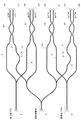
(第1の実施の形態)
図1は本発明の一実施の形態の90度光ハイブリッド干渉計の光導波路構成を示す模式図である。図1において1、2は偏波分離したTEおよびTM光信号をそれぞれ入力する信号光入力ポートである。3〜6は、それぞれ2つに分岐したTEおよびTM光信号を伝播する信号光導波路アームである。7は局部発振光を入力する局部発振光入力ポートで、信号光入力ポート1、2の間に配置されている。8〜11は、TE光信号側とTM光信号側とに2分岐した後、さらにそれぞれ2つに分岐した局部発振光を伝播する局部発振光導波路アームである。12〜15は信号光導波路アーム3〜6と局部発振光導波路アーム8〜11とをそれぞれ一対ずつ結合する光結合器である。16〜23は各光結合器から出力される、信号光と局部発振光との位相差による干渉信号を、I−Q平面上の4値の位相情報Ip、In、Qp、Qnとして取り出す出力ポートである。出力ポート16〜23より出力する干渉信号の配列は、上からIpTE、InTE、QpTE、QnTE、IpTM、InTM、QpTM、QnTM、の順で並んでいる。
(First embodiment)
FIG. 1 is a schematic diagram showing an optical waveguide configuration of a 90-degree optical hybrid interferometer according to an embodiment of the present invention. In FIG. 1,
TE光信号側およびTM光信号側のそれぞれにおいては、I相側とQ相側のいずれか一方の、信号光導波路アームと局部発振光導波路アームとの対が、光路長差を有した構造としている。すなわちI相側では3と8または4と9とのいずれか、Q相側では5と10または6と11とのいずれかのアーム対に、光路長差が設けられている。この光路長差は、対を構成するアームの一方の長さを光路長差分長くすることによって付与し、これによって当該光路長差分長くしたアーム内を伝播する光波は、その他のアーム内を伝播する光波よりも、各光結合器に入力する時点で位相遅延が生じる。その結果、各光結合器から出力する干渉信号に関しては、TE光信号側においては、IpTEとQpTE、並びにInTEとQnTEは、共に上記の光路長差に対応する位相差を持った関係となる。同様にTM光信号側においても、IpTMとQpTM、並びにInTMとQnTMは、やはり共に上記の光路長差に対応する位相差を持つ。
In each of the TE optical signal side and the TM optical signal side, the pair of the signal optical waveguide arm and the local oscillation optical waveguide arm on either the I-phase side or the Q-phase side has an optical path length difference. Yes. That is, an optical path length difference is provided for any of the
一方、光結合器はその構造によって出力干渉特性が異なり、同じ位相で入力された光信号でも各光結合器の出力干渉特性同士の差によって、出力する干渉信号に位相差が生じる。ここでは光結合器12と13との出力干渉特性の差によって生じる位相差分と、上記の光路長差に対応する位相差との合計で生じる、IpTEに対するQpTEの位相差、並びにInTEに対するQnTEの位相差を、共に+π/2となるように設定している。同様に、光結合器14と15との出力干渉特性の差によって生じる位相差分と、上記の光路長差に対応する位相差とを合計した、IpTMに対するQpTMの位相差、並びにInTMに対するQnTMの位相差を、共に+π/2となるように設定している。
On the other hand, optical couplers have different output interference characteristics depending on their structures. Even if optical signals are input in the same phase, a phase difference occurs in the output interference signals due to the difference between the output interference characteristics of each optical coupler. Here, the phase difference of QpTE with respect to IpTE and the level of QnTE with respect to InTE, which are the sum of the phase difference caused by the difference in output interference characteristics between
図1では、局部発振光導波路アーム8と9との間に、伝播する局部発振光のπ/2の位相差に相当する光路長差を設けている。すなわち、アーム9はアーム8に比べて光導波路内を伝播する局部発振光の波長の1/4の長さだけ長くしている。同様に局部発振光導波路アーム10と11との間も、伝播する局部発振光のπ/2の位相差に相当する光路長差を設けている。すなわち、アーム11はアーム10に比べて光導波路内を伝播する局部発振光の波長の1/4の長さだけ長くしている。これによってI相側とQ相側とに分岐した光信号の間にはそれぞれπ/2の位相差が生じる。また光結合器12〜15は、それぞれが有する出力干渉特性がすべて同一のものを用いている。したがって各光結合器の出力干渉特性同士の位相差はゼロである。
In FIG. 1, an optical path length difference corresponding to a phase difference of π / 2 of propagating local oscillation light is provided between the local oscillation
上記の光導波路回路構成とすることにより、InTEとQnTE、並びにIpTEとQpTEは、共にπ/2の位相差を持って出力される。またInTEとIpTE、並びにQnTEとQpTEは、共にπの位相差を持って出力される。同様に、InTMとQnTM、並びにIpTMとQpTMは、共にπ/2の位相差を持って出力される。またInTMとIpTM、並びにQnTMとQpTMは、共にπの位相差を持って出力される。このように、出力ポート16〜23からの出力干渉信号特性の関係は、OIF標準の出力ポート配置と一致する。
With the above optical waveguide circuit configuration, InTE and QnTE, and IpTE and QpTE are both output with a phase difference of π / 2. InTE and IpTE, and QnTE and QpTE are both output with a phase difference of π. Similarly, InTM and QnTM, and IpTM and QpTM are both output with a phase difference of π / 2. InTM and IpTM, and QnTM and QpTM are both output with a phase difference of π. As described above, the relationship between the output interference signal characteristics from the
以上のように、本実施の形態によって、光導波路アームの交差部を削減した光回路レイアウトで、OIF標準どおりの出力ポート配置を実現することができる。
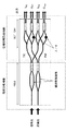
(第2の実施の形態)
図2は本発明の第2の実施の形態の90度光ハイブリッド干渉計の光導波路構成を示す模式図である。図2において、図1と対応する部分は同じ符号が記してある。
As described above, according to this embodiment, it is possible to realize an output port arrangement according to the OIF standard with an optical circuit layout in which the intersections of the optical waveguide arms are reduced.
(Second Embodiment)
FIG. 2 is a schematic diagram showing an optical waveguide configuration of a 90-degree optical hybrid interferometer according to the second embodiment of the present invention. In FIG. 2, the same reference numerals are given to portions corresponding to those in FIG.
第2の実施の形態は、光結合器としていずれもマッハツェンダー干渉計24〜27を用いたものである。また局部発振光にπ/2の位相差を与える光路長を付加する局部発振光導波路アームはアーム9とアーム11とし、マッハツェンダー干渉計24〜27はすべて図中の上側の光導波路部分が長い形状となっている。したがって各マッハツェンダー干渉計の出力干渉特性自体はすべて等しく、出力干渉特性同士の位相差はゼロである。なお信号光導波路アーム3、4、5、6はいずれも干渉計を構成する部分(分岐部から光結合器に達するまで)の長さが等しい。以上のように90度光ハイブリッド干渉計の光回路を構成することにより、その出力干渉特性はOIF標準にしたがった出力ポート配置とすることができる。
In the second embodiment, Mach-
また光結合器としてのマッハツェンダー干渉計24〜27はいずれも同じ側の光導波路部分が長い形状としているため、加工精度の問題等により光結合強度が設計値からずれを生じたとしても、特性に与える影響を抑えることができる。なぜなら加工を行う上で、同一の要因で上記ずれが生じたのであれば、そのずれは少なくとも同じデバイス内であれば、いずれも同じ方向に同じ量で生じると考えられ、出力干渉特性における位相差のずれは相対的にはキャンセルされるからである。
In addition, since the Mach-
以上の構成の光導波回路は、半導体集積回路製造プロセスと同様の微細加工技術により製造することができる。例えばシリコン基板上に積層した屈折率の異なるシリコン酸化膜を、フォトリソグラフィー法を用いて導波路コアやクラッドとしてパターニングすることにより、所定の形状の光導波路を形成できる。図2の構成の光導波回路においては、光導波路アーム3、4、5、6、8、10の長さは、それぞれ分岐部分から光結合器に接続する部分までの長さとして、例えば3mmとする。光導波路アーム9、11は、例えば信号光の中心波長λが1.55μmの場合、他の光導波路アームの長さにλ/4nの値として0.265μmを追加する。ここでnは光導波路の等価屈折率である。またマッハツェンダー干渉計24〜27の幅および光路長差はそれぞれ、例えば780μmおよび0.265μmとする。
The optical waveguide circuit having the above-described configuration can be manufactured by the same microfabrication technique as in the semiconductor integrated circuit manufacturing process. For example, a silicon oxide film having a different refractive index laminated on a silicon substrate is patterned as a waveguide core or a clad by using a photolithography method, whereby an optical waveguide having a predetermined shape can be formed. In the optical waveguide circuit having the configuration shown in FIG. 2, the lengths of the
なお、図2におけるマッハツェンダー干渉計24〜27は、図2の形状とは逆に、すべて図中の下側の光導波路部分が長い形状とした構成にしても、各マッハツェンダー干渉計の出力干渉特性自体に差はないため、やはり上述の場合と同様な好適な効果が得られる。
Note that the Mach-
また、上記の光導波路構成で、光結合器として方向性結合器やマルチモード干渉計などの対称性の光結合器を用いることによっても、やはりOIF標準どおりの出力ポート配置を実現することができる。ただしこれらの90度光ハイブリッド干渉計の各出力干渉信号特性は、それぞれの相対的な位相差関係は一定であるが、光回路や光結合器の構成によって全体の位相自体は異なってくる。 In addition, with the above-described optical waveguide configuration, by using a symmetric optical coupler such as a directional coupler or a multi-mode interferometer as an optical coupler, an output port arrangement as in the OIF standard can also be realized. . However, each output interference signal characteristic of these 90-degree optical hybrid interferometers has a constant relative phase difference relationship, but the entire phase itself varies depending on the configuration of the optical circuit and the optical coupler.
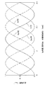
図3(a)〜(e)は、光回路や光結合器の構成が異なる90度光ハイブリッド干渉計の出力ポートからの出力干渉信号特性の位相パターンの比較を示す。これらの図においては、いずれも横軸Δφはマッハツェンダー干渉計に入力される際の信号光と局部発振光との位相差、縦軸は出力強度(a.u.)である。またこれらの図は、比較の便宜のため、いずれもIpおよびQp信号についてのみ表示し、IpおよびQp信号がそれぞれ反転した特性を有するIn及びQn信号に関しては表示を省略した。 3A to 3E show a comparison of phase patterns of output interference signal characteristics from output ports of 90-degree optical hybrid interferometers having different configurations of optical circuits and optical couplers. In these figures, the horizontal axis Δφ is the phase difference between the signal light and the local oscillation light when input to the Mach-Zehnder interferometer, and the vertical axis is the output intensity (au). In these figures, for convenience of comparison, only the Ip and Qp signals are displayed, and the In and Qn signals having the characteristics in which the Ip and Qp signals are inverted are omitted.
図2に示す構成の場合、出力干渉特性は図3(a)のようになり、TE側とTM側とで出力強度の位相自体が同一となる。また図2におけるマッハツェンダー干渉計24〜27の形状を反転し、すべて図中の下側の光導波路部分が長い形状とした構成にした場合は、出力干渉特性は図3(b)のようになり、やはりTE側とTM側とで出力強度の位相自体は同一である。
In the case of the configuration shown in FIG. 2, the output interference characteristic is as shown in FIG. 3A, and the phase of the output intensity itself is the same on the TE side and the TM side. Further, when the shapes of the Mach-
一方、図2におけるマッハツェンダー干渉計24〜27を、方向性結合器やマルチモード干渉計などの対称性の光結合器に置き換えた場合には、出力干渉特性は図3(c)のようになり、TE側とTM側とで出力強度の位相同士は一致していない。
On the other hand, when the Mach-
以上のように、第2の実施の形態では、第1の実施の形態と同様にOIF標準どおりの出力ポート配置を実現しつつ、光導波路アームの交差部を削減できる。そして光結合器としてマッハツェンダー干渉計を用い、そのすべてを同じ側の光導波路部分を長くした構成とすることにより、光結合強度のばらつきの影響を抑制できる。さらにまた、TE側とTM側とで出力干渉特性の位相自体を一致させたい場合には特に好適である。
(第3の実施の形態)
図4は本発明の第3の実施の形態の90度光ハイブリッド干渉計の光導波路構成を示す模式図である。第3の実施の形態は第2の実施の形態と基本的な構成は同様であるが、第3の実施の形態では、局部発振光にπ/2の位相差を与える光路長を付加する局部発振光導波路アームはアーム8とアーム11としている。また光結合器としてマッハツェンダー干渉計24〜27を用い、このうちマッハツェンダー干渉計25だけが図中の下側の光導波路部分が長く、それ以外のものはすべて図中の上側の光導波路部分が長い形状となっている。これにより、マッハツェンダー干渉計25の光結合記としての出力干渉特性は、他のマッハツェンダー干渉計に対して反転した状態、すなわちπの位相差を有する状態となる。したがって、マッハツェンダー干渉計の出力干渉特性の差によって生じる位相差分として、マッハツェンダー干渉計24、26、27についてはゼロ、マッハツェンダー干渉計25についてはπの値を設定する。そしてこれらの値と、アームの位相遅延に対応する位相差との合計で生じる、各出力干渉信号同士の位相差は、IpTEとQpTE、InTEとQnTE、IpTMとQpTM、InTMとQnTM、のいずれもが+π/2となる。
As described above, in the second embodiment, as in the first embodiment, the intersection of the optical waveguide arms can be reduced while realizing the output port arrangement according to the OIF standard. Then, by using a Mach-Zehnder interferometer as an optical coupler and making all of them have a longer optical waveguide portion on the same side, the influence of variations in optical coupling intensity can be suppressed. Furthermore, it is particularly suitable when it is desired to match the phase of the output interference characteristic between the TE side and the TM side.
(Third embodiment)
FIG. 4 is a schematic diagram showing an optical waveguide configuration of a 90-degree optical hybrid interferometer according to the third embodiment of the present invention. The basic configuration of the third embodiment is the same as that of the second embodiment, but in the third embodiment, a local part is added that adds an optical path length that gives a phase difference of π / 2 to the local oscillation light. The oscillation optical waveguide arms are
以上のように90度光ハイブリッド干渉計の光回路を構成することにより、その出力干渉特性はOIF標準にしたがった出力ポート配置とすることができる。なおこの光回路構成では、局部発振光導波路アームの光路長および信号光アームと交差する位置がTE側とTM側とで対称となっている。このため、アームの交差部分による光路長の変動等、設計パラメータ補正の必要が生じた場合において、双方で同様な補正を行えばよく、解析や設計の手間を大幅に省くことができる。 By configuring the optical circuit of the 90-degree optical hybrid interferometer as described above, the output interference characteristic can be set to an output port conforming to the OIF standard. In this optical circuit configuration, the optical path length of the local oscillation optical waveguide arm and the position intersecting with the signal light arm are symmetrical on the TE side and the TM side. For this reason, when there is a need for correction of design parameters such as fluctuations in the optical path length due to the intersection of the arms, the same correction may be performed on both sides, and the labor of analysis and design can be saved greatly.
上述の効果は、図4におけるマッハツェンダー干渉計24〜27を、それぞれ光導波路を長くする側をすべて反転させた形状のものに置き換えても、同様に得ることができる。
The above-described effects can be obtained in the same manner by replacing the Mach-
なお、図4に示す構成の場合、90度光ハイブリッド干渉計の出力ポートからの出力干渉特性は図3(d)のようになる。 In the case of the configuration shown in FIG. 4, the output interference characteristic from the output port of the 90-degree optical hybrid interferometer is as shown in FIG.
以上のように、第3の実施の形態では、第1、第2の実施の形態と同様にOIF標準どおりの出力ポート配置を実現しつつ、光導波路アームの交差部を削減できる。そして局部発振光導波路アーム構造がTE側とTM側とで対照となっていることから、設計パラメータ補正の必要が生じた場合にも、解析や設計の手間を大幅に省くことができる。
(第4の実施の形態)
図5は本発明の第4の実施の形態の90度光ハイブリッド干渉計の光導波路構成を示す模式図である。第4の実施の形態は、第3の実施の形態の変形例であり、局部発振光にπ/2の位相差を与える光路長を付加する局部発振光導波路アームはアーム9とアーム10としている。また光結合器としてマッハツェンダー干渉計24〜27を用い、このうちマッハツェンダー干渉計27だけが図中の下側の光導波路が長く、それ以外のものはすべて図中の上側の光導波路が長い形状となっている。以上のように90度光ハイブリッド干渉計の光回路を構成することにより、その出力干渉特性はOIF標準にしたがった出力ポート配置とすることができる。なおこの光回路構成では、第3の実施の形態と同様、局部発振光導波路アームの光路長および信号光アームと交差する位置がTE側とTM側とで対称となっている。このため、やはりアームの交差部分による光路長の変動等、設計パラメータ補正の必要が生じた場合において、双方で同様な補正を行えばよく、解析や設計の手間を大幅に省くことができる。
As described above, in the third embodiment, as in the first and second embodiments, the intersection of the optical waveguide arms can be reduced while realizing the output port arrangement according to the OIF standard. Since the locally oscillating optical waveguide arm structure is contrasted between the TE side and the TM side, it is possible to greatly reduce the labor of analysis and design even when the design parameter needs to be corrected.
(Fourth embodiment)
FIG. 5 is a schematic diagram showing an optical waveguide configuration of a 90-degree optical hybrid interferometer according to a fourth embodiment of the present invention. The fourth embodiment is a modification of the third embodiment, and the local oscillation optical waveguide arms that add an optical path length that gives a phase difference of π / 2 to the local oscillation light are the
上述の効果は、図5におけるマッハツェンダー干渉計24〜27を、それぞれ光導波路を長くする側をすべて反転させた形状のものに置き換えても、同様に得ることができる。
The above-described effects can be similarly obtained even if the Mach-
なお、図5に示す構成の場合、90度光ハイブリッド干渉計の出力ポートからの出力干渉特性は図3(e)のようになる。 In the case of the configuration shown in FIG. 5, the output interference characteristic from the output port of the 90-degree optical hybrid interferometer is as shown in FIG.
以上のように、第4の実施の形態では、第1〜3の実施の形態と同様にOIF標準どおりの出力ポート配置を実現しつつ、光導波路アームの交差部を削減できる。そして局部発振光導波路アーム構造がTE側とTM側とで対称となっていることから、設計パラメータ補正の必要が生じた場合にも、解析や設計の手間を大幅に省くことができる。 As described above, in the fourth embodiment, the intersections of the optical waveguide arms can be reduced while realizing the output port arrangement according to the OIF standard as in the first to third embodiments. Since the local oscillation optical waveguide arm structure is symmetric between the TE side and the TM side, it is possible to greatly reduce the labor of analysis and design even when design parameter correction is required.
1 TE信号光入力ポート
2 TM信号光入力ポート
3〜6 信号光導波路アーム
7 局部発振光入力ポート
8〜11 局部発振光導波路アーム
12〜15 光結合器
16〜23 出力ポート
24〜27 マッハツェンダー干渉計
1 TE signal
Claims (8)
前記偏波分離したTE光信号およびTM光信号をそれぞれ入力する2つの信号光入力ポートと、
前記2つの信号光入力ポートの間に配置された、局部発振光を入力する局部発振光入力ポートと、
前記信号光入力ポートから入力され、それぞれI相側とQ相側とに2分岐された、前記TE光信号およびTM光信号を伝播する信号光導波路アームと、
前記局部発振光入力ポートから入力され、前記TE光信号側と前記TM光信号側とに2分岐された後、さらにそれぞれ2つに分岐された前記局部発振光を伝播する局部発振光導波路アームと、
前記TE光信号側においてI相側とQ相側とに2分岐した前記TE光信号と、前記TE光信号側において2つに分岐された前記局部発振光とを、それぞれ一対ずつ結合する2つの光結合器と、
前記TM光信号側においてI相側とQ相側とに2分岐した前記TM光信号と、前記TM光信号側において2つに分岐された前記局部発振光とを、それぞれ一対ずつ結合する2つの光結合器と、
前記TE光信号側およびTM光信号側のそれぞれにおいて、2つの前記光結合器から出力される、対をなす信号光と局部発振光との位相差による4つの干渉信号を、それぞれ前記位相情報Ip、In、Qp、Qnとして取り出す4つの出力ポートと、
を有し、
前記TE光信号側および前記TM光信号側のそれぞれにおいて、前記I相側と前記Q相側のいずれか一方の、前記信号光導波路アームと前記局部発振光導波路アームとの対に、光路長差を設けることにより、前記I相側と前記Q相側の出力干渉信号IpとQp、並びにInとQnとの間にそれぞれ前記光路長差に対応する遅延位相差を与え、
前記TE光信号側および前記TM光信号側のそれぞれにおいて、前記I相側の光結合器と前記Q相側の光結合器とがそれぞれ有する出力干渉特性同士の位相差と、前記遅延位相差とを、両者の合計で生じる、出力干渉信号Ipに対するQpの出力位相差、並びに出力干渉信号Inに対するQnの出力位相差が、共に+π/2となるように設定することにより、8つの前記出力ポートの出力信号を、上から前記TE光信号側のIp、In、Qp、Qn、および前記TM光信号側のIp、In、Qp、Qnの順に配列したことを特徴とする、90度光ハイブリッド干渉計。 From phase-separated Transverse Electric (TE) optical signal and Transverse Magnetic (T M ) optical signal, phase information Ip and In having a phase difference of π from each other, and π / 2 with respect to Ip and In, respectively. A 90 degree optical hybrid interferometer for extracting quaternary phase information on the IQ plane, comprising phase information Qp and Qn having a phase delay of
Two signal light input ports for inputting the polarization-separated TE optical signal and TM optical signal,
A local oscillation light input port for inputting local oscillation light, disposed between the two signal light input ports;
A signal optical waveguide arm that propagates the TE optical signal and the TM optical signal, which is input from the signal light input port and bifurcated into an I-phase side and a Q-phase side, respectively;
A local oscillation optical waveguide arm which is input from the local oscillation light input port, and is branched into two branches on the TE optical signal side and the TM optical signal side, and then propagates the local oscillation light further branched into two, respectively; ,
Wherein the TE optical signal 2 branches into a Oite I-phase side and the Q-phase side to the TE optical signal side, and the local oscillator beam branched into two in the TE optical signal side, respectively coupled in pairs Two optical couplers;
Wherein the TM light signals 2 branches into a Oite I-phase side and the Q-phase side to the TM optical signal side and the TM optical signal side the local oscillator beam branched into two at, respectively coupled in pairs Two optical couplers;
On each of the TE optical signal side and the TM optical signal side, four interference signals, which are output from the two optical couplers and are based on the phase difference between the paired signal light and the local oscillation light, are respectively referred to as the phase information Ip. , Four output ports to be taken out as In, Qp, and Qn,
Have
In each of the TE optical signal side and the TM optical signal side, there is an optical path length difference between the signal optical waveguide arm and the local oscillation optical waveguide arm on either the I-phase side or the Q-phase side. By providing a delay phase difference corresponding to the optical path length difference between the I-phase side and the Q-phase side output interference signals Ip and Qp, and In and Qn,
In each of the TE optical signal side and the TM optical signal side, a phase difference between output interference characteristics of the I-phase side optical coupler and the Q-phase side optical coupler, and the delay phase difference, Are set so that the output phase difference of Qp with respect to the output interference signal Ip and the output phase difference of Qn with respect to the output interference signal In are both + π / 2. The 90 ° optical hybrid interference is characterized in that Ip, In, Qp, Qn on the TE optical signal side and Ip, In, Qp, Qn on the TM optical signal side are arranged in this order from above. Total.
前記偏波分離したTE光信号およびTM光信号をそれぞれ入力する2つの信号光入力ポートと、
前記2つの信号光入力ポートの間に配置された、局部発振光を入力する局部発振光入力ポートと、
前記信号光入力ポートから入力され、それぞれI相側とQ相側とに2分岐された、前記TE光信号およびTM光信号を伝播する信号光導波路アームと、
前記局部発振光入力ポートから入力され、前記TE光信号側と前記TM光信号側とに2分岐された後、さらにそれぞれ2つに分岐された前記局部発振光を伝播する局部発振光導波路アームと、
前記TE光信号側においてI相側とQ相側とに2分岐した前記TE光信号と、前記TE光信号側において2つに分岐された前記局部発振光とを、それぞれ一対ずつ結合する2つの光結合器と、
前記TM光信号側においてI相側とQ相側とに2分岐した前記TM光信号と、前記TM光信号側において2つに分岐された前記局部発振光とを、それぞれ一対ずつ結合する2つの光結合器と、
前記TE光信号側およびTM光信号側のそれぞれにおいて、2つの前記光結合器から出力される、対をなす信号光と局部発振光との位相差による4つの干渉信号を、それぞれ前記位相情報Ip、In、Qp、Qnとして取り出す4つの出力ポートと、
を構成し、
前記TE光信号側および前記TM光信号側のそれぞれにおいて、前記I相側と前記Q相側のいずれか一方の、前記信号光導波路アームと前記局部発振光導波路アームとの対に、光路長差を設けることにより、前記I相側と前記Q相側の出力干渉信号IpとQp、並びにInとQnとの間にそれぞれ前記光路長差に対応する遅延位相差を与え、
前記TE光信号側および前記TM光信号側のそれぞれにおいて、前記I相側の光結合器と前記Q相側の光結合器とがそれぞれ有する出力干渉特性同士の位相差と、前記遅延位相差とを、両者の合計で生じる、出力干渉信号Ipに対するQpの出力位相差、並びに出力干渉信号Inに対するQnの出力位相差が、共に+π/2となるように設定することにより、8つの前記出力ポートの出力信号を、上から前記TE光信号側のIp、In、Qp、Qn、および前記TM光信号側のIp、In、Qp、Qnの順に配列することを特徴とする、90度光ハイブリッド干渉計の製造方法。 From phase-separated Transverse Electric (TE) optical signal and Transverse Magnetic (T M ) optical signal, phase information Ip and In having a phase difference of π from each other, and π / 2 with respect to Ip and In, respectively. A 90-degree optical hybrid interferometer manufacturing method for extracting quaternary phase information on the IQ plane, comprising phase information Qp and Qn having a phase delay of:
Two signal light input ports for inputting the polarization-separated TE optical signal and TM optical signal,
A local oscillation light input port for inputting local oscillation light, disposed between the two signal light input ports;
A signal optical waveguide arm that propagates the TE optical signal and the TM optical signal, which is input from the signal light input port and bifurcated into an I-phase side and a Q-phase side, respectively;
A local oscillation optical waveguide arm which is input from the local oscillation light input port, and is branched into two branches on the TE optical signal side and the TM optical signal side, and then propagates the local oscillation light further branched into two, respectively; ,
Wherein the TE optical signal 2 branches into a Oite I-phase side and the Q-phase side to the TE optical signal side, and the local oscillator beam branched into two in the TE optical signal side, respectively coupled in pairs Two optical couplers;
Wherein the TM light signals 2 branches into a Oite I-phase side and the Q-phase side to the TM optical signal side and the TM optical signal side the local oscillator beam branched into two at, respectively coupled in pairs Two optical couplers;
On each of the TE optical signal side and the TM optical signal side, four interference signals, which are output from the two optical couplers and are based on the phase difference between the paired signal light and the local oscillation light, are respectively referred to as the phase information Ip. , Four output ports to be taken out as In, Qp, and Qn,
Configure
In each of the TE optical signal side and the TM optical signal side, there is an optical path length difference between the signal optical waveguide arm and the local oscillation optical waveguide arm on either the I-phase side or the Q-phase side. By providing a delay phase difference corresponding to the optical path length difference between the I-phase side and the Q-phase side output interference signals Ip and Qp, and In and Qn,
In each of the TE optical signal side and the TM optical signal side, a phase difference between output interference characteristics of the I-phase side optical coupler and the Q-phase side optical coupler, and the delay phase difference, Are set so that the output phase difference of Qp with respect to the output interference signal Ip and the output phase difference of Qn with respect to the output interference signal In are both + π / 2. The 90 ° optical hybrid interference is characterized in that Ip, In, Qp, Qn on the TE optical signal side and Ip, In, Qp, Qn on the TM optical signal side are arranged in this order from the top. Total manufacturing method.
Priority Applications (3)
| Application Number | Priority Date | Filing Date | Title |
|---|---|---|---|
| JP2010064473A JP5598043B2 (en) | 2010-03-19 | 2010-03-19 | 90-degree optical hybrid interferometer and manufacturing method of 90-degree optical hybrid interferometer |
| US13/034,923 US8478090B2 (en) | 2010-03-19 | 2011-02-25 | Optical waveguide device and manufacturing method of optical waveguide device |
| CN201110068771.0A CN102193144B (en) | 2010-03-19 | 2011-03-18 | Optical waveguide device and manufacturing method of optical waveguide device |
Applications Claiming Priority (1)
| Application Number | Priority Date | Filing Date | Title |
|---|---|---|---|
| JP2010064473A JP5598043B2 (en) | 2010-03-19 | 2010-03-19 | 90-degree optical hybrid interferometer and manufacturing method of 90-degree optical hybrid interferometer |
Publications (2)
| Publication Number | Publication Date |
|---|---|
| JP2011197433A JP2011197433A (en) | 2011-10-06 |
| JP5598043B2 true JP5598043B2 (en) | 2014-10-01 |
Family
ID=44601538
Family Applications (1)
| Application Number | Title | Priority Date | Filing Date |
|---|---|---|---|
| JP2010064473A Active JP5598043B2 (en) | 2010-03-19 | 2010-03-19 | 90-degree optical hybrid interferometer and manufacturing method of 90-degree optical hybrid interferometer |
Country Status (3)
| Country | Link |
|---|---|
| US (1) | US8478090B2 (en) |
| JP (1) | JP5598043B2 (en) |
| CN (1) | CN102193144B (en) |
Families Citing this family (6)
| Publication number | Priority date | Publication date | Assignee | Title |
|---|---|---|---|---|
| CN104160641B (en) * | 2012-03-06 | 2016-09-14 | 日本电气株式会社 | Planar light wave circuit and optical receiver |
| EP2709295A1 (en) * | 2012-09-14 | 2014-03-19 | Alcatel Lucent | Visualisation of an optical signal by linear optical sampling |
| WO2015096159A1 (en) * | 2013-12-27 | 2015-07-02 | 华为技术有限公司 | Optical signal control method, and optical switch matrix control method and device |
| JP6346803B2 (en) * | 2014-06-23 | 2018-06-20 | 株式会社フジクラ | Optical receiver circuit and adjustment method thereof |
| JP6919557B2 (en) * | 2017-12-26 | 2021-08-18 | 住友電気工業株式会社 | 90 degree optical hybrid integrated circuit |
| US10731383B2 (en) * | 2018-08-01 | 2020-08-04 | Macom Technology Solutions Holdings, Inc. | Symmetric coherent optical mixer |
Family Cites Families (12)
| Publication number | Priority date | Publication date | Assignee | Title |
|---|---|---|---|---|
| US5703975A (en) * | 1995-06-09 | 1997-12-30 | Corning Incorporated | Interferometric switch |
| KR100310086B1 (en) * | 1998-11-17 | 2002-11-27 | 삼성전자 주식회사 | Optical coupler and its manufacturing method |
| US7245432B2 (en) * | 2001-03-28 | 2007-07-17 | Main Street Ventures, Llc | Dual diffraction-grating device |
| US7174069B2 (en) * | 2001-03-28 | 2007-02-06 | Main Street Ventures Llc | All optical multiplexer |
| US7460793B2 (en) * | 2002-12-11 | 2008-12-02 | Michael George Taylor | Coherent optical detection and signal processing method and system |
| US7555227B2 (en) * | 2005-10-21 | 2009-06-30 | Nortel Networks Limited | Polarization compensation in a coherent optical receiver |
| JP5042701B2 (en) * | 2007-05-01 | 2012-10-03 | 日本電信電話株式会社 | Optical sampling apparatus and optical sampling method |
| JP5340004B2 (en) * | 2008-06-18 | 2013-11-13 | 株式会社日立製作所 | Balance compensation type optical balanced receiver and optical IQ receiver |
| JP5287527B2 (en) * | 2008-12-26 | 2013-09-11 | 富士通株式会社 | Optical hybrid circuit, optical receiver and optical receiving method |
| JP5326584B2 (en) * | 2009-01-09 | 2013-10-30 | 富士通株式会社 | Delay processing device, signal amplification device, photoelectric conversion device, analog / digital conversion device, reception device, and reception method |
| WO2011027895A1 (en) * | 2009-09-07 | 2011-03-10 | 古河電気工業株式会社 | Plc type demodulator and optical transmission system |
| US8705900B2 (en) * | 2010-03-19 | 2014-04-22 | Nippon Telegraph And Telephone Corporation | Optical modulator |
-
2010
- 2010-03-19 JP JP2010064473A patent/JP5598043B2/en active Active
-
2011
- 2011-02-25 US US13/034,923 patent/US8478090B2/en active Active
- 2011-03-18 CN CN201110068771.0A patent/CN102193144B/en active Active
Also Published As
| Publication number | Publication date |
|---|---|
| JP2011197433A (en) | 2011-10-06 |
| CN102193144A (en) | 2011-09-21 |
| CN102193144B (en) | 2014-09-24 |
| US8478090B2 (en) | 2013-07-02 |
| US20110229075A1 (en) | 2011-09-22 |
Similar Documents
| Publication | Publication Date | Title |
|---|---|---|
| US9103985B2 (en) | Optical waveguide device and a manufacturing method for an optical waveguide device | |
| US8526102B2 (en) | PLC-type demodulator and optical transmission system | |
| JP5287527B2 (en) | Optical hybrid circuit, optical receiver and optical receiving method | |
| JP5402802B2 (en) | Optical waveguide circuit and method of manufacturing optical waveguide circuit | |
| US8649643B2 (en) | Optical hybrid circuit and optical receiver | |
| JP5598043B2 (en) | 90-degree optical hybrid interferometer and manufacturing method of 90-degree optical hybrid interferometer | |
| JP5373901B2 (en) | Optical 90 degree hybrid circuit | |
| JPWO2016194349A1 (en) | Optical coherent mixer circuit | |
| WO2012153857A1 (en) | Optical mixer, optical receiver, optical mixing method, and production method for optical mixer | |
| US10444430B2 (en) | Optical waveguide structure and optical waveguide circuit | |
| JP7380329B2 (en) | Optical circuit devices and optical receivers | |
| JP7425357B2 (en) | optical circuit | |
| CN114365033A (en) | IQ optical modulator | |
| US11982839B2 (en) | Optical 90 degree hybrid circuit | |
| JP6704436B2 (en) | Optical hybrid circuit | |
| JP6476264B1 (en) | Optical hybrid circuit | |
| JP2021057749A (en) | Coherent detection element | |
| WO2016060263A1 (en) | Integrated optical coupler having polarization separation/synthesis function | |
| JP2017058603A (en) | Optical waveguide element |
Legal Events
| Date | Code | Title | Description |
|---|---|---|---|
| RD01 | Notification of change of attorney |
Free format text: JAPANESE INTERMEDIATE CODE: A7421 Effective date: 20110707 |
|
| A621 | Written request for application examination |
Free format text: JAPANESE INTERMEDIATE CODE: A621 Effective date: 20130218 |
|
| A131 | Notification of reasons for refusal |
Free format text: JAPANESE INTERMEDIATE CODE: A131 Effective date: 20140128 |
|
| A521 | Request for written amendment filed |
Free format text: JAPANESE INTERMEDIATE CODE: A523 Effective date: 20140327 |
|
| TRDD | Decision of grant or rejection written | ||
| A01 | Written decision to grant a patent or to grant a registration (utility model) |
Free format text: JAPANESE INTERMEDIATE CODE: A01 Effective date: 20140715 |
|
| A61 | First payment of annual fees (during grant procedure) |
Free format text: JAPANESE INTERMEDIATE CODE: A61 Effective date: 20140728 |
|
| R150 | Certificate of patent or registration of utility model |
Ref document number: 5598043 Country of ref document: JP Free format text: JAPANESE INTERMEDIATE CODE: R150 |