JP5590886B2 - Fluorine plasma treatment for high-K gate stacks for defect passivation - Google Patents
Fluorine plasma treatment for high-K gate stacks for defect passivation Download PDFInfo
- Publication number
- JP5590886B2 JP5590886B2 JP2009530575A JP2009530575A JP5590886B2 JP 5590886 B2 JP5590886 B2 JP 5590886B2 JP 2009530575 A JP2009530575 A JP 2009530575A JP 2009530575 A JP2009530575 A JP 2009530575A JP 5590886 B2 JP5590886 B2 JP 5590886B2
- Authority
- JP
- Japan
- Prior art keywords
- substrate
- plasma
- dielectric layer
- fluorine
- processing chamber
- Prior art date
- Legal status (The legal status is an assumption and is not a legal conclusion. Google has not performed a legal analysis and makes no representation as to the accuracy of the status listed.)
- Active
Links
- 229910052731 fluorine Inorganic materials 0.000 title claims description 32
- YCKRFDGAMUMZLT-UHFFFAOYSA-N Fluorine atom Chemical compound [F] YCKRFDGAMUMZLT-UHFFFAOYSA-N 0.000 title claims description 31
- 239000011737 fluorine Substances 0.000 title claims description 31
- 230000007547 defect Effects 0.000 title claims description 6
- 238000002161 passivation Methods 0.000 title 1
- 238000009832 plasma treatment Methods 0.000 title 1
- 239000000758 substrate Substances 0.000 claims description 94
- 238000000034 method Methods 0.000 claims description 92
- 239000007789 gas Substances 0.000 claims description 57
- 230000008569 process Effects 0.000 claims description 56
- 239000000463 material Substances 0.000 claims description 30
- 238000000137 annealing Methods 0.000 claims description 16
- 229910052735 hafnium Inorganic materials 0.000 claims description 14
- VBJZVLUMGGDVMO-UHFFFAOYSA-N hafnium atom Chemical compound [Hf] VBJZVLUMGGDVMO-UHFFFAOYSA-N 0.000 claims description 13
- 150000002500 ions Chemical class 0.000 claims description 10
- 229910052751 metal Inorganic materials 0.000 claims description 10
- 239000002184 metal Substances 0.000 claims description 10
- IJGRMHOSHXDMSA-UHFFFAOYSA-N Atomic nitrogen Chemical compound N#N IJGRMHOSHXDMSA-UHFFFAOYSA-N 0.000 claims description 9
- XKRFYHLGVUSROY-UHFFFAOYSA-N Argon Chemical compound [Ar] XKRFYHLGVUSROY-UHFFFAOYSA-N 0.000 claims description 8
- QVGXLLKOCUKJST-UHFFFAOYSA-N atomic oxygen Chemical compound [O] QVGXLLKOCUKJST-UHFFFAOYSA-N 0.000 claims description 7
- 229910052760 oxygen Inorganic materials 0.000 claims description 7
- 239000001301 oxygen Substances 0.000 claims description 7
- 239000001307 helium Substances 0.000 claims description 6
- 229910052734 helium Inorganic materials 0.000 claims description 6
- SWQJXJOGLNCZEY-UHFFFAOYSA-N helium atom Chemical compound [He] SWQJXJOGLNCZEY-UHFFFAOYSA-N 0.000 claims description 6
- 229910052757 nitrogen Inorganic materials 0.000 claims description 6
- OKTJSMMVPCPJKN-UHFFFAOYSA-N Carbon Chemical compound [C] OKTJSMMVPCPJKN-UHFFFAOYSA-N 0.000 claims description 5
- RTAQQCXQSZGOHL-UHFFFAOYSA-N Titanium Chemical compound [Ti] RTAQQCXQSZGOHL-UHFFFAOYSA-N 0.000 claims description 5
- 229910052799 carbon Inorganic materials 0.000 claims description 5
- 238000005530 etching Methods 0.000 claims description 5
- 230000006698 induction Effects 0.000 claims description 5
- 239000004065 semiconductor Substances 0.000 claims description 5
- 229910052715 tantalum Inorganic materials 0.000 claims description 5
- GUVRBAGPIYLISA-UHFFFAOYSA-N tantalum atom Chemical compound [Ta] GUVRBAGPIYLISA-UHFFFAOYSA-N 0.000 claims description 5
- 229910052719 titanium Inorganic materials 0.000 claims description 5
- 239000010936 titanium Substances 0.000 claims description 5
- 229910052721 tungsten Inorganic materials 0.000 claims description 5
- 239000010937 tungsten Substances 0.000 claims description 5
- -1 tungsten nitride Chemical class 0.000 claims description 5
- BPQQTUXANYXVAA-UHFFFAOYSA-N Orthosilicate Chemical compound [O-][Si]([O-])([O-])[O-] BPQQTUXANYXVAA-UHFFFAOYSA-N 0.000 claims description 4
- NRTOMJZYCJJWKI-UHFFFAOYSA-N Titanium nitride Chemical compound [Ti]#N NRTOMJZYCJJWKI-UHFFFAOYSA-N 0.000 claims description 4
- 229910052786 argon Inorganic materials 0.000 claims description 4
- 229910000449 hafnium oxide Inorganic materials 0.000 claims description 4
- WIHZLLGSGQNAGK-UHFFFAOYSA-N hafnium(4+);oxygen(2-) Chemical compound [O-2].[O-2].[Hf+4] WIHZLLGSGQNAGK-UHFFFAOYSA-N 0.000 claims description 4
- MRELNEQAGSRDBK-UHFFFAOYSA-N lanthanum(3+);oxygen(2-) Chemical compound [O-2].[O-2].[O-2].[La+3].[La+3] MRELNEQAGSRDBK-UHFFFAOYSA-N 0.000 claims description 4
- RVTZCBVAJQQJTK-UHFFFAOYSA-N oxygen(2-);zirconium(4+) Chemical compound [O-2].[O-2].[Zr+4] RVTZCBVAJQQJTK-UHFFFAOYSA-N 0.000 claims description 4
- 229910001928 zirconium oxide Inorganic materials 0.000 claims description 4
- 230000001939 inductive effect Effects 0.000 claims description 3
- MZLGASXMSKOWSE-UHFFFAOYSA-N tantalum nitride Chemical compound [Ta]#N MZLGASXMSKOWSE-UHFFFAOYSA-N 0.000 claims description 3
- DBOSVWZVMLOAEU-UHFFFAOYSA-N [O-2].[Hf+4].[La+3] Chemical compound [O-2].[Hf+4].[La+3] DBOSVWZVMLOAEU-UHFFFAOYSA-N 0.000 claims description 2
- TWNQGVIAIRXVLR-UHFFFAOYSA-N oxo(oxoalumanyloxy)alumane Chemical compound O=[Al]O[Al]=O TWNQGVIAIRXVLR-UHFFFAOYSA-N 0.000 claims description 2
- WFKWXMTUELFFGS-UHFFFAOYSA-N tungsten Chemical compound [W] WFKWXMTUELFFGS-UHFFFAOYSA-N 0.000 claims description 2
- 239000012080 ambient air Substances 0.000 claims 2
- 239000003989 dielectric material Substances 0.000 description 28
- 238000000151 deposition Methods 0.000 description 24
- 238000003682 fluorination reaction Methods 0.000 description 20
- 150000001875 compounds Chemical class 0.000 description 14
- XUIMIQQOPSSXEZ-UHFFFAOYSA-N Silicon Chemical compound [Si] XUIMIQQOPSSXEZ-UHFFFAOYSA-N 0.000 description 13
- 229910052710 silicon Inorganic materials 0.000 description 13
- 239000010703 silicon Substances 0.000 description 13
- 238000000231 atomic layer deposition Methods 0.000 description 11
- 238000004140 cleaning Methods 0.000 description 11
- 239000002243 precursor Substances 0.000 description 11
- 230000008021 deposition Effects 0.000 description 10
- 238000006243 chemical reaction Methods 0.000 description 9
- 238000005229 chemical vapour deposition Methods 0.000 description 9
- 239000002019 doping agent Substances 0.000 description 9
- 235000012431 wafers Nutrition 0.000 description 9
- VYPSYNLAJGMNEJ-UHFFFAOYSA-N Silicium dioxide Chemical compound O=[Si]=O VYPSYNLAJGMNEJ-UHFFFAOYSA-N 0.000 description 7
- 230000015572 biosynthetic process Effects 0.000 description 7
- 238000010586 diagram Methods 0.000 description 7
- 238000010926 purge Methods 0.000 description 7
- 229910021420 polycrystalline silicon Inorganic materials 0.000 description 6
- 229920005591 polysilicon Polymers 0.000 description 6
- 238000010438 heat treatment Methods 0.000 description 5
- ZOXJGFHDIHLPTG-UHFFFAOYSA-N Boron Chemical compound [B] ZOXJGFHDIHLPTG-UHFFFAOYSA-N 0.000 description 4
- 229940126062 Compound A Drugs 0.000 description 4
- NLDMNSXOCDLTTB-UHFFFAOYSA-N Heterophylliin A Natural products O1C2COC(=O)C3=CC(O)=C(O)C(O)=C3C3=C(O)C(O)=C(O)C=C3C(=O)OC2C(OC(=O)C=2C=C(O)C(O)=C(O)C=2)C(O)C1OC(=O)C1=CC(O)=C(O)C(O)=C1 NLDMNSXOCDLTTB-UHFFFAOYSA-N 0.000 description 4
- 239000012298 atmosphere Substances 0.000 description 4
- 229910052796 boron Inorganic materials 0.000 description 4
- 238000011065 in-situ storage Methods 0.000 description 4
- 239000011261 inert gas Substances 0.000 description 4
- 238000004518 low pressure chemical vapour deposition Methods 0.000 description 4
- 229910052726 zirconium Inorganic materials 0.000 description 4
- 229910018072 Al 2 O 3 Inorganic materials 0.000 description 3
- 229910004129 HfSiO Inorganic materials 0.000 description 3
- OAICVXFJPJFONN-UHFFFAOYSA-N Phosphorus Chemical compound [P] OAICVXFJPJFONN-UHFFFAOYSA-N 0.000 description 3
- 229910004298 SiO 2 Inorganic materials 0.000 description 3
- QCWXUUIWCKQGHC-UHFFFAOYSA-N Zirconium Chemical compound [Zr] QCWXUUIWCKQGHC-UHFFFAOYSA-N 0.000 description 3
- 229910007880 ZrAl Inorganic materials 0.000 description 3
- CSDREXVUYHZDNP-UHFFFAOYSA-N alumanylidynesilicon Chemical compound [Al].[Si] CSDREXVUYHZDNP-UHFFFAOYSA-N 0.000 description 3
- 125000004429 atom Chemical group 0.000 description 3
- 238000011109 contamination Methods 0.000 description 3
- 238000005137 deposition process Methods 0.000 description 3
- 239000012535 impurity Substances 0.000 description 3
- 239000000203 mixture Substances 0.000 description 3
- 229910052698 phosphorus Inorganic materials 0.000 description 3
- 239000011574 phosphorus Substances 0.000 description 3
- 229910052814 silicon oxide Inorganic materials 0.000 description 3
- 230000000087 stabilizing effect Effects 0.000 description 3
- OGIDPMRJRNCKJF-UHFFFAOYSA-N titanium oxide Inorganic materials [Ti]=O OGIDPMRJRNCKJF-UHFFFAOYSA-N 0.000 description 3
- 229910000789 Aluminium-silicon alloy Inorganic materials 0.000 description 2
- 229910021193 La 2 O 3 Inorganic materials 0.000 description 2
- 229910006249 ZrSi Inorganic materials 0.000 description 2
- YKTSYUJCYHOUJP-UHFFFAOYSA-N [O--].[Al+3].[Al+3].[O-][Si]([O-])([O-])[O-] Chemical compound [O--].[Al+3].[Al+3].[O-][Si]([O-])([O-])[O-] YKTSYUJCYHOUJP-UHFFFAOYSA-N 0.000 description 2
- 229910052782 aluminium Inorganic materials 0.000 description 2
- XAGFODPZIPBFFR-UHFFFAOYSA-N aluminium Chemical compound [Al] XAGFODPZIPBFFR-UHFFFAOYSA-N 0.000 description 2
- 229910052785 arsenic Inorganic materials 0.000 description 2
- RQNWIZPPADIBDY-UHFFFAOYSA-N arsenic atom Chemical compound [As] RQNWIZPPADIBDY-UHFFFAOYSA-N 0.000 description 2
- 238000003877 atomic layer epitaxy Methods 0.000 description 2
- WTEOIRVLGSZEPR-UHFFFAOYSA-N boron trifluoride Chemical compound FB(F)F WTEOIRVLGSZEPR-UHFFFAOYSA-N 0.000 description 2
- 239000002826 coolant Substances 0.000 description 2
- 238000001816 cooling Methods 0.000 description 2
- 229910052746 lanthanum Inorganic materials 0.000 description 2
- FZLIPJUXYLNCLC-UHFFFAOYSA-N lanthanum atom Chemical compound [La] FZLIPJUXYLNCLC-UHFFFAOYSA-N 0.000 description 2
- 239000010410 layer Substances 0.000 description 2
- 150000004767 nitrides Chemical class 0.000 description 2
- 230000006911 nucleation Effects 0.000 description 2
- 238000010899 nucleation Methods 0.000 description 2
- 230000003647 oxidation Effects 0.000 description 2
- 238000007254 oxidation reaction Methods 0.000 description 2
- 238000005240 physical vapour deposition Methods 0.000 description 2
- 238000000623 plasma-assisted chemical vapour deposition Methods 0.000 description 2
- 238000002203 pretreatment Methods 0.000 description 2
- 230000009467 reduction Effects 0.000 description 2
- 235000012239 silicon dioxide Nutrition 0.000 description 2
- 239000000377 silicon dioxide Substances 0.000 description 2
- 238000001179 sorption measurement Methods 0.000 description 2
- 238000000992 sputter etching Methods 0.000 description 2
- 239000000126 substance Substances 0.000 description 2
- JBRZTFJDHDCESZ-UHFFFAOYSA-N AsGa Chemical compound [As]#[Ga] JBRZTFJDHDCESZ-UHFFFAOYSA-N 0.000 description 1
- 229910015900 BF3 Inorganic materials 0.000 description 1
- 229910001218 Gallium arsenide Inorganic materials 0.000 description 1
- UFHFLCQGNIYNRP-UHFFFAOYSA-N Hydrogen Chemical compound [H][H] UFHFLCQGNIYNRP-UHFFFAOYSA-N 0.000 description 1
- 229910017414 LaAl Inorganic materials 0.000 description 1
- 229910052581 Si3N4 Inorganic materials 0.000 description 1
- 229910000577 Silicon-germanium Inorganic materials 0.000 description 1
- 229910010413 TiO 2 Inorganic materials 0.000 description 1
- GWEVSGVZZGPLCZ-UHFFFAOYSA-N Titan oxide Chemical compound O=[Ti]=O GWEVSGVZZGPLCZ-UHFFFAOYSA-N 0.000 description 1
- 229910006501 ZrSiO Inorganic materials 0.000 description 1
- ZGUQGPFMMTZGBQ-UHFFFAOYSA-N [Al].[Al].[Zr] Chemical compound [Al].[Al].[Zr] ZGUQGPFMMTZGBQ-UHFFFAOYSA-N 0.000 description 1
- SLODBEHWNYQCRC-UHFFFAOYSA-N [La+3].[O-2].[Zr+4] Chemical compound [La+3].[O-2].[Zr+4] SLODBEHWNYQCRC-UHFFFAOYSA-N 0.000 description 1
- LEVVHYCKPQWKOP-UHFFFAOYSA-N [Si].[Ge] Chemical compound [Si].[Ge] LEVVHYCKPQWKOP-UHFFFAOYSA-N 0.000 description 1
- SDXDHLDNCJPIJZ-UHFFFAOYSA-N [Zr].[Zr] Chemical compound [Zr].[Zr] SDXDHLDNCJPIJZ-UHFFFAOYSA-N 0.000 description 1
- 230000009471 action Effects 0.000 description 1
- 230000002411 adverse Effects 0.000 description 1
- 150000004645 aluminates Chemical class 0.000 description 1
- BOIGHUSRADNYQR-UHFFFAOYSA-N aluminum;lanthanum(3+);oxygen(2-) Chemical compound [O-2].[O-2].[O-2].[Al+3].[La+3] BOIGHUSRADNYQR-UHFFFAOYSA-N 0.000 description 1
- 229910021417 amorphous silicon Inorganic materials 0.000 description 1
- 229910052787 antimony Inorganic materials 0.000 description 1
- WATWJIUSRGPENY-UHFFFAOYSA-N antimony atom Chemical compound [Sb] WATWJIUSRGPENY-UHFFFAOYSA-N 0.000 description 1
- 230000004888 barrier function Effects 0.000 description 1
- 239000006227 byproduct Substances 0.000 description 1
- 239000003990 capacitor Substances 0.000 description 1
- 239000002131 composite material Substances 0.000 description 1
- 239000004020 conductor Substances 0.000 description 1
- 239000000356 contaminant Substances 0.000 description 1
- 239000013078 crystal Substances 0.000 description 1
- 229910021419 crystalline silicon Inorganic materials 0.000 description 1
- 238000002425 crystallisation Methods 0.000 description 1
- 230000008025 crystallization Effects 0.000 description 1
- 238000000354 decomposition reaction Methods 0.000 description 1
- 230000002950 deficient Effects 0.000 description 1
- ZOCHARZZJNPSEU-UHFFFAOYSA-N diboron Chemical compound B#B ZOCHARZZJNPSEU-UHFFFAOYSA-N 0.000 description 1
- 229910001873 dinitrogen Inorganic materials 0.000 description 1
- 238000009826 distribution Methods 0.000 description 1
- 230000000694 effects Effects 0.000 description 1
- 239000007772 electrode material Substances 0.000 description 1
- 150000002222 fluorine compounds Chemical class 0.000 description 1
- 125000001153 fluoro group Chemical group F* 0.000 description 1
- CRHGSCXKJPJNAB-UHFFFAOYSA-M fomesafen-sodium Chemical compound [Na+].C1=C([N+]([O-])=O)C(C(/[O-])=N/S(=O)(=O)C)=CC(OC=2C(=CC(=CC=2)C(F)(F)F)Cl)=C1 CRHGSCXKJPJNAB-UHFFFAOYSA-M 0.000 description 1
- 229910052732 germanium Inorganic materials 0.000 description 1
- GNPVGFCGXDBREM-UHFFFAOYSA-N germanium atom Chemical compound [Ge] GNPVGFCGXDBREM-UHFFFAOYSA-N 0.000 description 1
- 239000011521 glass Substances 0.000 description 1
- 229910052736 halogen Inorganic materials 0.000 description 1
- 150000002367 halogens Chemical class 0.000 description 1
- 150000004678 hydrides Chemical class 0.000 description 1
- 239000001257 hydrogen Substances 0.000 description 1
- 229910052739 hydrogen Inorganic materials 0.000 description 1
- 230000000640 hydroxylating effect Effects 0.000 description 1
- 230000001771 impaired effect Effects 0.000 description 1
- 230000002779 inactivation Effects 0.000 description 1
- 239000012212 insulator Substances 0.000 description 1
- 238000005468 ion implantation Methods 0.000 description 1
- 239000007788 liquid Substances 0.000 description 1
- 238000012423 maintenance Methods 0.000 description 1
- 229910001092 metal group alloy Inorganic materials 0.000 description 1
- 229910044991 metal oxide Inorganic materials 0.000 description 1
- 150000004706 metal oxides Chemical group 0.000 description 1
- 150000002739 metals Chemical class 0.000 description 1
- 230000004660 morphological change Effects 0.000 description 1
- 229910052754 neon Inorganic materials 0.000 description 1
- GKAOGPIIYCISHV-UHFFFAOYSA-N neon atom Chemical compound [Ne] GKAOGPIIYCISHV-UHFFFAOYSA-N 0.000 description 1
- 238000005121 nitriding Methods 0.000 description 1
- 239000012299 nitrogen atmosphere Substances 0.000 description 1
- NJPPVKZQTLUDBO-UHFFFAOYSA-N novaluron Chemical compound C1=C(Cl)C(OC(F)(F)C(OC(F)(F)F)F)=CC=C1NC(=O)NC(=O)C1=C(F)C=CC=C1F NJPPVKZQTLUDBO-UHFFFAOYSA-N 0.000 description 1
- 230000001590 oxidative effect Effects 0.000 description 1
- BPUBBGLMJRNUCC-UHFFFAOYSA-N oxygen(2-);tantalum(5+) Chemical compound [O-2].[O-2].[O-2].[O-2].[O-2].[Ta+5].[Ta+5] BPUBBGLMJRNUCC-UHFFFAOYSA-N 0.000 description 1
- 230000000737 periodic effect Effects 0.000 description 1
- 238000005191 phase separation Methods 0.000 description 1
- 238000005498 polishing Methods 0.000 description 1
- 230000002265 prevention Effects 0.000 description 1
- 230000001681 protective effect Effects 0.000 description 1
- LVTJOONKWUXEFR-FZRMHRINSA-N protoneodioscin Natural products O(C[C@@H](CC[C@]1(O)[C@H](C)[C@@H]2[C@]3(C)[C@H]([C@H]4[C@@H]([C@]5(C)C(=CC4)C[C@@H](O[C@@H]4[C@H](O[C@H]6[C@@H](O)[C@@H](O)[C@@H](O)[C@H](C)O6)[C@@H](O)[C@H](O[C@H]6[C@@H](O)[C@@H](O)[C@@H](O)[C@H](C)O6)[C@H](CO)O4)CC5)CC3)C[C@@H]2O1)C)[C@H]1[C@H](O)[C@H](O)[C@H](O)[C@@H](CO)O1 LVTJOONKWUXEFR-FZRMHRINSA-N 0.000 description 1
- 238000000197 pyrolysis Methods 0.000 description 1
- 230000009257 reactivity Effects 0.000 description 1
- 230000001603 reducing effect Effects 0.000 description 1
- 239000003870 refractory metal Substances 0.000 description 1
- 239000010980 sapphire Substances 0.000 description 1
- 229910052594 sapphire Inorganic materials 0.000 description 1
- LIVNPJMFVYWSIS-UHFFFAOYSA-N silicon monoxide Chemical compound [Si-]#[O+] LIVNPJMFVYWSIS-UHFFFAOYSA-N 0.000 description 1
- HQVNEWCFYHHQES-UHFFFAOYSA-N silicon nitride Chemical compound N12[Si]34N5[Si]62N3[Si]51N64 HQVNEWCFYHHQES-UHFFFAOYSA-N 0.000 description 1
- 238000003860 storage Methods 0.000 description 1
- 229910001936 tantalum oxide Inorganic materials 0.000 description 1
- 238000007669 thermal treatment Methods 0.000 description 1
- 238000005019 vapor deposition process Methods 0.000 description 1
- 238000004804 winding Methods 0.000 description 1
- 229910052724 xenon Inorganic materials 0.000 description 1
- FHNFHKCVQCLJFQ-UHFFFAOYSA-N xenon atom Chemical compound [Xe] FHNFHKCVQCLJFQ-UHFFFAOYSA-N 0.000 description 1
- GFQYVLUOOAAOGM-UHFFFAOYSA-N zirconium(iv) silicate Chemical compound [Zr+4].[O-][Si]([O-])([O-])[O-] GFQYVLUOOAAOGM-UHFFFAOYSA-N 0.000 description 1
Images


Classifications
-
- H—ELECTRICITY
- H01—ELECTRIC ELEMENTS
- H01L—SEMICONDUCTOR DEVICES NOT COVERED BY CLASS H10
- H01L21/00—Processes or apparatus adapted for the manufacture or treatment of semiconductor or solid state devices or of parts thereof
- H01L21/02—Manufacture or treatment of semiconductor devices or of parts thereof
- H01L21/04—Manufacture or treatment of semiconductor devices or of parts thereof the devices having potential barriers, e.g. a PN junction, depletion layer or carrier concentration layer
- H01L21/18—Manufacture or treatment of semiconductor devices or of parts thereof the devices having potential barriers, e.g. a PN junction, depletion layer or carrier concentration layer the devices having semiconductor bodies comprising elements of Group IV of the Periodic Table or AIIIBV compounds with or without impurities, e.g. doping materials
- H01L21/30—Treatment of semiconductor bodies using processes or apparatus not provided for in groups H01L21/20 - H01L21/26
- H01L21/31—Treatment of semiconductor bodies using processes or apparatus not provided for in groups H01L21/20 - H01L21/26 to form insulating layers thereon, e.g. for masking or by using photolithographic techniques; After treatment of these layers; Selection of materials for these layers
- H01L21/3105—After-treatment
- H01L21/3115—Doping the insulating layers
-
- H—ELECTRICITY
- H01—ELECTRIC ELEMENTS
- H01L—SEMICONDUCTOR DEVICES NOT COVERED BY CLASS H10
- H01L21/00—Processes or apparatus adapted for the manufacture or treatment of semiconductor or solid state devices or of parts thereof
- H01L21/02—Manufacture or treatment of semiconductor devices or of parts thereof
- H01L21/04—Manufacture or treatment of semiconductor devices or of parts thereof the devices having potential barriers, e.g. a PN junction, depletion layer or carrier concentration layer
- H01L21/18—Manufacture or treatment of semiconductor devices or of parts thereof the devices having potential barriers, e.g. a PN junction, depletion layer or carrier concentration layer the devices having semiconductor bodies comprising elements of Group IV of the Periodic Table or AIIIBV compounds with or without impurities, e.g. doping materials
- H01L21/28—Manufacture of electrodes on semiconductor bodies using processes or apparatus not provided for in groups H01L21/20 - H01L21/268
- H01L21/28008—Making conductor-insulator-semiconductor electrodes
- H01L21/28017—Making conductor-insulator-semiconductor electrodes the insulator being formed after the semiconductor body, the semiconductor being silicon
- H01L21/28158—Making the insulator
- H01L21/28167—Making the insulator on single crystalline silicon, e.g. using a liquid, i.e. chemical oxidation
- H01L21/28185—Making the insulator on single crystalline silicon, e.g. using a liquid, i.e. chemical oxidation with a treatment, e.g. annealing, after the formation of the gate insulator and before the formation of the definitive gate conductor
-
- H—ELECTRICITY
- H01—ELECTRIC ELEMENTS
- H01L—SEMICONDUCTOR DEVICES NOT COVERED BY CLASS H10
- H01L29/00—Semiconductor devices specially adapted for rectifying, amplifying, oscillating or switching and having potential barriers; Capacitors or resistors having potential barriers, e.g. a PN-junction depletion layer or carrier concentration layer; Details of semiconductor bodies or of electrodes thereof ; Multistep manufacturing processes therefor
- H01L29/40—Electrodes ; Multistep manufacturing processes therefor
- H01L29/43—Electrodes ; Multistep manufacturing processes therefor characterised by the materials of which they are formed
- H01L29/49—Metal-insulator-semiconductor electrodes, e.g. gates of MOSFET
- H01L29/51—Insulating materials associated therewith
- H01L29/518—Insulating materials associated therewith the insulating material containing nitrogen, e.g. nitride, oxynitride, nitrogen-doped material
-
- H—ELECTRICITY
- H01—ELECTRIC ELEMENTS
- H01L—SEMICONDUCTOR DEVICES NOT COVERED BY CLASS H10
- H01L21/00—Processes or apparatus adapted for the manufacture or treatment of semiconductor or solid state devices or of parts thereof
- H01L21/02—Manufacture or treatment of semiconductor devices or of parts thereof
- H01L21/04—Manufacture or treatment of semiconductor devices or of parts thereof the devices having potential barriers, e.g. a PN junction, depletion layer or carrier concentration layer
- H01L21/18—Manufacture or treatment of semiconductor devices or of parts thereof the devices having potential barriers, e.g. a PN junction, depletion layer or carrier concentration layer the devices having semiconductor bodies comprising elements of Group IV of the Periodic Table or AIIIBV compounds with or without impurities, e.g. doping materials
- H01L21/28—Manufacture of electrodes on semiconductor bodies using processes or apparatus not provided for in groups H01L21/20 - H01L21/268
- H01L21/28008—Making conductor-insulator-semiconductor electrodes
- H01L21/28017—Making conductor-insulator-semiconductor electrodes the insulator being formed after the semiconductor body, the semiconductor being silicon
- H01L21/28026—Making conductor-insulator-semiconductor electrodes the insulator being formed after the semiconductor body, the semiconductor being silicon characterised by the conductor
- H01L21/28088—Making conductor-insulator-semiconductor electrodes the insulator being formed after the semiconductor body, the semiconductor being silicon characterised by the conductor the final conductor layer next to the insulator being a composite, e.g. TiN
-
- H—ELECTRICITY
- H01—ELECTRIC ELEMENTS
- H01L—SEMICONDUCTOR DEVICES NOT COVERED BY CLASS H10
- H01L21/00—Processes or apparatus adapted for the manufacture or treatment of semiconductor or solid state devices or of parts thereof
- H01L21/02—Manufacture or treatment of semiconductor devices or of parts thereof
- H01L21/04—Manufacture or treatment of semiconductor devices or of parts thereof the devices having potential barriers, e.g. a PN junction, depletion layer or carrier concentration layer
- H01L21/18—Manufacture or treatment of semiconductor devices or of parts thereof the devices having potential barriers, e.g. a PN junction, depletion layer or carrier concentration layer the devices having semiconductor bodies comprising elements of Group IV of the Periodic Table or AIIIBV compounds with or without impurities, e.g. doping materials
- H01L21/28—Manufacture of electrodes on semiconductor bodies using processes or apparatus not provided for in groups H01L21/20 - H01L21/268
- H01L21/28008—Making conductor-insulator-semiconductor electrodes
- H01L21/28017—Making conductor-insulator-semiconductor electrodes the insulator being formed after the semiconductor body, the semiconductor being silicon
- H01L21/28158—Making the insulator
- H01L21/28167—Making the insulator on single crystalline silicon, e.g. using a liquid, i.e. chemical oxidation
- H01L21/28194—Making the insulator on single crystalline silicon, e.g. using a liquid, i.e. chemical oxidation by deposition, e.g. evaporation, ALD, CVD, sputtering, laser deposition
-
- H—ELECTRICITY
- H01—ELECTRIC ELEMENTS
- H01L—SEMICONDUCTOR DEVICES NOT COVERED BY CLASS H10
- H01L21/00—Processes or apparatus adapted for the manufacture or treatment of semiconductor or solid state devices or of parts thereof
- H01L21/02—Manufacture or treatment of semiconductor devices or of parts thereof
- H01L21/04—Manufacture or treatment of semiconductor devices or of parts thereof the devices having potential barriers, e.g. a PN junction, depletion layer or carrier concentration layer
- H01L21/18—Manufacture or treatment of semiconductor devices or of parts thereof the devices having potential barriers, e.g. a PN junction, depletion layer or carrier concentration layer the devices having semiconductor bodies comprising elements of Group IV of the Periodic Table or AIIIBV compounds with or without impurities, e.g. doping materials
- H01L21/28—Manufacture of electrodes on semiconductor bodies using processes or apparatus not provided for in groups H01L21/20 - H01L21/268
- H01L21/28008—Making conductor-insulator-semiconductor electrodes
- H01L21/28017—Making conductor-insulator-semiconductor electrodes the insulator being formed after the semiconductor body, the semiconductor being silicon
- H01L21/28158—Making the insulator
- H01L21/28167—Making the insulator on single crystalline silicon, e.g. using a liquid, i.e. chemical oxidation
- H01L21/28202—Making the insulator on single crystalline silicon, e.g. using a liquid, i.e. chemical oxidation in a nitrogen-containing ambient, e.g. nitride deposition, growth, oxynitridation, NH3 nitridation, N2O oxidation, thermal nitridation, RTN, plasma nitridation, RPN
Landscapes
- Engineering & Computer Science (AREA)
- Power Engineering (AREA)
- Microelectronics & Electronic Packaging (AREA)
- General Physics & Mathematics (AREA)
- Computer Hardware Design (AREA)
- Physics & Mathematics (AREA)
- Condensed Matter Physics & Semiconductors (AREA)
- Manufacturing & Machinery (AREA)
- Chemical & Material Sciences (AREA)
- General Chemical & Material Sciences (AREA)
- Crystallography & Structural Chemistry (AREA)
- Chemical Kinetics & Catalysis (AREA)
- Ceramic Engineering (AREA)
- Chemical Vapour Deposition (AREA)
- Formation Of Insulating Films (AREA)
- Insulated Gate Type Field-Effect Transistor (AREA)
Description
本発明の態様は概して、高k誘電体材料を基板に堆積させる方法及び装置に関し、特に高kゲート積層構造を形成しながら誘電体材料を堆積させ、そして安定させる方法に関する。 Aspects of the present invention generally relate to a method and apparatus for depositing a high-k dielectric material on a substrate, and more particularly to a method for depositing and stabilizing a dielectric material while forming a high-k gate stack.
半導体処理、フラットパネルディスプレイ処理、または他の電子デバイス処理の分野では、気相堆積プロセスが、材料を基板に堆積させるために重要な役割を果たしてきた。電子デバイスの形状が縮小し続け、そしてデバイスの密度が増加し続けるにつれて、パターンのサイズ及びアスペクト比が益々実現困難な値になっている、例えば65nm以下のパターンサイズ、及び10以上のアスペクト比が選択されている。デバイスパターンを小さくしたいという要求が常に存在するので、新規のゲート誘電体材料及び/又はプロセスが必要になる。 In the field of semiconductor processing, flat panel display processing, or other electronic device processing, vapor deposition processes have played an important role in depositing materials on substrates. As electronic device geometries continue to shrink and device densities continue to increase, pattern sizes and aspect ratios are becoming increasingly difficult to achieve, for example, pattern sizes of 65 nm and below, and aspect ratios of 10 and above. Is selected. Since there is always a desire to reduce device patterns, new gate dielectric materials and / or processes are required.
二酸化シリコン(SiO2)を、高k誘電体材料のような新規のゲート誘電体材料に置き換えるために、非常に困難な解決課題が投げかけられている。例えば、高k誘電体材料は通常、化学気相堆積法(CVD)または原子層堆積法(ALD)を使用して堆積し、これらの堆積法によって、前駆体材料を含む炭素,及び他の汚染物質が堆積膜に取り込まれ易くなる。炭素及び汚染物質は、ゲート誘電体層の誘電特性に悪影響を及ぼす。また、化学気相堆積法(CVD)または原子層堆積法(ALD)により堆積する高k誘電体膜とチャネル領域との界面の品質は二酸化シリコン層ほどには優れていない。 To replace silicon dioxide (SiO 2 ) with new gate dielectric materials, such as high-k dielectric materials, very difficult solutions have been posed. For example, high-k dielectric materials are typically deposited using chemical vapor deposition (CVD) or atomic layer deposition (ALD), which results in carbon containing precursor materials and other contamination. The substance is easily taken into the deposited film. Carbon and contaminants adversely affect the dielectric properties of the gate dielectric layer. Also, the quality of the interface between the high-k dielectric film deposited by chemical vapor deposition (CVD) or atomic layer deposition (ALD) and the channel region is not as good as the silicon dioxide layer.
更に、高k誘電体材料のような誘電体材料には、後続の形成プロセス中に高温(>500℃)に曝されると形態変化が生じる。例えば、窒化チタンは多くの場合、酸化ハフニウムまたは酸化ジルコニウムの上に、CVDプロセスによって約600℃で堆積する。このような高い温度では、酸化ハフニウムまたは酸化ジルコニウムが結晶化して、非晶質性及び低リーク特性が損なわれる。また、誘電体材料の完全な結晶化が回避される場合でも、高温に曝されると誘電体材料の結晶粒成長及び/又は相分離が生じて、リーク電流増大によりデバイス性能が低下する。 In addition, dielectric materials, such as high-k dielectric materials, undergo morphological changes when exposed to high temperatures (> 500 ° C.) during subsequent formation processes. For example, titanium nitride is often deposited at about 600 ° C. by a CVD process on hafnium oxide or zirconium oxide. At such a high temperature, hafnium oxide or zirconium oxide is crystallized, and amorphousness and low leakage characteristics are impaired. Even when complete crystallization of the dielectric material is avoided, when exposed to high temperatures, crystal grain growth and / or phase separation of the dielectric material occurs, and device performance deteriorates due to increased leakage current.
従って、結合欠陥が少なくなった状態でモルフォロジーが安定な誘電体材料、特に高k誘電体材料を形成するプロセスが必要になる。 Therefore, there is a need for a process for forming a dielectric material, particularly a high-k dielectric material, having a stable morphology with fewer bond defects.
本発明の実施形態は一般的に、結合欠陥を低減した状態の誘電体材料を基板の上に形成する方法を提供する。一の実施形態では、本方法は、所望の厚さを有する誘電体層を基板の表面に形成する工程と、基板を、フッ素ソースガスを含む低エネルギープラズマに曝して、フッ素化された誘電体層を基板の上に、誘電体層をエッチングすることなく形成する工程と、そしてゲート電極を基板の上に形成する工程と、を含む。或る実施形態では、フッ素ソースガスは、炭素を含まないガスである。或る実施形態では、本方法は更に、アルゴン、ヘリウム、N2,O2,及びこれらのガスの組み合わせから成るグループから選択されるガスを、フッ素ソースガスと同時に流す工程を含む。或る実施形態では、低エネルギープラズマは、誘導結合パルス無線周波数プラズマプロセスを使用して形成される。或る実施形態では、プラズマは連続波容量結合プラズマソースを使用して形成される。或る実施形態では、プラズマは、連続波誘導及び容量結合の混合プラズマソースを使用して形成される。 Embodiments of the present invention generally provide a method of forming a dielectric material on a substrate with reduced bonding defects. In one embodiment, the method includes forming a dielectric layer having a desired thickness on a surface of a substrate, and exposing the substrate to a low energy plasma containing a fluorine source gas to provide a fluorinated dielectric. Forming a layer on the substrate without etching the dielectric layer, and forming a gate electrode on the substrate. In some embodiments, the fluorine source gas is a carbon free gas. In some embodiments, the method further includes flowing a gas selected from the group consisting of argon, helium, N 2 , O 2 , and combinations of these gases simultaneously with the fluorine source gas. In some embodiments, the low energy plasma is formed using an inductively coupled pulsed radio frequency plasma process. In some embodiments, the plasma is formed using a continuous wave capacitively coupled plasma source. In some embodiments, the plasma is formed using a continuous wave induction and capacitively coupled mixed plasma source.
別の実施形態では、高kゲート積層構造を形成する方法が提供される。本方法は、高k誘電体層を基板の上に形成する工程を含む。基板を、低イオンエネルギーフッ素含有プラズマに曝して、高kゲート積層構造中の酸素空孔及び他の結合欠陥をパシベートする。ゲート電極を基板の上に形成する。或る実施形態では、高k誘電体層は金属酸化物含有層である。或る実施形態では、高k誘電体層をアニールする。 In another embodiment, a method for forming a high-k gate stack is provided. The method includes forming a high-k dielectric layer on a substrate. The substrate is exposed to a low ion energy fluorine containing plasma to passivate oxygen vacancies and other bond defects in the high k gate stack. A gate electrode is formed on the substrate. In some embodiments, the high-k dielectric layer is a metal oxide-containing layer. In some embodiments, the high-k dielectric layer is annealed.
本発明に関して上に列挙した特徴を詳細に理解することができるような態様で、上に簡単に要約した本発明に関する更に詳細な記述を種々の実施形態を参照しながら行なうことができ、これらの実施形態の内の幾つかの実施形態が添付の図面に示される。しかしながら、添付の図面は本発明の代表的な実施形態を示しているに過ぎず、従って本発明の範囲を制限するものではないと解釈されるべきであり、従って本発明は他の効果的な実施形態にも同じように適用することができることに留意されたい。 In a manner that allows a thorough understanding of the features listed above with respect to the present invention, a more detailed description of the invention, briefly summarized above, may be had by reference to various embodiments. Some of the embodiments are shown in the accompanying drawings. However, the attached drawings are only representative embodiments of the present invention, and therefore should not be construed as limiting the scope of the present invention. It should be noted that the same applies to the embodiments.
理解を容易にするために、同じ参照番号を出来る限り使用することにより、複数の図に共通する同じ構成要素を指すようにしている。一の実施形態の構成要素及び/又はプロセス工程は他の実施形態に、更に別の列挙を行なうことなく、有利に組み込むことができるものと考えられる。 For ease of understanding, the same reference numerals are used as much as possible to refer to the same components common to multiple figures. It is contemplated that the components and / or process steps of one embodiment can be advantageously incorporated into other embodiments without further enumeration.
本発明の実施形態は概して、高k誘電体材料を基板の上に堆積させる方法及び装置に関し、特に高kゲート積層構造を形成しながら誘電体材料を堆積させ、そして安定させる方法に関する。フッ素含有プラズマを使用して、高kゲート積層構造の酸素欠損部位及び他の結合欠陥に保護膜を形成する。プラズマフッ素化はin−situ法で行なう(その場で行なう)ことができ、この場合、単一のウェハプラズマ反応装置で高k誘電物質堆積処理または事後堆積処理を集中的に行なうので、大気に曝す前に処理を進めることができる。プラズマフッ素化を上首尾に行なうためには、低エネルギーイオンプラズマによってイオン衝突ダメージ及び関連するハロゲンエッチングを防止する必要がある。低エネルギーイオンプラズマは、誘導パルスプラズマ、連続波容量結合プラズマソース、及び連続波誘導及び容量結合の混合プラズマソースを使用して形成することができる。 Embodiments of the present invention generally relate to a method and apparatus for depositing a high-k dielectric material on a substrate, and more particularly to a method for depositing and stabilizing a dielectric material while forming a high-k gate stack. Using fluorine-containing plasma, a protective film is formed on oxygen deficient sites and other bond defects of the high-k gate stacked structure. Plasma fluorination can be performed in-situ (in situ), in which case high-k dielectric material deposition or post-deposition processing is concentrated in a single wafer plasma reactor so that Processing can proceed before exposure. In order to successfully perform plasma fluorination, it is necessary to prevent ion collision damage and associated halogen etching with low energy ion plasma. The low energy ion plasma can be formed using an inductively pulsed plasma, a continuous wave capacitively coupled plasma source, and a continuous wave inductive and capacitively coupled plasma source.
本明細書において使用するように、「高k誘電体」という用語は一般的に、均質な、異質な、濃度傾斜付きの、そして/または多層化された積層体または積層構造である広範囲の種類の化合物を指す。高k誘電体は、ハフニウム、ジルコニウム、チタン、タンタル、ランタン、アルミニウム、シリコン、酸素、及び/又は窒素の組み合わせを含むことができる。高k誘電体材料は、酸窒化シリコン(SiOxNy)、酸化ハフニウム(HfO2を含むHfOx),珪酸ハフニウム(HfSiO4を含むHfSixOy)、酸窒化シリコンハフニウム(HfSixOyNz)、酸窒化ハフニウム(HfSixNy)、アルミン酸ハフニウム(HfAlxOy)、珪酸アルミニウムハフニウム(HfAlxSiyOz)、酸窒化シリコンアルミニウムハフニウム(HfAlwSixOyNz)、酸化ランタンハフニウム(HfLaxOy)、のようなハフニウム含有材料、酸化ジルコニウム(ZrO2を含むZrOx)、珪酸ジルコニウム(ZrSiO4を含むZrSixOy)、酸窒化シリコンジルコニウム(ZrSixOyNz)、酸窒化ジルコニウム(ZrSixNy)、アルミン酸ジルコニウム(ZrAlxOy)、珪酸アルミニウムジルコニウム(ZrAlxSiyOz)、酸窒化シリコンアルミニウムジルコニウム(ZrAlwSixOyNz)、酸化ランタンジルコニウム(ZrLaxOy)のようなジルコニウム含有材料、酸化アルミニウム(Al2O3またはAlOx)、珪酸アルミニウム(AlSixOy)、酸窒化シリコンアルミニウム(AlSixOyNz)、酸化アルミニウムランタン(LaAlxOy)、酸化ランタン(LaOxまたはLa2O3)のような他のアルミニウム含有材料またはランタン含有材料、他の適切な材料、これまでに列挙した材料の複合物及び混合物を含むことができる。誘電体層に有用な他の高K誘電体材料は、酸化チタン(TiOxまたはTiO2)、酸窒化チタン(TiOxNy)、酸化タンタル(TaOxまたはTa2O5)、及び酸窒化タンタル(TaOxNy)を含むことができる。高K誘電体層に有用な誘電体材料である積層膜は、HfO2/Al2O3,HfO2/SiO2,La2O3/Al2O3,及びHfO2/SiO2/Al2O3を含む。 As used herein, the term “high-k dielectric” generally refers to a wide range of types that are homogeneous, heterogeneous, concentration-graded, and / or multi-layered laminated structures or laminated structures. Of the compound. The high-k dielectric can include a combination of hafnium, zirconium, titanium, tantalum, lanthanum, aluminum, silicon, oxygen, and / or nitrogen. High-k dielectric material, silicon oxynitride (SiO x N y), ( HfO x containing HfO 2) hafnium oxide, (HfSi x O y containing HfSiO 4), silicon oxynitride, hafnium (HfSi x O y hafnium silicate N z), hafnium oxynitride (HfSi x N y), aluminate hafnium (HfAl x O y), aluminum silicate, hafnium (HfAl x Si y O z) , silicon aluminum oxynitride, hafnium (HfAl w Si x O y N z ), Hafnium-containing materials such as lanthanum hafnium oxide (HfLa x O y ), zirconium oxide (ZrO x containing ZrO 2 ), zirconium silicate (ZrSi x O y containing ZrSiO 4 ), zirconium zirconium oxynitride (ZrSi x O y N z ), zirconium oxynitride (Zr) Si x N y ), zirconium aluminate (ZrAl x O y ), aluminum zirconium silicate (ZrAl x Si y O z ), silicon aluminum oxynitride (ZrAl w Si x O y N z ), lanthanum zirconium oxide (ZrLa x) Zirconium-containing materials such as O y ), aluminum oxide (Al 2 O 3 or AlO x ), aluminum silicate (AlSi x O y ), silicon aluminum oxynitride (AlSi x O y N z ), aluminum lanthanum oxide (LaAl x O y ), other aluminum-containing materials such as lanthanum oxide (LaO x or La 2 O 3 ) or lanthanum-containing materials, other suitable materials, composites and mixtures of the materials listed so far . Other high K dielectric materials useful for the dielectric layer include titanium oxide (TiO x or TiO 2 ), titanium oxynitride (TiO x N y ), tantalum oxide (TaO x or Ta 2 O 5 ), and oxynitride Tantalum (TaO x N y ) can be included. Laminated films that are useful dielectric materials for high-K dielectric layers are HfO 2 / Al 2 O 3 , HfO 2 / SiO 2 , La 2 O 3 / Al 2 O 3 , and HfO 2 / SiO 2 / Al 2. Contains O 3 .
本明細書において使用するように、「基板」という用語は一般的に、いずれかの基板、または膜処理が施される基板の上に形成される材料基板を指す。例えば、処理を施すことができる基板は、シリコン、酸化シリコン、歪みシリコン、シリコンオンインシュレータ(SOI)、炭素添加シリコン酸化物、窒化シリコン、ドープトシリコン、ゲルマニウム、砒化ガリウム、ガラス、サファイアのような材料、及び金属、金属窒化物、金属合金、及び他の導電材料のような用途によって変わる他のいずれかの材料を含む。基板表面上のバリア層、金属、または金属窒化物は、チタン、窒化チタン、窒化タングステン、タンタル、及び窒化タンタルを含む。基板は、200mmまたは300mm径のウェハだけでなく、矩形枠(rectangular pane)または方形枠(square pane)のような種々の寸法を有することができる。特に断らない限り、本明細書に記載される実施形態及び実施例は、200mm直径または300mm直径、更に好ましくは300mm直径の基板の上に形成されることが好ましい。本明細書に記載される実施形態のプロセスでは、誘電体材料を多くの基板及び表面に堆積させる。本発明の実施形態が有用となり得る基板は、これらに制限されないが、結晶シリコン(例えば、Si<100>またはSi<111>)、酸化シリコン、歪みシリコン、シリコンゲルマニウム、ドープトまたはアンドープポリシリコン、ドープトまたはアンドープシリコンウェハ、及びパターニングされた、またはパターニングされていないウェハを含む。基板に予備処理プロセスを施すことにより、基板表面を研磨する、エッチングする、薄くする、酸化する、水酸化する、アニールする、そして/またはベークすることができる。 As used herein, the term “substrate” generally refers to any substrate or material substrate that is formed over a substrate that is subjected to film processing. For example, substrates that can be processed include silicon, silicon oxide, strained silicon, silicon on insulator (SOI), carbon-doped silicon oxide, silicon nitride, doped silicon, germanium, gallium arsenide, glass, sapphire Materials and any other materials that vary depending on the application, such as metals, metal nitrides, metal alloys, and other conductive materials. The barrier layer, metal, or metal nitride on the substrate surface includes titanium, titanium nitride, tungsten nitride, tantalum, and tantalum nitride. The substrate can have various dimensions such as a rectangular or square pane as well as a 200 mm or 300 mm diameter wafer. Unless otherwise noted, the embodiments and examples described herein are preferably formed on 200 mm diameter or 300 mm diameter, more preferably 300 mm diameter substrates. In the process of the embodiments described herein, dielectric material is deposited on many substrates and surfaces. Substrates for which embodiments of the present invention may be useful include, but are not limited to, crystalline silicon (eg, Si <100> or Si <111>), silicon oxide, strained silicon, silicon germanium, doped or undoped polysilicon, doped Or undoped silicon wafers and patterned or unpatterned wafers. By subjecting the substrate to a pretreatment process, the substrate surface can be polished, etched, thinned, oxidized, hydroxylated, annealed, and / or baked.
本明細書において使用するように、「原子層堆積」または「周期的堆積」という用語は一般的に、2つ以上の反応性化合物を連続的に導入して、材料層を基板表面に堆積させる方法を指す。別の方法として、2つ、3つ、またはこれらよりも多くの反応性化合物をプロセスチャンバの反応ゾーンに導入することができる。普通、各反応性化合物は、時間を遅らせて分離することにより、各化合物を基板表面に固着させる、そして/または基板表面で反応させることができる。一の態様では、第1の前駆体または化合物Aを反応ゾーンにパルス状に導入し、この後に第1の遅延時間が続く。次に、第2の前駆体または化合物Bを反応ゾーンにパルス導入し、この後に第2の遅延時間が続く。各遅延時間経過待ち状態では、窒素のようなパージガスをプロセスチャンバに導入して反応ゾーンをパージする、または残留反応化合物または副生成物を全て反応ゾーンから除去する。別の方法として、パージガスを堆積プロセスが行なわれている間ずっと継続的に流して、パージガスのみが遅延時間経過待ち状態で反応化合物のパルス状の導入と導入との間に流れるようにすることができる。別の方法として、反応化合物を、所望の膜または膜厚が基板表面に形成されるまでパルス状に導入する。いずれのシナリオにおいても、化合物A、パージガス、化合物B、及びパージガスをパルス状に導入するALDプロセスが1サイクルである。1サイクルは、化合物Aまたは化合物Bのいずれかから始まることができ、そして所望の膜厚の膜が得られるまで、それぞれの順番のサイクルとして続けることができる。別の実施形態では、化合物Aを含む第1の前駆体、化合物Bを含む第2の前駆体、及び化合物Cを含む第3の前駆体はそれぞれ個別にプロセスチャンバにパルス状に導入される。別の方法として、第1の前駆体のパルス状の導入を第2の前駆体のパルス状の導入と時間軸上でオーバーラップさせるとともに、第3の前駆体のパルス状の導入を第1及び第2の前駆体のパルス状の導入のいずれの導入とも時間軸上でオーバーラップすることがないようにする。 As used herein, the terms “atomic layer deposition” or “periodic deposition” generally introduce two or more reactive compounds in succession to deposit a material layer on a substrate surface. Refers to the method. Alternatively, two, three, or more reactive compounds can be introduced into the reaction zone of the process chamber. Usually, each reactive compound can be fixed to the substrate surface and / or reacted on the substrate surface by separating it with a delay in time. In one aspect, the first precursor or compound A is pulsed into the reaction zone, followed by a first delay time. The second precursor or compound B is then pulsed into the reaction zone, followed by a second delay time. In each delay waiting state, a purge gas, such as nitrogen, is introduced into the process chamber to purge the reaction zone, or any residual reactive compounds or byproducts are removed from the reaction zone. Alternatively, the purge gas is allowed to flow continuously throughout the deposition process so that only the purge gas flows between pulsed introductions of the reactive compound while waiting for a delay time. it can. Alternatively, the reactive compound is introduced in pulses until the desired film or film thickness is formed on the substrate surface. In any scenario, the ALD process in which Compound A, purge gas, Compound B, and purge gas are introduced in a pulsed manner is one cycle. One cycle can begin with either Compound A or Compound B and can continue as each sequential cycle until a film of the desired film thickness is obtained. In another embodiment, the first precursor comprising Compound A, the second precursor comprising Compound B, and the third precursor comprising Compound C are each individually pulsed into the process chamber. Alternatively, the pulsed introduction of the first precursor overlaps the pulsed introduction of the second precursor on the time axis, and the pulsed introduction of the third precursor is Any introduction of the pulsed introduction of the second precursor should not overlap on the time axis.
本明細書において使用するように、「パルス(pulse)」という用語は一般的に、処理チャンバの反応ゾーンに間欠的に、または不連続的に導入される特定化合物の量を指す。各パルス内の特定化合物の量は、例えば用いるプロセスチャンバのボリューム容量、チャンバに接続される真空システム、及び特定化合物自体の揮発度/反応度のような多くの要素によって変わり得る。本明細書において使用するように、「半反応(half−reaction)」という用語は、前駆体をパルス状に導入する工程の後に、パージ工程が行なわれる状態を指すために使用される。 As used herein, the term “pulse” generally refers to the amount of a particular compound introduced intermittently or discontinuously into the reaction zone of the processing chamber. The amount of a particular compound in each pulse can vary depending on many factors, such as the volume capacity of the process chamber used, the vacuum system connected to the chamber, and the volatility / reactivity of the particular compound itself. As used herein, the term “half-reaction” is used to refer to a state in which a purge step is performed after the step of introducing the precursor in pulses.
理解を容易にするために、以下の記述は、高k誘電体積層構造に組み込まれる高k誘電体層のプラズマフッ素化に関して行なわれる。しかしながら、この技術分野の当業者であれば、本明細書に記載されるプラズマフッ素化プロセスは、多くの異なる半導体用途に使用することができることが理解できるであろう。 For ease of understanding, the following description is made with respect to plasma fluorination of a high-k dielectric layer that is incorporated into a high-k dielectric stack. However, one of ordinary skill in the art will appreciate that the plasma fluorination process described herein can be used for many different semiconductor applications.
例示的な実施形態
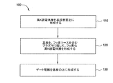
図1は、フッ素化高K誘電体層を基板表面に形成する方法100の一の実施形態のフローチャートである。図2A〜2Dを方法100に対応させて、トランジスタまたはキャパシタのような半導体素子に使用される誘電体材料を形成する様子を示している。工程110では、高K誘電体層202を基板201の上に形成する。工程120では、基板201を、フッ素ソースを含むプラズマに曝して、フッ素化高k誘電体層204を形成する。工程130では、ゲート電極206を基板201の上に形成する。
Exemplary Embodiment FIG. 1 is a flowchart of one embodiment of a
工程110の高K誘電体層202は基板の上に、原子層堆積法(ALD)、化学気相堆積法(CVD)、物理気相堆積法(PVD)、熱酸化法、及びプラズマ堆積法、及びこれらの方法の組み合わせのような従来の堆積法によって堆積させることができる。好適な実施形態では、高k誘電体層202をALDプロセス及び装置によって堆積させるが、このALDプロセス及び装置は、例えば2005年12月8日公開の「ハフニウム含有高K誘電体材料を原子層堆積させる装置及び方法」と題し、かつアプライドマテリアルズ社に譲渡される同時係属中の米国特許出願公開公報第2005/0271812号に記載されており、この特許文献を本明細書において参照することにより当該特許文献の内容が本明細書に組み込まれる。高k誘電体層202は普通、約10オングストローム〜約1000オングストローム、好ましくは約20オングストローム〜約500オングストローム、更に好ましくは約50オングストローム〜約200オングストローム、例えば約100オングストロームの膜厚に堆積させる。任意の予備クリーニング工程は、高k誘電体層202を基板201の上に堆積させる前に行なうことができる。高k材料を堆積するための適切なチャンバの例として、FLEXSTAR(登録商標)を挙げることができ、FLEXSTAR(登録商標)は、カリフォルニア州サンタクララ市に本拠を置くアプライドマテリアルズ社が市販している。
The high-
高k誘電体層202をフッ素化して、工程120のフッ素化高k誘電体層204を形成している間、基板に、F2、及びアルゴンのような不活性ガスプラズマを同時に流すことにより形成されるフッ素原子を衝突させる。F2の他に、他のフッ素含有ガスを使用して、NF3,HF,またはこれらの組み合わせのようなフッ素プラズマを形成することができる。使用することができる他の不活性ガスとして、ヘリウム、ネオン、及びキセノンを挙げることができる。窒素及び酸素のような他のガスを、不活性ガスの代わりに使用する、または不活性ガスと組み合わせて使用することができる。好適には、このプロセスに使用されるガスは炭素を含まない。一の実施形態では、フッ素化プロセスは、約10秒〜約360秒、好ましくは約30秒〜約180秒、例えば約120秒の時間に亘って行なわれる。フッ素化プロセスは普通、100℃未満、例えば約50℃〜100℃未満の温度で行なわれる。また、フッ素化プロセスは、約50ワット〜約2,500ワット、例えば約70ワット〜約200ワットのように、約50ワット〜約1,000ワットのプラズマ電力値、及び約10mTorr〜約100mTorrの圧力で行なわれる。フッ素は、約0.1slm〜約1.0slmの流量を有する。処理ガスの個々のガス流量及び合計ガス流量は、処理チャンバのサイズ、処理チャンバの温度、及び処理対象の基板のサイズのような多数の処理要素に従って変わり得る。好適な実施形態では、フッ素化プロセスにおいては、中密度の低イオンエネルギーフッ素プラズマを使用する。低イオンエネルギーパルス状フッ素含有プラズマによって、フッ素を高k誘電体ゲート積層構造に、十分大きいエネルギーをイオンエッチングに利用することなく、取り込むことができる。或る実施形態では、フッ素化誘電体層中のフッ素の濃度は、1E14原子/cm2〜4E15原子/cm2である。
Formed by simultaneously flowing an inert gas plasma such as F 2 and argon through the substrate while fluorinating the high-
別の実施形態では、プラズマフッ素化はチャンバ内で、約5〜20mTorrまたは約10〜20mTorrの範囲の圧力、200〜800ワット、例えば約250ワット〜約600ワットのプラズマ電力の条件で行なわれる。フッ素ガスはチャンバに、約100〜200sccmの範囲の流量で流し込むことができる。一の実施形態においては、プラズマフッ素化では、約10〜20MHzのパルス無線周波数プラズマプロセス、及び約5〜15kHzのパルスを使用する。プラズマフッ素化プロセスパラメータは、チャンバサイズ及び容積、更には誘電体膜の所望の厚さによって変わるように変化させることができる。任意のアニール工程は、プラズマフッ素化プロセスの前に、または後に行なうことができる。プラズマフッ素化プロセスパラメータは、誘電体をエッチングするために十分大きいエネルギーを利用することができなくても済むように選択される。 In another embodiment, plasma fluorination is performed in the chamber at a pressure in the range of about 5-20 mTorr or about 10-20 mTorr, plasma power of 200-800 Watts, such as about 250 Watts to about 600 Watts. Fluorine gas can be flowed into the chamber at a flow rate in the range of about 100-200 sccm. In one embodiment, plasma fluorination uses a pulsed radio frequency plasma process of about 10-20 MHz and a pulse of about 5-15 kHz. The plasma fluorination process parameters can be varied to vary with chamber size and volume, as well as the desired thickness of the dielectric film. An optional annealing step can be performed before or after the plasma fluorination process. The plasma fluorination process parameters are selected such that sufficient energy is not available to etch the dielectric.
工程130のゲート電極206は、基板201の上に、構造をプラズマに曝し、そしてアニールする前に堆積させることができ、ポリシリコン層、アモルファスシリコン層のようなゲート電極206、またはチタン、窒化チタン、タンタル、窒化タンタル、タングステン、窒化タングステン、及び他の高融点金属のような金属層、または他の適切な電極材料をフッ素化高k誘電体層204の上に堆積させることができる。
The
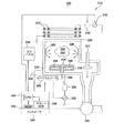
図3は、カリフォルニア州サンタクララ市に本拠を置くアプライドマテリアルズ社が製造するプラズマプロセス反応装置300の模式図である。プラズマプロセス反応装置は、本発明を実施するために使用することができる反応装置の一例である誘導プラズマソース反応装置である。
FIG. 3 is a schematic diagram of a
反応装置300は、静電チャック316を導電性ボディ(壁)330の内部に有するプロセスチャンバ310と、そしてコントローラ340と、を備える。チャンバ310には、ほぼ平坦な誘電性天井部320を設ける。チャンバ310の他の変形例は他のタイプの天井部、例えばドーム状天井部を有することができる。天井部320の上には、少なくとも一つの誘導コイル素子312(2つの同軸素子312が示される)が配置される。誘導コイル素子312は、第1整合回路319を介してプラズマ電源318に接続される。プラズマ電源318は通常、最大300Wの電力を、例えば50kHz〜13.56MHzの範囲の調整可能な周波数で生成することができる。
The
静電チャック316は、第1電極354と、そして誘電体材料に埋め込まれる第2電極356と、を含む。第1電極354及び第2電極356をDC電位でバイアスすることにより、基板314を保持する吸着作用を起こす。吸着電圧を静電チャック316、及びマスクから離間するウェハに印加することにより、電荷分布を基板314の下面に沿って、かつ静電チャック316の表面を覆うように発生させる。これらの電荷の極性を逆にすることにより、吸着静電力が基板314と静電チャック316との間に生じる。この力は基板314をチャック316の上に、処理チャンバ310内のプラズマを介在させることなく保持するので、基板314の導通接地経路が得られる。静電チャック316は単極チャックとすることもできる。
The
静電チャック316は、第2整合回路324を介してバイアス電源322に接続される。バイアス電源322は普通、50kHz〜13.56MHzの調整可能な周波数、及び0〜5000ワットの電力を有するRF信号を生成する機能を備える。任意であるが、バイアス電源322はDC電源またはパルスDC電源とすることができる。コントローラ340は、中央処理ユニット(CPU)344と、メモリ342と、そしてCPU344のサポート回路346と、を備え、そしてチャンバ310の、従って上に議論した窒化プロセスの構成要素に対する制御を容易にする。
The
別の実施形態では、静電チャック316を作動させる電圧は、別の「チャック」電源(図示せず)によって供給することができる。チャック電源の一方の出力端子はチャック電極に接続される。他方の出力端子は通常、電気接地に接続されるが、別の構成として、静電チャック316の金属ボディ部分に接続することができる。作動状態では、基板は誘電体材料と接触するように配置され、そして直流電圧を電極に印加して静電吸着力を、または静電吸着バイアスを生成することにより、基板を静電チャック316の上側表面に固着させる。
In another embodiment, the voltage that activates the
作動状態では、半導体ウェハ314を静電チャック316の上に載置し、そしてプロセスガスをガスパネル338から流入ポート326を通って供給してガス混合物350を生成する。ガス混合物350に点火して、プラズマ355をチャンバ310内に、電源をプラズマ電源318から印加することにより生成する。チャンバ310の内部の圧力は、スロットルバルブ327及び真空ポンプ336を使用して制御される。通常、チャンバ壁330は電気接地334に接続される。壁330の温度は、壁330を貫通して走る液体収容導管(図示せず)を使用して制御される。
In operation, the
基板314の温度は、静電チャック316の温度を安定させることにより制御される。一の実施形態では、ガス供給源348からのヘリウムガスは、ガス導管349を経由して、静電チャック316の表面に、基板314の裏面と静電チャック316の上側表面との間に形成される微小空間に達するように形成される流路(図示せず)に供給される。処理中、静電チャック316は、静電チャック316の台座の内部の抵抗加熱ヒータ(図示せず)によって定常温度にまで加熱することができ、そして次に、ヘリウムガスによって基板314に対する均一な加熱が容易になる。
The temperature of the
プロセスチャンバ310の制御を上に記載したように容易にするために、コントローラ340は、産業現場において使用することにより種々のチャンバ及びサブプロセッサを制御することができるいずれかの形態の汎用コンピュータプロセッサの内の一つの汎用コンピュータプロセッサとすることができる。CPU344のメモリ342またはコンピュータ読み取り可能な媒体は、ランダムアクセスメモリ(RAM)、リードオンリメモリ(ROM)、フロッピィディスク、ハードディスクのような容易に入手することができるメモリ、または他のいずれかの形態の自律動作型の、または遠隔操作型のデジタルストレージの内の一つ以上とすることができる。サポート回路346はCPU344に接続されてプロセッサを従来の態様でサポートする。これらの回路はキャッシュ、電源、クロック回路、入力/出力回路、及びサブシステムなどを含む。本発明による方法は一般的に、メモリ342にソフトウェアルーチンとして保存される。ソフトウェアルーチンは、CPU344によって制御されているハードウェアから遠く離れて位置する第2CPU(図示せず)によって保存する、そして/または実行することもできる。
To facilitate control of the
プラズマによる窒素ガスの分解過程が窒化に影響する現象を利用するプロセス反応装置300についての他の詳細は、アプライドマテリアルズ社に譲渡され、かつ米国特許第7,179754号として2004年12月2日に発行された「ゲート誘電体のプラズマ窒化を振幅変調無線周波数エネルギーを使用して行なう方法及び装置」と題する米国特許出願公開公報第2004/0242021号に記載されており、この特許文献の内容の内、本発明と矛盾することがない部分を本明細書において参照することにより、当該部分が本明細書に組み込まれる。適切なDPNチャンバの例として、カリフォルニア州サンタクララ市に本拠を置くアプライドマテリアルズ社が市販しているDPN CenturaTMを挙げることができる。他の適切なプラズマチャンバとして、アプライドマテリアルズ社が市販しているP3iチャンバを挙げることができる。
Other details of the
図4は、本発明の一の実施形態による方法400のフロー図である。任意であるが、基板の表面をクリーニングして基板の表面に形成されている可能性のある自然酸化膜を除去することができる。プロセスは、シリコン基板を第1処理チャンバに導入する工程402から始まる。約5オングストローム〜約100オングストロームの珪酸ハフニウム(HfSiOx)をシリコンウェハ上に工程404で成長させる。表面クリーニング及び高k誘電体層形成についての詳細は、アプライドマテリアルズ社に譲渡され、かつ2003年12月18日に発行された「高誘電率材料の核形成を促進する表面前処理」と題する米国特許出願公開公報第2003/0232501号に記載されており、この特許文献を本明細書において参照することにより、この特許文献の内容が本明細書に組み込まれる。珪酸ハフニウム層は、この方法を使用して堆積する材料の一例である。本発明は、4.0よりも大きい誘電率を有する高K誘電体材料とすることができる他の種類のゲート誘電体に適用することができる。
FIG. 4 is a flow diagram of a
任意であるが、基板は、カリフォルニア州サンタクララ市に本拠を置くアプライドマテリアルズ社が市販しているCENTURATM RADIANCETM高速熱処理(RTP)チャンバのようなアニールチャンバに搬送することにより、HfSiOx膜の堆積後アニールを行うことができる。堆積後アニールは、基板を約500℃〜約1200℃、好ましくは約550℃〜約700℃の温度で約30秒〜約90秒に亘ってアニールする、例えば650℃で約60秒に亘ってアニールすることにより行うことができる。一般的に、アニールチャンバ雰囲気は、O2,N2,NH3,N2H4,NO,N2O,またはこれらのガスの組み合わせのような少なくとも一つのアニールガスを含む。アニールチャンバは、約5Torr〜約100Torr、例えば約50Torrの圧力に維持される。 Optionally, the substrate is transferred to an annealing chamber such as a CENTURA ™ RADIANCE ™ Rapid Thermal Treatment (RTP) chamber marketed by Applied Materials, Inc., based in Santa Clara, Calif., To form an HfSiO x film. Annealing can be performed after deposition. The post-deposition anneal anneals the substrate at a temperature of about 500 ° C. to about 1200 ° C., preferably about 550 ° C. to about 700 ° C. for about 30 seconds to about 90 seconds, for example, at 650 ° C. for about 60 seconds. This can be done by annealing. Generally, the annealing chamber atmosphere includes at least one annealing gas, such as O 2 , N 2 , NH 3 , N 2 H 4 , NO, N 2 O, or a combination of these gases. The annealing chamber is maintained at a pressure of about 5 Torr to about 100 Torr, such as about 50 Torr.
工程406では、基板を次に、フッ素含有ガスを少なくとも含むプラズマチャンバに搬送する。好適な実施形態においては、フッ素化プロセスでは、中密度の低イオンエネルギーフッ素プラズマを使用する。低イオンエネルギーパルス状フッ素含有プラズマによって、フッ素を高kゲート積層構造に、イオンエッチング用の十分に大きいエネルギーを用いることなく取り込むことができる。フッ素化プロセスは、誘導パルスプラズマ、容量結合プラズマソース、または連続波誘導及び容量結合の混合プラズマソースを使用して行なうことができる。
In
任意であるが、基板をRTP処理チャンバに戻すように搬送し、このRTP処理チャンバでは、ポストフッ素化アニール工程が行なわれる。ポストフッ素化アニールを施している間、基板は約600℃〜約1200℃、好ましくは約700℃〜約1100℃の温度で、約1秒〜約120秒、好ましくは約30秒〜約90秒の時間に亘って、例えば約1000℃で約60秒に亘ってアニールされる。一般的に、アニールチャンバ雰囲気は、O2,N2,NH3,N2H4,NO,N2O,またはこれらのガスの組み合わせのような少なくとも一つのアニールガスを含む。アニールチャンバは、約5Torr〜約100Torr、例えば約15Torrの圧力に維持される。別の方法として、ポスト窒化アニールは2ステッププロセスにより行なわれ、2ステッププロセスでは、不活性化ステップまたは還元ステップの後に酸化ステップを行なう。 Optionally, the substrate is transferred back to the RTP processing chamber where a post fluorination annealing step is performed. During post-fluorination annealing, the substrate is at a temperature of about 600 ° C. to about 1200 ° C., preferably about 700 ° C. to about 1100 ° C., for about 1 second to about 120 seconds, preferably about 30 seconds to about 90 seconds. For example, at about 1000 ° C. for about 60 seconds. Generally, the annealing chamber atmosphere includes at least one annealing gas, such as O 2 , N 2 , NH 3 , N 2 H 4 , NO, N 2 O, or a combination of these gases. The annealing chamber is maintained at a pressure of about 5 Torr to about 100 Torr, such as about 15 Torr. Alternatively, the post nitridation anneal is performed by a two-step process, in which an oxidation step is performed after an inactivation step or a reduction step.
フッ素化された高k誘電体層を形成した後、ポリシリコンのようなゲート電極を、低圧化学気相堆積法(LPCVD)、原子層エピタキシー法(ALE)、熱分解法、またはこの技術分野で公知の他の方法により堆積させることができる。ポリシリコン層は一般的に、ボロン、リン、または砒素のようなドーパントを含む。ゲート電極は金属層とすることもできる。 After forming a fluorinated high-k dielectric layer, a gate electrode such as polysilicon can be formed by low pressure chemical vapor deposition (LPCVD), atomic layer epitaxy (ALE), pyrolysis, or in this technical field. It can be deposited by other known methods. The polysilicon layer typically includes a dopant such as boron, phosphorus, or arsenic. The gate electrode can also be a metal layer.
図5は、本明細書に開示されるプロセスを実施する機能を備える統合処理システム500の模式図である。統合処理システム500は、クリーニングモジュール510と、そして熱処理/堆積メインフレームシステム530と、を備える。図5に示すように、クリーニングモジュール510は、カリフォルニア州サンタクララ市に本拠を置くアプライドマテリアルズ社から入手することができるOASIS CLEANTMシステムである。熱処理/堆積メインフレームシステム530は、CENTURA(登録商標)システムであり、これもまたカリフォルニア州サンタクララ市に本拠を置くアプライドマテリアルズ社から市販されている。本明細書に開示されるプロセスを実行するシステムのこの特定の実施形態は、本発明を例示するために提供されるのであり、本発明の範囲を制限するために使用されるものとして捉えられるべきではない。
FIG. 5 is a schematic diagram of an
クリーニングモジュール510は一般的に、一つ以上の基板カセット512と、基板搬送領域内に配置される一つ以上の搬送ロボット514と、そして一つ以上の枚様式基板クリーニングチャンバ516と、を含む。枚様式基板クリーニングシステムの他の態様及び形態については、2002年3月14日に発行された「ウェハクリーニング方法及び装置」と題する米国特許出願公開公報第2002/0029788号、及び2002年5月30日に発行された「枚様式ウェハ処理装置のウェハスプレー構造」と題する米国特許出願公開公報第2002/0063169号に開示されており、これらの特許文献の両方の内容の内、本開示と矛盾することがない部分を本明細書において参照することにより、当該部分の全体が本明細書に組み込まれる。
The
熱処理/堆積メインフレームシステム530は一般的に、ロードロックチャンバ532と、搬送チャンバ534と、そして処理チャンバ536A,536B,536C,及び536Dと、を含む。搬送チャンバ534は好ましくは、1mTorr〜約100Torrの圧力であり、そして好ましくは、N2雰囲気のような不活性雰囲気を含む。ロードロックチャンバ532によって、搬送チャンバ534が低い圧力の非反応性環境になっている状態で、基板を熱処理/堆積メインフレームシステム530に搬入し、そして熱処理/堆積メインフレームシステム530から搬出することができる。搬送チャンバ534は一つ以上のブレードを有するロボット540を含み、これらのブレードによって基板をロードロックチャンバ532と処理チャンバ536A,536B,536C,及び536Dとの間で搬送する。処理チャンバ536A,536B,536C,または536Dの内のいずれかの処理チャンバを、熱処理/堆積メインフレームシステム530から、システム530によって行なわれることになる特定のプロセスに必要ではない場合に取り外すことができる。
The heat treatment /
任意の前処理工程、及び高K誘電体層形成をメインフレームシステムで行なって、高K誘電体層を形成する前に自然酸化膜の形成を抑制し、そして/または基板の前処理表面の汚染を低減すると有利であると考えられている。他の実施形態では、前処理工程では、研磨、エッチング、還元、酸化、水酸化、アニール、及び/又はベークを行なうことができる。基板を空気に前処理工程と高K誘電体層形成との間で曝すことにより、高K誘電体材料の基板上での核形成の効果を低減することができる。図5に示すように、クリーニングモジュール510をメインフレームシステム530に接続することにより、基板上での自然酸化膜の形成を更に抑制し、そして/またはクリーニング工程と他の処理工程との間での基板の汚染を更に低減することは任意である。勿論、他の実施形態では、クリーニング工程は、熱処理/堆積メインフレームシステムとは別のクリーニングモジュールにおいて行なうことができる。
Optional pre-treatment steps and high-K dielectric layer formation are performed in the mainframe system to suppress the formation of native oxide before forming the high-K dielectric layer and / or contamination of the pre-treatment surface of the substrate. It is considered advantageous to reduce. In other embodiments, the pretreatment step can be polishing, etching, reducing, oxidizing, hydroxylating, annealing, and / or baking. By exposing the substrate to air between the pretreatment step and the formation of the high K dielectric layer, the effect of nucleation on the substrate of the high K dielectric material can be reduced. As shown in FIG. 5, the
更に、ゲート電極、すなわち金属またはポリシリコンのいずれかを堆積させる前に、高kゲート積層構造をin−situでフッ素化する(その場でフッ素化する)ことにより、ゲート誘電体とゲート電極との間の界面での不所望の化学反応を防止することができると考えられる。ゲート電極を堆積させる前に高k材料の酸素空孔をパシベートすることにより、反応性の低い表面を、堆積金属または堆積ポリシリコンに持たせることができると考えられる。その結果、全ての工程、すなわち高k堆積工程、フッ素化を含むポスト堆積処理工程、及びゲート電極堆積工程を、大気に曝すことなく一つの装置内で一括して行なうプロセスは、一つの装置内で一括して行なわれることがない他のプロセスよりも優れていると考えられる。 Further, by depositing the high-k gate stack in-situ (in situ fluorination) prior to depositing either the gate electrode, ie metal or polysilicon, the gate dielectric and gate electrode It is believed that undesired chemical reactions at the interface between can be prevented. It is believed that the deposited metal or deposited polysilicon can have a less reactive surface by passivating high-k material oxygen vacancies prior to depositing the gate electrode. As a result, all the processes, that is, the high-k deposition process, the post-deposition treatment process including fluorination, and the gate electrode deposition process are performed in one apparatus without being exposed to the atmosphere. It is considered to be superior to other processes that are not performed in batch.
高K誘電体層を形成するように構成される統合処理システム500の一の実施形態は、フッ素化プロセスを上述したように行なうように適合させた処理チャンバ536Aと、ハフニウム含有層のような高誘電率材料を堆積させるように適合させた化学気相堆積チャンバまたは原子層堆積チャンバのような、或るプロセスを実施するように適合させた処理チャンバ536Bと、を備える。別の実施形態では、処理チャンバ536Cは、高速熱処理(RTP)チャンバを含み、高速熱処理(RTP)チャンバでは、構造をアニールすることができる。RTPチャンバは、アプライドマテリアルズ社から入手することができるXEチャンバ,XE Plusチャンバ、またはRadianceチャンバとすることができる。別の実施形態では、処理チャンバ536Dは、アプライドマテリアルズ社から入手することができ、かつゲート誘電体層を堆積するように適合させたPOLYgenのような低圧化学気相堆積チャンバ(LPCVD)を含む。システム500の他の実施形態は本発明の範囲に含まれる。例えば、システム上での特定の処理チャンバの位置は変更することができる、または処理チャンバの数は変更することができる。
One embodiment of an
図6は、プラズマチャンバ1の一の実施形態の等角断面図であり、プラズマチャンバ1は、プラズマ支援化学気相堆積(PECVD)プロセス、高密度プラズマ化学気相堆積(HDPCVD)プロセス、イオン注入プロセス、エッチングプロセス、及び他のプラズマプロセスを行なうように構成される。プラズマチャンバ1は、チャンバ1の本体3に接続されるトロイダルプラズマソース600を含む。本体3は、蓋部10及び底面15に接続される側壁5を含み、底面15によって内部容積20を区切っている。プラズマチャンバ1の他の例は、2002年6月5日に出願され、かつ2005年9月6日に発行された米国特許第6,939,434号、及び2004年2月24日に出願され、かつ2005年5月17日に発行された米国特許第6,893,907号に記載されており、これらの特許文献の両方を本明細書において参照することにより、これらの特許文献の内容全体が本明細書に組み込まれる。
FIG. 6 is an isometric cross-sectional view of one embodiment of a
内部容積20には、シャワーヘッド700と基板支持体800との間に形成される処理領域25が含まれる。ポンプ領域30が支持体800の一部を取り囲む。ポンプ領域30は、真空ポンプ40と、底面15に形成されるポート45に配置されるバルブ35を介して選択的に連通する。一の実施形態では、バルブ35はスロットルバルブであり、スロットルバルブは、内部容積20からポート45を介して真空ポンプ40に達するガスまたは蒸気の流れを制御する。一の実施形態では、バルブ35は、Oリングを使用することなく動作し、そして2005年4月26日に出願された米国特許出願公開公報第2006/0237136号に詳細に記載されており、この特許文献を本明細書において参照することにより、この特許文献の内容全体が本明細書に組み込まれる。
The
トロイダルプラズマソース600は、ほぼ「U」字形の第1導管650Aと、そしてほぼ「M」字形の第2導管650Bを含む。第1導管650A及び第2導管650Bはそれぞれ、少なくとも一つのアンテナ670A,670Bを含み、これらのアンテナを使用して誘導結合プラズマを、導管650A,650Bの各導管の内部領域655A,655Bの内部にそれぞれ形成する。各アンテナ670A,670Bは、RF電源671A,672Aのような電源に接続される巻き線またはコイルとすることができる。RFインピーダンス整合システム671B,672Bは各アンテナ670A,670Bに接続することもできる。ヘリウム、アルゴン、及び他のガスのようなプロセスガスは、導管650A,650Bの各導管の内部領域655A,655Bにそれぞれ供給することができる。一の実施形態では、プロセスガスは、各導管650A,650Bの内部領域655A,655Bに供給されるドーパント含有ガスを含むことができる。一の実施形態では、プロセスガスはガスソース630Aから供給され、ガスソース630Aは、チャンバ1の本体3に形成されるポート55に接続される。
一の実施形態では、導管650A,650Bの各対向端部は、チャンバ1の蓋部10に形成される該当するポート(導管650Bに対応するポート50A及び50Bがこの図において示される)に接続される。処理中、プロセスガスは、導管650A,650Bの各導管の内部領域655A,655Bに供給され、そしてRFパワーが各アンテナ670A,670Bに印加されて、ポート群、例えば50A〜50B、及び処理領域25を通過する循環プラズマ経路が形成される。詳細には、図6では、循環プラズマ経路は、ポート50Aを通ってポート50Bに、または逆にポート50Bを通ってポート50Aに、ガス供給アセンブリ700と基板支持体800との間の処理領域25を通過するようにして達することができる。各導管650A,650Bは、導管及びポート、例えば50A〜50Bの該当する端部の間に接続されるプラズマ流動手段606を含み、プラズマ流動手段606は、導管650A,650Bの各導管の内部に形成されるプラズマ経路を分岐させ、そして広くするように構成される。
In one embodiment, each opposing end of
ガス供給プレート700またはシャワーヘッドは、プレナム730を蓋部10と穿孔プレート720との間に画定する環状壁710を含む。穿孔プレート720は、プレートを貫通するように対称パターンに、または非対称パターンに形成される複数の孔を含む。ドーパント含有ガスのようなプロセスガスはプレナム730にポート55から供給することができる。一般的に、ドーパント含有ガスは、ボロン(シリコン内のp型不純物)またはリン(シリコン内のn型不純物)のようなドーパント不純物原子、及びフッ素及び/又は水素のような揮発性化学種から成る化学物質である。従って、ボロン、リン、または砒素、アンチモンなどのような他のドーパント化学種のフッ素化物及び/又は水素化物はドーパントガスとすることができる。例えば、ボロンドーパントが使用される場合、ドーパント含有ガスは、三フッ化ホウ素(BF3)またはジボラン(B2H6)を含むことができる。ガスは孔を通り抜け、そして穿孔プレート720下方の処理領域25に達するように流れることができる。一の実施形態では、穿孔プレート720はRFバイアスされて、処理領域25内でのプラズマの生成、及び/又は維持を容易にする。
The
基板支持体800は一般的に、上側層または水平円盤810と、そしてカソードアセンブリ820と、を含む。水平円盤810は、平滑な基板支持表面と、そして埋め込み電極815と、を含み、埋め込み電極815は、DC電源806を使用してバイアスすることにより基板と、水平円盤810の基板支持表面との間の静電吸着力を強めることができる。埋め込み電極815は、RFエネルギーを処理領域25に供給し、そしてRFバイアスを処理中に形成する電極として使用することもできる。埋め込み電極815は、RF電源805Aに接続することができ、そしてインピーダンス整合部805Bを含むこともできる。一の実施形態では、基板支持体800は、基板接触式冷却静電チャックであり、このチャックでは、チャックの内、基板と接触する部分が冷却される。冷却は、カソードアセンブリ820内に配置されて冷却剤を流路内で循環させる冷却剤流路(図示せず)によって行なわれる。
基板支持体800はリフトピンアセンブリ900を含むこともでき、リフトピンアセンブリ900は複数のリフトピン910を含む(この図には、一つしか示していない)。これらのリフトピン910によって、一つ以上の基板の搬送が、基板を水平円盤810の上方に選択的に持ち上げ、そして水平円盤810の上方で支持することにより容易になり、そしてこれらのリフトピン910を離間させることにより、ロボットブレード(図示せず)をこれらのリフトピンの間に位置させることができる。リフトピンアセンブリ900は、ピンブッシング920を含み、これらのピンブッシング920は水平円盤810及びカソードアセンブリ820の内の一方、または両方に接続される。
The
上述の実施形態について図4,5,及び6を参照しながら記載しているが、他の統合処理システム及びチャンバの組み合わせを、本明細書に記載される実施形態に使用することができることを理解されたい。更に、どのような数の処理チャンバも、統合システム以外の統合システムの一部とすることができる。 Although the above-described embodiments have been described with reference to FIGS. 4, 5, and 6, it is understood that other integrated processing system and chamber combinations can be used in the embodiments described herein. I want to be. Further, any number of processing chambers can be part of an integrated system other than the integrated system.
これまでの記述は、本発明の実施形態に関して行なわれているが、本発明の他の実施形態及び別の実施形態を、本発明の基本的範囲から逸脱しない範囲で想到することができ、そして本発明の範囲は以下に示す請求項によって規定される。 While the foregoing has been described with reference to embodiments of the present invention, other and alternative embodiments of the invention can be devised without departing from the basic scope thereof. The scope of the invention is defined by the claims that follow.
Claims (15)
基板を第1処理チャンバに導入する工程と、
所望の厚さを有する高k誘電体層を前記第1処理チャンバ内の前記基板の表面に形成する工程と、
前記基板を周囲空気に曝すことなく、第2処理チャンバに移す工程と、
前記基板を、前記第2処理チャンバ内に生成された、フッ素ソースガスを含む低エネルギープラズマに曝して、フッ素化された高k誘電体層を前記基板の上に、前記第2処理チャンバ内の高k誘電体層をエッチングすることなく形成する工程と、
前記基板を周囲空気に曝すことなく、第3処理チャンバに移す工程と、
ゲート電極を前記第3処理チャンバ内のフッ素化された高k誘電体層の上に形成する工程と、を含む、方法。 A method of forming a semiconductor device comprising:
Introducing the substrate into the first processing chamber;
Forming a high-k dielectric layer having a desired thickness on a surface of the substrate in the first processing chamber;
Transferring the substrate to a second processing chamber without exposing it to ambient air;
The substrate is exposed to a low energy plasma generated in the second processing chamber and containing a fluorine source gas, and a fluorinated high-k dielectric layer is placed on the substrate and in the second processing chamber. Forming a high-k dielectric layer without etching;
Transferring the substrate to a third processing chamber without exposing it to ambient air;
Forming a gate electrode on the fluorinated high-k dielectric layer in the third processing chamber.
高k誘電体層を基板の上に形成する工程と、
前記高k誘電体層をアニールする工程と、
前記基板を、処理チャンバ内に生成された、低イオンエネルギーフッ素含有プラズマに曝して、フッ素化された高k誘電体層を形成して、高kゲート積層構造中の酸素空孔及び他の結合欠陥をパシベートする工程と、
前記フッ素化された高k誘電体層をアニールする工程と、
ゲート電極を前記フッ素化された高k誘電体層の上に形成する工程と、を含む、方法。 A method of forming a high-k gate stack structure comprising:
Forming a high-k dielectric layer on the substrate;
Annealing the high-k dielectric layer;
The substrate is exposed to a low ion energy fluorine-containing plasma generated in a processing chamber to form a fluorinated high-k dielectric layer to form oxygen vacancies and other bonds in the high-k gate stack. A passivating defect;
Annealing the fluorinated high-k dielectric layer;
Forming a gate electrode on the fluorinated high- k dielectric layer.
Applications Claiming Priority (3)
| Application Number | Priority Date | Filing Date | Title |
|---|---|---|---|
| US82702306P | 2006-09-26 | 2006-09-26 | |
| US60/827,023 | 2006-09-26 | ||
| PCT/US2007/079544 WO2008039845A2 (en) | 2006-09-26 | 2007-09-26 | Fluorine plasma treatment of high-k gate stack for defect passivation |
Publications (3)
| Publication Number | Publication Date |
|---|---|
| JP2010505281A JP2010505281A (en) | 2010-02-18 |
| JP2010505281A5 JP2010505281A5 (en) | 2010-11-11 |
| JP5590886B2 true JP5590886B2 (en) | 2014-09-17 |
Family
ID=39230940
Family Applications (1)
| Application Number | Title | Priority Date | Filing Date |
|---|---|---|---|
| JP2009530575A Active JP5590886B2 (en) | 2006-09-26 | 2007-09-26 | Fluorine plasma treatment for high-K gate stacks for defect passivation |
Country Status (4)
| Country | Link |
|---|---|
| US (1) | US7902018B2 (en) |
| JP (1) | JP5590886B2 (en) |
| TW (1) | TWI435376B (en) |
| WO (1) | WO2008039845A2 (en) |
Families Citing this family (31)
| Publication number | Priority date | Publication date | Assignee | Title |
|---|---|---|---|---|
| KR100788361B1 (en) * | 2006-12-12 | 2008-01-02 | 동부일렉트로닉스 주식회사 | Method of forming mosfet device |
| KR100877100B1 (en) * | 2007-04-16 | 2009-01-09 | 주식회사 하이닉스반도체 | Methods for manufacturing non-volatile memory device |
| JP2010199294A (en) * | 2009-02-25 | 2010-09-09 | Toshiba Corp | Semiconductor device |
| US9685186B2 (en) * | 2009-02-27 | 2017-06-20 | Applied Materials, Inc. | HDD pattern implant system |
| US9048186B2 (en) * | 2009-10-08 | 2015-06-02 | Taiwan Semiconductor Manufacturing Company, Ltd. | Methods for forming integrated circuits |
| WO2012083220A2 (en) * | 2010-12-16 | 2012-06-21 | The Regents Of The University Of California | Generation of highly n-type, defect passivated transition metal oxides using plasma fluorine insertion |
| US8802545B2 (en) * | 2011-03-14 | 2014-08-12 | Plasma-Therm Llc | Method and apparatus for plasma dicing a semi-conductor wafer |
| US8952458B2 (en) * | 2011-04-14 | 2015-02-10 | Taiwan Semiconductor Manufacturing Company, Ltd. | Gate dielectric layer having interfacial layer and high-K dielectric over the interfacial layer |
| US9006092B2 (en) * | 2011-11-03 | 2015-04-14 | United Microelectronics Corp. | Semiconductor structure having fluoride metal layer and process thereof |
| CN107611258A (en) | 2011-11-23 | 2018-01-19 | 应用材料公司 | Method for silica chemistry vapour deposition photoresist planarization |
| EP2806982B1 (en) * | 2012-01-27 | 2020-03-11 | Koninklijke Philips N.V. | Capacitive micro-machined transducer and method of manufacturing the same |
| WO2013146632A1 (en) * | 2012-03-28 | 2013-10-03 | 株式会社日立国際電気 | Semiconductor device manufacturing method, substrate processing method, substrate processing apparatus, and program |
| US8658490B2 (en) | 2012-04-04 | 2014-02-25 | Globalfoundries Inc. | Passivating point defects in high-K gate dielectric layers during gate stack formation |
| US8735305B2 (en) | 2012-05-24 | 2014-05-27 | Intermolecular, Inc. | Methods of forming fluorinated hafnium oxide gate dielectrics by atomic layer deposition |
| US8791003B2 (en) * | 2012-06-21 | 2014-07-29 | GlobalFoundries, Inc. | Methods for fabricating integrated circuits with fluorine passivation |
| KR20140032716A (en) | 2012-09-07 | 2014-03-17 | 삼성전자주식회사 | Semiconductor device and method for fabricating thereof |
| JP6329157B2 (en) * | 2012-10-12 | 2018-05-23 | ローレンス リバモア ナショナル セキュリティー, エルエルシー | Optical substrate flattening |
| US8821985B2 (en) | 2012-11-02 | 2014-09-02 | Intermolecular, Inc. | Method and apparatus for high-K gate performance improvement and combinatorial processing |
| US8981466B2 (en) * | 2013-03-11 | 2015-03-17 | International Business Machines Corporation | Multilayer dielectric structures for semiconductor nano-devices |
| CN103295890B (en) * | 2013-05-30 | 2015-12-09 | 北京大学 | Be deposited on the processing method of the gate medium on germanium base or three or five compounds of group base substrates |
| US8945414B1 (en) | 2013-11-13 | 2015-02-03 | Intermolecular, Inc. | Oxide removal by remote plasma treatment with fluorine and oxygen radicals |
| US9245793B2 (en) * | 2013-12-19 | 2016-01-26 | Intermolecular, Inc. | Plasma treatment of low-K surface to improve barrier deposition |
| US10134878B2 (en) * | 2016-01-14 | 2018-11-20 | Applied Materials, Inc. | Oxygen vacancy of IGZO passivation by fluorine treatment |
| US10580643B2 (en) * | 2016-02-16 | 2020-03-03 | Applied Materials, Inc. | Fluorination during ALD high-k, fluorination post high-k and use of a post fluorination anneal to engineer fluorine bonding and incorporation |
| CN109075207B (en) | 2016-07-19 | 2023-08-11 | 应用材料公司 | High-k dielectric materials comprising zirconia for use in display devices |
| US20180033619A1 (en) * | 2016-07-29 | 2018-02-01 | Applied Materials, Inc. | Performing decoupled plasma fluorination to reduce interfacial defects in film stack |
| US10134873B2 (en) * | 2016-11-18 | 2018-11-20 | Taiwan Semiconductor Manufacturing Co., Ltd. | Semiconductor device gate structure and method of fabricating thereof |
| US10431462B2 (en) * | 2017-02-15 | 2019-10-01 | Lam Research Corporation | Plasma assisted doping on germanium |
| US10629749B2 (en) | 2017-11-30 | 2020-04-21 | Taiwan Semiconductor Manufacturing Co., Ltd. | Method of treating interfacial layer on silicon germanium |
| US11501972B2 (en) * | 2020-07-22 | 2022-11-15 | Applied Materials, Inc. | Sacrificial capping layer for passivation using plasma-based implant process |
| US20230317634A1 (en) * | 2022-04-05 | 2023-10-05 | Applied Materials, Inc. | Coatings with diffusion barriers for corrosion and contamination protection |
Family Cites Families (269)
| Publication number | Priority date | Publication date | Assignee | Title |
|---|---|---|---|---|
| US3594295A (en) | 1966-09-19 | 1971-07-20 | Physics Technology Lab Inc | Rf sputtering of insulator materials |
| US3427514A (en) * | 1966-10-13 | 1969-02-11 | Rca Corp | Mos tetrode |
| FR2134290B1 (en) | 1971-04-30 | 1977-03-18 | Texas Instruments France | |
| US4096509A (en) | 1976-07-22 | 1978-06-20 | The United States Of America As Represented By The Secretary Of The Air Force | MNOS memory transistor having a redeposited silicon nitride gate dielectric |
| DE2967538D1 (en) | 1978-06-14 | 1985-12-05 | Fujitsu Ltd | Process for producing a semiconductor device having an insulating layer of silicon dioxide covered by a film of silicon oxynitride |
| US4335391A (en) | 1978-12-11 | 1982-06-15 | Texas Instruments Incorporated | Non-volatile semiconductor memory elements and methods of making |
| US4262631A (en) * | 1979-10-01 | 1981-04-21 | Kubacki Ronald M | Thin film deposition apparatus using an RF glow discharge |
| US4310380A (en) * | 1980-04-07 | 1982-01-12 | Bell Telephone Laboratories, Incorporated | Plasma etching of silicon |
| JPS56158873A (en) | 1980-05-14 | 1981-12-07 | Hitachi Ltd | Dry etching method |
| JPS57113264A (en) | 1980-12-29 | 1982-07-14 | Fujitsu Ltd | Manufacture of mis type capacitor |
| US4459739A (en) | 1981-05-26 | 1984-07-17 | Northern Telecom Limited | Thin film transistors |
| DE3279239D1 (en) | 1981-07-27 | 1988-12-29 | Toshiba Kk | Thin-film transistor and method of manufacture therefor |
| JPS5861763A (en) * | 1981-10-09 | 1983-04-12 | 武笠 均 | Feel sensor fire fighting apparatus |
| US4439463A (en) * | 1982-02-18 | 1984-03-27 | Atlantic Richfield Company | Plasma assisted deposition system |
| US4605947A (en) | 1983-03-07 | 1986-08-12 | Motorola Inc. | Titanium nitride MOS device gate electrode and method of producing |
| US4545112A (en) | 1983-08-15 | 1985-10-08 | Alphasil Incorporated | Method of manufacturing thin film transistors and transistors made thereby |
| US4651185A (en) * | 1983-08-15 | 1987-03-17 | Alphasil, Inc. | Method of manufacturing thin film transistors and transistors made thereby |
| JPS60114570A (en) | 1983-11-25 | 1985-06-21 | Canon Inc | Evacuating system for plasma cvd device |
| US4534826A (en) | 1983-12-29 | 1985-08-13 | Ibm Corporation | Trench etch process for dielectric isolation |
| US6784033B1 (en) | 1984-02-15 | 2004-08-31 | Semiconductor Energy Laboratory Co., Ltd. | Method for the manufacture of an insulated gate field effect semiconductor device |
| US4563367A (en) * | 1984-05-29 | 1986-01-07 | Applied Materials, Inc. | Apparatus and method for high rate deposition and etching |
| US4585516A (en) * | 1985-03-04 | 1986-04-29 | Tegal Corporation | Variable duty cycle, multiple frequency, plasma reactor |
| JPH0746729B2 (en) | 1985-12-26 | 1995-05-17 | キヤノン株式会社 | Method of manufacturing thin film transistor |
| US4745082A (en) | 1986-06-12 | 1988-05-17 | Ford Microelectronics, Inc. | Method of making a self-aligned MESFET using a substitutional gate with side walls |
| US4725560A (en) * | 1986-09-08 | 1988-02-16 | International Business Machines Corp. | Silicon oxynitride storage node dielectric |
| US5000113A (en) * | 1986-12-19 | 1991-03-19 | Applied Materials, Inc. | Thermal CVD/PECVD reactor and use for thermal chemical vapor deposition of silicon dioxide and in-situ multi-step planarized process |
| US4913929A (en) * | 1987-04-21 | 1990-04-03 | The Board Of Trustees Of The Leland Stanford Junior University | Thermal/microwave remote plasma multiprocessing reactor and method of use |
| JP2664685B2 (en) | 1987-07-31 | 1997-10-15 | 株式会社東芝 | Method for manufacturing semiconductor device |
| US4851370A (en) | 1987-12-28 | 1989-07-25 | American Telephone And Telegraph Company, At&T Bell Laboratories | Fabricating a semiconductor device with low defect density oxide |
| US5874766A (en) * | 1988-12-20 | 1999-02-23 | Matsushita Electric Industrial Co., Ltd. | Semiconductor device having an oxynitride film |
| JPH02230736A (en) * | 1989-03-03 | 1990-09-13 | Seiko Epson Corp | Formation and treatment of dielectric film |
| US4948458A (en) | 1989-08-14 | 1990-08-14 | Lam Research Corporation | Method and apparatus for producing magnetically-coupled planar plasma |
| US5292673A (en) * | 1989-08-16 | 1994-03-08 | Hitachi, Ltd | Method of manufacturing a semiconductor device |
| KR910010516A (en) * | 1989-11-15 | 1991-06-29 | 아오이 죠이치 | Semiconductor memory device |
| US5173442A (en) | 1990-07-23 | 1992-12-22 | Microelectronics And Computer Technology Corporation | Methods of forming channels and vias in insulating layers |
| US5228950A (en) | 1990-12-04 | 1993-07-20 | Applied Materials, Inc. | Dry process for removal of undesirable oxide and/or silicon residues from semiconductor wafer after processing |
| US5314724A (en) | 1991-01-08 | 1994-05-24 | Fujitsu Limited | Process for forming silicon oxide film |
| US5391510A (en) * | 1992-02-28 | 1995-02-21 | International Business Machines Corporation | Formation of self-aligned metal gate FETs using a benignant removable gate material during high temperature steps |
| US5726087A (en) * | 1992-04-30 | 1998-03-10 | Motorola, Inc. | Method of formation of semiconductor gate dielectric |
| JP2662365B2 (en) | 1993-01-28 | 1997-10-08 | アプライド マテリアルズ インコーポレイテッド | Single-substrate vacuum processing apparatus with improved discharge system |
| US5335138A (en) | 1993-02-12 | 1994-08-02 | Micron Semiconductor, Inc. | High dielectric constant capacitor and method of manufacture |
| DE69405438T2 (en) | 1993-03-24 | 1998-04-02 | At & T Corp | Process for the formation of dielectric oxynitride layers in the production of integrated circuits |
| KR100324792B1 (en) | 1993-03-31 | 2002-06-20 | 히가시 데쓰로 | Plasma processing apparatus |
| US5865896A (en) * | 1993-08-27 | 1999-02-02 | Applied Materials, Inc. | High density plasma CVD reactor with combined inductive and capacitive coupling |
| KR100291971B1 (en) | 1993-10-26 | 2001-10-24 | 야마자끼 순페이 | Substrate processing apparatus and method and thin film semiconductor device manufacturing method |
| US5851602A (en) * | 1993-12-09 | 1998-12-22 | Applied Materials, Inc. | Deposition of high quality conformal silicon oxide thin films for the manufacture of thin film transistors |
| DE69433836D1 (en) | 1993-12-28 | 2004-07-15 | Applied Materials Inc | Process for plasma-assisted chemical vapor deposition of silicon oxynitride layers |
| JP2901493B2 (en) * | 1994-06-27 | 1999-06-07 | 日本電気株式会社 | Semiconductor memory device and method of manufacturing the same |
| US6251758B1 (en) | 1994-11-14 | 2001-06-26 | Applied Materials, Inc. | Construction of a film on a semiconductor wafer |
| US5609927A (en) * | 1995-06-06 | 1997-03-11 | Texas Instruments Incorporated | Processing methods for high-dielectric-constant materials |
| JP3514912B2 (en) | 1995-08-31 | 2004-04-05 | 東芝電子エンジニアリング株式会社 | Method for manufacturing thin film transistor |
| JPH09153616A (en) | 1995-09-28 | 1997-06-10 | Toshiba Corp | Semiconductor device and manufacture thereof |
| JP3522917B2 (en) * | 1995-10-03 | 2004-04-26 | 株式会社東芝 | Semiconductor device manufacturing method and semiconductor manufacturing apparatus |
| US6264812B1 (en) | 1995-11-15 | 2001-07-24 | Applied Materials, Inc. | Method and apparatus for generating a plasma |
| US6054013A (en) * | 1996-02-02 | 2000-04-25 | Applied Materials, Inc. | Parallel plate electrode plasma reactor having an inductive antenna and adjustable radial distribution of plasma ion density |
| US5872052A (en) | 1996-02-12 | 1999-02-16 | Micron Technology, Inc. | Planarization using plasma oxidized amorphous silicon |
| US5976993A (en) | 1996-03-28 | 1999-11-02 | Applied Materials, Inc. | Method for reducing the intrinsic stress of high density plasma films |
| US6254746B1 (en) | 1996-05-09 | 2001-07-03 | Applied Materials, Inc. | Recessed coil for generating a plasma |
| US6136654A (en) | 1996-06-07 | 2000-10-24 | Texas Instruments Incorporated | Method of forming thin silicon nitride or silicon oxynitride gate dielectrics |
| US6342277B1 (en) | 1996-08-16 | 2002-01-29 | Licensee For Microelectronics: Asm America, Inc. | Sequential chemical vapor deposition |
| JP3220394B2 (en) | 1996-09-27 | 2001-10-22 | 東京エレクトロン株式会社 | Plasma processing equipment |
| US6190513B1 (en) * | 1997-05-14 | 2001-02-20 | Applied Materials, Inc. | Darkspace shield for improved RF transmission in inductively coupled plasma sources for sputter deposition |
| JPH10150025A (en) | 1996-11-20 | 1998-06-02 | Mitsubishi Electric Corp | Plasma reactor |
| EP0847079A3 (en) | 1996-12-05 | 1999-11-03 | Texas Instruments Incorporated | Method of manufacturing an MIS electrode |
| JPH10173490A (en) * | 1996-12-10 | 1998-06-26 | Sony Corp | Synthesizer receiver |
| US5891798A (en) * | 1996-12-20 | 1999-04-06 | Intel Corporation | Method for forming a High dielectric constant insulator in the fabrication of an integrated circuit |
| US6320238B1 (en) | 1996-12-23 | 2001-11-20 | Agere Systems Guardian Corp. | Gate structure for integrated circuit fabrication |
| KR19980071011A (en) | 1997-01-24 | 1998-10-26 | 조셉 제이. 스위니 | High Temperature and High Flow Rate Chemical Vapor Deposition Apparatus and Related Deposition Methods |
| US5763922A (en) | 1997-02-28 | 1998-06-09 | Intel Corporation | CMOS integrated circuit having PMOS and NMOS devices with different gate dielectric layers |
| JP4355036B2 (en) * | 1997-03-18 | 2009-10-28 | キヤノンアネルバ株式会社 | Ionization sputtering equipment |
| US6551665B1 (en) | 1997-04-17 | 2003-04-22 | Micron Technology, Inc. | Method for improving thickness uniformity of deposited ozone-TEOS silicate glass layers |
| JP3221602B2 (en) * | 1997-05-21 | 2001-10-22 | セントラル硝子株式会社 | Method for forming nitrided oxide film |
| JP4344019B2 (en) | 1997-05-28 | 2009-10-14 | キヤノンアネルバ株式会社 | Ionized sputtering method |
| JPH111770A (en) | 1997-06-06 | 1999-01-06 | Anelva Corp | Sputtering apparatus and sputtering method |
| JP3191728B2 (en) * | 1997-06-23 | 2001-07-23 | 日本電気株式会社 | Semiconductor device and manufacturing method thereof |
| US6841439B1 (en) * | 1997-07-24 | 2005-01-11 | Texas Instruments Incorporated | High permittivity silicate gate dielectric |
| US6013553A (en) * | 1997-07-24 | 2000-01-11 | Texas Instruments Incorporated | Zirconium and/or hafnium oxynitride gate dielectric |
| US6020024A (en) * | 1997-08-04 | 2000-02-01 | Motorola, Inc. | Method for forming high dielectric constant metal oxides |
| US6345588B1 (en) * | 1997-08-07 | 2002-02-12 | Applied Materials, Inc. | Use of variable RF generator to control coil voltage distribution |
| US5960270A (en) | 1997-08-11 | 1999-09-28 | Motorola, Inc. | Method for forming an MOS transistor having a metallic gate electrode that is formed after the formation of self-aligned source and drain regions |
| US6352594B2 (en) * | 1997-08-11 | 2002-03-05 | Torrex | Method and apparatus for improved chemical vapor deposition processes using tunable temperature controlled gas injectors |
| US6287635B1 (en) | 1997-08-11 | 2001-09-11 | Torrex Equipment Corp. | High rate silicon deposition method at low pressures |
| US5834353A (en) * | 1997-10-20 | 1998-11-10 | Texas Instruments-Acer Incorporated | Method of making deep sub-micron meter MOSFET with a high permitivity gate dielectric |
| US5937303A (en) | 1997-10-29 | 1999-08-10 | Advanced Micro Devices | High dielectric constant gate dielectric integrated with nitrogenated gate electrode |
| US6041734A (en) * | 1997-12-01 | 2000-03-28 | Applied Materials, Inc. | Use of an asymmetric waveform to control ion bombardment during substrate processing |
| US6043157A (en) * | 1997-12-18 | 2000-03-28 | Advanced Micro Devices | Semiconductor device having dual gate electrode material and process of fabrication thereof |
| US6258675B1 (en) | 1997-12-18 | 2001-07-10 | Advanced Micro Devices, Inc. | High K gate electrode |
| US6083836A (en) | 1997-12-23 | 2000-07-04 | Texas Instruments Incorporated | Transistors with substitutionally formed gate structures and method |
| US6235650B1 (en) | 1997-12-29 | 2001-05-22 | Vanguard International Semiconductor Corporation | Method for improved semiconductor device reliability |
| US6140024A (en) | 1997-12-31 | 2000-10-31 | Texas Instruments Incorporated | Remote plasma nitridation for contact etch stop |
| EP0933814A1 (en) | 1998-01-28 | 1999-08-04 | Interuniversitair Micro-Elektronica Centrum Vzw | A metallization structure on a fluorine-containing dielectric and a method for fabrication thereof |
| US6294219B1 (en) | 1998-03-03 | 2001-09-25 | Applied Komatsu Technology, Inc. | Method of annealing large area glass substrates |
| US6506287B1 (en) * | 1998-03-16 | 2003-01-14 | Applied Materials, Inc. | Overlap design of one-turn coil |
| US6090653A (en) | 1998-03-30 | 2000-07-18 | Texas Instruments | Method of manufacturing CMOS transistors |
| US6254738B1 (en) | 1998-03-31 | 2001-07-03 | Applied Materials, Inc. | Use of variable impedance having rotating core to control coil sputter distribution |
| US6130123A (en) | 1998-06-30 | 2000-10-10 | Intel Corporation | Method for making a complementary metal gate electrode technology |
| US6027961A (en) * | 1998-06-30 | 2000-02-22 | Motorola, Inc. | CMOS semiconductor devices and method of formation |
| US6660134B1 (en) | 1998-07-10 | 2003-12-09 | Applied Materials, Inc. | Feedthrough overlap coil |
| US6049114A (en) * | 1998-07-20 | 2000-04-11 | Motorola, Inc. | Semiconductor device having a metal containing layer overlying a gate dielectric |
| US6358810B1 (en) * | 1998-07-28 | 2002-03-19 | Applied Materials, Inc. | Method for superior step coverage and interface control for high K dielectric capacitors and related electrodes |
| US6008095A (en) | 1998-08-07 | 1999-12-28 | Advanced Micro Devices, Inc. | Process for formation of isolation trenches with high-K gate dielectrics |
| US6140688A (en) | 1998-09-21 | 2000-10-31 | Advanced Micro Devices Inc. | Semiconductor device with self-aligned metal-containing gate |
| US6066533A (en) | 1998-09-29 | 2000-05-23 | Advanced Micro Devices, Inc. | MOS transistor with dual metal gate structure |
| US6255231B1 (en) | 1998-10-02 | 2001-07-03 | Taiwan Semiconductor Manufacturing Co., Ltd | Method for forming a gate oxide layer |
| US6117279A (en) | 1998-11-12 | 2000-09-12 | Tokyo Electron Limited | Method and apparatus for increasing the metal ion fraction in ionized physical vapor deposition |
| US6528856B1 (en) * | 1998-12-15 | 2003-03-04 | Intel Corporation | High dielectric constant metal oxide gate dielectrics |
| US6497796B1 (en) | 1999-01-05 | 2002-12-24 | Novellus Systems, Inc. | Apparatus and method for controlling plasma uniformity across a substrate |
| US6291282B1 (en) | 1999-02-26 | 2001-09-18 | Texas Instruments Incorporated | Method of forming dual metal gate structures or CMOS devices |
| US6436801B1 (en) | 1999-02-26 | 2002-08-20 | Texas Instruments Incorporated | Hafnium nitride gate dielectric |
| KR100745495B1 (en) | 1999-03-10 | 2007-08-03 | 동경 엘렉트론 주식회사 | Semiconductor fabrication method and semiconductor fabrication equipment |
| US6200893B1 (en) * | 1999-03-11 | 2001-03-13 | Genus, Inc | Radical-assisted sequential CVD |
| US6171900B1 (en) * | 1999-04-15 | 2001-01-09 | Taiwan Semiconductor Manufacturing Company | CVD Ta2O5/oxynitride stacked gate insulator with TiN gate electrode for sub-quarter micron MOSFET |
| US6255698B1 (en) | 1999-04-28 | 2001-07-03 | Advanced Micro Devices, Inc. | Separately optimized gate structures for n-channel and p-channel transistors in an integrated circuit |
| JP2000331993A (en) | 1999-05-19 | 2000-11-30 | Mitsubishi Electric Corp | Plasma processing device |
| US6355108B1 (en) * | 1999-06-22 | 2002-03-12 | Applied Komatsu Technology, Inc. | Film deposition using a finger type shadow frame |
| US6376807B1 (en) * | 1999-07-09 | 2002-04-23 | Applied Materials, Inc. | Enhanced cooling IMP coil support |
| US6060755A (en) | 1999-07-19 | 2000-05-09 | Sharp Laboratories Of America, Inc. | Aluminum-doped zirconium dielectric film transistor structure and deposition method for same |
| US6297539B1 (en) | 1999-07-19 | 2001-10-02 | Sharp Laboratories Of America, Inc. | Doped zirconia, or zirconia-like, dielectric film transistor structure and deposition method for same |
| US6171910B1 (en) * | 1999-07-21 | 2001-01-09 | Motorola Inc. | Method for forming a semiconductor device |
| US6063704A (en) | 1999-08-02 | 2000-05-16 | National Semiconductor Corporation | Process for incorporating silicon oxynitride DARC layer into formation of silicide polysilicon contact |
| US6087231A (en) | 1999-08-05 | 2000-07-11 | Advanced Micro Devices, Inc. | Fabrication of dual gates of field transistors with prevention of reaction between the gate electrode and the gate dielectric with a high dielectric constant |
| US6184114B1 (en) * | 1999-08-17 | 2001-02-06 | Advanced Micro Devices, Inc. | MOS transistor formation |
| US6033963A (en) * | 1999-08-30 | 2000-03-07 | Taiwan Semiconductor Manufacturing Company | Method of forming a metal gate for CMOS devices using a replacement gate process |
| US6093590A (en) | 1999-09-14 | 2000-07-25 | Worldwide Semiconductor Manufacturing Corp. | Method of fabricating transistor having a metal gate and a gate dielectric layer with a high dielectric constant |
| US6277253B1 (en) | 1999-10-06 | 2001-08-21 | Applied Materials, Inc. | External coating of tungsten or tantalum or other refractory metal on IMP coils |
| US6203613B1 (en) * | 1999-10-19 | 2001-03-20 | International Business Machines Corporation | Atomic layer deposition with nitrate containing precursors |
| US6541079B1 (en) * | 1999-10-25 | 2003-04-01 | International Business Machines Corporation | Engineered high dielectric constant oxide and oxynitride heterostructure gate dielectrics by an atomic beam deposition technique |
| US6354593B1 (en) * | 1999-11-10 | 2002-03-12 | Dror Frommer | Multi-level matching game and method |
| US6373111B1 (en) * | 1999-11-30 | 2002-04-16 | Intel Corporation | Work function tuning for MOSFET gate electrodes |
| US6344419B1 (en) * | 1999-12-03 | 2002-02-05 | Applied Materials, Inc. | Pulsed-mode RF bias for sidewall coverage improvement |
| US6444555B2 (en) | 1999-12-07 | 2002-09-03 | Advanced Micro Devices, Inc. | Method for establishing ultra-thin gate insulator using anneal in ammonia |
| KR100313091B1 (en) | 1999-12-29 | 2001-11-07 | 박종섭 | Method of forming gate dielectric layer with TaON |
| US6475854B2 (en) | 1999-12-30 | 2002-11-05 | Applied Materials, Inc. | Method of forming metal electrodes |
| US6477980B1 (en) | 2000-01-20 | 2002-11-12 | Applied Materials, Inc. | Flexibly suspended gas distribution manifold for plasma chamber |
| EP1124252A2 (en) | 2000-02-10 | 2001-08-16 | Applied Materials, Inc. | Apparatus and process for processing substrates |
| US6447636B1 (en) | 2000-02-16 | 2002-09-10 | Applied Materials, Inc. | Plasma reactor with dynamic RF inductive and capacitive coupling control |
| US6743473B1 (en) | 2000-02-16 | 2004-06-01 | Applied Materials, Inc. | Chemical vapor deposition of barriers from novel precursors |
| KR20010087598A (en) | 2000-03-08 | 2001-09-21 | 황 철 주 | HDP-CVD Apparatus and gap filling method using the same |
| US6461483B1 (en) | 2000-03-10 | 2002-10-08 | Applied Materials, Inc. | Method and apparatus for performing high pressure physical vapor deposition |
| JP4592867B2 (en) * | 2000-03-27 | 2010-12-08 | 株式会社半導体エネルギー研究所 | Parallel plate type plasma CVD apparatus and dry cleaning method |
| CN1233019C (en) | 2000-05-12 | 2005-12-21 | 东京电子株式会社 | Method of adjusting thickness of electrode in plasma processing system |
| US6184072B1 (en) * | 2000-05-17 | 2001-02-06 | Motorola, Inc. | Process for forming a high-K gate dielectric |
| US6554979B2 (en) | 2000-06-05 | 2003-04-29 | Applied Materials, Inc. | Method and apparatus for bias deposition in a modulating electric field |
| US6444592B1 (en) | 2000-06-20 | 2002-09-03 | International Business Machines Corporation | Interfacial oxidation process for high-k gate dielectric process integration |
| KR100545706B1 (en) | 2000-06-28 | 2006-01-24 | 주식회사 하이닉스반도체 | Semiconductor device manufacturing method |
| KR100333375B1 (en) | 2000-06-30 | 2002-04-18 | 박종섭 | Method for manufacturing gate in semiconductor device |
| US6551446B1 (en) * | 2000-08-11 | 2003-04-22 | Applied Materials Inc. | Externally excited torroidal plasma source with a gas distribution plate |
| US6348126B1 (en) * | 2000-08-11 | 2002-02-19 | Applied Materials, Inc. | Externally excited torroidal plasma source |
| US7465478B2 (en) * | 2000-08-11 | 2008-12-16 | Applied Materials, Inc. | Plasma immersion ion implantation process |
| US20050230047A1 (en) | 2000-08-11 | 2005-10-20 | Applied Materials, Inc. | Plasma immersion ion implantation apparatus |
| US6800830B2 (en) * | 2000-08-18 | 2004-10-05 | Hitachi Kokusai Electric, Inc. | Chemistry for boron diffusion barrier layer and method of application in semiconductor device fabrication |
| US6548368B1 (en) * | 2000-08-23 | 2003-04-15 | Applied Materials, Inc. | Method of forming a MIS capacitor |
| EP1326271A4 (en) * | 2000-09-18 | 2005-08-24 | Tokyo Electron Ltd | Method for film formation of gate insulator, apparatus for film formation of gate insulator, and cluster tool |
| US6576967B1 (en) | 2000-09-18 | 2003-06-10 | Motorola, Inc. | Semiconductor structure and process for forming a metal oxy-nitride dielectric layer |
| US6638876B2 (en) | 2000-09-19 | 2003-10-28 | Mattson Technology, Inc. | Method of forming dielectric films |
| US6297107B1 (en) | 2000-10-19 | 2001-10-02 | Advanced Micro Devices, Inc. | High dielectric constant materials as gate dielectrics |
| US6638877B2 (en) | 2000-11-03 | 2003-10-28 | Texas Instruments Incorporated | Ultra-thin SiO2using N2O as the oxidant |
| US6413382B1 (en) | 2000-11-03 | 2002-07-02 | Applied Materials, Inc. | Pulsed sputtering with a small rotating magnetron |
| US6610615B1 (en) | 2000-11-15 | 2003-08-26 | Intel Corporation | Plasma nitridation for reduced leakage gate dielectric layers |
| US6486080B2 (en) | 2000-11-30 | 2002-11-26 | Chartered Semiconductor Manufacturing Ltd. | Method to form zirconium oxide and hafnium oxide for high dielectric constant materials |
| JP2002167661A (en) | 2000-11-30 | 2002-06-11 | Anelva Corp | Magnetic multilayered film deposition system |
| US6544906B2 (en) * | 2000-12-21 | 2003-04-08 | Texas Instruments Incorporated | Annealing of high-k dielectric materials |
| KR100387259B1 (en) * | 2000-12-29 | 2003-06-12 | 주식회사 하이닉스반도체 | Method of manufacturing a semiconductor device |
| US6765178B2 (en) | 2000-12-29 | 2004-07-20 | Applied Materials, Inc. | Chamber for uniform substrate heating |
| CN101399198A (en) | 2001-01-22 | 2009-04-01 | 东京毅力科创株式会社 | Method of manufacturing electronic device material |
| US6365450B1 (en) * | 2001-03-15 | 2002-04-02 | Advanced Micro Devices, Inc. | Fabrication of P-channel field effect transistor with minimized degradation of metal oxide gate |
| US6365518B1 (en) * | 2001-03-26 | 2002-04-02 | Applied Materials, Inc. | Method of processing a substrate in a processing chamber |
| US6617266B2 (en) | 2001-04-12 | 2003-09-09 | Applied Materials, Inc. | Barium strontium titanate annealing process |
| US6348386B1 (en) * | 2001-04-16 | 2002-02-19 | Motorola, Inc. | Method for making a hafnium-based insulating film |
| US6514828B2 (en) * | 2001-04-20 | 2003-02-04 | Micron Technology, Inc. | Method of fabricating a highly reliable gate oxide |
| US6632747B2 (en) | 2001-06-20 | 2003-10-14 | Texas Instruments Incorporated | Method of ammonia annealing of ultra-thin silicon dioxide layers for uniform nitrogen profile |
| US6548366B2 (en) * | 2001-06-20 | 2003-04-15 | Texas Instruments Incorporated | Method of two-step annealing of ultra-thin silicon dioxide layers for uniform nitrogen profile |
| US6420279B1 (en) | 2001-06-28 | 2002-07-16 | Sharp Laboratories Of America, Inc. | Methods of using atomic layer deposition to deposit a high dielectric constant material on a substrate |
| US6677254B2 (en) * | 2001-07-23 | 2004-01-13 | Applied Materials, Inc. | Processes for making a barrier between a dielectric and a conductor and products produced therefrom |
| US6642156B2 (en) * | 2001-08-01 | 2003-11-04 | International Business Machines Corporation | Method for forming heavy nitrogen-doped ultra thin oxynitride gate dielectrics |
| US6824658B2 (en) | 2001-08-30 | 2004-11-30 | Applied Materials, Inc. | Partial turn coil for generating a plasma |
| KR100432704B1 (en) | 2001-09-01 | 2004-05-24 | 주성엔지니어링(주) | Method of forming hydrogenated silicon oxycarbide films having low dielectric constant |
| US6960537B2 (en) | 2001-10-02 | 2005-11-01 | Asm America, Inc. | Incorporation of nitrogen into high k dielectric film |
| US6475908B1 (en) | 2001-10-18 | 2002-11-05 | Chartered Semiconductor Manufacturing Ltd. | Dual metal gate process: metals and their silicides |
| US6946408B2 (en) | 2001-10-24 | 2005-09-20 | Applied Materials, Inc. | Method and apparatus for depositing dielectric films |
| US6472337B1 (en) | 2001-10-30 | 2002-10-29 | Sharp Laboratories Of America, Inc. | Precursors for zirconium and hafnium oxide thin film deposition |
| US6653698B2 (en) | 2001-12-20 | 2003-11-25 | International Business Machines Corporation | Integration of dual workfunction metal gate CMOS devices |
| US6790755B2 (en) | 2001-12-27 | 2004-09-14 | Advanced Micro Devices, Inc. | Preparation of stack high-K gate dielectrics with nitrided layer |
| US6821873B2 (en) | 2002-01-10 | 2004-11-23 | Texas Instruments Incorporated | Anneal sequence for high-κ film property optimization |
| US6504214B1 (en) * | 2002-01-11 | 2003-01-07 | Advanced Micro Devices, Inc. | MOSFET device having high-K dielectric layer |
| US6528858B1 (en) * | 2002-01-11 | 2003-03-04 | Advanced Micro Devices, Inc. | MOSFETs with differing gate dielectrics and method of formation |
| US6620670B2 (en) | 2002-01-18 | 2003-09-16 | Applied Materials, Inc. | Process conditions and precursors for atomic layer deposition (ALD) of AL2O3 |
| AU2003238853A1 (en) * | 2002-01-25 | 2003-09-02 | Applied Materials, Inc. | Apparatus for cyclical deposition of thin films |
| US6998014B2 (en) | 2002-01-26 | 2006-02-14 | Applied Materials, Inc. | Apparatus and method for plasma assisted deposition |
| US6806653B2 (en) | 2002-01-31 | 2004-10-19 | Tokyo Electron Limited | Method and structure to segment RF coupling to silicon electrode |
| US6617209B1 (en) | 2002-02-22 | 2003-09-09 | Intel Corporation | Method for making a semiconductor device having a high-k gate dielectric |
| US7217665B2 (en) | 2002-11-20 | 2007-05-15 | Applied Materials, Inc. | Method of plasma etching high-K dielectric materials with high selectivity to underlying layers |
| US6806095B2 (en) | 2002-03-06 | 2004-10-19 | Padmapani C. Nallan | Method of plasma etching of high-K dielectric materials with high selectivity to underlying layers |
| US7018879B2 (en) | 2002-03-20 | 2006-03-28 | Taiwan Semiconductor Manufacturing Co., Ltd. | Method of making an ultrathin silicon dioxide gate with improved dielectric properties using NH3 nitridation and post-deposition rapid thermal annealing |
| US6846516B2 (en) * | 2002-04-08 | 2005-01-25 | Applied Materials, Inc. | Multiple precursor cyclical deposition system |
| US7094704B2 (en) | 2002-05-09 | 2006-08-22 | Applied Materials, Inc. | Method of plasma etching of high-K dielectric materials |
| US6682973B1 (en) * | 2002-05-16 | 2004-01-27 | Advanced Micro Devices, Inc. | Formation of well-controlled thin SiO, SiN, SiON layer for multilayer high-K dielectric applications |
| US6660659B1 (en) | 2002-06-12 | 2003-12-09 | Applied Materials, Inc. | Plasma method and apparatus for processing a substrate |
| US20080090425A9 (en) | 2002-06-12 | 2008-04-17 | Christopher Olsen | Two-step post nitridation annealing for lower EOT plasma nitrided gate dielectrics |
| JP2005530344A (en) * | 2002-06-12 | 2005-10-06 | アプライド マテリアルズ インコーポレイテッド | A method to improve nitrogen profile in plasma nitrided gate dielectric layers |
| KR101044366B1 (en) * | 2002-06-12 | 2011-06-29 | 어플라이드 머티어리얼스, 인코포레이티드 | Plasma method and apparatus for processing a substrate |
| US7887711B2 (en) | 2002-06-13 | 2011-02-15 | International Business Machines Corporation | Method for etching chemically inert metal oxides |
| US6858547B2 (en) | 2002-06-14 | 2005-02-22 | Applied Materials, Inc. | System and method for forming a gate dielectric |
| US20030232501A1 (en) | 2002-06-14 | 2003-12-18 | Kher Shreyas S. | Surface pre-treatment for enhancement of nucleation of high dielectric constant materials |
| US7067439B2 (en) | 2002-06-14 | 2006-06-27 | Applied Materials, Inc. | ALD metal oxide deposition process using direct oxidation |
| JP2004022902A (en) | 2002-06-18 | 2004-01-22 | Fujitsu Ltd | Method for manufacturing semiconductor device |
| US6924191B2 (en) | 2002-06-20 | 2005-08-02 | Applied Materials, Inc. | Method for fabricating a gate structure of a field effect transistor |
| US6902681B2 (en) | 2002-06-26 | 2005-06-07 | Applied Materials Inc | Method for plasma etching of high-K dielectric materials |
| US6780720B2 (en) | 2002-07-01 | 2004-08-24 | International Business Machines Corporation | Method for fabricating a nitrided silicon-oxide gate dielectric |
| US6855643B2 (en) * | 2002-07-12 | 2005-02-15 | Padmapani C. Nallan | Method for fabricating a gate structure |
| US6919251B2 (en) | 2002-07-31 | 2005-07-19 | Texas Instruments Incorporated | Gate dielectric and method |
| US6759286B2 (en) | 2002-09-16 | 2004-07-06 | Ajay Kumar | Method of fabricating a gate structure of a field effect transistor using a hard mask |
| US20060060565A9 (en) * | 2002-09-16 | 2006-03-23 | Applied Materials, Inc. | Method of etching metals with high selectivity to hafnium-based dielectric materials |
| US6767824B2 (en) | 2002-09-23 | 2004-07-27 | Padmapani C. Nallan | Method of fabricating a gate structure of a field effect transistor using an alpha-carbon mask |
| US6649538B1 (en) | 2002-10-09 | 2003-11-18 | Taiwan Semiconductor Manufacturing Co. Ltd. | Method for plasma treating and plasma nitriding gate oxides |
| US6982230B2 (en) * | 2002-11-08 | 2006-01-03 | International Business Machines Corporation | Deposition of hafnium oxide and/or zirconium oxide and fabrication of passivated electronic structures |
| US6689646B1 (en) * | 2002-11-14 | 2004-02-10 | Sharp Laboratories Of America, Inc. | Plasma method for fabricating oxide thin films |
| US6902960B2 (en) | 2002-11-14 | 2005-06-07 | Sharp Laboratories Of America, Inc. | Oxide interface and a method for fabricating oxide thin films |
| JP4115283B2 (en) | 2003-01-07 | 2008-07-09 | シャープ株式会社 | Semiconductor device and manufacturing method thereof |
| US7429540B2 (en) | 2003-03-07 | 2008-09-30 | Applied Materials, Inc. | Silicon oxynitride gate dielectric formation using multiple annealing steps |
| US20040198069A1 (en) | 2003-04-04 | 2004-10-07 | Applied Materials, Inc. | Method for hafnium nitride deposition |
| US6872909B2 (en) * | 2003-04-16 | 2005-03-29 | Applied Science And Technology, Inc. | Toroidal low-field reactive gas and plasma source having a dielectric vacuum vessel |
| US20040209468A1 (en) | 2003-04-17 | 2004-10-21 | Applied Materials Inc. | Method for fabricating a gate structure of a field effect transistor |
| US7179754B2 (en) * | 2003-05-28 | 2007-02-20 | Applied Materials, Inc. | Method and apparatus for plasma nitridation of gate dielectrics using amplitude modulated radio-frequency energy |
| US6864145B2 (en) * | 2003-06-30 | 2005-03-08 | Intel Corporation | Method of fabricating a robust gate dielectric using a replacement gate flow |
| US7368392B2 (en) * | 2003-07-10 | 2008-05-06 | Applied Materials, Inc. | Method of fabricating a gate structure of a field effect transistor having a metal-containing gate electrode |
| US20050026084A1 (en) * | 2003-07-31 | 2005-02-03 | Garza Cesar M. | Semiconductor device and method for elimination of resist linewidth slimming by fluorination |
| US6911399B2 (en) | 2003-09-19 | 2005-06-28 | Applied Materials, Inc. | Method of controlling critical dimension microloading of photoresist trimming process by selective sidewall polymer deposition |
| US7094613B2 (en) | 2003-10-21 | 2006-08-22 | Applied Materials, Inc. | Method for controlling accuracy and repeatability of an etch process |
| JP2005150228A (en) * | 2003-11-12 | 2005-06-09 | Matsushita Electric Ind Co Ltd | Method of manufacturing semiconductor device |
| US20050130448A1 (en) | 2003-12-15 | 2005-06-16 | Applied Materials, Inc. | Method of forming a silicon oxynitride layer |
| US7220635B2 (en) | 2003-12-19 | 2007-05-22 | Intel Corporation | Method for making a semiconductor device with a metal gate electrode that is formed on an annealed high-k gate dielectric layer |
| US7217611B2 (en) | 2003-12-29 | 2007-05-15 | Intel Corporation | Methods for integrating replacement metal gate structures |
| US7002224B2 (en) * | 2004-02-03 | 2006-02-21 | Infineon Technologies Ag | Transistor with doped gate dielectric |
| US7078302B2 (en) | 2004-02-23 | 2006-07-18 | Applied Materials, Inc. | Gate electrode dopant activation method for semiconductor manufacturing including a laser anneal |
| US7208361B2 (en) | 2004-03-24 | 2007-04-24 | Intel Corporation | Replacement gate process for making a semiconductor device that includes a metal gate electrode |
| US20050252449A1 (en) | 2004-05-12 | 2005-11-17 | Nguyen Son T | Control of gas flow and delivery to suppress the formation of particles in an MOCVD/ALD system |
| US20060019033A1 (en) * | 2004-05-21 | 2006-01-26 | Applied Materials, Inc. | Plasma treatment of hafnium-containing materials |
| US8323754B2 (en) | 2004-05-21 | 2012-12-04 | Applied Materials, Inc. | Stabilization of high-k dielectric materials |
| US20060062917A1 (en) * | 2004-05-21 | 2006-03-23 | Shankar Muthukrishnan | Vapor deposition of hafnium silicate materials with tris(dimethylamino)silane |
| US20060153995A1 (en) | 2004-05-21 | 2006-07-13 | Applied Materials, Inc. | Method for fabricating a dielectric stack |
| US8119210B2 (en) | 2004-05-21 | 2012-02-21 | Applied Materials, Inc. | Formation of a silicon oxynitride layer on a high-k dielectric material |
| US7105889B2 (en) | 2004-06-04 | 2006-09-12 | International Business Machines Corporation | Selective implementation of barrier layers to achieve threshold voltage control in CMOS device fabrication with high k dielectrics |
| US6933218B1 (en) | 2004-06-10 | 2005-08-23 | Mosel Vitelic, Inc. | Low temperature nitridation of amorphous high-K metal-oxide in inter-gates insulator stack |
| US7279413B2 (en) | 2004-06-16 | 2007-10-09 | International Business Machines Corporation | High-temperature stable gate structure with metallic electrode |
| US7023064B2 (en) | 2004-06-16 | 2006-04-04 | International Business Machines Corporation | Temperature stable metal nitride gate electrode |
| US7431795B2 (en) * | 2004-07-29 | 2008-10-07 | Applied Materials, Inc. | Cluster tool and method for process integration in manufacture of a gate structure of a field effect transistor |
| US20060032833A1 (en) * | 2004-08-10 | 2006-02-16 | Applied Materials, Inc. | Encapsulation of post-etch halogenic residue |
| US20060042755A1 (en) * | 2004-08-30 | 2006-03-02 | Plasmamed, Llc | Large surface area dry etcher |
| US7084024B2 (en) | 2004-09-29 | 2006-08-01 | International Business Machines Corporation | Gate electrode forming methods using conductive hard mask |
| JP2006114747A (en) * | 2004-10-15 | 2006-04-27 | Seiko Epson Corp | Method for manufacturing semiconductor device |
| JP2006128547A (en) * | 2004-11-01 | 2006-05-18 | Toshiba Corp | Semiconductor and manufacturing method thereof |
| US7242055B2 (en) | 2004-11-15 | 2007-07-10 | International Business Machines Corporation | Nitrogen-containing field effect transistor gate stack containing a threshold voltage control layer formed via deposition of a metal oxide |
| US7064066B1 (en) | 2004-12-07 | 2006-06-20 | Intel Corporation | Method for making a semiconductor device having a high-k gate dielectric and a titanium carbide gate electrode |
| US7235501B2 (en) | 2004-12-13 | 2007-06-26 | Micron Technology, Inc. | Lanthanum hafnium oxide dielectrics |
| US7446380B2 (en) | 2005-04-29 | 2008-11-04 | International Business Machines Corporation | Stabilization of flatband voltages and threshold voltages in hafnium oxide based silicon transistors for CMOS |
| US7902050B2 (en) | 2005-06-02 | 2011-03-08 | Applied Materials, Inc. | Methods and apparatus for incorporating nitrogen in oxide films |
| US20070020890A1 (en) * | 2005-07-19 | 2007-01-25 | Applied Materials, Inc. | Method and apparatus for semiconductor processing |
| US7317229B2 (en) * | 2005-07-20 | 2008-01-08 | Applied Materials, Inc. | Gate electrode structures and methods of manufacture |
| US7964512B2 (en) * | 2005-08-22 | 2011-06-21 | Applied Materials, Inc. | Method for etching high dielectric constant materials |
| US20070049043A1 (en) * | 2005-08-23 | 2007-03-01 | Applied Materials, Inc. | Nitrogen profile engineering in HI-K nitridation for device performance enhancement and reliability improvement |
| US7402534B2 (en) * | 2005-08-26 | 2008-07-22 | Applied Materials, Inc. | Pretreatment processes within a batch ALD reactor |
| US7294581B2 (en) | 2005-10-17 | 2007-11-13 | Applied Materials, Inc. | Method for fabricating silicon nitride spacer structures |
| US7888217B2 (en) | 2005-10-20 | 2011-02-15 | Applied Materials, Inc. | Method for fabricating a gate dielectric of a field effect transistor |
| US7884032B2 (en) | 2005-10-28 | 2011-02-08 | Applied Materials, Inc. | Thin film deposition |
| US7368394B2 (en) | 2006-02-27 | 2008-05-06 | Applied Materials, Inc. | Etch methods to form anisotropic features for high aspect ratio applications |
| US20070209930A1 (en) | 2006-03-09 | 2007-09-13 | Applied Materials, Inc. | Apparatus for fabricating a high dielectric constant transistor gate using a low energy plasma system |
| US7645710B2 (en) | 2006-03-09 | 2010-01-12 | Applied Materials, Inc. | Method and apparatus for fabricating a high dielectric constant transistor gate using a low energy plasma system |
| US20080050879A1 (en) * | 2006-08-23 | 2008-02-28 | Taiwan Semiconductor Manufacturing Co., Ltd. | Methods of forming metal-containing gate structures |
-
2007
- 2007-09-26 WO PCT/US2007/079544 patent/WO2008039845A2/en active Application Filing
- 2007-09-26 TW TW096135771A patent/TWI435376B/en active
- 2007-09-26 JP JP2009530575A patent/JP5590886B2/en active Active
- 2007-09-26 US US11/861,578 patent/US7902018B2/en active Active
Also Published As
| Publication number | Publication date |
|---|---|
| WO2008039845A3 (en) | 2008-10-09 |
| US7902018B2 (en) | 2011-03-08 |
| TWI435376B (en) | 2014-04-21 |
| WO2008039845A2 (en) | 2008-04-03 |
| JP2010505281A (en) | 2010-02-18 |
| TW200818278A (en) | 2008-04-16 |
| US20080076268A1 (en) | 2008-03-27 |
Similar Documents
| Publication | Publication Date | Title |
|---|---|---|
| JP5590886B2 (en) | Fluorine plasma treatment for high-K gate stacks for defect passivation | |
| US20210010160A1 (en) | Method and apparatus for precleaning a substrate surface prior to epitaxial growth | |
| US7910497B2 (en) | Method of forming dielectric layers on a substrate and apparatus therefor | |
| US8021987B2 (en) | Method of modifying insulating film | |
| US7662236B2 (en) | Method for forming insulation film | |
| US7837838B2 (en) | Method of fabricating a high dielectric constant transistor gate using a low energy plasma apparatus | |
| TWI450338B (en) | Method for fabricating a gate dielectric of a field effect transistor | |
| US7678710B2 (en) | Method and apparatus for fabricating a high dielectric constant transistor gate using a low energy plasma system | |
| US20080014759A1 (en) | Method for fabricating a gate dielectric layer utilized in a gate structure | |
| KR20080046647A (en) | Nitrogen profile engineering in high-k nitridation of a gate dielectric layer | |
| US20070209930A1 (en) | Apparatus for fabricating a high dielectric constant transistor gate using a low energy plasma system | |
| US9224594B2 (en) | Surface preparation with remote plasma | |
| CN101401194B (en) | Method and apparatus for fabricating a high dielectric constant transistor gate using a low energy plasma system | |
| US20080274626A1 (en) | Method for depositing a high quality silicon dielectric film on a germanium substrate with high quality interface | |
| TW201017767A (en) | Post oxidation annealing of low temperature thermal or plasma based oxidation | |
| JPWO2003088341A1 (en) | Formation method of base insulating film | |
| TWI423333B (en) | Method and apparatus for fabricating a high dielectric constant transistor gate using a low energy plasma system | |
| TW202247469A (en) | Mosfet gate engineerinng with dipole films | |
| JP2004193409A (en) | Method for forming insulation film | |
| US10818507B2 (en) | Method of etching silicon nitride layers for the manufacture of microelectronic workpieces | |
| US9355820B2 (en) | Methods for removing carbon containing films | |
| KR20230054721A (en) | Diffusion Barriers to Germanium | |
| KR20230120647A (en) | Method of forming a structure in semiconductor device | |
| TW201034078A (en) | Methods for forming conformal oxide layers on semiconductor devices |
Legal Events
| Date | Code | Title | Description |
|---|---|---|---|
| A521 | Request for written amendment filed |
Free format text: JAPANESE INTERMEDIATE CODE: A523 Effective date: 20100917 |
|
| A621 | Written request for application examination |
Free format text: JAPANESE INTERMEDIATE CODE: A621 Effective date: 20100917 |
|
| A977 | Report on retrieval |
Free format text: JAPANESE INTERMEDIATE CODE: A971007 Effective date: 20101224 |
|
| A131 | Notification of reasons for refusal |
Free format text: JAPANESE INTERMEDIATE CODE: A131 Effective date: 20121106 |
|
| A521 | Request for written amendment filed |
Free format text: JAPANESE INTERMEDIATE CODE: A523 Effective date: 20130204 |
|
| A02 | Decision of refusal |
Free format text: JAPANESE INTERMEDIATE CODE: A02 Effective date: 20130507 |
|
| A521 | Request for written amendment filed |
Free format text: JAPANESE INTERMEDIATE CODE: A523 Effective date: 20130903 |
|
| A911 | Transfer to examiner for re-examination before appeal (zenchi) |
Free format text: JAPANESE INTERMEDIATE CODE: A911 Effective date: 20130912 |
|
| A912 | Re-examination (zenchi) completed and case transferred to appeal board |
Free format text: JAPANESE INTERMEDIATE CODE: A912 Effective date: 20131206 |
|
| A61 | First payment of annual fees (during grant procedure) |
Free format text: JAPANESE INTERMEDIATE CODE: A61 Effective date: 20140729 |
|
| R150 | Certificate of patent or registration of utility model |
Ref document number: 5590886 Country of ref document: JP Free format text: JAPANESE INTERMEDIATE CODE: R150 |
|
| R250 | Receipt of annual fees |
Free format text: JAPANESE INTERMEDIATE CODE: R250 |
|
| R250 | Receipt of annual fees |
Free format text: JAPANESE INTERMEDIATE CODE: R250 |
|
| R250 | Receipt of annual fees |
Free format text: JAPANESE INTERMEDIATE CODE: R250 |
|
| R250 | Receipt of annual fees |
Free format text: JAPANESE INTERMEDIATE CODE: R250 |
|
| R250 | Receipt of annual fees |
Free format text: JAPANESE INTERMEDIATE CODE: R250 |
|
| R250 | Receipt of annual fees |
Free format text: JAPANESE INTERMEDIATE CODE: R250 |
|
| R250 | Receipt of annual fees |
Free format text: JAPANESE INTERMEDIATE CODE: R250 |