JP5583631B2 - Digital coherent receiver - Google Patents
Digital coherent receiver Download PDFInfo
- Publication number
- JP5583631B2 JP5583631B2 JP2011104996A JP2011104996A JP5583631B2 JP 5583631 B2 JP5583631 B2 JP 5583631B2 JP 2011104996 A JP2011104996 A JP 2011104996A JP 2011104996 A JP2011104996 A JP 2011104996A JP 5583631 B2 JP5583631 B2 JP 5583631B2
- Authority
- JP
- Japan
- Prior art keywords
- polarization
- controller
- coherent receiver
- digital
- output
- Prior art date
- Legal status (The legal status is an assumption and is not a legal conclusion. Google has not performed a legal analysis and makes no representation as to the accuracy of the status listed.)
- Active
Links
Images


Landscapes
- Optical Communication System (AREA)
Description
本発明は、偏波多重信号をデジタルコヒーレント検波方式を用いて受信処理するデジタルコヒーレント受信装置に関する。 The present invention relates to a digital coherent receiver that receives and processes polarization multiplexed signals using a digital coherent detection method.
100 Gbps を超える光伝送を実現するために、コヒーレント光通信技術とデジタル信号処理技術とを組み合わせたデジタルコヒーレント技術の研究が活発に行われている。デジタルコヒーレント技術を用いた伝送方式では、受信側でコヒーレントレシーバを用いたコヒーレント検波技術により高感度に偏波多重信号を分離して電気信号として出力し、それをAD(Analog to Digital )コンバータでデジタル信号に変換した後に、デジタルシグナルプロセッサ(DSP: Digital Signal Processor )を用いたデジタル信号処理により伝送路で歪んだ受信波形をデジタル領域で補償する(非特許文献1)。この受信技術により、偏波分離と波形の歪みの補正が簡易な構成で行えるため、偏波多重方式を適用した大容量かつ高速な伝送システムが実現可能である。 In order to realize optical transmission exceeding 100 Gbps, research on digital coherent technology combining coherent optical communication technology and digital signal processing technology has been actively conducted. In the transmission method using digital coherent technology, the polarization multiplexed signal is separated with high sensitivity by the coherent detection technology using a coherent receiver on the receiving side and output as an electrical signal, which is digitally output by an AD (Analog to Digital) converter. After conversion to a signal, a received waveform distorted in the transmission path by digital signal processing using a digital signal processor (DSP) is compensated in the digital domain (Non-Patent Document 1). With this reception technique, polarization separation and waveform distortion correction can be performed with a simple configuration, so that a large-capacity and high-speed transmission system using the polarization multiplexing method can be realized.
また、偏波多重光信号の偏波分離を、DSPを用いずに偏波コントローラを自動制御して実現する手法もある(非特許文献2)。この手法では、偏波多重光信号を偏波ビームスプリッタに入力し、その一方の偏波成分出力をフォトダイオードで光電気変換後にRFパワーモニタで監視して、そのパワーが最小になるように自動制御系を用いて偏波コントローラを制御することで偏波分離を実現している。 There is also a technique for realizing polarization separation of a polarization multiplexed optical signal by automatically controlling a polarization controller without using a DSP (Non-Patent Document 2). In this method, a polarization multiplexed optical signal is input to a polarization beam splitter, and one polarization component output is monitored by an RF power monitor after photoelectric conversion by a photodiode, and automatically adjusted so that the power is minimized. Polarization separation is realized by controlling the polarization controller using a control system.
デジタルコヒーレント受信装置では、DSPでデジタル信号処理を施すことにより、偏波多重光信号の偏波分離および伝送路で生じた波形歪みの補償を同時に実現する。しかし、偏波多重光信号が伝送路を通過することによって、偏波状態(SOP: State of Polarization)変化や偏波依存性損失(PDL: Polarization Dependent Loss)が生じてしまうと、DSP部の信号処理の不安定性増加や計算負荷増大の要因となり得る。例えば、伝送路中の高速なSOP変動に起因したデジタル信号処理の追従性低下によるビットエラーレートの悪化(非特許文献3)や、偏波多重信号がPDLを有するデバイスを通過することにより偏波間に光強度差が生じるとデジタル信号処理の不安定性増加を招くこと(非特許文献4)が知られている。これらの問題はデジタル信号処理のアルゴリズムを改良することによって改善可能であるが、計算アルゴリズムの複雑化は、DSP回路規模の増大や、DSPの処理速度低下を招いてしまう。 In the digital coherent receiver, digital signal processing is performed by the DSP, thereby simultaneously realizing polarization separation of the polarization multiplexed optical signal and compensation for waveform distortion generated in the transmission path. However, if the polarization multiplexed optical signal passes through the transmission path, a change in the polarization state (SOP: State of Polarization) or a polarization dependent loss (PDL) occurs, and the signal of the DSP unit This may increase processing instability and calculation load. For example, the bit error rate deteriorates due to a decrease in the followability of digital signal processing due to high-speed SOP fluctuations in the transmission path (Non-Patent Document 3), or the polarization multiplexed signal passes through a device having PDL. It is known that when a difference in light intensity occurs in a digital signal processing, the instability of digital signal processing increases (Non-Patent Document 4). These problems can be improved by improving the digital signal processing algorithm, but the complexity of the calculation algorithm leads to an increase in the DSP circuit scale and a decrease in the DSP processing speed.
また、非特許文献2のような偏波コントローラの自動制御のみによる偏波分離手法では、偏波モード分散(PMD: Polarization Mode Dispersion )は補償できず、制御系にPMD値に応じた遅延素子が必要となる。そして、PMDに高次の成分が存在する場合には、補償系に分散補償器が必要となる等、制御系が複雑なものとなってしまう。 In addition, the polarization separation method using only the automatic control of the polarization controller as in Non-Patent Document 2 cannot compensate for polarization mode dispersion (PMD), and a delay element corresponding to the PMD value is provided in the control system. Necessary. When a higher-order component exists in PMD, the control system becomes complicated, for example, a dispersion compensator is required for the compensation system.
本発明は、簡単な構成で、コヒーレント受信器に入力する偏波多重光信号の偏波状態を最適化し、後段のDSPの負荷軽減および安定性向上を図ることができるデジタルコヒーレント受信装置を提供することを目的とする。 The present invention provides a digital coherent receiver capable of optimizing the polarization state of a polarization multiplexed optical signal input to a coherent receiver and reducing the load and improving the stability of a subsequent DSP with a simple configuration. For the purpose.
第1の発明は、偏波多重光信号の偏波状態を変化させる偏波コントローラと、偏波コントローラから出力される偏波多重光信号とローカル光を入力し、偏波分離してコヒーレント検波を行い、X偏波およびY偏波に対応する電気信号を出力するコヒーレント受信器と、コヒーレント受信器から出力されるX偏波およびY偏波に対応する電気信号をアナログ−デジタル変換して出力するADコンバータと、ADコンバータから出力されるデジタル信号をデジタル信号処理により復調するデジタルシグナルプロセッサと、コヒーレント受信器から出力されるX偏波の電気信号からX偏波のRFパワーを検出し、該X偏波のRFパワーに含まれるY偏波のクロストーク成分を除去するために、該X偏波のRFパワーが最小になるように偏波コントローラを制御する偏波コントローラ制御装置とを備える。 In the first invention, a polarization controller that changes the polarization state of a polarization multiplexed optical signal, a polarization multiplexed optical signal output from the polarization controller, and local light are input, and polarization separation is performed for coherent detection. A coherent receiver that outputs an electrical signal corresponding to the X polarization and the Y polarization, and an electrical signal corresponding to the X polarization and the Y polarization output from the coherent receiver is analog-digital converted and output. detecting an AD converter, a digital signal processor for demodulating the digital signal by the digital signal processing output from the AD converter, the RF power of the X polarization from the electrical signals of X polarization output from the coherent receiver, the X in order to remove the crosstalk component of the Y polarization contained in the RF power of the polarization, the polarization controller as RF power of the X polarized wave is minimized And a polarization controller control unit that controls the LA.
本発明のデジタルコヒーレント受信装置は、コヒーレント受信器から出力されるX偏波およびY偏波に対応する電気信号のRFパワーをモニタし、コヒーレント受信器へ入力される偏波多重光信号の偏波状態を光領域で最適化して各偏波におけるクロストーク成分を最小化することにより、デジタルシグナルプロセッサによるデジタル信号処理の負荷の軽減および安定性の向上を図ることができる。 The digital coherent receiver of the present invention monitors the RF power of the electrical signal corresponding to the X polarization and Y polarization output from the coherent receiver, and the polarization of the polarization multiplexed optical signal input to the coherent receiver. By optimizing the state in the optical region and minimizing the crosstalk component in each polarization, it is possible to reduce the load of digital signal processing by the digital signal processor and improve the stability.
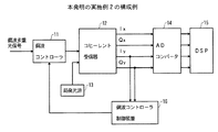
図1〜図3は、本発明の実施例1〜実施例3の構成例を示す。
図1〜図3において、偏波多重光信号を偏波コントローラ11に入力し、その出力と局発光源13から出力されるローカル光をコヒーレント受信器12に入力する。コヒーレント受信器12は、偏波コントローラ11の出力とローカル光をそれぞれ偏波ビームスプリッタ(PBS)でX偏波とY偏波に分離し、各偏波ごとにコヒーレント検波する構成であり、X偏波のIチャネルおよびQチャネルの電気信号出力Ix ,Qxと、Y偏波のIチャネルおよびQチャネルの電気信号出力Iy ,Qy が取り出される。これらの電気信号出力は、ADコンバータ14でデジタル信号に変換した後に、DSP15によるデジタル信号処理により偏波多重信号が復調される。
1 to 3 show configuration examples of Embodiments 1 to 3 of the present invention.
1 to 3, the polarization multiplexed optical signal is input to the polarization controller 11, and the output and local light output from the
実施例1では、コヒーレントレシーバ12から出力されるX偏波のIチャネルおよびQチャネルの電気信号出力Ix ,Qxを分岐し、偏波コントローラ制御装置15へ入力する。偏波コントローラ制御装置15は、X偏波のIチャネルおよびQチャネルの電気信号出力Ix ,QxからX偏波のRFパワーを検出する。
In the first embodiment, the X-polarized I-channel and Q-channel electrical signal outputs Ix and Qx output from the
実施例2では、コヒーレントレシーバ12から出力されるY偏波のIチャネルおよびQチャネルの電気信号出力Iy ,Qy を分岐し、偏波コントローラ制御装置15へ入力する。偏波コントローラ制御装置15は、Y偏波のIチャネルおよびQチャネルの電気信号出力Iy ,Qy からY偏波のRFパワーを検出する。
In the second embodiment, the Y-polarized I-channel and Q-channel electrical signal outputs Iy and Qy output from the
実施例3では、コヒーレントレシーバ12から出力されるX偏波のIチャネルおよびQチャネルの電気信号出力Ix ,QxおよびY偏波のIチャネルおよびQチャネルの電気信号出力Iy ,Qy を分岐し、偏波コントローラ制御装置15へ入力する。偏波コントローラ制御装置15は、X偏波のIチャネルおよびQチャネルの電気信号出力Ix ,QxからX偏波のRFパワーを検出し、Y偏波のIチャネルおよびQチャネルの電気信号出力Iy ,Qy からY偏波のRFパワーを検出する。
In the third embodiment, the X-polarized I-channel and Q-channel electrical signal outputs Ix and Qx output from the
非特許文献5,6によると、偏波多重光信号を偏波ビームスプリッタで分離した後に、フォトダイオードで光電気変換して得られる光電流i1 ,i2 は、
i1 ∝b1cos2ψ/2+b2sin2ψ/2+2b1b2cosφsinψ …(1)
i2 ∝b1sin2ψ/2+b2cos2ψ/2−2b1b2cosφsinψ …(2)
で表される。ここで、φは送信機におけるXY偏波間の位相差、b1 およびb2 はX偏波およびY偏波の情報ビット(b1,b2 ∈{0, 1})、ψは偏波ビームスプリッタの軸に対する入射角度を示している。 (1)式の第2項および第3項は、X偏波に対応する光電流i1 におけるY偏波のクロストーク成分を示す。 (2)式の第1項および第3項は、Y偏波に対応する光電流i2 におけるX偏波のクロストーク成分を示す。
According to Non-Patent Documents 5 and 6, photocurrents i 1 and i 2 obtained by photoelectrically converting a polarization multiplexed optical signal using a photodiode after being separated by a polarization beam splitter are:
i 1 ∝b 1 cos 2 ψ / 2 + b 2 sin 2 ψ / 2 + 2b 1 b 2 cos φsinψ (1)
i 2 ∝b 1 sin 2 ψ / 2 + b 2 cos 2 ψ / 2−2 b 1 b 2 cos φsinψ (2)
It is represented by Where φ is the phase difference between the XY polarizations in the transmitter, b 1 and b 2 are the information bits (b 1 , b 2 ε {0, 1}) of the X and Y polarizations, and ψ is the polarization beam The incident angle with respect to the axis of the splitter is shown. The second term and the third term of the equation (1) indicate the crosstalk component of the Y polarization in the photocurrent i 1 corresponding to the X polarization. The first term and the third term in the equation (2) indicate the crosstalk component of the X polarization in the photocurrent i 2 corresponding to the Y polarization.
したがって、偏波多重光信号の偏波分離におけるXY偏波間のクロストーク成分( (1)式の第2項および第3項、および (2)式の第1項および第3項)を除去するために、ψ=0となるように、すなわち実施例1ではX偏波のRFパワー( (1)式の光電流i 1 に比例)が最小となるように、偏波コントローラ制御装置15が偏波コントローラ11を用いて入力側の偏波状態を最適化すれば、各偏波におけるクロストーク成分が最小化してi1 =b1 、i2 =b2 となる。
Therefore, the crosstalk component between the XY polarizations in the polarization separation of the polarization multiplexed optical signal (the second and third terms in the equation (1) and the first and third terms in the equation (2)) is removed. Therefore, the polarization
これにより、コヒーレント受信器12へ入力される偏波多重光信号の偏波状態を光領域で最適化することができるので、DSP15のデジタル信号処理の負荷の軽減および安定性の向上を図ることができる。また、偏波コントローラ11の自動制御単独では補償することのできないPMDによる波形歪みは、DSP15を用いて補償することにより、簡易で高性能なデジタルコヒーレント受信装置を実現することができる。
As a result, the polarization state of the polarization multiplexed optical signal input to the
11 偏波コントローラ
12 コヒーレント受信器
13 局発光源
14 ADコンバータ
15 DSP
16 偏波コントローラ制御装置
11
16 Polarization controller controller
Claims (1)
前記偏波コントローラから出力される偏波多重光信号とローカル光を入力し、偏波分離してコヒーレント検波を行い、X偏波およびY偏波に対応する電気信号を出力するコヒーレント受信器と、
前記コヒーレント受信器から出力されるX偏波およびY偏波に対応する電気信号をアナログ−デジタル変換して出力するADコンバータと、
前記ADコンバータから出力されるデジタル信号をデジタル信号処理により復調するデジタルシグナルプロセッサと、
前記コヒーレント受信器から出力されるX偏波の電気信号からX偏波のRFパワーを検出し、該X偏波のRFパワーに含まれるY偏波のクロストーク成分を除去するために、該X偏波のRFパワーが最小になるように前記偏波コントローラを制御する偏波コントローラ制御装置と
を備えたことを特徴とするデジタルコヒーレント受信装置。 A polarization controller that changes the polarization state of the polarization multiplexed optical signal;
A coherent receiver that inputs a polarization multiplexed optical signal and local light output from the polarization controller, performs polarization separation to perform coherent detection, and outputs an electrical signal corresponding to X polarization and Y polarization;
An analog-to-digital converter that outputs an electrical signal corresponding to the X polarization and the Y polarization output from the coherent receiver;
A digital signal processor that demodulates a digital signal output from the AD converter by digital signal processing;
Wherein detecting the RF power of the X polarized wave from the electrical signals of X polarization output from the coherent receiver, in order to remove the crosstalk component of the Y polarization contained in the RF power of the X polarization, the X A digital coherent receiver comprising: a polarization controller controller that controls the polarization controller so that the RF power of polarization is minimized.
Priority Applications (1)
| Application Number | Priority Date | Filing Date | Title |
|---|---|---|---|
| JP2011104996A JP5583631B2 (en) | 2011-05-10 | 2011-05-10 | Digital coherent receiver |
Applications Claiming Priority (1)
| Application Number | Priority Date | Filing Date | Title |
|---|---|---|---|
| JP2011104996A JP5583631B2 (en) | 2011-05-10 | 2011-05-10 | Digital coherent receiver |
Publications (2)
| Publication Number | Publication Date |
|---|---|
| JP2012238941A JP2012238941A (en) | 2012-12-06 |
| JP5583631B2 true JP5583631B2 (en) | 2014-09-03 |
Family
ID=47461487
Family Applications (1)
| Application Number | Title | Priority Date | Filing Date |
|---|---|---|---|
| JP2011104996A Active JP5583631B2 (en) | 2011-05-10 | 2011-05-10 | Digital coherent receiver |
Country Status (1)
| Country | Link |
|---|---|
| JP (1) | JP5583631B2 (en) |
Families Citing this family (1)
| Publication number | Priority date | Publication date | Assignee | Title |
|---|---|---|---|---|
| JP5842826B2 (en) * | 2010-12-21 | 2016-01-13 | 日本電気株式会社 | Coherent optical receiver, inter-lane skew detection apparatus and detection method in coherent optical receiver |
Family Cites Families (9)
| Publication number | Priority date | Publication date | Assignee | Title |
|---|---|---|---|---|
| JP5157521B2 (en) * | 2007-03-20 | 2013-03-06 | 富士通株式会社 | Polarization multiplexed optical receiver, polarization multiplexed optical transmission / reception system, and control method for polarization multiplexed optical transmission / reception system |
| JP5034770B2 (en) * | 2007-08-16 | 2012-09-26 | 富士通株式会社 | Coherent optical receiver and optical communication system |
| JP2009198364A (en) * | 2008-02-22 | 2009-09-03 | Fujitsu Ltd | Monitor circuit for monitoring property of optical fiber transmission line and quality of optical signal |
| US8355637B2 (en) * | 2008-02-22 | 2013-01-15 | Nippon Telegraph And Telephone Corporation | Optical OFDM receiver, optical transmission system, subcarrier separation circuit, and subcarrier separation method |
| JP5217792B2 (en) * | 2008-08-29 | 2013-06-19 | 富士通株式会社 | Optical receiver power supply control method, digital signal processing circuit, and optical receiver |
| JP5312190B2 (en) * | 2009-05-14 | 2013-10-09 | 日本電信電話株式会社 | Optical receiving apparatus and optical receiving method |
| JP5437858B2 (en) * | 2010-03-05 | 2014-03-12 | 富士通テレコムネットワークス株式会社 | Optical transmission system |
| JP5683237B2 (en) * | 2010-11-29 | 2015-03-11 | 株式会社日立製作所 | Polarization multiplexed optical transmission system, polarization multiplexed optical transmitter, and polarization multiplexed optical receiver |
| CN103339882B (en) * | 2011-02-01 | 2016-05-11 | 日本电气株式会社 | Coherent optics receiver, for detection of the apparatus and method of the interchannel deflection in coherent optics receiver |
-
2011
- 2011-05-10 JP JP2011104996A patent/JP5583631B2/en active Active
Also Published As
| Publication number | Publication date |
|---|---|
| JP2012238941A (en) | 2012-12-06 |
Similar Documents
| Publication | Publication Date | Title |
|---|---|---|
| JP5141498B2 (en) | Optical transmission / reception system, optical transmitter, optical receiver, and optical transmission / reception method | |
| JP5326584B2 (en) | Delay processing device, signal amplification device, photoelectric conversion device, analog / digital conversion device, reception device, and reception method | |
| JP5700050B2 (en) | Coherent light receiving apparatus and coherent light receiving method | |
| JP4888567B2 (en) | Coherent optical receiver | |
| EP2482486B1 (en) | Sampling clock synchronizing apparatus, digital coherent receiving apparatus, and sampling clock synchronizing method | |
| JP7121887B2 (en) | Digital coherent receiver and its skew adjustment method | |
| US20110058820A1 (en) | Optical transmission system, optical transmission equipment, and chromatic dispersion compensation method | |
| JP5987523B2 (en) | Receiver and failure detection method for receiver | |
| JP5223703B2 (en) | Polarization multiplexed optical receiver, polarization multiplexed optical receiver circuit, and polarization multiplexed optical transmission system | |
| US8958704B2 (en) | Generation of a feedback signal for a polarization mode dispersion compensator in a communication system using alternate-polarization | |
| Poggiolini et al. | Performance dependence on channel baud-rate of PM-QPSK systems over uncompensated links | |
| US8494373B2 (en) | Apparatus and method for compensating polarization mode dispersion | |
| JP2013034065A (en) | Polarization-multiplexing optical receiver, polarization-multiplexing system, and polarization-multiplexing optical receiving method | |
| Xiao et al. | ICI mitigation for dual-carrier superchannel transmission based on m-PSK and m-QAM formats | |
| KR101931957B1 (en) | Optical transmission method and system using polarization-time coding for polarization diversity multiplexed optical transmission | |
| JP6349696B2 (en) | Optical transmitter, optical receiver, and optical communication method | |
| JP5839106B2 (en) | Receiver, transmission system, polarization multiplexed optical signal reception method, receiver control program | |
| CA2730579A1 (en) | Method, device, and system for realizing polarization mode dispersion compensation | |
| JP5583631B2 (en) | Digital coherent receiver | |
| JP2017143485A (en) | Optical receiver and optical receiving method | |
| Sim et al. | Direct-detection receiver for PDM signals | |
| Huang et al. | Filterless reception of 80× 112-Gb/s WDM channels using single-ended photodiodes and digital interference reduction | |
| JP2019208111A (en) | Optical receiver and reception method | |
| Kamran et al. | Signal processing technique for QPSK system with polarization multiplexed carrier | |
| Reza et al. | A simple M-branch diversity receiver model for PMD-induced penalty mitigation in IM-DD optical transmission systems |
Legal Events
| Date | Code | Title | Description |
|---|---|---|---|
| A621 | Written request for application examination |
Free format text: JAPANESE INTERMEDIATE CODE: A621 Effective date: 20130807 |
|
| A977 | Report on retrieval |
Free format text: JAPANESE INTERMEDIATE CODE: A971007 Effective date: 20140417 |
|
| A131 | Notification of reasons for refusal |
Free format text: JAPANESE INTERMEDIATE CODE: A131 Effective date: 20140513 |
|
| A521 | Request for written amendment filed |
Free format text: JAPANESE INTERMEDIATE CODE: A523 Effective date: 20140619 |
|
| TRDD | Decision of grant or rejection written | ||
| A01 | Written decision to grant a patent or to grant a registration (utility model) |
Free format text: JAPANESE INTERMEDIATE CODE: A01 Effective date: 20140715 |
|
| A61 | First payment of annual fees (during grant procedure) |
Free format text: JAPANESE INTERMEDIATE CODE: A61 Effective date: 20140716 |
|
| R150 | Certificate of patent or registration of utility model |
Ref document number: 5583631 Country of ref document: JP Free format text: JAPANESE INTERMEDIATE CODE: R150 |