JP5558005B2 - Interferometer system for monitoring objects - Google Patents
Interferometer system for monitoring objects Download PDFInfo
- Publication number
- JP5558005B2 JP5558005B2 JP2008551478A JP2008551478A JP5558005B2 JP 5558005 B2 JP5558005 B2 JP 5558005B2 JP 2008551478 A JP2008551478 A JP 2008551478A JP 2008551478 A JP2008551478 A JP 2008551478A JP 5558005 B2 JP5558005 B2 JP 5558005B2
- Authority
- JP
- Japan
- Prior art keywords
- interferometer
- optical
- wavefront
- radiation
- light source
- Prior art date
- Legal status (The legal status is an assumption and is not a legal conclusion. Google has not performed a legal analysis and makes no representation as to the accuracy of the status listed.)
- Active
Links
Images


Classifications
-
- G—PHYSICS
- G01—MEASURING; TESTING
- G01B—MEASURING LENGTH, THICKNESS OR SIMILAR LINEAR DIMENSIONS; MEASURING ANGLES; MEASURING AREAS; MEASURING IRREGULARITIES OF SURFACES OR CONTOURS
- G01B9/00—Measuring instruments characterised by the use of optical techniques
- G01B9/02—Interferometers
- G01B9/02001—Interferometers characterised by controlling or generating intrinsic radiation properties
- G01B9/02002—Interferometers characterised by controlling or generating intrinsic radiation properties using two or more frequencies
- G01B9/02004—Interferometers characterised by controlling or generating intrinsic radiation properties using two or more frequencies using frequency scans
-
- G—PHYSICS
- G01—MEASURING; TESTING
- G01B—MEASURING LENGTH, THICKNESS OR SIMILAR LINEAR DIMENSIONS; MEASURING ANGLES; MEASURING AREAS; MEASURING IRREGULARITIES OF SURFACES OR CONTOURS
- G01B9/00—Measuring instruments characterised by the use of optical techniques
- G01B9/02—Interferometers
- G01B9/02001—Interferometers characterised by controlling or generating intrinsic radiation properties
- G01B9/02002—Interferometers characterised by controlling or generating intrinsic radiation properties using two or more frequencies
-
- G—PHYSICS
- G01—MEASURING; TESTING
- G01B—MEASURING LENGTH, THICKNESS OR SIMILAR LINEAR DIMENSIONS; MEASURING ANGLES; MEASURING AREAS; MEASURING IRREGULARITIES OF SURFACES OR CONTOURS
- G01B9/00—Measuring instruments characterised by the use of optical techniques
- G01B9/02—Interferometers
- G01B9/02001—Interferometers characterised by controlling or generating intrinsic radiation properties
- G01B9/02007—Two or more frequencies or sources used for interferometric measurement
-
- G—PHYSICS
- G01—MEASURING; TESTING
- G01B—MEASURING LENGTH, THICKNESS OR SIMILAR LINEAR DIMENSIONS; MEASURING ANGLES; MEASURING AREAS; MEASURING IRREGULARITIES OF SURFACES OR CONTOURS
- G01B9/00—Measuring instruments characterised by the use of optical techniques
- G01B9/02—Interferometers
- G01B9/02015—Interferometers characterised by the beam path configuration
- G01B9/02027—Two or more interferometric channels or interferometers
-
- G—PHYSICS
- G01—MEASURING; TESTING
- G01B—MEASURING LENGTH, THICKNESS OR SIMILAR LINEAR DIMENSIONS; MEASURING ANGLES; MEASURING AREAS; MEASURING IRREGULARITIES OF SURFACES OR CONTOURS
- G01B9/00—Measuring instruments characterised by the use of optical techniques
- G01B9/02—Interferometers
- G01B9/0209—Low-coherence interferometers
-
- G—PHYSICS
- G03—PHOTOGRAPHY; CINEMATOGRAPHY; ANALOGOUS TECHNIQUES USING WAVES OTHER THAN OPTICAL WAVES; ELECTROGRAPHY; HOLOGRAPHY
- G03F—PHOTOMECHANICAL PRODUCTION OF TEXTURED OR PATTERNED SURFACES, e.g. FOR PRINTING, FOR PROCESSING OF SEMICONDUCTOR DEVICES; MATERIALS THEREFOR; ORIGINALS THEREFOR; APPARATUS SPECIALLY ADAPTED THEREFOR
- G03F7/00—Photomechanical, e.g. photolithographic, production of textured or patterned surfaces, e.g. printing surfaces; Materials therefor, e.g. comprising photoresists; Apparatus specially adapted therefor
- G03F7/70—Microphotolithographic exposure; Apparatus therefor
- G03F7/70691—Handling of masks or workpieces
- G03F7/70775—Position control, e.g. interferometers or encoders for determining the stage position
-
- G—PHYSICS
- G01—MEASURING; TESTING
- G01B—MEASURING LENGTH, THICKNESS OR SIMILAR LINEAR DIMENSIONS; MEASURING ANGLES; MEASURING AREAS; MEASURING IRREGULARITIES OF SURFACES OR CONTOURS
- G01B2210/00—Aspects not specifically covered by any group under G01B, e.g. of wheel alignment, caliper-like sensors
- G01B2210/60—Unique sensor identification
-
- G—PHYSICS
- G01—MEASURING; TESTING
- G01B—MEASURING LENGTH, THICKNESS OR SIMILAR LINEAR DIMENSIONS; MEASURING ANGLES; MEASURING AREAS; MEASURING IRREGULARITIES OF SURFACES OR CONTOURS
- G01B2290/00—Aspects of interferometers not specifically covered by any group under G01B9/02
- G01B2290/15—Cat eye, i.e. reflection always parallel to incoming beam
-
- G—PHYSICS
- G01—MEASURING; TESTING
- G01B—MEASURING LENGTH, THICKNESS OR SIMILAR LINEAR DIMENSIONS; MEASURING ANGLES; MEASURING AREAS; MEASURING IRREGULARITIES OF SURFACES OR CONTOURS
- G01B2290/00—Aspects of interferometers not specifically covered by any group under G01B9/02
- G01B2290/45—Multiple detectors for detecting interferometer signals
Landscapes
- Physics & Mathematics (AREA)
- General Physics & Mathematics (AREA)
- Length Measuring Devices By Optical Means (AREA)
- Instruments For Measurement Of Length By Optical Means (AREA)
Description
本出願は、2006年1月23日出願の、「物体の位置及び方位をモニタするファイバセンサシステム」という名称の米国特許仮出願第60/761,314号と、2006年3月15日出願の、「物体の位置及び方位をモニタするファイバセンサシステム」という名称の米国特許仮出願第60/782,722号と、2006年8月31日出願の、「物体の位置及び方位をモニタするファイバセンサシステム」という名称の米国特許仮出願第60/841,442号の優先権を主張するものである。これら各出願の内容全体は、参照により本明細書に組み込まれる。 This application is filed on Jan. 23, 2006, US Provisional Application No. 60 / 761,314 entitled “Fiber Sensor System for Monitoring Object Position and Orientation” and filing on Mar. 15, 2006. US Provisional Application No. 60 / 782,722 entitled "Fiber Sensor System for Monitoring Object Position and Orientation" and "Fiber Sensor for Monitoring Object Position and Orientation" filed Aug. 31, 2006 The priority of US Provisional Patent Application No. 60 / 841,442 entitled "System" is claimed. The entire contents of each of these applications are incorporated herein by reference.
多くの精密エンジニアリングシステムについては、長い期間、例えば、日単位、月単位、又は、年単位さえにわたってnmレベルの公差まで物体の位置を測定することが必要とされている。物体の動きの範囲は、小さい、例えば、任意の方向においてmm未満である場合があるが、安定性が得られるように能動サーボループで、かつ、制御された微調整に備えるように制御するべきである。 For many precision engineering systems, it is necessary to measure the position of an object to a tolerance of the nm level over a long period of time, for example daily, monthly or even yearly. The range of motion of the object may be small, eg, less than mm in any direction, but should be controlled with an active servo loop to provide stability and for controlled fine tuning It is.
このような精密エンジニアリングシステムの一例は、最新のフォトリソグラフィツールの投影レンズ(PO)部品である。PO部品の各種の例は、J.R.Sheats、B.W.Smith共編「マイクロリソグラフィ:科学技術」、Marcel Decker社(ニューヨーク州ニューヨーク、1998年)で説明されている。PO部品としては、光屈折PO部品、反射屈折PO部品、反射PO部品がある。 An example of such a precision engineering system is the projection lens (PO) component of a modern photolithography tool. Various examples of PO parts are described in J.P. R. Sheets, B.I. W. Co-edited by Smith, "Microlithography: Science and Technology", described by Marcel Decker (New York, NY, 1998). As the PO parts, there are a photorefractive PO part, a catadioptric PO part, and a reflective PO part.
このようなPO部品においては、相対位置を測定する各種レンズ素子及びセルで構成されるPO部品を通して設置された各種センサと関連して動作する各種小型アクチュエータにより、互いとの関係及び/又はPO部品レンズセルとの関係で、各種レンズで構成された様々な副部品が保持される。これらのセンサは、例えば、「精密機械設計」、ニュージャージ州エングルウッドクリフ、Prentice Hall、162ページから173ページ(1992年)において、A.H.Slocumにより説明されているような符号器デバイスとすることができ、かつ、位置フィードバック制御に使用されている。 In such PO parts, the relationship with each other and / or the PO parts by various small actuators that operate in association with various sensors installed through the PO parts composed of various lens elements and cells that measure relative positions. Various sub-parts composed of various lenses are held in relation to the lens cell. These sensors are described, for example, in “Precision Mechanical Design”, Englewood Cliff, NJ, Prentice Hall, pages 162 to 173 (1992). H. It can be an encoder device as described by Slocum and is used for position feedback control.
本開示は、取付けフレーム又は別の光学部品に関する光学部品の位置など、別の構成部品に対する1つの構成部品の位置をモニタするセンサ及びセンサシステムを特徴とする。本センサシステムは、複数の受動干渉計光センサにより、1つ又はそれ以上の構成部品の少なくとも1つの自由度を測定する。一般に、各センサは、1つの自由度に感応し、他の自由度には実質的に感応しない。各光センサは、光ファイバなど、少なくとも1つのファイバ導波路からの光により照射され、センサからの光信号は、少なくとも1つのファイバ導波路により遠隔共通光源/検出器サブシステムに伝達される。光源/検出器サブシステムは、全ての光センサにとって単一の光源となることができる。光は、波長同調可能な離散的波長又は多重化された一連の離散的波長又はその両方とすることができる。 The present disclosure features sensors and sensor systems that monitor the position of one component relative to another component, such as the position of the optical component relative to a mounting frame or another optical component. The sensor system measures at least one degree of freedom of one or more components by a plurality of passive interferometer optical sensors. In general, each sensor is sensitive to one degree of freedom and substantially insensitive to the other degrees of freedom. Each optical sensor is illuminated by light from at least one fiber waveguide, such as an optical fiber, and the optical signal from the sensor is transmitted to the remote common light source / detector subsystem by at least one fiber waveguide. The light source / detector subsystem can be a single light source for all light sensors. The light can be a wavelength tunable discrete wavelength or a multiplexed series of discrete wavelengths or both.
特定の実施形態においては、光源/検出器ユニットは、2つの動作モードを有することができる。1つのモードにおいては、光源/検出器ユニットは、随時必要とされると考えられる絶対位置を判断するためにセンサについて絶対原位置を確立する。もう1つのモードにおいては、光源/検出器ユニットは、位置制御サーボシステムに連続的なデータを供給するために、高速、例えば、1kHzにて、物体自由度の任意の変化を測定する。センサ断熱化手段も設置される。 In certain embodiments, the light source / detector unit can have two modes of operation. In one mode, the light source / detector unit establishes an absolute home position for the sensor to determine the absolute position that may be needed from time to time. In another mode, the light source / detector unit measures any change in object freedom at high speed, eg, 1 kHz, to provide continuous data to the position control servo system. Sensor insulation means are also installed.
一部の実施形態においては、センサは、動作モードを切り替える必要がなく、連続的な、高速絶対距離測定結果を供給する。
幾つかのタイプのセンサ、光センサ/検出器ユニット、及び光ファイバアーキテクチャを使用することができる。
In some embodiments, the sensor does not need to switch operating modes and provides continuous, high speed absolute distance measurement results.
Several types of sensors, optical sensor / detector units, and fiber optic architectures can be used.
一般に、第1の態様においては、本発明は、第2の物体に相対的に移動可能に取り付けられた第1の物体を含むシステムを特徴とする。本システムは、各々が、入力放射から第1の波面及び第2の波面を導出し、かつ、第1及び第2の波面を合成して第1及び第2の波面の経路間の光路長の差に関する情報を含む出力放射を供給するように構成された複数の干渉計を含み、各々の干渉計は、第1の波面の経路内に位置決めされた反射素子を含み、干渉計の少なくとも1つの反射素子は、第1の物体上に取り付けられる。本システムは、複数のファイバ導波路及び電子制御装置も含む。各ファイバ導波路は、入力放射を対応する干渉計に送出するか、又は、出力放射を対応する干渉計から対応する検出器に送出するように構成される。電子制御装置は、干渉計の少なくとも1つからの情報に基づいて、第2の物体に関する第1の物体の自由度をモニタするように構成され、自由度は、第1及び第2の物体間の絶対変位である。 In general, in a first aspect, the invention features a system that includes a first object that is movably attached to a second object. Each of the systems derives a first wavefront and a second wavefront from the input radiation and combines the first and second wavefronts to determine the optical path length between the first and second wavefront paths. A plurality of interferometers configured to provide output radiation including information about the difference, each interferometer including a reflective element positioned in a path of the first wavefront, wherein at least one of the interferometers The reflective element is mounted on the first object. The system also includes a plurality of fiber waveguides and an electronic controller. Each fiber waveguide is configured to deliver input radiation to a corresponding interferometer or output radiation from a corresponding interferometer to a corresponding detector. The electronic control unit is configured to monitor the degree of freedom of the first object with respect to the second object based on information from at least one of the interferometers, the degree of freedom between the first and second objects. Is the absolute displacement.
本システムの種々の実施形態は、以下の特徴及び/又は他の態様の特徴の1つ又はそれ以上を含むことができる。例えば、一部の実施形態においては、各ファイバ導波路は、入力放射を対応する干渉計に送出して、出力放射を対応する干渉計から対応する検出器に送出するように構成される。各干渉計用入力放射は、約900nmから約1,600nm(例えば、約1,500nmから約1,600nm)の範囲の波長を有することができる。各干渉計用入力放射は、他の干渉計と異なる波長を有することができる。 Various embodiments of the present system can include one or more of the following features and / or features of other aspects. For example, in some embodiments, each fiber waveguide is configured to deliver input radiation to a corresponding interferometer and to deliver output radiation from the corresponding interferometer to a corresponding detector. Each interferometer input radiation may have a wavelength in the range of about 900 nm to about 1,600 nm (eg, about 1,500 nm to about 1,600 nm). Each interferometer input radiation may have a different wavelength than the other interferometers.
各干渉計は、入力放射の経路内に位置決めされた光インタフェースを含むことができ、光インタフェースは、入力放射の第1の部分を反射して第1又は第2の波面を形成するように構成される。光インタフェースは、ファイバ導波路の表面とすることができる。光インタフェースは、平面光インタフェースとすることができる。光インタフェースは、透明素子の表面とすることができる。表面は、入力放射の第2の部分を伝達して第2又は第1の波面を形成するように構成することができる。一部の実施形態においては、各干渉計は、入力放射を測定波面及び基準波面に分割するように構成されたビーム分割器を含む。各ビーム分割器は、偏光ビーム分割器又は非偏光ビーム分割器とすることができる。 Each interferometer can include an optical interface positioned in the path of the input radiation, the optical interface configured to reflect a first portion of the input radiation to form a first or second wavefront. Is done. The optical interface can be the surface of a fiber waveguide. The optical interface can be a planar optical interface. The optical interface can be the surface of a transparent element. The surface can be configured to transmit a second portion of input radiation to form a second or first wavefront. In some embodiments, each interferometer includes a beam splitter configured to split the input radiation into a measurement wavefront and a reference wavefront. Each beam splitter may be a polarized beam splitter or a non-polarized beam splitter.
各干渉計は、第1の波面が物体から1回又は2回以上反射するように構成することができる。
各反射素子は、逆反射体又は鏡とすることができる。
Each interferometer can be configured such that the first wavefront reflects from the object one or more times.
Each reflective element can be a retroreflector or a mirror.
干渉計の少なくとも1つについては、第1の波面は、反射素子から反射することができ、反射素子は、第1の波面を受け取るように構成された表面を含むことができ、この表面は、反射素子から反射する前に第1の波面の横断面寸法より小さい寸法を有する。あるいは、または、更に、干渉計の少なくとも1つについては、第1の波面は、反射素子から反射することができ、反射素子は、第1の波面を受け取るように構成された表面を含むことができ、この表面は、反射素子から反射する前に第1の波面の横断面寸法より大きい寸法を有する。 For at least one of the interferometers, the first wavefront can be reflected from the reflective element, and the reflective element can include a surface configured to receive the first wavefront, the surface comprising: Before reflecting from the reflecting element, the first wavefront has a smaller cross-sectional dimension. Alternatively or additionally, for at least one of the interferometers, the first wavefront can be reflected from the reflective element, and the reflective element can include a surface configured to receive the first wavefront. The surface can have a dimension that is greater than the cross-sectional dimension of the first wavefront before reflecting from the reflective element.
一部の実施形態においては、干渉計の少なくとも1つは、それぞれのファイバ導波路から出現する入力放射を成形するように構成された光学素子を更に含む。光学素子は、レンズとすることができる。レンズは、それぞれの光ファイバから出現する入力放射を視準するように構成することができる。レンズは、第1又は第2の波面を反射する表面を含むことができる。 In some embodiments, at least one of the interferometers further includes an optical element configured to shape the input radiation emerging from the respective fiber waveguide. The optical element can be a lens. The lens can be configured to collimate input radiation emerging from each optical fiber. The lens can include a surface that reflects the first or second wavefront.
干渉計の少なくとも1つは、第1又は第2の波面は、第1の物体にて約0.2mm以下の直径を有することができる。レンズは、光ファイバから出現する光を集束するように構成することができる。反射素子は、集束光の腰部に又は集束光の腰部の近くに位置決めすることができる。 In at least one of the interferometers, the first or second wavefront may have a diameter of about 0.2 mm or less at the first object. The lens can be configured to focus light emerging from the optical fiber. The reflective element can be positioned at or near the waist of the focused light.
本システムは、入力放射を生成するように構成された光源を含むことができ、本システムは、複数のファイバ導波路を介して干渉計に入力放射を送出するように構成される。光源は、広帯域光源を備えることができる。一部の実施形態においては、本システムは、異なる波長の入力放射を広帯域光源から干渉計に伝達するように構成された複数の光フィルタを含む。各光フィルタは、複数の干渉計の1つに対応することができる。広帯域光源は、発光ダイオード又は増幅自然発光源とすることができる。光源は、分散フィードバックレーザなど、レーザを含むことができる。本システムは、光源からの放射を増幅して増幅放射を干渉計に方向づけるように構成された増幅器を含むことができる。光源は、各々が異なる波長にて放射を生成するように構成される複数の光源素子を含むことができる。 The system can include a light source configured to generate input radiation, and the system is configured to deliver the input radiation to the interferometer via a plurality of fiber waveguides. The light source can comprise a broadband light source. In some embodiments, the system includes a plurality of optical filters configured to transmit different wavelengths of input radiation from the broadband light source to the interferometer. Each optical filter can correspond to one of a plurality of interferometers. The broadband light source can be a light emitting diode or an amplified spontaneous light source. The light source can include a laser, such as a distributed feedback laser. The system can include an amplifier configured to amplify the radiation from the light source and direct the amplified radiation to the interferometer. The light source can include a plurality of light source elements each configured to generate radiation at a different wavelength.
本システムは、更なるファイバ導波路を含むことができる。複数のファイバ導波路及び更なるファイバ導波路は、入力放射を干渉計に送出し、かつ、出力放射を干渉計から検出器に送出するように構成されたファイバネットワークを形成する。 The system can include additional fiber waveguides. The plurality of fiber waveguides and the further fiber waveguide form a fiber network that is configured to deliver input radiation to the interferometer and to deliver output radiation from the interferometer to the detector.
一部の実施形態においては、本システムは、干渉計に光学的に結合された遠隔光空洞共振器を含む。遠隔光空洞共振器は、第1の光路及び第2の光路を含むことができ、かつ、第1及び第2の光路の間で異なる光路を変えるように構成された素子を更に備える。 In some embodiments, the system includes a remote optical cavity resonator optically coupled to the interferometer. The remote optical cavity may further include an element that may include a first optical path and a second optical path, and that is configured to change a different optical path between the first and second optical paths.
第1の物体は、光学部品とすることができ、第2の物体は、光学部品が取り付けられるフレームである。第1の物体は、光学撮像システム内の光学部品とすることができる。光学撮像システムは、マイクロリソグラフィツールの投影レンズ部品又は望遠鏡とすることができる。 The first object can be an optical component and the second object is a frame to which the optical component is attached. The first object can be an optical component in the optical imaging system. The optical imaging system can be a projection lens component or a telescope of a microlithography tool.
本システムは、第1の物体に結合されたアクチュエータを含むことができ、アクチュエータは、電子制御装置と通信しており、かつ、電子制御装置により判断された情報に基づいて第1の物体の位置を調整するように構成される。 The system can include an actuator coupled to the first object, the actuator being in communication with the electronic controller and the position of the first object based on information determined by the electronic controller. Configured to adjust.
一般に、別の態様においては、本発明は、第2の物体に関する第1の物体の自由度をモニタする方法を特徴とする。本方法は、光源からの放射を複数の干渉計に方向づけるステップであって、各干渉計が、ファイバ導波路から放射を受光し、放射から第1の波面及び第2の波面を導出し、かつ、第1及び第2の波面を合成して第1及び第2の波面の経路間の光路長の差に関する情報を備える出力放射を供給するように構成され、干渉計の少なくとも1つが、第1の物体上に位置決めされた素子から反射するように第1の波面を方向づけるように構成されるステップを含む。本方法は、出力放射を各干渉計からそれぞれの検出器に方向づけるステップと、干渉計の少なくとも1つからの出力放射からの情報に基づいて、第2の物体に関する第1の物体の自由度に関する情報を判断するステップとを含み、情報は、第1及び第2の物体間の絶対変位を含む。 In general, in another aspect, the invention features a method of monitoring a degree of freedom of a first object with respect to a second object. The method directs radiation from a light source to a plurality of interferometers, each interferometer receiving radiation from a fiber waveguide, deriving a first wavefront and a second wavefront from the radiation, and The first and second wavefronts are combined to provide output radiation comprising information regarding the optical path length difference between the first and second wavefront paths, wherein at least one of the interferometers is Configured to direct the first wavefront to reflect from elements positioned on the object. The method relates to directing output radiation from each interferometer to a respective detector and based on information from the output radiation from at least one of the interferometers, the degree of freedom of the first object with respect to the second object. Determining information, the information including an absolute displacement between the first and second objects.
本方法の種々の実施形態は、以下の特徴及び/又は他の態様の特徴の1つ又はそれ以上を含むことができる。例えば、本方法は、2つ又はそれ以上の干渉計からの出力放射からの情報に基づいて、第1の物体の2つまたはそれ以上の自由度に関する情報を判断するステップを含むことができる。本方法は、干渉計の少なくとも1つからの出力放射からの情報に基づいて、第1又は第2の物体に対する第3の物体の自由度に関する情報を判断するステップを含むことができる。各干渉計に方向づけられた放射は、共通のファイバ導波路を介して方向づけることができる。情報は、第1の物体と第2の物体との間の変位の変動を含むことができる。 Various embodiments of the method can include one or more of the following features and / or features of other aspects. For example, the method can include determining information regarding two or more degrees of freedom of the first object based on information from output radiation from the two or more interferometers. The method can include determining information regarding the degree of freedom of the third object relative to the first or second object based on information from the output radiation from at least one of the interferometers. Radiation directed to each interferometer can be directed through a common fiber waveguide. The information can include variation in displacement between the first object and the second object.
本方法は、モニタされた自由度に基づいて、第1の物体の位置を調整するステップを含むことができる。本方法は、モニタされた自由度に基づいて、第1の物体の位置に関する情報を出力するステップを含むことができる。本方法は、約5kHz以上(例えば、約10kHz以上、約100kHz以上、約500kHz以上、約1MHz以上)の速度にて自由度に関する情報を更新するステップを含むことができる。出力放射は、対応するファイバ導波路を介してそれぞれの検出器に方向づけることができる。絶対変位に関する前記情報が、1nm以上(例えば、0.5nm以上、0.1nm以上)の精度まで判断することができる。 The method can include adjusting the position of the first object based on the monitored degrees of freedom. The method can include outputting information regarding the position of the first object based on the monitored degrees of freedom. The method can include updating the information about the degree of freedom at a rate of about 5 kHz or more (eg, about 10 kHz or more, about 100 kHz or more, about 500 kHz or more, about 1 MHz or more). The output radiation can be directed to the respective detectors via corresponding fiber waveguides. The information regarding the absolute displacement can be determined to an accuracy of 1 nm or more (for example, 0.5 nm or more, 0.1 nm or more).
一般に、更なる態様においては、本発明は、第2の物体に相対的に移動可能に取り付けられた第1の物体を含むシステムを特徴とする。本システムは、各々が、入力放射から第1の波面及び第2の波面を導出し、かつ、第1及び第2の波面を合成して第1及び第2の波面の経路間の光路長の差に関する情報を含む出力放射を供給するように構成された複数の干渉計を含み、各干渉計は、第1の波面の経路内に位置決めされた反射素子を含み、干渉計の少なくとも1つの反射素子は、第1の物体上に取り付けられる。本システムは、各々が、入力放射を対応する干渉計に送出するか、及び/又は、出力放射を対応する干渉計から対応する検出器に送出するように構成される複数のファイバ導波路を含む。本システムは、干渉計の少なくとも1つからの情報に基づいて、第2の物体に関する第1の物体の自由度をモニタするように構成された電子制御装置を含み、第1の物体は、光学撮像システムの屈折素子又は反射素子である。光学撮像システムは、望遠鏡、又は、マイクロリソグラフィツールの投影レンズとすることができる。種々の実施形態は、他の態様の特徴の1つ又はそれ以上を含むことができる。 In general, in a further aspect, the invention features a system that includes a first object that is movably attached to a second object. Each of the systems derives a first wavefront and a second wavefront from the input radiation and combines the first and second wavefronts to determine the optical path length between the first and second wavefront paths. A plurality of interferometers configured to provide output radiation including information regarding the difference, each interferometer including a reflective element positioned in the path of the first wavefront, and at least one reflection of the interferometer; The element is mounted on the first object. The system includes a plurality of fiber waveguides each configured to deliver input radiation to a corresponding interferometer and / or output radiation from a corresponding interferometer to a corresponding detector. . The system includes an electronic controller configured to monitor the degree of freedom of the first object with respect to the second object based on information from at least one of the interferometers, the first object comprising an optical It is a refractive element or a reflective element of an imaging system. The optical imaging system can be a telescope or a projection lens of a microlithography tool. Various embodiments can include one or more of the features of other aspects.
一般に、別の態様においては、本発明は、第2の物体に相対的に移動可能に取り付けられた第1の物体を含むシステムを特徴とする。本システムは、入力放射を供給するように構成された低コヒーレンス光源、及び、各々が入力放射から第1の波面及び第2の波面を導出し、かつ、第1及び第2の波面を合成して第1及び第2の波面の経路間の光路長の差に関する情報を含む出力放射を供給するように構成された複数の干渉計を含み、各干渉計は、第1の波面の経路内に位置決めされた反射素子を含み、干渉計の少なくとも1つの反射素子は、第1の物体上に取り付けられる。本システムは、また、各々が入力放射を対応する干渉計に送出するか、及び/又は、出力放射を対応する干渉計から対応する検出器に送出するように構成される複数のファイバ導波路を含む。本システムは、干渉計の少なくとも1つからの情報に基づいて、第2の物体に関する第1の物体の自由度をモニタするように構成された電子制御装置を含む。光源は、約1メートル以下(例えば、約1cm以下、1mm以下、0.5mm以下)のコヒーレンス長を有することができる。光源は、広帯域光源とすることができる。本システムの種々の実施形態は、他の態様の特徴を含むことができる。 In general, in another aspect, the invention features a system that includes a first object that is movably attached to a second object. The system includes a low coherence light source configured to provide input radiation, each deriving a first wavefront and a second wavefront from the input radiation, and combining the first and second wavefronts. A plurality of interferometers configured to provide output radiation including information regarding a difference in optical path length between the first and second wavefront paths, each interferometer being within the path of the first wavefront At least one reflective element of the interferometer is mounted on the first object, including a positioned reflective element. The system also includes a plurality of fiber waveguides each configured to deliver input radiation to a corresponding interferometer and / or output radiation from a corresponding interferometer to a corresponding detector. Including. The system includes an electronic controller configured to monitor the degree of freedom of the first object with respect to the second object based on information from at least one of the interferometers. The light source can have a coherence length of about 1 meter or less (eg, about 1 cm or less, 1 mm or less, 0.5 mm or less). The light source can be a broadband light source. Various embodiments of the system can include features of other aspects.
一般に、別の態様においては、本発明は、構成部品フレームを介して部品内に取り付けられた1つ又はそれ以上の構成部品の位置をモニタするシステムを特徴とする。本システムは、各々が構成部品の1つの自由度のみに感応する1つ又はそれ以上の受動干渉計センサを含み、各受動干渉計センサは、入力ビームから第1のビーム及び第2のビームを導出し、第1の物体から反射するように第1又は第2ビームを方向づけ、かつ、第1及び第2のビームを再合成して第1及び第2のビームの経路間の光路差に関する情報を備える出力ビームを形成するように構成され、入力ビームは、光ファイバケーブルを介して照射部品からセンサに送出され、出力ビームは、同じ又は異なる光ファイバケーブルを介して検出部品に送出され、各センサについては、第1の物体又は受動干渉計センサは、構成部品フレームに装着される。 In general, in another aspect, the invention features a system for monitoring the position of one or more components mounted within a component via a component frame. The system includes one or more passive interferometer sensors, each sensitive to only one degree of freedom of the component, each passive interferometer sensor deriving a first beam and a second beam from an input beam. Information about the optical path difference between the paths of the first and second beams by deriving, directing the first or second beam to reflect from the first object, and recombining the first and second beams The input beam is delivered from the illumination component to the sensor via a fiber optic cable, and the output beam is delivered to the detection component via the same or different fiber optic cable, each For sensors, the first object or passive interferometer sensor is mounted on the component frame.
本システムの種々の実施形態は、以下の特徴及び/又は他の態様の特徴の1つ又はそれ以上を含むことができる。例えば、一部の実施形態においては、部品は、投影レンズ部品である。 Various embodiments of the present system can include one or more of the following features and / or features of other aspects. For example, in some embodiments, the part is a projection lens part.
照射部品は、入力ビームを受動干渉計センサに送出するように構成された光源を含むことができる。光源は、レーザ(例えば、分散フィードバックレーザ)を含むことができる。光源は、広帯域光源とすることができる。光源は、各々が異なる波長の光を生成するように構成された複数の光源素子を含むことができる。各光源素子は、レーザを含むことができる。一部の実施形態においては、本システムは、光源素子から光を受光し、かつ、光を受動干渉計センサに送出するように配設された導波路に光を結合するように構成された分波合波器を含む。 The illumination component can include a light source configured to deliver an input beam to the passive interferometer sensor. The light source can include a laser (eg, a distributed feedback laser). The light source can be a broadband light source. The light source can include a plurality of light source elements each configured to generate light of a different wavelength. Each light source element can include a laser. In some embodiments, the system is configured to couple light into a waveguide arranged to receive light from the light source element and to deliver light to the passive interferometer sensor. Includes a wave multiplexer.
この構成部品は、それぞれの受動干渉計センサから約10cm以下(例えば、約1cm以下)のところに位置することができる。
各受動干渉計センサは、入力ビームの経路内に位置決めされた光インタフェースを含むことができ、光インタフェースは、入力ビームの第1の部分を反射して第1又は第2のビームを形成するように構成される。光インタフェースは、光ファイバの表面とすることができる。光インタフェースは、平面光インタフェースとすることができる。光インタフェースは、透明素子の表面とすることができる。表面は、入力ビームの第2の部分を透過して第2又は第1のビームを形成するように構成することができる。
The component can be located about 10 cm or less (eg, about 1 cm or less) from each passive interferometer sensor.
Each passive interferometer sensor can include an optical interface positioned in the path of the input beam such that the optical interface reflects a first portion of the input beam to form a first or second beam. Configured. The optical interface can be the surface of an optical fiber. The optical interface can be a planar optical interface. The optical interface can be the surface of a transparent element. The surface can be configured to transmit a second portion of the input beam to form a second or first beam.
各受動干渉計センサは、入力ビームを測定ビーム及び基準ビームに分割するように構成されたビーム分割器を含むことができる。各ビーム分割器は、偏光ビーム分割器とすることができる。 Each passive interferometer sensor can include a beam splitter configured to split the input beam into a measurement beam and a reference beam. Each beam splitter may be a polarization beam splitter.
各受動干渉計センサは、第1のビームが物体から1回反射するように構成することができる。あるいは、一部の実施形態においては、各受動干渉計センサは、第1のビームが物体から2回以上反射するように構成することができる。 Each passive interferometer sensor can be configured such that the first beam reflects once from the object. Alternatively, in some embodiments, each passive interferometer sensor can be configured such that the first beam reflects from the object more than once.
各第1の物体は、それぞれの逆反射体及び/又は鏡(例えば、平面鏡又は曲面鏡)を含むことができる。
本システムは、光ファイバから出現する光を成形するように構成された光学素子(例えば、1つ又は複数のレンズ)を含むことができる。光学素子は、光ファイバから出現する光を視準するように構成することができる。一部の実施形態においては、光学素子は、光ファイバから出現する光を集光するように構成される。
Each first object can include a respective retroreflector and / or mirror (eg, a plane mirror or a curved mirror).
The system can include an optical element (eg, one or more lenses) configured to shape light emerging from the optical fiber. The optical element can be configured to collimate light emerging from the optical fiber. In some embodiments, the optical element is configured to collect light emerging from the optical fiber.
検出部品は、1つ又はそれ以上の受動干渉計センサからの出力ビームを受光するように構成された検出器を含むことができる。検出器は、単一素子検出器とすることができる。検出器は、対応する第1の物体から約20cm以上離れたところに位置することができる。検出器は、対応する第1の物体から約100cm以上離れたところに位置することができる。検出器は、構成部品から遠いところに位置決めすることができる。本システムは、検出器に結合された電子プロセッサを含むこともでき、電子プロセッサは、受動干渉計センサの1つからの出力ビームに応答して検出器からの信号に基づいて、物体の位置に関する情報を判断するように構成される。本システムは、構成部品に結合されたアクチュエータを含むことができ、アクチュエータは、電子プロセッサを通信しており、かつ、電子プロセッサにより判断された情報に基づいて構成部品の位置を調整するように構成される。 The detection component can include a detector configured to receive an output beam from one or more passive interferometer sensors. The detector can be a single element detector. The detector can be located about 20 cm or more away from the corresponding first object. The detector can be located about 100 cm or more away from the corresponding first object. The detector can be positioned remotely from the component. The system may also include an electronic processor coupled to the detector, the electronic processor relating to the position of the object based on the signal from the detector in response to the output beam from one of the passive interferometer sensors. It is configured to determine information. The system can include an actuator coupled to the component, the actuator being in communication with the electronic processor and configured to adjust the position of the component based on information determined by the electronic processor. Is done.
各受動干渉計センサについては、第1のビームは、偏光するか、又は、非偏光とすることができる。
構成部品は、屈折構成部品(例えば、レンズ)、反射構成部品(例えば、鏡)、又は、回折構成部品(例えば、回折格子)とすることができる。部品は、更なる構成部品を含むことができ、本システムは、他の構成部品の位置をモニタするように構成される。
For each passive interferometer sensor, the first beam can be polarized or unpolarized.
The component can be a refractive component (eg, a lens), a reflective component (eg, a mirror), or a diffractive component (eg, a diffraction grating). The part can include additional components, and the system is configured to monitor the position of other components.
別の態様においては、本発明は、先のシステムを含むフォトリソグラフィツールを特徴とする。
一般に、別の態様においては、本発明は、フレーム内に取り付けられた複数の光学素子と、各々が光学素子の1つとフレームとの間で光を方向づけるように配設された複数のセンサと、光学素子とフレームとの間でセンサにより方向づけられた後に光を検出するように構成される、投影レンズ部品から遠い場所にて位置決めされた複数の検出器を含む投影レンズ部品を含むシステムを特徴とする。
In another aspect, the invention features a photolithography tool that includes the previous system.
In general, in another aspect, the invention comprises a plurality of optical elements mounted in a frame, and a plurality of sensors each disposed to direct light between one of the optical elements and the frame; A system comprising a projection lens component including a plurality of detectors positioned at locations remote from the projection lens component configured to detect light after being directed by a sensor between an optical element and a frame To do.
本システムの種々の実施形態は、以下の特徴及び/又は他の態様の特徴の1つ又はそれ以上を含むことができる。例えば、本システムは、センサの少なくとも1つからの光を検出器の少なくとも1つに方向づけるように構成された光ファイバを含むことができる。 Various embodiments of the present system can include one or more of the following features and / or features of other aspects. For example, the system can include an optical fiber configured to direct light from at least one of the sensors to at least one of the detectors.
一般に、別の態様においては、本発明は、光学部品を備える投影レンズ部品に装着された干渉計と、干渉計に光を方向づけるように構成された光源と、干渉計から光を受光するように構成された検出器とを含むシステムを特徴とする。動作中、干渉計は、光源からの入力光を受光して、出力光を検出器に方向づけ、出力光は、投影レンズ部品内の光学部品の位置に関する情報を備える。本システムの種々の実施形態は、他の態様の特徴の1つ又はそれ以上を含むことができる。 In general, in another aspect, the invention provides an interferometer mounted on a projection lens component comprising an optical component, a light source configured to direct light to the interferometer, and receiving light from the interferometer. And a system including a configured detector. In operation, the interferometer receives input light from a light source and directs output light to a detector, the output light comprising information regarding the position of the optical component within the projection lens component. Various embodiments of the system can include one or more of the features of other aspects.
一般に、別の態様においては、本発明は、投影レンズ部品においてフレームと、フレームにより支持される光学部品との間で第1のビームを方向づけするステップと、第1のビームを第2のビームと合成して出力ビームを形成するステップと、投影レンズ部品から遠い場所にて位置決めされた検出器に出力ビームを方向づけするステップと、出力ビームに応答して検出器からの信号に基づいて、光学部品の位置をモニタするステップとを含む方法を特徴とする。本方法は、他の態様のシステムを使用して実行することができ、かつ、他の態様の特徴を含むことができる。 In general, in another aspect, the invention directs a first beam between a frame and an optical component supported by the frame in a projection lens component, and the first beam is a second beam. Combining to form an output beam, directing the output beam to a detector positioned at a location remote from the projection lens component, and optical components based on signals from the detector in response to the output beam And monitoring the position of the method. The method can be performed using systems of other aspects and can include features of other aspects.
一般に、更なる態様においては、本発明は、構成部品フレームを介して投影レンズ部品内に取り付けられた構成部品の位置をモニタするシステムを特徴とする。本システムは、入力ビームから第1のビーム及び第2のビームを導出し、第1の物体から反射するように第1又は第2のビームを方向づけ、かつ、第1及び第2のビームを再合成して、第1及び第2のビームの経路間の光路差間の情報を備える出力ビームを形成するように構成された干渉計を含み、第1の物体又は干渉計は、構成部品フレームに装着される。 In general, in a further aspect, the invention features a system for monitoring the position of a component mounted in a projection lens component via a component frame. The system derives a first beam and a second beam from the input beam, directs the first or second beam to reflect from the first object, and re-directs the first and second beams. Including an interferometer configured to combine to form an output beam comprising information between optical path differences between the first and second beam paths, wherein the first object or interferometer is in the component frame Installed.
本システムの種々の実施形態は、他の態様の特徴を含むことができる。一部の実施形態においては、本システムは、各々がそれぞれの入力ビームから第1のビーム及び第2のビームを導出し、それぞれの第1の物体から反射するように第1又は第2のそれぞれのビームを方向づけ、かつ、第1及び第2のそれぞれのビームを再合成して、第1及び第2のそれぞれのビームの経路間の光路差間の情報を備えるそれぞれの出力ビームを形成するように構成された更なる干渉計を含み、各干渉計については、それぞれの第1の物体又は干渉計は、構成部品フレームに装着される。 Various embodiments of the system can include features of other aspects. In some embodiments, the system derives a first beam and a second beam from a respective input beam and reflects each of the first or second beams from the respective first object. And recombining the first and second beams to form respective output beams comprising information between optical path differences between the first and second beam paths. For each interferometer, a respective first object or interferometer is mounted on the component frame.
他の利点の中で、種々の実施形態は、フレーム内に埋設されたセンサシステムの一部が相対的にコンパクトである、投影レンズ部品内の光学部品の位置をモニタするセンサシステムを含む(例えば、構成部品は、サイズは数平方センチ台である)。更に、種々の実施形態は、エンドユーザ用途により規定された容積内に納まるように適合させることができる。例えば、種々の実施形態は、より大きなシステムの予め設計されたフレーム内に納まるように適合させることができ、第三者メーカは、自社システムの設計し直しがほとんどないか又は全くなく、センサシステムを利用することができる。 Among other advantages, various embodiments include a sensor system that monitors the position of an optical component within a projection lens component, where a portion of the sensor system embedded within the frame is relatively compact (eg, The component is in the order of several square centimeters). Further, the various embodiments can be adapted to fit within a volume defined by the end user application. For example, the various embodiments can be adapted to fit within a pre-designed frame of a larger system, and third-party manufacturers have little or no redesign of their systems, and sensor systems Can be used.
一部が3波長結合空洞共振器ヘテロダイン法に基づく本明細書で開示する測定システムは、絶対距離能力、完全に受動式のセンサアーキテクチャ、0.1nm分解能、高速(>5kHz)を実現することができ、かつ、20mm/秒を上回る目標速度を処理することができる。 The measurement system disclosed herein, based in part on the three-wavelength coupled cavity heterodyne method, can achieve absolute distance capability, fully passive sensor architecture, 0.1 nm resolution, high speed (> 5 kHz). And target speeds in excess of 20 mm / sec can be processed.
種々の実施形態は、電気通信業界用に開発された各種構成部品を含み、各種システムは、これらの構成部品の固有の信頼度から恩恵を受ける。センサ自体の種々の実施形態は、構成部品数が少なく、対象外の自由度に沿った目標の動きには相対的に感応せず、堅牢であると共に粗悪な目標品質に強く、数量的に低コストである。更に、特定の実施形態においては、使用センサ数よりも多いセンサチャンネルが利用可能であるので、余分なチャンネルを屈折計測定に使用することができる。 Various embodiments include various components developed for the telecommunications industry, and various systems benefit from the inherent reliability of these components. Various embodiments of the sensor itself have a small number of components, are relatively insensitive to movement of the target along an untargeted degree of freedom, are robust and robust to poor target quality, and are low in quantity. Cost. Furthermore, in certain embodiments, more sensor channels are available than the number of sensors used, so extra channels can be used for refractometer measurements.
一部の実施形態においては、センサシステムは、極めて安定している(例えば、センサは、月単位又は年単位の期間にわたって数ナノメートルの精度内まで物体位置を首尾一貫して測定する)。特定の実施形態においては、センサシステムは、極めて信頼度が高い(例えば、数年にわたるシステム故障の確率は、約1%以下など、非常に低い)。 In some embodiments, the sensor system is extremely stable (eg, the sensor consistently measures the object position to within a few nanometers of accuracy over a period of months or years). In certain embodiments, the sensor system is extremely reliable (eg, the probability of system failure over several years is very low, such as about 1% or less).
センサシステムは、低電源を使用してかつ光センサ自体にてワット損がほとんどなく、相対的に効率的とすることができる。光センサでのワット損が低いと、結果的に、センサが取り付けられるシステムの熱崩壊がほとんど発生しないシステムとなることができる。 The sensor system can be relatively efficient using a low power source and with little power dissipation in the optical sensor itself. Low power dissipation at the optical sensor can result in a system that experiences little thermal decay of the system to which the sensor is attached.
センサシステムは、絶対原位置に初期化することができるセンサを含むことができ、ユーザは、絶対距離をモニタすることができる。
センサは、PO部品(例えば)で使用された場合には、PO部品に設置しやすいものとすることができる。
The sensor system can include a sensor that can be initialized to an absolute home position, and a user can monitor the absolute distance.
When used with a PO part (for example), the sensor can be easily installed on the PO part.
センサは、熱変動には相対的に感応しないとすることができる。センサは、POにおける熱変動に対する貢献度を最小のものとすることができる。
センサシステムの全ての能動的構成部品(例えば、電気回路を含む構成部品)は、PO部品から遠いところに位置することができ、その結果、電気回路加熱によるPO部品での熱変動が低減する。換言すると、本システムは、受動構成部品のみがPO部品内に埋設されるように構成することができる。
The sensor may be relatively insensitive to thermal fluctuations. The sensor can minimize the contribution to thermal fluctuations in PO.
All active components of the sensor system (e.g., components that include electrical circuits) can be located far from the PO components, resulting in reduced thermal fluctuations in the PO components due to electrical circuit heating. In other words, the system can be configured such that only passive components are embedded within the PO component.
特定の実行例においては、センサシステムは、結合空洞共振器によるコヒーレンス走査干渉分光法を用いる。結合空洞共振器によるコヒーレンス走査干渉分光法を用いる各種技法の利点としては、相対的に低コスト、短いセンサ隙間、小さな絶対隙間不確実性、高い分解能、平均的な測定速度を一般に挙げることができる。 In a particular implementation, the sensor system uses coherence scanning interferometry with coupled cavity resonators. The advantages of various techniques using coherence scanning interferometry with coupled cavity resonators can generally include relatively low cost, short sensor gap, small absolute gap uncertainty, high resolution, and average measurement speed. .
特定の実行例においては、センサシステムは、結合空洞共振器によるコヒーレンス走査干渉分光法及びヘテロダイン干渉分光法を用いる。結合空洞共振器によるコヒーレンス走査干渉分光法及びヘテロダイン干渉分光法を用いる各種技法の利点としては、平均したコスト、良好な構成部品可用性、短いセンサ隙間、小さい絶対隙間不確実性、高い分解能、速い測定速度、良好なデータ経年評価を挙げることができる。 In a specific implementation, the sensor system uses coherence scanning interferometry and heterodyne interferometry with coupled cavity resonators. Advantages of various techniques using coherence scanning interferometry and heterodyne interferometry with coupled cavity resonators include: average cost, good component availability, short sensor gap, small absolute gap uncertainty, high resolution, fast measurement Speed, good data aging can be mentioned.
特定の実行例においては、センサシステムは、結合空洞共振器による多重波長干渉分光法及びヘテロダイン干渉分光法を用いる。結合空洞共振器による多重波長干渉分光法及びヘテロダイン干渉分光法を用いる各種技法の利点としては、低コストから平均的コスト、良好な構成部品可用性、短いセンサ隙間、小さな絶対隙間不確実性、高い分解能、速い測定速度、良好なデータ経年評価を挙げることができる。 In a particular implementation, the sensor system uses multi-wavelength interferometry and heterodyne interferometry with coupled cavity resonators. Advantages of various techniques using multi-wavelength interferometry and heterodyne interferometry with coupled cavity resonators include low to average cost, good component availability, short sensor gap, small absolute gap uncertainty, high resolution Fast measurement speed, good data aging evaluation can be mentioned.
特定の実行例においては、センサシステムは、多重波長干渉分光法を用いる。多重波長干渉分光法を用いる各種技法の利点としては、良好な構成部品可用性、小さいセンサ隙間、平均的な絶対隙間不確実性、速い測定速度、良好なデータ経年評価を挙げることができる。 In a particular implementation, the sensor system uses multiple wavelength interferometry. Advantages of various techniques using multi-wavelength interferometry include good component availability, small sensor gap, average absolute gap uncertainty, fast measurement speed, and good data aging.
特定の実行例においては、センサシステムは、掃引波長干渉分光法を用いる。掃引波長干渉分光法を用いる各種技法の利点としては、平均的な構成部品可用性、平均的な絶対隙間不確実性、平均的な分解能、速い測定速度、良好なデータ経年評価を挙げることができる。 In a particular implementation, the sensor system uses swept wavelength interferometry. Advantages of various techniques using swept wavelength interferometry include average component availability, average absolute gap uncertainty, average resolution, fast measurement speed, and good data aging.
幾つかの文書が、参照により本明細書に組み込まれる。矛盾点がある場合、本明細書が考慮される。1つ又はそれ以上の実施形態の詳細は、添付図面及び以下の説明で記載する。他の特徴及び利点は、説明及び図面から、及び、特許請求の範囲から明らかになるであろう。 Several documents are incorporated herein by reference. In case of conflict, the present specification will be considered. The details of one or more embodiments are set forth in the accompanying drawings and the description below. Other features and advantages will be apparent from the description and drawings, and from the claims.
様々な図面中の同じ参照符号は、同じ要素を示す。
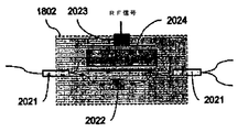
図1を参照すると、2つのセンサ110及び120を含むセンサシステムは、投影レンズ(PO)部品150内のレンズ140のフレーム素子130の位置をモニタするように配設されている。センサ110及び120は、PO部品150内に埋設され、それぞれ、フレーム素子112及び122に装着されている。センサシステムは、光源と、検出器と、信号処理電子品とを含む光源/検出器(SDユニット)ユニットSDユニット160も含む。SDユニット160は、それぞれ、光ファイバ111及び121を介してセンサ110及び120に、他の光ファイバを介して他のセンサに接続されている。動作中、SDユニット160は、ファイバ111及び121を介して、光源(例えば、レーザ又はLED)からの光をセンサ110及び120に方向づける。ファイバ111及び121は、また、それぞれ、センサ110及び120からの光をSDユニット160内の1つ又はそれ以上の検出器に送出する。
Like reference symbols in the various drawings indicate like elements.
Referring to FIG. 1, a sensor system including two
SDユニット160は、また、サーボ制御装置170と通信しており、サーボ制御装置170は、信号をPO部品150内のアクチュエータ(例えば、圧電アクチュエータ)に送り、アクチュエータは、SDユニット160からの信号に応答して、PO部品内のレンズ140及び他の構成部品の位置を調整するように構成されている。
The
センサ
図2を参照すると、センサ110は、反射光学目標210及び出力結合器220を含む。光学目標210は、フレーム素子130に装着され、出力結合器220は、フレーム素子130に対する動きが可能であるフレーム素子112に装着されている。
Sensor Referring to FIG. 2,
一般に、受動光センサは、センサに送出された光を測定波面及び基準波面に分割する干渉計である。試験波面は、光学目標210に方向づけられて干渉計に反射する。基準波面は、基準面から反射する。干渉計は、反射測定波面及び基準波面を再合成し、再合成された光は、その後、光ファイバに方向づけられる。合成波面同士が干渉して、2つの波面間の光路差(OPD)に関する情報を含む干渉図が生成される。センサシステムは、この情報を使用して、受動光センサに対する光学目標の位置を判断する。
In general, a passive optical sensor is an interferometer that divides light transmitted to the sensor into a measurement wavefront and a reference wavefront. The test wavefront is directed to the
光学目標の位置に関する特定の情報は、変化する可能性がある。一部の実施形態においては、受動光センサと光学目標との間の位置の相対的変化を判断するだけで十分であり、その場合、この情報は、各センサから受光された干渉光内の強度変動に対応する干渉信号の位相の変化をモニタすることにより判断することができる。特定の実施形態においては、予め確立された基準フレーム内の光学目標の絶対位置が望まれる。様々な方法を用いてこの情報を判断することができる。このような方法は、例えば、L.L.Deck著フーリエ変換位相ずれ干渉分光法、Applied Optics(応用光学)、第42巻、第13号(2003年5月)、及び、C.E.Towersら共著多重波長干渉分光法における全視野縞位相分析用時間効率中国の剰余定理アルゴリズム Optics Express、第12巻、第6号(2004年3月)において開示されている。
The specific information regarding the position of the optical target can vary. In some embodiments, it is sufficient to determine the relative change in position between the passive light sensor and the optical target, in which case this information is the intensity in the interfering light received from each sensor. This can be determined by monitoring the change in the phase of the interference signal corresponding to the fluctuation. In certain embodiments, the absolute position of the optical target within a pre-established reference frame is desired. Various methods can be used to determine this information. Such a method is described, for example, in L.L. L. Deck, Fourier transform phase-shifting interferometry , Applied Optics (Applied Optics), Vol. 42, No. 13 (May 2003), and C.I. E. Times for full-field fringe phase analysis in Multiple Wavelength Interference Spectroscopy co-authored by Towers et al., Chinese Remainder Theorem Algorithm Optics Express,
一般に、センサシステムは、可視波長又は赤外線波長など、様々な波長にて動作するように構成することができる。一部の実施形態においては、センサシステムは、電気通信業界で一般的に使用されている1つ又はそれ以上の波長にて(例えば、約900nmから約1,600nmの範囲で)動作する。 In general, sensor systems can be configured to operate at various wavelengths, such as visible wavelengths or infrared wavelengths. In some embodiments, the sensor system operates at one or more wavelengths commonly used in the telecommunications industry (eg, in the range of about 900 nm to about 1,600 nm).
センサは、相対的に低電力のセンサとすることができる。例えば、各センサでの放射電力(例えば、センサ端部にて各ファイバを出る放射電力)は、約10mW以下(例えば、約5mW以下、約4mW以下、約3mW以下、約2mW以下、約1mW以下、約0.5mW以下、約0.1mW以下)とすることができる。 The sensor can be a relatively low power sensor. For example, the radiated power at each sensor (for example, the radiated power exiting each fiber at the sensor end) is about 10 mW or less (for example, about 5 mW or less, about 4 mW or less, about 3 mW or less, about 2 mW or less, about 1 mW or less) , About 0.5 mW or less, about 0.1 mW or less).
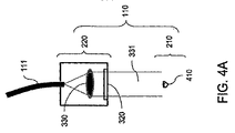
一般に、センサ110及び120の構成は、変化する場合がある。図3を参照すると、一部の実施形態においては、目標210は、逆反射体310を含み、受動光センサ220は、透過基準平面320(例えば、ガラス平面)及び視準レンズ330を含む。視準レンズ330は、ファイバ111からの発散光を視準して透過基準平面320を照射する。光の一部は、透過基準平面320により反射されて、レンズ330によりファイバ111端部上に集光される。ビーム331により示す光の一部は、透過基準平面330により透過されて逆反射体310を照射する。逆反射体310は、光を受動光センサ220に向かって光を反射する。この光は、少なくともある程度、透過基準平面320により透過され、レンズ330により、ファイバ111端部に集光される。逆反射体310から反射した波面は、透過基準平面320から反射した波面と干渉する。結果的に生じる干渉の位相は、SDユニット160にてモニタすることができ、受動光センサ220に対する逆反射体310の相対位置に関する情報が得られる。
In general, the configuration of
図4Aを参照すると、一部の実施形態においては、目標光学品のサイズは、受動光センサ220からの照射ビームの横断面寸法より小さいとすることができる。一例として、逆反射体410は、ビーム331より実質的に小さい。このタイプの構成は、照射の種々の特性が、目標光学品が原位置から移動するときに目標光学品に対して名目上一定であるという点で有利であると考えられる。これにより、特定の所望の雑音レベルを達成するために必要な逆反射体波面品質に関する諸要件を軽減することができる。更に、このタイプの構成は、それでも高次の干渉影響の誤差を相対的に小さく保ちながら干渉コントラストを向上させることを可能にすることができる。
With reference to FIG. 4A, in some embodiments, the size of the target optics can be smaller than the cross-sectional dimension of the illumination beam from the passive
一般に、目標反射体のサイズに対するビーム横断面寸法は、変化する可能性がある。一部の実施形態においては、ビーム横断面寸法(例えば、直径)は、目標反射体のサイズと比較すると相対的に小さいとすることができる。例えば、ビーム横断面寸法(少なくとも1つの方向において)は、約0.2以下(例えば、約0.1以下、約0.05以下、約0.01以下)×目標反射体のサイズである。 In general, the beam cross-sectional dimension relative to the size of the target reflector can vary. In some embodiments, the beam cross-sectional dimension (eg, diameter) can be relatively small compared to the size of the target reflector. For example, the beam cross-sectional dimension (in at least one direction) is about 0.2 or less (eg, about 0.1 or less, about 0.05 or less, about 0.01 or less) × the size of the target reflector.
特定の実施形態においては、ビームは、ビームが目標と接触する場合、相対的に小さい横断面寸法を有することができる。例えば、少なくとも1つの方向におけるビーム横断面寸法(例えば、直径)は、約0.5mm以下(例えば、約0.3mm以下、約0.2mm以下、約0.1mm以下、約0.05mm以下、約0.04mm以下、約0.03mm以下、約0.02mm以下、約0.01mm以下)とすることができる。一部の実施形態においては、少なくとも1つの方向におけるビームの横断面寸法(例えば、直径)は、約100λ以下(例えば、約90λ以下、約80λ以下、約70λ以下、約60λ以下、約50λ以下、約40λ以下、約30λ以下、約20λ以下)とすることができる。ここで、λは、ビームの波長である。 In certain embodiments, the beam can have a relatively small cross-sectional dimension when the beam contacts the target. For example, the beam cross-sectional dimension (eg, diameter) in at least one direction is about 0.5 mm or less (eg, about 0.3 mm or less, about 0.2 mm or less, about 0.1 mm or less, about 0.05 mm or less, About 0.04 mm or less, about 0.03 mm or less, about 0.02 mm or less, or about 0.01 mm or less). In some embodiments, the cross-sectional dimension (eg, diameter) of the beam in at least one direction is about 100λ or less (eg, about 90λ or less, about 80λ or less, about 70λ or less, about 60λ or less, about 50λ or less. About 40λ or less, about 30λ or less, or about 20λ or less). Here, λ is the wavelength of the beam.
ビーム伝播方向に対して半径方向に対称形であるガウス強度プロファイルを有するビームについては、横断面寸法は、ビーム強度がピーク値の1/eを有するところで測定される。 For a beam with a Gaussian intensity profile that is radially symmetric with respect to the beam propagation direction, the cross-sectional dimension is measured where the beam intensity has 1 / e of the peak value.
図4Bを参照すると、相対的に小さい横断面寸法を有するビームを利用するセンサ構成の例は、センサ2100であり、センサ2100は、ビームを平面鏡目標2130に方向づける。センサ2100は、透過基準平面2120(例えば、ガラス平面)及び集光レンズ2110を含む。集光レンズ2110は、ファイバ2101からの発散光を回収して、基準平面2120を介して光を目標2130に方向づける。光の一部は、基準平面2120の表面により反射されて、ファイバ2101端部上にレンズ2110により集光される。光の一部は、基準平面2120により透過されて基準平面2120を照射する。基準平面2120は、光を基準平面2120と、レンズ2110と、ファイバ2101とに向かって反射する。この光は、少なくともある程度、基準平面2120により透過され、レンズ2110により集光されて、ファイバ2101に結合される。目標2130から反射した波面は、透過基準平面2120の表面から反射した波面と干渉する。結果的に生じる干渉の位相は、上述した実施形態の場合と同様にモニタされ、基準平面2120に対する鏡2130の相対位置に関する情報が得られる。
Referring to FIG. 4B, an example of a sensor configuration that utilizes a beam with a relatively small cross-sectional dimension is
一部の実施形態においては、鏡目標2130は、光ビーム腰部に随意的に位置決めされる。このような構成により、鏡目標の転倒及び傾動に関連した位相誤差に対するセンサの感度を軽減することができる。特定の実施形態においては、光ビーム腰部に鏡目標2130を位置決めすることは、鏡目標が転倒及び/又は傾動したときに光ファイバ内に反射したビームの結合効率が低減される量を軽減することができる。更に、光ビームが狭い腰部(例えば、直径が約100μm以下の腰部、約60μm以下、約50μm以下、約40μm以下、約30μm以下など)を有する場合、鏡の転倒/傾動による結合効率損失は、更に低減することができる。一部の実施形態においては、公称位置から0.2度以下(例えば、0.1度以下)の鏡の方位の変化(例えば、転倒又は傾動によって)があると、結果的に、公称位置での結合効率の50%に劣らないほど(例えば、約60%以上、約70%以上、約80%以上、約90%以上)までの結合効率の低減が発生する可能性がある。ここでは、公称位置とは、光ファイバへの光ビームの結合効率が最大値である鏡の位置を指す。
In some embodiments, the
目標にて相対的に小さい横断面寸法を有するビームを利用する実施形態は、相対的にコンパクトとすることができる。例えば、ファイバ2101端部から鏡2130までの距離は、約10mm以下(例えば、約5mm以下、約3mm以下、約2mm以下、約1.5mm以下、約1mm以下)とすることができる。
Embodiments that utilize beams with relatively small cross-sectional dimensions at the target can be relatively compact. For example, the distance from the end of the
図4Cは、目標において相対的に小さい横断面寸法を有するビームを利用するセンサの別の例を示す。具体的には、図4Cは、レンズ2110を介してファイバ2101からの放射を目標鏡2130に方向づけるように構成されたセンサ2200を示す。図4Bに示すセンサ2100とセンサ2200との相違点は、センサ2200は、レンズ2110から集光した光を目標2130に方向づける基準平面2120ではなくて、プリズム2220を有するという点である。ここでは、基準面は、プリズム2220の表面2211である。センサ2200は、センサが設置されるべき構造体がライン内ビーム路をセンサ2100においてのようには使用することはできない用途において使用することができる。特定の実施形態においては、更なる光学部品を使用して必要に応じてビーム路を更にねじることができる。
FIG. 4C shows another example of a sensor that utilizes a beam having a relatively small cross-sectional dimension at the target. Specifically, FIG. 4C shows
一部の実施形態においては、集光レンズの機能性を実現するとともに基準面を実現する構成部品を使用することができる。例えば、図4Dを参照すると、センサ2300は、基準面の役目をする平面2311を有するレンズ2310を含むことができる。このようなレンズの例としては、平面凸レンズ及び勾配屈折率材料から形成されたレンズ(GRINレンズ)がある。一部の実施形態においては、電気通信用途での使用に設計されたGRINレンズを使用することができる。
In some embodiments, components that implement the functionality of the condenser lens and implement the reference plane can be used. For example, referring to FIG. 4D, the
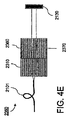
図4Eは、レンズ2310に加えてビーム分割器キューブ2370を含むセンサ2350の別の実施形態を示す。ビーム分割器キューブ2370の表面2360は、センサ2350用基準面となる。
FIG. 4E shows another embodiment of a
他の構成も可能である。例えば、図5を参照すると、一部の実施形態においては、センサは、光が目標に複光路を成すように構成することができる。この例においては、受動光センサは、鏡520を含み、逆反射体510は、第1のパスで、受動光センサからの照射が鏡520に向かって方向づけられるようにサイズ決定されている。鏡520は、光を逆反射体510に反射し、逆反射体510は、光を透過基準平面320及びレンズ330に方向づける。
Other configurations are possible. For example, referring to FIG. 5, in some embodiments, the sensor can be configured such that the light has a double light path to the target. In this example, the passive light sensor includes a
複光路は、逆反射体が単独に使用されて逆行運動(retro motion)に対する感度を増大させる場合に発生するビーム反転の影響を補正することができる。
目標逆反射体510を適当に取り付けると、逆反射体510を介して光路の熱依存を補正することができる。例えば、逆反射体510は、熱膨張率が、マウントの熱膨張が、例えば、センサ内の光学部品の屈折率の熱誘発変化及び/又はセンサの熱誘発物理的経路長変化からのセンサの熱誘発OPD変化を補償するようなものである材料から製造されたマウント512内に取り付けることができる。
The double optical path can correct for the effects of beam reversal that occurs when a retroreflector is used alone to increase the sensitivity to retro motion.
When the target retroreflector 510 is appropriately attached, the heat dependence of the optical path can be corrected via the retroreflector 510. For example, the retroreflector 510 may have a coefficient of thermal expansion, the thermal expansion of the mount, for example, the heat of the sensor from a heat-induced change in refractive index of optical components in the sensor and / or a heat-induced physical path length change in the sensor. It can be mounted in a mount 512 made from a material that is such as to compensate for induced OPD changes.
一部の実施形態においては、センサは、遠隔基準面を含むことができる。例えば、図6を参照すると、一部の実施形態においては、ファイバ結合器/分割器620は、センサ110に加えて遠隔基準鏡610に光を方向づける。遠隔基準を使用すると、名目上のスタンドオフを異なる長さに設定することができる。遠隔基準を使用することは、センサ光学品内での熱影響を補償することを可能にすることができる。例えば、一部の実施形態においては、ファイバピッグテールを使用してセンサOPD全体を改変するとともに、及び/又はピッグテールの熱OPD変動(例えば、センサ内の光学部品の屈折率の熱誘発変化及び/又はセンサ内の熱誘発物理的経路長変化による)を使用して、主要センサ空洞共振器内のガラス又は他の光学材料からの同様の影響を補償することができる。
In some embodiments, the sensor can include a remote reference plane. For example, referring to FIG. 6, in some embodiments, fiber coupler / splitter 620 directs light to
一般に、センサシステムは、偏光又は非偏光を利用することができる。図7を参照すると、偏光を使用するセンサの例が示されている。この例においては、受動光センサ220は、偏光ビーム分割器720と、基準鏡720と、逆反射体724と、1/4波板726及び728とを含む。目標光学品210は、平面鏡710を含む。この構成は、高安定平面鏡干渉分光法(HSPMI)に対応する。入力ビームは、第1の視準レンズ730を介してHSPMIに結合される。出力ビームは、第2のレンズ732を介して異なるファイバに結合される。
In general, sensor systems can utilize polarized or unpolarized light. Referring to FIG. 7, an example of a sensor that uses polarized light is shown. In this example, passive
図8を参照すると、一部の実施形態においては、ファイバ111の端面810は、センサ110の基準面となるように使用することができる。ここでは、センサ110は、平面鏡目標830、及び、ファイバ111から放出された光を目標830での又は目標830近傍の地点に集光し、また、目標830から反射した光をファイバ111端部に集光するレンズ820を含む。
Referring to FIG. 8, in some embodiments, the
先の種々の実施形態においては、逆反射体又は平面鏡が目標光学品として使用されるが、他の光学部品をこの目的に使用することもできる。例えば、図9を参照すると、一部の実施形態においては、非平面反射体910を目標光学品として使用することができる。このような目標のほうが、受動光センサ220と目標との間の芯狂いに強いと考えられる。
In the various previous embodiments, a retroreflector or plane mirror is used as the target optics, but other optical components can be used for this purpose. For example, referring to FIG. 9, in some embodiments, a
別の例として、また、図10を参照すると、一部の実施形態においては、猫の目タイプの逆反射体1001を目標光学品に使用することができる。猫の目逆反射体1001は、レンズ1010(例えば、球面レンズ)及び鏡1020(例えば、平面鏡又は曲面鏡)を含む。入射光は、レンズ1010により鏡1020上に集光されて、鏡1020によりレンズ1010に反射される。反射光は、レンズ1010を介して逆経路を辿って、受動光センサ220に戻る。猫の目逆反射体を使用する種々の構成は、他の構成に対して角変形誤差の許容範囲の増強を行なうことができる。
As another example, and referring to FIG. 10, in some embodiments, a cat's
図11を参照すると、光が目標光学品に複光路を成すセンサの別の例が示されている。この実施形態においては、受動光センサ220は、レンズ330及び透過光平面320に加えて逆反射体1110を含む。この場合の目標は、光ファイバ111から逆反射体1110に向かって光を反射する向きにある平面鏡1120である。
Referring to FIG. 11, another example of a sensor in which light forms a double optical path to a target optical product is shown. In this embodiment, passive
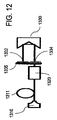
図12及び図13を参照すると、センサの更なる例が示されている。この例においては、センサは、応力除去素子1330によりファイバ視準器1320に装着されている光ファイバ1311を介してSDユニット1310から光を受光するように配設されている。ファイバ視準器1320は、ファイバからの光を逆反射体1330に方向づけるように位置決めされている。ウィンドウ1335は、ファイバ視準器1320と逆反射体1335との間に位置決めされている。ファイバ視準器1320もウィンドウ1335も、取付け板1340に取り付けられている。このセンサにおける光学目標である逆反射体1330は、
取付け板1340から遠いところに取り付けられている。ウィンドウ1335の表面の半分は、非偏光ビーム分割器塗膜1334が被覆されており、他方の半分は、反射塗膜1332(例えば、可視光を対象とした銀又はアルミニウム)が被覆されている。ファイバ視準器1320から放出された光は、初めに、非偏光ビーム分割器塗膜1334が被覆されたウィンドウ表面の部分に当たる。この光の一部は、ウィンドウにより逆反射体1330に向かって透過され、一方、一部は、ファイバ視準器1220に向かって反射されて、試験波面が実現される。透過部分は、逆反射体1330により反射されて反射塗膜1332に当たる。被膜から反射して同じ経路に沿ってファイバ視準器1320に戻って、測定波面が実現される。
Referring to FIGS. 12 and 13, a further example of a sensor is shown. In this example, the sensor is arranged to receive light from the
It is mounted at a location far from the mounting
一般に、先に論じたように、センサシステムにおける光源/検出器ユニット(SDユニット)は、実際のセンサ自体より遠いところにある。特定の実施形態においては、SDユニットとセンサとの間の情報導管のみが、光ファイバである。センサが受動式(例えば、センサが電気回路を含まない)である実施形態においては、SDユニットをセンサに接続するために必要である電線はない。 In general, as discussed above, the light source / detector unit (SD unit) in the sensor system is further away than the actual sensor itself. In certain embodiments, only the information conduit between the SD unit and the sensor is an optical fiber. In embodiments where the sensor is passive (eg, the sensor does not include an electrical circuit), there are no wires needed to connect the SD unit to the sensor.
センサシステムアーキテクチャ及び測定法
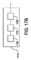
一般に、様々な異なるセンサシステムアーキテクチャが可能である。システムアーキテクチャは、通常、光学部品位置をモニタするために採用される測定技術など、様々な要因、ならびに、コストなどの他の要因に基づいて選択される。一部の実施形態においては、多重化構成を使用することができる。一般に、多重化構成とは、複数のセンサからの信号が共通の伝送路(例えば、光ファイバ)で搬送される構成を指す。例えば、図14Aを参照すると、SDユニット1410は、4つのセンサ1420の1つに直に、他の3つのセンサに間接的に接続されている。換言すると、センサは、SDユニット1410に直列に接続されている。光は、SDユニット1410からセンサ1420まで共通の光ファイバにより行き来する。センサ1420は、PO部品1410部品内に埋設されており、一方、SDユニット1410は、PO部品から遠いところにある。センサシステムは、波長計1430を含むこともでき、波長計1430は、SDユニット1410に接続されている。
Sensor System Architecture and Measurement Methods In general, a variety of different sensor system architectures are possible. The system architecture is typically selected based on various factors, such as the measurement technique employed to monitor the optical component position, as well as other factors such as cost. In some embodiments, a multiplexing configuration can be used. In general, a multiplexed configuration refers to a configuration in which signals from a plurality of sensors are carried by a common transmission path (for example, an optical fiber). For example, referring to FIG. 14A, the
多重化は、様々な異なる方法で達成することができる。例えば、一部の実施形態においては、周波数符号化を用いることができる。各センサは、異なるセンサのOPDが名目上異なるように構成することができる。したがって、各センサの信号は、波長同調が採用された場合には他のセンサの信号と異なる周波数を有することになる。信号に周波数分析を行うと、異なるセンサからの信号を区別することができる。 Multiplexing can be accomplished in a variety of different ways. For example, in some embodiments, frequency encoding can be used. Each sensor can be configured so that the OPDs of the different sensors are nominally different. Therefore, the signal of each sensor has a different frequency from the signals of other sensors when wavelength tuning is employed. When frequency analysis is performed on the signals, signals from different sensors can be distinguished.
あるいは、又は、更に、波長分割を多重化に用いることができる。例えば、様々な異なる波長での光をセンサに送出することができる。各センサは、他のフィルタと異なる波長又は波長帯域を渡す波長フィルタを含む。このようにして、各センサの信号は、戻り信号内の適当な波長符号を見ることにより区別することができる。 Alternatively or additionally, wavelength division can be used for multiplexing. For example, light at a variety of different wavelengths can be sent to the sensor. Each sensor includes a wavelength filter that passes a different wavelength or wavelength band than the other filters. In this way, the signal of each sensor can be distinguished by looking at the appropriate wavelength code in the return signal.
一部の実施形態においては、光は、分散ネットワークを使用してセンサに分配されるか、及び/又はセンサから回収される。図14Cを参照すると、分散ネットワークの例は、3つのポート(例えば、1つの入力ポート及び2つの出力ポート又は2つの入力ポート及び1つの出力ポート、それぞれ、結合器が分割器の役目を務めるか、又は、結合器の役目を務めるかによる)を有する幾つかの光ファイバ結合器1452を含む。ネットワークの最終段階にて、出力結合器1453は、循環器、又は、1つのポートが未使用のままである標準的な2×2結合器である。また、図14Cのネットワークにおいて、検出器1450も示されており、検出器1450は、センサから光信号を受信する。原則的に、ネットワークは、特定の実行例によっては、任意の数のセンサから信号を送出及び/又は回収するために使用することができる。一部の実施形態においては、システムは、10個以上のセンサ(例えば、12個以上のセンサ、15個以上のセンサ、18個以上のセンサ、20個以上のセンサ、21個以上のセンサ、25個以上のセンサ、30個以上のセンサ、32個以上のセンサ、35個以上のセンサ)を含むように構成することができる。
In some embodiments, light is distributed to and / or recovered from sensors using a distributed network. Referring to FIG. 14C, a distributed network example has three ports (eg, one input port and two output ports or two input ports and one output port, respectively, where the combiner acts as a divider). Or a number of fiber optic couplers 1452 (depending on whether they act as couplers). At the end of the network, the
一部の実施形態においては、ネットワーク内の最終ステージ分割器は、循環器と置き換えることができる。このような構成により、所望であれば、4倍の光学的効率上昇を得ることができる。 In some embodiments, the final stage divider in the network can be replaced with a circulator. With such a configuration, a fourfold increase in optical efficiency can be obtained if desired.
特定の実施形態においては、コヒーレンス符号化を多重化に用いることができる。コヒーレンス符号化では、一般的に、広帯域光源を使用して各センサに独自の重なり合いなしのOPDを供給する。各センサは、その後、測定OPDにより特定することができる。例えば、各センサは、異なる名目上のOPDを有することができ、照射パルスを使用してOPDを測定することができる。特定の光学距離により分離された2面空洞共振器を含むセンサに方向づけられる2つの時間分離パルスを検討されたい。パルス時間分離が、パルスが空洞共振器を横行する往復時間に等しい場合、2つの別個のパルスは、干渉することがある可能性がある。それで、パルスの周波数を変えることにより、干渉を生成する周波数を捜すことにより空洞共振器長を推論することができる。このようにして、SDユニットは、異なるセンサからの信号を特定することができる。 In certain embodiments, coherence coding can be used for multiplexing. Coherence encoding typically uses a broadband light source to provide each sensor with its own non-overlapping OPD. Each sensor can then be identified by a measurement OPD. For example, each sensor can have a different nominal OPD, and an irradiation pulse can be used to measure OPD. Consider two time-separated pulses that are directed to a sensor that includes a two-sided cavity resonator separated by a specific optical distance. If the pulse time separation is equal to the round trip time that the pulse traverses the cavity, two separate pulses can interfere. Thus, by changing the frequency of the pulse, the cavity length can be inferred by looking for the frequency that produces the interference. In this way, the SD unit can identify signals from different sensors.
コヒーレンス符号化は、結合空洞共振器干渉分光法を用いて実現することもできる。結合空洞共振器干渉分光法においては、走査することができる別の空洞共振器からの広帯域光で空洞共振器を照射することにより空洞共振器に問い合わせが行われる。これは、センサ空洞共振器のOPDが固定のままである間に走査を可能にすることができる。 Coherence encoding can also be achieved using coupled cavity resonator interferometry. In coupled cavity interferometry, the cavity is interrogated by illuminating the cavity with broadband light from another cavity that can be scanned. This can allow scanning while the sensor cavity resonator OPD remains fixed.
一部の実施形態においては、各センサは、独自のファイバによりSDユニットに接続されており、光を各センサに送出するために共通の光源が使用される(例えば、図14Bを参照されたい)。例えば、図14Bを参照すると、センサ1420は、SDユニット1410に並列に接続されている。換言すると、各センサは、それぞれの光ファイバを介してSDユニット1410に直に接続されている。
In some embodiments, each sensor is connected to the SD unit by its own fiber, and a common light source is used to send light to each sensor (see, eg, FIG. 14B). . For example, referring to FIG. 14B, the
一部の実施形態においては、走査白色光干渉分光法を用いることができる。例えば、各センサにおいては、基準面(例えば、結合空洞共振器内の遠隔基準面)を干渉が観察されるまで移動させることができる。 In some embodiments, scanning white light interferometry can be used. For example, in each sensor, a reference plane (eg, a remote reference plane in the coupled cavity) can be moved until interference is observed.
特定の実施形態においては、光周波数が異なり、かつ、対向する偏光を有する2つのビームに干渉計の試験又は基準脚部を別個に横行させる偏光符号化を用いることができる。戻り時に、ビームは、干渉させ(例えば、偏光器を介して)、干渉の周波数(2つの光周波数間の差に等しい)を測定する。脚部の一方が他方に対して移動中である場合、その光は、ドプラ偏移されて、干渉周波数が変化する。 In certain embodiments, polarization encoding can be used that causes two beams with different optical frequencies and opposite polarizations to traverse the interferometer test or reference leg separately. On return, the beam interferes (eg, via a polarizer) and measures the frequency of interference (equal to the difference between the two optical frequencies). When one of the legs is moving relative to the other, the light is Doppler shifted and the interference frequency changes.
一部の実施形態においては、多重波長干渉分光法が用いられる。例えば、センサ空洞共振器は、幾つかのよく知られている、離散的な波長で照射する(順次、又は同時に)ことができ、信号位相偏移を波長の関数として判断する。位相偏移は、幾つかの方法で、例えば、離散波長の各々を位相偏移することにより求めることができる。あるいは、又は、更に、各波長にて干渉強度を測定して、その後、本システムの物理モデルで、強度と波長の最良の適合を介して空洞共振器長を判断することができる。 In some embodiments, multiple wavelength interferometry is used. For example, sensor cavity resonators can be illuminated (sequentially or simultaneously) at several well-known discrete wavelengths, and determine the signal phase shift as a function of wavelength. The phase shift can be determined in several ways, for example by phase shifting each of the discrete wavelengths. Alternatively or additionally, the interference intensity can be measured at each wavelength, and then the cavity model can be determined in the physical model of the system through the best fit of intensity and wavelength.
特定の実施形態においては、周波数同調を用いることができる。周波数同調は、上記したL.L.Deck著フーリエ変換位相偏移干渉分光法、Applied Optics、第42巻、第13号(2003年5月)で説明されている。長い十分な範囲にわたって波長を連続的に位相同調することができる場合、干渉のフーリエ分析又は物理モデルに適合する最小2乗法により空洞共振器長を求めることができる。 In certain embodiments, frequency tuning can be used. Frequency tuning is the same as that described in L. L. Decks, Fourier Transform Phase Shifted Interferometry , Applied Optics, Vol. 42, No. 13 (May 2003). If the wavelength can be continuously phase tuned over a long enough range, the cavity length can be determined by Fourier analysis of interference or a least squares method that fits the physical model.
システムは、掃引波長干渉分光法、結合空洞共振器干渉分光法、コヒーレンス走査干渉分光法、ヘテロダイン干渉分光法、及び/又は多重波長干渉分光法などの1つ又はそれ以上の基本的な干渉分光技術に基づくことができる。例示的なシステムを以下で説明する。 The system includes one or more basic interferometry techniques such as swept wavelength interferometry, coupled cavity interferometry, coherence scanning interferometry, heterodyne interferometry, and / or multiwavelength interferometry. Can be based on. An exemplary system is described below.
(A)結合空洞共振器によるコヒーレンス走査干渉分光法
コヒーレンス走査干渉分光法では、相対的に短いコヒーレンス長を有する光源(例えば、帯域幅光源)を利用する。したがって、干渉縞は、ゼロにて又はゼロ近傍にてOPDについてのみ検出される。従来のレーザ干渉分光法における周期的な曖昧さを排除するために干渉位置推定を利用して、絶対OPD測定にコヒーレンス走査干渉分光法を用いることができる。センサが受動式であることから、OPDは、結合空洞共振器構成部を介して間接的に走査される。
(A) Coherence scanning interferometry with coupled cavity resonators Coherence scanning interferometry uses a light source (eg, a bandwidth light source) having a relatively short coherence length. Accordingly, interference fringes are detected only for OPD at or near zero. Coherence scanning interferometry can be used for absolute OPD measurements using interference position estimation to eliminate periodic ambiguity in conventional laser interferometry. Because the sensor is passive, the OPD is scanned indirectly through the coupled cavity resonator component.
結合空洞共振器外形形状を用いることは、他の方法に対して、複雑性増大及び縞コントラスト低減を犠牲にしながらも遠隔走査を可能にすることができ、光源コヒーレンス特性が試験空洞共振器OPD範囲に結び付けられる。図15を参照すると、一般に、結合空洞共振器構成部は、走査空洞共振器1510及びセンサ空洞共振器1520を含む。走査空洞共振器1510は、2つの経路Ll及びL2を含み、少なくともその一方は、可変である。センサ空洞共振器1520は、2つの経路L3及びL4を含む。したがって、各空洞共振器から2つの脚部の組み合わせに対応する信号1521を入力信号1511が出る可能な経路が4つある(L1+L3、L1+L4、L2+L3、L2+L4)。
Using a coupled cavity geometry can enable remote scanning at the expense of increased complexity and reduced fringe contrast, compared to other methods, and the source coherence characteristics are within the test cavity resonator OPD range. Tied to Referring to FIG. 15, the coupled cavity resonator component generally includes a
確実に、不要な経路組み合わせからの干渉が、当該の空洞共振器からの干渉に影響を与えないようにするために、経路間のOPDは、光のコヒーレンス長より大きいものであるべきである。換言すると、センサ空洞共振器のOPDは、光源コヒーレンス長より大きいものであるべきであり、これにより、センサ隙間が大きくなる傾向がある。 To ensure that interference from unwanted path combinations does not affect interference from the cavity, the OPD between paths should be greater than the optical coherence length. In other words, the sensor cavity resonator OPD should be greater than the source coherence length, which tends to increase the sensor gap.
図16を参照すると、結合空洞共振器を有するコヒーレンス走査干渉分光法システム1600が示されている。システム1600は、光ファイバを介してセンサ1620と接続されたSDユニット1610を特徴とする。SDユニット1610は、光ファイバ結合器1615と、検出器1618と、基準空洞共振器1640とを含む。更に、SDユニット1610は、結合空洞共振器内の可変OPDを実現するOPD偏移器1630、及び、広帯域超発光ダイオード(SLED)など、低コヒーレンス光源1612を含む。適切な電力及び広帯域幅を有するSLEDは、例えば、EM4社(マサチューセッツ州ベッドフォード)、Covega(メリーランド州ジェサップ)、DenseLight Semiconductors(シンガポール)から販売されている。一部の実施形態においては、光源は、1550nmに中心がある60nmガウススペクトル幅(半値全幅、FWHM)を実現する。このような光源は、20μm幅(FWHM)でコヒーレンス関数を生成する。
Referring to FIG. 16, a coherence
周波数領域分析を用いて、データを分析することができる。周波数領域分析法は、例えば、P.de Groot及びL.Deck著「空間周波数領域における白色光干渉分光法分析による表面形状測定」、最新光学品学会誌(Journal of Modern Optics)42:389ページから401ページ(1995年)で開示されており、この内容全体は、参照により本明細書に組み込まれる。一部の実施形態においては、単一4096点高速フーリエ変換(FFT)の計算を介してデータの線形走査を分析することができ、この演算は、高速デジタル信号プロセッサ及び/又はプログラマブル論理回路で、約0.25msで完了することができる。したがって、結果は、その後の測定の前に出力することができるが、データ経年変化は、分析時間及び空洞共振器OPDに左右されることになる。走査が非線形(ただし公知)である場合、より複雑な分析を行なうことができる。 Data can be analyzed using frequency domain analysis. The frequency domain analysis method is, for example, P.I. de Groot and L.L. Decks, “Surface shape measurement by white light interferometry analysis in spatial frequency domain”, Journal of Modern Optics 42: 389-401 (1995), the entire contents Are incorporated herein by reference. In some embodiments, a linear scan of the data can be analyzed via a single 4096 point Fast Fourier Transform (FFT) calculation, which can be performed with a high speed digital signal processor and / or programmable logic circuitry, It can be completed in about 0.25 ms. Thus, the results can be output before subsequent measurements, but the data aging will depend on the analysis time and the cavity resonator OPD. More complex analysis can be performed if the scan is non-linear (but known).
(B)結合空洞共振器及びヘテロダイン干渉分光法によるコヒーレンス走査干渉分光法
結合空洞共振器及びヘテロダイン干渉分光法を用いたコヒーレンス走査干渉分光法では、測定は、2つのモードに分割される。相対的に遅いコヒーレンス走査を用いて、全てのセンサについて同時に空洞共振器絶対OPDを見つけ(「絶対モード」という)、迅速なヘテロダイン法を用いて、その時点からOPDの変動を追跡する(「相対モード」という)。図17Aを参照すると、システム1700は、SDユニット1710及びセンサ1720を含む。SDユニット1710は、光ファイバ結合器1715と、検出器1718と、基準空洞共振器1740とを含む。更に、SDユニット1710は、低コヒーレンス光源1712と、準狭帯域光源1714と、OPD偏移器1718と、周波数変調器1716とを含む。OPD偏移器1718は、光源1712とセンサ1720に接続するネットワークとの間に位置決めされた結合空洞共振器の1つの脚部内に設置されている。周波数変調器は、光源1714と、センサ1720と接続するネットワークとの間に位置決めされた第2の結合空洞共振器の1つの脚部内に設置されている。
(B) Coherence scanning interferometry using coupled cavity and heterodyne interferometry In coherence scanning interferometry using coupled cavity and heterodyne interferometry, the measurement is divided into two modes. A relatively slow coherence scan is used to find the cavity resonator absolute OPD for all sensors simultaneously (referred to as “absolute mode”), and a rapid heterodyne method is used to track OPD variation from that point in time (“relative” Mode "). Referring to FIG. 17A,
動作中、低コヒーレンス光源1712は、絶対モードに使用される。このモードは、各センサの絶対OPDを同時に取得するために起動時に1回行なう(又は、必要に応じて)ことができる。その測定の速度は、相対的に遅いもの(例えば、数秒)とすることができるので、センサOPDはこの時間中には変化しないと想定することができる。走査速度を除き、手順及び分析は、小区分Aに関して上述したものと類似のものである。絶対モードと相対モードとの間で大きく縞次数が変化しないようにセンサが十分に安定したものである限り、2つの測定結果を結合して、サブnmの精度まで絶対センサOPDを判断することができる。
In operation, the low
相対モードにおいては、準狭帯域光源1714が使用される。この光源のコヒーレンス長は、センサOPDの全範囲にわたって堅牢な干渉を観察するほどの十分な長さであるが、結合空洞共振器システムに付随する余分な空洞共振器干渉を排除するほどに十分に短いものであるべきである。適切なコヒーレンス形状を有する光源は、所望であれば、所要の強度を回復する増幅器と共に、SLED及びフィルタを使用して構成することができる。図17Bを参照すると、例示的な準狭帯域光源は、広帯域光源1750(例えば、SLED)と、インライン光ファイバ帯域通過フィルタ1755(例えば、1nmの帯域通過幅を有する)と、帯域通過フィルタを出る信号を増幅する半導体光増幅器(SOA)1760とを含む。
In the relative mode, a quasi narrow
ヘテロダインモードについては、狭帯域光をセンサに供給する結合空洞共振器は、周波数変調器1716を含む。周波数変調器1716は、ヘテロダイン周波数を生成するために、空洞共振器脚部の少なくとも1つの中を進む光の光周波数を変える。その後、位相測定結果を、例えば、米国特許第5,249,030号明細書で説明されている種々の方法と類似の方法で判断することができ、この特許の内容全体は、参照により本明細書に組み込まれる。
For the heterodyne mode, the coupled cavity that provides narrowband light to the sensor includes a
(C)多重波長干渉分光法及びヘテロダイン干渉分光法
この技法では、2つ又はそれ以上の離散波長を使用し、3つ以上の波長が使用される場合、等価波長の概念又は厳密な有理数の方法(method of exact fractions)を用いて絶対空洞共振器OPDを計算する。図18を参照すると、この技法を実行するように構成されたシステム1800は、SDユニット1810及びセンサ1820を含む。SDユニット1810は、光源モジュール1801及び変調器モジュール1802を含み、変調器モジュール1802は、光源モジュールからの光を受光してセンサ1820及び検出器1818に接続する光ファイバ分配ネットワーク上に光を(ヘテロダイン信号を生成する変調の後で)方向づける。SDユニット1810は、基準空洞共振器1840も含む。
(C) Multiple wavelength interferometry and heterodyne interferometry. This technique uses two or more discrete wavelengths, and when more than two wavelengths are used, the equivalent wavelength concept or exact rational number method. The absolute cavity resonator OPD is calculated using (method of exact fractions). With reference to FIG. 18, a
図18に示すように、光源モジュール1801は、低コヒーレンス光源1812(例えば、SLED)と、光ファイバスイッチ1816と、フィルタ1814を含む。更に、光源モジュール1801は、光源1812からの1つ又はそれ以上の波長にて信号を増幅する光増幅器1817(例えば、SOA又はエルビウムドープ処理ファイバ増幅器(EDFA))を含む。一部の実施形態においては、光増幅器1817は、調節可能な増幅を行う。変調器モジュール1802は、センサOPDと名目上等しい特定のOPDを有する結合空洞共振器を画定する2つの結合器1815を含む。周波数モジュール1819は、結合空洞共振器の脚部の1つに位置決めされている。
As shown in FIG. 18, the
先に説明した実行例と同様に、測定シーケンスは、2つのモード、即ち、絶対モードと相対モードに分離される。絶対モードにおいては、センサOPDの絶対測定値は、2つ又はそれ以上の周知の波長との間の位相差を測定することにより判断され、位相は、ヘテロダイン干渉分光法を用いて取得され、これらの差を等価波長に関係づける。相対測定値では、小区分Bで開示している種々の技法と類似の方法で1つの波長だけを使用する。相対測定値の更なる詳細も、以下で提示する。 Similar to the implementation described above, the measurement sequence is separated into two modes: absolute mode and relative mode. In absolute mode, the absolute measurement of the sensor OPD is determined by measuring the phase difference between two or more known wavelengths, and the phase is acquired using heterodyne interferometry, these Is related to the equivalent wavelength. For relative measurements, only one wavelength is used in a manner similar to the various techniques disclosed in subsection B. Further details of relative measurements are also presented below.
一般的に、厳密な有理数の方法では、おおよそ知られているOPD及び異なる波長の次数(例えば、干渉位相)の測定小数部から空洞共振器内の干渉の次数を求める。一例として、2つの異なる波長について、絶対(往復)OPDを以下の方程式を用いて求めることができる。 In general, the exact rational number method finds the order of interference in the cavity from the roughly known OPD and the measured fractional part of the order of different wavelengths (eg, interference phase). As an example, the absolute (round trip) OPD can be determined for the two different wavelengths using the following equation:
![]()
![]()
2つの波長だけを検討し、かつ、方程式(1)から始まって、以下であることを示すことができる。 Only two wavelengths can be considered and starting from equation (1) it can be shown that:

N>2の波長の場合、適当な等価波長を判断するための使用すべき公式及び許容波長及び縞数の不確実性は、既に先に導出しており、本質的に、方程式(2)の適用の繰り返し数である。例えば、P.de Groot著「3色レーザダイオード干渉計」、Applied Optics(応用光学)30:3612ページから3616ページ(1991年)を参照されたく、この内容全体は、参照により本明細書に組み込まれる。使用すべき最適な波長は、以下の公式から求めることができる。 For N> 2 wavelengths, the formula to be used to determine the appropriate equivalent wavelength and the uncertainty of the allowable wavelength and fringe number have already been derived earlier, and essentially in equation (2) The number of repetitions of application. For example, P.I. See De Groot, “Three Color Laser Diode Interferometer”, Applied Optics (Applied Optics) 30: 3612 to 3616 (1991), the entire contents of which are hereby incorporated by reference. The optimum wavelength to be used can be obtained from the following formula.
![]()
![]()
図19を参照すると、一部の実施形態においては、光源モジュール1801は、SLED又は増幅自然放出(ASE)光源など、広帯域光源1910と、1対の微小電気機械システム(MEMS)スイッチ1912と、一連のフィルタ1916(例えば、2.6nmFWHMガウスフィルタ)と、増幅器1914(例えば、SOA又はEDFA)とを含む。これらの構成部品は、単一モード光ファイバで結合される。動作中、光源1910からの光は、光ファイバを介してMEMSスイッチ1912の1つに案内され、MEMSスイッチ1912は、所望の波長によりフィルタの1つに信号を方向づける。フィルタ処理済み信号は、第2のMEMSスイッチ1912を介して別の光ファイバに結合されて、光増幅器1914に送出される。フィルタ処理済み信号は、光増幅器1914により増幅されて、その後に、変調モジュールに送出される。
Referring to FIG. 19, in some embodiments, a
光源1910は、光増幅後に全ての関連の波長について十分な光を供給するために十分に広範囲にわたる発光スペクトルを有するべきである。例えば、30nmから35nmの幅を有するSLEDを使用することができる(例えば、約6mWの出力光を生成するOptiphase社(カリフォルニア州バンナイス)製の広帯域光源)。更に大きな電力を有する他のSLEDも使用することができる。
The
フィルタ1916は、変調モジュール1802に出力される信号内で適当な波長を実現するためにMEMSスイッチ1912(例えば、2つのMEMS1:4スイッチ)に結合されているスペクトルフィルタである。適切なMEMSスイッチは、例えば、DiCon Fiber Optics社(カリフォルニア州リッチモンド)から取得することができる。特定の実施形態においては、商用電気通信フィルタを使用することができる。様々な商用電気通信フィルタの中心波長の温度依存は、約3pm/℃であり、フィルタがエポキシなしで製造されている場合には約1pm/℃に低減することができる。温度は、温度誘発波長変動により2π位相変化が波長モニタ内で生成されないように制御することができる。電気通信波長については、これは、約1.2nm、又は、3pm/℃当たりで約400℃の波長変動に相当する。したがって、特定の実施形態においては、フィルタ部は、温度制御しなくてもよいとすることができる。
光源のコヒーレンス長は、位相測定に及ぼす結合空洞共振器システム内での他の空洞共振器の影響を最小限に抑えるのに十分に小さいものであるべきである。電気通信構成部品を利用する特定の実施形態においては、約2mmを上回るOPDについては、隣接空洞共振器からの汚れによる位相誤差を0.3nm未満に保つには、1.15nmより大きい(2.6nmFWHMより大きい)シグマパラメータ(例えば、変動の平方根)を有するガウスフィルタ形状で十分であると考えられる。名目上の空洞共振器位置からの±300ミクロンでのコントラストは、それでも25%を上回るであろう。 The coherence length of the light source should be small enough to minimize the effects of other cavity resonators in the coupled cavity system on the phase measurement. In certain embodiments utilizing telecommunications components, OPDs greater than about 2 mm are greater than 1.15 nm to keep the phase error due to contamination from adjacent cavity resonators below 0.3 nm (2. A Gaussian filter shape with a sigma parameter (eg, square root of variation) greater than 6 nm FWHM is considered sufficient. The contrast at ± 300 microns from the nominal cavity location will still be above 25%.
種々の実施形態においては、光増幅器1914は、SOA又はEDFAとすることができる。光増幅器1914は、光源モジュール1801の出力信号強度を増大させるために使用される。スペクトルの一部の領域は、より高い利得を有する可能性があり、また、増幅器は、これらの領域においては、例えば、増幅自然放出光(ASE)と知られている現象により雑音を増大させる可能性がある。このような例においては、ASE領域は、上記の波長での放出光による位相誤差があまり破壊的なものでないように、振幅が十分に低いものであるように注意すべきである。
In various embodiments, the
図20Aを参照すると、一部の実施形態においては、変調モジュール1802は、音響光学変調を用いる光源モジュールからの信号を変調する。ここでは、変調モジュール1802は、3方結合器2011と、端子2015Aから2015Dと、AOM2013及び2014とを含む。AOM2013及び2014は、平行な経路内に位置決めされて、結合空洞共振器を画定する。AOM2013及び2014は、無線周波数(RF)信号により駆動されて、ヘテロダイン周波数に対応する量2f分、周波数がオフセットされる。端子2015Aは、矢印により示すように、移動可能であり、AOM2014が位置決めされる脚部の光路長の調整に備えるものである。
Referring to FIG. 20A, in some embodiments, the
動作中、光源モジュールからの信号は、コネクタ2011(例えば、50/50分割器)により分割され、一部は、結合空洞共振器の各脚部を介して方向づけられる。各部分は、別のコネクタ2011により再合成される前にAOM2013又はAOM2014により変調される。再合成信号は、その後、分散ネットワークを介して各種センサに送出される。
In operation, the signal from the light source module is split by a connector 2011 (eg, a 50/50 splitter), with some being directed through each leg of the coupled cavity resonator. Each part is modulated by
ザイゴ コーポレーション(Zygo Corporation:コネチカット州ミドルフィールド)から市販されているZMI計器などの位相計を使用したヘテロダイン位相検出を、高速相対測定に使用することができる。ヘテロダイン信号は、AOM2013及び2014により生成され、差異が所望のヘテロダイン周波数に等しい無線周波数(RF)信号により駆動される。特定の実施形態においては、選択されたヘテロダイン周波数(例えば、150kHz)は、最大ドプラ偏移(例えば、20mm/秒にて〜26kHz)よりはるかに大きなものであるべきであり、サンプリング速度(例えば、1MHz)は、最大ドプラ偏移周波数の4倍を上回るものであるべきである(176kHz*4=704kHz)。用いられる各種ヘテロダイン分析法は、例えば、ZMI4004(Zygo Corporation(コネチカット州ミドルフィールド)から販売)で使用される技法と類似のものとすることができる。このような構成については、位相測定不確実性は0.1nmを下回ると考えられる。
Heterodyne phase detection using a phase meter such as a ZMI instrument commercially available from Zygo Corporation (Middlefield, CT) can be used for high speed relative measurements. The heterodyne signal is generated by
AOM RF信号の周波数は、ファイバ内への挿入損失を最小限に抑えるために選択されたフィルタのタイプにより選択することができる。ヘテロダイン周波数は、ほぼ一定のままであるはずである。AOM2013及び2014の別の特性は、波長への屈折角の依存である。この特性及びファイバ結合器は、合成光をスペクトルフィルタリングする役目をする。1550nmにて動作するAOMについては、屈折角の色依存は、ほぼ0.0133mrad/nmである。ファイバ結合器焦点距離は、フィルタのスペクトル範囲にわたって発生するファイバ心線にわたる位置偏移が軽微なものであるように十分に小さいものであるべきである。例えば、10mmの結合器焦点距離では、2nm幅スペクトルにわたって生成される側方偏移は300nm未満であり、したがって、重大な問題は発生しない。
The frequency of the AOM RF signal can be selected according to the type of filter selected to minimize insertion loss into the fiber. The heterodyne frequency should remain approximately constant. Another characteristic of
図20Bを参照すると、変調モジュール1802の別の例では、電気光学式変調を用いる光源モジュールからの信号を変調する。ここでは、変調モジュールは、位相変調器2023と、調節可能位相遅延2022と、3方結合器2021(例えば、50/50分割器/結合器)とを含む。結合器のうち、第1の結合器は、2つの脚部に沿って光源モジュールからの信号を分割する。位相変調器2023は、1つの脚部に沿って方向づけられた信号を変調し、一方、他方の脚部に沿って方向づけられた信号は、調節可能位相遅延2022により改変される。位相変調器2023により行われた変調は、RF信号で制御される。改変された信号は、第2の結合器で再結合されて、分散ネットワークを介して種々のセンサに方向づけられる。
Referring to FIG. 20B, another example of
各波長での光の偏光度は、この技法の精度にも影響を与える可能性がある。例えば、特定の広帯域光源は、発光スペクトル全体にわたって統合された発光に対して実質的に非偏光とすることができるが、単一の波長での又は狭い波長帯域にわたる発光は、種々の影響が管理されていない場合、システム精度を容認できないレベルにまで低減するように、十分な偏光を示す可能性がある。 The degree of polarization of light at each wavelength can also affect the accuracy of this technique. For example, a particular broadband light source can be substantially unpolarized with respect to the integrated emission over the entire emission spectrum, but emission at a single wavelength or over a narrow wavelength band is subject to various effects. If not, it may exhibit sufficient polarization to reduce system accuracy to an unacceptable level.
したがって、光源偏光が問題である場合、偏光の種々の影響を管理するために、光源モジュール及び/又は変調モジュールに対する改変を行なうことができる。例えば、偏光維持ファイバを光源モジュール1801内で使用することができる。あるいは、又は、更に、変調モジュールは、偏光の種々の影響を管理するように適合させることができる。例えば、非偏光維持単一モード又は多重モードファイバではなく、偏光維持ファイバを変調モジュール1802内で使用することができる。更に、一部の実施形態においては、結合器は、結合空洞共振器の2つの脚部間の潜在的な偏光依存損失差分に対応するように改変することができる。例えば、先に示した種々の構成で使用される結合器は50/50結合器であるが、光源モジュールから受光された信号を分割するために使用される結合器は、2つの脚部に沿って差分損失を補償するために、50/50と異なるもの(例えば、60/40、70/30、80/20、90/10)とすることができる。
Thus, if light source polarization is a problem, modifications to the light source module and / or modulation module can be made to manage the various effects of polarization. For example, a polarization maintaining fiber can be used in the
偏光管理の種々の技法及び装置はシステム1800の状況において説明しているが、論じている原理は、偏光管理が所望される他のシステムに適用することができる。
(D)多重波長干渉分光法
多重波長干渉分光法では、システムの物理モデルに干渉強度測定結果を適合させることにより絶対空洞共振器OPDを計算するために多数の離散波長を使用する。図21を参照すると、この技法を実行する例示的なシステム2100は、SDユニット2110及びセンサ2120を含む。SDユニット2110は、分散フィードバックレーザなど、N>2個の実質的に単色の光源2112を含む。各光源は、異なる波長λiにて光を供給するように構成されており、ここで、i=1...Nである。SDユニット2110は、また、WDM用途において使用される合波器など、合分波器2114も含む。動作中、合分波器2114は、光源2112からの信号の迅速な波長選択を行う。SDユニット2110は、また、WDM2110からセンサ2120と、検出器2118と、基準空洞共振器2140とに信号を送出する光ファイバ及び結合器2115を含む分配ネットワークを含む。
Although various techniques and apparatus for polarization management are described in the context of
(D) Multi-wavelength interferometry In multi-wavelength interferometry, multiple discrete wavelengths are used to calculate the absolute cavity resonator OPD by fitting the interference intensity measurement results to the physical model of the system. With reference to FIG. 21, an
波長及び個々の波長の強度λiが公知である実施形態においては、絶対位相を自由パラメータとする強度データに最小2乗適合(LSF)を適用することができる。強度に対する位相依存は、非線形とすることができ、その結果、一般的な最小化方法(レーベンバーグ・マルカートなど)が使用される。あるいは、又は、更に、本システムを線形化して反復することができる。 In embodiments where the wavelength and the intensity λ i of each wavelength are known, least squares fit (LSF) can be applied to intensity data with absolute phase as a free parameter. The phase dependence on intensity can be non-linear so that a general minimization method (such as Levenberg-Marquardt) is used. Alternatively or additionally, the system can be linearized and repeated.
波長及び強度の両方において妥当な不確実性に対応するために、本方法では、多数の波長を使用することができる。しかしながら、コスト及び測定時間に種々の限界値を課すために、波長数を限定することができ、例えば、波長数は、8に限定することができる。しかしながら、一部の実施形態においては、当該のOPD範囲について正しい解決策に明瞭に到達するのに十分な差別的電力でメリット関数を生成するには、8つの波長では不十分であろう。波長における極端に小さな不確実性(例えば、約1MHz)及び強度における極端に小さな不確実性(例えば、約0.01%)があっても、真の縞次数と隣接縞との間のメリット関数差は、確実に区別するには小さすぎる(例えば、一般的に、0.01%未満)可能性がある。この方法を実際的にするためにはるかに多くの波長を使用することができる(例えば、Nは、10以上、15以上、20以上、30以上とすることができる)。更に、一部の実施形態においては、センサ空洞共振器内で発生する特定の更なる位相偏移を分析において説明するために、反射時の位相変化によるものなど、これらの位相偏移を先験的に知ることができる。 In order to accommodate reasonable uncertainty in both wavelength and intensity, the method can use multiple wavelengths. However, the number of wavelengths can be limited to impose various limits on cost and measurement time, for example, the number of wavelengths can be limited to eight. However, in some embodiments, eight wavelengths may not be sufficient to generate a merit function with sufficient differential power to clearly reach the correct solution for that OPD range. Merit function between true fringe order and adjacent fringes, even with extremely small uncertainties in wavelength (eg about 1 MHz) and extremely small uncertainties in intensity (eg about 0.01%) The difference may be too small (eg, generally less than 0.01%) to be reliably distinguished. Much more wavelengths can be used to make this method practical (eg, N can be 10 or more, 15 or more, 20 or more, 30 or more). Furthermore, in some embodiments, these phase shifts, such as those due to phase changes upon reflection, are a priori to account for certain additional phase shifts that occur in the sensor cavity resonator in the analysis. Can know.
(E)掃引波長干渉分光法
一部の実施形態においては、絶対OPDの計算、センサ内のOPD変動の迅速な追跡の両方に広く同調可能な光源放射を使用することができる。このようなシステムの例を図22Aに示す。システム2200は、SDユニット2210及びセンサ2220を含む。SDユニット2210は、同調可能なDFBレーザなど、同調可能な光源2212と、結合器2215と、検出器2218と、基準空洞共振器2240とを含む。幾つかの光ファイバと共に、結合器2215は、光源2212からセンサ2220と、検出器2218と、基準空洞共振器2240とに信号を送出する分配ネットワークを形成する。
(E) Swept wavelength interferometry In some embodiments, widely tunable source radiation can be used for both absolute OPD calculations and rapid tracking of OPD variations in the sensor. An example of such a system is shown in FIG. 22A.
本システムは、2つのモードで動作することができる。一方のモードにおいては、波長は、縞次数を解析するのに十分に大きな範囲にわたって同調され、他方のモードにおいては、空洞共振器位相を計算するのに十分に大きな範囲にわたって迅速に同調される。両方のモードにおいては、同調範囲は、センサ空洞共振器OPDに左右される。 The system can operate in two modes. In one mode, the wavelength is tuned over a range that is large enough to analyze the fringe order, and in the other mode, it is quickly tuned over a range that is large enough to calculate the cavity phase. In both modes, the tuning range depends on the sensor cavity resonator OPD.
第1の(絶対)モードにおいては、OPDは、波長同調中に生成された基本的な干渉周波数の測定により判断され、基本波は、干渉パターンのスペクトル分析を介して測定される。最終的に、OPDの判断は、縞次数を解析するのに十分に良好なものであるべきであり、それで、良好な方法により、OPD不確実性は、縞の半分の20%未満(例えば、約1550nmにて動作するシステムについては約80nm)とするべきであると指定されている。基本波の判断における不確実性は、コントラスト、波長及び強度不確実性、分析方法、幾つかのサンプルなどを含む多数のパラメータに敏感に左右される可能性がある。一部の実施形態においては、光源は、約3THz以上の同調範囲を有する。3THzの同調範囲を有するシステムは、外部空洞共振器レーザ光源を含み、かつ、例えば、New Focus(カリフォルニア州サンホセ)及びSantec(日本)から販売されている。一般的なDFBシステムの同調範囲は、例えば、約500GHzである。 In the first (absolute) mode, OPD is determined by measuring the fundamental interference frequency generated during wavelength tuning, and the fundamental is measured through spectral analysis of the interference pattern. Ultimately, the OPD decision should be good enough to analyze the fringe order, so that with good methods, OPD uncertainty is less than 20% of half the fringe (eg, It is specified that it should be about 80 nm for systems operating at about 1550 nm. Uncertainty in the determination of the fundamental can be sensitive to a number of parameters including contrast, wavelength and intensity uncertainties, analytical methods, several samples, and the like. In some embodiments, the light source has a tuning range of about 3 THz or greater. A system having a tuning range of 3 THz includes an external cavity resonator laser source and is available, for example, from New Focus (San Jose, Calif.) And Santec (Japan). The tuning range of a typical DFB system is, for example, about 500 GHz.
高速相対測定においては、光源2212は、より小さな波長範囲を介して迅速に同調され、一方、強度は、サンプリングされて、その後、特別の位相偏移干渉分光法(PSI)アルゴリズムが強度時間履歴に適用される。
In fast relative measurements, the
一部の実施形態においては、光源は、十分に迅速に行なうことができる正弦波電流変調を用いて同調される。約30GHzの最大波長変化については、最小空洞共振器隙間は、少なくとも1サイクルの位相変動を達成するためには約5mmとすべきである。特定の実施形態においては、最小値センサ空洞共振器隙間は、より多い位相偏移範囲に備えるために、かつ、レーザ間の同調可変性を説明するために、約10mm以上である。正弦波電流変調を用いる実施形態においては、光源の出力強度は、電流の関数として変化する可能性があり、及び/又は、相伴する位相偏移は、非線形である可能性がある。これらの問題に対応するために、強度変動は、本測定システムにより測定かつ補償することができる。 In some embodiments, the light source is tuned using sinusoidal current modulation that can be performed quickly enough. For a maximum wavelength change of about 30 GHz, the minimum cavity gap should be about 5 mm to achieve at least one cycle of phase variation. In certain embodiments, the minimum sensor cavity resonator gap is about 10 mm or more to provide for a greater phase shift range and to account for tuning variability between lasers. In embodiments using sinusoidal current modulation, the output intensity of the light source can vary as a function of current and / or the accompanying phase shift can be non-linear. To address these issues, intensity variations can be measured and compensated for by the present measurement system.
非線形位相偏移は、例えば、同調が準線形であるゼロ交差地点近傍での強度データに関するPSIアルゴリズムの使用、及び/又は非線形位相偏移を説明する正弦波位相変調について特別に構成されたアルゴリズムの使用により、補償することができる。正弦波位相変調については、非線形性は、基本周波数の奇数調波である。PSIアルゴリズムは、データから位相情報を判断するために使用することができる。例えば、13フレームPSIアルゴリズムを採用することができ、13フレームPSIアルゴリズムでは、正弦振幅の約70%を使用する。空洞共振器OPDが変化するにつれて、位相偏移増分が変化し、これは、1次位相偏移器誤較正として知られている現象である。13フレームアルゴリズムは、1次位相偏移器誤較正に感応しない。しかしながら、直接的な位相誤差は、ゼロ交差測定が例えば、DCバイアスからドリフトした場合に発生する可能性がある。この誤差発生源には、電子品における入念な温度補償が必要である場合がある。 Non-linear phase shifts are, for example, the use of PSI algorithms for intensity data near zero crossings where tuning is quasi-linear and / or algorithms specifically configured for sinusoidal phase modulation to account for non-linear phase shifts. By use, it can be compensated. For sinusoidal phase modulation, the non-linearity is an odd harmonic of the fundamental frequency. The PSI algorithm can be used to determine phase information from the data. For example, a 13 frame PSI algorithm can be employed, which uses about 70% of the sine amplitude. As the cavity resonator OPD changes, the phase shift increment changes, a phenomenon known as first-order phase shifter miscalibration. The 13 frame algorithm is insensitive to primary phase shifter miscalibration. However, a direct phase error can occur if the zero crossing measurement drifts from, for example, a DC bias. This error source may require careful temperature compensation in electronic products.
図22Bを参照すると、図22Aに示す構成部品に加えて、システム2200は、センサにより生成された光信号を処理して、モニタされるPO部品を操作するために使用される光源及びサーボシステムに制御信号を供給する様々な電子構成部品を含む。システム2200内の電子品モジュールは、検出器2218を収納する前端部2250を含む。コネクタ2251は、センサ2220及び波長モニタ2240から信号を搬送する光ファイバを検出器2218に結合する。前端部2250は、光信号に応答して検出器2218により生成された干渉信号から位相情報を抽出する位相計2260に結合されている。位相計は、デジタルフィルタ2270に結合されており、デジタルフィルタ2270は、データ出力モジュール2280に方向づける前に位相情報をフィルタ処理する。
Referring to FIG. 22B, in addition to the components shown in FIG. 22A, the
電子品モジュールは、また、光アイソレータ2292に接続されていると示されている光源2212に結合されている幾つかの構成部品を含む。特に、電子品モジュールは、熱制御装置2294と、変調発生器2296と、駆動装置2298とを含む。熱制御装置2294は、光源の温度を安定させて、熱変動に関連した任意の波長ドリフトを低減する。変調発生器2296は、センサを操作するために使用される方法に従って要望通りに光源の出力波長を変調する。駆動装置2298は、電力を光源に供給する。
The electronics module also includes a number of components coupled to a
図22Cを参照すると、特定の実施形態においては、電子品モジュールは、各入力チャンネルから干渉信号を受信する(例えば、各センサ検出器及び波長モニタ検出器から)デジタル信号プロセッサ(DSP)2257を含む。各チャンネルは、ダイオード2252と、動作増幅器2253と、低パスフィルタ2254と、アナログ/デジタル変換器(ADC)2255とを含み、アナログ/デジタル変換器は、干渉信号内の雑音を低減してDSP2257による処理に向けてフォーマットする。DSP2257は、また、プログラムメモリ2256、サポート回路2261と、フィールドプログラマブルゲートアレイ(FPGA)出力駆動装置2258と、主演算装置2259と通信している。
Referring to FIG. 22C, in certain embodiments, the electronics module includes a digital signal processor (DSP) 2257 that receives an interference signal from each input channel (eg, from each sensor detector and wavelength monitor detector). . Each channel includes a
FPGA出力駆動装置2258は、また、主演算装置2259から信号を受信して、駆動信号をサーボ制御装置に供給する。
主演算装置2259は、非揮発性メモリ2262、及び、上述した変調発生器2296に接続されている。主演算装置2259は、やはり上述した熱制御装置2294及び光源2212に制御信号を供給する。主演算装置2259から熱制御装置2294及び光源2212までの出力チャンネルは、デジタル/アナログ(DAC)変換器2265を含む。
The FPGA
The main
主演算装置2259は、また、USBインタフェース又はRS232インタフェースなど、インタフェース2299に至るチャンネルを含む。
上記した電子品モジュールは、センサシステム2200を参照して論じているが、一般に、電子品モジュールは、他のシステムでの使用に向けても適合させることができる。
Although the electronic module described above is discussed with reference to
更なる構成部品
先に論じた幾つかの実施形態は、更なる光学部品を含む。例えば、特定の実施形態は、基準空洞共振器又は波長モニタを含む。一般に、センサシステムは、例えば、システム環境及び/又は光源の安定性に関する更なる情報を供給するために様々な更なる構成部品を含むことができる。例えば、特定の実施形態においては、センサシステムは、センサの精度に影響を与える可能性がある雰囲気の屈折率の変化に関する情報を供給する屈折計を含むことができる。あるいは、又は、更に、センサシステムは、例えば、光源の強度の変化に関する情報を供給するために強度モニタを含むことができる。
Additional Components Some embodiments discussed above include additional optical components. For example, certain embodiments include a reference cavity resonator or wavelength monitor. In general, the sensor system can include various additional components to provide additional information regarding, for example, the system environment and / or the stability of the light source. For example, in certain embodiments, the sensor system can include a refractometer that provides information regarding changes in the refractive index of the atmosphere that can affect the accuracy of the sensor. Alternatively or additionally, the sensor system can include an intensity monitor, for example, to provide information regarding changes in the intensity of the light source.
上記したように、特定の実施形態においては、センサシステムは、基準空洞共振器を含むことができる。例えば、基準空洞共振器は、ヘテロダイン信号を供給するために使用される結合空洞共振器内に発生する可能性があるOPD変化の変動を補償するために使用することができる。動作中、ヘテロダイン空洞共振器OPD変動を排除するために同時基準空洞共振器位相測定値を試験空洞共振器位相測定値から差し引くことができる。 As noted above, in certain embodiments, the sensor system can include a reference cavity resonator. For example, a reference cavity can be used to compensate for variations in OPD changes that can occur in a coupled cavity used to provide a heterodyne signal. In operation, a simultaneous reference cavity resonator phase measurement can be subtracted from the test cavity resonator phase measurement to eliminate heterodyne cavity OPD variations.
波長モニタに関しては、一般に、波長モニタの自由スペクトル範囲は、本システム動作中に予想される最大波長変動を包含するべきである。波長変動は、例えば、フィルタ温度依存によって発生することがある。波長モニタは、方程式(2)への貢献が位相不確実性に匹敵するものであるような不確実性で平均波長を判断することができるべきである。これは、センサ自体と類似であるが固定OPDを有する干渉計に基づいて波長モニタを使用して達成することができる。OPDがセンサの名目上のOPDと同じであるとした場合、較正用基準空洞共振器として2役を演じることができる。 For wavelength monitors, in general, the free spectral range of the wavelength monitor should encompass the maximum wavelength variation expected during operation of the system. Wavelength fluctuations may occur due to filter temperature dependence, for example. The wavelength monitor should be able to determine the average wavelength with an uncertainty such that the contribution to equation (2) is comparable to the phase uncertainty. This can be achieved using a wavelength monitor based on an interferometer that is similar to the sensor itself but has a fixed OPD. If the OPD is the same as the nominal OPD of the sensor, it can serve a dual role as a calibration reference cavity.
図23を参照すると、波長モニタ2300の実施形態は、干渉計の所望の隙間に対応する深さを有する中空胴部2316を有する、適当な熱特性を有する材料のブロック2320(例えば、Zerodur製ブロック)を含む。ブロックの片側は、ブロックに光学的に接触される基準光学品2314用の合い面を画定するために研磨されている。別の同心の小さいほうの胴部2323は、小型逆反射体2322を受け入れて、かつ、封止されている。両方の中心胴部が栓詰めされた状態で、空洞共振器は、第3の垂直方向の胴部2313を介して排気されて栓2312で封止されている。空洞共振器は、このように排気されて、気密で、熱的に安定しており、かつ、光ファイバ2301から放射を送出するファイバ視準器2310に相対的に位置合わせしやすい。特定の実施形態においては、波長モニタの温度は、能動的に制御される。例えば、一部の実施形態においては、波長モニタの温度は、1℃以内に安定化されている。
Referring to FIG. 23, an embodiment of a
波長モニタ2300は、基準空洞共振器及び/又は屈折計として2役を演じることができる。波長モニタ2300内の物理的隙間は長期的に安定したものであるために、このデザインは、局所的大気が空洞共振器に入ることを可能にすることにより、かつ、OPDの変化は大気条件だけによるものであると想定することにより、屈折計として使用することもできる。これにより、製造量を増大させるとともに、モニタの最終コストを低減することができる。
The wavelength monitor 2300 can serve a dual role as a reference cavity and / or refractometer. Since the physical gap in the
各種用途
一般に、論じたように、上述したセンサシステムは、投影レンズ部品における様々な異なる光学部品の位置をモニタするために使用される。光学部品としては、屈折光学部品、反射光学部品、及び/又は回折光学部品がある。例えば、反射光学PO部品においては、センサシステムは、部品における、屈折構成部品の例であるレンズの位置をモニタするために使用することができる。光屈折PO部品において、センサシステムは、PO部品における、反射構成部品の例である鏡の位置をモニタするために使用することができる。更に、センサシステムは、偏光器、回折格子など、他の構成部品の位置をモニタするために使用することができる。更に、センサシステムは、PO部品に加えて、光学システムにおける光学部品の位置をモニタするために使用することができる。例えば、フォトリソグラフィツールにおいては、センサシステムは、照射システム内の1つ又はそれ以上の構成部品の、あるいは、又は、更に、PO部品内の構成部品の位置をモニタするために使用することができる。
Various Applications In general, as discussed, the sensor system described above is used to monitor the position of various different optical components in the projection lens component. Optical components include refractive optical components, reflective optical components, and / or diffractive optical components. For example, in a reflective optical PO component, the sensor system can be used to monitor the position of a lens in the component that is an example of a refractive component. In a photorefractive PO part, the sensor system can be used to monitor the position of a mirror, an example of a reflective component in the PO part. In addition, the sensor system can be used to monitor the position of other components such as polarizers, diffraction gratings and the like. Further, the sensor system can be used to monitor the position of the optical component in the optical system in addition to the PO component. For example, in a photolithography tool, the sensor system can be used to monitor the position of one or more components in the illumination system, or in addition, the components in the PO component. .
フォトリソグラフィ用途においては、投影レンズ部品は、リソグラフィツール内のウェーハ上でのレジスト層上にレチクルパターンを撮像するために使用される。リソグラフィツールは、コンピュータチップ、LCDパネルなどの大規模集積回路を製造する際に使用されるリソグラフィ用途において特に有用である。リソグラフィは、半導体製造業界の重要な技術原動力である。 In photolithography applications, the projection lens component is used to image a reticle pattern on a resist layer on a wafer in a lithography tool. Lithographic tools are particularly useful in lithographic applications used in the manufacture of large scale integrated circuits such as computer chips, LCD panels and the like. Lithography is an important technology driver for the semiconductor manufacturing industry.
リソグラフィツールの機能は、空間的にパターン化された放射をフォトレジスト被覆ウェーハ上に方向づけることである。工程は、ウェーハのどの場所が放射を受光するべきか(位置合わせ)を判断して、投影レンズを介してその場所にてフォトレジストに放射を適用する(露光)ことを伴う。投影レンズの安定性は、ウェーハレジスト上へのレチクルパターンの繰り返し可能な撮像に重要である。 The function of the lithography tool is to direct spatially patterned radiation onto the photoresist-coated wafer. The process involves determining which location on the wafer should receive the radiation (alignment) and applying the radiation to the photoresist at that location via the projection lens (exposure). The stability of the projection lens is important for repeatable imaging of the reticle pattern on the wafer resist.
ウェーハを適切に位置決めするために、ウェーハは、専用センサにより測定することができるウェーハ上の位置合わせマークを含む。位置合わせマークの実測位置により、ツール内の、かつ、投影レンズに対するウェーハの場所が画定される。この情報により、ウェーハ表面の所望のパターン化の仕様と共に、空間的にパターン化された放射に対するウェーハの位置合わせが案内される。このような情報に基づいて、フォトレジスト被覆ウェーハを支える並進可能なステージは、放射がウェーハの正しい場所を露光するようにウェーハを移動させる。 In order to properly position the wafer, the wafer includes alignment marks on the wafer that can be measured by dedicated sensors. The measured position of the alignment mark defines the location of the wafer in the tool and relative to the projection lens. This information guides the alignment of the wafer to the spatially patterned radiation, along with the desired patterning specifications for the wafer surface. Based on such information, a translatable stage that supports the photoresist-coated wafer moves the wafer so that the radiation exposes the correct location on the wafer.
露光中、放射源は、パターン化されたレチクルを照射し、これにより、空間的にパターン化された放射を生成するために放射が散乱される。レチクルは、マスクともいい、これらの用語は、同義的に以下で使用される。還元リソグラフィの場合、投影レンズは、散乱放射を回収して、レチクルパターンの縮小画像を形成する。放射は、放射パターンをレジスト内の潜像に変換する各種光化学プロセスをレジスト内で開始する。 During exposure, the radiation source illuminates the patterned reticle, which scatters the radiation to produce spatially patterned radiation. A reticle is also referred to as a mask, and these terms are used interchangeably below. In reduction lithography, the projection lens collects scattered radiation and forms a reduced image of the reticle pattern. Radiation initiates various photochemical processes in the resist that convert the radiation pattern into a latent image in the resist.
一般に、露光システムともいうリソグラフィシステムは、一般的に、照射システム及びウェーハ位置決めシステムを含む。照射システムは、紫外線、可視光、X線、電子、イオン放射などの放射を供給する放射源、及び、パターンを放射に与えることにより、空間的にパターン化された放射を生成するレチクル又はマスクを含む。更に、照射システムは、空間的にパターン化された放射をウェーハ上に撮像する投影レンズを含む。撮像放射は、ウェーハ上に被覆されたレジストを露光する。照射システムは、また、マスクを支持するマスクステージ、及び、マスクを介して方向づけられた放射に対するマスクステージの位置を調整する位置決めシステムを含む。ウェーハ位置決めシステムは、ウェーハを支持するウェーハステージ、及び、撮像放射に対するウェーハステージの位置を調整する位置決めシステムを含む。集積回路の製造は、複数の露光ステップを含むことができる。リソグラフィに関する一般的な参考文献として、例えば、J.R.Sheats、B.W.Smith共著、マイクロリソグラフィ:科学技術、(Marcel Dekker社、ニューヨーク、1998年)を参照されたく、この内容は、参照により本明細書に組み込まれる。 In general, a lithography system, also referred to as an exposure system, generally includes an illumination system and a wafer positioning system. The illumination system includes a radiation source that provides radiation, such as ultraviolet light, visible light, x-rays, electrons, ion radiation, and a reticle or mask that generates spatially patterned radiation by imparting a pattern to the radiation. Including. In addition, the illumination system includes a projection lens that images the spatially patterned radiation onto the wafer. Imaging radiation exposes the resist coated on the wafer. The illumination system also includes a mask stage that supports the mask and a positioning system that adjusts the position of the mask stage relative to radiation directed through the mask. The wafer positioning system includes a wafer stage that supports the wafer and a positioning system that adjusts the position of the wafer stage relative to the imaging radiation. Integrated circuit fabrication can include multiple exposure steps. As general references on lithography, see, for example, J. Org. R. Sheets, B.I. W. See Smith, Microlithography: Science and Technology , (Marcel Dekker, New York, 1998), the contents of which are incorporated herein by reference.
先に論じたように、センサシステムは、投影レンズの構成部品の位置をモニタするために使用される。センサは各種構成部品と共に投影レンズ内に取り付けられているが、SDユニットは、ツール内又はツールから遠いところにあるどこかの場所に位置することができる。 As discussed above, the sensor system is used to monitor the position of the projection lens components. Although the sensor is mounted in the projection lens with various components, the SD unit can be located anywhere in the tool or far from the tool.
リソグラフィツール1100の別の例を図24に示す。干渉分光システム1126は、露光システム内でのウェーハの位置(図示せず)を正確に測定するために使用される。ここで、ステージ1122は、露光ステーションに対してウェーハを位置決めかつ支持するために使用される。スキャナ1100は、他の支持構造体及びそれらの構造体上に担持された様々な構成部品を担持するフレーム1102を含む。露光基部1104は、投影レンズハウジング1106がその上に取り付けられており、その上に、レチクル又はマスクステージ1116が取り付けられており、レチクル又はマスクステージ1116は、レチクル又はマスクを支持するために使用される。SDユニット1109は、1つ又はそれ以上の光ファイバを介してハウジング1106内に取り付けられたセンサに接続されている。露光ステーションに対してマスクを位置決めする位置決めシステムは、素子1117により概略的に示されている。位置決めシステム1117は、例えば、圧電変換器素子及び対応する制御電子品を含むことができる。説明するこの実施形態においては含まれていないが、上述した干渉分光システムの1つ又はそれ以上は、マスクステージ、ならびに、他の移動可能な素子の位置を正確に測定するために使用することもでき、それらの位置は、リソグラフィ構造体を製造する工程において正確にモニタされなければならない(先のSheats、Smith共著、マイクロリソグラフィ:科学技術を参照されたい)。
Another example of a
露光基部1104の下には、ウェーハステージ1122を担持する支持基部1113が懸架されている。ステージ1122は、干渉分光システム1126によりステージに方向づけられた測定ビーム1134を反射する平面鏡1128を含む。干渉分光システム1126に対してステージ1122を位置決めする位置決めシステムは、素子1119により概略的に示されている。位置決めシステム1119は、例えば、圧電変換器素子及び対応する制御電子品を含むことができる。測定ビームは、露光基部1104上に取り付けられている干渉分光システムに反射する。干渉分光システムは、先述した実施形態のいずれかとすることができる。
A
動作中、放射ビーム1110、例えば、UVレーザ(図示せず)からの紫外線(UV)ビームは、ビーム成形光学品部品1112を通過して、鏡1114から反射した後に下方に進む。その後、放射ビームは、マスクステージ1116により担持されたマスク(図示せず)を通過する。マスク(図示せず)は、レンズハウジング1106内に担持されたレンズ部品1108を介してウェーハステージ1122上のウェーハ(図示せず)上に撮像される。基部1104及び基部により支持された様々な構成部品は、ばね1120により示される減衰システムにより環境的変動から隔離されている。
In operation, a
当技術分野で周知であるように、リソグラフィは、半導体デバイスを製造する製造法の極めて重要な部分である。例えば、米国特許第5,483,343号明細書では、このような製造方法の種々のステップを概説している。これらのステップを、図25A及び図25Bを参照して以下で説明する。図25Aは、半導体チップ(例えば、IC又はLSI)、液晶パネル又はCCDなどの半導体デバイスを製造するシーケンスの流れ図である。ステップ1151は、半導体デバイスの回路を設計する設計工程である。ステップ1152は、回路パターンデザインに基づいてマスクを製造する工程である。ステップ1153は、シリコンなどの材料を使用してウェーハを製造する工程である。
As is well known in the art, lithography is a critical part of the manufacturing process for manufacturing semiconductor devices. For example, US Pat. No. 5,483,343 outlines the various steps of such a manufacturing method. These steps are described below with reference to FIGS. 25A and 25B. FIG. 25A is a flowchart of a sequence for manufacturing a semiconductor device such as a semiconductor chip (for example, IC or LSI), a liquid crystal panel, or a CCD.
ステップ1154は、そのように作製されたマスク及びウェーハを使用してリソグラフィを介してウェーハ上に回路が形成される、前工程というウェーハ工程である。十分な空間分解能でマスク上のパターンに対応する回路をウェーハ上に形成するために、ウェーハに対するリソグラフィツールの干渉分光法による位置決めが必要である。本明細書で説明する各種干渉分光法及びシステムは、ウェーハ工程において使用されるリソグラフィの効果を向上させるために特に有用なものとすることができる。
ステップ1155は、組み付けステップであり、このステップは、後工程といい、ステップ1154により処理されたウェーハが半導体チップに形成される。このステップは、組み付け(ダイシング及びボンディング)及びパッケージング(チップ封止)を含む。ステップ1156は、ステップ1155により製造された半導体デバイスの動作性チェック、耐久性チェックなどが行われる検査ステップである。これらの工程で、半導体デバイスは、仕上げられて出荷される(ステップ1157)。
図25Bは、ウェーハ工程の詳細を示す流れ図である。ステップ1161は、ウェーハ表面を酸化させる酸化工程である。ステップ1162は、ウェーハ表面上で絶縁膜を形成するCVD工程である。ステップ1163は、蒸着によりウェーハ上に電極を形成する電極形成工程である。ステップ1164は、イオンをウェーハに移植するイオン移植工程である。ステップ1165は、レジスト(感光材料)をウェーハに塗布するレジスト工程である。ステップ1166は、上述した露光装置を介して、露光(即ち、リソグラフィ)により、ウェーハ上にマスクの回路パターンを焼き付ける露光工程である。改めて言えば、上述したように、本明細書で説明する各種干渉分光システム及び方法により、このようなリソグラフィステップの精度及び分解能が向上する。
FIG. 25B is a flowchart showing details of the wafer process.
ステップ1167は、露光ウェーハを現像する現像工程である。ステップ1168は、現像済みレジスト画像以外の部分を除去するエッチング工程である。ステップ1169は、エッチング工程を受けた後でウェーハ上に残っているレジスト材料を分離するレジスト分離工程である。これらの工程を繰り返すことにより、回路パターンが形成されてウェーハ上に重畳される。
Step 1167 is a developing process for developing the exposed wafer.
光学撮像システムにおいてセンサシステムを使用する別の例は、発生する可能性がある欠陥を撮像することを補償するために適合光学品を利用するシステムにおけるものである。例えば、図26を参照すると、一部の実施形態においては、センサシステム2601は、望遠鏡2600内の幾つかの鏡2612の位置をモニタするために使用される。鏡2612は、放射2650を第2の集光光学品2614に集光する大きな集光素子を実現するように基部2610上に取り付けられ、かつ、配設されている。第2の集光光学品2614は、放射を検出器/制御装置システム2620上に集光し、検出器/制御装置システム2620は、撮像された放射に関する情報を記録する。望遠鏡2600は、また、SDユニット2601と、ファイバネットワーク2602と、基部2610及び鏡2612上に取り付けられているセンサとを有するセンサシステムを含む。動作中、センサは、SDユニット2601が検出器/制御装置システム2620に伝達する鏡の1つ又はそれ以上の自由度をモニタする。SDユニットからの情報に基づいて、検出器/制御装置システムは、例えば、放射2650の経路内で発生する可能性がある大気変動のために、システム内の撮像収差を低減するために埋設アクチュエータを使用して、鏡の1つ又はそれ以上を位置決めし直す。
Another example of using a sensor system in an optical imaging system is in a system that utilizes matched optics to compensate for imaging defects that may occur. For example, referring to FIG. 26, in some embodiments, the sensor system 2601 is used to monitor the position of
更に一般的には、センサシステムは、PO部品内の構成部品をモニタすること以外の用途に使用することができる。一般に、本明細書で論じているセンサシステムは、様々なシステムにおいて、特に、多数の測定チャンネルが所望される場合に、別の物体に対する1つの物体の位置をモニタするために使用することができる。 More generally, the sensor system can be used for applications other than monitoring components in PO parts. In general, the sensor systems discussed herein can be used in various systems to monitor the position of one object relative to another object, particularly when multiple measurement channels are desired. .
図27を参照すると、センサシステムは、システム2700において第2の物体2710に対する第1の物体2720の複数の自由度をモニタする。センサシステムは、SDユニット2701と、センサ2705と、SDユニット2701をセンサ2705に接続するファイバネットワークとを含む。
Referring to FIG. 27, the sensor system monitors multiple degrees of freedom of the
図27の概略図は、別の物体に対する単一の物体の自由度をモニタするように構成されたセンサシステムを示すが、種々の実施形態は、2つ以上の物体の自由度をモニタするように構成することができる。 While the schematic diagram of FIG. 27 shows a sensor system configured to monitor the degree of freedom of a single object relative to another object, various embodiments may be configured to monitor the degrees of freedom of two or more objects. Can be configured.
システム2700は、上述した種々の実施形態などの光学システム、又は、システムの構成部品が互いに対して移動可能であるとともに、構成部品間の相対的動きがシステムの性能に影響を与える他のタイプのシステムとすることができる。システムの例としては、製造システムにおいて他の部品に対するか、又は、1つ又はそれ以上のツールに対する部品の正確な位置を要求する製造システムがある。 System 2700 can be an optical system, such as the various embodiments described above, or other types of components in which the system components are movable relative to each other and relative movement between the components affects the performance of the system. It can be a system. An example of a system is a manufacturing system that requires an accurate location of a part relative to other parts or relative to one or more tools in the manufacturing system.
本発明の幾つかの実施形態を説明した。それでも、本発明の精神及び範囲から逸脱することなく、様々な改変を行うことができることが理解されるであろう。したがって、他の実施形態も、以下の特許請求の範囲内である。 Several embodiments of the present invention have been described. Nevertheless, it will be understood that various modifications can be made without departing from the spirit and scope of the invention. Accordingly, other embodiments are within the scope of the following claims.
Claims (57)
第2の物体に相対的に移動可能に取り付けられた第1の物体と、
複数の干渉計であって、各干渉計が、入力放射から第1の波面及び第2の波面を導出し、前記第1及び第2の波面を合成して前記第1及び第2の波面の経路間の光路長の差に関する情報を含む出力放射を供給するように構成され、各干渉計が、前記第1の波面の経路内に位置決めされ、且つ前記第1の物体上に取り付けられる反射素子であって、各干渉計に対する反射素子が、他の干渉計に対する反射素子に対応する前記第1の物体上の異なる位置に取り付けられる、前記反射素子を含む、前記複数の干渉計と、
複数のファイバ導波路であって、各ファイバ導波路が、前記入力放射を対応する干渉計に送出し、且つ前記出力放射を前記対応する干渉計から対応する検出器に導くように構成される、前記複数のファイバ導波路と、
前記対応する検出器に接続され、前記干渉計の少なくとも1つからの前記情報に基づいて、各干渉計に対して、対応する前記第2の物体に対する前記第1の物体の自由度をモニタするように設定された電子制御装置と、
を備え、
各干渉計に対する前記自由度が、前記第1及び第2の物体間の絶対変位である、システム。 A system,
A first object mounted movably relative to a second object;
A plurality of interferometers, each interferometer deriving a first wavefront and a second wavefront from input radiation, and combining the first and second wavefronts to produce the first and second wavefronts; Reflective element configured to provide output radiation including information regarding optical path length differences between paths, each interferometer being positioned in the path of the first wavefront and mounted on the first object The plurality of interferometers including the reflective element, wherein the reflective element for each interferometer is mounted at a different location on the first object corresponding to the reflective element for the other interferometer;
A plurality of fiber waveguides, each fiber waveguide configured to deliver the input radiation to a corresponding interferometer and direct the output radiation from the corresponding interferometer to a corresponding detector; The plurality of fiber waveguides;
Based on the information from at least one of the interferometers connected to the corresponding detector, for each interferometer, monitor the degree of freedom of the first object relative to the corresponding second object. An electronic control device set to
With
The system, wherein the degree of freedom for each interferometer is an absolute displacement between the first and second objects.
光源から複数の干渉計に放射を方向づけるステップであって、各干渉計が、対応するファイバ導波路から前記放射を受光し、前記放射から第1の波面及び第2の波面を導出し、かつ、前記第1及び第2の波面を合成して前記第1及び第2の波面の経路間の光路長の差に関する情報を含む出力放射を供給するように構成され、前記各干渉計が、対応する前記第1の物体上に位置決めされた素子であって、各干渉計に対する素子が、他の干渉計に対する反射素子に対応する前記第1の物体上の異なる位置に取り付けられる、前記素子から反射するように前記第1の波面を方向づけるように構成されるステップと、
各干渉計からそれぞれの検出器に前記出力放射を方向づけるステップと、
各干渉計に対して、対応する前記出力放射からの前記情報に基づいて、前記第2の物体に対する前記第1の物体の自由度に関する情報を判断するステップと、
を備え、
各干渉計に対する前記情報が、前記第1及び第2の物体間の絶対変位を含む、方法。 A method of monitoring the degree of freedom of a first object relative to a second object, comprising:
Directing radiation from a light source to a plurality of interferometers, each interferometer receiving the radiation from a corresponding fiber waveguide, deriving a first wavefront and a second wavefront from the radiation; and The first and second wavefronts are combined to provide output radiation that includes information regarding optical path length differences between the first and second wavefront paths, each interferometer corresponding An element positioned on the first object, the element for each interferometer being mounted at a different position on the first object corresponding to the reflective element for the other interferometer, reflecting from the element Configured to direct the first wavefront as follows:
Directing the output radiation from each interferometer to a respective detector;
Determining, for each interferometer, information on the degree of freedom of the first object relative to the second object based on the information from the corresponding output radiation;
With
The method wherein the information for each interferometer includes an absolute displacement between the first and second objects.
第2の物体に相対的に移動可能に取り付けられた第1の物体と、
複数の干渉計であって、各干渉計が、入力放射から第1の波面及び第2の波面を導出し、前記第1及び第2の波面を合成して前記第1及び第2の波面の経路間の光路長の差に関する情報を含む出力放射を供給するように構成され、各干渉計が、前記第1の波面の経路内に位置決めされた反射素子を含み、前記干渉計の少なくとも1つの反射素子が、前記第1の物体上に取り付けられる、複数の干渉計と、
複数のファイバ導波路であって、各ファイバ導波路が、前記入力放射を対応する干渉計に送出し、且つ前記出力放射を前記対応する干渉計から対応する検出器に導くように構成される複数のファイバ導波路と、
前記複数のファイバ導波路を介して前記複数の干渉計に光学的に結合される遠隔光空洞共振器であって、前記遠隔光空洞共振器は、光源から光を受け取り、受け取った光の第1の部分と第2の部分との間の第2の光路長の差を導出し、前記第1および第2の部分間の位相を変調し、前記第1および第2の部分を組み合わせて入力放射を供給するように構成され、前記第2の光路長は、前記光源のコヒーレンス長よりも長い、前記遠隔光空洞共振器と、
前記干渉計の少なくとも1つからの前記情報に基づいて、前記第2の物体に対する前記第1の物体の自由度をモニタするように構成された電子制御装置と、
を備え、
前記第1の物体が、光学撮像システムの屈折素子又は反射素子であり、
各干渉計に対する前記自由度が、前記第1及び第2の物体間の絶対変位である、システム。 A system,
A first object mounted movably relative to a second object;
A plurality of interferometers, each interferometer deriving a first wavefront and a second wavefront from input radiation, and combining the first and second wavefronts to produce the first and second wavefronts; At least one of the interferometers configured to provide output radiation including information regarding a difference in optical path length between the paths, each interferometer including a reflective element positioned in the path of the first wavefront A plurality of interferometers, wherein a reflective element is mounted on the first object;
A plurality of fiber waveguides, each fiber waveguide configured to deliver the input radiation to a corresponding interferometer and direct the output radiation from the corresponding interferometer to a corresponding detector. A fiber waveguide,
A remote optical cavity that is optically coupled to the plurality of interferometers via the plurality of fiber waveguides, wherein the remote optical cavity receives light from a light source and receives a first of the received light A second optical path length difference between the first portion and the second portion, modulating a phase between the first and second portions, and combining the first and second portions to provide input radiation The remote optical cavity, wherein the second optical path length is longer than the coherence length of the light source;
An electronic controller configured to monitor a degree of freedom of the first object relative to the second object based on the information from at least one of the interferometers;
With
Said first object, Ri Oh refractive element or reflecting element of the optical imaging system,
The system, wherein the degree of freedom for each interferometer is an absolute displacement between the first and second objects .
第2の物体に相対的に移動可能取り付けられた第1の物体と、
入力放射を供給するように構成された光源と、
複数の干渉計であって、各干渉計が、入力放射から第1の波面及び第2の波面を導出し、前記第1及び第2の波面を合成して前記第1及び第2の波面の経路間の光路長の差に関する情報を含む出力放射を供給するように構成され、各干渉計が、前記第1の波面の経路内に位置決めされた反射素子を含み、各干渉計の反射素子が、前記第1の物体上に取り付けられる、複数の干渉計と、
複数のファイバ導波路であって、各ファイバ導波路が、前記入力放射を対応する干渉計に送出し、且つ前記出力放射を前記対応する干渉計から対応する検出器に導くように構成される、複数のファイバ導波路と、
前記干渉計の少なくとも1つからの前記情報に基づいて、前記第2の物体に対する前記第1の物体の自由度をモニタするように構成された電子制御装置と、
を備え、
前記光源が、低コヒーレンス光源であり、
各干渉計に対する前記自由度が、前記第1及び第2の物体間の絶対変位である、システム。 A system,
A first object mounted movably relative to a second object;
A light source configured to provide input radiation;
A plurality of interferometers, each interferometer deriving a first wavefront and a second wavefront from input radiation, and combining the first and second wavefronts to produce the first and second wavefronts; is configured to supply the output radiation that contains information about the difference in optical path length between paths, the interferometer comprises a reflective element positioned in the path of the first wave, reflection elements each interferometer A plurality of interferometers mounted on the first object;
A plurality of fiber waveguides, each fiber waveguide configured to deliver the input radiation to a corresponding interferometer and direct the output radiation from the corresponding interferometer to a corresponding detector; A plurality of fiber waveguides;
An electronic controller configured to monitor a degree of freedom of the first object relative to the second object based on the information from at least one of the interferometers;
With
Said light source, Ri low coherence light source der,
The system, wherein the degree of freedom for each interferometer is an absolute displacement between the first and second objects .
Applications Claiming Priority (7)
| Application Number | Priority Date | Filing Date | Title |
|---|---|---|---|
| US76131406P | 2006-01-23 | 2006-01-23 | |
| US60/761,314 | 2006-01-23 | ||
| US78272206P | 2006-03-15 | 2006-03-15 | |
| US60/782,722 | 2006-03-15 | ||
| US84144206P | 2006-08-31 | 2006-08-31 | |
| US60/841,442 | 2006-08-31 | ||
| PCT/US2007/001772 WO2007087301A2 (en) | 2006-01-23 | 2007-01-23 | Interferometer system for monitoring an object |
Related Child Applications (1)
| Application Number | Title | Priority Date | Filing Date |
|---|---|---|---|
| JP2012122500A Division JP5778078B2 (en) | 2006-01-23 | 2012-05-29 | Interferometer system for monitoring objects |
Publications (2)
| Publication Number | Publication Date |
|---|---|
| JP2009524064A JP2009524064A (en) | 2009-06-25 |
| JP5558005B2 true JP5558005B2 (en) | 2014-07-23 |
Family
ID=38309793
Family Applications (2)
| Application Number | Title | Priority Date | Filing Date |
|---|---|---|---|
| JP2008551478A Active JP5558005B2 (en) | 2006-01-23 | 2007-01-23 | Interferometer system for monitoring objects |
| JP2012122500A Active JP5778078B2 (en) | 2006-01-23 | 2012-05-29 | Interferometer system for monitoring objects |
Family Applications After (1)
| Application Number | Title | Priority Date | Filing Date |
|---|---|---|---|
| JP2012122500A Active JP5778078B2 (en) | 2006-01-23 | 2012-05-29 | Interferometer system for monitoring objects |
Country Status (3)
| Country | Link |
|---|---|
| US (3) | US7636166B2 (en) |
| JP (2) | JP5558005B2 (en) |
| WO (1) | WO2007087301A2 (en) |
Families Citing this family (53)
| Publication number | Priority date | Publication date | Assignee | Title |
|---|---|---|---|---|
| US7319514B2 (en) * | 2004-12-23 | 2008-01-15 | Baker Hughes Incorporated | Optical inclination sensor |
| US7636166B2 (en) * | 2006-01-23 | 2009-12-22 | Zygo Corporation | Interferometer system for monitoring an object |
| US7916985B2 (en) * | 2007-02-19 | 2011-03-29 | Kla-Tencor Corporation | Integrated visible pilot beam for non-visible optical waveguide devices |
| EP1962079B1 (en) * | 2007-02-21 | 2016-06-01 | Agfa HealthCare N.V. | System and method for optical coherence tomography |
| JP4842175B2 (en) * | 2007-03-07 | 2011-12-21 | 東京エレクトロン株式会社 | Temperature measuring apparatus and temperature measuring method |
| KR20090019338A (en) * | 2007-08-20 | 2009-02-25 | 삼성전자주식회사 | Optical sensor |
| ATE549597T1 (en) * | 2007-10-04 | 2012-03-15 | Attocube Systems Ag | DEVICE FOR POSITION DETECTION |
| US7619720B1 (en) * | 2007-12-04 | 2009-11-17 | Itt Manufacturing Enterprises, Inc. | Sequentially addressable radius measurements of an optical surface using a range finder |
| DE102008033942B3 (en) * | 2008-07-18 | 2010-04-08 | Luphos Gmbh | Fiber-optic multi-wavelength interferometer (MWLI) for the absolute measurement of distances and topologies of surfaces at a large working distance |
| JP5531458B2 (en) * | 2008-08-01 | 2014-06-25 | 株式会社リコー | Speed detection device and multicolor image forming apparatus |
| US8687173B2 (en) | 2008-09-11 | 2014-04-01 | Nikon Metrology N.V. | Compact fiber optic geometry for a counter chirp FMCW coherent laser radar |
| US8004688B2 (en) | 2008-11-26 | 2011-08-23 | Zygo Corporation | Scan error correction in low coherence scanning interferometry |
| US8107084B2 (en) * | 2009-01-30 | 2012-01-31 | Zygo Corporation | Interference microscope with scan motion detection using fringe motion in monitor patterns |
| KR101670640B1 (en) | 2009-08-07 | 2016-10-28 | 가부시키가이샤 니콘 | Moving body apparatus, exposure apparatus, exposure method, and device manufacturing method |
| CN101998448A (en) * | 2009-08-11 | 2011-03-30 | 华为终端有限公司 | Flow control method, device and terminal |
| JP5432382B2 (en) * | 2009-09-30 | 2014-03-05 | カール・ツァイス・エスエムティー・ゲーエムベーハー | Especially optical system of microlithography projection exposure apparatus |
| WO2012016577A1 (en) * | 2010-08-06 | 2012-02-09 | Carl Zeiss Smt Gmbh | Microlithographic projection exposure apparatus |
| GB201013894D0 (en) * | 2010-08-19 | 2010-10-06 | Isis Innovation | Apparatus and method for measuring distance |
| JP2012083267A (en) * | 2010-10-13 | 2012-04-26 | Japan Aerospace Exploration Agency | Multi-lidar system |
| KR101267879B1 (en) | 2010-10-26 | 2013-05-27 | 한국표준과학연구원 | Visibility Enhanced Interferometer |
| KR101282932B1 (en) | 2010-10-26 | 2013-07-05 | 한국표준과학연구원 | Visibility Enhanced Low Coherence Interferometer |
| US9316485B2 (en) * | 2010-11-29 | 2016-04-19 | Nokia Technologies Oy | Apparatus comprising a plurality of interferometers and method of configuring such apparatus |
| US9200508B2 (en) * | 2011-01-06 | 2015-12-01 | Baker Hughes Incorporated | Method and apparatus for monitoring vibration using fiber optic sensors |
| US8489225B2 (en) * | 2011-03-08 | 2013-07-16 | International Business Machines Corporation | Wafer alignment system with optical coherence tomography |
| JP6162137B2 (en) * | 2011-11-09 | 2017-07-12 | ザイゴ コーポレーションZygo Corporation | Low coherence interferometry using an encoder system |
| EP2795242B1 (en) | 2011-12-05 | 2018-04-25 | Intuitive Surgical Operations, Inc. | Method and apparatus for motion compensation in interferometric sensing systems |
| US9194694B2 (en) * | 2012-01-31 | 2015-11-24 | Nikon Corporation | Interferometer devices for determining initial position of a stage or the like |
| EP2662661A1 (en) * | 2012-05-07 | 2013-11-13 | Leica Geosystems AG | Measuring device with an interferometer and an absorption medium defining a thick line spectrum |
| DE102012212663A1 (en) * | 2012-07-19 | 2014-01-23 | Carl Zeiss Smt Gmbh | Microlithographic projection exposure apparatus with an optical distance measuring device |
| EP2904347B1 (en) * | 2012-10-04 | 2018-07-18 | Zygo Corporation | Position monitoring system with reduced noise |
| WO2014096292A1 (en) * | 2012-12-20 | 2014-06-26 | Faz Technology Limited | System and method to compensate for frequency distortions and polarization induced effects in optical systems |
| US9239226B2 (en) * | 2013-01-23 | 2016-01-19 | The Governors Of The University Of Alberta | Apparatus and method for measuring the quantity and optical parameters of a liquid in a container using the principle of optical low coherence reflectometry |
| US9448058B2 (en) * | 2014-10-31 | 2016-09-20 | Lumetrics, Inc. | Associated interferometers using multi-fiber optic delay lines |
| US9587834B2 (en) * | 2014-02-13 | 2017-03-07 | Siemens Energy, Inc. | Flashback detection in gas turbine engines using distributed sensing |
| JP6253491B2 (en) * | 2014-04-17 | 2017-12-27 | オリンパス株式会社 | Scanner unit, optical fiber scanner, illumination device and observation device |
| US9891078B2 (en) | 2014-07-14 | 2018-02-13 | Zygo Corporation | Interferometric encoders using spectral analysis |
| JP2018503813A (en) | 2014-12-19 | 2018-02-08 | ユニヴァーシティー オブ ユタ リサーチ ファウンデーション | Interferometry system and related methods |
| EP3411657A1 (en) * | 2016-02-03 | 2018-12-12 | Yizheng Zhu | Methods, systems and apparatus of interferometry for imaging and sensing |
| US10190871B2 (en) * | 2016-06-08 | 2019-01-29 | Zygo Corporation | Precision positioning system using a wavelength tunable laser |
| US11162781B2 (en) * | 2016-06-23 | 2021-11-02 | University Of Utah Research Foundation | Interferometry systems and methods |
| EP3273200A1 (en) * | 2016-07-22 | 2018-01-24 | Etalon AG | Measuring system for the measurement of lengths and/or changes in length |
| US10816408B1 (en) * | 2017-04-24 | 2020-10-27 | Apre Instruments, Llc. | Wavelength shifting in spectrally-controlled interferometry |
| US11598628B1 (en) | 2017-06-15 | 2023-03-07 | Ball Aerospace & Technologies Corp. | High dynamic range picometer metrology systems and methods |
| US11204559B2 (en) | 2018-05-16 | 2021-12-21 | Asml Holdings N.V. | High stability collimator assembly, lithographic apparatus, and method |
| US10845251B2 (en) * | 2018-06-28 | 2020-11-24 | Zygo Corporation | Wavemeter using pairs of interferometric optical cavities |
| GB2579801B (en) * | 2018-12-13 | 2021-04-14 | Exalos Ag | Superluminescent diode module |
| CN112147775A (en) * | 2019-06-28 | 2020-12-29 | 成都理想境界科技有限公司 | Optical fiber scanning device and scanning display equipment |
| EP3835717A1 (en) * | 2019-12-11 | 2021-06-16 | Taylor Hobson Limited | Wavelength reference unit and interferometric measuring device |
| JP2023132774A (en) * | 2022-03-11 | 2023-09-22 | オムロン株式会社 | Optical interferometric range sensor |
| JP2023132771A (en) * | 2022-03-11 | 2023-09-22 | オムロン株式会社 | Optical interferometric range sensor |
| JP2023132738A (en) * | 2022-03-11 | 2023-09-22 | オムロン株式会社 | Optical interferometric range sensor |
| DE102022207027A1 (en) * | 2022-07-11 | 2024-01-11 | Carl Zeiss Smt Gmbh | DEVICE AND METHOD FOR PROVIDING SENSOR DATA OF AN OPTICAL SYSTEM, OPTICAL SYSTEM AND LITHOGRAPHY SYSTEM WITH AN OPTICAL SYSTEM |
| JP2024048669A (en) * | 2022-09-28 | 2024-04-09 | オムロン株式会社 | Controller and optical interference distance measuring sensor |
Family Cites Families (80)
| Publication number | Priority date | Publication date | Assignee | Title |
|---|---|---|---|---|
| US4711574A (en) * | 1984-04-27 | 1987-12-08 | Hewlett-Packard Company | Minimum deadpath interferometer and dilatometer |
| US4699513A (en) | 1985-02-08 | 1987-10-13 | Stanford University | Distributed sensor and method using coherence multiplexing of fiber-optic interferometric sensors |
| US4928527A (en) * | 1988-04-29 | 1990-05-29 | At&T Bell Laboratories | Method and device for nondestructive evaluation |
| FR2632404B1 (en) * | 1988-06-03 | 1990-09-21 | Elf Aquitaine | INTERFEROMETRIC SENSOR AND ITS USE IN AN INTERFEROMETRIC DEVICE |
| AT396179B (en) * | 1989-06-07 | 1993-06-25 | Tabarelli Werner | INTERFEROMETER ARRANGEMENT |
| US5122648A (en) | 1990-06-01 | 1992-06-16 | Wyko Corporation | Apparatus and method for automatically focusing an interference microscope |
| JP3014499B2 (en) * | 1990-07-09 | 2000-02-28 | キヤノン株式会社 | Position information detecting device and transfer device using the same |
| US5784162A (en) * | 1993-08-18 | 1998-07-21 | Applied Spectral Imaging Ltd. | Spectral bio-imaging methods for biological research, medical diagnostics and therapy |
| JPH0816602B2 (en) * | 1992-11-05 | 1996-02-21 | チィングホォア ユニバーシティ | Displacement measuring device |
| US6082892A (en) | 1992-05-29 | 2000-07-04 | C.I. Systems Ltd. | Temperature measuring method and apparatus |
| US5202939A (en) | 1992-07-21 | 1993-04-13 | Institut National D'optique | Fabry-perot optical sensing device for measuring a physical parameter |
| JP2935325B2 (en) * | 1993-05-14 | 1999-08-16 | 株式会社東京精密 | Multi-probe displacement measuring device |
| EP0767361B1 (en) | 1993-07-22 | 2000-02-23 | Applied Spectral Imaging Ltd. | Method and apparatus for spectral imaging |
| GB9320500D0 (en) * | 1993-10-05 | 1993-11-24 | Rensihaw Plc | Interferometric distance measuring apparatus |
| US5371588A (en) | 1993-11-10 | 1994-12-06 | University Of Maryland, College Park | Surface profile and material mapper using a driver to displace the sample in X-Y-Z directions |
| US5659392A (en) | 1995-03-22 | 1997-08-19 | Eastman Kodak Company | Associated dual interferometric measurement apparatus for determining a physical property of an object |
| US5596409A (en) | 1995-03-22 | 1997-01-21 | Eastman Kodak Company | Associated dual interferometric measurement method for determining a physical property of an object |
| JPH09318311A (en) * | 1996-06-03 | 1997-12-12 | Nikon Corp | Interferometer system |
| US5898501A (en) | 1996-07-25 | 1999-04-27 | Nikon Corporation | Apparatus and methods for measuring wavefront aberrations of a microlithography projection lens |
| JPH1038757A (en) * | 1996-07-25 | 1998-02-13 | Nikon Corp | Method and equipment for measuring wave aberration of lens for excimer laser light |
| US6006128A (en) * | 1997-06-02 | 1999-12-21 | Izatt; Joseph A. | Doppler flow imaging using optical coherence tomography |
| JP3337624B2 (en) * | 1997-08-11 | 2002-10-21 | エヌオーケー株式会社 | Micro displacement measuring device and method |
| IL136574A0 (en) * | 1997-12-08 | 2001-06-14 | California Inst Of Techn | A method for forming a polynucleotide of desired properties |
| DE59910660D1 (en) | 1998-03-27 | 2004-11-04 | Litef Gmbh | METHOD AND DEVICE FOR ABSOLUTE INTERFEROMETRIC LENGTH MEASUREMENT |
| US6175669B1 (en) | 1998-03-30 | 2001-01-16 | The Regents Of The Universtiy Of California | Optical coherence domain reflectometry guidewire |
| DE19819762A1 (en) | 1998-05-04 | 1999-11-25 | Bosch Gmbh Robert | Interferometric measuring device |
| US6034774A (en) | 1998-06-26 | 2000-03-07 | Eastman Kodak Company | Method for determining the retardation of a material using non-coherent light interferometery |
| US6181420B1 (en) | 1998-10-06 | 2001-01-30 | Zygo Corporation | Interferometry system having reduced cyclic errors |
| US6038027A (en) | 1998-10-29 | 2000-03-14 | Eastman Kodak Company | Method for measuring material thickness profiles |
| US6067161A (en) | 1998-10-29 | 2000-05-23 | Eastman Kodak Company | Apparatus for measuring material thickness profiles |
| US6075601A (en) | 1999-03-03 | 2000-06-13 | Eastman Kodak Company | Optical probe calibration apparatus and method |
| US6181430B1 (en) * | 1999-03-15 | 2001-01-30 | Ohio Aerospace Institute | Optical device for measuring a surface characteristic of an object by multi-color interferometry |
| US6359692B1 (en) | 1999-07-09 | 2002-03-19 | Zygo Corporation | Method and system for profiling objects having multiple reflective surfaces using wavelength-tuning phase-shifting interferometry |
| JP2001133214A (en) * | 1999-11-09 | 2001-05-18 | Oki Electric Ind Co Ltd | Optical fiber sensor |
| US6545761B1 (en) | 1999-11-30 | 2003-04-08 | Veeco Instruments, Inc. | Embedded interferometer for reference-mirror calibration of interferometric microscope |
| JP5112588B2 (en) * | 2000-01-25 | 2013-01-09 | ザイゴ コーポレーション | Method and apparatus for measuring the shape and geometric dimensions of precision industrial parts |
| DE10041041A1 (en) | 2000-08-22 | 2002-03-07 | Zeiss Carl | Interferometer device e.g. for eye surgery has beam guide which directs superimposed beam onto surfaces |
| US6370299B1 (en) | 2000-09-27 | 2002-04-09 | The Boeing Company | Fiber optic collimation apparatus and associated method |
| DE10057539B4 (en) * | 2000-11-20 | 2008-06-12 | Robert Bosch Gmbh | Interferometric measuring device |
| DE10057540A1 (en) * | 2000-11-20 | 2002-06-06 | Bosch Gmbh Robert | Interferometric measuring device |
| US6563588B2 (en) * | 2000-12-22 | 2003-05-13 | University Of Northern Iowa Research Foundation | Apparatus and method for measurement of fluid viscosity |
| WO2002103285A1 (en) * | 2001-06-19 | 2002-12-27 | Nikon Corporation | Interferometer system |
| US6624894B2 (en) | 2001-06-25 | 2003-09-23 | Veeco Instruments Inc. | Scanning interferometry with reference signal |
| US6721510B2 (en) | 2001-06-26 | 2004-04-13 | Aoptix Technologies, Inc. | Atmospheric optical data transmission system |
| US6900899B2 (en) * | 2001-08-20 | 2005-05-31 | Agilent Technologies, Inc. | Interferometers with coated polarizing beam splitters that are rotated to optimize extinction ratios |
| US6624891B2 (en) * | 2001-10-12 | 2003-09-23 | Eastman Kodak Company | Interferometric-based external measurement system and method |
| US6847453B2 (en) | 2001-11-05 | 2005-01-25 | Optiphase, Inc. | All fiber autocorrelator |
| US6816264B1 (en) | 2001-12-21 | 2004-11-09 | Itt Manufacturing Enterprises, Inc. | Systems and methods for amplified optical metrology |
| JP4472358B2 (en) | 2002-04-11 | 2010-06-02 | ザイゴ コーポレーション | Interferometer system error compensation in twin stage lithography tools |
| GB0210213D0 (en) * | 2002-05-03 | 2002-06-12 | Univ Cranfield | 9Improved fizean interferometer designs fpr optical coherence tomography |
| EP1506373B1 (en) | 2002-05-17 | 2008-05-14 | Sensor Highway Limited | Fibre-optic interferometric remote sensor |
| US7046371B2 (en) | 2002-06-17 | 2006-05-16 | Zygo Corporation | Interferometer having a coupled cavity geometry for use with an extended source |
| US7012700B2 (en) | 2002-06-17 | 2006-03-14 | Zygo Corporation | Interferometric optical systems having simultaneously scanned optical path length and focus |
| DE10393243T5 (en) * | 2002-09-09 | 2005-09-01 | Zygo Corp., Middlefield | Measurement and error compensation with interferometers |
| US6901176B2 (en) | 2002-10-15 | 2005-05-31 | University Of Maryland | Fiber tip based sensor system for acoustic measurements |
| US6842254B2 (en) | 2002-10-16 | 2005-01-11 | Fiso Technologies Inc. | System and method for measuring an optical path difference in a sensing interferometer |
| JP4307140B2 (en) * | 2003-04-25 | 2009-08-05 | キヤノン株式会社 | Optical element positioning apparatus, exposure apparatus using the same, and device manufacturing method |
| JP4284115B2 (en) * | 2003-03-26 | 2009-06-24 | 京セラ株式会社 | FBG sensing device |
| US7488929B2 (en) | 2003-08-13 | 2009-02-10 | Zygo Corporation | Perimeter detection using fiber optic sensors |
| DE10337896A1 (en) * | 2003-08-18 | 2005-03-17 | Robert Bosch Gmbh | Interferometric measuring device for acquiring geometric data from surfaces |
| US6977730B2 (en) | 2003-08-18 | 2005-12-20 | Zygo Corporation | Method and apparatus for alignment of a precision optical assembly |
| EP1519144A1 (en) | 2003-09-29 | 2005-03-30 | Nederlandse Organisatie voor toegepast-natuurwetenschappelijk onderzoek TNO | Free-form optical surface measuring apparatus and method |
| US7206076B2 (en) * | 2003-11-04 | 2007-04-17 | Lumetrics, Inc. | Thickness measurement of moving webs and seal integrity system using dual interferometer |
| US7283250B2 (en) | 2004-01-16 | 2007-10-16 | Veeco Instruments, Inc. | Measurement of object deformation with optical profiler |
| US7492469B2 (en) | 2004-03-15 | 2009-02-17 | Zygo Corporation | Interferometry systems and methods using spatial carrier fringes |
| WO2005089299A2 (en) | 2004-03-15 | 2005-09-29 | Zygo Corporation | Interferometer having an auxiliary reference surface |
| JP2005265453A (en) * | 2004-03-16 | 2005-09-29 | Oki Electric Ind Co Ltd | Direct current measurement type optical fiber sensor |
| EP1586854A3 (en) * | 2004-04-15 | 2006-02-08 | Davidson Instruments | Interferometric signal conditioner for measurement of the absolute length of gaps in a fiber optic Fabry-Pérot interferometer |
| US7187453B2 (en) | 2004-04-23 | 2007-03-06 | Opsens Inc. | Optical MEMS cavity having a wide scanning range for measuring a sensing interferometer |
| US7167251B1 (en) * | 2004-05-14 | 2007-01-23 | Carl Zeiss Smt Ag | Method of processing an optical substrate |
| US7193721B2 (en) * | 2004-05-28 | 2007-03-20 | Agilent Technologies, Inc. | Systems using polarization-manipulating retroreflectors |
| US7417740B2 (en) | 2004-11-12 | 2008-08-26 | Medeikon Corporation | Single trace multi-channel low coherence interferometric sensor |
| JP2006162366A (en) | 2004-12-06 | 2006-06-22 | Fujinon Corp | Optical tomographic imaging system |
| JP4429886B2 (en) | 2004-12-09 | 2010-03-10 | 富士フイルム株式会社 | Optical tomography system |
| US7446881B2 (en) | 2005-01-12 | 2008-11-04 | Tokyo Electron Limited | System, apparatus, and method for determining temperature/thickness of an object using light interference measurements |
| JP4804057B2 (en) * | 2005-07-28 | 2011-10-26 | オリンパス株式会社 | Inner surface measuring device |
| US7542148B2 (en) | 2005-12-06 | 2009-06-02 | Tokyo Electron Limited | Method for measuring physical quantity of measurement object in substrate processing apparatus and storage medium storing program for implementing the method |
| US7636166B2 (en) * | 2006-01-23 | 2009-12-22 | Zygo Corporation | Interferometer system for monitoring an object |
| GB2443644B (en) * | 2006-11-09 | 2010-01-20 | Vistec Lithography Ltd | Component mounting in movement sensitive equipment |
| US7973941B2 (en) * | 2007-07-24 | 2011-07-05 | Mitutoyo Corporation | Reference signal generating configuration for an interferometric miniature grating encoder readhead using fiber optic receiver channels |
-
2007
- 2007-01-23 US US11/656,597 patent/US7636166B2/en active Active
- 2007-01-23 WO PCT/US2007/001772 patent/WO2007087301A2/en active Application Filing
- 2007-01-23 JP JP2008551478A patent/JP5558005B2/en active Active
-
2008
- 2008-03-19 US US12/051,531 patent/US7639367B2/en active Active
-
2009
- 2009-12-11 US US12/635,932 patent/US7826064B2/en active Active
-
2012
- 2012-05-29 JP JP2012122500A patent/JP5778078B2/en active Active
Also Published As
| Publication number | Publication date |
|---|---|
| JP2012198230A (en) | 2012-10-18 |
| US20100091296A1 (en) | 2010-04-15 |
| US7636166B2 (en) | 2009-12-22 |
| WO2007087301A2 (en) | 2007-08-02 |
| US7639367B2 (en) | 2009-12-29 |
| US20080165347A1 (en) | 2008-07-10 |
| JP2009524064A (en) | 2009-06-25 |
| US7826064B2 (en) | 2010-11-02 |
| US20070171425A1 (en) | 2007-07-26 |
| WO2007087301A3 (en) | 2008-07-03 |
| JP5778078B2 (en) | 2015-09-16 |
Similar Documents
| Publication | Publication Date | Title |
|---|---|---|
| JP5558005B2 (en) | Interferometer system for monitoring objects | |
| US6541759B1 (en) | Interferometry system having a dynamic beam-steering assembly for measuring angle and distance and employing optical fibers for remote photoelectric detection | |
| JP5255170B2 (en) | Interferometer system with dynamic beam steering assembly for measuring angle and distance | |
| KR100951618B1 (en) | Absolute distance measurement method and system using optical frequency generator | |
| US5341205A (en) | Method for characterization of optical waveguide devices using partial coherence interferometry | |
| JP2019525217A (en) | Radiation source | |
| US20110304854A1 (en) | Instantaneous, phase measuring interferometer apparatus and method | |
| KR20010041209A (en) | Interferometer and method for measuring the refractive index and optical path length effects of air | |
| JP6162137B2 (en) | Low coherence interferometry using an encoder system | |
| JP2005501242A (en) | Dynamic interferometry control of input beam direction | |
| KR101566383B1 (en) | Reflection-type Interference Apparatus using Optical Fibers for Measuring Geometrical Thickness and Refractive index | |
| US7692796B2 (en) | Optical characteristic measuring apparatus | |
| CN103250101A (en) | Method and arrangement for determining the heating condition of a mirror in an optical system | |
| JP7159352B2 (en) | Measurement assembly that determines component position based on frequency | |
| US4802764A (en) | Differential plane mirror interferometer having beamsplitter/beam folder assembly | |
| US7298493B2 (en) | Interferometric optical assemblies and systems including interferometric optical assemblies | |
| US7608808B2 (en) | Injection-locked pulsed laser with high wavelength stability | |
| JP3332365B2 (en) | Apparatus and method for measuring refractive index and optical path length effects of air using multi-path interferometry | |
| KR100892017B1 (en) | Injection-locked pulsed laser, interferometer, exposure apparatus, and device manufacturing method | |
| US7280216B2 (en) | Method and apparatus for determining the wavelength of an input light beam | |
| EP0239506A2 (en) | Differential plane mirror interferometer | |
| JPH11183116A (en) | Method and device for light wave interference measurement | |
| US7333210B2 (en) | Method and apparatus for feedback control of tunable laser wavelength | |
| JP2021173623A (en) | Measuring device and measuring method | |
| EP0249564A2 (en) | Differential plane mirror interferometer having beamsplitter/beam folder assembly |
Legal Events
| Date | Code | Title | Description |
|---|---|---|---|
| A621 | Written request for application examination |
Free format text: JAPANESE INTERMEDIATE CODE: A621 Effective date: 20091130 |
|
| A131 | Notification of reasons for refusal |
Free format text: JAPANESE INTERMEDIATE CODE: A131 Effective date: 20110118 |
|
| A521 | Request for written amendment filed |
Free format text: JAPANESE INTERMEDIATE CODE: A523 Effective date: 20110415 |
|
| A131 | Notification of reasons for refusal |
Free format text: JAPANESE INTERMEDIATE CODE: A131 Effective date: 20111129 |
|
| RD04 | Notification of resignation of power of attorney |
Free format text: JAPANESE INTERMEDIATE CODE: A7424 Effective date: 20120113 |
|
| A601 | Written request for extension of time |
Free format text: JAPANESE INTERMEDIATE CODE: A601 Effective date: 20120229 |
|
| A602 | Written permission of extension of time |
Free format text: JAPANESE INTERMEDIATE CODE: A602 Effective date: 20120307 |
|
| A521 | Request for written amendment filed |
Free format text: JAPANESE INTERMEDIATE CODE: A523 Effective date: 20120529 |
|
| A131 | Notification of reasons for refusal |
Free format text: JAPANESE INTERMEDIATE CODE: A131 Effective date: 20130402 |
|
| A601 | Written request for extension of time |
Free format text: JAPANESE INTERMEDIATE CODE: A601 Effective date: 20130702 |
|
| A602 | Written permission of extension of time |
Free format text: JAPANESE INTERMEDIATE CODE: A602 Effective date: 20130709 |
|
| A601 | Written request for extension of time |
Free format text: JAPANESE INTERMEDIATE CODE: A601 Effective date: 20130802 |
|
| A602 | Written permission of extension of time |
Free format text: JAPANESE INTERMEDIATE CODE: A602 Effective date: 20130809 |
|
| A601 | Written request for extension of time |
Free format text: JAPANESE INTERMEDIATE CODE: A601 Effective date: 20130902 |
|
| A602 | Written permission of extension of time |
Free format text: JAPANESE INTERMEDIATE CODE: A602 Effective date: 20130909 |
|
| A521 | Request for written amendment filed |
Free format text: JAPANESE INTERMEDIATE CODE: A523 Effective date: 20130930 |
|
| TRDD | Decision of grant or rejection written | ||
| A01 | Written decision to grant a patent or to grant a registration (utility model) |
Free format text: JAPANESE INTERMEDIATE CODE: A01 Effective date: 20140527 |
|
| A61 | First payment of annual fees (during grant procedure) |
Free format text: JAPANESE INTERMEDIATE CODE: A61 Effective date: 20140604 |
|
| R150 | Certificate of patent or registration of utility model |
Ref document number: 5558005 Country of ref document: JP Free format text: JAPANESE INTERMEDIATE CODE: R150 |
|
| R250 | Receipt of annual fees |
Free format text: JAPANESE INTERMEDIATE CODE: R250 |
|
| R250 | Receipt of annual fees |
Free format text: JAPANESE INTERMEDIATE CODE: R250 |
|
| R250 | Receipt of annual fees |
Free format text: JAPANESE INTERMEDIATE CODE: R250 |
|
| R250 | Receipt of annual fees |
Free format text: JAPANESE INTERMEDIATE CODE: R250 |
|
| R250 | Receipt of annual fees |
Free format text: JAPANESE INTERMEDIATE CODE: R250 |
|
| R250 | Receipt of annual fees |
Free format text: JAPANESE INTERMEDIATE CODE: R250 |
|
| R250 | Receipt of annual fees |
Free format text: JAPANESE INTERMEDIATE CODE: R250 |