JP5543059B2 - Differential amplifier circuit - Google Patents
Differential amplifier circuit Download PDFInfo
- Publication number
- JP5543059B2 JP5543059B2 JP2007264532A JP2007264532A JP5543059B2 JP 5543059 B2 JP5543059 B2 JP 5543059B2 JP 2007264532 A JP2007264532 A JP 2007264532A JP 2007264532 A JP2007264532 A JP 2007264532A JP 5543059 B2 JP5543059 B2 JP 5543059B2
- Authority
- JP
- Japan
- Prior art keywords
- transistor
- transistors
- circuit
- gate
- drain
- Prior art date
- Legal status (The legal status is an assumption and is not a legal conclusion. Google has not performed a legal analysis and makes no representation as to the accuracy of the status listed.)
- Expired - Fee Related
Links
Images


Classifications
-
- H—ELECTRICITY
- H03—ELECTRONIC CIRCUITRY
- H03F—AMPLIFIERS
- H03F3/00—Amplifiers with only discharge tubes or only semiconductor devices as amplifying elements
- H03F3/45—Differential amplifiers
- H03F3/45071—Differential amplifiers with semiconductor devices only
- H03F3/45076—Differential amplifiers with semiconductor devices only characterised by the way of implementation of the active amplifying circuit in the differential amplifier
- H03F3/45179—Differential amplifiers with semiconductor devices only characterised by the way of implementation of the active amplifying circuit in the differential amplifier using MOSFET transistors as the active amplifying circuit
- H03F3/45183—Long tailed pairs
-
- H—ELECTRICITY
- H03—ELECTRONIC CIRCUITRY
- H03F—AMPLIFIERS
- H03F3/00—Amplifiers with only discharge tubes or only semiconductor devices as amplifying elements
- H03F3/45—Differential amplifiers
- H03F3/45071—Differential amplifiers with semiconductor devices only
- H03F3/45076—Differential amplifiers with semiconductor devices only characterised by the way of implementation of the active amplifying circuit in the differential amplifier
- H03F3/45475—Differential amplifiers with semiconductor devices only characterised by the way of implementation of the active amplifying circuit in the differential amplifier using IC blocks as the active amplifying circuit
-
- H—ELECTRICITY
- H03—ELECTRONIC CIRCUITRY
- H03F—AMPLIFIERS
- H03F3/00—Amplifiers with only discharge tubes or only semiconductor devices as amplifying elements
- H03F3/45—Differential amplifiers
- H03F3/45071—Differential amplifiers with semiconductor devices only
- H03F3/45479—Differential amplifiers with semiconductor devices only characterised by the way of common mode signal rejection
- H03F3/45632—Differential amplifiers with semiconductor devices only characterised by the way of common mode signal rejection in differential amplifiers with FET transistors as the active amplifying circuit
- H03F3/45744—Differential amplifiers with semiconductor devices only characterised by the way of common mode signal rejection in differential amplifiers with FET transistors as the active amplifying circuit by offset reduction
- H03F3/45748—Differential amplifiers with semiconductor devices only characterised by the way of common mode signal rejection in differential amplifiers with FET transistors as the active amplifying circuit by offset reduction by using a feedback circuit
-
- H—ELECTRICITY
- H03—ELECTRONIC CIRCUITRY
- H03F—AMPLIFIERS
- H03F2203/00—Indexing scheme relating to amplifiers with only discharge tubes or only semiconductor devices as amplifying elements covered by H03F3/00
- H03F2203/45—Indexing scheme relating to differential amplifiers
- H03F2203/45136—One differential amplifier in IC-block form being shown
-
- H—ELECTRICITY
- H03—ELECTRONIC CIRCUITRY
- H03F—AMPLIFIERS
- H03F2203/00—Indexing scheme relating to amplifiers with only discharge tubes or only semiconductor devices as amplifying elements covered by H03F3/00
- H03F2203/45—Indexing scheme relating to differential amplifiers
- H03F2203/45212—Indexing scheme relating to differential amplifiers the differential amplifier being designed to have a reduced offset
-
- H—ELECTRICITY
- H03—ELECTRONIC CIRCUITRY
- H03F—AMPLIFIERS
- H03F2203/00—Indexing scheme relating to amplifiers with only discharge tubes or only semiconductor devices as amplifying elements covered by H03F3/00
- H03F2203/45—Indexing scheme relating to differential amplifiers
- H03F2203/45244—Indexing scheme relating to differential amplifiers the differential amplifier contains one or more explicit bias circuits, e.g. to bias the tail current sources, to bias the load transistors
-
- H—ELECTRICITY
- H03—ELECTRONIC CIRCUITRY
- H03F—AMPLIFIERS
- H03F2203/00—Indexing scheme relating to amplifiers with only discharge tubes or only semiconductor devices as amplifying elements covered by H03F3/00
- H03F2203/45—Indexing scheme relating to differential amplifiers
- H03F2203/45626—Indexing scheme relating to differential amplifiers the LC comprising biasing means controlled by the input signal
-
- H—ELECTRICITY
- H03—ELECTRONIC CIRCUITRY
- H03F—AMPLIFIERS
- H03F2203/00—Indexing scheme relating to amplifiers with only discharge tubes or only semiconductor devices as amplifying elements covered by H03F3/00
- H03F2203/45—Indexing scheme relating to differential amplifiers
- H03F2203/45674—Indexing scheme relating to differential amplifiers the LC comprising one current mirror
-
- H—ELECTRICITY
- H03—ELECTRONIC CIRCUITRY
- H03F—AMPLIFIERS
- H03F2203/00—Indexing scheme relating to amplifiers with only discharge tubes or only semiconductor devices as amplifying elements covered by H03F3/00
- H03F2203/45—Indexing scheme relating to differential amplifiers
- H03F2203/45682—Indexing scheme relating to differential amplifiers the LC comprising one or more op-amps
-
- H—ELECTRICITY
- H03—ELECTRONIC CIRCUITRY
- H03F—AMPLIFIERS
- H03F2203/00—Indexing scheme relating to amplifiers with only discharge tubes or only semiconductor devices as amplifying elements covered by H03F3/00
- H03F2203/45—Indexing scheme relating to differential amplifiers
- H03F2203/45696—Indexing scheme relating to differential amplifiers the LC comprising more than two resistors
-
- H—ELECTRICITY
- H03—ELECTRONIC CIRCUITRY
- H03F—AMPLIFIERS
- H03F2203/00—Indexing scheme relating to amplifiers with only discharge tubes or only semiconductor devices as amplifying elements covered by H03F3/00
- H03F2203/45—Indexing scheme relating to differential amplifiers
- H03F2203/45702—Indexing scheme relating to differential amplifiers the LC comprising two resistors
-
- H—ELECTRICITY
- H03—ELECTRONIC CIRCUITRY
- H03F—AMPLIFIERS
- H03F2203/00—Indexing scheme relating to amplifiers with only discharge tubes or only semiconductor devices as amplifying elements covered by H03F3/00
- H03F2203/45—Indexing scheme relating to differential amplifiers
- H03F2203/45732—Indexing scheme relating to differential amplifiers the LC comprising a voltage generating circuit
Landscapes
- Engineering & Computer Science (AREA)
- Power Engineering (AREA)
- Amplifiers (AREA)
Description
本発明は、負帰還型演算増幅器として用いて好適な差動増幅回路に関する。 The present invention relates to a differential amplifier circuit suitable for use as a negative feedback operational amplifier.
負荷回路にカレントミラー負荷回路を用いた差動増幅回路は、ゲインが高い為演算増幅器(オペアンプ;Operational Amplifier)として用いられる。最も簡単な演算増幅器の応用例として、特許文献1の図3に参照符号17で示されているような、入力電圧と出力電圧が等しいボルテージフォロワ回路がある。なお、本願において、演算増幅器とは、強いフィードバックをかけて用いるように高い増幅度をもたせた差動増幅回路であるとする。 A differential amplifier circuit using a current mirror load circuit as a load circuit is used as an operational amplifier (op amp) because of its high gain. As an application example of the simplest operational amplifier, there is a voltage follower circuit in which an input voltage and an output voltage are equal, as indicated by reference numeral 17 in FIG. In the present application, an operational amplifier is a differential amplifier circuit having a high degree of amplification so as to be used with strong feedback.
本願発明の関連技術を開示するものとして他に特許文献2〜5などがある。 Other patent documents 2 to 5 disclose the related art of the present invention.
図11に演算増幅器によるボルテージフォロワ回路の構成を示す。差動増幅回路DA1の差動入力対in(+)、in(−)のうちの負極性の入力in(−)と出力outが接続された構成である。他方の正入力端子in(+)に印加された入力電圧Vinと出力電圧Voutの関係は、差動増幅回路DA1のゲインをAとすると、Vout=A(Vin−Vout)より、Vout=(1−δ)Vin≒Vinと表される。ここで、δは、δ=1/(A+1)である。ゲインA=∞であれば、δ=0となり、正確にVout=Vinである。しかしながら、無限大のゲインを実現する事は不可能であり、必ず入力オフセット電圧δVinが発生する。 FIG. 11 shows the configuration of a voltage follower circuit using an operational amplifier. In this configuration, the negative input in (−) of the differential input pair in (+) and in (−) of the differential amplifier circuit DA1 and the output out are connected. The relationship between the input voltage Vin applied to the other positive input terminal in (+) and the output voltage Vout is that Vout = A (Vin−Vout) and Vout = (1 −δ) It is expressed as Vin≈Vin. Here, δ is δ = 1 / (A + 1). If the gain A = ∞, δ = 0, and exactly Vout = Vin. However, it is impossible to realize an infinite gain, and the input offset voltage ΔVin is always generated.
このオフセットの発生に関して図12のボルテージフォロワ回路を用いて詳しく説明する。PチャネルMOS(Metal Oxide Semiconductor)トランジスタM3とNチャネルMOSトランジスタM1のドレイン電圧をV(OUTb)、PチャネルMOSトランジスタM4とNチャネルMOSトランジスタM2のドレイン電圧をV(OUT)とする。理想的には、V(OUT)=V(IN)であり、V(OUTb)=VDD−|VGS3|である。ここで、VDDは電源電圧、VGS3はトランジスタM3のゲート・ソース間電圧である。また、夫々の電流には、I1=I2=I0/2の関係が成り立つ。ところが実際には、図12のトランジスタM3とトランジスタM4のドレイン電圧が異なるので、I1≠I2である。その電流誤差ΔIは、トランジスタM4のドレイン微分抵抗をrds4とすれば、ΔI=I2−I1=(V(OUTb)−V(OUT))/rds4で表される。この電流誤差に起因して、トランジスタM1とトランジスタM2のゲート・ソース間電圧VGSにも誤差が生じる。トランジスタM2の相互コンダクタンスをgm2で表せば、VGSの変動量ΔVGSは、ΔVGS=ΔI/gm2で表される。従って、このボルテージフォロワ回路の入力オフセット電圧Voffsetは、以下の様に求まる。 The generation of the offset will be described in detail using the voltage follower circuit of FIG. The drain voltage of a P-channel MOS (Metal Oxide Semiconductor) transistor M3 and an N-channel MOS transistor M1 is V (OUTb), and the drain voltage of a P-channel MOS transistor M4 and an N-channel MOS transistor M2 is V (OUT). Ideally, V (OUT) = V (IN) and V (OUTb) = VDD− | VGS3 |. Here, VDD is a power supply voltage, and VGS3 is a gate-source voltage of the transistor M3. Further, the relationship of I1 = I2 = I0 / 2 is established for each current. However, in practice, the drain voltages of the transistor M3 and the transistor M4 in FIG. 12 are different, and therefore I1 ≠ I2. The current error ΔI is expressed by ΔI = I2−I1 = (V (OUTb) −V (OUT)) / rds4, where rds4 is the drain differential resistance of the transistor M4. Due to this current error, an error also occurs in the gate-source voltage VGS of the transistors M1 and M2. If the mutual conductance of the transistor M2 is expressed by gm2, the variation amount ΔVGS of VGS is expressed by ΔVGS = ΔI / gm2. Therefore, the input offset voltage Voffset of this voltage follower circuit is obtained as follows.

この式から、次のことが分かる。
1)V(OUTb)とV(OUT)が等しい時、即ちトランジスタM3とトランジスタM4のドレイン電圧が等しい時にオフセット電圧はゼロになる。
2)上記以外の条件では、有限のrds4(即ち有限のゲインrds4・gm2)では、オフセットをゼロにする事はできない。
From this equation, the following can be understood.
1) When V (OUTb) and V (OUT) are equal, that is, when the drain voltages of the transistors M3 and M4 are equal, the offset voltage becomes zero.
2) Under conditions other than the above, the offset cannot be made zero with a finite rds4 (that is, a finite gain rds4 · gm2).
なお、上記の計算において、差動対のNチャネルMOSトランジスタの微分ドレイン抵抗を無視したが、これを考慮に入れて計算しても上記の結論に変わりは無い。 In the above calculation, the differential drain resistance of the N-channel MOS transistor of the differential pair is ignored. However, even if the calculation is performed taking this into consideration, the above conclusion remains unchanged.
オフセットを小さくする為にカレントミラー負荷回路のトランジスタM4のrds4を高くするには、トランジスタM4のゲート長を大きくする方法があるが、トランジスタM4の面積とのトレードオフとなり、オフセットを無視できるほどゲート長を大きくする事はチップ面積増加によるコスト増加の問題がある。 To increase the rds4 of transistor M4 in the current mirror load circuit in order to reduce the offset, there is a method to increase the gate length of transistor M4, but this is a trade-off with the area of transistor M4, and the gate can be ignored so that the offset can be ignored. Increasing the length has a problem of increasing costs due to an increase in chip area.
また別の手段として、トランジスタM4のドレインに直列に新たなPチャネルMOSトランジスタを直列に接続し、そのゲートに所定のバイアス電圧を加えたカスコード型のカレントミラー回路にする手段があるが、直列に接続したカスコードMOSトランジスタのドレイン電圧だけ動作電源電圧マージンが減少してしまうという問題がある。 Another means is to connect a new P-channel MOS transistor in series with the drain of the transistor M4, and add a predetermined bias voltage to the gate to form a cascode-type current mirror circuit. There is a problem that the operating power supply voltage margin is reduced by the drain voltage of the connected cascode MOS transistor.
なお、図12において、VSSは接地電圧(グランド電圧)である。また、NチャネルMOSトランジスタM0は電流I0の定電流回路として機能するもので、ドレイン・ソース電流がI0となるようにゲート電圧が図示しないカレントミラー回路(バイアス電圧発生回路)によって制御されている。 In FIG. 12, VSS is a ground voltage. The N-channel MOS transistor M0 functions as a constant current circuit for the current I0, and the gate voltage is controlled by a current mirror circuit (bias voltage generation circuit) (not shown) so that the drain / source current becomes I0.
本発明は、上記の事情に鑑みてなされたものであり、動作電源電圧マージンを損なう事無く、また、チップ面積を増大させずに、入力オフセット電圧を小さくすることができる差動増幅回路を提供することを目的とする。 The present invention has been made in view of the above circumstances, and provides a differential amplifier circuit capable of reducing the input offset voltage without impairing the operating power supply voltage margin and without increasing the chip area. The purpose is to do.
上記課題を解決するため、請求項1記載の発明は、1対のNチャネルMOSトランジスタからなり、各トランジスタのゲートに差動入力信号端子を接続し、各トランジスタのソースが互いに接続された差動トランジスタ対と、差動トランジスタ対のソースと接地との間に接続された定電流源回路と、1対のPチャネルMOSトランジスタからなり、各トランジスタのゲートが互いに接続され、各トランジスタのソースが電源に接続され、各トランジスタのドレインが差動トランジスタ対の各トランジスタの各ドレインにそれぞれ接続されたカレントミラー負荷回路と、カレントミラー負荷回路の各トランジスタの各ドレインの一方の電位と他方の電位を等しくするように、各トランジスタのゲートバイアスおよびドレインバイアスを発生するバイアス発生回路とを備えたことを特徴とする。
In order to solve the above-mentioned problems, the invention according to
請求項2記載の発明は、前記バイアス発生回路が、前記カレントミラー負荷回路の各トランジスタのゲートと電源の間に接続された第1の抵抗と、前記カレントミラー負荷回路の一方のトランジスタのドレインとゲートの間に接続された第2の抵抗素子とからなることを特徴とする。 According to a second aspect of the present invention, the bias generation circuit includes: a first resistor connected between a gate of each transistor of the current mirror load circuit and a power source; and a drain of one transistor of the current mirror load circuit. And a second resistance element connected between the gates.
請求項3記載の発明は、前記バイアス発生回路が、前記カレントミラー負荷回路の各トランジスタのゲートと電源の間に接続されたPチャネルMOSトランジスタと、前記カレントミラー負荷回路の一方のトランジスタのドレインとゲートの間に接続された抵抗素子と、そのPチャネルMOSトランジスタのゲートに出力が接続されたバイアス制御用の差動増幅回路であって、その負入力端子が前記カレントミラー負荷の一方のトランジスタのドレインに接続され、正入力端子が他方のトランジスタのドレインに接続されたものとからなることを特徴とする。 According to a third aspect of the present invention, the bias generation circuit includes a P-channel MOS transistor connected between the gate of each transistor of the current mirror load circuit and a power source, a drain of one transistor of the current mirror load circuit, A differential amplifier circuit for bias control in which an output is connected to the gate of a resistance element connected between the gate and the P-channel MOS transistor, the negative input terminal of one transistor of the current mirror load It is connected to the drain, and the positive input terminal is connected to the drain of the other transistor.
請求項4記載の発明は、前記バイアス発生回路が、前記カレントミラー負荷回路の各トランジスタのゲートと電源の間に接続された抵抗素子と、前記カレントミラー負荷回路の一方のトランジスタのドレインとゲートの間に接続されたNチャネルMOSトランジスタと、そのNチャネルMOSトランジスタのゲートに出力が接続されたバイアス制御用の差動増幅回路であって、その負入力端子が前記カレントミラー負荷の一方のトランジスタのドレインに接続され、正入力端子が他方のトランジスタのドレインに接続されたものとからなることを特徴とする。 According to a fourth aspect of the present invention, the bias generation circuit includes a resistance element connected between a gate and a power source of each transistor of the current mirror load circuit, and a drain and a gate of one transistor of the current mirror load circuit. An N-channel MOS transistor connected in between, and a bias control differential amplifier circuit whose output is connected to the gate of the N-channel MOS transistor, the negative input terminal of which is one of the transistors of the current mirror load It is connected to the drain, and the positive input terminal is connected to the drain of the other transistor.
請求項5記載の発明は、前記バイアス発生回路が、前記カレントミラー負荷回路の各トランジスタのゲートと電源の間に接続された第1の抵抗素子と、前記カレントミラー負荷回路の一方のトランジスタのドレインとゲートの間に接続された第1のNチャネルMOSトランジスタと、前記カレントミラー負荷回路の他方のトランジスタのドレインにソースを接続され、ゲートとドレインが第1のNチャネルMOSトランジスタのゲートに接続された第2のNチャネルMOSトランジスタと電源と第2のNチャネルMOSのゲートの間に接続された第2の抵抗素子とからなることを特徴とする。 According to a fifth aspect of the present invention, the bias generation circuit includes a first resistance element connected between the gate of each transistor of the current mirror load circuit and a power source, and a drain of one transistor of the current mirror load circuit. And a first N-channel MOS transistor connected between the gate and the drain of the other transistor of the current mirror load circuit, and a source connected to the gate of the first N-channel MOS transistor. And a second resistance element connected between the power supply and the gate of the second N-channel MOS.
請求項6記載の発明は、請求項5記載の前記第1の抵抗素子と第2の抵抗素子を各々MOSトランジスタで置き換えたことを特徴とする。 The invention described in claim 6 is characterized in that the first resistor element and the second resistor element described in claim 5 are each replaced with a MOS transistor.
請求項7記載の発明は、前記差動入力信号端子の一方と、前記カレントミラー負荷回路の一方のトランジスタのドレインとを接続することでボルテージフォロワ回路を形成していることを特徴とする。
The invention according to
本発明によれば、バイアス発生回路が、カレントミラー負荷回路の各トランジスタの各ドレインの一方の電位と他方の電位を等しくするように、各トランジスタのゲートバイアスおよびドレインバイアスを発生するので、カレントミラー負荷回路のドレイン電圧が揃う事により、オフセット電圧を小さくできる。また、カスコード型のカレントミラー負荷回路のように動作電源電圧マージンを損なうという欠点も無い。 According to the present invention, the bias generation circuit generates the gate bias and the drain bias of each transistor so that the potential of one drain of each transistor of the current mirror load circuit is equal to the other potential. By aligning the drain voltage of the load circuit, the offset voltage can be reduced. Further, there is no disadvantage that the operating power supply voltage margin is impaired as in the cascode type current mirror load circuit.
以下、図面を参照して本発明の実施の形態について説明する。 Embodiments of the present invention will be described below with reference to the drawings.
[第1の実施の形態]
図1は、本発明の差動増幅回路の基本的構成を示すブロック図であり、図2は、図1の差動増幅回路の具体的構成例(第1の実施の形態)で構成したボルテージフォロワ回路を示す回路図である。
[First Embodiment]
FIG. 1 is a block diagram showing a basic configuration of a differential amplifier circuit of the present invention, and FIG. 2 is a voltage configured by a specific configuration example (first embodiment) of the differential amplifier circuit of FIG. It is a circuit diagram which shows a follower circuit.
まず、図1を参照して本発明の差動増幅回路の基本的構成について説明する。図1は、本発明の差動増幅回路の基本的構成を示すブロック図である。本発明の差動増幅回路は、1対のNチャネルMOSトランジスタM1、M2のゲートに差動入力端子IN(+)、IN(−)を接続し、そのソースが互いに接続された差動トランジスタ対1と、差動トランジスタ対1のトランジスタM1およびM2のソースと接地VSSとの間に接続されたNチャネルMOSトランジスタM0からなる定電流源回路2と、1対のPチャネルMOSトランジスタM3、M4のゲートが互いに接続され、ソースが電源VDDに接続され、ドレインが差動トランジスタ対1の各ドレインに接続されたカレントミラー負荷回路3と、カレントミラー負荷回路3の各トランジスタM3およびM4の各ドレインの一方の電位(V(OUTb))と他方の電位(V(OUT))を等しくするようにゲートバイアスおよびドレインバイアスを発生するバイアス発生回路4とを備えている。
First, the basic configuration of the differential amplifier circuit of the present invention will be described with reference to FIG. FIG. 1 is a block diagram showing a basic configuration of a differential amplifier circuit of the present invention. The differential amplifier circuit of the present invention has a differential transistor pair in which differential input terminals IN (+) and IN (−) are connected to the gates of a pair of N-channel MOS transistors M1 and M2, and their sources are connected to each other. 1, a constant current source circuit 2 comprising an N channel MOS transistor M0 connected between the sources of the transistors M1 and M2 of the
なお、図1において、NチャネルMOSトランジスタM0のゲート電圧は、ドレイン電流が所定の定電流となるようにVbias端子に接続されている図示しないカレントミラー回路(バイアス電圧発生回路)によって制御されている。 In FIG. 1, the gate voltage of the N-channel MOS transistor M0 is controlled by a current mirror circuit (bias voltage generation circuit) (not shown) connected to the Vbias terminal so that the drain current becomes a predetermined constant current. .
図2は、図1の差動増幅回路においてバイアス発生回路4を直列に接続された抵抗R1およびR2で構成したもの(第1の実施の形態とする)で、ボルテージフォロワ回路を構成した場合の一例の回路図を示す。1対のNチャネルMOSトランジスタM1とM2のゲートが差動入力端子IN(+)、IN(−)である。一方の差動入力端子であるトランジスタM1のゲートは入力端子INに接続し、他方の入力端子であるトランジスタM2のゲートは、ボルテージフォロワ回路とする為にトランジスタM2のドレインに接続されるとともに、出力端子OUTに接続されている。トランジスタM1とM2のソースは互いに接続され、差動トランジスタ対を構成している。差動トランジスタ対のソースと接地VSSとの間に接続されたNチャネルMOSトランジスタM0は、ゲートに所定の一定電圧であるVbiasが印加され、一定の電流I0を流す定電流源回路を構成する。
FIG. 2 shows the differential amplifier circuit of FIG. 1 in which the
一方、1対のPチャネルMOSトランジスタM3とM4のゲートは互いに接続され、ソースは電源VDDに接続され、ドレインは差動トランジスタ対を構成するトランジスタM1とM2の各々のドレインに接続され、カレントミラー負荷回路を構成している。カレントミラー負荷回路のゲートバイアスおよびトランジスタM3のドレインバイアスを発生する為に、トランジスタM3、M4のゲートと電源VDDの間に抵抗R1が接続されるとともに、トランジスタM3のゲートとドレインの間に抵抗R2が接続され、この抵抗R1、R2でバイアス発生回路(図1のバイアス発生回路4に対応する)を構成している。
On the other hand, the gates of the pair of P-channel MOS transistors M3 and M4 are connected to each other, the source is connected to the power supply VDD, the drain is connected to the drains of the transistors M1 and M2 constituting the differential transistor pair, and the current mirror A load circuit is configured. In order to generate the gate bias of the current mirror load circuit and the drain bias of the transistor M3, a resistor R1 is connected between the gates of the transistors M3 and M4 and the power supply VDD, and a resistor R2 is connected between the gate and drain of the transistor M3. These resistors R1 and R2 constitute a bias generation circuit (corresponding to the
次に図2の第1の実施の形態で構成したボルテージフォロワ回路の回路動作について説明する。この実施の形態は、予め入力電圧(入力端子INの電圧)や出力電圧(出力端子OUTの電圧)の目標値が決まっているような場合に適している。例えば、一定の基準電圧をバッファリングして比較的重い負荷に同じ電圧を印加するような場合である。もちろん、定倍回路などの場合においても同様である。 Next, the circuit operation of the voltage follower circuit configured in the first embodiment of FIG. 2 will be described. This embodiment is suitable when the target values of the input voltage (the voltage at the input terminal IN) and the output voltage (the voltage at the output terminal OUT) are determined in advance. For example, a case where a constant reference voltage is buffered and the same voltage is applied to a relatively heavy load. Of course, the same applies to the case of a constant multiplier circuit.
図2のトランジスタM3のドレイン・ソース間電圧VDS3は、トランジスタM3のゲート・ソース間電圧をVGS3とすると、VDS3=VGS3・(R1+R2)/R1で表される。VGS3は、トランジスタM3にI0/2の電流を流すのに必要な電圧で、一定と見做して良い。一方トランジスタM4のドレイン・ソース間電圧VDS4は、目標電圧(出力端子OUTにおける一定の出力電圧)をV0とすれば、VDS4=V0−VDDである。従って、VDS3=VDS4とするには、R1とR2の比を次のように設定すれば良い事がわかる。 The drain-source voltage VDS3 of the transistor M3 in FIG. 2 is expressed as VDS3 = VGS3. (R1 + R2) / R1, where VGS3 is the gate-source voltage of the transistor M3. VGS3 is a voltage necessary for the current I0 / 2 to flow through the transistor M3, and may be considered constant. On the other hand, the drain-source voltage VDS4 of the transistor M4 is VDS4 = V0−VDD, where V0 is a target voltage (a constant output voltage at the output terminal OUT). Therefore, it can be seen that in order to set VDS3 = VDS4, the ratio of R1 and R2 should be set as follows.
但し、抵抗R1、R2に流れる電流I3が、トランジスタM0のドレイン電流I0、トランジスタM3のドレイン電流I1およびトランジスタM4のドレイン電流I2に対して、I0/2=I1=I2≫I3となるように十分大きな抵抗値を選ぶようにする。式2を満たすように抵抗R1、R2を設定した場合、目標電圧V0で、VDS3=VDS4となるので、すなわち式1においてV(OUTb)−V(OUT)=0が成り立つので、入力オフセット電圧Voffsetはゼロになる。
However, the current I3 flowing through the resistors R1 and R2 is sufficient so that I0 / 2 = I1 = I2 >> I3 with respect to the drain current I0 of the transistor M0, the drain current I1 of the transistor M3, and the drain current I2 of the transistor M4 Choose a large resistance value. When the resistors R1 and R2 are set so as to satisfy Equation 2, VDS3 = VDS4 at the target voltage V0, that is, V (OUTb) −V (OUT) = 0 in
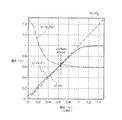
図13は、従来のボルテージフォロワ回路である図12の入力電圧と出力電圧の関係を示している。図13の横軸は入力端子INの電圧V(IN)を示し、縦軸は出力端子OUTの電圧V(OUT)、接点OUTbの電圧V(OUTb)および入力電圧INの電圧V(IN)を示している。この図では、接点OUTbと出力端子OUTの電位が等しくなるのは入力電圧が1.04Vの時である。仮に目標電圧を0.65Vとすると、40mV程度のオフセットが発生しており、この誤差は6.1%と無視できない大きさである。 FIG. 13 shows the relationship between the input voltage and output voltage of FIG. 12, which is a conventional voltage follower circuit. The horizontal axis of FIG. 13 shows the voltage V (IN) of the input terminal IN, and the vertical axis shows the voltage V (OUT) of the output terminal OUT, the voltage V (OUTb) of the contact OUTb, and the voltage V (IN) of the input voltage IN. Show. In this figure, the contact OUTb and the output terminal OUT have the same potential when the input voltage is 1.04V. If the target voltage is 0.65 V, an offset of about 40 mV is generated, and this error is 6.1% and cannot be ignored.
一方、図3は、本発明の第1の実施の形態を用いた場合の図2の回路の入力電圧と出力電圧の関係を示している。この図では、R1=R2としてV(OUT)とV(OUTb)の交点を目標電圧のV0=0.65Vに近くなるように設定しており、目標電圧V0=0.65V付近でオフセットがゼロである事が分かる。 On the other hand, FIG. 3 shows the relationship between the input voltage and the output voltage of the circuit of FIG. 2 when the first embodiment of the present invention is used. In this figure, the intersection of V (OUT) and V (OUTb) is set to be close to the target voltage V0 = 0.65V with R1 = R2, and the offset is zero near the target voltage V0 = 0.65V. I understand that.
次に本発明の他の実施の形態について図面を用いて詳細に説明する。 Next, another embodiment of the present invention will be described in detail with reference to the drawings.
[第2の実施の形態]
図4は本発明の第2の実施の形態の差動増幅回路を用いて構成したボルテージフォロワ回路の例を示している。第1の実施の形態の場合には、予め目標電圧が与えられている場合に適しているが、図4の場合は、比較的広い範囲で任意の電圧に対してオフセットを抑制する事が可能である。なお、図4において、図2と同一の構成には同一の参照符号を付けている。
[Second Embodiment]
FIG. 4 shows an example of a voltage follower circuit configured using the differential amplifier circuit according to the second embodiment of the present invention. In the case of the first embodiment, it is suitable when the target voltage is given in advance, but in the case of FIG. 4, it is possible to suppress the offset with respect to an arbitrary voltage in a relatively wide range. It is. In FIG. 4, the same components as those in FIG. 2 are denoted by the same reference numerals.
図4の回路は、図2の第1の実施の形態の抵抗R1をPチャネルMOSトランジスタM5で置き換え、そのゲート電圧を出力電圧V(OUT)に応じて制御する事で(より詳細には出力電圧V(OUT)と接点OUTbの電圧V(OUTb)の電位差を無くすように制御する事で)、任意の目標電圧に対応できるようにしたものである。トランジスタM5のゲート電圧制御手段として差動増幅回路A1を設け、その正入力端子を出力端子OUTに、負入力端子を接点OUTbに接続している。この回路の場合、トランジスタM5は可変抵抗素子として動作しており、接点OUTbの電位を出力端子OUTと等しくする動作の原理は、第1の実施の形態と同じである。 In the circuit of FIG. 4, the resistor R1 in the first embodiment of FIG. 2 is replaced with a P-channel MOS transistor M5, and its gate voltage is controlled according to the output voltage V (OUT) (more specifically, output). By controlling so as to eliminate the potential difference between the voltage V (OUT) and the voltage V (OUTb) of the contact OUTb), it can cope with an arbitrary target voltage. A differential amplifier circuit A1 is provided as a gate voltage control means of the transistor M5, and its positive input terminal is connected to the output terminal OUT and its negative input terminal is connected to the contact OUTb. In this circuit, the transistor M5 operates as a variable resistance element, and the principle of operation for making the potential of the contact OUTb equal to the output terminal OUT is the same as that in the first embodiment.
図5は、図4のゲート電圧制御手段の具体的な回路例である。トランジスタM6〜M10で図4の差動増幅回路A1を構成している。図5において、トランジスタM9およびM10は互いにゲートが接続されたPチャネルMOSトランジスタ、トランジスタM7およびM8はトランジスタM9およびM10と各ドレインが接続されるとともに、それぞれのゲートが接点OUTbおよび出力端子OUTに接続されたNチャネルMOSトランジスタ、そしてトランジスタM6はドレインがトランジスタM7およびM8のソースに、ゲートがVbias端子に接続されたNチャネルMOSトランジスタである。また、トランジスタM9およびM10のソースが電源VDDに、トランジスタM9のゲートがトランジスタM9のドレインに、トランジスタM8のドレインがトランジスタM5のゲートに、そしてトランジスタM6のソースが接地VSSに、それぞれ接続されている。 FIG. 5 is a specific circuit example of the gate voltage control means of FIG. The differential amplifier circuit A1 of FIG. 4 is configured by the transistors M6 to M10. In FIG. 5, transistors M9 and M10 are P-channel MOS transistors whose gates are connected to each other. Transistors M7 and M8 are connected to the drains of transistors M9 and M10 and their gates are connected to contact OUTb and output terminal OUT. The N-channel MOS transistor, and the transistor M6, are N-channel MOS transistors whose drains are connected to the sources of the transistors M7 and M8 and whose gates are connected to the Vbias terminal. The sources of the transistors M9 and M10 are connected to the power supply VDD, the gate of the transistor M9 is connected to the drain of the transistor M9, the drain of the transistor M8 is connected to the gate of the transistor M5, and the source of the transistor M6 is connected to the ground VSS. .
図6は、図5の回路の入力電圧と出力電圧の関係を示している。0.4V〜1.1V程度の比較的広い範囲でオフセット電圧が抑制されている事が分かる。 FIG. 6 shows the relationship between the input voltage and the output voltage of the circuit of FIG. It can be seen that the offset voltage is suppressed in a relatively wide range of about 0.4V to 1.1V.
[第3の実施の形態]
図7は、本発明の第3の実施の形態の差動増幅回路を用いて構成したボルテージフォロワ回路の例を示している。図2の第1の実施の形態の抵抗R2をNチャネルMOSトランジスタM11で置き換え、そのゲート電圧を出力電圧V(OUT)に応じて制御する事で(より詳細には出力電圧V(OUT)と接点OUTbの電圧V(OUTb)の電位差を無くすように制御する事で)、任意の目標電圧に対応できるようにしたものである。トランジスタM11のゲート電圧制御手段として差動増幅回路A1を設け、その正入力端子を出力端子OUTに、負入力端子を接点OUTbに接続している。この回路の場合、トランジスタM11は可変抵抗素子というよりは、ソースフォロワ回路として動作する事になる。即ち、トランジスタM11のゲート電位は、トランジスタM11のゲート・ソース間電圧をVGS11とすると、V(OUT)+VGS11であり、このVGS11は抵抗R1の電圧降下R1・I3がトランジスタM3のゲート・ソース間電圧VGS3になるように決まる。このVGS3とVGS11はV(OUT)にはあまり依存しないので、ほぼ一定と見做す事ができるので、トランジスタM11はソースフォロワ回路として動作する事が分かる。トランジスタM11と差動増幅回路A1によって、接点OUTbと出力端子OUTは等しい電圧に制御されるので、式1に従ってオフセット電圧がゼロになる。
[Third Embodiment]
FIG. 7 shows an example of a voltage follower circuit configured using the differential amplifier circuit according to the third embodiment of the present invention. The resistor R2 of the first embodiment in FIG. 2 is replaced with an N-channel MOS transistor M11, and its gate voltage is controlled according to the output voltage V (OUT) (more specifically, the output voltage V (OUT) and By controlling to eliminate the potential difference of the voltage V (OUTb) of the contact OUTb), it is possible to cope with an arbitrary target voltage. A differential amplifier circuit A1 is provided as a gate voltage control means of the transistor M11, and its positive input terminal is connected to the output terminal OUT and its negative input terminal is connected to the contact OUTb. In this circuit, the transistor M11 operates as a source follower circuit rather than a variable resistance element. That is, the gate potential of the transistor M11 is V (OUT) + VGS11 when the voltage between the gate and the source of the transistor M11 is VGS11. This VGS11 is the voltage drop R1 and I3 of the resistor R1 and the voltage between the gate and the source of the transistor M3. Decided to become VGS3. Since VGS3 and VGS11 do not depend much on V (OUT), they can be considered to be almost constant, and it can be seen that the transistor M11 operates as a source follower circuit. Since the contact OUTb and the output terminal OUT are controlled to the same voltage by the transistor M11 and the differential amplifier circuit A1, the offset voltage becomes zero according to
[第4の実施の形態]
図8は、本発明の第4の実施の形態の差動増幅回路を用いて構成したボルテージフォロワ回路の例を示している。図7のゲート電圧制御手段である差動増幅回路A1を抵抗R3とNチャネルMOSトランジスタM12で置き換えた構成になっている。すなわち、差動増幅回路A1を無くし、一端が電源VDDに接続され他端がトランジスタM12のドレインに接続された抵抗R3と、ゲートがドレインおよびトランジスタM11のゲートに接続されソースが出力端子OUTに接続されたトランジスタM12を設けている。
[Fourth Embodiment]
FIG. 8 shows an example of a voltage follower circuit configured using the differential amplifier circuit according to the fourth embodiment of the present invention. The differential amplifier circuit A1, which is the gate voltage control means of FIG. 7, is replaced with a resistor R3 and an N-channel MOS transistor M12. That is, the differential amplifier circuit A1 is eliminated, the resistor R3 having one end connected to the power supply VDD and the other end connected to the drain of the transistor M12, the gate connected to the drain and the gate of the transistor M11, and the source connected to the output terminal OUT. The transistor M12 is provided.
説明を簡単にする為に、仮定として、R1=R3であり、トランジスタM11とM12のトランジスタサイズは等しいとする。また、抵抗R1とR3に流れる電流I3とI4は、トランジスタM3とM4に流れる電流I1とI2に比較して無視できる程度に小さいものとする。この時、トランジスタM11とM12のゲート電位V(Ngate)は、V(Ngate)=V(OUT)+VGS12である。従って、接点OUTbの電位は、V(OUTb)=V(Ngate)−VGS11=V(OUT)+VGS12−VGS11となり、上記の仮定よりVGS11=VGS12であるから、V(OUTb)=V(OUT)である事が分かる。これにより、式1に従ってオフセット電圧がゼロになる。この例では、差動増幅回路A1が不要であり、回路の面積増加も抑えられる。
In order to simplify the explanation, it is assumed that R1 = R3 and the transistor sizes of the transistors M11 and M12 are equal. Further, the currents I3 and I4 flowing through the resistors R1 and R3 are assumed to be negligibly small compared to the currents I1 and I2 flowing through the transistors M3 and M4. At this time, the gate potential V (Ngate) of the transistors M11 and M12 is V (Ngate) = V (OUT) + VGS12. Therefore, the potential of the contact OUTb is V (OUTb) = V (Ngate) −VGS11 = V (OUT) + VGS12−VGS11, and since VGS11 = VGS12 from the above assumption, V (OUTb) = V (OUT) I understand that there is. As a result, the offset voltage becomes zero according to
図9は、図8の回路の入力電圧と出力電圧の関係を示している。0.4V〜1.1V程度の比較的広い範囲でオフセット電圧が抑制されている事が分かる。 FIG. 9 shows the relationship between the input voltage and the output voltage of the circuit of FIG. It can be seen that the offset voltage is suppressed in a relatively wide range of about 0.4V to 1.1V.
[第5の実施の形態]
図10は、本発明の第5の実施の形態の差動増幅回路を用いて構成したボルテージフォロワ回路の例を示している。図8の抵抗R1とR3をPチャネルMOSトランジスタM13、M14に置き換えたものである。すなわち、抵抗R1とR3を無くし、ソースを電源VDDにドレインをトランジスタM11のドレインに接続したトランジスタM13と、ソースを電源VDDにドレインをトランジスタM12のドレインに接続したトランジスタM14を設けている。抵抗よりもMOSトランジスタで抵抗手段を代替したほうが面積の節約ができる場合に有効である。
[Fifth Embodiment]
FIG. 10 shows an example of a voltage follower circuit configured using the differential amplifier circuit according to the fifth embodiment of the present invention. The resistors R1 and R3 in FIG. 8 are replaced with P-channel MOS transistors M13 and M14. That is, resistors R1 and R3 are eliminated, and a transistor M13 having a source connected to the power supply VDD and a drain connected to the drain of the transistor M11, and a transistor M14 having a source connected to the power supply VDD and a drain connected to the drain of the transistor M12 are provided. Replacing the resistance means with a MOS transistor rather than a resistor is effective when the area can be saved.
[効果の説明]
これまでの説明で既に明らかであるように、上記の各実施の形態は、図1の出力端子OUTと接点OUTbの電位を等しくする事により、差動増幅回路の入力オフセット電圧を抑制する事が可能である。
[Description of effects]
As is apparent from the above description, each of the above embodiments can suppress the input offset voltage of the differential amplifier circuit by equalizing the potentials of the output terminal OUT and the contact OUTb in FIG. Is possible.
また、動作電源電圧マージンを損なう事が無いという利点もある。この点について多少の説明を加えると、従来の差動増幅回路の図12の例と、本発明の図2を比較した場合、回路の各トランジスタの動作点は、接点OUTbの電位の違いしか生じていない。一方、図2のトランジスタM0−トランジスタM2−トランジスタM4のパスで必要な最低電圧とトランジスタM0−トランジスタM1−トランジスタM3のパスで必要な最低電圧は等しいので、この回路の最低動作電圧はトランジスタM0−トランジスタM2−トランジスタM4のパスのみで決まると考えて差し支えない。図2の構成におけるこのパスの動作点は図12の従来の差動増幅回路と等しいので、少なくとも従来の差動増幅回路の動作電源電圧マージンを損なう事は無いのである。 There is also an advantage that the operating power supply voltage margin is not impaired. To add a little explanation about this point, when the example of the conventional differential amplifier circuit of FIG. 12 is compared with FIG. 2 of the present invention, the operating point of each transistor of the circuit is only the difference in the potential of the contact OUTb. Not. On the other hand, the minimum voltage required for the path of transistor M0-transistor M2-transistor M4 and the minimum voltage required for the path of transistor M0-transistor M1-transistor M3 in FIG. It can be considered that it is determined only by the path of transistor M2-transistor M4. Since the operating point of this path in the configuration of FIG. 2 is the same as that of the conventional differential amplifier circuit of FIG. 12, at least the operating power supply voltage margin of the conventional differential amplifier circuit is not impaired.
上記の実施の形態の説明では、入力オフセットの説明の為に、便宜上本発明をボルテージフォロワ回路に適用した場合について説明して来たが、決してボルテージフォロワ回路に限定されるものではなく、演算増幅器として使用される差動増幅回路として一般的に適用可能である。 In the above description of the embodiment, the case where the present invention is applied to a voltage follower circuit has been described for the sake of convenience in order to explain the input offset. However, the present invention is not limited to a voltage follower circuit. It is generally applicable as a differential amplifier circuit used as
なお、上記の本発明の実施の形態は、上記のものに限定されず、例えば位相補償用などのために容量を付加することや、抵抗素子を直列あるいは並列に複数に分けて構成することや、トランジスタを並列に分けて構成することなどの変更が適宜可能である。 The embodiments of the present invention described above are not limited to the above-described ones. For example, a capacitor is added for phase compensation or the like, and the resistance elements are divided into a plurality of series or parallel parts. It is possible to appropriately change the configuration such as dividing the transistors in parallel.
1 差動トランジスタ対
2 定電流源回路
3 カレントミラー負荷回路
4 バイアス発生回路
M3、M4、M5、M9、M10、M13、M14 PチャネルMOSトランジスタ
M0、M1、M2、M6、M7、M8、M11、M12 NチャネルMOSトランジスタ
R1、R2、R3 抵抗
A1、DA1 差動増幅回路
1 differential transistor pair 2 constant
M3, M4, M5, M9, M10, M13, M14 P-channel MOS transistors
M0, M1, M2, M6, M7, M8, M11, M12 N-channel MOS transistors
R1, R2, R3 resistance
A1, DA1 differential amplifier
Claims (6)
差動トランジスタ対のソースと接地との間に接続された定電流源回路と、
1対のPチャネルMOSトランジスタからなり、各トランジスタのゲートが互いに接続され、各トランジスタのソースが電源に接続され、各トランジスタのドレインが差動トランジスタ対の各トランジスタの各ドレインにそれぞれ接続されたカレントミラー負荷回路と、
カレントミラー負荷回路の各トランジスタの各ドレインの一方の電位と他方の電位を等しくするように、各トランジスタのゲートバイアスおよびドレインバイアスを発生するバイアス発生回路とを備え、
前記バイアス発生回路が、
前記カレントミラー負荷回路の各トランジスタのゲートと電源の間に接続された第1の抵抗と、
前記カレントミラー負荷回路の一方のトランジスタのドレインとゲートの間に接続された第2の抵抗素子と
からなることを特徴とする差動増幅回路。 A differential transistor pair comprising a pair of N-channel MOS transistors, a differential input signal terminal connected to the gate of each transistor, and the sources of the transistors connected to each other;
A constant current source circuit connected between the source of the differential transistor pair and ground;
A current comprising a pair of P-channel MOS transistors, the gates of the transistors being connected to each other, the sources of the transistors being connected to a power source, and the drains of the transistors being connected to the drains of the transistors of the differential transistor pair, respectively. A mirror load circuit;
A bias generation circuit for generating a gate bias and a drain bias of each transistor so that one potential of each drain of each transistor of the current mirror load circuit is equal to the other potential;
The bias generation circuit includes:
A first resistor connected between the gate of each transistor of the current mirror load circuit and a power source;
One of the drain and the gate connected to the second resistive element and the differential amplifier circuit you characterized in that it consists during the transistor of the current mirror load circuit.
差動トランジスタ対のソースと接地との間に接続された定電流源回路と、
1対のPチャネルMOSトランジスタからなり、各トランジスタのゲートが互いに接続され、各トランジスタのソースが電源に接続され、各トランジスタのドレインが差動トランジスタ対の各トランジスタの各ドレインにそれぞれ接続されたカレントミラー負荷回路と、
カレントミラー負荷回路の各トランジスタの各ドレインの一方の電位と他方の電位を等しくするように、各トランジスタのゲートバイアスおよびドレインバイアスを発生するバイアス発生回路とを備え、
前記バイアス発生回路が、
前記カレントミラー負荷回路の各トランジスタのゲートと電源の間に接続されたPチャネルMOSトランジスタと、
前記カレントミラー負荷回路の一方のトランジスタのドレインとゲートの間に接続された抵抗素子と、
そのPチャネルMOSトランジスタのゲートに出力が接続されたバイアス制御用の差動増幅回路であって、その負入力端子が前記カレントミラー負荷の一方のトランジスタのドレインに接続され、正入力端子が他方のトランジスタのドレインに接続されたものと
からなることを特徴とする差動増幅回路。 A differential transistor pair comprising a pair of N-channel MOS transistors, a differential input signal terminal connected to the gate of each transistor, and the sources of the transistors connected to each other;
A constant current source circuit connected between the source of the differential transistor pair and ground;
A current comprising a pair of P-channel MOS transistors, the gates of the transistors being connected to each other, the sources of the transistors being connected to a power source, and the drains of the transistors being connected to the drains of the transistors of the differential transistor pair, respectively. A mirror load circuit;
A bias generation circuit for generating a gate bias and a drain bias of each transistor so that one potential of each drain of each transistor of the current mirror load circuit is equal to the other potential;
The bias generation circuit includes:
A P-channel MOS transistor connected between the gate of each transistor of the current mirror load circuit and a power supply;
A resistance element connected between the drain and gate of one transistor of the current mirror load circuit;
A differential amplifier circuit for bias control in which an output is connected to the gate of the P-channel MOS transistor, the negative input terminal is connected to the drain of one transistor of the current mirror load, and the positive input terminal is the other differential amplifier circuit characterized in that it consists to have been connected to the drain of the transistor.
差動トランジスタ対のソースと接地との間に接続された定電流源回路と、
1対のPチャネルMOSトランジスタからなり、各トランジスタのゲートが互いに接続され、各トランジスタのソースが電源に接続され、各トランジスタのドレインが差動トランジスタ対の各トランジスタの各ドレインにそれぞれ接続されたカレントミラー負荷回路と、
カレントミラー負荷回路の各トランジスタの各ドレインの一方の電位と他方の電位を等しくするように、各トランジスタのゲートバイアスおよびドレインバイアスを発生するバイアス発生回路とを備え、
前記バイアス発生回路が、
前記カレントミラー負荷回路の各トランジスタのゲートと電源の間に接続された抵抗素子と、
前記カレントミラー負荷回路の一方のトランジスタのドレインとゲートの間に接続されたNチャネルMOSトランジスタと、
そのNチャネルMOSトランジスタのゲートに出力が接続されたバイアス制御用の差動増幅回路であって、その負入力端子が前記カレントミラー負荷の一方のトランジスタのドレインに接続され、正入力端子が他方のトランジスタのドレインに接続されたものと
からなることを特徴とする差動増幅回路。 A differential transistor pair comprising a pair of N-channel MOS transistors, a differential input signal terminal connected to the gate of each transistor, and the sources of the transistors connected to each other;
A constant current source circuit connected between the source of the differential transistor pair and ground;
A current comprising a pair of P-channel MOS transistors, the gates of the transistors being connected to each other, the sources of the transistors being connected to a power source, and the drains of the transistors being connected to the drains of the transistors of the differential transistor pair, respectively. A mirror load circuit;
A bias generation circuit for generating a gate bias and a drain bias of each transistor so that one potential of each drain of each transistor of the current mirror load circuit is equal to the other potential;
The bias generation circuit includes:
A resistive element connected between the gate of each transistor of the current mirror load circuit and a power supply;
An N-channel MOS transistor connected between the drain and gate of one transistor of the current mirror load circuit;
A bias control differential amplifier circuit having an output connected to the gate of the N-channel MOS transistor, the negative input terminal connected to the drain of one transistor of the current mirror load, and the positive input terminal connected to the other differential amplifier circuit characterized in that it consists to have been connected to the drain of the transistor.
差動トランジスタ対のソースと接地との間に接続された定電流源回路と、
1対のPチャネルMOSトランジスタからなり、各トランジスタのゲートが互いに接続され、各トランジスタのソースが電源に接続され、各トランジスタのドレインが差動トランジスタ対の各トランジスタの各ドレインにそれぞれ接続されたカレントミラー負荷回路と、
カレントミラー負荷回路の各トランジスタの各ドレインの一方の電位と他方の電位を等しくするように、各トランジスタのゲートバイアスおよびドレインバイアスを発生するバイアス発生回路とを備え、
前記バイアス発生回路が、
前記カレントミラー負荷回路の各トランジスタのゲートと電源の間に接続された第1の抵抗素子と、
前記カレントミラー負荷回路の一方のトランジスタのドレインとゲートの間に接続された第1のNチャネルMOSトランジスタと、
前記カレントミラー負荷回路の他方のトランジスタのドレインにソースを接続され、ゲートとドレインが第1のNチャネルMOSトランジスタのゲートに接続された第2のNチャネルMOSトランジスタと
電源と第2のNチャネルMOSのゲートの間に接続された第2の抵抗素子と
からなることを特徴とする差動増幅回路。 A differential transistor pair comprising a pair of N-channel MOS transistors, a differential input signal terminal connected to the gate of each transistor, and the sources of the transistors connected to each other;
A constant current source circuit connected between the source of the differential transistor pair and ground;
A current comprising a pair of P-channel MOS transistors, the gates of the transistors being connected to each other, the sources of the transistors being connected to a power source, and the drains of the transistors being connected to the drains of the transistors of the differential transistor pair, respectively. A mirror load circuit;
A bias generation circuit for generating a gate bias and a drain bias of each transistor so that one potential of each drain of each transistor of the current mirror load circuit is equal to the other potential;
The bias generation circuit includes:
A first resistance element connected between the gate of each transistor of the current mirror load circuit and a power supply;
A first N-channel MOS transistor connected between the drain and gate of one transistor of the current mirror load circuit;
A second N-channel MOS transistor having a source connected to the drain of the other transistor of the current mirror load circuit, a gate and a drain connected to the gate of the first N-channel MOS transistor, a power supply, and a second N-channel MOS the second resistive element and the differential amplifier circuit characterized in that it consists of which is connected between the gate of the.
ことを特徴とする請求項4に記載の差動増幅回路。 5. The differential amplifier circuit according to claim 4 , wherein each of the first resistance element and the second resistance element is replaced with a MOS transistor.
ことを特徴とする請求項1〜5のいずれか1項に記載の差動増幅回路。 One and of the differential input signal terminals, any one of the preceding claims, characterized in that it forms a voltage follower circuit by connecting the drain of one transistor of said current mirror load circuit The differential amplifier circuit according to 1.
Priority Applications (2)
| Application Number | Priority Date | Filing Date | Title |
|---|---|---|---|
| JP2007264532A JP5543059B2 (en) | 2007-10-10 | 2007-10-10 | Differential amplifier circuit |
| US12/285,598 US7859339B2 (en) | 2007-10-10 | 2008-10-09 | Differential amplification circuit |
Applications Claiming Priority (1)
| Application Number | Priority Date | Filing Date | Title |
|---|---|---|---|
| JP2007264532A JP5543059B2 (en) | 2007-10-10 | 2007-10-10 | Differential amplifier circuit |
Publications (2)
| Publication Number | Publication Date |
|---|---|
| JP2009094878A JP2009094878A (en) | 2009-04-30 |
| JP5543059B2 true JP5543059B2 (en) | 2014-07-09 |
Family
ID=40533600
Family Applications (1)
| Application Number | Title | Priority Date | Filing Date |
|---|---|---|---|
| JP2007264532A Expired - Fee Related JP5543059B2 (en) | 2007-10-10 | 2007-10-10 | Differential amplifier circuit |
Country Status (2)
| Country | Link |
|---|---|
| US (1) | US7859339B2 (en) |
| JP (1) | JP5543059B2 (en) |
Families Citing this family (5)
| Publication number | Priority date | Publication date | Assignee | Title |
|---|---|---|---|---|
| JP2011155488A (en) * | 2010-01-27 | 2011-08-11 | Ricoh Co Ltd | Differential input stage circuit, operational amplifier including the same, and voltage regulator circuit |
| US8928408B2 (en) * | 2013-01-24 | 2015-01-06 | Aeroflex Colorado Springs Inc. | High-gain low-noise preamplifier and associated amplification and common-mode control method |
| JP6082297B2 (en) * | 2013-03-27 | 2017-02-15 | 新日本無線株式会社 | Current source circuit |
| DE102014109118B4 (en) * | 2014-06-30 | 2016-01-14 | Intel IP Corporation | Circuit, integrated circuit, receiver, transceiver and method for amplifying an input signal |
| WO2016090248A1 (en) * | 2014-12-05 | 2016-06-09 | Analog Devices, Inc. | High gain load circuit for a differential pair using depletion mode transistors |
Family Cites Families (15)
| Publication number | Priority date | Publication date | Assignee | Title |
|---|---|---|---|---|
| US4334196A (en) * | 1980-03-18 | 1982-06-08 | Rca Corporation | Amplifier using lateral and vertical transistors |
| JPS6253512A (en) * | 1985-09-03 | 1987-03-09 | Anritsu Corp | Pulse output device |
| JPS62104305A (en) | 1985-10-31 | 1987-05-14 | Toshiba Corp | Current mirror circuit |
| JPH0697490B2 (en) | 1987-09-28 | 1994-11-30 | シャープ株式会社 | Double azimuth head |
| JPS6486606A (en) * | 1987-09-28 | 1989-03-31 | Nec Corp | Operational amplifier circuit |
| US4972158A (en) * | 1989-10-31 | 1990-11-20 | International Business Machines Corporation | Transistor amplifier with variable bias circuits |
| JPH03169107A (en) | 1989-11-28 | 1991-07-22 | Nec Corp | Current mirror circuit |
| JPH0514075A (en) | 1991-07-05 | 1993-01-22 | Matsushita Electric Ind Co Ltd | Differential amplifier circuit |
| JPH11510672A (en) * | 1996-05-22 | 1999-09-14 | フィリップス エレクトロニクス ネムローゼ フェンノートシャップ | Amplifiers using active bootstrap gain enhancement technology. |
| JPH11284448A (en) * | 1998-03-31 | 1999-10-15 | Nec Corp | Differential amplifier |
| JP4029958B2 (en) * | 2001-04-16 | 2008-01-09 | 日本電信電話株式会社 | Semiconductor circuit |
| JP4251826B2 (en) * | 2002-06-26 | 2009-04-08 | 株式会社リコー | Constant voltage circuit |
| US6967532B2 (en) * | 2003-12-30 | 2005-11-22 | Intel Corporation | Offset-compensated self-biased differential amplifier |
| JP4703133B2 (en) | 2004-05-25 | 2011-06-15 | ルネサスエレクトロニクス株式会社 | Internal voltage generation circuit and semiconductor integrated circuit device |
| CN101375499A (en) * | 2006-01-31 | 2009-02-25 | Nxp股份有限公司 | Current mirror circuit |
-
2007
- 2007-10-10 JP JP2007264532A patent/JP5543059B2/en not_active Expired - Fee Related
-
2008
- 2008-10-09 US US12/285,598 patent/US7859339B2/en not_active Expired - Fee Related
Also Published As
| Publication number | Publication date |
|---|---|
| US20090096523A1 (en) | 2009-04-16 |
| JP2009094878A (en) | 2009-04-30 |
| US7859339B2 (en) | 2010-12-28 |
Similar Documents
| Publication | Publication Date | Title |
|---|---|---|
| JP4834347B2 (en) | Constant current circuit | |
| CN101615049B (en) | Reference buffer circuit | |
| JP4800781B2 (en) | Voltage level shift circuit and semiconductor integrated circuit | |
| JP5657853B2 (en) | Constant current source circuit | |
| JP4676885B2 (en) | Bias circuit | |
| JP5690469B2 (en) | Differential amplifier, reference voltage generation circuit, differential amplification method, and reference voltage generation method | |
| JP5334180B2 (en) | Voltage divider circuit | |
| JP5543059B2 (en) | Differential amplifier circuit | |
| JP5092687B2 (en) | Amplifier and Gm compensation bias circuit | |
| JP2005244276A (en) | Differential amplification circuit | |
| JP4058334B2 (en) | Hysteresis comparator circuit | |
| JP4829650B2 (en) | Differential amplifier circuit | |
| TW201838327A (en) | Transconductance amplifier | |
| JP4555131B2 (en) | Constant voltage power circuit | |
| JP2012216171A (en) | Reference voltage circuit | |
| JP6949463B2 (en) | Single differential conversion circuit | |
| JP6705233B2 (en) | Offset correction circuit and transconductance proportional current generation circuit | |
| JP2007180796A (en) | Differential amplifier circuit | |
| JP2000252768A (en) | Operational amplifier | |
| JP2015046193A (en) | Constant current source circuit | |
| JP4819583B2 (en) | OTA circuit | |
| JP7025498B2 (en) | Memory control device and memory control method | |
| KR100338340B1 (en) | Operational amplifier | |
| JP2005080090A (en) | Output voltage control circuit of differential amplifier circuit and voltage detector | |
| JP5203809B2 (en) | Current mirror circuit |
Legal Events
| Date | Code | Title | Description |
|---|---|---|---|
| A621 | Written request for application examination |
Free format text: JAPANESE INTERMEDIATE CODE: A621 Effective date: 20100913 |
|
| A977 | Report on retrieval |
Free format text: JAPANESE INTERMEDIATE CODE: A971007 Effective date: 20111027 |
|
| A711 | Notification of change in applicant |
Free format text: JAPANESE INTERMEDIATE CODE: A711 Effective date: 20130731 |
|
| A521 | Written amendment |
Free format text: JAPANESE INTERMEDIATE CODE: A821 Effective date: 20130801 |
|
| A521 | Written amendment |
Free format text: JAPANESE INTERMEDIATE CODE: A523 Effective date: 20130905 |
|
| A131 | Notification of reasons for refusal |
Free format text: JAPANESE INTERMEDIATE CODE: A131 Effective date: 20131008 |
|
| RD03 | Notification of appointment of power of attorney |
Free format text: JAPANESE INTERMEDIATE CODE: A7423 Effective date: 20131030 |
|
| RD04 | Notification of resignation of power of attorney |
Free format text: JAPANESE INTERMEDIATE CODE: A7424 Effective date: 20131213 |
|
| A601 | Written request for extension of time |
Free format text: JAPANESE INTERMEDIATE CODE: A601 Effective date: 20131226 |
|
| A602 | Written permission of extension of time |
Free format text: JAPANESE INTERMEDIATE CODE: A602 Effective date: 20140107 |
|
| A521 | Written amendment |
Free format text: JAPANESE INTERMEDIATE CODE: A523 Effective date: 20140403 |
|
| TRDD | Decision of grant or rejection written | ||
| A01 | Written decision to grant a patent or to grant a registration (utility model) |
Free format text: JAPANESE INTERMEDIATE CODE: A01 Effective date: 20140422 |
|
| A61 | First payment of annual fees (during grant procedure) |
Free format text: JAPANESE INTERMEDIATE CODE: A61 Effective date: 20140508 |
|
| R150 | Certificate of patent or registration of utility model |
Ref document number: 5543059 Country of ref document: JP Free format text: JAPANESE INTERMEDIATE CODE: R150 |
|
| LAPS | Cancellation because of no payment of annual fees |