JP5520633B2 - Display device with touch panel - Google Patents
Display device with touch panel Download PDFInfo
- Publication number
- JP5520633B2 JP5520633B2 JP2010040086A JP2010040086A JP5520633B2 JP 5520633 B2 JP5520633 B2 JP 5520633B2 JP 2010040086 A JP2010040086 A JP 2010040086A JP 2010040086 A JP2010040086 A JP 2010040086A JP 5520633 B2 JP5520633 B2 JP 5520633B2
- Authority
- JP
- Japan
- Prior art keywords
- electrode
- touch panel
- display device
- display
- panel
- Prior art date
- Legal status (The legal status is an assumption and is not a legal conclusion. Google has not performed a legal analysis and makes no representation as to the accuracy of the status listed.)
- Active
Links
- 125000006850 spacer group Chemical group 0.000 claims description 42
- 238000001514 detection method Methods 0.000 claims description 36
- 239000011324 bead Substances 0.000 claims description 10
- 238000009434 installation Methods 0.000 claims 1
- 239000010408 film Substances 0.000 description 71
- 239000000758 substrate Substances 0.000 description 34
- 239000000463 material Substances 0.000 description 27
- 239000000853 adhesive Substances 0.000 description 24
- 230000001070 adhesive effect Effects 0.000 description 24
- 229920005989 resin Polymers 0.000 description 17
- 239000011347 resin Substances 0.000 description 17
- 238000000034 method Methods 0.000 description 15
- 238000010586 diagram Methods 0.000 description 11
- NIXOWILDQLNWCW-UHFFFAOYSA-M Acrylate Chemical compound [O-]C(=O)C=C NIXOWILDQLNWCW-UHFFFAOYSA-M 0.000 description 10
- 238000003825 pressing Methods 0.000 description 10
- 239000011521 glass Substances 0.000 description 9
- 238000002834 transmittance Methods 0.000 description 8
- 238000010168 coupling process Methods 0.000 description 7
- 239000010419 fine particle Substances 0.000 description 7
- 239000002313 adhesive film Substances 0.000 description 6
- -1 polyethylene terephthalate Polymers 0.000 description 6
- 229920000139 polyethylene terephthalate Polymers 0.000 description 6
- 239000005020 polyethylene terephthalate Substances 0.000 description 6
- 229920002050 silicone resin Polymers 0.000 description 6
- SKRWFPLZQAAQSU-UHFFFAOYSA-N stibanylidynetin;hydrate Chemical compound O.[Sn].[Sb] SKRWFPLZQAAQSU-UHFFFAOYSA-N 0.000 description 6
- 238000004364 calculation method Methods 0.000 description 5
- 229920001971 elastomer Polymers 0.000 description 5
- 238000005530 etching Methods 0.000 description 5
- 238000005498 polishing Methods 0.000 description 5
- 238000006116 polymerization reaction Methods 0.000 description 5
- 239000005060 rubber Substances 0.000 description 5
- 239000003822 epoxy resin Substances 0.000 description 4
- 238000004519 manufacturing process Methods 0.000 description 4
- 239000002245 particle Substances 0.000 description 4
- 229920002492 poly(sulfone) Polymers 0.000 description 4
- 229920001230 polyarylate Polymers 0.000 description 4
- 229920000647 polyepoxide Polymers 0.000 description 4
- 229920001225 polyester resin Polymers 0.000 description 4
- 239000004645 polyester resin Substances 0.000 description 4
- 239000010409 thin film Substances 0.000 description 4
- OEPOKWHJYJXUGD-UHFFFAOYSA-N 2-(3-phenylmethoxyphenyl)-1,3-thiazole-4-carbaldehyde Chemical compound O=CC1=CSC(C=2C=C(OCC=3C=CC=CC=3)C=CC=2)=N1 OEPOKWHJYJXUGD-UHFFFAOYSA-N 0.000 description 3
- JOYRKODLDBILNP-UHFFFAOYSA-N Ethyl urethane Chemical compound CCOC(N)=O JOYRKODLDBILNP-UHFFFAOYSA-N 0.000 description 3
- 229920000459 Nitrile rubber Polymers 0.000 description 3
- 229910006404 SnO 2 Inorganic materials 0.000 description 3
- XTXRWKRVRITETP-UHFFFAOYSA-N Vinyl acetate Chemical compound CC(=O)OC=C XTXRWKRVRITETP-UHFFFAOYSA-N 0.000 description 3
- NIXOWILDQLNWCW-UHFFFAOYSA-N acrylic acid group Chemical group C(C=C)(=O)O NIXOWILDQLNWCW-UHFFFAOYSA-N 0.000 description 3
- 239000003522 acrylic cement Substances 0.000 description 3
- 239000003513 alkali Substances 0.000 description 3
- AMGQUBHHOARCQH-UHFFFAOYSA-N indium;oxotin Chemical compound [In].[Sn]=O AMGQUBHHOARCQH-UHFFFAOYSA-N 0.000 description 3
- 229920006122 polyamide resin Polymers 0.000 description 3
- 238000007650 screen-printing Methods 0.000 description 3
- 239000000243 solution Substances 0.000 description 3
- 229920003051 synthetic elastomer Polymers 0.000 description 3
- 239000005061 synthetic rubber Substances 0.000 description 3
- 230000000007 visual effect Effects 0.000 description 3
- YVTHLONGBIQYBO-UHFFFAOYSA-N zinc indium(3+) oxygen(2-) Chemical compound [O--].[Zn++].[In+3] YVTHLONGBIQYBO-UHFFFAOYSA-N 0.000 description 3
- BMYNFMYTOJXKLE-UHFFFAOYSA-N 3-azaniumyl-2-hydroxypropanoate Chemical compound NCC(O)C(O)=O BMYNFMYTOJXKLE-UHFFFAOYSA-N 0.000 description 2
- KRHYYFGTRYWZRS-UHFFFAOYSA-N Fluorane Chemical compound F KRHYYFGTRYWZRS-UHFFFAOYSA-N 0.000 description 2
- 244000043261 Hevea brasiliensis Species 0.000 description 2
- PXHVJJICTQNCMI-UHFFFAOYSA-N Nickel Chemical compound [Ni] PXHVJJICTQNCMI-UHFFFAOYSA-N 0.000 description 2
- 229920012266 Poly(ether sulfone) PES Polymers 0.000 description 2
- 238000013459 approach Methods 0.000 description 2
- 239000007864 aqueous solution Substances 0.000 description 2
- 239000002585 base Substances 0.000 description 2
- 238000005401 electroluminescence Methods 0.000 description 2
- 229920003049 isoprene rubber Polymers 0.000 description 2
- 229910052751 metal Inorganic materials 0.000 description 2
- 239000002184 metal Substances 0.000 description 2
- 239000000203 mixture Substances 0.000 description 2
- 229920003052 natural elastomer Polymers 0.000 description 2
- 229920001194 natural rubber Polymers 0.000 description 2
- 230000003287 optical effect Effects 0.000 description 2
- 229920003023 plastic Polymers 0.000 description 2
- 239000004033 plastic Substances 0.000 description 2
- 229920001084 poly(chloroprene) Polymers 0.000 description 2
- 229920000515 polycarbonate Polymers 0.000 description 2
- 239000004417 polycarbonate Substances 0.000 description 2
- 229920000642 polymer Polymers 0.000 description 2
- 238000004544 sputter deposition Methods 0.000 description 2
- 125000003903 2-propenyl group Chemical group [H]C([*])([H])C([H])=C([H])[H] 0.000 description 1
- 229920000178 Acrylic resin Polymers 0.000 description 1
- 239000004925 Acrylic resin Substances 0.000 description 1
- 229910018072 Al 2 O 3 Inorganic materials 0.000 description 1
- 229910015902 Bi 2 O 3 Inorganic materials 0.000 description 1
- 229910020203 CeO Inorganic materials 0.000 description 1
- RYGMFSIKBFXOCR-UHFFFAOYSA-N Copper Chemical compound [Cu] RYGMFSIKBFXOCR-UHFFFAOYSA-N 0.000 description 1
- 229920000181 Ethylene propylene rubber Polymers 0.000 description 1
- YCKRFDGAMUMZLT-UHFFFAOYSA-N Fluorine atom Chemical compound [F] YCKRFDGAMUMZLT-UHFFFAOYSA-N 0.000 description 1
- 229910021193 La 2 O 3 Inorganic materials 0.000 description 1
- CERQOIWHTDAKMF-UHFFFAOYSA-N Methacrylic acid Chemical compound CC(=C)C(O)=O CERQOIWHTDAKMF-UHFFFAOYSA-N 0.000 description 1
- 229920001609 Poly(3,4-ethylenedioxythiophene) Polymers 0.000 description 1
- 239000005062 Polybutadiene Substances 0.000 description 1
- 239000004820 Pressure-sensitive adhesive Substances 0.000 description 1
- 229910004298 SiO 2 Inorganic materials 0.000 description 1
- BQCADISMDOOEFD-UHFFFAOYSA-N Silver Chemical compound [Ag] BQCADISMDOOEFD-UHFFFAOYSA-N 0.000 description 1
- CDBYLPFSWZWCQE-UHFFFAOYSA-L Sodium Carbonate Chemical compound [Na+].[Na+].[O-]C([O-])=O CDBYLPFSWZWCQE-UHFFFAOYSA-L 0.000 description 1
- 229910010413 TiO 2 Inorganic materials 0.000 description 1
- 229920006311 Urethane elastomer Polymers 0.000 description 1
- 239000006061 abrasive grain Substances 0.000 description 1
- 239000000654 additive Substances 0.000 description 1
- 229920006223 adhesive resin Polymers 0.000 description 1
- HSFWRNGVRCDJHI-UHFFFAOYSA-N alpha-acetylene Natural products C#C HSFWRNGVRCDJHI-UHFFFAOYSA-N 0.000 description 1
- 229910052788 barium Inorganic materials 0.000 description 1
- DSAJWYNOEDNPEQ-UHFFFAOYSA-N barium atom Chemical compound [Ba] DSAJWYNOEDNPEQ-UHFFFAOYSA-N 0.000 description 1
- 239000005388 borosilicate glass Substances 0.000 description 1
- 238000012662 bulk polymerization Methods 0.000 description 1
- FACXGONDLDSNOE-UHFFFAOYSA-N buta-1,3-diene;styrene Chemical compound C=CC=C.C=CC1=CC=CC=C1.C=CC1=CC=CC=C1 FACXGONDLDSNOE-UHFFFAOYSA-N 0.000 description 1
- 125000000484 butyl group Chemical group [H]C([*])([H])C([H])([H])C([H])([H])C([H])([H])[H] 0.000 description 1
- 229920005549 butyl rubber Polymers 0.000 description 1
- 239000004020 conductor Substances 0.000 description 1
- 229920001577 copolymer Polymers 0.000 description 1
- 229910052802 copper Inorganic materials 0.000 description 1
- 239000010949 copper Substances 0.000 description 1
- 230000008878 coupling Effects 0.000 description 1
- 238000005859 coupling reaction Methods 0.000 description 1
- 230000007423 decrease Effects 0.000 description 1
- 230000006866 deterioration Effects 0.000 description 1
- 125000003438 dodecyl group Chemical group [H]C([H])([H])C([H])([H])C([H])([H])C([H])([H])C([H])([H])C([H])([H])C([H])([H])C([H])([H])C([H])([H])C([H])([H])C([H])([H])C([H])([H])* 0.000 description 1
- 238000010556 emulsion polymerization method Methods 0.000 description 1
- 229920005558 epichlorohydrin rubber Polymers 0.000 description 1
- 239000004744 fabric Substances 0.000 description 1
- 239000000945 filler Substances 0.000 description 1
- 239000011737 fluorine Substances 0.000 description 1
- 229910052731 fluorine Inorganic materials 0.000 description 1
- 238000010528 free radical solution polymerization reaction Methods 0.000 description 1
- PCHJSUWPFVWCPO-UHFFFAOYSA-N gold Chemical compound [Au] PCHJSUWPFVWCPO-UHFFFAOYSA-N 0.000 description 1
- 229910052737 gold Inorganic materials 0.000 description 1
- 239000010931 gold Substances 0.000 description 1
- LNEPOXFFQSENCJ-UHFFFAOYSA-N haloperidol Chemical compound C1CC(O)(C=2C=CC(Cl)=CC=2)CCN1CCCC(=O)C1=CC=C(F)C=C1 LNEPOXFFQSENCJ-UHFFFAOYSA-N 0.000 description 1
- 238000010438 heat treatment Methods 0.000 description 1
- 125000004051 hexyl group Chemical group [H]C([H])([H])C([H])([H])C([H])([H])C([H])([H])C([H])([H])C([H])([H])* 0.000 description 1
- 150000004678 hydrides Chemical class 0.000 description 1
- 125000002768 hydroxyalkyl group Chemical group 0.000 description 1
- 238000012905 input function Methods 0.000 description 1
- 238000009413 insulation Methods 0.000 description 1
- 125000000959 isobutyl group Chemical group [H]C([H])([H])C([H])(C([H])([H])[H])C([H])([H])* 0.000 description 1
- 239000004973 liquid crystal related substance Substances 0.000 description 1
- 239000011159 matrix material Substances 0.000 description 1
- 229910001512 metal fluoride Inorganic materials 0.000 description 1
- 229910044991 metal oxide Inorganic materials 0.000 description 1
- 150000004706 metal oxides Chemical class 0.000 description 1
- 229910052759 nickel Inorganic materials 0.000 description 1
- 238000000059 patterning Methods 0.000 description 1
- 229920000636 poly(norbornene) polymer Polymers 0.000 description 1
- 229920001197 polyacetylene Polymers 0.000 description 1
- 229920000058 polyacrylate Polymers 0.000 description 1
- 229920000767 polyaniline Polymers 0.000 description 1
- 229920002857 polybutadiene Polymers 0.000 description 1
- 229920000128 polypyrrole Polymers 0.000 description 1
- 239000005077 polysulfide Substances 0.000 description 1
- 229920001021 polysulfide Polymers 0.000 description 1
- 150000008117 polysulfides Polymers 0.000 description 1
- 229920003225 polyurethane elastomer Polymers 0.000 description 1
- 229920002379 silicone rubber Polymers 0.000 description 1
- 239000004945 silicone rubber Substances 0.000 description 1
- 229910052709 silver Inorganic materials 0.000 description 1
- 239000004332 silver Substances 0.000 description 1
- 125000004079 stearyl group Chemical group [H]C([*])([H])C([H])([H])C([H])([H])C([H])([H])C([H])([H])C([H])([H])C([H])([H])C([H])([H])C([H])([H])C([H])([H])C([H])([H])C([H])([H])C([H])([H])C([H])([H])C([H])([H])C([H])([H])C([H])([H])C([H])([H])[H] 0.000 description 1
- 229920003048 styrene butadiene rubber Polymers 0.000 description 1
- 229920000468 styrene butadiene styrene block copolymer Polymers 0.000 description 1
- 239000000725 suspension Substances 0.000 description 1
- 229920002803 thermoplastic polyurethane Polymers 0.000 description 1
- 229920001187 thermosetting polymer Polymers 0.000 description 1
- 239000005341 toughened glass Substances 0.000 description 1
- XLOMVQKBTHCTTD-UHFFFAOYSA-N zinc oxide Inorganic materials [Zn]=O XLOMVQKBTHCTTD-UHFFFAOYSA-N 0.000 description 1
- 239000011787 zinc oxide Substances 0.000 description 1
Images


Landscapes
- Position Input By Displaying (AREA)
Description
本発明は、タッチパネル付表示装置に関し、より詳しくは静電容量結合方式のタッチパネルを備える表示装置に関する。 The present invention relates to a display device with a touch panel, and more particularly to a display device including a capacitively coupled touch panel.
表示画面に利用者の指などで接触押圧操作(以下、「タッチ」という。)して情報を入力する画面入力機能をもつ入力装置(以下、「タッチパネル」という。)を備えた表示装置は、PDA(Personal Digital Assistance)や携帯端末などのモバイル用電子機器、各種の家電製品、無人受付機等の据置型顧客案内端末等に用いられている。このようなタッチパネルには、タッチされた部分の抵抗値変化を検出する抵抗膜方式、あるいは容量変化を検出する静電容量結合方式、タッチにより遮蔽された部分の光量変化を検出する光センサ方式などがある。 A display device provided with an input device (hereinafter referred to as “touch panel”) having a screen input function for inputting information by a contact pressing operation (hereinafter referred to as “touch”) with a user's finger or the like on the display screen, It is used for mobile electronic devices such as PDAs (Personal Digital Assistance) and portable terminals, various home appliances, stationary customer guidance terminals such as unmanned reception machines, and the like. Such touch panels include a resistive film method that detects a change in the resistance value of a touched portion, a capacitive coupling method that detects a change in capacitance, an optical sensor method that detects a change in the amount of light in a portion shielded by touching, etc. There is.
静電容量結合方式は、抵抗膜方式や光センサ方式では透過率が80%程度と低いのに対し、透過率が約90%と高く表示画質を低下させない利点がある。また、抵抗膜方式では抵抗膜の機械的接触によりタッチ位置を検知するため、抵抗膜が劣化または破損(クラック)するおそれがあるのに対し、静電容量結合方式では検出用電極が他の電極などと接触するような機械的接触がなく、耐久性の点からも有利である。 The capacitive coupling method has an advantage that the transmittance is as low as about 80% in the resistive film method and the optical sensor method, whereas the transmittance is as high as about 90% and does not deteriorate the display image quality. In addition, in the resistive film method, the touch position is detected by mechanical contact of the resistive film, so the resistive film may be deteriorated or broken (cracked), whereas in the capacitive coupling method, the detection electrode is another electrode. This is advantageous from the viewpoint of durability.
特許文献1は、静電容量結合方式のタッチパネルにおいて、縦横二次元マトリクス状に配置した縦方向のX電極と、横方向のY電極と、パネル平面を覆い、電気的にフローティング状態のZ電極をもちいて、タッチパネルへのタッチの際のX電極−Z電極間の容量と、Y電極−Z電極間の容量の変化から座標を検出することにより、非導電性の入力手段によっても入力することができるタッチパネルについて開示している。 Patent Document 1 discloses a capacitively coupled touch panel in which a vertical X electrode arranged in a vertical and horizontal two-dimensional matrix, a horizontal Y electrode, a panel plane, and an electrically floating Z electrode are arranged. By using the non-conductive input means, it is possible to detect coordinates from the capacitance between the X electrode and the Z electrode when touching the touch panel and the change in the capacitance between the Y electrode and the Z electrode. A touch panel that can be used is disclosed.
しかしながら、特許文献1のような構成のタッチパネルは、各電極を含む各層は、タッチの際すべて同じように変形するため、容量の変化を検出することは難しい。また、タッチパネルと表示装置を別々に完成させ、結合していることから、組立て工程が複雑化することによる高コスト化、及びタッチパネル式表示装置自体の大型化を招いている。 However, in the touch panel configured as in Patent Document 1, since each layer including each electrode is deformed in the same manner when touched, it is difficult to detect a change in capacitance. In addition, since the touch panel and the display device are separately completed and combined, the cost of the assembly process is complicated and the touch panel display device itself is increased in size.
本発明は、上述の事情に鑑みてされたものであり、非導電性の入力手段によりタッチパネル上へ接触した場合でも、入力座標を検出することが出来ると共に、低コストでコンパクトなタッチパネル付き表示装置を提供することを目的とする。 The present invention has been made in view of the above circumstances, and can detect input coordinates even when touched on a touch panel by non-conductive input means, and is a low-cost and compact display device with a touch panel. The purpose is to provide.
本発明のタッチパネル付表示装置は、表示面を有する表示パネルと、前記表示パネルの前面側に設けられたタッチパネルと、を備え、前記タッチパネルは、座標検出用電極を有し、前記タッチパネルと前記表示パネルとのいずれか一方のパネルには、前記座標検出用電極よりも前記表示パネル側に、前記表示面の表示領域を覆うように配置された導電膜を有する、ことを特徴とするタッチパネル付表示装置である。 The display device with a touch panel of the present invention includes a display panel having a display surface, and a touch panel provided on the front side of the display panel, and the touch panel includes a coordinate detection electrode, and the touch panel and the display Any one of the panels has a conductive film disposed on the display panel side so as to cover the display area of the display surface with respect to the coordinate detection electrode, and the display with a touch panel Device.
また、本発明のタッチパネル付表示装置においては、前記座標検出用電極は、一方向に伸び、外部から接触される接触面と平行な複数の電極であるX電極と、前記X電極とは異なる層で、前記接触面に垂直な方向に投影した際に前記X方向に垂直な方向に伸び、前記接触面と平行な複数の電極であるY電極と、を備える、とすることができる。 Moreover, in the display device with a touch panel according to the present invention, the coordinate detection electrode extends in one direction and is a layer different from the X electrode, which is a plurality of electrodes parallel to a contact surface that is in contact with the outside. And Y electrodes which are a plurality of electrodes extending in a direction perpendicular to the X direction when projected in a direction perpendicular to the contact surface and parallel to the contact surface.
また、本発明のタッチパネル付表示装置においては、前記座標検出用電極と前記表示面との間には、空間が形成されるように配置された複数の非導電性のスペーサを有する、とすることができる。 In the display device with a touch panel according to the present invention, a plurality of non-conductive spacers are arranged between the coordinate detection electrode and the display surface so as to form a space. Can do.
また、本発明のタッチパネル付表示装置においては、前記一方のパネルは、前記導電膜に接する非導電層と、前記非導電層の、前記導電膜とは反対側の面に配置された透明弾性層と、を更に有し、前記他方のパネルに配置された前記スペーサは、前記接触面における外部からの接触により、前記導電膜及び前記非導電層を介し、前記透明弾性層を変形させる、とすることができる。 In the display device with a touch panel according to the present invention, the one panel includes a non-conductive layer in contact with the conductive film, and a transparent elastic layer disposed on a surface of the non-conductive layer opposite to the conductive film. And the spacer disposed on the other panel deforms the transparent elastic layer via the conductive film and the non-conductive layer by external contact on the contact surface. be able to.
また、本発明のタッチパネル付表示装置においては、前記透明弾性層の膜厚は、前記スペーサの高さより大きい、とすることができる。 In the display device with a touch panel of the present invention, the film thickness of the transparent elastic layer may be larger than the height of the spacer.
また、本発明のタッチパネル付表示装置においては、前記透明弾性層は、3つの層を有し、前記3つの層のうち中央に配置される中間層は、前記中間層の両側に配置される他の2つの層より剛性が高い、とすることができる。 In the display device with a touch panel according to the present invention, the transparent elastic layer has three layers, and an intermediate layer disposed in the center of the three layers is disposed on both sides of the intermediate layer. The rigidity of the two layers may be higher.
また、本発明のタッチパネル付表示装置においては、前記スペーサは、ビーズである、とすることができる。 In the display device with a touch panel according to the present invention, the spacer may be a bead.
また、本発明のタッチパネル付表示装置においては、前記スペーサは、前記一方のパネル又は前記他方のパネルに形成された突起である、とすることができる。 In the display device with a touch panel according to the present invention, the spacer may be a protrusion formed on the one panel or the other panel.
また、本発明のタッチパネル付表示装置においては、前記スペーサの設置ピッチは、20μm以上10000μm以下である、とすることができる。 In the display device with a touch panel according to the present invention, the spacer may be installed at a pitch of 20 μm or more and 10,000 μm or less.
また、本発明のタッチパネル付表示装置においては、前記スペーサは、前記座標検出用電極と前記導電膜との間に設けられている、とすることができる。 In the display device with a touch panel according to the present invention, the spacer may be provided between the coordinate detection electrode and the conductive film.
また、本発明のタッチパネル付表示装置においては、前記導電膜は、前記タッチパネルに設けられ、前記スペーサは、前記導電膜と前記表示面との間に設けられている、とすることができる。 In the display device with a touch panel according to the present invention, the conductive film may be provided on the touch panel, and the spacer may be provided between the conductive film and the display surface.
以下、本発明の実施形態について、図面を参照しつつ説明する。なお、図面において、同一又は同等の要素には同一の符号を付し、重複する説明を省略する。 Embodiments of the present invention will be described below with reference to the drawings. In the drawings, the same or equivalent elements are denoted by the same reference numerals, and redundant description is omitted.
[第1実施形態]
図1は、本発明の第1実施形態に係るタッチパネル付表示装置100の機能構成について概略的に示す図である。タッチパネル付表示装置100は、図1に示されるように、外部からの接触を受ける接触面を有するタッチパネル120と、タッチパネル120に固定されて配線され、タッチパネル120に触れられた際の位置座標の検出に用いられるX電極XP1〜XP4及びY電極YP1〜YP4と、X電極XP1〜XP4及びY電極YP1〜YP4にそれぞれ接続された検出用配線111を介して、後述するZ電極ZPを介した各X電極−Y電極間の容量を検出する容量検出部102と、容量検出部102から出力された容量値によって変化する容量検出信号112が入力され、容量検出信号112から各電極の信号成分を求め、各電極の信号成分から入力座標を演算し、インターフェース信号(I/F信号)114を出力すると共に、容量検出部102を制御する検出制御信号113を出力する制御演算部103と、制御演算部103が出力する入力座標であるインターフェース信号(I/F信号)114を入力とし、表示制御信号116を出力するシステム104と、表示制御信号116を入力とし、表示画像に応じて表示信号115を生成し出力する表示制御回路105と、表示信号115を入力とし、表示信号115に応じた画像を出力表示する表示パネル130と、により構成される。
[First Embodiment]
FIG. 1 is a diagram schematically showing a functional configuration of a
この図1に示されるように、タッチパネル120は表示パネル130の前面に設置されるため、表示パネル130に表示された画像を利用者が見る場合には、表示画像がタッチパネルを透過するように、タッチパネルは透過率が高いことが望ましい。なお、本実施形態では、X電極を4本(XP1からXP4)、Y電極を4本(YP1からYP4)で図示しているが、電極数はこれに限らない。対角4インチ(縦横比は、3対4と仮定)の場合のタッチパネルにおける容量検出用のX電極XP1〜XP4、Y電極YP1〜YP4の配置図を図2に示す。
As shown in FIG. 1, since the
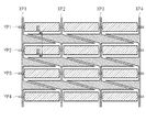
図2はタッチパネル付表示装置100のX電極XP1〜XP4及びY電極YP1〜YP4の形状について示す図である。X電極XP1〜XP4及びY電極YP1〜YP4は、タッチパネル120内に、それぞれ同じ平面内に形成されている。上述したようにX電極XP1〜XP4とY電極YP1〜YP4とは、検出用配線111によって容量検出部102に接続される。Y電極YP1〜YP4はタッチパネル120の長手方向である横方向に伸びており、縦方向に4本並べられている。各電極の交差部分は、各電極の交差容量を削減するために電極幅を細くしている(以下、「細線部」という。)。したがって、Y電極YP1〜YP4はその延在方向に細線部と、それ以外の電極部分(以下、「パット部」という。)とを交互に配置した形状となる。隣接するY電極YP1〜YP4の間に、X電極XP1〜XP4を配置する。X電極XP1〜XP4はタッチパネル120の縦方向に延びており、横方向に4本並べられる。Y電極YP1〜YP4と同様に、X電極XP1〜XP4はその延在方向に細線部とパッド部を交互に配置した形状となる。
FIG. 2 is a diagram illustrating the shapes of the X electrodes XP1 to XP4 and the Y electrodes YP1 to YP4 of the
X電極のパッド部の電極形状は、そのX電極の縦方向中心線に近いほど面積が大きく、隣接するX電極の縦方向中心線に近くなるにつれて面積が小さくなる。例えば、X電極XP2とX電極XP3の場合では、X電極XP2の縦方向中心線付近ではX電極XP2のパッド部の電極面積が最大となり、X電極XP3のパッド部の電極面積は最小となる。一方、X電極XP3の縦方向中心線付近ではX電極XP2のパッド部の電極面積が最小となり、X電極XP3のパッド部の電極面積が最大となる。 The electrode shape of the pad portion of the X electrode increases as it approaches the vertical center line of the X electrode, and decreases as it approaches the vertical center line of the adjacent X electrode. For example, in the case of the X electrode XP2 and the X electrode XP3, the electrode area of the pad portion of the X electrode XP2 is maximized near the longitudinal center line of the X electrode XP2, and the electrode area of the pad portion of the X electrode XP3 is minimized. On the other hand, in the vicinity of the vertical center line of the X electrode XP3, the electrode area of the pad portion of the X electrode XP2 is minimized, and the electrode area of the pad portion of the X electrode XP3 is maximized.
以下の説明において、X電極XP1〜XP4のすべての電極、又はX電極XP1〜XP4のいずれかの電極を、単に「X電極XP」と示し、同様に、Y電極YP1〜YP4のすべての電極、又はY電極YP1〜YP4のいずれかの電極を、単に「Y電極YP」と示す。 In the following description, all the electrodes of the X electrodes XP1 to XP4 or any one of the X electrodes XP1 to XP4 are simply referred to as “X electrodes XP”, and similarly, all the electrodes of the Y electrodes YP1 to YP4, Alternatively, any one of the Y electrodes YP1 to YP4 is simply referred to as “Y electrode YP”.
図3は、図2のIII−III線において、タッチパネル付表示装置100を切断した場合の部分断面図である。なお、この部分断面図では、タッチパネル動作の説明に必要となる層のみ示している。
3 is a partial cross-sectional view of the display device with a
この部分断面図に示されるように、タッチパネル120は、ガラス基板等からなるタッチ基板121と、タッチ基板121に形成された透明導電膜であるX電極XP1及びXP2と、X電極XP1及びXP2を覆うように形成された透明絶縁膜122と、透明絶縁膜122に形成された透明導電膜であるY電極YP2と、Y電極YP2を覆うように形成された透明絶縁膜123と、透明絶縁膜123に形成された複数の非導電性のスペーサ124と、により構成されている。
As shown in this partial cross-sectional view, the
また、表示パネル130は、表示装置部131と、表示装置部131上に形成された透明弾性層132と、後述するZ電極ZPを支持する非導電層133と、表示領域全体を覆うように形成された透明電極であるZ電極ZPと、により構成されている。タッチパネル120と表示パネル130とは、Z電極ZPと、スペーサ124が形成された透明絶縁膜123とが、空気層125を介して対向するように設置されている。
The
次に、タッチパネル120の各層について、詳細に説明する。タッチ基板121の材質、厚さなどは特に限定するものではなく、その用途目的に応じてバリウムホウケイ酸ガラス、ソーダガラスなどの無機ガラス、化学強化ガラスを選択することができ、タッチ基板101の板厚は300μm以下とすることが好ましい。また、板厚500μm程度のガラスを使用して、各層を積層形成し、表示装置と組み合わせてから、研磨砥粒、研磨布を用いた両面研磨や片面研磨法等の機械研磨法でタッチ基板121の板厚を300μmにすることもできる。さらに、弗酸をベースとするエッチング液を用い、さらに浸漬してタッチ基板121の板厚を300μmにすることもできる。タッチ基板121は、ポリエーテルスルホン(PES)、ポリスルホン(PSF)、ポリカーボネート(PC)、ポリアリレート(PAR)、ポリエチレンテレフタレート(PET)などの樹脂フィルム等の中から選ぶこともでき、フィルム厚は必要に応じて適宜選択することができる。
Next, each layer of the
また、X電極XP及びY電極YPに使用する電極は透明導電膜であり、導電性を有する薄膜であれば特に限定するものではなく、従来のITO(酸化インジウム錫)、ATO(酸化アンチモン錫)、IZO(酸化インジウム亜鉛)等を使用することができる。透明導電膜(厚さ50〜200Å)は、表面抵抗が500〜2000Ωになるように、スパッタリング法により成膜、次にレジスト材料を塗布し、露光、現像プロセスによりパターニングする。このときレジスト材料としてはポジ型、ネガ型どちらでもよく、アルカリ現像タイプが容易に形成できる。その後、ITOをエッチングによりパターン形成する。このときのエッチング液は臭化水素酸水溶液等を選択すればよい。 The electrodes used for the X electrode XP and the Y electrode YP are transparent conductive films and are not particularly limited as long as they are conductive thin films. Conventional ITO (indium tin oxide), ATO (antimony tin oxide) IZO (indium zinc oxide) or the like can be used. The transparent conductive film (thickness 50 to 200 mm) is formed by sputtering so that the surface resistance is 500 to 2000Ω, and then a resist material is applied and patterned by exposure and development processes. At this time, the resist material may be either a positive type or a negative type, and an alkali development type can be easily formed. Thereafter, ITO is patterned by etching. As the etching solution at this time, a hydrobromic acid aqueous solution or the like may be selected.
タッチ基板121に近い箇所にX電極XPを形成し、次にX電極XPとY電極YPを絶縁するための透明絶縁膜122を形成する。その次に、Y電極YPを形成する。ここで、X電極XPとY電極YPの順番を入れ換えても良い。Y電極YPの次には透明絶縁膜123を配置し、表示パネル130のZ電極ZPとの絶縁性を確保する。透明絶縁膜122、透明絶縁膜123としては、膜厚は絶縁膜材料の誘電率を考慮すれば各種選択できるが、比誘電率2〜4で調整するのが容易であり、膜厚は1〜20μmで形成することができる。絶縁膜層の材料としては、UV(紫外線)硬化型樹脂材料やアルカリ現像可能なネガまたはポジ型の絶縁膜材料、加熱で硬化する熱硬化型樹脂材料を用いることができるが、アルカリ現像タイプが容易に形成できる。
An X electrode XP is formed at a location close to the
スペーサ124は、光硬化性の樹脂材料からなり、ドット状の柱状スペーサを使用することができる。スクリーン印刷等により、20μm以上、10000μm以下の間隔で形成するのが好ましい。スペーサの形状は円形、四角形等、自由に選択でき、径は5〜100μmの範囲で選択でき、20〜50μmが好ましい。
The
次に、表示パネル130の各層について、詳細に説明する。表示装置部131は、平面表示装置であれば特に制限するものではなく、例えば、液晶表示装置、有機EL(Electro Luminescence)表示装置、及びプラズマ表示装置等が使用でき、通常使用する形態で、表示装置表面に透明弾性層132が接着して使用することができる。
Next, each layer of the
透明弾性層132は、図4に示されるように、硬さと粘着力の異なる3層構造、すなわち表示装置部131側から順に、低硬度透明弾性層151、高硬度透明弾性層152、及び低硬度透明弾性層153で形成される。低硬度透明弾性層151及び153はこれと隣接する層との接着力を保ち、大きな荷重(例えば樹脂ペンで10ニュートン以上)の大きな荷重で繰返し押圧を加えた場合にも塑性変形や接着ずれしない層である。一方、高硬度透明弾性層152に接着力は特に必要なく、弾性が備わり、大きな荷重で繰返し押圧を加えた場合にも塑性変形しない層である。
As shown in FIG. 4, the transparent
低硬度透明弾性層151及び153は、弾性を有するゴム状で粘着力を有する材料であれば特に制限するものではないが、大きな荷重で繰返し押圧を加えた場合にも塑性変形しない材料が好ましい。本発明では、アクリル系粘着材、酢酸ビニル系粘着材、ウレタン系粘着材、エポキシ樹脂、塩化ビニリデン系樹脂、ポリアミド系樹脂、ポリエステル系樹脂、合成ゴム系粘着材、シリコーン系樹脂が挙げられ、この中でも透明性の高いアクリル系粘着材およびシリコーン系樹脂が好ましい。アクリル系粘着材は(メタ)アクリル酸アルキルエステル、(メタ)アクリル酸、(メタ)アクリル酸ヒドロキシアルキルなどの1種あるいは2種以上の混合物を溶液重合法、乳化重合法、塊状重合法、懸濁重合法、UV重合法などの公知の重合法で重合して得られるアクリル系重合体に、必要に応じて粘着付与剤、充填剤等の添加剤を添加することにより得られる。(メタ)アクリル酸アルキルエステルの具体例としては、(メタ)アクリル酸ブチル、(メタ)アクリル酸イソブチル、(メタ)アクリル酸へキシル、(メタ)アクリル酸2−エチルヘキシル、(メタ)アクリル酸イソオクチル、(メタ)アクリル酸イソノニル、(メタ)アクリル酸アリル、(メタ)アクリル酸ラウリル、(メタ)アクリル酸ステアリル等が挙げられる。
The low-hardness transparent
高硬度透明弾性層152は、弾性を有するゴム状の材料であれば特に制限するものではないが、大きな荷重で繰返し押圧を加えた場合にも塑性変形しない材料が好ましい。例えば、ブチルゴム、フッ素ゴム、エチレン-プロピレン-ジエン共重合ゴム(EPDM)、アクリルニトリル−ブタジエンゴム(NBR)、クロロプレンゴム(CR)、天然ゴム(NR)、イソプレンゴム(IR)、スチレン-ブタジエンゴム(SBR)、ブタジエンゴム、エチレン−プロピレンゴム、シリコーンゴム、ポリウレタンゴム、ポリノルボルネンゴム、スチレン−ブタジエン−スチレンゴム、エピクロロヒドリンゴム、NBRの水素化物、多硫化ゴム、ウレタンゴム等のゴムを単独であるいは2種類以上を混合して用いることができる。また、低硬度透明弾性層151及び153と同様に、アクリル系粘着材、酢酸ビニル系粘着材、ウレタン系粘着材、エポキシ樹脂、塩化ビニリデン系樹脂、ポリアミド系樹脂、ポリエステル系樹脂、合成ゴム系粘着材、シリコーン系樹脂を使用することもでき、この中でも透明性の高いアクリル系粘着材およびシリコーン系樹脂が好ましく、低硬度透明弾性層151及び153よりも重合度を高くし、硬くして形成する。
The high-hardness transparent
透明弾性層132の層厚は、高荷重で押圧を加えた場合の変形量を小さくして、隣接する層とのズレを抑制するため、200μm以下で、スペーサの高さより厚くすることが好ましい。低硬度透明弾性層151及び153、高硬度透明弾性層152のそれぞれの層厚は、5〜100μmの範囲で選択できるが、それぞれ40μm以下として、透明弾性層132の層厚を約100μmとすることが好ましい。
The layer thickness of the transparent
非導電層133は、可視光透過率から、ポリエーテルスルホン(PES)、ポリスルホン(PSF)、ポリカーボネート(PC)、ポリアリレート(PAR)、ポリエチレンテレフタレート(PET)などの透明な樹脂フィルム等のようなものの中から選ぶことが好ましい。タッチして押圧が加わったときに透明弾性層132の弾性を抑制せず、非導電層133がスペーサ124の形状に沿って変形する必要があるため、非導電層133は100μm以下が好ましい。
The
Z電極ZPは、透明導電膜であり、導電性を有する薄膜であれば特に限定するものではなく、この薄膜を形成する基材として非導電層133に対して、従来のITO(酸化インジウム錫)、ATO(酸化アンチモン錫)、IZO(酸化インジウム亜鉛)等を使用することができる。透明導電膜は、表面抵抗が500〜2000Ωになるように、スパッタリング法により成膜、次にレジスト材料を塗布し、露光、現像プロセスによりX電極XP、Y電極YPに対応した形状にパターニングする。このときレジスト材料としてはポジ型、ネガ型どちらでもよく、アルカリ現像タイプが容易に形成できる。その後、ITOをエッチングによりパターン形成する。このときのエッチング液は臭化水素酸水溶液等を選択すればよい。また、表面抵抗を10000〜10000000ΩになるようにZ電極ZPを形成するとパターニングは不要となり、従来のITO(酸化インジウム錫)、ATO(酸化アンチモン錫)、IZO(酸化インジウム亜鉛)等の微粒子を透明樹脂に分散させた薄膜のほか、導電性を有する微粒子として、例えばニッケル、金、銀、銅などの金属微粒子のほか、絶縁性の無機微粒子や樹脂微粒子に金属メッキを施したものを樹脂中に分散させたもの等が使用できる。また、Al2O3、Bi2O3、CeO2、In2O3、(In2O3・SnO2)、HfO2、La2O3、MgF2、Sb2O5、(Sb2O5・SnO2)、SiO2、SnO2、TiO2、Y2O3、ZnOおよびZrO2からなる群から少なくとも1種の金属酸化物、または金属フッ化物からなる微粒子も透明樹脂中に分散することで使用できる。また、ポリアニリン、ポリアセチレン、ポリエチレンジオキシチオフェン、ポリピロール、ポリイソチアナフテン、ポリイソナフトチオフェン等の有機導電性材料を塗布して使用することもできる。また、Z電極ZPは光屈折率や光反射による光の吸収や散乱が少ないものが好ましく、適宜選択する事が好ましい。
The Z electrode ZP is a transparent conductive film and is not particularly limited as long as it is a conductive thin film. Conventionally, ITO (indium tin oxide) is used as a base material for forming the thin film with respect to the
図5は、タッチパネル付表示装置100におけるタッチ操作時の容量変化について、説明するための模式図である。タッチ操作の入力手段である入力ペン190は、非導電性であり、タッチ時の押圧によりX電極XP1とZ電極ZPとの距離、及びY電極YP2とZ電極ZPとの距離が変化することにより、容量が変化する。また、指などの導電性の入力手段でも押圧によるX電極XP1とZ電極ZPとの距離、およびY電極YP2とZ電極ZPとの距離が変化すれば同様である。
FIG. 5 is a schematic diagram for explaining a change in capacity during a touch operation in the
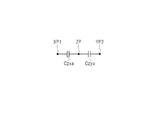
隣接するX電極XP1とY電極YP2間の容量は、絶縁膜を介したX電極XP1とY電極YP2間の容量(図示せず)、X電極XP1とZ電極ZP間の容量、およびY電極YP2とZ電極ZP間の容量がそれぞれ形成する平行平板容量などの合成容量に相当する。ここで、タッチ操作が無い場合のX電極XP1とZ電極間の容量をCzx、Y電極YP2とZ電極間の容量をCzyとし、図5のようにタッチ時の押圧によりZ電極ZPが押し下げられたときのX電極XP1とZ電極ZP間の容量をCzxa、Y電極YP2とZ電極ZP間の容量をCzyaとすると、X電極XP1とZ電極ZPとの距離、及びY電極YPとZ電極ZPとの距離は共に短くなる為、その平行平板容量は大きくなり、次の関係式を満たす。 The capacitance between the adjacent X electrode XP1 and Y electrode YP2 is the capacitance between the X electrode XP1 and Y electrode YP2 (not shown) via the insulating film, the capacitance between the X electrode XP1 and Z electrode ZP, and the Y electrode YP2. And the Z electrode ZP corresponds to a combined capacitance such as a parallel plate capacitance formed respectively. Here, when there is no touch operation, the capacitance between the X electrode XP1 and the Z electrode is Czx, and the capacitance between the Y electrode YP2 and the Z electrode is Czy, and the Z electrode ZP is pushed down by the pressure at the time of touch as shown in FIG. When the capacitance between the X electrode XP1 and the Z electrode ZP is Czxa, and the capacitance between the Y electrode YP2 and the Z electrode ZP is Czya, the distance between the X electrode XP1 and the Z electrode ZP, and the Y electrode YP and the Z electrode ZP The distance between and the parallel plate capacity increases, and the following relational expression is satisfied.

Z電極ZPは電気的にフローティングであるため、図5のタッチ操作有の状態では、合成容量は図6に示すような直列容量と考えられる。したがって、タッチ操作の有無で生じる隣接するX電極とY電極間の容量変化ΔCは、式(3)で表される。 Since the Z electrode ZP is electrically floating, the combined capacitance is considered to be a series capacitance as shown in FIG. Therefore, the capacitance change ΔC between the adjacent X electrode and Y electrode caused by the presence or absence of the touch operation is expressed by Expression (3).
容量検出部102は、各電極の容量又は容量変化ΔCを検出する。制御演算部103は、容量検出部102で得られる各電極の容量又は容量変化ΔCなどを信号成分として、タッチ操作時の座標を計算する。以上のことから、非導電性の入力手段であっても、押圧によりX電極XPとZ電極ZP、およびY電極YPとZ電極ZPの距離が変化することで静電容量変化により入力座標を検知することが可能となる。
The
図7は、タッチパネル付表示装置100の表示領域の端付近の断面図である。通常、表示装置部131の最表面は表示領域139内、または表示領域139より広く偏光フィルムが形成されている。この偏光フィルムと同じ程度の平面方向寸法を有する大きさで、透明弾性層132、非導電層133及びZ電極ZPを順次積層して形成する。表示装置部131の表示領域139の周囲(偏光フィルが貼られていない部分)に固定シール127を形成し、タッチパネル120を固定シール127を介して額縁状に接着固定する。また、このとき偏光フィルム面と固定シール127の接着性が確保されれば、偏光フィルム上に固定シール127を形成しても良い。
FIG. 7 is a cross-sectional view near the edge of the display area of the
固定シール127は、必要なギャップに対応する微粒子等を一定量含有した樹脂材料が使用でき、シリコーン樹脂、ウレタン系樹脂、エポキシ系樹脂、ポリエステル系樹脂、アクリル系樹脂等が挙げられる。この固定シール127の硬化には紫外線、熱、これらの併用することが可能であるが、表示装置部131の耐熱性や非導電性のスペーサ124、導電性の導電層であるZ電極ZP、Z電極ZPを支持する非導電層133、透明弾性層132等の劣化を抑えるため、紫外線硬化型の樹脂が好ましい。固定シール127の接着固定用樹脂材料の塗布方法は、樹脂材料を均一に額縁状に塗布することができる方法であれば特に限定されるものではなく、ディスペンサー塗布、スクリーン印刷塗布等の方法を用いることができる。塗布の幅は、必要な耐久性に応じて選択できるが、500μm〜2000μmが好ましい。
For the fixed
また、固定シール127は、必要なギャップに対応する粘着シートも使用でき、粘着性を有するシート型の粘着材料としては、アクリル系粘着材、酢酸ビニル系粘着材、ウレタン系粘着材、エポキシ樹脂、塩化ビニリデン系樹脂、ポリアミド系樹脂、ポリエステル系樹脂、合成ゴム系粘着材、シリコーン系樹脂が挙げられる。粘着固定時の取り扱い易さから、基材としてポリエチレンテレフタレート(PET)等のフィルムを使用した両面粘着フィルムが好ましく、粘着フィルムの幅は、必要な耐久性に応じて選択できるが、500μm〜3000μmが好ましい。
Moreover, the fixed
したがって、本発明の実施形態によれば、非導電性の入力手段によりタッチパネル上へ接触した場合でも、容量検出用のX電極やY電極と、Z電極との距離が変化することで容量変化を発生できるため、静電容量結合方式として入力座標を検出することが出来る。 Therefore, according to the embodiment of the present invention, even when the touch panel is touched by the non-conductive input means, the capacitance change is caused by the change in the distance between the X electrode or Y electrode for capacitance detection and the Z electrode. Since it can generate | occur | produce, an input coordinate can be detected as a capacitive coupling system.
また、タッチパネルの機能の部品の1つとして表示装置部131の基板を利用しているため、タッチパネル専用の基板が1枚不要となり、表示装置からの光の透過率を向上させることができると共に、表示装置部131にタッチパネルの基板を接着剤や両面粘着フィルム等で接着固定する必要がなく、製造工程及び部品点数の削減により低コストなタッチパネル付き表示装置とすることができる。
In addition, since the substrate of the
[第2実施形態]
本発明の第2実施形態におけるタッチパネル付表示装置200は、タッチパネル220と表示パネル230とを備え、その他の構成は、図1に示した第1実施形態におけるタッチパネル付表示装置100と同様である。
[Second Embodiment]
The display device with a
図8は、タッチパネル220と表示パネル230の構成について、図3と同じ視野で示す断面図である。図8に示されるように、タッチパネル220は、第1実施形態のタッチパネル120と同様に、ガラス基板等からなるタッチ基板221と、タッチ基板221に形成された透明導電膜であるX電極XP1及びXP2と、X電極XP1及びXP2を覆うように形成された透明絶縁膜222と、透明絶縁膜222に形成された透明導電膜であるY電極YP2と、Y電極YP2を覆うように形成された透明絶縁膜223と、透明絶縁膜223に形成された複数の非導電性のスペーサ224と、により構成されている。
FIG. 8 is a cross-sectional view showing the configurations of the
また、表示パネル230は、表示装置部231と、表示装置部231上に形成された透明弾性層232と、後述するZ電極ZPを支持する非導電層233と、表示領域全体を覆うように形成された透明電極であるZ電極ZPと、により構成されている。タッチ基板221と表示パネル230とは、Z電極ZPと透明絶縁膜223とが、スペーサ224によって形成される空気層225を介して対向するように設置されている。
Further, the
スペーサ224を除く各層を構成する材料および特性は第1実施形態と同様であり、説明を省略する。スペーサ224は、粒径がそろったポリマービーズ、ガラスビーズ等を適宜散布して形成する。透明絶縁膜223とZ電極ZPの間隔を規定するビーズの粒径は5〜100μmの範囲で選択でき、20〜50μmが好ましい。散布するビーズの密度は20μm以上、10000μm以下の間隔で散布するのが好ましい。
The materials and characteristics constituting each layer excluding the
図9は、タッチパネル付表示装置200におけるタッチ操作時の容量変化について、説明するための模式図である。第1実施形態のタッチパネル付表示装置100と同様に、タッチ操作の入力手段である入力ペン190は、非導電性であり、タッチ時の押圧によりX電極XPとZ電極ZPとの距離、及びY電極YPとZ電極ZPとの距離が変化することにより、容量が変化する。また、導電性の入力手段(指など)でも押圧により、X電極XPとZ電極ZPとの距離、及びY電極YPとZ電極ZPとの距離が変化すれば同様である。
FIG. 9 is a schematic diagram for explaining a change in capacity at the time of a touch operation in the
タッチパネル付表示装置200におけるタッチ操作時においても、本発明の第1実施形態にて説明した図5と同様に、X電極XPとZ電極ZPとの距離、及びY電極YPとZ電極ZPとの距離が短くなるため、このときの容量変化ΔCは上述した式(3)と同様に表される。容量検出部102は、各電極の容量又は式(3)で表されるような容量変化ΔCを検出する。制御演算部103は、容量検出部で得られる各電極の容量又は容量変化ΔCなどを信号成分として、タッチ操作時の座標を計算する。
Even during a touch operation on the
したがって、本発明の実施形態によれば、第1実施形態と同様に、非導電性の入力手段によりタッチパネル上へ接触した場合でも、容量検出用のX電極やY電極と、Z電極との距離が変化することで容量変化を発生できるため、静電容量結合方式として入力座標を検出することが出来る。 Therefore, according to the embodiment of the present invention, as in the first embodiment, the distance between the X electrode or Y electrode for capacitance detection and the Z electrode even when the non-conductive input means contacts the touch panel. Since the capacitance change can be generated by the change of, the input coordinate can be detected as a capacitive coupling method.
また、タッチパネルの機能の部品の1つとして表示装置部131の基板を利用しているため、タッチパネル専用の基板が1枚不要となり、表示装置からの光の透過率を向上させることができると共に、表示装置部131にタッチパネルの基板を接着剤や両面粘着フィルム等で接着固定する必要がなく、製造工程及び部品点数の削減により低コストでコンパクトなタッチパネル付き表示装置とすることができる。
In addition, since the substrate of the
[第3実施形態]
本発明の第3実施形態におけるタッチパネル付表示装置300は、タッチパネル320と表示パネル330とを備え、その他の構成は、図1に示した第1実施形態におけるタッチパネル付表示装置100と同様である。
[Third Embodiment]
The display device with a
図10は、タッチパネル320と表示パネル330の構成について、図3と同じ視野で示す断面図である。
FIG. 10 is a cross-sectional view showing the configurations of the
図10に示されるように、タッチパネル320は、ガラス基板等からなるタッチ基板321と、タッチ基板321に形成された透明導電膜であるX電極XP1及びXP2と、X電極XP1及びXP2を覆うように形成された透明絶縁膜322と、透明絶縁膜322に形成された透明導電膜であるY電極YP2と、Y電極YP2を覆うように形成された透明絶縁膜323と、透明弾性層327と、Z電極ZPを支持する非導電層328と、表示領域全体を覆うように形成された透明電極であるZ電極ZPと、により構成されている。
As shown in FIG. 10, the
表示パネル330は、表示装置部331と、表示装置部331上に形成されたスペーサ334により構成されている。タッチパネル320と表示パネル330とは、Z電極ZPと表示パネル330とが、スペーサ334によって形成される空気層325を介して対向するように設置されている。
The
スペーサ334を除く各層を構成する材料および特性は第1実施形態と同様であり、説明を省略する。スペーサ334は、光硬化性の樹脂材料からなり、ドット状の柱状スペーサを使用することができる。スクリーン印刷等により、20μm以上、10000μm以下の間隔で形成するのが好ましい。スペーサ334の形状は円形、四角形等、自由に選択でき、径は5〜100μmの範囲で選択でき、20〜50μmが好ましい。
The materials and characteristics constituting each layer excluding the
図11は、タッチパネル付表示装置300におけるタッチ操作時の容量変化について、説明するための模式図である。第1実施形態のタッチパネル付表示装置100と同様に、タッチ操作の入力手段である入力ペン190は、非導電性であり、タッチ時の押圧によりX電極XPとZ電極ZPとの距離、及びY電極YPとZ電極ZPとの距離が変化することにより、容量が変化する。また、導電性の入力手段(指など)でも押圧により、X電極XPとZ電極ZP及びY電極YPとZ電極ZPの距離が変化すれば同様である。
FIG. 11 is a schematic diagram for explaining a change in capacity at the time of a touch operation in the
タッチパネル付表示装置300におけるタッチ操作時においても、本発明の第1実施形態にて説明した図5と同様に、X電極XPとZ電極ZPとの距離、及びY電極YPとZ電極ZPとの距離が短くなるため、このときの容量変化ΔCは上述した式(3)と同様に表される。容量検出部102は、各電極の容量又は式(3)で表されるような容量変化ΔCを検出する。制御演算部103は、容量検出部で得られる各電極の容量又は容量変化ΔCなどを信号成分として、タッチ操作時の座標を計算する。
Similarly to FIG. 5 described in the first embodiment of the present invention, the distance between the X electrode XP and the Z electrode ZP and the distance between the Y electrode YP and the Z electrode ZP are similar to those in FIG. Since the distance is shortened, the capacitance change ΔC at this time is expressed in the same manner as the above-described equation (3). The
したがって、本発明の実施形態によれば、第1実施形態と同様に、非導電性の入力手段によりタッチパネル上へ接触した場合でも、容量検出用のX電極やY電極と、Z電極との距離が変化することで容量変化を発生できるため、静電容量結合方式として入力座標を検出することが出来る。 Therefore, according to the embodiment of the present invention, as in the first embodiment, the distance between the X electrode or Y electrode for capacitance detection and the Z electrode even when the non-conductive input means contacts the touch panel. Since the capacitance change can be generated by the change of, the input coordinate can be detected as a capacitive coupling method.
また、タッチパネルの機能の部品の1つとして表示装置部131の基板を利用しているため、タッチパネル専用の基板が1枚不要となり、表示装置からの光の透過率を向上させることができると共に、表示装置部131にタッチパネルの基板を接着剤や両面粘着フィルム等で接着固定する必要がなく、製造工程及び部品点数の削減により低コストでコンパクトなタッチパネル付き表示装置とすることができる。
In addition, since the substrate of the
[第4実施形態]
本発明の第4実施形態におけるタッチパネル付表示装置400は、タッチパネル420と表示パネル430とを備え、その他の構成は、図1に示した第1実施形態におけるタッチパネル付表示装置100と同様である。
[Fourth Embodiment]
The display device with a
図12は、タッチパネル420と表示パネル430の構成について、図3と同じ視野で示す断面図である。
12 is a cross-sectional view showing the configurations of the
図12に示されるように、タッチパネル420は、ガラス基板等からなるタッチ基板421と、透明導電膜であるX電極XP1及びXP2と、X電極XP1及びXP2を覆うように形成された透明絶縁膜422と、透明絶縁膜422に形成された透明導電膜であるY電極YP2と、Y電極YP2を覆うように形成された透明絶縁膜423と、透明絶縁膜423に形成された透明弾性層427と、透明弾性層427に形成され、Z電極ZPを支持する非導電層428と、非導電層428に表示領域全体を覆うように形成された透明電極であるZ電極ZPと、により構成されている。
As shown in FIG. 12, the
表示パネル430は、表示装置部431と、表示装置部431上に形成されたスペーサ434とにより構成されている。タッチパネル420と表示パネル430とは、Z電極ZPと表示装置部431とが、スペーサ434によって形成される空気層425を介して対向するように設置されている。スペーサ434を除く各層を構成する材料および特性は第1実施形態と同様であり、説明を省略する。
The
スペーサ434は、粒径がそろったポリマービーズ、ガラスビーズ等を適宜散布して形成する。表示装置部431とZ電極ZPとの間隔を規定するビーズの粒径は5〜100μmの範囲で選択でき、20〜50μmが好ましい。散布するビーズの密度は20μm以上、10000μm以下の間隔で散布するのが好ましい。
The
図13は、タッチパネル付表示装置400におけるタッチ操作時の容量変化について、説明するための模式図である。第1実施形態のタッチパネル付表示装置100と同様に、タッチ操作の入力手段である入力ペン190は、非導電性であり、タッチ時の押圧によりX電極XPとZ電極ZPとの距離、及びY電極YPとZ電極ZPとの距離が変化することにより、容量が変化する。また、導電性の入力手段(指など)でも押圧により、X電極XPとZ電極ZPとの距離、及びY電極YPとZ電極ZPとの距離が変化すれば同様である。
FIG. 13 is a schematic diagram for explaining a change in capacity during a touch operation in the
タッチパネル付表示装置400におけるタッチ操作時においても、本発明の第1実施形態にて説明した図5と同様に、X電極XPとZ電極ZPとの距離、及びY電極YPとZ電極ZPとの距離が短くなる。よって、このときの容量変化ΔCは式(3)と同様に表される。容量検出部102は、各電極の容量又は式(3)で表されるような容量変化ΔCを検出する。制御演算部103は、容量検出部で得られる各電極の容量又は容量変化ΔCなどを信号成分として、タッチ操作時の座標を計算する。
Even during a touch operation on the display device with a
したがって、本発明の実施形態によれば、第1実施形態と同様に、非導電性の入力手段によりタッチパネル上へ接触した場合でも、容量検出用のX電極やY電極と、Z電極との距離が変化することで容量変化を発生できるため、静電容量結合方式として入力座標を検出することが出来る。 Therefore, according to the embodiment of the present invention, as in the first embodiment, the distance between the X electrode or Y electrode for capacitance detection and the Z electrode even when the non-conductive input means contacts the touch panel. Since the capacitance change can be generated by the change of, the input coordinate can be detected as a capacitive coupling method.
また、タッチパネルの機能の部品の1つとして表示装置部131の基板を利用しているため、タッチパネル専用の基板が1枚不要となり、表示装置からの光の透過率を向上させることができると共に、表示装置部131にタッチパネルの基板を接着剤や両面粘着フィルム等で接着固定する必要がなく、製造工程及び部品点数の削減により低コストでコンパクトなタッチパネル付き表示装置とすることができる。
In addition, since the substrate of the
100 タッチパネル付表示装置、101 タッチ基板、102 容量検出部、103 制御演算部、104 システム、105 表示制御回路、111 検出用配線、112 容量検出信号、113 検出制御信号、114 インターフェース信号、115 表示信号、116 表示制御信号、120 タッチパネル、121 タッチ基板、122 透明絶縁膜、123 透明絶縁膜、124 スペーサ、125 空気層、127 固定シール、130 表示パネル、131 表示装置部、132 透明弾性層、133 非導電層、139 表示領域、151 低硬度透明弾性層、152 高硬度透明弾性層、153 低硬度透明弾性層、190 入力ペン、200 タッチパネル付表示装置、220 タッチパネル、221 タッチ基板、222 透明絶縁膜、223 透明絶縁膜、224 スペーサ、225 空気層、230 表示パネル、231 表示装置部、232 透明弾性層、233 非導電層、300 タッチパネル付表示装置、320 タッチパネル、321 タッチ基板、322 透明絶縁膜、323 透明絶縁膜、325 空気層、327 透明弾性層、328 非導電層、330 表示パネル、331 表示装置部、334 スペーサ、400 タッチパネル付表示装置、420 タッチパネル、421 タッチ基板、422 透明絶縁膜、423 透明絶縁膜、425 空気層、427 透明弾性層、428 非導電層、430 表示パネル、431 表示装置部、434 スペーサ。 DESCRIPTION OF SYMBOLS 100 Display apparatus with a touch panel, 101 Touch substrate, 102 Capacity | capacitance detection part, 103 Control calculation part, 104 system, 105 Display control circuit, 111 Detection wiring, 112 Capacity detection signal, 113 Detection control signal, 114 Interface signal, 115 Display signal 116 Display control signal, 120 Touch panel, 121 Touch substrate, 122 Transparent insulating film, 123 Transparent insulating film, 124 Spacer, 125 Air layer, 127 Fixed seal, 130 Display panel, 131 Display unit, 132 Transparent elastic layer, 133 Non Conductive layer, 139 display area, 151 low hardness transparent elastic layer, 152 high hardness transparent elastic layer, 153 low hardness transparent elastic layer, 190 input pen, 200 display device with touch panel, 220 touch panel, 221 touch substrate, 222 transparent insulating film, 223 transparent insulating film, 224 spacer, 225 air layer, 230 display panel, 231 display device unit, 232 transparent elastic layer, 233 non-conductive layer, 300 display device with touch panel, 320 touch panel, 321 touch substrate, 322 transparent insulating film, 323 Transparent insulating film, 325 air layer, 327 transparent elastic layer, 328 non-conductive layer, 330 display panel, 331 display unit, 334 spacer, 400 display device with touch panel, 420 touch panel, 421 touch substrate, 422 transparent insulating film, 423 transparent Insulating film, 425 air layer, 427 transparent elastic layer, 428 non-conductive layer, 430 display panel, 431 display unit, 434 spacer.
Claims (9)
前記表示パネルの前面側に設けられたタッチパネルと、を備え、
前記タッチパネルは、座標検出用電極を有し、
前記タッチパネルと前記表示パネルとのいずれか一方のパネルには、前記座標検出用電極よりも前記表示パネル側に、前記表示面の表示領域を覆うように配置された導電膜を有し、
前記座標検出用電極と前記表示面との間には、空間が形成されるように配置された複数の非導電性のスペーサを有し、
前記一方のパネルは、
前記導電膜に接する非導電層と、
前記非導電層の、前記導電膜とは反対側の面に配置された透明弾性層と、を更に有し、
前記他方のパネルに配置された前記スペーサは、前記接触面における外部からの接触により、前記導電膜及び前記非導電層を介し、前記透明弾性層を変形させる、ことを特徴とするタッチパネル付表示装置。 A display panel having a display surface;
A touch panel provided on the front side of the display panel,
The touch panel has coordinate detection electrodes,
On one of the panel of the touch panel and the display panel, the said display panel side of the coordinate detection electrodes, have a arranged conductive film so as to cover the display area of the display surface,
Between the coordinate detection electrode and the display surface, having a plurality of non-conductive spacers arranged so as to form a space,
The one panel is
A non-conductive layer in contact with the conductive film;
A transparent elastic layer disposed on a surface of the non-conductive layer opposite to the conductive film;
The display device with a touch panel, wherein the spacer disposed on the other panel deforms the transparent elastic layer through the conductive film and the non-conductive layer by external contact on the contact surface. .
一方向に伸び、外部から接触される接触面と平行な複数の電極であるX電極と、
前記X電極とは異なる層で、前記接触面に垂直な方向に投影した際に前記X方向に垂直な方向に伸び、前記接触面と平行な複数の電極であるY電極と、を備える、ことを特徴とする請求項1に記載のタッチパネル付表示装置。 The coordinate detection electrode is
X electrodes that are a plurality of electrodes extending in one direction and parallel to the contact surface that is contacted from the outside;
A Y electrode that is a layer different from the X electrode, extends in a direction perpendicular to the X direction when projected in a direction perpendicular to the contact surface, and is a plurality of electrodes parallel to the contact surface. The display device with a touch panel according to claim 1.
前記3つの層のうち中央に配置される中間層は、前記中間層の両側に配置される他の2つの層より剛性が高い、ことを特徴とする請求項1乃至3のいずれか一項に記載のタッチパネル付表示装置。 The transparent elastic layer has three layers,
The intermediate layer which is arranged at the center of the three layers, the rigid than the other two layers disposed on opposite sides of the intermediate layer is high, it in any one of claims 1 to 3, wherein The display device with a touch panel as described.
前記スペーサは、前記座標検出用電極と前記導電膜との間に設けられていることを特徴とするタッチパネル付表示装置。 The display device with a touch panel according to any one of claims 1 to 7 ,
The display device with a touch panel, wherein the spacer is provided between the coordinate detection electrode and the conductive film.
前記導電膜は、前記タッチパネルに設けられ、
前記スペーサは、前記導電膜と前記表示面との間に設けられていることを特徴とするタッチパネル付表示装置。 The display device with a touch panel according to any one of claims 1 to 8 ,
The conductive film is provided on the touch panel,
The display device with a touch panel, wherein the spacer is provided between the conductive film and the display surface.
Priority Applications (1)
| Application Number | Priority Date | Filing Date | Title |
|---|---|---|---|
| JP2010040086A JP5520633B2 (en) | 2010-02-25 | 2010-02-25 | Display device with touch panel |
Applications Claiming Priority (1)
| Application Number | Priority Date | Filing Date | Title |
|---|---|---|---|
| JP2010040086A JP5520633B2 (en) | 2010-02-25 | 2010-02-25 | Display device with touch panel |
Publications (3)
| Publication Number | Publication Date |
|---|---|
| JP2011175528A JP2011175528A (en) | 2011-09-08 |
| JP2011175528A5 JP2011175528A5 (en) | 2013-01-17 |
| JP5520633B2 true JP5520633B2 (en) | 2014-06-11 |
Family
ID=44688318
Family Applications (1)
| Application Number | Title | Priority Date | Filing Date |
|---|---|---|---|
| JP2010040086A Active JP5520633B2 (en) | 2010-02-25 | 2010-02-25 | Display device with touch panel |
Country Status (1)
| Country | Link |
|---|---|
| JP (1) | JP5520633B2 (en) |
Families Citing this family (10)
| Publication number | Priority date | Publication date | Assignee | Title |
|---|---|---|---|---|
| JP5255486B2 (en) * | 2009-03-06 | 2013-08-07 | 株式会社ジャパンディスプレイイースト | Display device with input function |
| JP6119518B2 (en) | 2013-02-12 | 2017-04-26 | ソニー株式会社 | Sensor device, input device and electronic apparatus |
| JP6269789B2 (en) * | 2013-02-12 | 2018-01-31 | ソニー株式会社 | Sensor device, input device and electronic apparatus |
| CN105009045B (en) * | 2013-03-13 | 2018-10-12 | 索尼公司 | Sensor device, input unit and electronic equipment |
| US10055067B2 (en) | 2013-03-18 | 2018-08-21 | Sony Corporation | Sensor device, input device, and electronic apparatus |
| JP6142745B2 (en) | 2013-09-10 | 2017-06-07 | ソニー株式会社 | Sensor device, input device and electronic apparatus |
| JP2015190859A (en) | 2014-03-28 | 2015-11-02 | ソニー株式会社 | Sensor device, input device, and electronic apparatus |
| WO2015159914A1 (en) * | 2014-04-16 | 2015-10-22 | 信越ポリマー株式会社 | Capacitive three-dimensional sensor |
| JP6202750B2 (en) * | 2014-04-16 | 2017-09-27 | 信越ポリマー株式会社 | Capacitance type 3D sensor |
| JP2016115178A (en) * | 2014-12-16 | 2016-06-23 | 信越ポリマー株式会社 | Flexible laminate, manufacturing method thereof, and capacitive three-dimensional sensor |
Family Cites Families (8)
| Publication number | Priority date | Publication date | Assignee | Title |
|---|---|---|---|---|
| JPH0784704A (en) * | 1993-09-10 | 1995-03-31 | Fujitsu Ltd | Pressure sensitive input panel |
| JP3277896B2 (en) * | 1998-07-31 | 2002-04-22 | ぺんてる株式会社 | Capacitance coordinate detection device that also serves as pressure detection |
| JP2004045178A (en) * | 2002-07-11 | 2004-02-12 | Nitta Ind Corp | Capacitance type sensor |
| JP2007034736A (en) * | 2005-07-27 | 2007-02-08 | Sharp Corp | Display device with touch panel |
| JP5345336B2 (en) * | 2008-04-15 | 2013-11-20 | 株式会社ジャパンディスプレイ | Input device and display device including the same |
| JP2010015412A (en) * | 2008-07-04 | 2010-01-21 | Hitachi Displays Ltd | Display device equipped with touch panel |
| JP5123774B2 (en) * | 2008-07-25 | 2013-01-23 | 株式会社ジャパンディスプレイイースト | Input device and display device including the same |
| JP5376446B2 (en) * | 2009-07-24 | 2013-12-25 | 株式会社ジャパンディスプレイ | Capacitance type input device and display device with input function |
-
2010
- 2010-02-25 JP JP2010040086A patent/JP5520633B2/en active Active
Also Published As
| Publication number | Publication date |
|---|---|
| JP2011175528A (en) | 2011-09-08 |
Similar Documents
| Publication | Publication Date | Title |
|---|---|---|
| JP5520633B2 (en) | Display device with touch panel | |
| JP5403815B2 (en) | Input device and display device including the same | |
| JP5100738B2 (en) | Input device and display device including the same | |
| JP5039747B2 (en) | Input device and display device including the same | |
| JP5346769B2 (en) | Touch panel and display device including the same | |
| US10234987B2 (en) | Electrode sheet and touch input device | |
| JP5496851B2 (en) | Touch panel | |
| JP5623894B2 (en) | Touch panel | |
| JP5563417B2 (en) | Display device with touch panel | |
| JP5685411B2 (en) | Touch panel | |
| US20100271328A1 (en) | Input device and display device having the same | |
| JP2012084025A (en) | Display device with touch panel | |
| US20170160854A1 (en) | Touch and pressure sensitive panel | |
| JP2011048541A (en) | Touch panel-equipped display device | |
| JP2017068830A (en) | Touch display device | |
| JP2013242635A (en) | Display device with touch panel and display element | |
| KR20120039884A (en) | Touch screen panel and fabricating method for the same | |
| JP2015084148A (en) | Touch type information input image display device and information equipment | |
| KR102008736B1 (en) | Touch panel and method for driving the same | |
| KR20110047529A (en) | Touch panel and touch panel apparatus including the same |
Legal Events
| Date | Code | Title | Description |
|---|---|---|---|
| A521 | Request for written amendment filed |
Free format text: JAPANESE INTERMEDIATE CODE: A523 Effective date: 20121122 |
|
| A621 | Written request for application examination |
Free format text: JAPANESE INTERMEDIATE CODE: A621 Effective date: 20121122 |
|
| A977 | Report on retrieval |
Free format text: JAPANESE INTERMEDIATE CODE: A971007 Effective date: 20130612 |
|
| A131 | Notification of reasons for refusal |
Free format text: JAPANESE INTERMEDIATE CODE: A131 Effective date: 20130618 |
|
| A521 | Request for written amendment filed |
Free format text: JAPANESE INTERMEDIATE CODE: A523 Effective date: 20130801 |
|
| TRDD | Decision of grant or rejection written | ||
| A01 | Written decision to grant a patent or to grant a registration (utility model) |
Free format text: JAPANESE INTERMEDIATE CODE: A01 Effective date: 20140318 |
|
| A61 | First payment of annual fees (during grant procedure) |
Free format text: JAPANESE INTERMEDIATE CODE: A61 Effective date: 20140407 |
|
| R150 | Certificate of patent or registration of utility model |
Ref document number: 5520633 Country of ref document: JP Free format text: JAPANESE INTERMEDIATE CODE: R150 |
|
| R250 | Receipt of annual fees |
Free format text: JAPANESE INTERMEDIATE CODE: R250 |
|
| R250 | Receipt of annual fees |
Free format text: JAPANESE INTERMEDIATE CODE: R250 |
|
| R250 | Receipt of annual fees |
Free format text: JAPANESE INTERMEDIATE CODE: R250 |
|
| R250 | Receipt of annual fees |
Free format text: JAPANESE INTERMEDIATE CODE: R250 |
|
| R250 | Receipt of annual fees |
Free format text: JAPANESE INTERMEDIATE CODE: R250 |
|
| R250 | Receipt of annual fees |
Free format text: JAPANESE INTERMEDIATE CODE: R250 |
|
| R250 | Receipt of annual fees |
Free format text: JAPANESE INTERMEDIATE CODE: R250 |
|
| S111 | Request for change of ownership or part of ownership |
Free format text: JAPANESE INTERMEDIATE CODE: R313117 |
|
| R350 | Written notification of registration of transfer |
Free format text: JAPANESE INTERMEDIATE CODE: R350 |
|
| R250 | Receipt of annual fees |
Free format text: JAPANESE INTERMEDIATE CODE: R250 |
|
| S111 | Request for change of ownership or part of ownership |
Free format text: JAPANESE INTERMEDIATE CODE: R313113 |