JP5516319B2 - Illumination device and display device - Google Patents
Illumination device and display device Download PDFInfo
- Publication number
- JP5516319B2 JP5516319B2 JP2010235925A JP2010235925A JP5516319B2 JP 5516319 B2 JP5516319 B2 JP 5516319B2 JP 2010235925 A JP2010235925 A JP 2010235925A JP 2010235925 A JP2010235925 A JP 2010235925A JP 5516319 B2 JP5516319 B2 JP 5516319B2
- Authority
- JP
- Japan
- Prior art keywords
- electrode
- light
- light source
- guide plate
- light guide
- Prior art date
- Legal status (The legal status is an assumption and is not a legal conclusion. Google has not performed a legal analysis and makes no representation as to the accuracy of the status listed.)
- Expired - Fee Related
Links
Images


Classifications
-
- G—PHYSICS
- G02—OPTICS
- G02F—OPTICAL DEVICES OR ARRANGEMENTS FOR THE CONTROL OF LIGHT BY MODIFICATION OF THE OPTICAL PROPERTIES OF THE MEDIA OF THE ELEMENTS INVOLVED THEREIN; NON-LINEAR OPTICS; FREQUENCY-CHANGING OF LIGHT; OPTICAL LOGIC ELEMENTS; OPTICAL ANALOGUE/DIGITAL CONVERTERS
- G02F1/00—Devices or arrangements for the control of the intensity, colour, phase, polarisation or direction of light arriving from an independent light source, e.g. switching, gating or modulating; Non-linear optics
- G02F1/01—Devices or arrangements for the control of the intensity, colour, phase, polarisation or direction of light arriving from an independent light source, e.g. switching, gating or modulating; Non-linear optics for the control of the intensity, phase, polarisation or colour
- G02F1/13—Devices or arrangements for the control of the intensity, colour, phase, polarisation or direction of light arriving from an independent light source, e.g. switching, gating or modulating; Non-linear optics for the control of the intensity, phase, polarisation or colour based on liquid crystals, e.g. single liquid crystal display cells
- G02F1/133—Constructional arrangements; Operation of liquid crystal cells; Circuit arrangements
- G02F1/1333—Constructional arrangements; Manufacturing methods
- G02F1/1335—Structural association of cells with optical devices, e.g. polarisers or reflectors
- G02F1/1336—Illuminating devices
- G02F1/133615—Edge-illuminating devices, i.e. illuminating from the side
-
- G—PHYSICS
- G02—OPTICS
- G02B—OPTICAL ELEMENTS, SYSTEMS OR APPARATUS
- G02B6/00—Light guides; Structural details of arrangements comprising light guides and other optical elements, e.g. couplings
- G02B6/0001—Light guides; Structural details of arrangements comprising light guides and other optical elements, e.g. couplings specially adapted for lighting devices or systems
- G02B6/0011—Light guides; Structural details of arrangements comprising light guides and other optical elements, e.g. couplings specially adapted for lighting devices or systems the light guides being planar or of plate-like form
- G02B6/0013—Means for improving the coupling-in of light from the light source into the light guide
-
- G—PHYSICS
- G02—OPTICS
- G02B—OPTICAL ELEMENTS, SYSTEMS OR APPARATUS
- G02B6/00—Light guides; Structural details of arrangements comprising light guides and other optical elements, e.g. couplings
- G02B6/0001—Light guides; Structural details of arrangements comprising light guides and other optical elements, e.g. couplings specially adapted for lighting devices or systems
- G02B6/0011—Light guides; Structural details of arrangements comprising light guides and other optical elements, e.g. couplings specially adapted for lighting devices or systems the light guides being planar or of plate-like form
- G02B6/0033—Means for improving the coupling-out of light from the light guide
- G02B6/0035—Means for improving the coupling-out of light from the light guide provided on the surface of the light guide or in the bulk of it
- G02B6/0036—2-D arrangement of prisms, protrusions, indentations or roughened surfaces
-
- G—PHYSICS
- G02—OPTICS
- G02F—OPTICAL DEVICES OR ARRANGEMENTS FOR THE CONTROL OF LIGHT BY MODIFICATION OF THE OPTICAL PROPERTIES OF THE MEDIA OF THE ELEMENTS INVOLVED THEREIN; NON-LINEAR OPTICS; FREQUENCY-CHANGING OF LIGHT; OPTICAL LOGIC ELEMENTS; OPTICAL ANALOGUE/DIGITAL CONVERTERS
- G02F1/00—Devices or arrangements for the control of the intensity, colour, phase, polarisation or direction of light arriving from an independent light source, e.g. switching, gating or modulating; Non-linear optics
- G02F1/01—Devices or arrangements for the control of the intensity, colour, phase, polarisation or direction of light arriving from an independent light source, e.g. switching, gating or modulating; Non-linear optics for the control of the intensity, phase, polarisation or colour
- G02F1/13—Devices or arrangements for the control of the intensity, colour, phase, polarisation or direction of light arriving from an independent light source, e.g. switching, gating or modulating; Non-linear optics for the control of the intensity, phase, polarisation or colour based on liquid crystals, e.g. single liquid crystal display cells
- G02F1/133—Constructional arrangements; Operation of liquid crystal cells; Circuit arrangements
- G02F1/1333—Constructional arrangements; Manufacturing methods
- G02F1/1343—Electrodes
- G02F1/134309—Electrodes characterised by their geometrical arrangement
-
- G—PHYSICS
- G09—EDUCATION; CRYPTOGRAPHY; DISPLAY; ADVERTISING; SEALS
- G09G—ARRANGEMENTS OR CIRCUITS FOR CONTROL OF INDICATING DEVICES USING STATIC MEANS TO PRESENT VARIABLE INFORMATION
- G09G3/00—Control arrangements or circuits, of interest only in connection with visual indicators other than cathode-ray tubes
- G09G3/20—Control arrangements or circuits, of interest only in connection with visual indicators other than cathode-ray tubes for presentation of an assembly of a number of characters, e.g. a page, by composing the assembly by combination of individual elements arranged in a matrix no fixed position being assigned to or needed to be assigned to the individual characters or partial characters
- G09G3/34—Control arrangements or circuits, of interest only in connection with visual indicators other than cathode-ray tubes for presentation of an assembly of a number of characters, e.g. a page, by composing the assembly by combination of individual elements arranged in a matrix no fixed position being assigned to or needed to be assigned to the individual characters or partial characters by control of light from an independent source
- G09G3/3406—Control of illumination source
- G09G3/342—Control of illumination source using several illumination sources separately controlled corresponding to different display panel areas, e.g. along one dimension such as lines
-
- G—PHYSICS
- G02—OPTICS
- G02B—OPTICAL ELEMENTS, SYSTEMS OR APPARATUS
- G02B6/00—Light guides; Structural details of arrangements comprising light guides and other optical elements, e.g. couplings
- G02B6/0001—Light guides; Structural details of arrangements comprising light guides and other optical elements, e.g. couplings specially adapted for lighting devices or systems
- G02B6/0011—Light guides; Structural details of arrangements comprising light guides and other optical elements, e.g. couplings specially adapted for lighting devices or systems the light guides being planar or of plate-like form
- G02B6/0013—Means for improving the coupling-in of light from the light source into the light guide
- G02B6/0023—Means for improving the coupling-in of light from the light source into the light guide provided by one optical element, or plurality thereof, placed between the light guide and the light source, or around the light source
- G02B6/0028—Light guide, e.g. taper
-
- G—PHYSICS
- G02—OPTICS
- G02B—OPTICAL ELEMENTS, SYSTEMS OR APPARATUS
- G02B6/00—Light guides; Structural details of arrangements comprising light guides and other optical elements, e.g. couplings
- G02B6/0001—Light guides; Structural details of arrangements comprising light guides and other optical elements, e.g. couplings specially adapted for lighting devices or systems
- G02B6/0011—Light guides; Structural details of arrangements comprising light guides and other optical elements, e.g. couplings specially adapted for lighting devices or systems the light guides being planar or of plate-like form
- G02B6/0033—Means for improving the coupling-out of light from the light guide
- G02B6/0035—Means for improving the coupling-out of light from the light guide provided on the surface of the light guide or in the bulk of it
- G02B6/0038—Linear indentations or grooves, e.g. arc-shaped grooves or meandering grooves, extending over the full length or width of the light guide
-
- G—PHYSICS
- G02—OPTICS
- G02B—OPTICAL ELEMENTS, SYSTEMS OR APPARATUS
- G02B6/00—Light guides; Structural details of arrangements comprising light guides and other optical elements, e.g. couplings
- G02B6/0001—Light guides; Structural details of arrangements comprising light guides and other optical elements, e.g. couplings specially adapted for lighting devices or systems
- G02B6/0011—Light guides; Structural details of arrangements comprising light guides and other optical elements, e.g. couplings specially adapted for lighting devices or systems the light guides being planar or of plate-like form
- G02B6/0033—Means for improving the coupling-out of light from the light guide
- G02B6/0035—Means for improving the coupling-out of light from the light guide provided on the surface of the light guide or in the bulk of it
- G02B6/004—Scattering dots or dot-like elements, e.g. microbeads, scattering particles, nanoparticles
- G02B6/0041—Scattering dots or dot-like elements, e.g. microbeads, scattering particles, nanoparticles provided in the bulk of the light guide
-
- G—PHYSICS
- G02—OPTICS
- G02B—OPTICAL ELEMENTS, SYSTEMS OR APPARATUS
- G02B6/00—Light guides; Structural details of arrangements comprising light guides and other optical elements, e.g. couplings
- G02B6/0001—Light guides; Structural details of arrangements comprising light guides and other optical elements, e.g. couplings specially adapted for lighting devices or systems
- G02B6/0011—Light guides; Structural details of arrangements comprising light guides and other optical elements, e.g. couplings specially adapted for lighting devices or systems the light guides being planar or of plate-like form
- G02B6/0033—Means for improving the coupling-out of light from the light guide
- G02B6/0035—Means for improving the coupling-out of light from the light guide provided on the surface of the light guide or in the bulk of it
- G02B6/004—Scattering dots or dot-like elements, e.g. microbeads, scattering particles, nanoparticles
- G02B6/0043—Scattering dots or dot-like elements, e.g. microbeads, scattering particles, nanoparticles provided on the surface of the light guide
-
- G—PHYSICS
- G02—OPTICS
- G02B—OPTICAL ELEMENTS, SYSTEMS OR APPARATUS
- G02B6/00—Light guides; Structural details of arrangements comprising light guides and other optical elements, e.g. couplings
- G02B6/0001—Light guides; Structural details of arrangements comprising light guides and other optical elements, e.g. couplings specially adapted for lighting devices or systems
- G02B6/0011—Light guides; Structural details of arrangements comprising light guides and other optical elements, e.g. couplings specially adapted for lighting devices or systems the light guides being planar or of plate-like form
- G02B6/0033—Means for improving the coupling-out of light from the light guide
- G02B6/0058—Means for improving the coupling-out of light from the light guide varying in density, size, shape or depth along the light guide
-
- G—PHYSICS
- G02—OPTICS
- G02F—OPTICAL DEVICES OR ARRANGEMENTS FOR THE CONTROL OF LIGHT BY MODIFICATION OF THE OPTICAL PROPERTIES OF THE MEDIA OF THE ELEMENTS INVOLVED THEREIN; NON-LINEAR OPTICS; FREQUENCY-CHANGING OF LIGHT; OPTICAL LOGIC ELEMENTS; OPTICAL ANALOGUE/DIGITAL CONVERTERS
- G02F1/00—Devices or arrangements for the control of the intensity, colour, phase, polarisation or direction of light arriving from an independent light source, e.g. switching, gating or modulating; Non-linear optics
- G02F1/01—Devices or arrangements for the control of the intensity, colour, phase, polarisation or direction of light arriving from an independent light source, e.g. switching, gating or modulating; Non-linear optics for the control of the intensity, phase, polarisation or colour
- G02F1/13—Devices or arrangements for the control of the intensity, colour, phase, polarisation or direction of light arriving from an independent light source, e.g. switching, gating or modulating; Non-linear optics for the control of the intensity, phase, polarisation or colour based on liquid crystals, e.g. single liquid crystal display cells
- G02F1/133—Constructional arrangements; Operation of liquid crystal cells; Circuit arrangements
- G02F1/1333—Constructional arrangements; Manufacturing methods
- G02F1/1334—Constructional arrangements; Manufacturing methods based on polymer dispersed liquid crystals, e.g. microencapsulated liquid crystals
-
- G—PHYSICS
- G02—OPTICS
- G02F—OPTICAL DEVICES OR ARRANGEMENTS FOR THE CONTROL OF LIGHT BY MODIFICATION OF THE OPTICAL PROPERTIES OF THE MEDIA OF THE ELEMENTS INVOLVED THEREIN; NON-LINEAR OPTICS; FREQUENCY-CHANGING OF LIGHT; OPTICAL LOGIC ELEMENTS; OPTICAL ANALOGUE/DIGITAL CONVERTERS
- G02F1/00—Devices or arrangements for the control of the intensity, colour, phase, polarisation or direction of light arriving from an independent light source, e.g. switching, gating or modulating; Non-linear optics
- G02F1/01—Devices or arrangements for the control of the intensity, colour, phase, polarisation or direction of light arriving from an independent light source, e.g. switching, gating or modulating; Non-linear optics for the control of the intensity, phase, polarisation or colour
- G02F1/13—Devices or arrangements for the control of the intensity, colour, phase, polarisation or direction of light arriving from an independent light source, e.g. switching, gating or modulating; Non-linear optics for the control of the intensity, phase, polarisation or colour based on liquid crystals, e.g. single liquid crystal display cells
- G02F1/133—Constructional arrangements; Operation of liquid crystal cells; Circuit arrangements
- G02F1/1333—Constructional arrangements; Manufacturing methods
- G02F1/1335—Structural association of cells with optical devices, e.g. polarisers or reflectors
- G02F1/1336—Illuminating devices
- G02F1/133601—Illuminating devices for spatial active dimming
-
- G—PHYSICS
- G02—OPTICS
- G02F—OPTICAL DEVICES OR ARRANGEMENTS FOR THE CONTROL OF LIGHT BY MODIFICATION OF THE OPTICAL PROPERTIES OF THE MEDIA OF THE ELEMENTS INVOLVED THEREIN; NON-LINEAR OPTICS; FREQUENCY-CHANGING OF LIGHT; OPTICAL LOGIC ELEMENTS; OPTICAL ANALOGUE/DIGITAL CONVERTERS
- G02F1/00—Devices or arrangements for the control of the intensity, colour, phase, polarisation or direction of light arriving from an independent light source, e.g. switching, gating or modulating; Non-linear optics
- G02F1/01—Devices or arrangements for the control of the intensity, colour, phase, polarisation or direction of light arriving from an independent light source, e.g. switching, gating or modulating; Non-linear optics for the control of the intensity, phase, polarisation or colour
- G02F1/13—Devices or arrangements for the control of the intensity, colour, phase, polarisation or direction of light arriving from an independent light source, e.g. switching, gating or modulating; Non-linear optics for the control of the intensity, phase, polarisation or colour based on liquid crystals, e.g. single liquid crystal display cells
- G02F1/133—Constructional arrangements; Operation of liquid crystal cells; Circuit arrangements
- G02F1/1333—Constructional arrangements; Manufacturing methods
- G02F1/1343—Electrodes
- G02F1/134309—Electrodes characterised by their geometrical arrangement
- G02F1/134318—Electrodes characterised by their geometrical arrangement having a patterned common electrode
Description
本発明は、光に対して散乱性または透明性を示す光変調素子を備えた照明装置および表示装置に関する。 The present invention relates to an illuminating device and a display device including a light modulation element that exhibits scattering or transparency with respect to light.
近年、液晶ディスプレイの高画質化や省エネ化が急進展し、部分的にバックライトの光強度を変調することによって暗所コントラストの向上を実現する方式が提案されている。この手法は主に、バックライトの光源として用いられる発光ダイオード(LED;Light Emitting Diode)を部分的に駆動して、表示画像に合わせてバックライト光を変調するものである。また、大型の液晶ディスプレイにおいて、小型の液晶ディスプレイと同様、薄型化の要求が強まってきており、冷陰極管(CCFL;Cold Cathode Fluorescent Lamp)やLEDを液晶パネルの直下に配置する方式ではなく、導光板の端部に光源を配置するエッジライト方式が注目されている。しかし、エッジライト方式では、光源の光強度を部分的に変調する部分駆動を行うことは難しい。 In recent years, image quality and energy saving of liquid crystal displays have been rapidly advanced, and a method for realizing improvement in contrast in a dark place by partially modulating the light intensity of a backlight has been proposed. This method mainly drives a light emitting diode (LED) used as a light source of the backlight to modulate the backlight light according to the display image. In addition, as with small liquid crystal displays, large liquid crystal displays are becoming increasingly demanding for thinning, and are not a method of arranging a cold cathode fluorescent lamp (CCFL) or LED directly under the liquid crystal panel. An edge light system in which a light source is arranged at the end of a light guide plate has attracted attention. However, in the edge light system, it is difficult to perform partial driving that partially modulates the light intensity of the light source.
ところで、導光板内を伝播している光の取り出し技術としては、例えば、特許文献1において、透明と散乱を切り換える高分子分散液晶(PDLC;Polymer Dispersed Liquid Crystal)を用いた表示装置が提案されている。これは、写り込み防止などを目的としたものであり、PDLCに対して部分的に電圧を印加して、透明と散乱を切り換える技術である。しかし、この方式において、部分的に導光光を取り出すことで、部分的に照明光を変調した場合に、PDLCを駆動する電極パターンに由来する境界部分において輝度の差が大きいときには、表示画像にその境界部分が見えてしまうという問題があった。
By the way, as a technique for extracting light propagating through the light guide plate, for example,
明暗の境界部分をぼかす技術は、例えば特許文献2などに開示されている。これらは、拡散板を使用したり、空間距離を大きくしたりすることで、境界部分の明暗差をぼかそうとするものである。しかし、これらの技術を、PDLCを用いた照明装置に適用した場合には、薄型化が阻害されてしまうという問題がある。
A technique for blurring a bright and dark boundary part is disclosed in, for example,
本発明はかかる問題点に鑑みてなされたもので、その目的は、薄型化を阻害することなく、照明光における明暗の境界部分をぼかすことの可能な照明装置および表示装置を提供することにある。 The present invention has been made in view of such problems, and an object of the present invention is to provide an illumination device and a display device capable of blurring a bright and dark boundary portion in illumination light without inhibiting thinning. .
本発明の照明装置は、導光板と、導光板の側面に配置された光源と、導光板の表面または内部に配置されると共に導光板と接着された光変調素子とを備えたものである。上記の導光板は、当該導光板の側面のうち光源と対向する面の法線と平行な方向に延在する複数の凸部を有している。光源は、互いに独立駆動可能な複数の光源ブロックからなる。また、上記の光変調素子は、離間して互いに対向配置された一対の透明基板と、一対の透明基板の一方の透明基板の表面に設けられ、かつ凸部の延在方向と交差する方向に延在する複数の第1電極と、一対の透明基板の他方の透明基板の表面に設けられた第2電極と、一対の透明基板の間隙に設けられ、かつ電場の大きさに応じて、光源からの光に対して散乱性もしくは透明性を示す光変調層とを有している。 The illuminating device of the present invention includes a light guide plate, a light source disposed on a side surface of the light guide plate, and a light modulation element that is disposed on or inside the light guide plate and bonded to the light guide plate. The light guide plate has a plurality of convex portions extending in a direction parallel to the normal line of the surface facing the light source among the side surfaces of the light guide plate. The light source is composed of a plurality of light source blocks that can be driven independently of each other. In addition, the light modulation element is provided on a surface of a pair of transparent substrates spaced apart from each other and one transparent substrate of the pair of transparent substrates, and in a direction intersecting with the extending direction of the convex portion. A plurality of first electrodes extending, a second electrode provided on the surface of the other transparent substrate of the pair of transparent substrates, and a light source provided in a gap between the pair of transparent substrates and according to the magnitude of the electric field And a light modulation layer exhibiting scattering or transparency with respect to the light from the light.
本発明の表示装置は、マトリクス状に配置された複数の画素を有すると共に、複数の画素が画像信号に基づいて駆動される表示パネルと、表示パネルを照明する照明装置とを備えたものである。この表示装置に搭載された照明装置は、上記の照明装置と同一の構成要素を有している。 The display device of the present invention includes a plurality of pixels arranged in a matrix, a display panel in which the plurality of pixels are driven based on an image signal, and an illumination device that illuminates the display panel. . The lighting device mounted on the display device has the same components as the above lighting device.
本発明の照明装置および表示装置では、導光板に複数の帯状の凸部が設けられており、凸部と交差する方向に延在する複数の第1電極が設けられている。さらに、本発明では、光源が、互いに独立駆動可能な複数の光源ブロックからなる。これにより、例えば、1つの光源ブロックを点灯させるとともに、1つの第1電極を駆動させることにより、点灯した光源ブロックから出力された光は導光板内を凸部に沿って伝播し、さらに、導光板の法線方向から見たときに、導光板内を凸部に沿って光が伝播する部分と、駆動された第1電極とが互いに交わる部分(以下、「交差部分」と称する。)から光が取り出される。このとき、光変調層のうち、駆動された第1電極に対応する部分が散乱性を示しており、交差部分のうち第1電極の延在方向に対向する1対の辺部には、光変調層内に形成される散乱性と透明性との境界線が存在しない。従って、導光板から取り出された光の輝度分布は、第1電極の延在方向において緩やかに変化する。 In the illuminating device and the display device of the present invention, the light guide plate is provided with a plurality of strip-shaped convex portions, and a plurality of first electrodes extending in a direction intersecting with the convex portions. Furthermore, in the present invention, the light source is composed of a plurality of light source blocks that can be driven independently of each other. Thus, for example, when one light source block is turned on and one first electrode is driven, the light output from the lighted light source block propagates along the convex portion in the light guide plate, and is further guided. When viewed from the normal direction of the optical plate, a portion where light propagates along the convex portion in the light guide plate and a portion where the driven first electrode intersects (hereinafter referred to as “intersection”). Light is extracted. At this time, a portion of the light modulation layer corresponding to the driven first electrode exhibits scattering properties, and a pair of side portions opposed to the extending direction of the first electrode in the intersecting portion has light on the pair. There is no boundary between scattering and transparency formed in the modulation layer. Therefore, the luminance distribution of the light extracted from the light guide plate changes gently in the extending direction of the first electrode.
本発明の照明装置および表示装置において、各第1電極のうち、他の第1電極に隣接する辺部に、凹凸形状を設けるようにしてもよい。このようにした場合には、光変調層のうち、駆動された第1電極に対応する部分と、それに隣接する部分との間で、透明と散乱の境界の明瞭さが低くなる。従って、導光板から取り出された光の輝度分布は、第1電極の延在方向だけでなく、第1電極の延在方向と交差する方向においても緩やかに変化する。 In the illumination device and the display device of the present invention, an uneven shape may be provided on a side portion adjacent to the other first electrode among the first electrodes. In such a case, the clarity of the boundary between transparency and scattering is reduced between the portion corresponding to the driven first electrode in the light modulation layer and the portion adjacent thereto. Accordingly, the luminance distribution of the light extracted from the light guide plate changes gently not only in the extending direction of the first electrode but also in the direction intersecting with the extending direction of the first electrode.
本発明の照明装置および表示装置によれば、光源の一部から出力された光を導光板の凸部に沿って伝播させると共に光の伝播方向と交差する方向に延在する第1電極を駆動することにより、導光板から取り出された光の輝度分布の面内の変化を緩やかにしたので、薄型化を阻害することなく、照明光における明暗の境界部分をぼかすことができる。 According to the illumination device and the display device of the present invention, the light output from a part of the light source is propagated along the convex portion of the light guide plate and the first electrode extending in the direction intersecting the light propagation direction is driven. By doing so, the in-plane change in the luminance distribution of the light extracted from the light guide plate is moderated, so that the border between light and darkness in the illumination light can be blurred without hindering the reduction in thickness.
さらに、本発明の照明装置および表示装置において、各第1電極のうち、他の第1電極に隣接する辺部に、凹凸形状を設けた場合には、導光板から取り出された光の輝度分布の変化を、第1電極の延在方向だけでなく、第1電極の延在方向と交差する方向においても緩やかにすることができる。これにより、照明光における明暗の境界部分を全て、ぼかすことができる。 Furthermore, in the illumination device and the display device of the present invention, in the case where an uneven shape is provided on the side portion adjacent to the other first electrode among the first electrodes, the luminance distribution of the light extracted from the light guide plate Can be moderated not only in the extending direction of the first electrode but also in the direction intersecting with the extending direction of the first electrode. Thereby, it is possible to blur all the bright and dark boundary portions in the illumination light.
以下、発明を実施するための形態について、図面を参照して詳細に説明する。なお、説明は以下の順序で行う。
1.第1の実施の形態(図1〜図15)
バックライト内に、水平配向膜を含む光変調素子が設けられている例
2.第2の実施の形態(図16〜図18)
バックライト内に、垂直配向膜を含む光変調素子が設けられている例
3.変形例
下側電極の辺部に凹凸が形成されている例(図19〜図21)
上側電極に開口が形成されている例(図22〜図26)
下側電極の辺部に凹凸が形成され、かつ上側電極に開口が形成されている例
(図27〜図32)
下側電極の辺部に凹凸が形成され、かつ下側電極に開口が形成されている例
(図33,図34)
ITO面積および散乱強度が変更されている例(図35)
下側電極の辺部に凹凸が形成され、かつ下側電極に開口と金属線が
形成されている例(図36)
下側電極と上側電極に開口が形成されている例(図37)
光変調素子の位置が異なる例(図38〜図40)
4.実施例・比較例(図41〜図75)
5.適用例(図76)
上記実施の形態等のバックライトが表示装置の光源として適用されている例
DESCRIPTION OF EMBODIMENTS Hereinafter, embodiments for carrying out the invention will be described in detail with reference to the drawings. The description will be given in the following order.
1. 1st Embodiment (FIGS. 1-15)
1. An example in which a light modulation element including a horizontal alignment film is provided in a backlight. Second embodiment (FIGS. 16 to 18)
2. An example in which a light modulation element including a vertical alignment film is provided in a backlight. Modified example
Example in which unevenness is formed on the side of the lower electrode (FIGS. 19 to 21)
Example in which an opening is formed in the upper electrode (FIGS. 22 to 26)
Example where irregularities are formed on the side of the lower electrode and an opening is formed in the upper electrode
(FIGS. 27 to 32)
Example where irregularities are formed on the side of the lower electrode and an opening is formed in the lower electrode
(Fig. 33, Fig. 34)
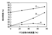
Example of changing ITO area and scattering intensity (Fig. 35)
Concavities and convexities are formed on the sides of the lower electrode, and openings and metal wires are formed on the lower electrode.
Example of formation (FIG. 36)
Example in which openings are formed in the lower electrode and the upper electrode (FIG. 37)
Examples of different positions of light modulation elements (FIGS. 38 to 40)
4). Examples and Comparative Examples (FIGS. 41 to 75)
5. Application example (Fig. 76)
Example in which the backlight of the above embodiment is applied as a light source of a display device
<1.第1の実施の形態>
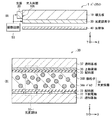
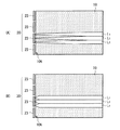
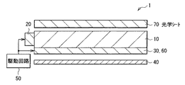
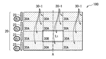
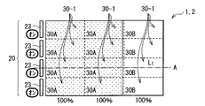
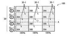
図1(A)は、本発明の第1の実施の形態に係るバックライト1(照明装置)の概略構成の一例を表す断面図である。図1(B)は、図1(A)のバックライト1に搭載された光変調素子30(後述)の構成の一例を表す断面図である。なお、図1(A),(B)は、模式的に表したものであり、実際の寸法や形状と同一であるとは限らない。バックライト1は、例えば、液晶表示パネルなどを背後から照明するものであり、導光板10と、導光板10の側面に配置した光源20と、導光板10の背後に配置した光変調素子30および反射板40と、光源20および光変調素子30を駆動する駆動回路50とを備えている。
<1. First Embodiment>
FIG. 1A is a cross-sectional view illustrating an example of a schematic configuration of the backlight 1 (illumination device) according to the first exemplary embodiment of the present invention. FIG. 1B is a cross-sectional view illustrating an example of a configuration of a light modulation element 30 (described later) mounted on the
光源20は、例えば、図2に示したように、複数の点状光源21を一列に配置して構成されたものである。各点状光源21は、導光板10の側面に向かって光を射出するようになっており、例えば、導光板10の側面との対向面に発光スポットを有する発光素子からなる。そのような発光素子としては、例えば、LED、または、レーザダイオード(LD;Laser Diode)などが挙げられる。効率、薄型化、均一性の観点からは、各点状光源21がホワイトLEDであることが好ましい。なお、光源20に含まれる複数の点状光源21が、例えば、赤色LED、緑色LEDおよび青色LEDを含んで構成されていてもよい。
For example, as illustrated in FIG. 2, the
複数の点状光源21は、例えば、図2に示したように、2個以上の点状光源21ごとに、共通の基板22上に設けられていてもよい。この場合、1つの基板22と、その基板22上に設けられた複数の点状光源21とにより、光源ブロック23が構成されている。基板22は、例えば、点状光源21と駆動回路50とを電気的に接続する配線が形成された回路基板であり、各点状光源21は、この回路基板上に実装されている。共通の基板22上に設けられた各点状光源21(光源ブロック23内の各点状光源21)は、駆動回路50によって一括で(非独立に)駆動されるようになっており、例えば、図示しないが、互いに並列に、または互いに直列に、接続されている。また、互いに異なる基板22上に設けられた点状光源21(各光源ブロック23内の点状光源21)は、駆動回路50によって互いに独立に駆動されるようになっており、例えば、図2に示したように、互いに異なる電流経路に接続されている。
For example, as shown in FIG. 2, the plurality of point
光源20は、図2に示したように、導光板10の1つの側面にだけ設けられていてもよいし、図示しないが、導光板10の2つの側面、3つの側面または全ての側面に設けられていてもよい。また、光源20が3つの側面または全ての側面に設けられている場合には、部分点灯を行うときにだけ、互いに対向する2つの側面に設けられた光源20だけを点灯させ、全面点灯を行うときに全ての光源20を点灯させるようにしてもよい。
As shown in FIG. 2, the
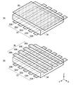
導光板10は、導光板10の1または複数の側面に配置した光源20からの光を導光板10の上面に導くものである。この導光板10は、導光板10の上面に配置される表示パネル(図示せず)に対応した形状、例えば、上面、下面および側面で囲まれた直方体状となっている。なお、以下では、導光板10の側面のうち光源20からの光が入射する側面を光入射面10Aと称するものとする。導光板10は、例えば、図3(A)に示したように、帯状の複数の凸部11を上面に有している。なお、導光板10は、例えば、図3(B)に示したように、帯状の複数の凸部11を下面に有していてもよい。また、導光板10は、例えば、図示しないが、導光板10の内部に設けられていてもよい。また、導光板10の内部が空洞状になっていてもよいし、密に充填されていてもよい。
The
各凸部11は、光入射面10Aの法線と平行な方向に延在しており、例えば、図3(A),(B)に示したように、導光板10の一の側面から、その側面と対向する他の側面まで連続して形成されている。各凸部11の配列方向の断面は、例えば、図4(A)〜(D)に示したように、矩形状、台形状、または三角形状となっている。各凸部11の配列方向の断面が矩形状となっている場合には、光の直進性が非常に高く、大型のバックライトに適している。各凸部11の配列方向の断面が台形状となっている場合には、射出成型、溶融押し出し成型、熱プレス成型などで各凸部11を形成する際に使用する金型の加工が容易であり、かつ成型時の離型性もよく、欠陥の減少による歩留まりや成型速度を向上させることができる。
Each
互いに隣り合う凸部11同士の間には、平坦面が設けられていてもよいし、平坦面がなくてもよい。各凸部11の高さは、面内で均一になっていてもよいし、面内で不均一になっていてもよい。例えば、図5に示したように、導光板10の1つの側面が光入射面10Aとなっているときに、各凸部11の高さが、光入射面10A側で相対的に低く、光入射面10Aと対向する側面側で相対的に高くなっていてもよい。また、例えば、導光板10の側面のうち互いに対向する一対の側面が光入射面10Aとなっているときに、各凸部11の高さが、双方の光入射面10Aおよびその近傍で相対的に低く、それ以外の部分で相対的に高くなっていてもよい。各凸部11のうち、光入射面10Aおよびその近傍の高さは、ゼロまたは実質的にゼロとなっていてもよい。例えば、図6に示したように、各凸部11の高さが、光入射面10A側から、光入射面10Aと対向する側面側に向かうにつれて高くなっていてもよい。このとき、各凸部11の高さが、光入射面10A側から、光入射面10Aと対向する側面側に向かう中途で、一定になるようになっていてもよい。なお、図5に示したような高さの不均一な複数の凸部11が導光板10の上面以外の箇所に設けられていてもよく、例えば、導光板10の下面または内部に設けられていてもよい。
A flat surface may be provided between the
上述のように、凸部11の高さ(言い換えると、凸部11同士の間に形成される溝の深さ)を変えることにより、光の直進性を変化させることができる。例えば、図3(A),(B)に示したように、各凸部11を光入射面10Aおよびその近傍にも設けた場合には、例えば、図7(A)に例示したように、1つの光源ブロック23を点灯させると、その光源ブロック23から出力された光L1は、横方向(幅方向)にあまり広がらずに導光板10内を伝播するようになる。この場合、光入射面10Aの近傍において、点状光源21同士の間に暗い部分が発生する場合があり、その場合には、画質が低下する虞がある。そのこで、そのような場合には、例えば、図5に示したように、各凸部11の高さを光入射面10Aおよびその近傍で相対的に低くしたり、またはゼロにしたりすることが好ましい。このようにすることにより、光源ブロック23から出力された光L1を、例えば、図7(B)に示したように、光入射面10Aおよびその近傍において、点状光源21の発散角で横方向(幅方向)に広げ、光入射面10Aから離れた領域においては、ほぼ一定の幅で伝播させることができる。
As described above, by changing the height of the protrusions 11 (in other words, the depth of the grooves formed between the protrusions 11), the straightness of light can be changed. For example, as shown in FIGS. 3A and 3B, when each
導光板10は、例えば、表示装置に適用された場合に、表示パネルとバックライト1との間に配置される光学シート(例えば、拡散板、拡散シート、レンズフィルム、偏光分離シートなど)を支持する支持体としても機能する。導光板10は、例えば、ポリカーボネート樹脂(PC)やアクリル樹脂(ポリメチルメタクリレート(PMMA)などの透明熱可塑性樹脂を主に含んで構成されている。
The
反射板40は、導光板10の背後から光変調素子30を介して漏れ出てきた光を導光板10側に戻すものであり、例えば、反射、拡散、散乱などの機能を有している。これにより、光源20からの射出光を効率的に利用することができ、また、正面輝度の向上にも役立っている。この反射板40は、例えば、発泡PET(ポリエチレンテレフタレート)や銀蒸着フィルム、多層膜反射フィルム、白色PETなどからなる。
The
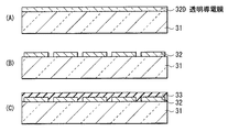
光変調素子30は、本実施の形態において、導光板10の背後(下面)に空気層を介さずに密着しており、例えば接着剤(図示せず)を介して導光板10の背後に接着されている。この光変調素子30は、例えば、図1(B)に示したように、透明基板31、下側電極32、配向膜33、光変調層34、配向膜35、上側電極36および透明基板37を反射板40側から順に配置したものである。
In the present embodiment, the
透明基板31,37は、光変調層34を支持するものであり、一般に、可視光に対して透明な基板、例えば、ガラス板や、プラスチックフィルムによって構成されている。下側電極32は、透明基板31のうち透明基板37との対向面上に設けられたものであり、例えば、図8(A),(B)に光変調素子30の一部を抜き出して示したように、面内の一の方向に延在する帯状の複数の部分電極32Aを互いに並列配置したものである。また、上側電極36は、透明基板37のうち透明基板31との対向面上に設けられたものであり、例えば、図8(A)に示したように、面内全体に渡って形成された単一のシート状の電極である。なお、上側電極36は、例えば、図8(B)に示したように、面内の一の方向であって、かつ下側電極32の延在方向と交差(または直交)する方向に延在する帯状の複数の部分電極36Aを互いに並列配置したものであってもよい。この場合に、各部分電極36Aが互いに電気的に接続されていてもよいし、互いに電気的に分離されていてもよい。
The
下側電極32および上側電極36のパターンは、駆動方式に依存するものである。例えば、下側電極32が複数の帯状の部分電極32Aを並列配置したものとなっており、かつ上側電極36が複数の帯状の部分電極36Aを並列配置したものとなっている場合には、例えば、各部分電極32A,36Aを単純マトリクス駆動することが可能である。上側電極36がベタ膜(表面全体に形成された膜)となっており、下側電極32が複数の帯状の部分電極32Aを並列配置したものとなっている場合には、例えば、各部分電極32Aを線順次駆動することが可能である。また、上側電極36がベタ膜(表面全体に形成された膜)となっており、下側電極32が複数の微小電極をマトリクス状に配置したものとなっている場合には、例えば、各微小電極をアクティブマトリクス駆動することが可能である。また、上側電極36がベタ膜となっており、下側電極32が細かな引出線がついた複数のブロック状電極からなる場合には、例えば、それぞれのブロック状電極を独自に駆動できるセグメント方式にすることもできる。
The pattern of the
下側電極32および上側電極36は、例えば、透明な導電性材料、例えば、酸化インジウムスズ(ITO;Indium Tin Oxide)からなる。透明な導電性材料は、可能な限り可視光の吸収が小さい材料であることが好ましい。光が導光板10内を導光する際に何度も光変調素子30の上側電極36および下側電極32を通過するので、大型のバックライト1では、光が面に垂直に入射した場合の可視光の吸収が数%であったとしても、画面中央部分での輝度が光入射面近傍での輝度と比べて数十%程度も減少してしまう場合がある。また、透明な導電性材料の吸収の波長依存性は小さい方が好ましい。特定の波長の吸収が大きい場合、光が導光板10内を導光するにつれて色度が変化してしまい、画面中央部と端部で色味が異なってしまう場合がある。
The
短波長領域の吸収を減少させるには、酸化インジウムスズなどの透明導電膜を結晶化させることが好ましい。アモルファス状態から結晶化させることによりバンドギャップが広がり、吸収領域が紫外へと移動して短波長領域の吸収が減少する。結晶化させる際には、透明基板31,37を加熱して透明導電膜を製膜したり、透明導電膜を製膜後にアニール処理したりするとよい。また、酸化インジウムスズの場合は格子欠陥生み出すスズの含有量を小さくすることがよい。ただし、スズの含有量が小さすぎると導電性を確保できないので、組成として酸化スズの含有量は3%から5%程度が好ましい。
In order to reduce absorption in the short wavelength region, it is preferable to crystallize a transparent conductive film such as indium tin oxide. By crystallizing from the amorphous state, the band gap widens, the absorption region moves to ultraviolet, and the absorption in the short wavelength region decreases. When crystallization is performed, the
ただし、下側電極32は、透明な材料でなくてもよく、例えば、金属によって構成されていてもよい。なお、下側電極32が金属によって構成されている場合には、下側電極32は、反射板40と同様、導光板10の背後から光変調素子30に入射する光を反射する機能も兼ね備えていることになる。従って、この場合には、例えば、図9に示したように、反射板40を省略することも可能である。
However, the
上側電極36がベタ膜(表面全体に形成された膜)となっている場合に、光変調素子30を光変調素子30の法線方向から見たときに、光変調素子30のうち部分電極32Aと対向する箇所が光変調セル30−1を構成している。例えば、図1(B)に破線で例示したような箇所が光変調セル30−1となっている。また、上側電極36が複数の部分電極36Aからなる場合に、光変調素子30を光変調素子30の法線方向から見たときに、光変調素子30のうち、部分電極32Aと部分電極36Aとの交差部分と対向する箇所が光変調セル30−1を構成している。各変調セル30−1は、下側電極32および上側電極36に所定の電圧を印加することにより別個独立に駆動することの可能なものであり、下側電極32および上側電極36に印加される電圧値の大きさに応じて、光源20からの光に対して透明性を示したり、散乱性を示したりする。なお、透明性、散乱性については、光変調層34を説明する際に詳細に説明する。
When the
配向膜33,35は、例えば、光変調層34に用いられる液晶やモノマーを配向させるものである。配向膜の種類としては、例えば、垂直用配向膜および水平用配向膜があるが、本実施の形態では、配向膜33,35には水平用配向膜が用いられる。水平用配向膜としては、例えば、ポリイミド、ポリアミドイミド、ポリビニルアルコールなどをラビング処理することにより形成された配向膜、転写やエッチングなどにより溝形状が付与された配向膜が挙げられる。また、水平用配向膜としては、例えば、酸化ケイ素などの無機材料を斜方蒸着することにより形成された配向膜、イオンビーム照射により形成されたダイヤモンドライクカーボン配向膜、電極パターンスリットの形成された配向膜が挙げられる。透明基板31,37としてプラスチックフィルムを用いる場合には、製造工程において、透明基板31,37の表面に配向膜33,35を塗布した後の焼成温度ができるだけ低いことが好ましいことから、配向膜33,35として、100℃以下の温度で形成可能なポリアミドイミドを用いることが好ましい。
For example, the
なお、水平用配向膜として、当該水平用配向膜に接する液晶分子にプレチルトを付与する機能を有するものが用いられてもよい。水平用配向膜にプレチルト機能を発現させる方法としては、例えば、ラビングなどが挙げられる。プレチルトとは、例えば、配向膜に近接する液晶分子の長軸が「配向膜の面内の特定の方向」または「配向膜の法線」と僅かな角度で交差することを意味している。上記の水平用配向膜は、例えば、当該水平用配向膜に近接する液晶分子の長軸を当該水平用配向膜の表面と平行な方向であって、かつ光入射面10Aの表面と僅かな角度で交差させる機能を有していてもよい。
As the horizontal alignment film, a film having a function of giving a pretilt to liquid crystal molecules in contact with the horizontal alignment film may be used. Examples of a method for causing the horizontal alignment film to exhibit a pretilt function include rubbing. The pretilt means, for example, that the major axis of the liquid crystal molecules adjacent to the alignment film intersects with “a specific direction in the plane of the alignment film” or “the normal of the alignment film” at a slight angle. The horizontal alignment film is, for example, a direction in which the major axis of the liquid crystal molecules adjacent to the horizontal alignment film is parallel to the surface of the horizontal alignment film and a slight angle with the surface of the
また、垂直、水平いずれの配向膜においても、液晶とモノマーを配向させる機能があれば十分であり、通常の液晶ディスプレイに要求される電圧の繰り返し印加による信頼性などは必要ない。デバイス作成後の電圧印加による信頼性は、モノマーを重合したものと液晶との界面で決まるためである。また、配向膜を用いなくても、例えば、下側電極32および上側電極36間に電場や磁場を印加することによっても、光変調層34に用いられる液晶やモノマーを配向させることが可能である。つまり、下側電極32および上側電極36間に電場や磁場を印加しながら、紫外線を照射して電圧印加状態での液晶やモノマーの配向状態を固定させることができる。配向膜の形成に電圧を用いる場合には、配向用と駆動用とで別々の電極を形成するか、液晶材料に周波数によって誘電率異方性の符号が反転する二周波液晶などを用いることができる。また、配向膜の形成に磁場を用いる場合、配向膜として磁化率異方性の大きい材料を用いることが好ましく、例えば、ベンゼン環の多い材料を用いることが好ましい。
Further, both the vertical and horizontal alignment films need only have a function of aligning the liquid crystal and the monomer, and do not require reliability due to repeated application of voltage required for a normal liquid crystal display. This is because the reliability due to the voltage application after device fabrication is determined by the interface between the polymerized monomer and the liquid crystal. Further, without using an alignment film, for example, by applying an electric field or a magnetic field between the
光変調層34は、電場の大きさに応じて、光源20からの光に対して散乱性もしくは透明性を示すものである。具体的には、光変調層34は、下側電極32および上側電極36に電圧が印加されていない時に光源20からの光に対して透明性を示し、下側電極32および上側電極36に電圧が印加されている時に光源20からの光に対して散乱性を示すものである。光変調層34は、例えば、図1(B)に示したように、バルク34Aと、バルク34A内に分散された微粒子状の複数の微粒子34Bとを含んだ複合層となっている。バルク34Aおよび微粒子34Bは光学異方性を有している。
The
図10は、下側電極32および上側電極36間に電圧が印加されていない時の、バルク34Aおよび微粒子34B内の配向状態の一例を模式的に表したものである。図10中の楕円体134Aは、下側電極32および上側電極36間に電圧が印加されていない時の、バルク34Aの屈折率異方性を示す屈折率楕円体の一例を表したものである。図10中の楕円体134Bは、下側電極32および上側電極36間に電圧が印加されていない時の、微粒子34Bの屈折率異方性を示す屈折率楕円体の一例を表したものである。この屈折率楕円体は、様々な方向から入射した直線偏光の屈折率をテンソル楕円体で表したものであり、光が入射する方向からの楕円体の断面を見ることによって、幾何的に屈折率を知ることができるものである。
FIG. 10 schematically shows an example of the orientation state in the bulk 34A and the fine particles 34B when no voltage is applied between the
図11は、下側電極32および上側電極36間に電圧が印加されている時の、バルク34Aおよび微粒子34B内の配向状態の一例を模式的に表したものである。図11中の楕円体134Aは、下側電極32および上側電極36間に電圧が印加されている時の、バルク34Aの屈折率異方性を示す屈折率楕円体の一例を表したものである。図11中の楕円体134Bは、下側電極32および上側電極36間に電圧が印加されている時の、微粒子34Bの屈折率異方性を示す屈折率楕円体の一例を表したものである。
FIG. 11 schematically shows an example of the orientation state in the bulk 34A and the fine particles 34B when a voltage is applied between the
バルク34Aおよび微粒子34Bは、例えば、図10に示したように、下側電極32および上側電極36間に電圧が印加されていない時に、バルク34Aの光軸AX1(楕円体134Aの長軸)および微粒子34Bの光軸AX2(楕円体134Bの長軸)の向きが互いに一致する(平行となる)構成となっている。なお、光軸AX1,AX2とは、偏光方向によらず屈折率が一つの値になるような光線の進行方向と平行な線を指している。また、下側電極32および上側電極36間に電圧が印加されていない時に、光軸AX1および光軸AX2の向きは常に互いに一致している必要はなく、光軸AX1の向きと光軸AX2の向きとが、例えば製造誤差などによって多少ずれていてもよい。
For example, as shown in FIG. 10, when the voltage is not applied between the
また、下側電極32および上側電極36間に電圧が印加されていない時に、光軸AX2は、導光板10の光入射面10Aと平行(またはほぼ平行)となると共に、透明基板31の表面と平行(またはほぼ平行)となっている。つまり、下側電極32および上側電極36間に電圧が印加されていない時に、光軸AX2は、下側電極32または上側電極36を含む面と平行(またはほぼ平行)となっており、かつ部分電極32Aの延在方向と平行(またはほぼ平行)となっている。
In addition, when no voltage is applied between the
一方、バルク34Aは、下側電極32および上側電極36間への電圧印加の有無に拘らず、光軸AX1が一定となる構成となっている。具体的には、光軸AX1は、導光板10の光入射面10Aと平行(またはほぼ平行)となると共に、透明基板31の表面と平行(またはほぼ平行)となっている。つまり、下側電極32および上側電極36間に電圧が印加されていない時に、光軸AX1は、光軸AX2と平行(またはほぼ平行)となっている。
On the other hand, the bulk 34A has a configuration in which the optical axis AX1 is constant regardless of the presence or absence of voltage application between the
なお、光軸AX2が常に、導光板10の光入射面10Aと平行となると共に透明基板31の表面と平行となっている必要はなく、例えば製造誤差などによって光入射面10Aおよび透明基板31の表面の少なくとも一方と小さな角度で交差する方向を向いていてもよい。
The optical axis AX2 is not always parallel to the
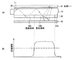
ここで、バルク34Aおよび微粒子34Bの常光屈折率が互いに等しく、かつバルク34Aおよび微粒子34Bの異常光屈折率が互いに等しいことが好ましい。この場合に、例えば、下側電極32および上側電極36間に電圧が印加されていない時には、正面方向および斜め方向を含むあらゆる方向において屈折率差がほとんどなく、高い透明性が得られる。これにより、例えば、正面方向に向かう光および斜め方向に向かう光は、光変調層34内で散乱されることなく、光変調層34を透過する。その結果、例えば、図12(A),(B)に示したように、光源20からの光L(斜め方向からの光)は、光変調素子30内で透明となった領域(透過領域30A)の界面(透明基板31または導光板10と空気との界面)において全反射され、透過領域30Aの輝度(黒表示の輝度)が、光変調素子30を設けていない場合(図12(B)中の一点鎖線)と比べて下がる。なお、図12(B)のグラフは、図12(A)に示したように導光板10の上に拡散シート41を配置した状態で、正面輝度を計測したときのものである。
Here, it is preferable that the ordinary light refractive indexes of the bulk 34A and the fine particles 34B are equal to each other, and the extraordinary refractive indexes of the bulk 34A and the fine particles 34B are equal to each other. In this case, for example, when no voltage is applied between the
また、バルク34Aおよび微粒子34Bは、例えば、下側電極32および上側電極36間に電圧が印加されている時には、図11に示したように、光軸AX1および光軸AX2の向きが互いに異なる(交差もしくは直交する)構成となっている。また、微粒子34Bは、例えば、下側電極32および上側電極36間に電圧が印加されている時に、光軸AX2が導光板10の光入射面10Aと平行(もしくはほぼ平行)となると共に透明基板31の法線と平行(もしくはほぼ平行)となる構成となっている。つまり、下側電極32および上側電極36間に電圧が印加されている時に、光軸AX2は、下側電極32または上側電極36を含む面と直交(もしくはほぼ直交)している。
Further, for example, when the voltage is applied between the
したがって、下側電極32および上側電極36間に電圧が印加されている時には、光変調層34において、光入射面10Aと平行な面内のあらゆる方向において屈折率差が大きくなり、高い散乱性が得られる。これにより、例えば、正面方向に向かう光および斜め方向に向かう光は、光変調層34内で散乱される。その結果、例えば、図12(A),(B)に示したように、光源20からの光L(斜め方向からの光)は、光変調素子30内で散乱状態となった領域(散乱領域30B)の界面(透明基板31または導光板10と空気との界面)を透過すると共に、反射板40側に透過した光は反射板40で反射され、光変調素子30を透過する。従って、散乱領域30Bの輝度は、光変調素子30を設けていない場合(図12(B)中の一点鎖線)と比べて極めて高くなり、しかも、透過領域30Aの輝度が低下した分だけ、部分的な白表示の輝度(輝度突き上げ)が大きくなる。
Therefore, when a voltage is applied between the
なお、バルク34Aおよび微粒子34Bの常光屈折率は、例えば製造誤差などによって多少ずれていてもよく、例えば、0.1以下であることが好ましく、0.05以下であることがより好ましい。また、バルク34Aおよび微粒子34Bの異常光屈折率についても、例えば製造誤差などによって多少ずれていてもよく、例えば、0.1以下であることが好ましく、0.05以下であることがより好ましい。 Note that the ordinary refractive indexes of the bulk 34A and the fine particles 34B may be slightly deviated due to, for example, manufacturing errors, and are preferably 0.1 or less, and more preferably 0.05 or less. Further, the extraordinary light refractive indexes of the bulk 34A and the fine particles 34B may be slightly deviated due to, for example, manufacturing errors, and are preferably 0.1 or less, and more preferably 0.05 or less.
また、バルク34Aの屈折率差(=異常光屈折率−常光屈折率)や、微粒子34Bの屈折率差(=異常光屈折率−常光屈折率)は、できるだけ大きいことが好ましく、0.05以上であることが好ましく、0.1以上であることがより好ましく、0.15以上であることがさらに好ましい。バルク34Aおよび微粒子34Bの屈折率差が大きい場合には、光変調層34の散乱能が高くなり、導光条件を容易に破壊することができ、導光板10からの光を取り出しやすいからである。
Further, the refractive index difference (= extraordinary refractive index−ordinary refractive index) of the bulk 34A and the refractive index difference (= extraordinary refractive index—ordinary refractive index) of the fine particles 34B are preferably as large as possible, and are 0.05 or more. Is preferably 0.1 or more, more preferably 0.15 or more. This is because, when the difference in refractive index between the bulk 34A and the fine particles 34B is large, the
また、バルク34Aおよび微粒子34Bは、電場に対する応答速度が互いに異なっている。バルク34Aは、例えば、電場に対して応答しない筋状構造もしくは多孔質構造となっているか、または微粒子34Bの応答速度よりも遅い応答速度を有する棒状構造となっている。バルク34Aは、例えば、低分子モノマーを重合化することにより得られた高分子材料によって形成されている。バルク34Aは、例えば、微粒子34Bの配向方向または配向膜33,35の配向方向に沿って配向した、配向性および重合性を有する材料(例えばモノマー)を熱および光の少なくとも一方によって重合させることにより形成されている。
Further, the bulk 34A and the fine particles 34B have different response speeds with respect to the electric field. The bulk 34A has, for example, a streak structure or a porous structure that does not respond to an electric field, or a rod-like structure having a response speed slower than that of the fine particles 34B. The bulk 34A is formed of, for example, a polymer material obtained by polymerizing a low molecular weight monomer. For example, the bulk 34A is obtained by polymerizing a material having alignment properties and polymerizability (for example, a monomer) aligned along the alignment direction of the fine particles 34B or the alignment direction of the
一方、微粒子34Bは、例えば、液晶材料を主に含んで構成されており、バルク34Aの応答速度よりも十分に早い応答速度を有している。微粒子34B内に含まれる液晶材料(液晶分子)は、例えば棒状分子である。微粒子34B内に含まれる液晶分子として、正の誘電率異方性を有するもの(いわゆるポジ型液晶)を用いることが好ましい。 On the other hand, the fine particles 34B are mainly composed of, for example, a liquid crystal material, and have a response speed sufficiently faster than the response speed of the bulk 34A. The liquid crystal material (liquid crystal molecules) contained in the fine particles 34B is, for example, a rod-like molecule. As the liquid crystal molecules contained in the fine particles 34B, those having positive dielectric anisotropy (so-called positive liquid crystal) are preferably used.
ここで、下側電極32および上側電極36間に電圧が印加されていない時には、微粒子34B内において、液晶分子の長軸方向は、光軸AX1と平行となっている。このとき、微粒子34B内の液晶分子の長軸は、導光板10の光入射面10Aと平行(もしくはほぼ平行)となると共に透明基板31の表面と平行(もしくはほぼ平行)となっている。また、下側電極32および上側電極36間に電圧が印加されている時には、微粒子34B内において、液晶分子の長軸方向は、光軸AX1と交差(もしくは直交)している。このとき、微粒子34B内の液晶分子の長軸は、導光板10の光入射面10Aと平行(もしくはほぼ平行)となると共に透明基板31の法線と平行(もしくはほぼ平行)となっている。
Here, when no voltage is applied between the
上記した、配向性および重合性を有するモノマーとしては、光学的に異方性を有しており、かつ液晶と複合する材料であればよいが、本実施の形態では紫外線で硬化する低分子モノマーであることが好ましい。電圧無印加の状態で、液晶と、低分子モノマーを重合化することにより形成されたもの(高分子材料)との光学的異方性の方向が一致していることが好ましいので、紫外線硬化前において、液晶と低分子モノマーが同一方向に配向していることが好ましい。微粒子34Bとして液晶が用いられる場合に、その液晶が棒状分子であるときには、使用するモノマー材料の形状も棒状であることが好ましい。以上のことから、モノマー材料としては重合性と液晶性を併せ持つ材料を用いることが好ましく、例えば、重合性官能基として、アクリレート基、メタクリレート基、アクリロイルオキシ基、メタクリロイルオキシ基、ビニルエーテル基およびエポキシ基からなる群から選ばれた少なくとも1つの官能基を有することが好ましい。これらの官能基は、紫外線、赤外線または電子線を照射したり、加熱したりすることによって重合させることができる。紫外線照射時の配向度低下を抑制するために、多官能基をもつ液晶性材料を添加することもできる。バルク34Aを上述した筋状構造とする場合には、バルク34Aの原料として、2官能液晶性モノマーを用いることが好ましい。また、バルク34Aの原料に対して、液晶性を示す温度の調整を目的に単官能モノマーを添加したり、架橋密度向上を目的に3官能以上のモノマーを添加したりすることもできる。 As the above-mentioned monomer having orientation and polymerizability, any material that has optical anisotropy and is composited with liquid crystal may be used. In this embodiment, a low molecular weight monomer that cures with ultraviolet rays. It is preferable that It is preferable that the direction of optical anisotropy between the liquid crystal and the one formed by polymerizing a low molecular weight monomer (polymer material) in the state where no voltage is applied is the same before UV curing. The liquid crystal and the low molecular weight monomer are preferably aligned in the same direction. When liquid crystal is used as the fine particles 34B, when the liquid crystal is a rod-like molecule, it is preferable that the monomer material used has a rod-like shape. From the above, it is preferable to use a material having both polymerizability and liquid crystallinity as the monomer material. For example, as a polymerizable functional group, an acrylate group, a methacrylate group, an acryloyloxy group, a methacryloyloxy group, a vinyl ether group, and an epoxy group. It preferably has at least one functional group selected from the group consisting of These functional groups can be polymerized by irradiation with ultraviolet rays, infrared rays or electron beams, or by heating. A liquid crystalline material having a polyfunctional group can also be added in order to suppress a decrease in the degree of alignment during ultraviolet irradiation. When the bulk 34A has the above-described streak structure, it is preferable to use a bifunctional liquid crystalline monomer as a raw material for the bulk 34A. In addition, a monofunctional monomer may be added to the raw material of the bulk 34A for the purpose of adjusting the temperature exhibiting liquid crystallinity, or a trifunctional or higher functional monomer may be added for the purpose of improving the crosslinking density.
駆動回路50は、例えば、ある光変調セル30−1において微粒子34Bの光軸AX2がバルク34Aの光軸AX1と平行もしくはほぼ平行となり、他の光変調セル30−1において微粒子34Bの光軸AX2がバルク34Aの光軸AX1と交差もしくは直交するように部分電極32Aへ印加する電圧の大きさを制御するようになっている。つまり、駆動回路50は、電場制御によって、バルク34Aおよび微粒子34Bの光軸AX1,AX2の向きを互いに一致(もしくはほぼ一致)させたり、互いに異ならせたり(もしくは直交させたり)することができるようになっている。
For example, in the light modulation cell 30-1, the
また、駆動回路50は、例えば、部分電極32Aの光源20からの距離に応じて、波高値、デューティ比および周波数が変調された電圧を部分電極32Aに印加するようになっている。電圧の変調は、例えば、光源20からの距離が遠くなるにつれて光変調セル30−1の散乱性が強まるようになされる。さらに、駆動回路50は、例えば、部分電極32Aの光源20からの距離だけでなく、外部から入力される映像信号も考慮して、波高値、デューティ比および周波数が変調された電圧を部分電極32Aに印加するようになっていてもよい。
In addition, the
また、駆動回路50は、例えば、電圧印加対象の部分電極32Aの光源20からの距離と、外部から入力される映像信号とに応じて、波高値、デューティ比および周波数が変調された電力を各光源ブロック23に印加するようになっていてもよい。また、駆動回路50は、例えば、各光源ブロック23に順次、電力を供給することにより、各光源ブロック23をスキャンするようになっていてもよい。
In addition, the
以下に、本実施の形態のバックライト1の製造方法について、図13(A)〜(C)から図15(A)〜(C)を参照しながら説明する。
Below, the manufacturing method of the
まず、ガラス基板またはプラスチックフィルム基板からなる透明基板31上に、ITOなどの透明導電膜32Dを形成する(図13(A))。次に、透明導電膜32D上に、パターニングされたレジスト層(図示せず)を形成したのち、レジスト層をマスクとして透明導電膜32Dを選択的にエッチングする。その結果、下側電極32が形成される(図13(B))。
First, a transparent conductive film 32D such as ITO is formed on a
次に、表面全体に配向膜33を塗布したのち、乾燥させ、焼成する(図13(C))。配向膜33としてポリイミド系材料を用いる場合には、溶媒にNMP(N−メチル−2−ピロリドン)を用いることが多いが、そのときには、大気下では200℃程度の温度が必要である。なお、この場合に、透明基板31,37としてプラスチック基板を用いる場合には、配向膜33を100℃で真空乾燥させ、焼成することもできる。その後、配向膜33に対してラビング処理を行う。これにより、配向膜33が水平配向用の配向膜として機能することが可能となる。
Next, after the
次に、配向膜33上に、セルギャップを形成するためのスペーサ38を乾式または湿式で散布する(図14(A))。なお、真空貼り合わせ法にて光変調セル30−1を作成する場合には、滴下する混合物中にスペーサ38を混合しておいてもよい。また、スペーサ38の替わりとして、フォトリソ法によって柱スペーサを形成することもできる。
Next,
続いて、上記と同様の方法で作製しておいた配向膜35上に、貼り合わせおよび液晶の漏れを防止するためのシール剤39を、例えば額縁状に塗布する(図14(B))。このシール剤パターン39はディスペンサー法やスクリーン印刷法にて形成することができる。
Subsequently, a sealing
以下に、真空貼り合わせ法(One Drop Fill法、ODF法)について説明するが、真空注入法やロール貼合方式などで光変調セル30−1を作成することも可能である。 Although the vacuum bonding method (One Drop Fill method, ODF method) is demonstrated below, it is also possible to create the light modulation cell 30-1 by a vacuum injection method, a roll bonding method, etc.
まず、セルギャップ、セル面積などから決まる体積分にあたる液晶とモノマーの混合物42を面内に均一に滴下する(図14(C))。混合物42の滴下にはリニアガイド方式の精密ディスペンサーを用いることが好ましいが、シール剤パターン39を土手として利用して、ダイコータなどを用いてもよい。
First, a liquid crystal and
液晶とモノマーは前述の材料を用いることができるが、液晶とモノマーの重量比は98:2〜50:50、好ましくは95:5〜75:25、より好ましくは92:8〜85:15である。液晶の比率を多くすることで駆動電圧を低くすることができるが、あまり液晶を多くしすぎると電圧印加時の白色度が低下したり、電圧オフ後に応答速度が低下するなど透明時に戻りにくくなったりする傾向がある。 The above-mentioned materials can be used for the liquid crystal and the monomer, but the weight ratio of the liquid crystal to the monomer is 98: 2 to 50:50, preferably 95: 5 to 75:25, more preferably 92: 8 to 85:15. is there. The drive voltage can be lowered by increasing the ratio of the liquid crystal, but if too much liquid crystal is added too much, the whiteness at the time of voltage application will decrease or the response speed will decrease after the voltage is turned off, making it difficult to return to transparency. There is a tendency to.
混合物42には、液晶とモノマーの他には、重合開始剤を添加する。使用する紫外線波長に応じて、添加する重合開始剤のモノマー比を0.1〜10重量%の範囲内で調整する。混合物42には、この他に、重合禁止剤や可塑剤、粘度調整剤なども必要に応じて添加可能である。モノマーが室温で固体やゲル状である場合には、口金やシリンジ、基板を加温することが好ましい。
In addition to the liquid crystal and the monomer, a polymerization initiator is added to the
透明基板31および透明基板36を真空貼り合わせ機(図示せず)に配置したのち、真空排気し、貼り合わせを行う(図15(A))。その後、貼り合わせたものを大気に解放し、大気圧での均一加圧によってセルギャップを均一化する。セルギャップは白輝度(白色度)と駆動電圧の関係から適宜選定できるが、5〜40μm、好ましくは6〜20μm、より好ましくは7〜10μmである。
After the
貼り合わせ後、必要に応じて配向処理を行うことが好ましい(図示せず)。クロスニコル偏光子の間に、貼り合わせたセルを挿入した際に、光り漏れが生じている場合には、セルをある一定時間加熱処理したり、室温で放置したりして配向させる。その後、紫外線L3を照射してモノマーを重合させてポリマー化する(図15(B))。このようにして、光変調素子30が製造される。
After bonding, it is preferable to perform an alignment treatment as necessary (not shown). When light leakage occurs when a bonded cell is inserted between crossed Nicol polarizers, the cell is oriented by being heat-treated for a certain period of time or left at room temperature. Thereafter, the monomer is polymerized by irradiating with ultraviolet rays L3 to form a polymer (FIG. 15B). In this way, the
紫外線を照射している時には、セルの温度が変化しないようにすることが好ましい。赤外線カットフィルターを用いたり、光源にUV−LEDなどを用いたりすることが好ましい。紫外線照度は複合材料の組織構造に影響を与えるので、使用する液晶材料やモノマー材料、これらの組成から適宜調整することが好ましく、0.1〜500mW/cm2の範囲が好ましく、さらに好ましくは0.5〜30mW/cm2である。紫外線照度が低いほど駆動電圧が低くなる傾向にあり、生産性と特性の両面から好ましい紫外線照度を選定することができる。 It is preferable that the temperature of the cell does not change during irradiation with ultraviolet rays. It is preferable to use an infrared cut filter or a UV-LED as a light source. Since the ultraviolet illuminance affects the structure of the composite material, it is preferably adjusted as appropriate from the liquid crystal material and monomer material used, and their composition, preferably in the range of 0.1 to 500 mW / cm 2 , more preferably 0. 5 to 30 mW / cm 2 . The driving voltage tends to be lower as the ultraviolet illuminance is lower, and a preferable ultraviolet illuminance can be selected from both aspects of productivity and characteristics.
そして、導光板10に光変調素子30を貼り合わせる(図15(C))。貼り合わせには、粘着、接着のいずれでもよいが、導光板10の屈折率と光変調素子30の基板材料の屈折率とにできるだけ近い屈折率の材料で粘着、接着することが好ましい。最後に、下側電極32および上側電極36に引き出し線(図示せず)を取り付ける。このようにして、本実施の形態のバックライト1が製造される。
Then, the
このように、光変調素子30を作成し、最後に導光板10に光変調素子30を貼り合わせるプロセスを説明したが、導光板10の表面に、配向膜35を形成した透明基板36を予め貼り合わせてから、バックライト1を作成することもできる。また、枚葉方式、ロール・ツー・ロール方式のいずれでもバックライト1を作成することができる。
As described above, the process of creating the
次に、本実施の形態のバックライト1の作用および効果について説明する。
Next, the operation and effect of the
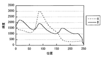
本実施の形態のバックライト1では、例えば、光変調セル30−1において微粒子34Bの光軸AX2がバルク34Aの光軸AX1と平行もしくはほぼ平行となり、別の光変調セル30Bにおいて微粒子34Bの光軸AX2がバルク34Aの光軸AX1と交差もしくは直交するように、各光変調セル30Bの下側電極32および上側電極36間に電圧が印加される。これにより、光源20から射出され、導光板10内に入射した光は、光変調素子30のうち、光軸AX1と光軸AX2とが互いに平行もしくはほぼ平行となっている透過領域30Aを透過する。一方、光源20から射出され、導光板10内に入射した光は、光変調素子30のうち、光軸AX1と光軸AX2とが互いに交差もしくは直交している散乱領域30Bにおいて散乱される。この散乱光のうち散乱領域30Bの下面を透過した光は反射板40で反射され、再度、導光板10に戻されたのち、バックライト1の上面から射出される。また、散乱光のうち、散乱領域30Bの上面に向かった光は、導光板10を透過したのち、バックライト1の上面から射出される。このように、本実施の形態では、透過領域30Aの上面からは光はほとんど射出されず、散乱領域30Bの上面から光が射出される。このようにして、正面方向の変調比を大きくしている。
In the
一般に、PDLCは、液晶材料と等方性の低分子材料とを混合し、紫外線照射や溶媒の乾燥などにより相分離を起こさせることによって形成され、液晶材料の微小粒子が高分子材料中に分散された複合層となっている。この複合層中の液晶材料は、電圧無印加時にはランダムな方向を向いているので散乱性を示すが、電圧印加時には電場方向に配向するので、液晶材料の常光屈折率と高分子材料の屈折率とが互いに等しい場合には、正面方向(PDLCの法線方向)において高い透明性を示す。しかし、この液晶材料では、斜め方向においては、液晶材料の異常光屈折率と高分子材料との差が顕著となり、正面方向が透明性であっても斜め方向において散乱性が発現してしまう。 In general, PDLC is formed by mixing liquid crystal material and isotropic low molecular weight material and causing phase separation by ultraviolet irradiation or solvent drying, and the fine particles of liquid crystal material are dispersed in the polymer material. It is a composite layer. The liquid crystal material in this composite layer is scattered in a random direction when no voltage is applied, but is oriented in the direction of the electric field when a voltage is applied, so the normal refractive index of the liquid crystal material and the refractive index of the polymer material Are equal to each other, high transparency is exhibited in the front direction (normal direction of PDLC). However, in this liquid crystal material, the difference between the extraordinary refractive index of the liquid crystal material and the polymer material becomes noticeable in the oblique direction, and the scattering property appears in the oblique direction even if the front direction is transparent.
通常、PDLCを使った光変調素子は、表面に透明導電膜の形成された2枚のガラス板の間にPDLCを挟み込んだ構造となっていることが多い。上述したような構造を有する光変調素子に対して空気中から斜めに光が入射した場合には、その斜め方向から入射した光は空気とガラス板の屈折率差によって屈折し、より小さな角度でPDLCに入射することになる。そのため、このような光変調素子においては、大きな散乱は生じない。例えば、空気中から80°の角度で光が入射した場合には、その光のPDLCへの入射角はガラス界面での屈折によって40°程度にまで小さくなる。 Usually, a light modulation element using PDLC often has a structure in which PDLC is sandwiched between two glass plates having a transparent conductive film formed on the surface thereof. When light is incident obliquely from the air on the light modulation element having the structure as described above, the light incident from the oblique direction is refracted by the difference in refractive index between the air and the glass plate, and at a smaller angle. The light enters the PDLC. Therefore, no large scattering occurs in such a light modulation element. For example, when light is incident from the air at an angle of 80 °, the incident angle of the light on the PDLC is reduced to about 40 ° due to refraction at the glass interface.
しかし、導光板を用いたエッジライト方式では、導光板越しに光が入射するので、光が80°程度の大きな角度でPDLC中を横切ることになる。そのため、液晶材料の異常光屈折率と高分子材料の屈折率との差が大きく、さらに、より大きな角度で光がPDLC中を横切るので、散乱を受ける光路も長くなる。例えば、常光屈折率1.5、異常光屈折率1.65の液晶材料の微小粒子が屈折率1.5の高分子材料中に分散されている場合には、正面方向(PDLCの法線方向)においては屈折率差がないが、斜め方向においては屈折率差が大きくなる。このため、斜め方向の散乱性を小さくすることができないので、視野角特性が悪い。さらに、導光板上に拡散フィルムなどの光学フィルムを設けた場合には、斜め漏れ光が拡散フィルムなどによって正面方向にも拡散されるので、正面方向の光漏れが大きくなり、正面方向の変調比が低くなってしまう。 However, in the edge light system using the light guide plate, light enters through the light guide plate, so that light crosses the PDLC at a large angle of about 80 °. For this reason, the difference between the extraordinary refractive index of the liquid crystal material and the refractive index of the polymer material is large, and furthermore, since the light crosses the PDLC at a larger angle, the optical path that receives the scattering becomes longer. For example, when fine particles of a liquid crystal material having an ordinary light refractive index of 1.5 and an extraordinary light refractive index of 1.65 are dispersed in a polymer material having a refractive index of 1.5, the front direction (the normal direction of the PDLC) ), There is no difference in refractive index, but the difference in refractive index increases in the oblique direction. For this reason, since the scattering property in the oblique direction cannot be reduced, the viewing angle characteristics are poor. In addition, when an optical film such as a diffusion film is provided on the light guide plate, oblique leakage light is also diffused in the front direction by the diffusion film, etc., so that light leakage in the front direction increases, and the modulation ratio in the front direction is increased. Will be lower.
一方、本実施の形態では、バルク34Aおよび微粒子34Bが光学異方性材料を主に含んで形成されているので、斜め方向において、散乱性が小さくなり、透明性を向上させることができる。例えば、バルク34Aおよび微粒子34Bが、互いに常光屈折率が等しく、かつ互いに異常光屈折率も等しい光学異方性材料を主に含んで構成され、かつ、下側電極32および上側電極36間に電圧が印加されていない領域では、これらの光軸の向きが一致もしくはほぼ一致する。これにより、正面方向(光変調素子30の法線方向)および斜め方向を含むあらゆる方向において屈折率差が少なくなるか、またはなくなり、高い透明性が得られる。その結果、視野角の大きい範囲における光の漏洩を低減またはほとんどなくすることができ、視野角特性を良くすることができる。
On the other hand, in the present embodiment, since the bulk 34A and the fine particles 34B are mainly formed of an optically anisotropic material, the scattering property is reduced in the oblique direction, and the transparency can be improved. For example, the
例えば、常光屈折率1.5、異常光屈折率1.65の液晶と、常光屈折率1.5、異常光屈折率1.65の液晶性モノマーとを混合し、配向膜または電界によって液晶と液晶性モノマーを配向させた状態で液晶性モノマーを重合させると、液晶の光軸と、液晶性モノマーが重合することによって形成されたポリマーの光軸とが互いに一致する。これにより、あらゆる方向で屈折率を一致させることができるので、そのようにした場合には、透明性が高い状態を実現でき、より一層、視野角特性を良くすることができる。 For example, a liquid crystal having an ordinary light refractive index of 1.5 and an extraordinary light refractive index of 1.65 is mixed with a liquid crystalline monomer having an ordinary light refractive index of 1.5 and an extraordinary light refractive index of 1.65, and the liquid crystal is formed by an alignment film or an electric field. When the liquid crystalline monomer is polymerized in a state where the liquid crystalline monomer is aligned, the optical axis of the liquid crystal and the optical axis of the polymer formed by polymerizing the liquid crystalline monomer coincide with each other. Thereby, since the refractive index can be matched in all directions, in such a case, a highly transparent state can be realized, and the viewing angle characteristics can be further improved.
また、本実施の形態では、例えば、図12(A),(B)に示したように、透過領域30Aの輝度(黒表示の輝度)が、光変調素子30を設けていない場合(図12(B)中の一点鎖線)と比べて下がっている。他方、散乱領域30Bの輝度は、光変調素子30を設けていない場合(図12(B)中の一点鎖線)と比べて極めて高くなり、しかも、透過領域30Aの輝度が低下した分だけ、部分的な白表示の輝度(輝度突き上げ)が大きくなる。
In the present embodiment, for example, as shown in FIGS. 12A and 12B, the luminance of the
ところで、輝度突き上げとは、全面白表示した場合に比べて、部分的に白表示を行った場合の輝度を高くする技術である。CRTやPDPなどでは一般によく使われている技術である。しかし、液晶ディスプレイでは、バックライトは画像にかかわらず全体に均一発光しているので、部分的に輝度を高くすることはできない。もっとも、バックライトを、複数のLEDを2次元配置したLEDバックライトとした場合には、LEDを部分的に消灯することは可能である。しかし、そのようにした場合には、LEDを消灯した暗領域からの拡散光がなくなるので、全てのLEDを点灯した場合と比べて、輝度が低くなってしまう。また、部分的に点灯しているLEDに対して流す電流を大きくすることにより、輝度を増やすことも可能であるが、そのようにした場合には、非常に短時間に大電流が流れるので、回路の負荷や信頼性の点で問題が残る。 By the way, the luminance increase is a technique for increasing the luminance when the white display is partially performed as compared with the case where the entire white display is performed. This technique is commonly used in CRT and PDP. However, in the liquid crystal display, the backlight emits light uniformly regardless of the image, and thus the brightness cannot be partially increased. However, if the backlight is an LED backlight in which a plurality of LEDs are two-dimensionally arranged, the LEDs can be partially turned off. However, in such a case, since there is no diffused light from the dark area where the LEDs are turned off, the luminance is lower than when all the LEDs are turned on. In addition, it is possible to increase the luminance by increasing the current flowing to the partially lit LED, but in such a case, a large current flows in a very short time, Problems remain in terms of circuit load and reliability.
一方、本実施の形態では、バルク34Aおよび微粒子34Bが光学異方性材料を主に含んで形成されているので、斜め方向の散乱性が抑制され、暗状態での導光板からの漏れ光が少ない。これにより、部分的な暗状態の部分から部分的な明状態の部分に導光するので、バックライト1への投入電力を増やすことなく、輝度突き上げを実現することができる。
On the other hand, in the present embodiment, since the bulk 34A and the fine particles 34B are mainly formed by including an optically anisotropic material, scattering in an oblique direction is suppressed, and light leaked from the light guide plate in a dark state is prevented. Few. As a result, light is guided from a partial dark state portion to a partial bright state portion, so that it is possible to increase the luminance without increasing the input power to the
また、本実施の形態では、導光板10に複数の帯状の凸部11が設けられており、凸部11と交差する方向に延在する複数の部分電極32Aが設けられている。さらに、本実施の形態では、光源20が、互いに独立駆動可能な複数の光源ブロック23からなる。これにより、例えば、1つの光源ブロック23を点灯させると共に、1つの部分電極32Aを駆動させることにより、点灯した光源ブロック23から出力された光は導光板10内を凸部11に沿って伝播し、さらに、導光板10の法線方向から見たときに、導光板10内を凸部11に沿って光が伝播する部分と、駆動された部分電極32Aとが互いに交わる部分(以下、「交差部分」と称する。)から光が取り出される。このとき、光変調層34のうち、駆動された部分電極32Aに対応する部分が散乱性を示しており、交差部分のうち部分電極32Aの延在方向に対向する1対の辺部には、光変調層34内に形成される散乱性と透明性との境界線が存在しない。従って、導光板10から取り出された光の輝度分布は、部分電極32Aの延在方向において緩やかに変化する。以上のことから、本実施の形態では、薄型化を阻害することなく、照明光における明暗の境界部分をぼかすことができる。また、本実施の形態では、各光源ブロック23を順次点灯させると共に、1または複数の部分電極32Aを駆動させることにより、単純マトリクス駆動を実現することができる。
In the present embodiment, the
<2.第2の実施の形態>
図16(A)は、本発明の第2の実施の形態に係るバックライト2(照明装置)の概略構成の一例を表す断面図である。図16(B)は、図16(A)のバックライト2の詳細な構成の一例を表す断面図である。なお、図16(A),(B)は、模式的に表したものであり、実際の寸法や形状と同一であるとは限らない。
<2. Second Embodiment>
FIG. 16A is a cross-sectional view illustrating an example of a schematic configuration of the backlight 2 (illumination device) according to the second exemplary embodiment of the present invention. FIG. 16B is a cross-sectional view illustrating an example of a detailed configuration of the
本実施の形態のバックライト2は、光変調素子30の代わりに光変調素子60を備えている点で、上記第1の実施の形態およびその変形例に係るバックライト1の構成と相違する。そこで、以下では、上記実施の形態との相違点について主に説明し、上記実施の形態との共通点についての説明を適宜省略するものとする。
The
光変調素子60は、本実施の形態において、導光板10の背後(下面)に空気層を介さずに密着しており、例えば接着剤(図示せず)を介して導光板10の背後に接着されている。この光変調素子60は、例えば、図16(B)に示したように、透明基板31、下側電極32、配向膜63、光変調層64、配向膜65、上側電極36および透明基板37を反射板40側から順に配置したものである。
In the present embodiment, the
配向膜63,65は、例えば、光変調層64に用いられる液晶やモノマーを配向させるものである。配向膜の種類としては、例えば、垂直用配向膜および水平用配向膜があるが、本実施の形態では、配向膜63,65には垂直用配向膜が用いられる。垂直用配向膜としては、シランカップリング材料や、ポリビニルアルコール(PVA)、ポリイミド系材料、界面活性剤などを用いることが可能である。また、透明基板31,37としてプラスチックフィルムを用いる場合には、製造工程において、透明基板31,37の表面に配向膜63,65を塗布した後の焼成温度ができるだけ低いことが好ましいことから、配向膜63,65としてアルコール系溶媒を使用することの可能なシランカップリング材料を用いることが好ましい。
For example, the
なお、垂直用配向膜として、当該垂直用配向膜に接する液晶分子にプレチルトを付与する機能を有するものが用いられてもよい。垂直用配向膜にプレチルト機能を発現させる方法としては、例えば、ラビングなどが挙げられる。上記の垂直用配向膜は、例えば、当該垂直用配向膜に近接する液晶分子の長軸を当該垂直用配向膜の法線と僅かな角度で交差させる機能を有していてもよい。 As the vertical alignment film, a film having a function of imparting a pretilt to liquid crystal molecules in contact with the vertical alignment film may be used. Examples of the method for causing the vertical alignment film to exhibit the pretilt function include rubbing. For example, the vertical alignment film may have a function of causing the major axis of the liquid crystal molecules adjacent to the vertical alignment film to intersect the normal line of the vertical alignment film at a slight angle.
ただし、配向膜63,65として垂直用配向膜を用いるに際しては、後述の微粒子64B内に含まれる液晶分子として、負の誘電率異方性を有するもの(いわゆるネガ型液晶)を用いることが好ましい。
However, when a vertical alignment film is used as the
次に、本実施の形態の光変調層64について説明する。光変調層64は、例えば、図16(B)に示したように、バルク64Aと、バルク64A内に分散された微粒子状の複数の微粒子64Bとを含んだ複合層となっている。バルク64Aおよび微粒子64Bは光学異方性を有している。
Next, the
図17は、下側電極32および上側電極36間に電圧が印加されていない時の、バルク64Aおよび微粒子64B内の配向状態の一例を模式的に表したものである。図17中の楕円体164Aは、下側電極32および上側電極36間に電圧が印加されていない時の、バルク64Aの屈折率異方性を示す屈折率楕円体の一例を表したものである。図17中の楕円体164Bは、下側電極32および上側電極36間に電圧が印加されていない時の、微粒子64Bの屈折率異方性を示す屈折率楕円体の一例を表したものである。
FIG. 17 schematically shows an example of the orientation state in the bulk 64A and the
図18は、下側電極32および上側電極36間に電圧が印加されている時の、バルク64Aおよび微粒子64B内の配向状態の一例を模式的に表したものである。図18中の楕円体164Aは、下側電極32および上側電極36間に電圧が印加されている時の、バルク64Aの屈折率異方性を示す屈折率楕円体の一例を表したものである。図18中の楕円体164Bは、下側電極32および上側電極36間に電圧が印加されている時の、微粒子64Bの屈折率異方性を示す屈折率楕円体の一例を表したものである。
FIG. 18 schematically shows an example of the orientation state in the bulk 64A and the
バルク64Aおよび微粒子64Bは、例えば、図17に示したように、下側電極32および上側電極36間に電圧が印加されていない時に、バルク64Aの光軸AX3(楕円体164Aの長軸)および微粒子64Bの光軸AX4(楕円体164Bの長軸)の向きが互いに一致する(平行となる)構成となっている。なお、光軸AX3,AX4とは、偏光方向によらず屈折率が一つの値になるような光線の進行方向と平行な線を指している。また、下側電極32および上側電極36間に電圧が印加されていない時に、光軸AX3および光軸AX4の向きは常に互いに一致している必要はなく、光軸AX3の向きと光軸AX4の向きとが、例えば製造誤差などによって多少ずれていてもよい。
For example, as shown in FIG. 17, when the voltage is not applied between the
また、下側電極32および上側電極36間に電圧が印加されていない時に、光軸AX4は、導光板10の光入射面10Aと平行(またはほぼ平行)となると共に、透明基板31の表面の法線と平行(またはほぼ平行)となっている。つまり、下側電極32および上側電極36間に電圧が印加されていない時に、光軸AX4は、下側電極32または上側電極36を含む面と直交(またはほぼ直交)している。
Further, when no voltage is applied between the
一方、バルク64Aは、下側電極32および上側電極36間への電圧印加の有無に拘らず、光軸AX3が一定となる構成となっている。具体的には、光軸AX3は、導光板10の光入射面10Aと平行(またはほぼ平行)となると共に、透明基板31の表面の法線と平行(またはほぼ平行)となっている。つまり、下側電極32および上側電極36間に電圧が印加されていない時に、光軸AX3は、光軸AX4と平行(またはほぼ平行)となっている。
On the other hand, the
なお、光軸AX4が常に、導光板10の光入射面10Aと平行となると共に透明基板31の表面の法線と平行となっている必要はなく、例えば製造誤差などによって光入射面10A、および透明基板31の表面の法線の少なくとも一方と小さな角度で交差する方向を向いていてもよい。
The optical axis AX4 does not always need to be parallel to the
ここで、バルク64Aおよび微粒子64Bの常光屈折率が互いに等しく、かつバルク64Aおよび微粒子64Bの異常光屈折率が互いに等しいことが好ましい。この場合に、例えば、下側電極32および上側電極36間に電圧が印加されていない時には、正面方向および斜め方向を含むあらゆる方向において屈折率差がほとんどなく、高い透明性が得られる。これにより、例えば、正面方向に向かう光および斜め方向に向かう光は、光変調層64内で散乱されることなく、光変調層64を透過する。その結果、例えば、図12(A),(B)に示したように、光源20からの光L(斜め方向からの光)は、光変調素子60内で透明となった領域(透過領域30A)の界面(透明基板31または導光板10と空気との界面)において全反射され、透過領域30Aの輝度(黒表示の輝度)が、光変調素子60を設けていない場合(図12(B)中の一点鎖線)と比べて下がる。
Here, it is preferable that the ordinary light refractive indexes of the bulk 64A and the
また、バルク64Aおよび微粒子64Bは、例えば、下側電極32および上側電極36間に電圧が印加されている時には、図18に示したように、光軸AX3および光軸AX4の向きが互いに異なる(交差もしくは直交する)構成となっている。また、微粒子64Bは、例えば、下側電極32および上側電極36間に電圧が印加されている時に、光軸AX4が導光板10の光入射面10Aと平行(もしくはほぼ平行)となると共に透明基板31の表面と平行(もしくはほぼ平行)となる構成となっている。つまり、下側電極32および上側電極36間に電圧が印加されている時に、光軸AX4は、下側電極32または上側電極36を含む面と平行(もしくはほぼ平行)となっており、かつ部分電極32Aの延在方向と平行(もしくはほぼ平行)となっている。
Further, for example, when a voltage is applied between the
したがって、下側電極32および上側電極36間に電圧が印加されている時には、光変調層64において、光入射面10Aと平行な面であって、かつ透明基板31の表面と直交する面内のあらゆる方向において屈折率差が大きくなり、高い散乱性が得られる。これにより、例えば、正面方向に向かう光および斜め方向に向かう光は、光変調層64内で散乱される。その結果、例えば、図12(A),(B)に示したように、光源20からの光L(斜め方向からの光)は、散乱領域30Bの界面(透明基板31または導光板10と空気との界面)を透過すると共に、反射板40側に透過した光は反射板40で反射され、光変調素子60を透過する。従って、散乱領域30Bの輝度は、光変調素子60を設けていない場合(図12(B)中の一点鎖線)と比べて極めて高くなり、しかも、透過領域30Aの輝度が低下した分だけ、部分的な白表示の輝度(輝度突き上げ)が大きくなる。
Therefore, when a voltage is applied between the
なお、バルク64Aおよび微粒子64Bの常光屈折率は、例えば製造誤差などによって多少ずれていてもよく、例えば、0.1以下であることが好ましく、0.05以下であることがより好ましい。また、バルク64Aおよび微粒子64Bの異常光屈折率についても、例えば製造誤差などによって多少ずれていてもよく、例えば、0.1以下であることが好ましく、0.05以下であることがより好ましい。
Note that the ordinary refractive indexes of the bulk 64A and the
また、バルク64Aの屈折率差(=異常光屈折率−常光屈折率)や、微粒子64Bの屈折率差(=異常光屈折率−常光屈折率)は、できるだけ大きいことが好ましく、0.05以上であることが好ましく、0.1以上であることがより好ましく、0.15以上であることがさらに好ましい。バルク64Aおよび微粒子64Bの屈折率差が大きい場合には、光変調層64の散乱能が高くなり、導光条件を容易に破壊することができ、導光板10からの光を取り出しやすいからである。
Further, the refractive index difference (= extraordinary refractive index-ordinary refractive index) of the bulk 64A and the refractive index difference (= extraordinary refractive index-ordinary refractive index) of the
また、バルク64Aおよび微粒子64Bは、電場に対する応答速度が互いに異なっている。バルク64Aは、例えば、電場に対して応答しない筋状構造もしくは多孔質構造となっているか、または微粒子64Bの応答速度よりも遅い応答速度を有する棒状構造となっている。バルク64Aは、例えば、低分子モノマーを重合化することにより得られた高分子材料によって形成されている。バルク64Aは、例えば、微粒子64Bの配向方向または配向膜63,65の配向方向に沿って配向した、配向性および重合性を有する材料(例えばモノマー)を熱および光の少なくとも一方によって重合させることにより形成されている。一方、微粒子64Bは、例えば、液晶材料を主に含んで構成されており、バルク64Aの応答速度よりも十分に早い応答速度を有している。微粒子64B内に含まれる液晶材料(液晶分子)は、例えば棒状分子である。
Further, the bulk 64A and the
ここで、下側電極32および上側電極36間に電圧が印加されていない時には、微粒子64B内において、液晶分子の長軸方向は、光軸AX3と平行となっている。このとき、微粒子64B内の液晶分子の長軸は、導光板10の光入射面10Aと平行(もしくはほぼ平行)となると共に透明基板31の表面と平行(もしくはほぼ平行)となっている。また、下側電極32および上側電極36間に電圧が印加されている時には、微粒子64B内において、液晶分子の長軸方向は、光軸AX3と交差(もしくは直交)している。このとき、微粒子64B内の液晶分子の長軸は、導光板10の光入射面10Aと平行(もしくはほぼ平行)となると共に透明基板31の表面と平行(もしくはほぼ平行)となっている。
Here, when no voltage is applied between the
上記した、配向性および重合性を有するモノマーとしては、光学的に異方性を有しており、かつ液晶と複合する材料であればよいが、本実施の形態では紫外線で硬化する低分子モノマーであることが好ましい。電圧無印加の状態で、液晶と、低分子モノマーを重合化することにより形成されたもの(高分子材料)との光学的異方性の方向が一致していることが好ましいので、紫外線硬化前において、液晶と低分子モノマーが同一方向に配向していることが好ましい。微粒子64Bとして液晶が用いられる場合に、その液晶が棒状分子であるときには、使用するモノマー材料の形状も棒状であることが好ましい。以上のことから、モノマー材料としては重合性と液晶性を併せ持つ材料を用いることが好ましく、例えば、重合性官能基として、アクリレート基、メタクリレート基、アクリロイルオキシ基、メタクリロイルオキシ基、ビニルエーテル基およびエポキシ基からなる群から選ばれた少なくとも1つの官能基を有することが好ましい。これらの官能基は、紫外線、赤外線または電子線を照射したり、加熱したりすることによって重合させることができる。紫外線照射時の配向度低下を抑制するために、多官能基をもつ液晶性材料を添加することもできる。バルク64Aを上述した筋状構造とする場合には、バルク64Aの原料として、2官能液晶性モノマーを用いることが好ましい。また、バルク64Aの原料に対して、液晶性を示す温度の調整を目的に単官能モノマーを添加したり、架橋密度向上を目的に3官能以上のモノマーを添加したりすることもできる。
As the above-mentioned monomer having orientation and polymerizability, any material that has optical anisotropy and is composited with liquid crystal may be used. In this embodiment, a low molecular weight monomer that cures with ultraviolet rays. It is preferable that It is preferable that the direction of optical anisotropy between the liquid crystal and the one formed by polymerizing a low molecular weight monomer (polymer material) in the state where no voltage is applied is the same before UV curing. The liquid crystal and the low molecular weight monomer are preferably aligned in the same direction. When liquid crystal is used as the
次に、本実施の形態のバックライト2の作用および効果について説明する。
Next, the operation and effect of the
本実施の形態のバックライト2では、例えば、光変調セル30−1において微粒子64Bの光軸AX4がバルク64Aの光軸AX3と平行もしくはほぼ平行となり、別の光変調セル30−1において微粒子64Bの光軸AX4がバルク64Aの光軸AX3と交差もしくは直交するように、各光変調セル30Bの下側電極32および上側電極36に電圧が印加される。これにより、光源20から射出され、導光板10内に入射した光は、光変調素子60のうち、光軸AX3と光軸AX4とが互いに平行もしくはほぼ平行となっている透過領域30Aを透過する。一方、光源20から射出され、導光板10内に入射した光は、光変調素子30のうち、光軸AX3と光軸AX4とが互いに交差もしくは直交している散乱領域30Bにおいて散乱される。この散乱光のうち散乱領域30Bの下面を透過した光は反射板40で反射され、再度、導光板10に戻されたのち、バックライト2の上面から射出される。また、散乱光のうち、散乱領域30Bの上面に向かった光は、導光板10を透過したのち、バックライト2の上面から射出される。このように、本実施の形態では、透過領域30Aの上面からは光はほとんど射出されず、散乱領域30Bの上面から光が射出される。このようにして、正面方向の変調比を大きくしている。
In the
ところで、本実施の形態では、バルク64Aおよび微粒子64Bが光学異方性材料を主に含んで形成されているので、斜め方向において、散乱性が小さくなり、透明性を向上させることができる。例えば、バルク64Aおよび微粒子64Bが、互いに常光屈折率が等しく、かつ互いに異常光屈折率も等しい光学異方性材料を主に含んで構成され、かつ、下側電極32および上側電極36間に電圧が印加されていない領域では、これらの光軸の向きが一致もしくはほぼ一致する。これにより、正面方向(光変調素子60の法線方向)および斜め方向を含むあらゆる方向において屈折率差が少なくなるか、またはなくなり、高い透明性が得られる。その結果、視野角の大きい範囲における光の漏洩を低減またはほとんどなくすることができ、視野角特性を良くすることができる。
By the way, in this embodiment, since the bulk 64A and the
例えば、常光屈折率1.5、異常光屈折率1.65の液晶と、常光屈折率1.5、異常光屈折率1.65の液晶性モノマーとを混合し、配向膜または電界によって液晶と液晶性モノマーを配向させた状態で液晶性モノマーを重合させると、液晶の光軸と、液晶性モノマーが重合することによって形成されたポリマーの光軸とが互いに一致する。これにより、あらゆる方向で屈折率を一致させることができるので、そのようにした場合には、透明性が高い状態を実現でき、より一層、視野角特性を良くすることができる。 For example, a liquid crystal having an ordinary light refractive index of 1.5 and an extraordinary light refractive index of 1.65 is mixed with a liquid crystalline monomer having an ordinary light refractive index of 1.5 and an extraordinary light refractive index of 1.65, and the liquid crystal is formed by an alignment film or an electric field. When the liquid crystalline monomer is polymerized in a state where the liquid crystalline monomer is aligned, the optical axis of the liquid crystal and the optical axis of the polymer formed by polymerizing the liquid crystalline monomer coincide with each other. Thereby, since the refractive index can be matched in all directions, in such a case, a highly transparent state can be realized, and the viewing angle characteristics can be further improved.
また、本実施の形態では、例えば、図12(A),(B)に示したように、透過領域30Aの輝度(黒表示の輝度)が、光変調素子60を設けていない場合(図12(B)中の一点鎖線)と比べて下がっている。他方、散乱領域30Bの輝度は、光変調素子60を設けていない場合(図12(B)中の一点鎖線)と比べて極めて高くなり、しかも、透過領域30Aの輝度が低下した分だけ、部分的な白表示の輝度(輝度突き上げ)が大きくなる。これは、バルク64Aおよび微粒子64Bが光学異方性材料を主に含んで形成されており、斜め方向の散乱性が抑制され、暗状態での導光板からの漏れ光が少ないからである。従って、部分的な暗状態の部分から部分的な明状態の部分に導光するので、バックライト2への投入電力を増やすことなく、輝度突き上げを実現することができる。
In this embodiment, for example, as shown in FIGS. 12A and 12B, the luminance of the
また、本実施の形態では、上記実施の形態と同様、導光板10に複数の帯状の凸部11が設けられており、凸部11と交差する方向に延在する複数の部分電極32Aが設けられている。さらに、本実施の形態では、上記実施の形態と同様、光源20が、互いに独立駆動可能な複数の光源ブロック23からなる。これにより、上記実施の形態と同様、薄型化を阻害することなく、照明光における明暗の境界部分をぼかすことができる。また、本実施の形態では、上記実施の形態と同様、各光源ブロック23を順次点灯させると共に、1または複数の部分電極32Aを駆動させることにより、単純マトリクス駆動を実現することができる。
In the present embodiment, similarly to the above-described embodiment, the
<3.変形例>
[第1変形例]
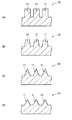
上記各実施の形態では、各部分電極32Aが矩形状となっていたが、各部分電極32Aの辺部(エッジ)の形状が非直線状となっていてもよい。例えば、各部分電極32Aは、他の部分電極32Aに隣接する辺部に、凹凸形状(凹凸部32B)を有していてもよい。凹凸部32Bは、例えば、図19に示したように、ジグザグ形状となっていてもよいし、例えば、図20(A)〜(D)に示したように、曲線形状、ランプ形状、台形状またはランダム形状となっていてもよい。
<3. Modification>
[First modification]
In each of the above embodiments, each
凹凸部32Bは、辺部に沿って配列された複数の凸部によって構成されている。互いに隣接する部分電極32Aの凹凸部32Bに含まれる各凸部は、例えば、図19,図20(A)〜(D)に示したように、互い違いに配置されている。凹凸部32Bに含まれる各凸部の先端は、例えば、図19,図20(A)〜(D)に示したように、隣接する他の凹凸部32Bによって形成される凹部の中に配置されている。互いに隣接する凹凸部32B同士の間に形成されるスリット部分の幅はできるだけ狭い方が好ましいが、後述のぼかし特性から、狭すぎてもあまり意味をなさない。従って、例えば、42インチサイズのディスプレイを12×6分割する場合に、部分電極32Aの幅をおよそ80mm程度としたときには、スリット部分の幅をおよそ10〜500μm程度とするのがよい。
The concavo-
このように、各部分電極32Aの辺部の形状が非直線状となっている場合には、各部分電極32Aの辺部において、下側電極32の、単位面積あたりの電極面積の変化が緩やかになる。これにより、上述の交差部分の全ての辺部において、光変調層34内に形成される散乱性と透明性との境界線が存在しない。従って、導光板10から取り出された光の輝度分布は、部分電極32Aの延在方向および部分電極32Aの延在方向と交差する方向の双方において緩やかに変化する。以上のことから、本変形例では、薄型化を阻害することなく、照明光における明暗の境界部分をより一層ぼかすことができる。また、本変形例では、各光源ブロック23を順次点灯させると共に、1または複数の部分電極32Aを駆動させることにより、単純マトリクス駆動を実現することができる。
As described above, when the shape of the side portion of each
また、例えば、図21に示したように、凹凸部32Bが、鋭角の先端を有する複数の凸部が配列されたジグザグ形状となっており、各凸部の少なくとも1つの輪郭が、先端を原点側とする略サインm乗の関数(mは偶数)となっていてもよい。このとき、各凸部の少なくとも1つの辺部の輪郭は、サインm乗の関数によって描かれる曲線の一部と一致している。なお、辺部の輪郭が厳密にサインm乗の関数をトレースしていなくてもよく、サインm乗の関数を概ねトレースしていてもよい。このように、凹凸部32Bに含まれる各凸部の少なくとも1つの輪郭が、先端を原点側とする略サインm乗の関数となっている場合には、その凸部の先端付近における下側電極32の電極面積の変化が上記の場合よりもさらに緩やかになる。これにより、透明と散乱の境界の明瞭さがより上記の場合よりもさらに低くなるので、導光板10から光が部分的に取り出されたときに、暗状態の部分と明状態の部分との明瞭さを上記の場合よりもさらに低くすることができる。その結果、照明光における明暗の境界部分を上記の場合よりもさらにぼかすことができる。
Further, for example, as shown in FIG. 21, the concavo-
なお、全ての部分電極32Aにおいて、辺部(エッジ)の形状が、必ずしも非直線状となっている必要はなく、例えば、図示しないが、互いに隣接する部分電極32Aのいずれか一方の辺部にだけ凹凸形状が設けられ、他方の辺部が直線状となっていてもよい。
Note that in all the
また、上記各実施の形態では、各部分電極32Aが矩形状となっていたが、各部分電極32Aが、他の部分電極32Aに隣接する辺部に、凹凸形状を有していてもよい。
Further, in each of the above embodiments, each
[第2変形例]
上記各実施の形態において、上側電極36または部分電極36Aがパターニングされていてもよい。これにより、照明光の面内輝度の均一化を行うことが出来る。さらに、電極の面積が減ることにより、上側電極36または部分電極36AがITOなどからなる場合に、電極による可視光の吸収を低減することが可能となる。
[Second modification]
In each of the above embodiments, the
上側電極36または部分電極36Aに対して、例えば、図22(A),(B)に示したように、複数の開口36Bが設けられていてもよい。このとき、開口36Bの密度が、例えば、図22(A),(B)に示したように、上側電極36全体または部分電極36A全体に関して均一となっている。開口36Bの形状は、例えば、図22(A),(B)に示したように円形状となっている。なお、開口36Bの形状は、それ以外の形状であってもよく、例えば、楕円形状、多角形状であってもよい。図22(A),(B)に示した例では、開口36Bの径rは、光源20からの距離に拘わらず一定(r=a1)となっており、単位面積当たりの開口36Bの数が、光源20からの距離に拘わらず一定となっている。
For the
なお、上側電極36または部分電極36Aのパターン密度(上側電極36または部分電極36Aのうち開口36B以外の部分の単位面積当たりの占有率)が上側電極36全体に関して光源20からの距離に応じて異なっていてもよい。例えば、開口36Bの密度(単位面積当たりの開口36Bの占有率)が、図23(A),(B)、図24(A),(B)に示したように、上側電極36全体に関して光源20からの距離に応じて異なっていてもよい。図23(A),(B)に示した例では、開口36Bの径rは、光源20からの距離に拘わらず一定(r=a1)となっており、単位面積当たりの開口36Bの数が、光源20からの距離が遠くなるにつれて少なくなっている。また、図24(A),(B)に示した例では、単位面積当たりの開口36Bの数は、光源20からの距離に拘わらず一定となっており、開口36Bの径rが、光源20からの距離が遠くなるにつれて小さくなっている。なお、図24(A),(B)には、光源20近傍の径rがa2となっており、光源20から最も離れたところの径rがa3(<a2)となっている場合が例示されている。従って、図23(A),(B)、図24(A),(B)のいずれの例においても、開口36Bの密度が、光源20からの距離が遠くなるにつれて疎になっている(小さくなっている)。言い換えると、上側電極36または部分電極36Aのパターン密度が、光源20からの距離が遠くなるにつれて密になっている(大きくなっている)。これにより、面内のあらゆる箇所における照明光の輝度を均一化することができる。
Note that the pattern density of the
なお、上側電極36または部分電極36Aのパターン密度は、必ずしも、上側電極36全体に関して光源20からの距離に応じて異なっている必要はない。例えば、上側電極36または部分電極36Aのパターン密度が、部分電極32Aとの対向部分ごとに、光源20からの距離に応じて異なっていてもよい。例えば、図25(A),(B)に示したように、開口36Bの径rが、光源20からの距離に拘わらず一定(r=a1)となっており、単位面積当たりの開口36Bの数が、部分電極32Aとの対向部分ごとに、光源20からの距離が遠くなるにつれて少なくなっていてもよい。また、例えば、図26(A),(B)に示したように、単位面積当たりの開口36Bの数は、光源20からの距離に拘わらず一定となっており、開口36Bの径rが、部分電極32Aとの対向部分ごとに、光源20からの距離が遠くなるにつれて小さくなっていてもよい。
Note that the pattern density of the
また、本変形例において、部分電極32Aに印加する電圧のデューティ比を光源20からの距離に応じて変化させてもよい。例えば、部分電極32Aに印加する電圧のデューティ比を光源20から遠ざかるにつれて大きくしてもよい。このようにした場合には、バックライト1の面内全体で白表示を行ったときに、面内全体の輝度を均一化することができ、また、バックライト1を部分点灯(部分駆動)したときに、上述の輝度突き上げを行うことができる。
In this modification, the duty ratio of the voltage applied to the
また、本変形例において、各部分電極32Aが、他の部分電極32Aに隣接する辺部に、凹凸形状(凹凸部32B)を有していてもよい。この場合に、上側電極36または部分電極36Aのパターン密度が、例えば、図27(A),(B)、図28(A),(B)に示したように、部分電極32Aとの対向部分ごとに、光源20からの距離に応じて異なっていてもよい。このとき、上側電極36または部分電極36Aにおいて、上側電極36または部分電極36Aのパターン密度が疎から密に切り替わる部分が、凹凸部32Bと対向する位置に設けられている。
Moreover, in this modification, each
図29(A),図30(A)は、下側電極32が、辺部に凹凸形状を有する複数の部分電極32Aからなり、上側電極36または部分電極36Aが、部分電極32Aとの対向部分ごとに光源20から離れるにつれてパターン密度が大きくなるようにパターニングが施されたものである場合であって、かつ、各部分電極32Aに印加する電圧を光源20からの距離に応じて変化させたときの散乱強度の一例を表したものである。図29(B),図30(B)は、各部分電極32Aに印加する電圧のデューティ比の一例を、図29(C),図30(C)は、上側電極36または各部分電極36AがITOからなる場合に、上側電極36または各部分電極36Aにおけるパターン密度の一例をそれぞれ表したものである。なお、図29(B),図30(B)では、デューティ比が緩やかに変化している様子が示されているが、これは、下側電極32のうち凹凸部32Bに対応する部分において、相対的に光源20に近い側に配置された部分電極32Aの密度(単位面積当たりの部分電極32Aの占有率)と、相対的に光源20から離れた位置に配置された部分電極32Aの密度(単位面積当たりの部分電極32Aの占有率)とが光源20からの距離に応じて緩やかに変化しており、印加される電圧の実質的なデューティ比が、互いに隣り合う2つの凹凸部32Bの単位面積当たりの占有率の比に応じて変化しているからである。
29A and 30A, the
図29(D),図30(D)は、上側電極36または部分電極36Aの構成の一例を表したものであり、図29(E),図30(E)は、各部分電極32Aの構成の一例を表したものである。図29(A)の散乱強度は、図29(B)のデューティ比と、図29(C)の上側電極36または部分電極36Aのパターン密度とを掛け合わせることにより得られ、図30(A)の散乱強度は、図30(B)のデューティ比と、図30(C)の上側電極36または部分電極36Aのパターン密度とを掛け合わせることにより得られる。
29D and 30D show an example of the configuration of the
図29(A)〜(E)および図30(A)〜(E)に記載のバックライト1,2では、各部分電極32Aの辺部のうち他の部分電極32Aと隣接する辺部が凹凸形状となっており、上側電極36または各部分電極36Aに複数の開口36Bが設けられている。さらに、開口36Bの数は、光源20からの距離に依らず一定となっており、開口36Bの径が、部分電極32Aとの対向領域ごとに、光源20からの距離に応じて小さくなっている。上側電極36または各部分電極36Aにおいて、パターン密度が疎の箇所と、パターン密度が密の箇所との境界が、凹凸部32Bと対向する領域内に配置されている。
In the
図29(A)〜(E)に記載のバックライト1,2では、パターン密度が疎の箇所と、パターン密度が密の箇所との境界において、パターン密度が急激に変化しており、散乱強度が、パターン密度が急激に変化する箇所(図中の破線で囲んだ箇所)で局所的に低下している。散乱強度の局所的な低下は、その低下量にも依るが、バックライト1,2から出力される照明光に明暗の縞を生じさせる場合がある。
In the
一方、図30(A)〜(E)に記載のバックライト1,2では、パターン密度が疎の箇所と、パターン密度が密の箇所との境界において、パターン密度が緩やかに変化しており、散乱強度も、パターン密度の変化に応じて緩やかに変化している。ここで、パターン密度が緩やかに減少し始める箇所(パターン密度が局所的に最も密になる箇所(図中のα))から、パターン密度が緩やかに上昇し始める箇所(パターン密度が局所的に最も疎になる箇所(図中のβ))までの区間S1が、互いに隣り合う2つの凹凸部32Bに含まれる凹部の底部32Xで囲まれる区間S2と対向する範囲内に収まっている。区間S1は、互いに隣り合う凹凸部32Bに含まれる凸部の頂部32Yで囲まれる区間S3と対向する範囲内に収まっていることがより好ましい。
On the other hand, in the
また、図29(A)〜(E),図30(A)〜(E)に記載のバックライト1,2において、各部分電極32Aの辺部のうち他の部分電極32Aと隣接する辺部が凹凸形状となっており、かつその凹凸形状の輪郭がサインm乗の関数となっている場合には、上側電極36または部分電極36Aのパターン密度が、図中のαからβまでの区間S1において、サインm乗の関数となっていることが好ましい。
Further, in the
ところで、本変形例において、下側電極32が、辺部に凹凸部32Bを有する複数の部分電極32Aからなり、上側電極36または部分電極36Aが、部分電極32Aとの対向部分ごとに光源20から離れるにつれてパターン密度が大きくなるようにパターニングが施されたものとなっている場合、図30(A)に対応する散乱強度は、デューティ比と、上側電極36または部分電極36Aのパターン密度とを掛け合わせた値となる。従って、散乱強度が図30(A)のように、下側電極32のうち凹凸形状32Bに対応する部分(区間S2または区間S3)で、光源20から遠ざかるにつれて単調に増大するためには、下記の式を満たすことが好ましい。なお、D1は図中のαの位置でのパターン密度であり、D2は図中のβの位置でのパターン密度である。D1/D2は、互いに隣り合う2つの凹凸部32Bの単位面積当たりの占有率の比である。
1<(D1/D2)<(β側の部分電極32Aに掛かる電圧のデューティ比(例えば図中の50%))/(α側の部分電極32Aに掛かる電圧のデューティ比(例えば図中の25%))
By the way, in this modification, the
1 <(D1 / D2) <(duty ratio of voltage applied to the β-side
なお、実際には、互いに隣り合う凹凸部32Bの間に、間隙(ジグザグのエッチング線)が存在するので、散乱強度が光源20からの距離に応じて滑らかに変化するためには、上側電極36または部分電極36Aのパターン密度が、この間隙を考慮したものになっていることが好ましい。例えば、図31(B)に示したように、間隙に対応する箇所にデューティ比の段差が生じている。従って、散乱強度の段差ができるだけ小さくなるようなパターン密度の段差が上側電極36または部分電極36Aに設けられていることが好ましい。具体的には、図31(C)に示したように、デューティ比の段差が生じている部分に対応して、パターン密度に段差が生じていることが好ましい。このとき、パターン密度は、段差において、(D×2/P)×100[%]程度、増加していることが好ましい。なお、Dは間隙の幅であり、Pは間隙のジグザグのピッチである。また、図32の線分Aに示したように、パターン密度の段差が、緩やかになっていることが好ましい。さらに、図32の線分Bに示したように、パターン密度の大きさを全体的に減少させることが好ましい。例えば、各開口36Bの径を大きくすることで、パターン密度の大きさを全体的に減少させることが可能である。これにより、各部分電極32Aおよび上側電極36または部分電極36AがITOなどからなる場合に、電極による可視光の吸収を低減することが可能となる。
Actually, since there is a gap (zigzag etching line) between the concavo-
[第3変形例]
上記各実施の形態において、各部分電極32Aが、他の部分電極32Aに隣接する辺部に、凹凸形状(凹凸部32B)を有し、さらに、パターニングされていてもよい。各部分電極32Aに対して、例えば、図33(A),(B)に示したように、複数の開口32Cが設けられていてもよい。このとき、開口32Cが、例えば、図33(A)に示したように、部分電極32Aのうち凹凸部32B以外の部分にだけ形成されていてもよいし、例えば、図33(B)に示したように、凹凸部32Bを含む部分電極32A全体に形成されていてもよい。いずれの場合においても、下側電極32のうち凹凸部32Bを含む部分における開口32Cおよびスリット部の密度と、部分電極32Aのうち凹凸部32B以外の部分における開口32Cの密度とが互いに等しくなっていることが好ましい。
[Third Modification]
In each of the above embodiments, each
また、例えば、図34(A)に示したように、部分電極32Aの延在方向に延在する複数の帯状の開口32Eが設けられていたり、例えば、図34(B)に示したように、部分電極32Aの延在方向と交差(もしくは直交)する方向に延在する複数の帯状の開口32Eが設けられていたりしてもよい。これらの場合においても、下側電極32のうち凹凸部32Bを含む部分における開口32Eおよびスリット部の密度(以下、便宜的に「密度A」と称する。)と、部分電極32Aのうち凹凸部32B以外の部分における開口32Eの密度(以下、便宜的に「密度B」と称する。)とが互いに等しくなっていることが好ましい。
Further, for example, as shown in FIG. 34A, a plurality of strip-shaped
例えば、密度Aが密度Bよりも小さい場合であって、かつ下側電極32および上側電極36に電圧を印加しない時に光変調セル30−1が透明状態となり、下側電極32および上側電極36に電圧を印加した時に光変調セル30−1が散乱状態となるとき、全面点灯状態で、凹凸部32Bに対応する部分が暗くなってしまう。また、例えば、密度Aが密度Bよりも小さい場合であって、かつ下側電極32および上側電極36に電圧を印加しない時に光変調セル30−1が散乱状態となり、下側電極32および上側電極36に電圧を印加した時に光変調セル30−1が透明状態となるとき、全面点灯状態で、凹凸部32Bに対応する部分が明るくなってしまう。
For example, when the density A is smaller than the density B and no voltage is applied to the
なお、各部分電極32Aがパターニングされ、各部分電極32Aの面積が減ると、下側電極32および上側電極36に電圧を印加しない時に光変調セル30−1が透明状態となり、下側電極32および上側電極36に電圧を印加した時に光変調セル30−1が散乱状態となるとき、散乱する面積が減少するので、光取り出し能力が低下する。これでは、ITOの面積を減らして吸収量を減少させ輝度を向上させる効果が十分に得られない。よって、パターニングにより各部分電極32Aの面積を減らす場合は、光変調層34の単位面積当たりの散乱強度を強くすることが好ましい。散乱強度を強くする方法としては、駆動電圧を高くする、光変調層の厚みを厚くする、バルクと微粒子の組成比を変える、などが考えられる。また、光の吸収率がより小さなITOを用いた場合には、ITOの面積の削減量があまり大きくなくても、光取り出し効率(照度)を高くすることができる。また、光の吸収率がより小さなITOを用いた場合であっても、光変調層34の単位面積当たりの散乱強度を強くすることが好ましい。
When each
図35は、ITOの面積の削減量と相対照度との関係の一例を表したものである。図35中の線分Aは、光変調層34の単位面積当たりの散乱強度を変更せずに(増大させずに)、ITOの面積だけを減らしたときの結果である。図35中の線分B,Cは、散乱する面積が減少しても光取り出し能力が一定に保たれるように、光変調層34の単位面積当たりの散乱強度を増大させたときの結果である。図35中の線分Aと線分Bは、550nmでのITOの光の吸収率(垂直から5度傾けて光を入射させた場合の吸収率)が0.9%となっているときの結果であり、図35中の線分Cは、550nmでのITOの光の吸収率(垂直から5度傾けて光を入射させた場合の吸収率)が0.3%となっているときの結果である。
FIG. 35 shows an example of the relationship between the reduction amount of the ITO area and the relative illuminance. A line segment A in FIG. 35 is a result when only the area of ITO is reduced without changing (increasing) the scattering intensity per unit area of the
なお、図35の縦軸は、仮に吸収が無いとした場合のITOの照度を100%とした場合の相対的な照度の値であり、横軸はITOの面積の削減量である。また、図35の結果は、下記の条件で数値計算することにより得られたものである。
導光板:n=1.49,厚み5mm
透明基板:n=1.53,厚み0.1mm
電極(ITO):n=2.0
光変調層:面に垂直に入射する光に対してヘイズ33%(実測値)の散乱
構成:導光板の裏面に光変調素子、反射シートあり、
導光板の上面に拡散シート、プリズムシートあり
バックライトのサイズ:40インチ
The vertical axis in FIG. 35 is a relative illuminance value when the illuminance of ITO is assumed to be 100% when there is no absorption, and the horizontal axis is a reduction amount of the area of ITO. Moreover, the result of FIG. 35 was obtained by calculating numerically on the following conditions.
Light guide plate: n = 1.49,
Transparent substrate: n = 1.53, thickness 0.1 mm
Electrode (ITO): n = 2.0
Light modulation layer: scattering of
There is a diffusion sheet and a prism sheet on the upper surface of the light guide plate. Backlight size: 40 inches
図35の線分Aから、光変調層34の単位面積当たりの散乱強度があまり強くない場合には、ITOの面積を減らして吸収量を減少させても、輝度を向上させる効果を十分に得ることができない場合があることがわかる。また、図35の線分Bから、光変調層34の単位面積当たりの散乱強度を強くした上で、ITOの面積を減らした場合には、輝度を向上させる効果を十分に得ることができることがわかる。また、図35の線分Cから、光の吸収率がより小さなITOを用いた場合には、ITOの面積の削減量があまり大きくなくても、光取り出し効率(照度)を高くすることができることがわかる。さらに、図35の線分Cから、光の吸収率がより小さなITOを用いた場合であっても、光変調層34の単位面積当たりの散乱強度を強くした方が、輝度を向上させる効果を十分に得ることができることがわかる。
When the scattering intensity per unit area of the
また、部分電極32Aに複数の開口32Eが設けられている場合に、例えば、図36(A)に示したように、開口32Eと交差(もしくは直交)する方向に延在する金属線32Gが、部分電極32Aごとに1本ずつ設けられていてもよい。これにより、部分電極32Aに複数の開口32Eを設けたことによる抵抗値の増大を抑制することができる。金属線32Gによって照明光にムラが生じないことが好ましいことから、例えば導光板10の厚みが5mmで光変調素子30が導光板10の背面に配置され、導光板10上に拡散シート、プリズムシート、偏光分離シートが設けられている場合、金属線32Gの幅は200μm以下であることが好ましい。
Further, when a plurality of
また、開口32Eと交差(もしくは直交)する方向に延在する金属線32Gを、部分電極32Aごとに1本ずつ設ける場合には、例えば、図36(B)に示したように、部分電極32Aの延在方向と交差(もしくは直交)する方向に延在する複数の帯状の間隙32Fを設けることが可能である。パターニング加工の容易性を考えると、開口32Eよりも間隙32Fを部分電極32Aに設ける方が優れている。
When one
開口32C、間隙32Fの配置は、他の周期構造(凸部11や、開口36B)とのモアレを回避する必要がある場合には、ランダムであることが望ましい。開口32C、間隙32Fの配置が周期的である場合は、開口32C、間隙32Fのピッチを、他の周期構造のピッチ(例えば凸部11や開口36Bのピッチ)の反整数(1/2を除く)倍もしくは反整数(1/2を除く)分の1とすることが好ましい。ただし、同一部材内にある周期構造(32Bのジグザグ構造)に対しては位置合わせが可能であるので、開口32C、間隙32Fのピッチを、同一部材内にある周期構造のピッチの整数倍もしくは整数分の1とすることが好ましい。
The arrangement of the
[第4変形例]
上記各実施の形態において、各部分電極32Aおよび上側電極36または部分電極36Aに対して、開口32C,36Bが形成されていてもよい。これにより、各部分電極32Aおよび上側電極36または部分電極36AがITOなどからなる場合に、電極による可視光の吸収を低減することが可能となる。
[Fourth modification]
In each of the above embodiments,
この場合に、部分電極32Aに形成された開口32Cと、上側電極36または部分電極36Aに形成された開口36Bとが、少なくとも一部分で互いに対向していることが好ましく、例えば、図37に示したように、互いに正対している(または向き合っている)ことがより好ましい。なお、図37に示したように開口32Cと開口36Bとが互いに正対する(または向き合う)ためには、光変調素子30の法線方向から見たときに、開口32Cの位置と開口36Bの位置とが一致していることが必要である。このとき、開口32Cと開口36Bとが互いに同一形状、同一面積となっていることが好ましい。
In this case, it is preferable that the
ここで、各部分電極32Aおよび上側電極36または部分電極36Aに電圧を印加しない時に光変調セル30−1が透明状態となり、各部分電極32Aおよび上側電極36または部分電極36Aに電圧を印加した時に光変調セル30−1が散乱状態となる場合に、部分電極32Aと、上側電極36または部分電極36Aとが互いに対向する部分だけで、光変調層34は散乱状態になる。そのため、部分電極32Aのうち上側電極36または部分電極36Aと対向しない部分や、上側電極36または部分電極36Aのうち部分電極32Aと対向しない部分については、電圧を印加しても透明と散乱の切り替えが出来ない。従って、各部分電極32Aおよび上側電極36または部分電極36Aの面積を減少させつつ散乱強度を最大限に確保するには、図37に示したように、光変調素子30を光変調素子30の法線方向から見たときに、開口32Cと開口36Bとが互いに重なり合っていることが好ましい。
Here, when no voltage is applied to each
[第5変形例]
上記実施の形態等では、光変調素子30,60は、導光板10の背後(下面)に空気層を介さずに密着して接合されていたが、例えば、図38に示したように、導光板10の上面に空気層を介さずに密着して接合されていてもよい。また、光変調素子30,60は、例えば、図39に示したように、導光板10の内部に設けられていてもよい。ただし、この場合でも、光変調素子30,60は、導光板10と空気層を介さずに密着して接合されていることが必要である。
[Fifth Modification]
In the above embodiment and the like, the
[第6変形例]
また、上記実施の形態等では、導光板10の上に特に何も設けられていなかったが、例えば、図40に示したように、光学シート70(例えば、拡散板、拡散シート、レンズフィルム、偏光分離シートなど)を設けてもよい。このようにした場合には、導光板10から斜め方向に射出した光の一部が正面方向に立ち上がるので、変調比を効果的に向上させることができる。
[Sixth Modification]
Further, in the above embodiment and the like, nothing was provided on the
<4.実施例>
次に、上記各実施の形態のバックライト1,2の実施例について、比較例と対比して説明する。
<4. Example>
Next, examples of the
図41〜図43は、比較例に係るバックライト100が光を出力している様子を模式的に表したものである。図44は、実施例に係るバックライト1,2が光を出力している様子を模式的に表したものである。比較例に係るバックライト100では、導光板として、上面が平坦面となっているものを用い、実施例に係るバックライト1,2では、導光板として、上面に複数の凸部11が設けられたものを用いた。各凸部11は、光源20に近づくにつれて高さが低くなる形状となっており、具体的には、図45(A)に示したように、高さが最も高い部分において、断面形状が、上底293μm、下底327μm、斜面傾き86.7度、高さ300μmの台形形状となっており、凸部11のピッチが400μmとなっている。また、凸部11の高さが、図45(B)に示したように、光入射面10Aからの距離が30mmより大きく130mmよりも小さな箇所において、ほぼ線形で変化しており、光入射面10Aからの距離が0mm以上30mm以下の箇所において、ほぼゼロとなっており、光入射面10Aからの距離が130mm以上の箇所において、最大値で一定となっている。なお、各凸部11の断面形状が、例えば、図46に示したようなシリンドリカル形状となっていてもよい。この場合には、各凸部11を成型する際の転写性が良くなるので、各凸部11を溶融押し出し法などで作成することが容易となる。以下に、比較例に係るバックライト100および実施例に係るバックライト1,2において共通する構成を示す。
導光板:厚み5mm、サイズ300×250mm
下側電極:ITO膜、幅83mm、3列
上側電極:ITO膜、幅75mm、4行
電圧:100Hz、140Vppのパルス電圧
光源:白色LED
41 to 43 schematically show how the
Light guide plate: thickness 5mm, size 300x250mm
Lower electrode: ITO film, width 83 mm, 3 rows Upper electrode: ITO film, width 75 mm, 4 rows Voltage: 100 Hz, pulse voltage of 140 Vpp Light source: White LED
図41では、全ての光源ブロック23をオン(点灯)させ、図42〜図44では、3行目の光源ブロック23だけをオンさせた。図41、図42では、3行目の光変調セル30−1だけを散乱領域30Bにし、それ以外の光変調セル30−1を透過領域30Aにした。図43、図44では、全ての光変調セル30−1を散乱領域30Bにした。
In FIG. 41, all the light source blocks 23 are turned on (lighted), and in FIGS. 42 to 44, only the light source blocks 23 in the third row are turned on. 41 and 42, only the light modulation cell 30-1 in the third row is used as the
図41、図42、図44では、3行目の光変調セル30−1から光L1が出力され、図43では、各光変調セル30−1のうち3行目の光源ブロック23から出力された光が通過した部分から光L1が出力された。図41の線分A,B,Cに対応する部分での照明光の輝度分布を図47に示し、図42の線分A,B,Cに対応する部分での照明光の輝度分布を図48に示し、図43の線分A,B,Cに対応する部分での照明光の輝度分布を図49に示し、図44の線分A,B,Cに対応する部分での照明光の輝度分布を図50に示した。なお、図47〜50では、線分A,B,Cがそれぞれ、同一バックライトで測定された結果であることから、縦軸の値がAの最大値で規格化されている。
41, 42, and 44, the light L1 is output from the light modulation cell 30-1 in the third row, and in FIG. 43, the light L1 is output from the
図41、図47では、境界での輝度変化が急峻であり、見た目にも境界が視認できた。さらに、図41、図47では、光源20全体を点灯しているので、輝度は高い。しかし、導光板上面が平坦面となっているために、光源20から離れるにつれて光入射面10Aと平行な方向への広がりも大きく、駆動していない部分の輝度が高くなった。図42、図48でも、境界での輝度変化が急峻であり、見た目にも境界が視認できた。さらに、図42、図48では、光源20から離れるにつれて輝度の減少が大きくなった。図43、図49では、光源20から離れるにつれて輝度分布が平坦になっており、部分点灯(部分駆動)にはならなかった。一方で、図44、図50では、コントラストが向上しつつ、境界も滑らかになっており、照明光における明暗の境界部分をぼかした部分点灯(部分駆動)を実現することができた。
In FIGS. 41 and 47, the luminance change at the boundary is steep, and the boundary can be visually recognized. Furthermore, in FIG. 41 and FIG. 47, since the entire
図51〜図53は、比較例に係るバックライト100が光を出力している様子を模式的に表したものである。図54は、実施例に係るバックライト1,2が光を出力している様子を模式的に表したものである。比較例に係るバックライト100では、導光板として、上面が平坦面となっているものを用い、実施例に係るバックライト1,2では、導光板として、上面に複数の凸部11が設けられているものを用いた。なお、比較例に係るバックライト100および実施例に係るバックライト1,2において共通する構成は、上記と同一である。
51 to 53 schematically show how the
図51では、全ての光源ブロック23をオンさせ、図52〜図54では、3行目の光源ブロック23だけをオンさせた。図51、図52では、2列3行の部分に対応する光変調セル30−1だけを散乱領域30Bにし、それ以外の光変調セル30−1を透過領域30Aにした。図53、図54では、2列目の光変調セル30−1だけを散乱領域30Bにし、それ以外の光変調セル30−1を透過領域30Aにした。
In FIG. 51, all the light source blocks 23 are turned on. In FIGS. 52 to 54, only the light source blocks 23 in the third row are turned on. 51 and 52, only the light modulation cell 30-1 corresponding to the portion of 2 columns and 3 rows is used as the
図51、図52、図54では、2列×3行の部分に対応する光変調セル30−1から光L1が出力され、図53では、2列目の光変調セル30−1のうち3行目の光源ブロック23から出力された光が通過した部分から光L1が出力された。図51〜図54の線分A,B,C,Dに対応する部分での照明光の輝度分布を図55に示した。なお、図55では、線分A,B,C,Dがそれぞれ、別々のバックライトで測定された結果であることから、線分A,B,C,Dごとに、縦軸の値が最大値で1となるように規格化されている。
51, 52, and 54, the light L1 is output from the light modulation cell 30-1 corresponding to the portion of 2 columns × 3 rows, and in FIG. 53, 3 of the light modulation cells 30-1 in the second column. The light L1 was output from the portion through which the light output from the
図51、図55の線分Aでは、境界での輝度変化が急峻であり、見た目にも境界が視認できた。さらに、図51、図55の線分Aでは、導光板上面が平坦面となっているために、光源20から離れるにつれて光入射面10Aと平行な方向への広がりも大きく、駆動していない部分の輝度が高くなった。図52、図55の線分Bでも、境界での輝度変化が急峻であり、見た目にも境界が視認できた。図53、図55の線分Cでは、光入射面10Aと平行な方向への広がりが大きく、部分点灯(部分駆動)にはならなかった。一方で、図54、図55の線分Dでは、コントラストが向上しつつ、境界も滑らかになっており、照明光における明暗の境界部分をぼかした部分点灯(部分駆動)を実現することができた。
In line segment A of FIGS. 51 and 55, the luminance change at the boundary is steep, and the boundary can be visually recognized. Further, in the line segment A of FIGS. 51 and 55, since the upper surface of the light guide plate is a flat surface, as the distance from the
図56(A),(B)は、実施例に係るバックライト1,2において、光変調層30,60を全面散乱状態にするとともに、1つの側面に設けられた各点状光源21を全て点灯したときの面内輝度の計測値の一例を表したものである。なお、図56(A),(B)には、光源20近傍の90mm×120mmのエリアの面内輝度が示されている。図56(A),(B)では、共に、導光板10として、厚さ5mm、サイズ300mm×250mmのものを用い、さらに、上面に複数の凸部11が設けられているものを用いた。図56(A)では、各凸部11の高さが図45(B)に示したように変化しており、かつ各凸部11が図45(A)に示した断面形状を有する導光板10を用いた。図56(B)では、各凸部11の高さが300μmで一定となっており、かつ各凸部11が図45(A)に示した断面形状を有する導光板10を用いた。
56 (A) and 56 (B) show that the light modulation layers 30 and 60 are all scattered in the
図56(A),(B)から、各凸部11の高さに変化が無い場合には、各凸部11の高さに変化がある場合と比べて、点状光源21近傍の明るい領域が長く伸びており、さらに、その明るい領域同士の間の暗い領域も長く伸びていることがわかった。そのため、各凸部11の高さに変化が無い場合には、明暗が強く出ている領域が広範囲に及んでおり、画質が劣化することがわかる。
56 (A) and 56 (B), when there is no change in the height of each
図57は、実施例に係るバックライト1,2と、比較例に係るバックライト100とにおいて、光変調層30,60を全面散乱状態にするとともに、1つの側面に設けられた各点状光源21を全て点灯したときの画面中央での輝度の計測値の一例を表したものである。実施例では、導光板10として、厚さ4mm、32インチサイズのものを用い、さらに、上面に複数の凸部11が設けられているものを用いた。実施例では、導光板10として、凸部11が頂角90度の三角プリズム形状となっており、凸部11のピッチが50μmとなっているものを用いた。一方、比較例では、導光板として、厚さ4mmのものを用い、さらに、上面が平坦となっているものを用いた。実施例、比較例ともに、点状光源21を導光板の2辺に設け、さらに、点状光源21として白色LEDを用いた。
FIG. 57 shows each of the point light sources provided on one side surface of the
図57から、凸部11が頂角90度の三角プリズム形状となっている導光板10を用いた場合には、上面が平坦となっている導光板を用いた場合と比べて、輝度が約11%向上することがわかった。
From FIG. 57, when the
図58,図59は、比較例に係るバックライト100が光を出力している様子を模式的に表したものである。図60は、実施例に係るバックライト1,2が光を出力している様子を模式的に表したものである。比較例に係るバックライト100を下記の条件で構成し、実施例に係るバックライト1,2を下記の条件で構成した。
(バックライト100)
導光板:厚み5mm、サイズ300×250mm、上面は平坦面
下側電極:ITO膜、幅83mm、3列
上側電極:ITO膜、幅75mm、4行、開口なし
電圧:100Hz、140Vppのパルス電圧
光源:白色LED
(バックライト1,2)
導光板:厚み5mm、サイズ300×250mm、上面に凸部11あり
下側電極:ITO膜、幅83mm、3列
上側電極:ITO膜、幅75mm、4行、
100μm〜700μmの範囲内のサイズの複数の開口あり
単位面積当たりの開口の数は一定
開口の径が下側電極との対向部分ごとに、光源からの距離が遠くなるに
つれて小さくなっている
パターン密度は図61の線分aに示したようになっている
電圧:100Hz、140Vppのパルス電圧
光源:白色LED
58 and 59 schematically show how the
(Backlight 100)
Light guide plate:
(
Light guide plate:
Multiple openings with sizes in the range of 100 μm to 700 μm
The number of openings per unit area is constant
The distance from the light source becomes longer for each part of the opening facing the lower electrode.
Getting smaller
The pattern density is as shown in line segment a of FIG. 61. Voltage: 100 Hz, pulse voltage of 140 Vpp Light source: White LED
図58〜図60では、全ての光源ブロック23をオンさせ、さらに、全ての光変調セル30−1を散乱領域30Bにした。図58では、全ての部分電極32Aに対して100%のデューティ比で電圧を印加した。図59では、1列目の部分電極32Aに対して28%のデューティ比で電圧を印加し、2列目の部分電極32Aに対して45%のデューティ比で電圧を印加し、3列目の部分電極32Aに対して100%のデューティ比で電圧を印加した。図60では、1列目の部分電極32Aに対して22%のデューティ比で電圧を印加し、2列目の部分電極32Aに対して40%のデューティ比で電圧を印加し、3列目の部分電極32Aに対して100%のデューティ比で電圧を印加した。
58 to 60, all the light source blocks 23 are turned on, and all the light modulation cells 30-1 are set to the
図58〜図60では、全ての光変調セル30−1から光L1が出力された。図58〜図60の線分A,B,Cに対応する部分での照明光の輝度分布を図62に示した。また、図60において、下側電極の辺部に対して以下に示した特徴を有する凹凸形状を形成し、さらに、上側電極のパターン密度の変化を図61の線分bに示したように緩やかにしたときの、線分Dに対応する部分での照明光の輝度分布と、図58,図59の線分A,Bに対応する部分での照明光の輝度分布とを図63に示した。なお、パターン密度の変化を線分bに示したように緩やかにするために、上側電極のうちジグザグの凹凸形状に対応する部分のパターン密度の変化を緩やかにするとともに、上側電極のパターン密度に対して、互いに隣り合う凹凸形状の間に形成される間隙を考慮した補正を行った。さらに、上側電極に設けた開口の径を大きくして、上側電極のパターン密度を図61の線分aの場合と比べて、2/3程度にまで減らした。このとき、D1を0.507とし、D2を0.337とした。従って、D1/D2が1.50となり、D1/D2が1よりも大きく、100%/40%よりも小さく、40%/22%よりも小さくなっている。
(下側電極の辺部の凹凸形状)
輪郭:サイン2乗の関数
互いに隣り合う凹凸形状の間に形成される間隙の幅:0.1mm
凹凸形状に含まれる各凸部の幅:60mm
凹凸形状に含まれる各凸部のピッチ:1.9mm
58 to 60, the light L1 is output from all the light modulation cells 30-1. FIG. 62 shows the luminance distribution of the illumination light at the portions corresponding to the line segments A, B, and C in FIGS. Further, in FIG. 60, a concavo-convex shape having the following characteristics is formed on the side portion of the lower electrode, and the change in the pattern density of the upper electrode is gradual as shown by the line b in FIG. FIG. 63 shows the luminance distribution of the illumination light at the portion corresponding to the line segment D and the luminance distribution of the illumination light at the portions corresponding to the line segments A and B in FIGS. . In order to moderate the change in pattern density as shown by line b, the pattern density of the upper electrode corresponding to the zigzag uneven shape is moderated and the pattern density of the upper electrode is reduced. On the other hand, correction was performed in consideration of the gap formed between the uneven shapes adjacent to each other. Furthermore, the diameter of the opening provided in the upper electrode was increased, and the pattern density of the upper electrode was reduced to about 2/3 compared with the case of the line segment a in FIG. At this time, D1 was set to 0.507, and D2 was set to 0.337. Therefore, D1 / D2 is 1.50, and D1 / D2 is larger than 1, smaller than 100% / 40%, and smaller than 40% / 22%.
(Uneven shape on the side of the lower electrode)
Outline: Function of sine square Width of gap formed between adjacent concave and convex shapes: 0.1 mm
Width of each convex part included in the concavo-convex shape: 60 mm
Pitch of each convex part included in the uneven shape: 1.9 mm
図58、図62の線分Aでは、デューティ比が全て同じであり、全ての光変調セル30−1において散乱強度が同じであることから、光源20近くの列で光が多く取り出され、明るさが均一化されていない。図59、図62の線分Bでは、光源20から遠ざかるにつれデューティ比が大きくなるように設定されているので、明るさの均一性は図58、図62の線分Aの場合に比べ改善した。しかし、図59、図62の線分Bでは、上側電極に対して輝度均一化のための開口が設けられていないので、列内において光源20に近い領域が明るくなっており、明るさが均一化されていない。一方、図60、図62の線分Cでは、光源20から遠ざかるにつれデューティ比が大きくなるように設定されており、さらに上側電極に対して輝度均一化のための開口が設けられているので、明るさが均一となっている。さらに、図63の線分Dでは、下側電極の辺部に対して、輪郭がサイン2乗となるジグザグの凹凸形状を形成したので、明るさがより一層、均一となっている。
58 and 62, since the duty ratios are all the same and the scattering intensity is the same in all the light modulation cells 30-1, a large amount of light is extracted in the column near the
図64,図65は、比較例に係るバックライト100が光を出力している様子を模式的に表したものである。図66は、実施例に係るバックライト1,2が光を出力している様子を模式的に表したものである。比較例に係るバックライト100を下記の条件で構成し、実施例に係るバックライト1,2を下記の条件で構成した。
(バックライト100)
導光板:厚み5mm、サイズ300×250mm、上面は平坦面
下側電極:ITO膜、幅83mm、3列
上側電極:ITO膜、幅75mm、4行、開口なし
電圧:100Hz、140Vppのパルス電圧
光源:白色LED
(バックライト1,2)
導光板:厚み5mm、サイズ300×250mm、上面に凸部あり
下側電極:ITO膜、幅83mm、3列
上側電極:ITO膜、幅75mm、4行、
100μm〜700μmの範囲内のサイズの複数の開口あり
単位面積当たりの開口の数は一定
開口の径が下側電極との対向部分ごとに、光源からの距離が遠くなるに
つれて小さくなっている
電圧:100Hz、140Vppのパルス電圧
光源:白色LED
64 and 65 schematically show how the
(Backlight 100)
Light guide plate:
(
Light guide plate:
Multiple openings with sizes in the range of 100 μm to 700 μm
The number of openings per unit area is constant
The distance from the light source becomes longer for each part of the opening facing the lower electrode.
Voltage decreases: 100 Hz, 140 Vpp pulse voltage Light source: White LED
図64では、全ての光源ブロック23をオンさせた。図65,図66では、3行目の光源ブロック23だけをオンさせ、それ以外の光源ブロック23をオフさせた。図64〜図66では、3行目の光変調セル30−1だけを散乱領域30Bにし、それ以外の光変調セル30−1を透過領域30Aにした。図64〜図66では、全ての部分電極32Aに対して100%のデューティ比で電圧を印加した。
In FIG. 64, all the light source blocks 23 are turned on. 65 and 66, only the
図64〜図66では、3行目の光変調セル30−1から光L1が出力された。図64〜図66の線分A,B,Cに対応する部分での照明光の輝度分布を図67に示した。また、図66において、下側電極の辺部に対して、輪郭がサイン2乗となるジグザグの凹凸形状を形成し、さらに、下側電極のうちジグザグの凹凸形状に対応する部分のパターン密度の変化を図30(A)に示したように緩やかにしたときに、線分Dに対応する部分での照明光の輝度分布と、図64,図65の線分A,Bに対応する部分での照明光の輝度分布とを図68に示した。なお、図67では、線分A,B,Cがそれぞれ、別々のバックライトで測定された結果であることから、線分A,B,Cごとに、縦軸の値が最大値で1となるように規格化されている。また、図68では、線分A,B,Dがそれぞれ、別々のバックライトで測定された結果であることから、線分A,B,Dごとに、縦軸の値が最大値で1となるように規格化されている。 64 to 66, the light L1 is output from the light modulation cell 30-1 in the third row. FIG. 67 shows the luminance distribution of the illumination light at the portions corresponding to the line segments A, B, and C in FIGS. In FIG. 66, a zigzag uneven shape whose outline is a sign square is formed on the side portion of the lower electrode, and the pattern density of the portion corresponding to the zigzag uneven shape of the lower electrode is formed. When the change is moderated as shown in FIG. 30A, the luminance distribution of the illumination light in the portion corresponding to the line segment D and the portions corresponding to the line segments A and B in FIGS. FIG. 68 shows the luminance distribution of the illumination light. In FIG. 67, line segments A, B, and C are the results of measurement with separate backlights, and therefore, the value of the vertical axis is 1 at the maximum for each of line segments A, B, and C. It is standardized to be. In FIG. 68, line segments A, B, and D are the results of measurement with separate backlights, and therefore the value of the vertical axis is 1 at the maximum for each of line segments A, B, and D. It is standardized to be.
図64、図67の線分Aでは、境界での輝度変化が急峻であり、見た目にも境界が視認できた。さらに、図64、図67の線分Aでは、導光板上面が平坦面となっているために、光源20から離れるにつれて光入射面10Aと平行な方向への広がりも大きく、駆動していない部分の輝度が高くなった。図65、図67の線分Bでも、境界での輝度変化が急峻であり、見た目にも境界が視認できた。一方、図66、図67の線分Cでは、コントラストが向上しつつ、境界も滑らかになっており、照明光における明暗の境界部分をぼかした部分点灯(部分駆動)を実現することができた。さらに、図68の線分Dでも同様に、コントラストが向上しつつ、境界も滑らかになっており、照明光における明暗の境界部分をぼかした部分点灯(部分駆動)を実現することができた。
In the line segment A in FIGS. 64 and 67, the luminance change at the boundary is steep, and the boundary can be visually recognized. 64 and 67, since the upper surface of the light guide plate is a flat surface, the portion extending in a direction parallel to the
図69〜図71は、実施例に係るバックライト1,2が光を出力している様子を模式的に表したものである。実施例に係るバックライト1,2を下記の条件で構成した。
導光板:厚み5mm、サイズ300×250mm、上面に凸部あり
下側電極:ITO膜、幅83mm、3列
輪郭がサイン2乗となるジグザグの凹凸形状あり
上側電極:ITO膜、幅75mm、4行、
100μm〜700μmの範囲内のサイズの複数の開口あり
単位面積当たりの開口の数は一定
開口の径が下側電極との対向部分ごとに、光源からの距離が遠くなるに
つれて小さくなっている
電圧:100Hz、140Vppのパルス電圧
光源:白色LED
69 to 71 schematically show how the
Light guide plate:
There are zigzag irregularities with an outline of a sign square. Upper electrode: ITO film, width 75 mm, 4 rows,
Multiple openings with sizes in the range of 100 μm to 700 μm
The number of openings per unit area is constant
The distance from the light source becomes longer for each part of the opening facing the lower electrode.
Voltage decreases: 100 Hz, 140 Vpp pulse voltage Light source: White LED
図69〜図71では、全ての光源ブロック23をオンさせた。図69では、3列目の光変調セル30−1だけを散乱領域30Bにし、それ以外の光変調セル30−1を透過領域30Aにした。図70では、2列目の光変調セル30−1だけを散乱領域30Bにし、それ以外の光変調セル30−1を透過領域30Aにした。図71では、1列目の光変調セル30−1だけを散乱領域30Bにし、それ以外の光変調セル30−1を透過領域30Aにした。図69〜図71では、全ての部分電極32Aに対して100%のデューティ比で電圧を印加した。
69 to 71, all the light source blocks 23 are turned on. In FIG. 69, only the light modulation cells 30-1 in the third row are used as the
図69では、3列目に対応する光変調セル30−1から光L1が出力され、図70では、2列目に対応する光変調セル30−1から光L1が出力され、図71では、1列目に対応する光変調セル30−1から光L1が出力された。図69〜図71の線分A,B,Cに対応する部分での照明光の輝度分布と、図63の線分Dの輝度分布とを図72に示した。 In FIG. 69, the light L1 is output from the light modulation cell 30-1 corresponding to the third column, in FIG. 70, the light L1 is output from the light modulation cell 30-1 corresponding to the second column, Light L1 was output from the light modulation cell 30-1 corresponding to the first column. FIG. 72 shows the luminance distribution of the illumination light in the portions corresponding to the line segments A, B, and C in FIGS. 69 to 71 and the luminance distribution of the line segment D in FIG.
図69〜図71、図72の線分A〜Cでは、ともに、境界が滑らかになっており、照明光における明暗の境界部分をぼかした部分点灯(部分駆動)を実現することができた。さらに、図72の線分Aでは、図72の線分Dと比べて、輝度が1.5倍となっており、図72の線分Bでは、図72の線分Dと比べて、輝度が1.6倍となっており、図72の線分Cでは、図72の線分Dと比べて、輝度が2.2倍となっており、輝度が向上した。 In FIGS. 69 to 71 and line segments A to C in FIG. 72, the boundaries are smooth, and partial lighting (partial drive) in which the bright and dark boundary portions in the illumination light are blurred can be realized. Further, the luminance of the line segment A in FIG. 72 is 1.5 times that of the line segment D of FIG. 72, and the luminance of the line segment B of FIG. 72 is higher than that of the line segment D of FIG. Is 1.6 times, and the luminance of the line segment C in FIG. 72 is 2.2 times that of the line segment D in FIG.
図73は、比較例に係るバックライト100が光を出力している様子を模式的に表したものである。比較例に係るバックライト100を下記の条件で構成した。
導光板:厚み5mm、サイズ300×250mm、上面は平坦面
下側電極:ITO膜、幅83mm、3列
上側電極:ITO膜、幅75mm、4行、開口なし
電圧:100Hz、140Vppのパルス電圧
光源:白色LED
FIG. 73 schematically shows how the
Light guide plate:
図73では、全ての光源ブロック23をオンした。さらに、2列目の光変調セル30−1を散乱領域30Bにし、それ以外の光変調セル30−1を透過領域30Aにした。図73では、全ての部分電極32Aに対して100%のデューティ比で電圧を印加した。
In FIG. 73, all the light source blocks 23 are turned on. Furthermore, the light modulation cells 30-1 in the second row are used as the
図73では、2列目に対応する光変調セル30−1から光L1が出力された。図73の線分Aに対応する部分での照明光の輝度分布と、図62の線分Bの輝度分布とを図74に示した。 In FIG. 73, the light L1 is output from the light modulation cell 30-1 corresponding to the second column. FIG. 74 shows the luminance distribution of the illumination light in the portion corresponding to the line segment A in FIG. 73 and the luminance distribution of the line segment B in FIG.
図73、図74の線分Aでは、図74の線分Bと比べて、境界での輝度変化が急峻であり、見た目にも境界が視認できた。 In the line segment A in FIGS. 73 and 74, the luminance change at the boundary is steep compared to the line segment B in FIG. 74, and the boundary can be visually recognized.
以下に、参考として、D1/D2が上述の関係式を満たさない場合の画質について述べる。なお、下側電極および上側電極の構成と、電圧のデューティ比とを以下のようにした。
(下側電極)
3列
輪郭がサイン2乗となるジグザグの凹凸形状あり
互いに隣り合う凹凸形状の間に形成される間隙の幅:0.1mm
凹凸形状に含まれる各凸部の幅:30mm
凹凸形状に含まれる各凸部のピッチ:1.9mm
D1:0.862
D2:0.414
D1/D2:2.08
(上側電極)
4行
パターン密度が図75に示したようになっている
(凹凸形状と対向する領域内に、パターン密度が光源から離れるにつれて増大する
部分を意図的に5mmほど設けた)
(電圧のデューティ比)
光源寄りの部分電極:22%
中央の部分電極:40%
光源から最も離れた部分電極:100%
For reference, the image quality when D1 / D2 does not satisfy the above relational expression will be described below. The configuration of the lower electrode and the upper electrode and the voltage duty ratio were as follows.
(Lower electrode)
3 rows Zigzag concavo-convex shape whose contour is the square of the sign The width of the gap formed between the concavo-convex shapes adjacent to each other: 0.1 mm
Width of each convex part included in the concavo-convex shape: 30 mm
Pitch of each convex part included in the uneven shape: 1.9 mm
D1: 0.862
D2: 0.414
D1 / D2: 2.08
(Upper electrode)
4-line pattern density is as shown in FIG. 75 (the part where the pattern density increases as it goes away from the light source is intentionally provided in the region facing the irregular shape by about 5 mm)
(Voltage duty ratio)
Partial electrode near the light source: 22%
Center partial electrode: 40%
Partial electrode farthest from light source: 100%
上記の条件では、D1/D2は、40%/22%よりも大きくなっており、上記の関係式を満たしていない。なお、図75では、線分が滑らかになっているが、実際には、上側電極のパターン密度は、互いに隣り合う凹凸形状の間に形成される間隙を考慮して補正されており、段差を有している。上記の条件で、画面全体を点灯させると、凹凸形状と対向する領域内においてパターン密度が光源から離れるにつれて増大する部分に対応する箇所に、暗い線を視認することができ、画質が若干劣化していることがわかった。この暗い線は、電圧のデューティ比や、電圧の大きさを、下側電極の部分電極ごとに微調整しても、消えることがなかった。なお、この画質の劣化は、画質のスペックによっては許容される程度の劣化であり、上記の条件での画質の劣化は実用に耐えうる程度のものと言える。 Under the above conditions, D1 / D2 is larger than 40% / 22% and does not satisfy the above relational expression. In FIG. 75, the line segment is smooth. However, in practice, the pattern density of the upper electrode is corrected in consideration of the gap formed between the concavo-convex shapes adjacent to each other. Have. When the entire screen is turned on under the above conditions, dark lines can be seen in the areas corresponding to the areas where the pattern density increases as the distance from the light source increases in the region facing the uneven shape, and the image quality is slightly degraded. I found out. This dark line did not disappear even when the voltage duty ratio and the voltage magnitude were finely adjusted for each partial electrode of the lower electrode. It should be noted that this deterioration in image quality is an acceptable degree of deterioration depending on image quality specifications, and it can be said that the deterioration in image quality under the above conditions is of a level that can withstand practical use.
<適用例>
次に、上記各実施の形態のバックライト1,2の一適用例について説明する。
<Application example>
Next, an application example of the
図76は、本適用例にかかる表示装置3の概略構成の一例を表したものである。この表示装置3は、表示パネル80と、表示パネル80の背後に配置されたバックライト1,2とを備えている。
FIG. 76 illustrates an example of a schematic configuration of the
表示パネル80は、映像を表示するためのものである。表示パネル80は、マトリクス状に配置された複数の画素を有すると共に、複数の画素が映像信号に基づいて駆動されることにより、映像を表示することが可能となっている。表示パネル80は、例えば、透過型の液晶表示パネルであり、液晶層を一対の透明基板で挟み込んだ構造となっている。表示パネル80は、例えば、図示しないが、バックライト1,2側から順に、偏光子、透明基板、画素電極、配向膜、液晶層、配向膜、共通電極、カラーフィルタ、透明基板および偏光子を有している。
The
透明基板は、可視光に対して透明な基板、例えば板ガラスからなる。なお、バックライト1側の透明基板には、図示しないが、画素電極に電気的に接続されたTFT(Thin Film Transistor;薄膜トランジスタ)および配線などを含むアクティブ型の駆動回路が形成されている。画素電極および共通電極は、例えばITOからなる。画素電極は、透明基板上に格子配列またはデルタ配列されたものであり、画素ごとの電極として機能する。他方、共通電極は、カラーフィルタ上に一面に形成されたものであり、各画素電極に対して対向する共通電極として機能する。配向膜は、例えばポリイミドなどの高分子材料からなり、液晶に対して配向処理を行う。液晶層は、例えば、VA(Vertical Alignment)モード、TN(Twisted Nematic)モード、またはSTN(Super Twisted Nematic)モードなどの液晶からなり、駆動回路(図示せず)からの印加電圧により、バックライト1,2からの射出光の偏光軸の向きを画素ごとに変える機能を有する。なお、液晶の配列を多段階で変えることにより画素ごとの透過軸の向きが多段階で調整される。カラーフィルタは、液晶層を透過してきた光を、例えば、赤(R)、緑(G)および青(B)の三原色にそれぞれ色分離したり、または、R、G、Bおよび白(W)などの四色にそれぞれ色分離したりするカラーフィルタを、画素電極の配列と対応させて配列したものである。フィルタ配列(画素配列)としては、一般的に、ストライプ配列や、ダイアゴナル配列、デルタ配列、レクタングル配列のようなものがある。
The transparent substrate is made of a substrate transparent to visible light, for example, a plate glass. Note that although not shown, an active drive circuit including a TFT (Thin Film Transistor) electrically connected to the pixel electrode and wiring is formed on the transparent substrate on the
偏光子は、光学シャッタの一種であり、ある一定の振動方向の光(偏光)のみを通過させる。なお、偏光子は、透過軸以外の振動方向の光(偏光)を吸収する吸収型の偏光素子であってもよいが、バックライト1,2側に反射する反射型の偏光素子であることが輝度向上の観点から好ましい。偏光子はそれぞれ、偏光軸が互いに90度異なるように配置されており、これによりバックライト1,2からの射出光が液晶層を介して透過し、あるいは遮断されるようになっている。
A polarizer is a kind of optical shutter, and allows only light (polarized light) in a certain vibration direction to pass therethrough. The polarizer may be an absorptive polarizing element that absorbs light (polarized light) in a vibration direction other than the transmission axis, but may be a reflective polarizing element that reflects to the
駆動回路50は、例えば、複数の光変調セル30−1のうち黒表示の画素位置に対応するセルにおいて微粒子34B,64Bの光軸AX2,AX4がバルク34A,64Aの光軸AX1,AX3と平行となり、複数の光変調セル30−1のうち白表示の画素位置に対応するセルにおいて微粒子34B,64Bの光軸AX2,AX4がバルク34A,64Aの光軸AX1,AX3と交差するように各光変調セル30−1の部分電極32A’,32B’へ印加する電圧の大きさを制御するようになっている。
For example, in the
また、駆動回路50は、例えば、部分電極32Aの光源20からの距離に応じて、波高値、デューティ比および周波数の少なくとも1つを変調した電圧を各部分電極32Aに印加するようになっている。電圧の変調は、例えば、光源20からの距離が遠くなるにつれて光変調セル30−1の散乱性が強まるようになされる。さらに、駆動回路50は、例えば、部分電極32Aの光源20からの距離だけでなく、外部から入力される映像信号も考慮して、波高値、デューティ比および周波数の少なくとも1つを変調した電圧を各部分電極32Aに印加するようになっていてもよい。なお、駆動回路50は、例えば、固定の電圧を各部分電極32Aに印加するようになっていてもよい。
Further, the
また、駆動回路50は、例えば、電圧印加対象の部分電極32A(または、発光対象の光変調セル30−1)の光源20からの距離と、外部から入力される映像信号とに応じて、波高値、デューティ比および周波数の少なくとも1つを変調した電圧を各光源ブロック23に印加するようになっている。なお、駆動回路50は、例えば、固定の電圧を各光源ブロック23に印加するようになっていてもよい。
In addition, the
本適用例では、表示パネル80を照明する光源として、上記実施の形態のバックライト1,2が用いられている。これにより、視野角の大きい範囲における光の漏洩を低減またはほとんどなくしつつ、表示輝度を向上させることができる。その結果、正面方向の変調比を高くすることができる。また、バックライト1,2への投入電力を増やすことなく、輝度突き上げを実現することができる。
In this application example, the
また、本適用例では、バックライト1,2は、表示画像に合わせて部分的に表示パネル80に入射する光強度を変調する。しかし、光変調素子30,60に含まれる部分電極32A’,32B’のパターンエッジ部分で急激な明るさ変化があると、表示画像上でもその境界部分が見えてしまう。そこで、できるだけ電極境界部分において、明るさが単調に変化する特性が求められ、そのような特性のことをぼかし特性と呼ぶ。ぼかし特性を大きくするためには、拡散性の強い拡散板を用いるのが効果的であるが、拡散性が強いと、全光線透過率も低くなるので明るさが低くなる傾向にある。従って、本適用例において、光学シート70に拡散板を用いる場合には、その拡散板の全光線透過率は、50%〜85%であることが好ましく、60%〜80%であることがより好ましい。また、導光板10と、バックライト1,2内の拡散板との空間距離を大きくすればするほど、ぼかし特性は良くなる。
In this application example, the
また、導光板10として上面に複数の凸部11を有するものを用い、電極32として複数の部分電極対32Cからなるものを用い、さらに光源20として互いに独立駆動可能な複数の光源ブロック23を用いた上で、一部の光源ブロック23だけを点灯させると共に一部の部分電極対32Cに電圧を印加した場合にも、ぼかし特性が良くなる。また、この他に、光変調素子30に含まれる部分電極対32Cの数を増やし、明と暗ができるだけ単調に変化するように各部分電極対32Cに印加する電圧を調整することによっても、ぼかし特性が良くなる。
Further, the
1,2…バックライト、3…表示装置、10…導光板、10A…光入射面、11…凸部、20…光源、21…点状光源、22…基板、23…光源ブロック、30,60…光変調素子、30A…透過領域、30B…散乱領域、30−1…光変調セル、31,37…透明基板、32…下側電極、32A,36A…部分電極、32B…凹凸部、32C,32E,36B…開口、32D…透明導電膜、32F…間隙、32G…金属線、33,35,63,65…配向膜、34,64…光変調層、34A,64A…バルク、34B,64B…微粒子、36…上側電極、36B…開口、38…スペーサ、39…シール剤パターン、40…反射板、41…拡散シート、42…混合物、50…駆動回路、70…光学シート、80…表示パネル、134A,134B,164A,164B…楕円体、AX1〜AX4…光軸、L,L1…光、L3…紫外線。
DESCRIPTION OF
Claims (20)
前記導光板の側面に配置された光源と、
前記導光板の表面または内部に配置されると共に前記導光板と接着された光変調素子と を備え、
前記導光板は、当該導光板の側面のうち前記光源と対向する面の法線と平行な方向に延在する複数の凸部を有し、
前記光源は、互いに独立駆動可能な複数の光源ブロックからなり、
前記光変調素子は、
離間して互いに対向配置された一対の透明基板と、
前記一対の透明基板の一方の透明基板の表面に設けられ、かつ前記凸部の延在方向と交差する方向に延在する複数の第1電極と、
前記一対の透明基板の他方の透明基板の表面に設けられた第2電極と、
前記一対の透明基板の間隙に設けられ、かつ電場の大きさに応じて、前記光源からの光に対して散乱性もしくは透明性を示す光変調層と
を有する
照明装置。 A light guide plate;
A light source disposed on a side surface of the light guide plate;
A light modulation element disposed on or in the light guide plate and bonded to the light guide plate;
The light guide plate has a plurality of convex portions extending in a direction parallel to the normal line of the surface facing the light source among the side surfaces of the light guide plate,
The light source comprises a plurality of light source blocks that can be driven independently of each other,
The light modulation element is
A pair of transparent substrates spaced apart and opposed to each other;
A plurality of first electrodes provided on a surface of one transparent substrate of the pair of transparent substrates and extending in a direction intersecting with an extending direction of the convex portion;
A second electrode provided on the surface of the other transparent substrate of the pair of transparent substrates;
And a light modulation layer provided in a gap between the pair of transparent substrates and exhibiting scattering or transparency with respect to light from the light source according to the magnitude of an electric field.
請求項1に記載の照明装置。 The lighting device according to claim 1, wherein a cross section of each convex portion in a direction orthogonal to the extending direction of the convex portion is rectangular, trapezoidal, or triangular.
請求項1または請求項2に記載の照明装置。 The lighting device according to claim 1, wherein the height of each convex portion is low at a location close to the light source and high at a location far from the light source.
請求項3に記載の照明装置。 The lighting device according to claim 3, wherein the height of each convex portion is zero at a location closest to the light source.
請求項1ないし請求項4のいずれか一項に記載の照明装置。 5. The lighting device according to claim 1, wherein each first electrode has a concavo-convex shape in a side portion adjacent to the other first electrode.
請求項5に記載の照明装置。 The lighting device according to claim 5, wherein each first electrode has a plurality of openings.
請求項6に記載の照明装置。 The lighting device according to claim 6, wherein each first electrode has the plurality of openings in a portion excluding a side portion having an uneven shape.
請求項6または請求項7に記載の照明装置。 The lighting device according to claim 6, wherein each first electrode has a metal wire electrically connected to a portion excluding a side portion having an uneven shape.
請求項5ないし請求項8のいずれか一項に記載の照明装置。 The illumination device according to any one of claims 5 to 8, wherein the uneven shape is a zigzag shape, a wave shape, a trapezoidal shape, a lamp shape, or a random shape.
各凸部の少なくとも1つの輪郭が、先端を原点側とする略サインm乗の関数(mは偶数)となっている
請求項9に記載の照明装置。 The concavo-convex shape is a zigzag shape in which a plurality of convex portions having sharp tips are arranged,
The illuminating device according to claim 9, wherein at least one contour of each convex portion is a function of a substantially sine m power with the tip as the origin side (m is an even number).
互いに隣接する第1電極の辺部に形成されたそれぞれの複数の凸部は、互い違いに配置されている
請求項9に記載の照明装置。 The concavo-convex shape is constituted by a plurality of convex portions arranged along a side portion,
The lighting device according to claim 9, wherein the plurality of convex portions formed on the side portions of the first electrodes adjacent to each other are alternately arranged.
前記シート状電極は、パターニングされており、かつパターン密度が前記光源からの距離に応じて異なっている
請求項1ないし請求項11のいずれか一項に記載の照明装置。 The second electrode consists of a single sheet-like electrode,
The lighting device according to any one of claims 1 to 11, wherein the sheet-like electrode is patterned and has a pattern density that varies depending on a distance from the light source.
各帯状電極は、パターニングされており、かつパターン密度が帯状電極ごとに前記光源からの距離に応じて異なっている
請求項1ないし請求項11のいずれか一項に記載の照明装置。 The second electrode is composed of a plurality of strip electrodes,
The illuminating device according to any one of claims 1 to 11, wherein each strip electrode is patterned, and a pattern density differs depending on a distance from the light source for each strip electrode.
前記第2電極は、パターニングされており、かつパターン密度が前記第1電極と対向する部分ごとに前記光源からの距離に応じて異なっている
請求項1ないし請求項11のいずれか一項に記載の照明装置。 The second electrode comprises a single sheet electrode or a plurality of strip electrodes,
The said 2nd electrode is patterned and the pattern density differs according to the distance from the said light source for every part which opposes a said 1st electrode. Lighting equipment.
前記第2電極は、単一のシート状電極または複数の帯状電極からなり、
前記第2電極は、パターニングされており、かつパターン密度が前記第1電極と対向する部分ごとに前記光源からの距離に応じて異なっており、
前記第2電極においてパターン密度が疎の箇所と密の箇所との境界が、当該第2電極のうち各第1電極の凹凸形状と対向する領域内に配置されている
請求項1ないし請求項11のいずれか一項に記載の照明装置。 Each first electrode has an uneven shape on the side adjacent to the other first electrode,
The second electrode comprises a single sheet electrode or a plurality of strip electrodes,
The second electrode is patterned, and the pattern density is different according to the distance from the light source for each portion facing the first electrode,
12. The boundary between a sparse part and a dense part in the second electrode is disposed in a region of the second electrode that faces the uneven shape of each first electrode. The lighting device according to any one of the above.
前記第2電極は、単一のシート状電極または複数の帯状電極からなり、
前記第2電極は、パターニングされており、かつパターン密度が前記第1電極と対向する部分ごとに前記光源からの距離に応じて異なっており、
前記第2電極においてパターン密度が減少し始めた箇所から上昇し始めた箇所までの区間が、前記第1電極のうち互いに隣り合う2つの凹凸形状に含まれる凹部の底部で囲まれる区間と対向する範囲内に収まっている
請求項1ないし請求項11のいずれか一項に記載の照明装置。 Each first electrode has an uneven shape on the side adjacent to the other first electrode,
The second electrode comprises a single sheet electrode or a plurality of strip electrodes,
The second electrode is patterned, and the pattern density is different according to the distance from the light source for each portion facing the first electrode,
In the second electrode, a section from a position where the pattern density starts to decrease to a position where the pattern density starts to increase is opposed to a section surrounded by the bottoms of the concave portions included in two adjacent concave and convex shapes of the first electrode. The lighting device according to any one of claims 1 to 11, wherein the lighting device falls within a range.
前記第2電極においてパターン密度が減少し始めた箇所でのパターン密度をD1とし、
前記第2電極においてパターン密度が上昇し始めた箇所でのパターン密度をD2とすると、D1,D2は以下の関係式を満たす
請求項16に記載の照明装置。
1<(D1/D2)<(互いに隣接する2つの帯状電極のうち相対的に前記光源寄りの帯状電極に掛かる電圧のデューティ比/(互いに隣接する2つの帯状電極のうち相対的に前記光源から離れた帯状電極に掛かる電圧のデューティ比) The second electrode is composed of a plurality of strip electrodes,
The pattern density at the location where the pattern density starts to decrease in the second electrode is D1,
The illumination device according to claim 16, wherein D1 and D2 satisfy the following relational expression, where D2 is a pattern density at a location where the pattern density starts to increase in the second electrode.
1 <(D1 / D2) <(the duty ratio of the voltage applied to the strip electrode closer to the light source among the two strip electrodes adjacent to each other / (relatively from the light source of the two strip electrodes adjacent to each other) (Duty ratio of the voltage applied to the strip electrode)
前記開口の径および密度の少なくとも一方が、前記光源からの距離に応じて異なっている
請求項12ないし請求項17のいずれか一項に記載の照明装置。 The second electrode has a plurality of openings;
The lighting device according to any one of claims 12 to 17, wherein at least one of a diameter and a density of the openings is different depending on a distance from the light source.
前記表示パネルを照明する照明装置と
を備え、
前記照明装置は、
導光板と、
前記導光板の側面に配置された光源と、
前記導光板の表面または内部に配置されると共に前記導光板と接着された光変調素子と
を有し、
前記導光板は、当該導光板の側面のうち前記光源と対向する面の法線と平行な方向に延在する複数の凸部を有し、
前記光源は、互いに独立駆動可能な複数の光源ブロックからなり、
前記光変調素子は、
離間して互いに対向配置された一対の透明基板と、
前記一対の透明基板の一方の透明基板の表面に設けられ、かつ前記凸部の延在方向と交差する方向に延在する複数の第1電極と、
前記一対の透明基板の他方の透明基板の表面に設けられた第2電極と、
前記一対の透明基板の間隙に設けられ、かつ電場の大きさに応じて、前記光源からの光に対して散乱性もしくは透明性を示す光変調層と
を有する
表示装置。 A display panel having a plurality of pixels arranged in a matrix, wherein the plurality of pixels are driven based on a video signal;
An illumination device for illuminating the display panel,
The lighting device includes:
A light guide plate;
A light source disposed on a side surface of the light guide plate;
A light modulation element disposed on or in the light guide plate and bonded to the light guide plate;
The light guide plate has a plurality of convex portions extending in a direction parallel to the normal line of the surface facing the light source among the side surfaces of the light guide plate,
The light source comprises a plurality of light source blocks that can be driven independently of each other,
The light modulation element is
A pair of transparent substrates spaced apart and opposed to each other;
A plurality of first electrodes provided on a surface of one transparent substrate of the pair of transparent substrates and extending in a direction intersecting with an extending direction of the convex portion;
A second electrode provided on the surface of the other transparent substrate of the pair of transparent substrates;
A display device comprising: a light modulation layer provided in a gap between the pair of transparent substrates and exhibiting scattering or transparency with respect to light from the light source according to the magnitude of an electric field.
請求項19に記載の表示装置。 The display device according to claim 19 , further comprising a drive circuit that applies a voltage modulated according to a distance of the first electrode to be applied with the voltage from the light source and the video signal to each light source block.
Priority Applications (3)
| Application Number | Priority Date | Filing Date | Title |
|---|---|---|---|
| JP2010235925A JP5516319B2 (en) | 2010-10-20 | 2010-10-20 | Illumination device and display device |
| US13/271,805 US9069208B2 (en) | 2010-10-20 | 2011-10-12 | Edge source illumination device for liquid crystal display with patterned electrodes for light guide modulation layer |
| CN2011103106216A CN102537774A (en) | 2010-10-20 | 2011-10-13 | Illumination device and display device |
Applications Claiming Priority (1)
| Application Number | Priority Date | Filing Date | Title |
|---|---|---|---|
| JP2010235925A JP5516319B2 (en) | 2010-10-20 | 2010-10-20 | Illumination device and display device |
Publications (3)
| Publication Number | Publication Date |
|---|---|
| JP2012089385A JP2012089385A (en) | 2012-05-10 |
| JP2012089385A5 JP2012089385A5 (en) | 2013-10-31 |
| JP5516319B2 true JP5516319B2 (en) | 2014-06-11 |
Family
ID=45972656
Family Applications (1)
| Application Number | Title | Priority Date | Filing Date |
|---|---|---|---|
| JP2010235925A Expired - Fee Related JP5516319B2 (en) | 2010-10-20 | 2010-10-20 | Illumination device and display device |
Country Status (3)
| Country | Link |
|---|---|
| US (1) | US9069208B2 (en) |
| JP (1) | JP5516319B2 (en) |
| CN (1) | CN102537774A (en) |
Families Citing this family (35)
| Publication number | Priority date | Publication date | Assignee | Title |
|---|---|---|---|---|
| JP5699786B2 (en) * | 2011-04-28 | 2015-04-15 | ソニー株式会社 | Display device and lighting device |
| JP6035866B2 (en) * | 2012-05-22 | 2016-11-30 | ソニー株式会社 | Illumination device and display device |
| US9091795B2 (en) * | 2012-06-14 | 2015-07-28 | Shenzhen China Star Optoelectronics Technology Co., Ltd. | Light guide plate for 3D displaying |
| CN102692671B (en) * | 2012-06-14 | 2016-02-24 | 深圳市华星光电技术有限公司 | Be applicable to the light guide plate of 3D display |
| US9684121B2 (en) * | 2012-07-27 | 2017-06-20 | Shenzhen China Star Optoelectronics Technology Co., Ltd | Side-edge backlight module having non-uniformly sized backlight sections and design method thereof |
| CN102767763B (en) * | 2012-07-27 | 2014-06-25 | 深圳市华星光电技术有限公司 | Lateral-entering type backlight module with uneven-size backlight partitions and design method of lateral-entering type backlight module with uneven-size backlight partitions |
| JP6098064B2 (en) * | 2012-08-08 | 2017-03-22 | ソニー株式会社 | Display device and lighting device |
| TWI489335B (en) * | 2012-08-09 | 2015-06-21 | Wistron Corp | Conductive substrate and touch panel |
| US11126040B2 (en) * | 2012-09-30 | 2021-09-21 | Optica Amuka (A.A.) Ltd. | Electrically-tunable lenses and lens systems |
| EP2933550B1 (en) * | 2012-12-17 | 2020-09-02 | LG Innotek Co., Ltd. | Rear-side area warning module |
| JP6171425B2 (en) * | 2013-03-12 | 2017-08-02 | セイコーエプソン株式会社 | Virtual image display device |
| US10048429B2 (en) * | 2013-09-26 | 2018-08-14 | The Regents Of The University Of California | Illuminator with adjustable beam direction and divergence |
| CN103943033B (en) * | 2014-04-02 | 2017-02-15 | 京东方科技集团股份有限公司 | Transparent display device |
| WO2015186010A1 (en) | 2014-06-05 | 2015-12-10 | Optica Amuka (A.A.) Ltd. | Control of dynamic lenses |
| US9404632B2 (en) * | 2014-06-20 | 2016-08-02 | GM Global Technology Operations LLC | Lens assembly for a vehicle |
| US10074828B2 (en) * | 2014-07-31 | 2018-09-11 | Zeon Corporation | Light scattering layer having particles for an organic EL light-emitting device |
| KR20170037953A (en) * | 2014-07-31 | 2017-04-05 | 니폰 제온 가부시키가이샤 | Organic el light-emitting device |
| JP2016057338A (en) | 2014-09-05 | 2016-04-21 | 株式会社ジャパンディスプレイ | Display device and light source device |
| JP6364335B2 (en) | 2014-12-04 | 2018-07-25 | 株式会社ジャパンディスプレイ | Display device |
| EP3040605B1 (en) * | 2015-01-02 | 2021-03-03 | Goodrich Lighting Systems GmbH | Light unit with an extended light emission surface |
| JP6671940B2 (en) | 2015-12-07 | 2020-03-25 | 株式会社ジャパンディスプレイ | Display device |
| US10466538B2 (en) | 2016-03-15 | 2019-11-05 | Japan Display Inc. | Display device |
| JP6716323B2 (en) | 2016-04-01 | 2020-07-01 | 株式会社ジャパンディスプレイ | Display device |
| EP3446176B1 (en) | 2016-04-17 | 2021-11-24 | Optica Amuka (A.A.) Ltd. | Spectacle lens comprising a liquid crystal lens with enhanced electrical drive |
| JP2017215510A (en) * | 2016-06-01 | 2017-12-07 | 株式会社ジャパンディスプレイ | Display device |
| JP6720008B2 (en) * | 2016-07-22 | 2020-07-08 | 株式会社ジャパンディスプレイ | Display device and method of driving display device |
| JP6800641B2 (en) * | 2016-07-22 | 2020-12-16 | 株式会社ジャパンディスプレイ | Display device |
| JP6877910B2 (en) | 2016-08-01 | 2021-05-26 | 株式会社ジャパンディスプレイ | Display device |
| US11953764B2 (en) | 2017-07-10 | 2024-04-09 | Optica Amuka (A.A.) Ltd. | Tunable lenses with enhanced performance features |
| JP7005243B2 (en) | 2017-09-14 | 2022-01-21 | 株式会社ジャパンディスプレイ | Display device |
| KR102431685B1 (en) * | 2017-11-24 | 2022-08-10 | 엘지디스플레이 주식회사 | Liquid Crystal Display device |
| CN108267879B (en) * | 2018-02-11 | 2021-02-02 | 京东方科技集团股份有限公司 | Liquid crystal display module and display device |
| CN111129088B (en) * | 2019-12-17 | 2022-09-09 | 武汉华星光电半导体显示技术有限公司 | Organic light emitting diode display device |
| CN114413217B (en) * | 2020-01-18 | 2023-08-25 | 深圳市强流明光电有限公司 | Industrial and mining lamp with strong adjustability |
| JP2021136124A (en) * | 2020-02-26 | 2021-09-13 | 株式会社ジャパンディスプレイ | Illumination device and display device |
Family Cites Families (27)
| Publication number | Priority date | Publication date | Assignee | Title |
|---|---|---|---|---|
| JPH06347790A (en) | 1993-06-08 | 1994-12-22 | Fujitsu Ltd | Display device |
| JP3187280B2 (en) * | 1995-05-23 | 2001-07-11 | シャープ株式会社 | Surface lighting device |
| JP3257457B2 (en) * | 1997-07-31 | 2002-02-18 | 株式会社日立製作所 | Liquid crystal display |
| JPH11142843A (en) | 1997-11-05 | 1999-05-28 | Toshiba Chem Corp | Back light device |
| WO1999040479A1 (en) * | 1998-02-04 | 1999-08-12 | Seiko Epson Corporation | Liquid crystal device and electronic device |
| JPH11259007A (en) * | 1998-03-10 | 1999-09-24 | Sony Corp | Reflection type display device |
| KR100679094B1 (en) * | 1999-10-08 | 2007-02-05 | 엘지.필립스 엘시디 주식회사 | BackLight Unit |
| JP4790937B2 (en) * | 2001-07-09 | 2011-10-12 | ティーピーオー ホンコン ホールディング リミテッド | Method for forming reflective electrode and liquid crystal display device |
| JP4436105B2 (en) * | 2002-11-29 | 2010-03-24 | 富士通株式会社 | Reflector, illumination device, light guide plate, and display device |
| JP2004206916A (en) | 2002-12-24 | 2004-07-22 | Yoshihiro Sakai | Planar light source |
| KR100493387B1 (en) * | 2002-12-26 | 2005-06-07 | 엘지.필립스 엘시디 주식회사 | Back light unit of display device and liquid crystal display device by using the same |
| US7478942B2 (en) * | 2003-01-23 | 2009-01-20 | Samsung Electronics Co., Ltd. | Light guide plate with light reflection pattern |
| JP2004253335A (en) | 2003-02-21 | 2004-09-09 | Kawaguchiko Seimitsu Co Ltd | Backlight device |
| JP2005301222A (en) * | 2004-03-19 | 2005-10-27 | Sharp Corp | Display device |
| JP4717494B2 (en) * | 2004-05-20 | 2011-07-06 | セイコーインスツル株式会社 | LIGHTING DEVICE AND DISPLAY DEVICE USING THE SAME |
| JP4647261B2 (en) * | 2004-08-17 | 2011-03-09 | シチズンホールディングス株式会社 | Display device |
| KR101114854B1 (en) * | 2004-12-24 | 2012-03-07 | 엘지디스플레이 주식회사 | A backlight unit |
| KR20070043102A (en) * | 2005-10-20 | 2007-04-25 | 삼성전자주식회사 | Light guide unit for point light source, backlight assembly having the light guide unit and display device having the same |
| CN2862089Y (en) * | 2005-12-15 | 2007-01-24 | 比亚迪股份有限公司 | Light conducting board and back light module unit |
| JP4307477B2 (en) * | 2006-07-04 | 2009-08-05 | 三星モバイルディスプレイ株式會社 | Light guide plate and backlight unit |
| US7766528B2 (en) * | 2006-11-15 | 2010-08-03 | 3M Innovative Properties Company | Back-lit displays with high illumination uniformity |
| KR20080093617A (en) * | 2007-04-17 | 2008-10-22 | 삼성전자주식회사 | Display apparatus |
| KR101474244B1 (en) * | 2008-01-11 | 2014-12-22 | 삼성디스플레이 주식회사 | Optical sheet and manufacturing method of the same |
| US20110169877A1 (en) * | 2008-09-25 | 2011-07-14 | Sharp Kabushiki Kaisha | Light quantity control device, backlight unit, liquid crystal display panel, and liquid crystal display device |
| JP5263593B2 (en) * | 2008-10-07 | 2013-08-14 | ソニー株式会社 | Illumination device and display device |
| US20110292096A1 (en) * | 2009-02-05 | 2011-12-01 | Sharp Kabushiki Kaisha | Liquid crystal display device |
| CN201487825U (en) * | 2009-07-29 | 2010-05-26 | 比亚迪股份有限公司 | Light guide film and backlight module |
-
2010
- 2010-10-20 JP JP2010235925A patent/JP5516319B2/en not_active Expired - Fee Related
-
2011
- 2011-10-12 US US13/271,805 patent/US9069208B2/en not_active Expired - Fee Related
- 2011-10-13 CN CN2011103106216A patent/CN102537774A/en active Pending
Also Published As
| Publication number | Publication date |
|---|---|
| US9069208B2 (en) | 2015-06-30 |
| CN102537774A (en) | 2012-07-04 |
| US20120098875A1 (en) | 2012-04-26 |
| JP2012089385A (en) | 2012-05-10 |
Similar Documents
| Publication | Publication Date | Title |
|---|---|---|
| JP5516319B2 (en) | Illumination device and display device | |
| JP5467388B2 (en) | Illumination device and display device | |
| JP5756931B2 (en) | Illumination device and display device | |
| JP6112108B2 (en) | Illumination device and display device | |
| JP5263593B2 (en) | Illumination device and display device | |
| JP5679308B2 (en) | Illumination device and display device | |
| JP5467389B2 (en) | Illumination device and display device | |
| JP4752911B2 (en) | LIGHTING DEVICE, DISPLAY DEVICE, AND LIGHT MODULATION ELEMENT MANUFACTURING METHOD FOR EDGE LIGHT TYPE BACKLIGHT | |
| WO2012053411A1 (en) | Illumination device, and display device | |
| JP6206402B2 (en) | Illumination device and display device | |
| WO2012081497A1 (en) | Illumination device, display device and three-dimensional display device | |
| JP2010157475A (en) | Illuminating device and display device | |
| WO2012153779A1 (en) | Lighting device and display device | |
| JP6035866B2 (en) | Illumination device and display device | |
| JP5910042B2 (en) | Illumination device and display device |
Legal Events
| Date | Code | Title | Description |
|---|---|---|---|
| A521 | Request for written amendment filed |
Free format text: JAPANESE INTERMEDIATE CODE: A523 Effective date: 20130911 |
|
| A621 | Written request for application examination |
Free format text: JAPANESE INTERMEDIATE CODE: A621 Effective date: 20130911 |
|
| A977 | Report on retrieval |
Free format text: JAPANESE INTERMEDIATE CODE: A971007 Effective date: 20140221 |
|
| TRDD | Decision of grant or rejection written | ||
| A01 | Written decision to grant a patent or to grant a registration (utility model) |
Free format text: JAPANESE INTERMEDIATE CODE: A01 Effective date: 20140304 |
|
| A61 | First payment of annual fees (during grant procedure) |
Free format text: JAPANESE INTERMEDIATE CODE: A61 Effective date: 20140317 |
|
| R151 | Written notification of patent or utility model registration |
Ref document number: 5516319 Country of ref document: JP Free format text: JAPANESE INTERMEDIATE CODE: R151 |
|
| R250 | Receipt of annual fees |
Free format text: JAPANESE INTERMEDIATE CODE: R250 |
|
| R250 | Receipt of annual fees |
Free format text: JAPANESE INTERMEDIATE CODE: R250 |
|
| R250 | Receipt of annual fees |
Free format text: JAPANESE INTERMEDIATE CODE: R250 |
|
| R250 | Receipt of annual fees |
Free format text: JAPANESE INTERMEDIATE CODE: R250 |
|
| LAPS | Cancellation because of no payment of annual fees |