JP5513821B2 - Eddy current sensor, polishing apparatus, plating apparatus, polishing method, plating method - Google Patents
Eddy current sensor, polishing apparatus, plating apparatus, polishing method, plating method Download PDFInfo
- Publication number
- JP5513821B2 JP5513821B2 JP2009216012A JP2009216012A JP5513821B2 JP 5513821 B2 JP5513821 B2 JP 5513821B2 JP 2009216012 A JP2009216012 A JP 2009216012A JP 2009216012 A JP2009216012 A JP 2009216012A JP 5513821 B2 JP5513821 B2 JP 5513821B2
- Authority
- JP
- Japan
- Prior art keywords
- coil
- eddy current
- current sensor
- sensor
- detection
- Prior art date
- Legal status (The legal status is an assumption and is not a legal conclusion. Google has not performed a legal analysis and makes no representation as to the accuracy of the status listed.)
- Active
Links
- 238000005498 polishing Methods 0.000 title claims description 81
- 238000007747 plating Methods 0.000 title claims description 63
- 238000000034 method Methods 0.000 title claims description 28
- 238000001514 detection method Methods 0.000 claims description 157
- 230000005284 excitation Effects 0.000 claims description 107
- 239000000758 substrate Substances 0.000 claims description 82
- 239000004020 conductor Substances 0.000 claims description 42
- 230000008859 change Effects 0.000 claims description 23
- 230000004907 flux Effects 0.000 claims description 21
- 238000012544 monitoring process Methods 0.000 claims description 7
- 238000007517 polishing process Methods 0.000 claims description 3
- 239000011810 insulating material Substances 0.000 claims description 2
- 239000010408 film Substances 0.000 description 117
- 238000010586 diagram Methods 0.000 description 36
- 239000000463 material Substances 0.000 description 32
- 230000035945 sensitivity Effects 0.000 description 22
- 230000007423 decrease Effects 0.000 description 16
- 239000012212 insulator Substances 0.000 description 13
- 238000010168 coupling process Methods 0.000 description 8
- 238000005859 coupling reaction Methods 0.000 description 8
- 230000008878 coupling Effects 0.000 description 7
- HBMJWWWQQXIZIP-UHFFFAOYSA-N silicon carbide Chemical compound [Si+]#[C-] HBMJWWWQQXIZIP-UHFFFAOYSA-N 0.000 description 7
- XAGFODPZIPBFFR-UHFFFAOYSA-N aluminium Chemical compound [Al] XAGFODPZIPBFFR-UHFFFAOYSA-N 0.000 description 6
- 229910052782 aluminium Inorganic materials 0.000 description 6
- 230000000694 effects Effects 0.000 description 6
- 230000006872 improvement Effects 0.000 description 6
- 229910001220 stainless steel Inorganic materials 0.000 description 6
- 239000010935 stainless steel Substances 0.000 description 6
- PNEYBMLMFCGWSK-UHFFFAOYSA-N aluminium oxide Inorganic materials [O-2].[O-2].[O-2].[Al+3].[Al+3] PNEYBMLMFCGWSK-UHFFFAOYSA-N 0.000 description 5
- 239000000919 ceramic Substances 0.000 description 5
- 239000000470 constituent Substances 0.000 description 5
- 230000014509 gene expression Effects 0.000 description 5
- 238000005259 measurement Methods 0.000 description 5
- 238000012545 processing Methods 0.000 description 5
- 238000009826 distribution Methods 0.000 description 4
- 230000005674 electromagnetic induction Effects 0.000 description 4
- 230000008569 process Effects 0.000 description 4
- 239000004065 semiconductor Substances 0.000 description 4
- RYGMFSIKBFXOCR-UHFFFAOYSA-N Copper Chemical compound [Cu] RYGMFSIKBFXOCR-UHFFFAOYSA-N 0.000 description 3
- 239000010409 thin film Substances 0.000 description 3
- 238000004804 winding Methods 0.000 description 3
- 239000003990 capacitor Substances 0.000 description 2
- 239000000498 cooling water Substances 0.000 description 2
- 238000009713 electroplating Methods 0.000 description 2
- 230000006698 induction Effects 0.000 description 2
- 239000007788 liquid Substances 0.000 description 2
- 230000004048 modification Effects 0.000 description 2
- 238000012986 modification Methods 0.000 description 2
- 239000012811 non-conductive material Substances 0.000 description 2
- 230000009467 reduction Effects 0.000 description 2
- 238000007789 sealing Methods 0.000 description 2
- 238000013459 approach Methods 0.000 description 1
- 230000008901 benefit Effects 0.000 description 1
- 230000015572 biosynthetic process Effects 0.000 description 1
- 229910052802 copper Inorganic materials 0.000 description 1
- 239000010949 copper Substances 0.000 description 1
- 230000003247 decreasing effect Effects 0.000 description 1
- 230000007547 defect Effects 0.000 description 1
- 238000013461 design Methods 0.000 description 1
- 238000006073 displacement reaction Methods 0.000 description 1
- 230000002500 effect on skin Effects 0.000 description 1
- 238000007772 electroless plating Methods 0.000 description 1
- 230000007717 exclusion Effects 0.000 description 1
- 230000020169 heat generation Effects 0.000 description 1
- 230000002093 peripheral effect Effects 0.000 description 1
- 230000035699 permeability Effects 0.000 description 1
- 238000003825 pressing Methods 0.000 description 1
- 239000007787 solid Substances 0.000 description 1
Images


Landscapes
- Measurement Of Length, Angles, Or The Like Using Electric Or Magnetic Means (AREA)
- Mechanical Treatment Of Semiconductor (AREA)
Description
本発明は、渦電流センサに係り、特に半導体ウエハ等の基板の表面に形成した導電性膜の膜厚等を検出するのに好適な渦電流センサ、該渦電流センサを備えた研磨装置、めっき装置、研磨方法、めっき方法に関するものである。 The present invention relates to an eddy current sensor, and more particularly to an eddy current sensor suitable for detecting the film thickness of a conductive film formed on the surface of a substrate such as a semiconductor wafer, a polishing apparatus equipped with the eddy current sensor, and plating The present invention relates to an apparatus, a polishing method, and a plating method.
渦電流センサの考え方の基本は、交流磁界を生成する励磁コイルを備えている。通常、効率よく交流磁界を発生させるために電気回路の共振現象を利用している。抵抗(R)、インダクタンス(L)、コンデンサ(C)の直列回路からなる直列共振現象は、よく知られているとおり、共振周波数における直列回路のインピーダンスZは、Z=Rとなり、小さい交流電圧Eで最大の交流電流Iを励磁コイルに通電することができる。なお、本明細書及び図面では渦電流センサ等の構造を電気的等価回路に置き換えて論述している。式及び計算は、記号法を使用しているので、本来は式の記号の頭にドット(・)を付け、記号法表記(正弦波交流を表すのに瞬時値ではなく、大きさと位相を表現したベクトル表示)であることを示すところであるが、本明細書及び図面ではドット(・)の表示を省略する。
Z=R+j(ω×L)−{1/(ω×C)}・・・・・・・・・・・・(1)
ω:駆動電圧周波数[Hz]
j:複素数成分を示す記号
The basic idea of the eddy current sensor includes an exciting coil that generates an alternating magnetic field. Usually, in order to generate an alternating magnetic field efficiently, a resonance phenomenon of an electric circuit is used. As is well known, the series resonance phenomenon consisting of a series circuit of a resistor (R), an inductance (L), and a capacitor (C) has an impedance Z of the series circuit at the resonance frequency Z = R, and a small AC voltage E The maximum alternating current I can be applied to the exciting coil. In the present specification and drawings, the structure of an eddy current sensor or the like is replaced with an electrical equivalent circuit. Expressions and calculations use symbolic methods. Originally, a dot (•) is added at the beginning of the symbol of the expression, and symbolic method notation (expressing magnitude and phase, not instantaneous values to represent sinusoidal alternating current) In the present specification and drawings, the display of the dot (•) is omitted.
Z = R + j (ω × L) − {1 / (ω × C)} (1)
ω: Drive voltage frequency [Hz]
j: Symbol indicating a complex number component
駆動電圧周波数ωを0〜∞まで変化させたとき、インピーダンス値が最小となるZは、式(1)の右辺2項=0のときとなる。そのとき駆動電圧周波数ω0、インダクタンスL0、コンデンサC0の関係式は(2)式となる。
ω0=1/SQRT(L0×C0)・・・・・・・・・・・・・・・・(2)
そのとき、周波数ω0で駆動できる電流は、(3)式となる。
I0=E/R・・・・・・・・・・・・・・・・・・・・・・・・・(3)
When the drive voltage frequency ω is changed from 0 to ∞, Z that minimizes the impedance value is when the right-
ω 0 = 1 / SQRT (L 0 × C 0 ) (2)
At this time, the current that can be driven at the frequency ω 0 is given by the equation (3).
I 0 = E / R (3)
発生する磁界(磁束)φは、電流Iに比例する。
φ=(μ×A×N×I)/Lg・・・・・・・・・・・・・・・・・(4)
μ:透磁率
A:磁路断面積
N:コイルの巻数
Lg:磁路長
The generated magnetic field (magnetic flux) φ is proportional to the current I.
φ = (μ × A × N × I) / L g (4)
μ: Magnetic permeability A: Magnetic path cross-sectional area N: Number of turns of coil L g : Magnetic path length
この磁界φ内に被検出体が進入すると電磁誘導現象により被検出体側に誘導起電圧Vが発生し二次電流ITが流れる(この二次電流を渦電流と呼び、渦電流センサと呼ばれるものがある。)。
V=NT×(Δφ/Δt)=−LT×(ΔIT/Δt)・・・・・・・(5)
IT=V/ZT・・・・・・・・・・・・・・・・・・・・・・・・(6)
NT:二次回路のコイル巻数
LT:二次回路のインダクタンス
ZT:被検出体側のインピーダンス
When this detected body in the magnetic field φ enters secondary current I T induced electromotive voltage V to be detected side is generated flows by electromagnetic induction phenomenon (called the secondary current eddy currents, what is referred to as an eddy current sensor There is.)
V = N T × (Δφ / Δt) = − L T × (ΔI T / Δt) (5)
I T = V / Z T (6)
N T : Number of coil turns of secondary circuit L T : Inductance of secondary circuit Z T : Impedance on the detected object side
そのため、励磁コイルの励磁源から見たインピーダンスZは、相互インダクタンスの項が現われ(無視できなくなり)増加することになる。そのため、励磁回路の共振周波数が変化し、駆動交流電流Iの大きさと位相(交流電圧Eに対する)が変化することになる(励磁周波数は変わらない)。従って、磁界φの大きさと位相が変化する。この変化を何で検出するかによって検出方法、呼び方に種類がある。(起電力形、インピーダンス変化形など) Therefore, the impedance Z seen from the excitation source of the excitation coil will increase (cannot be ignored) the mutual inductance term. For this reason, the resonance frequency of the excitation circuit changes, and the magnitude and phase (with respect to the AC voltage E) of the drive AC current I change (the excitation frequency does not change). Therefore, the magnitude and phase of the magnetic field φ change. There are various types of detection methods and names depending on what this change is detected. (Electromotive force type, impedance change type, etc.)
例えば、この変化を第2のコイルを備え、該第2のコイルに誘導される誘導電圧によって検出する方法が用いられている。被検出体の影響を顕著に検出するため定常状態の誘導電圧成分をキャンセル(バランス)させるために第3のコイルを備え、第2と第3のコイル両端に発生する誘導電圧の差を検出するとよいとされている。この検出した電位変化を励磁電圧周波数基準で検波し大きさと位相を得て終点検知や膜厚検出をしている。演算により実数部と虚数部を求め終点検知や膜厚検出を管理することもある。 For example, a method is used in which this change is provided with a second coil and is detected by an induced voltage induced in the second coil. If a third coil is provided to cancel (balance) the steady-state induced voltage component in order to significantly detect the influence of the detected object, and the difference between the induced voltages generated at both ends of the second and third coils is detected It is said to be good. The detected potential change is detected on the basis of the excitation voltage frequency to obtain the magnitude and phase, and end point detection and film thickness detection are performed. The real part and imaginary part may be obtained by calculation to manage end point detection and film thickness detection.
研磨テーブル、基板保持具を備え、回転する研磨テーブルの研磨面に回転する基板保持具で保持する被研磨基板を押圧して、被研磨基板と研磨テーブルの研磨面の相対的運動により被研磨基板を研磨する研磨装置(CMP装置)においては、上記膜厚検出器は研磨テーブルに埋め込み固定されている。この研磨テーブルの材質には、アルミニウム、ステンレス、アルミナ、炭化珪素(SiC)などが使われている。特に研磨テーブルの温度制御性を必要とする場合には、アルミニウムや炭化珪素(SiC)を使用し冷却水を通水するなどしている。また、熱容量の大きいステンレスを使用することもある。 A polishing table and a substrate holder are provided, and the substrate to be polished is pressed by the relative movement of the substrate to be polished and the polishing surface of the polishing table by pressing the substrate to be polished held by the rotating substrate holder on the polishing surface of the rotating polishing table. In the polishing apparatus (CMP apparatus) for polishing the film, the film thickness detector is embedded and fixed in a polishing table. As the material of the polishing table, aluminum, stainless steel, alumina, silicon carbide (SiC), or the like is used. In particular, when the temperature controllability of the polishing table is required, aluminum or silicon carbide (SiC) is used to pass cooling water. In addition, stainless steel having a large heat capacity may be used.
近年、渦電流センサに対して、比較的高い固有抵抗材質や良導体薄膜の終点検知や膜厚検出の性能向上の観点から、下記のことが要望されている。
1)感度向上
2)ロバスト性向上(高感度化に伴う外乱排除)
In recent years, the following has been demanded for eddy current sensors from the viewpoints of relatively high specific resistance materials, end point detection of good conductor thin films, and improvement in film thickness detection performance.
1) Improvement of sensitivity 2) Improvement of robustness (exclusion of disturbance due to higher sensitivity)
上記課題の明確化のために渦電流センサの簡単なモデル式を以下に示す。なお、ここでは静電容量成分を省略している。
Z0=R0+jωL0+(ω2×M0T 2/(Rt+jωLt))・・・・・・・・(7)
Z0:励磁源インピーダンス[Ω]
R0:励磁源抵抗[Ω]
L0:励磁源インダクタンス[H]
ω:励磁周波数[rad/sec]
RT:被検出体側の二次回路抵抗[Ω]
LT:被検出体側の二次回路インダクタンス[H]
M0T:励磁コイルと二次回路の相互インダクタンス[H]
式(7)の右辺第三項が被検出体の影響になる。
In order to clarify the above problem, a simple model formula of an eddy current sensor is shown below. Here, the capacitance component is omitted.
Z 0 = R 0 + jωL 0 + (ω 2 × M 0T 2 / (R t + jωL t )) (7)
Z 0 : Excitation source impedance [Ω]
R 0 : Excitation source resistance [Ω]
L 0 : Excitation source inductance [H]
ω: excitation frequency [rad / sec]
R T : Secondary circuit resistance on the detected object side [Ω]
L T : Secondary circuit inductance [H] on the detected object side
M 0T : Mutual inductance [H] between exciting coil and secondary circuit
The third term on the right side of Equation (7) is the influence of the detected object.
図1は渦電流センサの簡単なモデルを示す。図1(a)に示す回路方程式をベクトル表示で示すと、
(jωL0+R0)I0+jωMI2=E0
(jωLT+RT)I2+jωMI1=0
となり、下記のように変形できる。
〔R0+jω(L0−M)〕I0+jωM(I0+IT)=E0
jωM(I0+IT)+〔RT+jω(LT−M)I2〕=0
上記方程式は、図1(b)に示す回路方程式と同じである。
FIG. 1 shows a simple model of an eddy current sensor. When the circuit equation shown in FIG.
(JωL 0 + R 0 ) I 0 + jωMI 2 = E 0
(JωL T + R T ) I 2 + jωMI 1 = 0
And can be modified as follows.
[R 0 + jω (L 0 −M)] I 0 + jωM (I 0 + I T ) = E 0
jωM (I 0 + I T ) + [R T + jω (L T −M) I 2 ] = 0
The above equation is the same as the circuit equation shown in FIG.
図1(a)、(b)に示す回路の合成インピーダンスは、
Z0=R0+jω(L0−M)
+1/{jωM+jω(LT−M)+RT}/〔jωM×{jω(LT−M)+RT}〕
=R0+jωL0−jωM)
+〔jωM×(jωLT+RT)+ω2M2〕/(RT+jωLT)
=R0+jωL0
+{−jωM(RT+jωLT)+jωM(RT+jωLT)+ω2M2}
/(RT+jωLT)
=R0+jωL0+{ω2M2/(RT+jωLT)}
となり、被検出体の影響を含んだ励磁源から見たインピーダンスとなる。第3項も実数と虚数に別けると
(RT−jωLT)ω2M2/{(RT+jωLT)(RT−jωLT)}
=(ω2M2RT−jωω2M2LT)/(RT 2+ω2LT 2)
となり、
Z0=R0+{(ω2M2)/(RT 2+ω2LT 2)}RT
+jω〔L0−{(ω2M2)/(RT 2+ω2LT 2)}LT〕
The combined impedance of the circuits shown in FIGS.
Z 0 = R 0 + jω (L 0 −M)
+ 1 / {jωM + jω (L T −M) + R T } / [jωM × {jω (L T −M) + R T }]
= R 0 + jωL 0 −jωM)
+ [JωM × (jωL T + R T ) + ω 2 M 2 ] / (R T + jωL T )
= R 0 + jωL 0
+ {-JωM (R T + jωL T ) + jωM (R T + jωL T ) + ω 2 M 2 }
/ (R T + jωL T )
= R 0 + jωL 0 + {ω 2 M 2 / (R T + jωL T )}
Thus, the impedance is viewed from the excitation source including the influence of the detected object. If the third term is also divided into a real number and an imaginary number, (R T −jωL T ) ω 2 M 2 / {(R T + jωL T ) (R T −jωL T )}
= (Ω 2 M 2 R T -jωω 2
And
Z 0 = R 0 + {( ω 2 M 2) / (
+ J [omega] [L 0 - {(ω 2 M 2) / (
従って、検出感度を向上させるには、下記1)〜4)の方法がある。
1) 式(4)より、
磁界φを大きくする必要がある。そのために、励磁源インダクタンスL0、励磁コイル巻数N0、駆動電源電流I0を増やす選択肢がある。但し、下記のようなデメリットもある。
・励磁コイル巻数N0を増やし、励磁源インダクタンスL0を増大すると、直列共振周波数ωに影響がある。式(1)の右辺第2項=0を満足するには、L0を増大すると、静電容量Cを小さく必要がある。静電容量Cを小さくできない場合には、励磁周波数ωを小さくする必要がある。励磁周波数ωを小さくすると後述するとおり感度の低下をまねく。そのため静電容量Cを小さくする工夫が必要となる。しかし、静電容量Cは、高周波回路になると線間容量や周囲物体との容量も無視できないことが多く、励磁コイルの巻数N0を増やしたことでも静電容量Cが増加することもある。
・駆動電源電圧E0を上げ、駆動電源電流I0を増やす。すると電源系のサイズ増加や消費電力の増加、駆動電源電流I0の増加による発熱の増加が定性的デメリットとしてある。従って、これらのことにも留意する必要がある。
Therefore, there are the following methods 1) to 4) to improve the detection sensitivity.
1) From equation (4)
It is necessary to increase the magnetic field φ. Therefore, there is an option for increasing the excitation source inductance L 0 , the number of excitation coil turns N 0 , and the drive power supply current I 0 . However, there are the following disadvantages.
• Increasing the number of excitation coil turns N 0 and increasing the excitation source inductance L 0 will affect the series resonance frequency ω. In order to satisfy the second term = 0 on the right side of Equation (1), the capacitance C needs to be reduced as L 0 is increased. When the capacitance C cannot be reduced, the excitation frequency ω needs to be reduced. Decreasing the excitation frequency ω causes a decrease in sensitivity as described later. Therefore, a device for reducing the capacitance C is required. However, when the capacitance C is a high frequency circuit, the capacitance between the line and the surrounding object is often not negligible, and the capacitance C may increase even if the number of turns N 0 of the exciting coil is increased.
Increase the drive power supply voltage E 0 and increase the drive power supply current I 0 . Then the size increase and increase in power consumption of the power supply system, an increase in heat generation due to an increase in the drive power supply current I 0 is as a qualitative disadvantage. Therefore, it is necessary to pay attention to these points.
2) 上記1)項のデメリットより、
励磁コイル回路の線間容量の削減や有効な磁界φに寄与しないインダクタンス成分の削減。例えば、無駄な配線長さの削減など。この効果分を有効な励磁源インダクタンスL0の増加、直列共振周波数の上昇に振当てる選択肢がある。
2) From the disadvantages of the above 1),
Reduction of line capacitance of exciting coil circuit and reduction of inductance component that does not contribute to effective magnetic field φ. For example, reducing unnecessary wiring length. There is an option to allocate this effect to increase in effective excitation source inductance L 0 and increase in series resonance frequency.
3) 上記式(5)より、
検出コイルの巻数やコイル径を増し、インダクタンスを増加する。この場合のデメリットは、励磁コイルとの電磁気的結合があるので励磁コイルの駆動電源から見た負荷=回路インピーダンスに検出コイル系との相互インダクタンス成分が加わる。従って、仮に同じ周波数での電流を流そうとした場合には、その大きさと位相に影響を与えることになる。
3) From the above formula (5),
Increase the number of turns of the detection coil and the coil diameter, and increase the inductance. The demerit in this case is that there is an electromagnetic coupling with the exciting coil, so that a mutual inductance component with the detection coil system is added to the load = circuit impedance viewed from the driving power source of the exciting coil. Therefore, if a current at the same frequency is attempted to flow, the magnitude and phase will be affected.
4) 上記式(7)の右辺第3項より、
励磁周波数ωを大きくする(但し、被検出体側のインピーダンス増加への影響もあり)と励磁コイルと二次回路間の相互インダクタンスM0Tを増やす選択肢がある。
ここで、
M0T=SQRT(L0×LT)×k・・・・・・・・・・・・・・・・・・(8)
k:結合係数(=0〜1)、励磁コイルと被検出体との距離にも比例する。従って、励磁コイルを被検出体に近づけるという選択肢もある。
4) From the third term on the right side of the above formula (7),
There is an option to increase the mutual inductance M 0T between the exciting coil and the secondary circuit by increasing the exciting frequency ω (however, there is also an influence on the increase in impedance on the detected object side).
here,
M 0T = SQRT (L 0 × L T ) × k (8)
k: Coupling coefficient (= 0 to 1), proportional to the distance between the exciting coil and the object to be detected. Therefore, there is an option of bringing the exciting coil closer to the detection object.
しかしながら、上記に挙げた選択肢の多くは、感度向上=被検出体以外の周囲の影響も顕著に検出できることを意味している。そのため、比較的高い固有抵抗材質や良導体薄膜の終点検知や膜厚検出の性能向上には、ロバスト性向上(検出センサ側としては)も重要な課題であることが分かる。従来、このロバスト性向上に対しては、周辺環境の工夫により検出感度や検出信号への影響を改善して相対的に安定性を確保してきた。例えば、渦電流センサでは、性能を最大限に引き出す条件としてセンサ周辺を検出ヘッド径の何倍かを空間とすることを推奨している。また、アルミナなどの高抵抗素材とすることもある。 However, many of the above-listed options mean that sensitivity improvement = the influence of surroundings other than the detection target can be detected significantly. Therefore, it can be seen that improving robustness (on the detection sensor side) is also an important issue for improving the performance of end point detection and film thickness detection of relatively high specific resistance materials and good conductor thin films. Conventionally, to improve the robustness, the influence on the detection sensitivity and the detection signal has been improved by devising the surrounding environment to ensure relative stability. For example, in an eddy current sensor, it is recommended that a space around the sensor be several times the diameter of the detection head as a condition for maximizing performance. Also, a high resistance material such as alumina may be used.
検出感度の向上の一つの選択肢として励磁周波数の増加を挙げたが、実際には、交流電流の表皮効果の影響もあるため注意深く設計する必要がある。例えば、コイルの抵抗値Rは、中実の銅線を用いていても励磁周波数によっては中空の銅線と等価な抵抗値を示す。これは、励磁周波数が高くなると表皮深さが薄くなり電流密度の高い領域がコイル線の表面付近のみとなるためである。LCR直列共振回路(反共振特性)を利用しても抵抗Rが増加すれば、励磁電流は減少し、磁界φは減少することになる。従って検出感度へ影響がでる。そのため、コイル線径を励磁電流周波数に合わせて適切な太さを選択すること必要である。 Although an increase in the excitation frequency has been cited as one option for improving the detection sensitivity, in practice, it is necessary to design carefully because of the influence of the skin effect of the alternating current. For example, the resistance value R of the coil shows a resistance value equivalent to a hollow copper wire depending on the excitation frequency even when a solid copper wire is used. This is because as the excitation frequency increases, the skin depth decreases and the region where the current density is high is only near the surface of the coil wire. Even if the LCR series resonance circuit (anti-resonance characteristic) is used, if the resistance R increases, the excitation current decreases and the magnetic field φ decreases. Therefore, the detection sensitivity is affected. Therefore, it is necessary to select an appropriate thickness in accordance with the coil wire diameter according to the excitation current frequency.
また、被検出体の厚さの上限値tmaxと励磁周波数と材質特性から算出される渦電流の表皮深さδとは、tmax≦δとなるように選択する。なお、本願のコイル形状による効果は、励磁周波数の値によらずその効果を発揮する。従って、実施例の励磁周波数は、一例でありその値に限定されるものではない。 Further, the upper limit value tmax of the thickness of the detection object, the skin depth δ of the eddy current calculated from the excitation frequency and the material characteristics are selected so as to satisfy tmax ≦ δ. In addition, the effect by the coil shape of this application exhibits the effect irrespective of the value of an excitation frequency. Accordingly, the excitation frequency of the embodiment is an example and is not limited to the value.
渦電流センサの周囲導体の影響を下記に説明する。
先ず、従来の渦電流センサの一例を図面を用いて説明する。
〔励磁コイル、検出コイルの周囲に導体がある場合〕
・励磁コイルに注目
図2(a)に示すように、励磁コイル101に励磁電圧E0の励磁交流電源から励磁電流I0を流すと磁束φが発生する。励磁コイル101の近傍に周囲導体102が存在すると、図2(c)に示すように、周囲導体102内に二次電流が発生し、励磁コイル101のインピーダンスZ0が大きくなる。そのため励磁電圧E0一定でも励磁コイル101を駆動する励磁電流I0=E0/Z0は小さくなり、励磁電流I0によって発生する磁界φが小さくなる。被検出体より周囲導体102との距離が近いので、相互誘導の結合力は、周囲導体102側が支配的となる。従って、被検出体の影響によりΔI0、Δφが小さくなり、検出感度が低下する。そのため、一般的にコイル周囲を空間とするか、高抵抗物質としている。図2(b)において、103は周囲導体102の電気等価回路をRとLの直列回路で表している。
The influence of the surrounding conductor of the eddy current sensor will be described below.
First, an example of a conventional eddy current sensor will be described with reference to the drawings.
[When there is a conductor around the excitation coil and detection coil]
Focusing on the Excitation Coil As shown in FIG. 2A, when an excitation current I0 is passed through the
・検出コイルに注目
図3は、励磁コイル101のインダクタンスL0、検出コイル105のインダクタンスL1、被検出体の等価回路モデルLt、Rt、検出コイル105の周囲導体102による等価回路L、Rを示している。図3に示すように、検出コイル105の近傍に周囲導体102が存在すると、それをRとLの電気等価回路103で示すことができる。励磁電源からみた励磁コイルのインピーダンスZ0が高く(大きく)なり、発生する磁界φが低下(小さく)する。また、RT+jωLT(被検出体)の影響よりもR+jωL(周囲導体)の影響が大きい(距離が近い方が相互誘導の結合力が大きいため)。よって、RT+jωLTによるΔφ/Δtが減少し、検出感度が低下する(検出コイル105の両端電圧V1が小さくなる)。
· Attention Figure 3 in the detection coil, the inductance L 0 of the
研磨装置(CMP装置)において、渦電流センサが研磨テーブルに固定されている。研磨テーブルの構成材料としては、アルミニウム、ステンレス、アルミナ、炭化珪素(SiC)等が使われている。特に研磨テーブルの温度制御を必要とする場合には、アルミニウムや炭化珪素(SiC)を使用し冷却水を通水するなどしている。また、熱容量の大きいステンレスを使用することもある。そのため、研磨テーブルの構成材料にアルミニウムやステンレスを使いたい場合には、渦電流センサ周辺を電気抵抗の高い別ピース部材を挿入して囲む必要がありデメリットとなる。そのため研磨テーブルの構成材料として炭化珪素(SiC)やアルミナなどの選択肢がある。アルミナを選択した場合には、研磨プロセスによる発熱量を除去する工夫が必要となる。そのため、炭化珪素(SiC)を選択する場合が多い。しかしながら、炭化珪素(SiC)は、セラミックスの中では電気抵抗の低い材質であり、今後、渦電流センサの高感度化を進める上で無視できない材質となってくる。 In a polishing apparatus (CMP apparatus), an eddy current sensor is fixed to a polishing table. As a constituent material of the polishing table, aluminum, stainless steel, alumina, silicon carbide (SiC) or the like is used. In particular, when it is necessary to control the temperature of the polishing table, aluminum or silicon carbide (SiC) is used to pass cooling water. In addition, stainless steel having a large heat capacity may be used. Therefore, when it is desired to use aluminum or stainless steel as a constituent material of the polishing table, it is necessary to insert a separate piece member having a high electric resistance around the eddy current sensor, which is disadvantageous. Therefore, there are options such as silicon carbide (SiC) and alumina as the constituent material of the polishing table. When alumina is selected, it is necessary to devise a method for removing the amount of heat generated by the polishing process. Therefore, silicon carbide (SiC) is often selected. However, silicon carbide (SiC) is a material having a low electrical resistance among ceramics, and will become a material that cannot be ignored in the future to increase the sensitivity of eddy current sensors.
本発明は上述の点に鑑みてなされたもので、渦電流センサが配置される周囲構造物の材料に影響されることなく、簡単な構成で高感度で且つ安定して導電性膜厚を検出できる渦電流センサ、該渦電流センサを備えた研磨装置、めっき装置、研磨方法、めっき方法を提供することを目的とする。 The present invention has been made in view of the above points, and can detect a conductive film thickness with high sensitivity and stability with a simple configuration without being affected by the material of the surrounding structure in which the eddy current sensor is arranged. An object of the present invention is to provide an eddy current sensor, a polishing apparatus, a plating apparatus, a polishing method, and a plating method provided with the eddy current sensor.
上記課題を解決するため本発明は、導電性膜又は導電性膜が形成された基体の近傍に配置されたセンサコイルを備え、該センサコイルに交流電流を通電することにより、導電性膜に渦電流を誘起し、該渦電流により発生する磁束変化をセンサコイルに誘起される誘起電圧を検出して導電性膜の膜厚を測定する渦電流センサにおいて、センサコイルはセンサヘッドに配置されており、センサコイルは左右対称に配置された一対のコイルからなり、一対のコイルの各コイルに通電した際に、センサヘッドの一方のコイル周囲を周回する電流が、他方のコイル周囲を周回する電流と絶対値が同じで流れの向きが逆になるように配置し、センサコイルの一対のコイルは、それぞれ各センサコイルの中心軸をコイルの中心軸とする一対の励磁用コイルと一対の検出用コイルを具備することを特徴とする。 In order to solve the above-mentioned problems, the present invention includes a sensor coil disposed in the vicinity of a conductive film or a substrate on which the conductive film is formed, and an eddy current is generated in the conductive film by passing an alternating current through the sensor coil. In an eddy current sensor that measures the film thickness of a conductive film by detecting the induced voltage induced in the sensor coil by detecting the induced magnetic flux change caused by the eddy current and the magnetic flux change generated by the eddy current, the sensor coil is arranged in the sensor head. The sensor coil is composed of a pair of symmetrically arranged coils, and when energizing each coil of the pair of coils, the current that circulates around one coil of the sensor head is the current that circulates around the other coil the orientation of the absolute value the same flow are arranged to have opposite pair of coils of the sensor coil includes a pair of exciting coils to the central axis of the coil central axes of the sensor coils respectively Characterized by including a detection coil of the pair.
また、本発明は、上記渦電流センサにおいて、センサヘッドの所定位置に励磁用コイルを配置し、該励磁用コイルの上下に検出用コイルを配置し、一方の検出用コイルを他方の検出用コイルの定常状態の誘導電圧を打ち消すバランスコイルとしたことを特徴とする。 According to the present invention, in the eddy current sensor, an excitation coil is arranged at a predetermined position of the sensor head, detection coils are arranged above and below the excitation coil, and one detection coil is used as the other detection coil. The balance coil cancels out the induced voltage in the steady state.
また、本発明は、上記渦電流センサにおいて、励磁用コイルの一対のコイルは、平面8の字状に形成されたコイルであることを特徴とする。 In the eddy current sensor according to the present invention, the pair of exciting coils are coils formed in a plane 8 shape.
また、本発明は、上記渦電流センサにおいて、検出用コイルの一対のコイルは、平面8の字状に形成されたコイルであることを特徴とする。 In the eddy current sensor according to the present invention, the pair of coils of the detection coils are coils formed in a plane 8 shape.
また、本発明は、上記渦電流センサにおいて、平面8の字状に形成されたコイルの交差部の開き角度は90°であることを特徴とする。 Further, the present invention is characterized in that, in the eddy current sensor, the opening angle of the intersecting portion of the coil formed in the shape of the plane 8 is 90 °.
また、本発明は、上記渦電流センサにおいて、センサヘッドは絶縁体材料で構成されていることを特徴とする。 According to the present invention, in the eddy current sensor, the sensor head is made of an insulating material.
また、本発明は、導電膜が形成された基板の該導電膜を研磨する研磨装置において、基板の導電膜の膜厚を検出する膜厚検出センサとして、上記渦電流センサのいずれかを備えたことを特徴とする。 According to the present invention, in the polishing apparatus for polishing the conductive film of the substrate on which the conductive film is formed, the eddy current sensor is provided as one of the film thickness detection sensors for detecting the film thickness of the conductive film on the substrate. It is characterized by that.
また、本発明は、回転する導電材料からなる研磨テーブル上面の研磨パッドに回転する基板保持具で保持する基板の導電膜形成面を当接させ、該導電膜を研磨する研磨装置において、基板の導電膜の膜厚を検出する膜厚検出センサとして、上記渦電流センサを用い、該渦電流センサのセンサヘッドを導電材料からなる研磨テーブルに埋め込んで取付けたことを特徴とする。
また、本発明は、基板表面に導電膜を形成するめっき装置において、基板に形成される導電膜の膜厚を検出する膜厚検出センサとして、上記渦電流センサのいずれかを備えたことを特徴とする。
Further, the present invention provides a polishing apparatus for polishing a conductive film by contacting a conductive film forming surface of a substrate held by a rotating substrate holder with a polishing pad on an upper surface of a polishing table made of a rotating conductive material, and polishing the conductive film. The eddy current sensor is used as a film thickness detection sensor for detecting the film thickness of the conductive film, and the sensor head of the eddy current sensor is embedded in a polishing table made of a conductive material.
According to the present invention, in the plating apparatus for forming a conductive film on a substrate surface, the eddy current sensor is provided as a film thickness detection sensor for detecting a film thickness of the conductive film formed on the substrate. And
また、本発明は、導電膜が形成された基板の該導電膜の膜厚を膜厚センサで監視しながら該導電膜を研磨する研磨方法において、膜厚センサとして上記渦電流センサのいずれかを用いたことを特徴とする。 In addition, the present invention provides a polishing method for polishing a conductive film while monitoring the film thickness of the conductive film on the substrate on which the conductive film is formed by using a film thickness sensor. It is used.
また、本発明は、基板の表面に形成される導電膜の膜厚を膜厚センサで監視しながら、該導電膜を形成するめっき方法において、膜厚センサとして上記渦電流センサのいずれかを用いたことを特徴とする。 The present invention also provides a plating method for forming a conductive film while monitoring the film thickness of the conductive film formed on the surface of the substrate by using any of the eddy current sensors as a film thickness sensor. It is characterized by that.
本発明は、センサコイルはセンサヘッドに配置されており、センサコイルは左右対称に配置された一対のコイルからなり、一対のコイルを各コイルに通電した際に、センサヘッドの一方のコイル周囲を周回する電流が、他方のコイル周囲を周回する電流と絶対値が同じで流れの向きが逆になるように配置したので、渦電流センサの配置されている周囲構造物の材料に影響されることなく、簡単な構成で高感度で且つ安定した導電性膜厚を検出できる。また、センサコイルの一対のコイルは、それぞれ各センサコイルの中心軸をコイルの中心軸とする一対の励磁用コイルと一対の検出用コイルを具備するので、励磁用コイルと検出用コイルの誘導結合具合を最大化し、検出効率の向上を図ることができる。 In the present invention, the sensor coil is arranged on the sensor head, and the sensor coil is composed of a pair of symmetrically arranged coils. When the pair of coils are energized to each coil, the circumference of one coil of the sensor head is arranged. Since the current that circulates is the same as the current that circulates around the other coil and the flow direction is reversed, it is affected by the material of the surrounding structure where the eddy current sensor is located. In addition, a highly sensitive and stable conductive film thickness can be detected with a simple configuration. Further, the pair of coils of the sensor coil includes a pair of excitation coils and a pair of detection coils each having the center axis of each sensor coil as the center axis of the coil. It is possible to maximize the condition and improve the detection efficiency.
以下、本発明の実施の形態について、詳細に説明する。図4は本発明に係る渦電流センサに先行する特許文献1に記載されている渦電流センサのセンサコイルの構成例を示す図である。本渦電流センサは、被検出体(導電性膜)の影響を顕著に検出するために、定常状態の誘導電圧成分をキャンセル(バランス)させるために、図4(a)に示すように、第1のコイル(励磁コイル)11の両側(図では上下側)に第1検出コイル12と第2検出コイル13を設け、第1検出コイル12と第2検出コイル13の両端に発生する誘導電圧の差を差電圧検出回路14で検出するように構成している。励磁コイル11、第1検出コイル12、第2検出コイル13はセンサヘッド15に保持されている。図4(b)は本渦電流センサの回路構成を示す図である。
Hereinafter, embodiments of the present invention will be described in detail. FIG. 4 is a diagram showing a configuration example of the sensor coil of the eddy current sensor described in
上記式(7)で示す第1のコイル(励磁コイル)11の駆動電源E0から見たインピーダンスZ0は、
Z0=R0+jωL0+(ω2MOT 2)/(RT+jωLT)
=R0+(ω2M0T 2RT)/(RT 2+ω2LT 2)
+jω〔L0−(ω2M0T 2LT)/(RT 2+ω2LT 2)〕
M0T=(L0LT)1/2,k=0〜1=(M0T)/(L0LT)1/2
RTが0〜∞に変化したときのZ0は、
Z0(RT=0)=R0+jωL0+(ω2M0T 2)/(0+jωLT)
=R0+jω(L0−M0T 2/LT)
The impedance Z 0 seen from the drive power source E 0 of the first coil (excitation coil) 11 represented by the above formula (7) is:
Z 0 = R 0 + jωL 0 + (ω 2 M OT 2 ) / (R T + jωL T )
= R 0 + (ω 2 M
+ Jω [L 0 − (ω 2 M 0T 2 L T ) / (R T 2 + ω 2 L T 2 )]
M 0T = (L 0 L T ) 1/2 , k = 0 to 1 = (M 0T ) / (L 0 L T ) 1/2
Z 0 when RT changes from 0 to ∞ is
Z 0 (RT = 0) = R 0 + jωL 0 + (ω 2 M 0T 2 ) / (0 + jωL T )
= R 0 + jω (L 0 −M 0T 2 / L T )
M0T 2=L0LTk2とおくと、Z0=R0+jωL0(1−k2)となる。
結合係数kは、励磁コイルと被検出体との距離に反比例する。
k=1のとき、Z0=R0
k=0のとき、Z0=R0+jωL0
Z0(RT=∞)=R0+jωL0+(ω2M0T 2)/(∞+jωLT)
=R0+jωL0
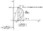
複素平面でインピーダンスZ0のベクトルの軌跡を表すと図5に示すようになる。
Putting the M 0T 2 = L 0 L T
The coupling coefficient k is inversely proportional to the distance between the exciting coil and the object to be detected.
When k = 1, Z 0 = R 0
When k = 0, Z 0 = R 0 + jωL 0
Z 0 (RT = ∞) = R 0 + jωL 0 + (ω 2 M 0T 2 ) / (∞ + jωL T )
= R 0 + jωL 0
When the locus of the vector of impedance Z 0 is represented in the complex plane, it is as shown in FIG.
図5のZ0ベクトル軌跡は、式(7)で容量成分を省略したため実数部Re−虚数部Im平面の第一象限の軌跡となる。このZ0ベクトル軌跡を利用して被検出体を検出する場合の特徴は、下記1)〜3)となる。
1)検出感度を大きくする=軌跡の円弧を大きくする=L0を大きくする。
2)被検出体が無い状態でZ0が最大。そのため、所定の電流I0を流すための電圧E0が相対的に大きな値が必要となる。
3).被検出体抵抗:RT=0のとき、Z0は最小となり、そのとき最大電流が流れることになる。
The Z 0 vector locus in FIG. 5 is a locus in the first quadrant of the real part Re-imaginary part Im plane because the capacitance component is omitted in Equation (7). The characteristics when the detected object is detected using the Z 0 vector locus are the following 1) to 3).
1) the detection sensitivity is increased = the arc path is increased = increasing the L 0.
2) Z 0 is maximum with no object to be detected. Therefore, a relatively large value is required for the voltage E 0 for flowing the predetermined current I 0 .
3). When the resistance of the object to be detected: R T = 0, Z 0 is minimum, and then the maximum current flows.
また、具体的な回路パラメータを使い計算すると重要な特徴が浮き彫りになる。図6はZ0とRTの関係を示す図である。図6に示す通り、各kでのZ0ベクトル軌跡の同一RTプロットは、直線上にのることが分かる。結合係数kは、センサヘッドと被検出体間の距離に反比例する。しかし、この距離が変化しても同上直線とZ0(Im)軸との角度を計測すれば、被検出体側の二次回路抵抗RTを同定することができることがわかる。被検出体側の膜厚は、被検出体の二次回路抵抗RTに反比例することが分かっているから、センサヘッドと被検出体間の距離変動にロバストな膜厚計測ができることを示している。 In addition, important features are highlighted when calculated using specific circuit parameters. FIG. 6 is a diagram showing the relationship between Z 0 and R T. As shown in FIG. 6, it can be seen that the same RT plot of the Z 0 vector locus at each k is on a straight line. The coupling coefficient k is inversely proportional to the distance between the sensor head and the detected object. However, it can be seen that the secondary circuit resistance RT on the detected object side can be identified by measuring the angle between the straight line and the Z 0 (Im) axis even if this distance changes. Since the film thickness on the detected object side is known to be inversely proportional to the secondary circuit resistance RT of the detected object, this indicates that the film thickness can be measured robust to variations in the distance between the sensor head and the detected object. .
続いて、上記特徴2)、3)の対策として、励磁周波数での初期励磁源インピーダンスZ0を小さくするためにLCR直列共振回路特性を利用する場合がある。この場合には、式(7)に容量成分項:−j(1/ωC)を加えることになる。
Z0=R0+jωL0+(ω2M0T 2)/(RT+jωLT)−j1/ωC
=R0+〔(ω2M0T 2)/(RT 2+ω2LT 2)〕RT
+j〔ωL0−ω{(ω2M0T 2)/(RT 2+ω2LT 2)}LT−1/ωC〕
・・・(8)
Z0(RT=0)=R0+0+j〔ωL0−ω(M0T 2)/(LT)〕−1/ωC〕
M0T=(LTL0)1/2kとおくと、
Z0=R0+j〔ωL0−ωL0k2−1/ωC〕
k=1のとき、
Z0=R0−j1/ωC
となる。ここで注目する点は複素(Re−Im)平面の第四象限ベクトルの成分であり、Cが小さいほど軌跡円弧大となることである。
Subsequently, as a countermeasure for the above features 2) and 3), there is a case where the LCR series resonance circuit characteristic is used to reduce the initial excitation source impedance Z 0 at the excitation frequency. In this case, the capacitive component term: -j (1 / ωC) is added to the equation (7).
Z 0 = R 0 + jωL 0 + (ω 2 M 0T 2 ) / (R T + jωL T ) −j1 / ωC
= R 0 + [(ω 2 M 0T 2) / (
+ J [ωL 0 -ω {(ω 2 M 0T 2) / (
... (8)
Z 0 (RT = 0) = R 0 + 0 + j [ωL 0 −ω (M 0T 2 ) / (L T )] − 1 / ωC]
If M 0T = (L T L 0 ) 1/2 k,
Z 0 = R 0 + j [ωL 0 −ωL 0 k 2 −1 / ωC]
When k = 1
Z 0 = R 0 −j1 / ωC
It becomes. The point of interest here is the component of the fourth quadrant vector in the complex (Re-Im) plane, and the smaller the C, the larger the locus arc.
続いて、RT=∞では、
Z0(RT=∞)=R0+0+j〔ωL0−0−1/ωC〕
=R0+j(ωL0−1/ωC)
ここで注目する点は、Z0(RT=∞)はkに依存しないことである。ω=1/(L0C)1/2より、
C=1/ω2L0
Z0=R0+j(ωL0−ω2L0/ω)=R0
となる。このベクトル軌跡を図7に示す。ここで注目する点は、図7に示すように、全てのZ0はZ0=R0に収束し、初期状態のインピーダンスZ0は最小値となることである。
Subsequently, when R T = ∞,
Z 0 (RT = ∞) = R 0 + 0 + j [ωL 0 −0−1 / ωC]
= R 0 + j (ωL 0 −1 / ωC)
The point to be noted here is that Z 0 (RT = ∞) does not depend on k. From ω = 1 / (L 0 C) 1/2 ,
C = 1 / ω 2 L 0
Z 0 = R 0 + j (ωL 0 −ω 2 L 0 / ω) = R 0
It becomes. This vector locus is shown in FIG. The point to be noted here is that, as shown in FIG. 7, all Z 0 converge to Z 0 = R 0, and the impedance Z 0 in the initial state becomes the minimum value.
上記Z0のベクトル軌跡を利用して被検出体を検出する場合の特徴は、下記1)、2)となる。
1)検出感度を大きくする=軌跡の円弧を大きくする=Cを小さくする。言い換えれば、L0を大きくすることを意味している。
2)被検出体抵抗:RT=∞のとき、つまり初期状態(被検出体無しの状態)でZ0最小となり、そのとき最大電流が流れることになる。
The characteristics when the detected object is detected by using the vector locus of Z 0 are the following 1) and 2).
1) Increase the detection sensitivity = Increase the arc of the locus = Reduce C. In other words, it means increasing L 0 .
2) Resistance to be detected: When R T = ∞, that is, Z 0 is minimum in the initial state (state without detection object), and then the maximum current flows.
上記インピーダンスZ0の変化を何で検出するかによって検出方法、呼び方に種類がある。その一つが図4に示す構成の渦電流センサである。図4に示す構成の渦電流センサを図8を用いて整理する。励磁コイル11の両側(図では上下側)に第1検出コイル12と第2検出コイル13が配置されている。第1検出コイル12に誘起される誘起電圧V1=−N1(Δφ/Δt)、第2検出コイル13に誘起される電圧V2=−N2(Δφ/Δt)とし、電位の基準(接地側)を第1検出コイル12はコイルの下側、第2検出コイル13ではコイルの上側としている。第1検出コイル12の誘起電圧V1と第2検出コイル13の誘起電圧V2は反対にしている。よって、誘起電圧V1と誘起電圧V2の電位変位を観察すると定常状態からのΔφ分を検出できる。
There are various types of detection methods and designations depending on how the change in the impedance Z 0 is detected. One of them is an eddy current sensor having the configuration shown in FIG. The eddy current sensor having the configuration shown in FIG. 4 is organized with reference to FIG. A
一定電圧E0で励磁コイル11を駆動した場合の励磁電流I0は、インピーダンスZ0の変化により変化する。励磁電流I0により発生する磁束φは、励磁電流I0に比例する。磁束φは、周波数ωの交番磁束であるから、第1検出コイル12、第2検出コイル13の両端には、電磁誘導現象により誘起電圧V1、V2が発生する。初期状態(RT=∞、或いは被検出体が無い)での起電力成分をキャンセルさせ、初期状態からの変化を観測しやすくするため第1検出コイル12と第2検出コイル13の2つの検出コイルを用いている。
When the
次に、上記第1検出コイル12と第2検出コイル13の影響を説明するために、図4の第1検出コイル12と第2検出コイル13、円筒状センサヘッド15の周囲を筒状の周囲部材で囲まれた場合の成分をモデルに置き換え、式(8)に追加する。
Z0=R0+jωL0
+(ω2M0T 2)/(RT+jωLT)
+(ω2M01 2)/(R1+jωL1)
+(ω2M02 2)/(R2+jωL2)
+(ω2M0m 2)/(Rm+jωLm)−j1/ωC・・・・・・・・(9)
Next, in order to explain the influence of the
Z 0 = R 0 + jωL 0
+ (Ω 2 M 0T 2 ) / (R T + jωL T )
+ (Ω 2 M 01 2 ) / (R 1 + jωL 1 )
+ (Ω 2 M 02 2 ) / (R 2 + jωL 2 )
+ (Ω 2 M 0m 2 ) / (R m + jωL m ) −j1 / ωC (9)
ここで、(ω2M0T 2)/(RT+jωLT)は被検出体成分で、(ω2M01 2)/(R1+jωL1)は第1検出コイル12の成分、(ω2M02 2)/(R2+jωL2)は第2検出コイル13の成分、(ω2M0m 2)/(Rm+jωLm)は周囲部材の成分である。そしてそれぞれ、
(ω2M0T 2)/(RT+jωLT)=(ω2M0T 2)(RT−jωLT)/(RT 2+ω2LT 2)
(ω2M01 2)/(R1+jωL1)=(ω2M01 2)(R1−jωL1)/(R1 2+ω2L1 2)
(ω2M02 2)/(R2+jωL2)=(ω2M02 2)(R2−jωL2)/(R2 2+ω2L2 2)
(ω2M0m 2)/(Rm+jωLm)=(ω2M0m 2)(Rm−jωLm)/(Rm 2+ω2Lm 2)
となる。
Here, (ω 2 M 0T 2 ) / (R T + jωL T ) is a component to be detected, (ω 2 M 01 2 ) / (R 1 + jωL 1 ) is a component of the
(Ω 2 M 0T 2) / (R T + jωL T) = (ω 2 M 0T 2) (R T -jωL T) / (
(Ω 2 M 01 2 ) / (R 1 + jωL 1 ) = (ω 2 M 01 2 ) (R 1 −jωL 1 ) / (R 1 2 + ω 2 L 1 2 )
(Ω 2 M 02 2 ) / (R 2 + jωL 2 ) = (ω 2 M 02 2 ) (R 2 −jωL 2 ) / (R 2 2 + ω 2 L 2 2 )
(Ω 2 M 0m 2 ) / (R m + jωL m ) = (ω 2 M 0m 2 ) (R m −jωL m ) / (R m 2 + ω 2 L m 2 )
It becomes.
従って、式(9)の実数部Re、虚数部Imはそれぞれ、
Re) (ω2M0T 2RT)/(RT 2+ω2LT 2)
+(ω2M01 2R1)/(R1 2+ω2L1 2)
+(ω2M02 2R2)/(R2 2+ω2L2 2)
+(ω2M0m 2Rm)/(Rm 2+ω2Lm 2)+R0
Im) −jω〔(ω2M0T 2LT)/(RT 2+ω2LT 2)
+(ω2M01 2L1)/(R1 2+ω2L1 2)
+(ω2M02 2L2)/(R2 2+ω2L2 2)
+(ω2M0m 2Lm)/(Rm 2+ω2Lm 2)〕−j1/ωC+jωL0
となる。
Therefore, the real part Re and the imaginary part Im in the equation (9) are respectively
Re) (ω 2 M 0T 2 R T ) / (R T 2 + ω 2 L T 2 )
+ (Ω 2 M 01 2 R 1 ) / (R 1 2 + ω 2 L 1 2 )
+ (Ω 2 M 02 2 R 2 ) / (R 2 2 + ω 2 L 2 2 )
+ (Ω 2 M 0m 2 R m ) / (R m 2 + ω 2 L m 2 ) + R 0
Im) -jω [(ω 2 M 0T 2 L T ) / (
+ (Ω 2 M 01 2 L 1 ) / (R 1 2 + ω 2 L 1 2 )
+ (Ω 2 M 02 2 L 2 ) / (R 2 2 + ω 2 L 2 2 )
+ (Ω 2 M 0m 2 L m ) / (R m 2 + ω 2 L m 2 )] − j1 / ωC + jωL 0
It becomes.
Z0(RT=0)=R0+0+〔(ω2M01 2)/(R1 2+ω2L1 2)〕R1
+〔(ω2M02 2)/(R2 2+ω2L2 2)〕R2
+〔(ω2M0m 2)/(Rm 2+ω2Lm 2)〕Rm
+j〔ωL0−ω{(ω2M0T 2)/(0+ω2LT 2)}LT
−ω{(ω2M01 2)/(R1 2+ω2L1 2)}L1
−ω{(ω2M02 2)/(R2 2+ω2L2 2)}L2
−ω{(ω2M0m 2)/(Rm 2+ω2Lm 2)}Lm−1/(ωC)〕
Z 0 (RT = 0) = R 0 +0 + [(ω 2 M 01 2 ) / (R 1 2 + ω 2 L 1 2 )] R 1
+ [((Ω 2 M 02 2 ) / (R 2 2 + ω 2 L 2 2 )] R 2
+ [((Ω 2 M 0m 2 ) / (R m 2 + ω 2 L m 2 )] R m
+ J [ωL 0 -ω {(ω 2 M 0T 2) / (0 +
−ω {(ω 2 M 01 2 ) / (R 1 2 + ω 2 L 1 2 )} L 1
−ω {(ω 2 M 02 2 ) / (R 2 2 + ω 2 L 2 2 )} L 2
−ω {(ω 2 M 0m 2 ) / (R m 2 + ω 2 L m 2 )} L m −1 / (ωC)]
ここでRm≒∞(周囲部材の材質を絶縁体)とする。Cは第1検出コイル12、第2検出コイル13を含んだ励磁源から見た成分(RT=∞)とωより設定するから、
L=Z0(Im)/ω=L0−〔(ω2M01 2)/(R1 2+ω2L1 2)〕L1
−〔(ω2M02 2)/(R2 2+ω2L2 2)〕L2
C=1/(ω2L)より、1/ωC=ωL
M0Tは第1検出コイル12、第2検出コイル13を含んだLとLTとの相互インダクタンスとし、M0T=(LLT)1/2kとおくと、
Here, R m ≈∞ (the material of the surrounding member is an insulator). C is set from the component (R T = ∞) viewed from the excitation source including the
L = Z 0 (Im) / ω = L 0 − [(ω 2 M 01 2 ) / (R 1 2 + ω 2 L 1 2 )] L 1
− [(Ω 2 M 02 2 ) / (R 2 2 + ω 2 L 2 2 )] L 2
From C = 1 / (ω 2 L), 1 / ωC = ωL
M 0T is a mutual inductance between L and L T including the
Z0=R0+0+〔(ω2M01 2)/(R1 2+ω2L1 2)〕R1
+〔(ω2M02 2)/(R2 2+ω2L2 2)〕R2+0
+j〔ωL0−ω{(ω2LLTk2)/(0+ω2LT 2)}LT
−ω{(ω2M01 2)/(R1 2+ω2L1 2)}L1
−ω{(ω2M02 2)/(R2 2+ω2L2 2)}L2−ωL〕
Z0(Im)成分は、−jωLk2=−jω〔−L0+{(ω2M01 2)/(R1 2+ω2L1 2)}L1+{(ω2M02 2)/(R2 2+ω2L2 2)}L2〕k2
k=1のとき、
Z0=R0+〔(ω2M01 2)/(R1 2+ω2L1 2)〕R1
+〔(ω2M02 2)/(R2 2+ω2L2 2)〕R2
−jω〔−L0+{(ω2M01 2)/(R1 2+ω2L1 2)}L1+{(ω2M02 2)/
(R2 2+ω2L2 2)}L2〕
ここで注目すべき点は複素(Re−Im)平面の第四象限ベクトルの成分であり、そのベクトルの絶対値(大きさ)が検出コイルの影響分大きくなることである。
Z 0 = R 0 +0 + [(ω 2 M 01 2 ) / (R 1 2 + ω 2 L 1 2 )] R 1
+ [(Ω 2 M 02 2 ) / (R 2 2 + ω 2 L 2 2 )] R 2 +0
+ J [ωL 0 -ω {(ω 2 LL T k 2) / (0 +
−ω {(ω 2 M 01 2 ) / (R 1 2 + ω 2 L 1 2 )} L 1
−ω {(ω 2 M 02 2 ) / (R 2 2 + ω 2 L 2 2 )} L 2 −ωL]
The Z 0 (I m ) component is −jωLk 2 = −jω [−L 0 + {(ω 2 M 01 2 ) / (R 1 2 + ω 2 L 1 2 )} L 1 + {(ω 2 M 02 2 ) / (R 2 2 + ω 2 L 2 2 )} L 2 ] k 2
When k = 1
Z 0 = R 0 + [(ω 2 M 01 2 ) / (R 1 2 + ω 2 L 1 2 )] R 1
+ [((Ω 2 M 02 2 ) / (R 2 2 + ω 2 L 2 2 )] R 2
−jω [−L 0 + {(ω 2 M 01 2 ) / (R 1 2 + ω 2 L 1 2 )} L 1 + {(ω 2 M 02 2 ) /
(R 2 2 + ω 2 L 2 2 )} L 2 ]
What should be noted here is the component of the fourth quadrant vector in the complex (Re-Im) plane, and the absolute value (magnitude) of the vector is increased by the influence of the detection coil.
Z0(RT=∞)=R0+0+〔(ω2M01 2)/(R1 2+ω2L1 2)〕R1
+〔(ω2M02 2)/(R2 2+ω2L2 2)〕R2
+〔(ω2M0m 2)/(Rm 2+ω2Lm 2)〕Rm
+j〔ωL0−0−ω{(ω2M01 2)/(R1 2+ω2L1 2)}L1
−ω{(ω2M02 2)/(R2 2+ω2L2 2)}L2
−ω{(ω2M0m 2)/(Rm 2+ω2Lm 2)}Lm−1/(ωC)〕
Rm≒∞(周囲材質が絶縁体)、Cは第1検出コイル12、第2検出コイル13を含んだL成分とωより設定するから、
ω=1/(LC)1/2
L=Z0(Im)/ω
=〔ωL0−ω{(ω2M01 2)/(R1 2+ω2L1 2)}L1
−ω{(ω2M02 2)/(R2 2+ω2L2 2)}L2〕/ω
=L0−{(ω2M01 2)/(R1 2+ω2L1 2)}L1
−{(ω2M02 2)/(R2 2+ω2L2 2)}L2
よって、C=1/(ω2L)より、1/(ωC)=ωL
Z 0 (RT = ∞) = R 0 +0 + [(ω 2 M 01 2 ) / (R 1 2 + ω 2 L 1 2 )] R 1
+ [((Ω 2 M 02 2 ) / (R 2 2 + ω 2 L 2 2 )] R 2
+ [((Ω 2 M 0m 2 ) / (R m 2 + ω 2 L m 2 )] R m
+ J [ωL 0 −0−ω {(ω 2 M 01 2 ) / (R 1 2 + ω 2 L 1 2 )} L 1
−ω {(ω 2 M 02 2 ) / (R 2 2 + ω 2 L 2 2 )} L 2
−ω {(ω 2 M 0m 2 ) / (R m 2 + ω 2 L m 2 )} L m −1 / (ωC)]
R m ≈∞ (the surrounding material is an insulator), and C is set from the L component including the
ω = 1 / (LC) 1/2
L = Z 0 (I m ) / ω
= [ΩL 0 −ω {(ω 2 M 01 2 ) / (R 1 2 + ω 2 L 1 2 )} L 1
−ω {(ω 2 M 02 2 ) / (R 2 2 + ω 2 L 2 2 )} L 2 ] / ω
= L 0 − {(ω 2 M 01 2 ) / (R 1 2 + ω 2 L 1 2 )} L 1
− {(Ω 2 M 02 2 ) / (R 2 2 + ω 2 L 2 2 )} L 2
Therefore, from C = 1 / (ω 2 L), 1 / (ωC) = ωL
Z0=Re成分+jω〔L0−{(ω2M01 2)/(R1 2+ω2L1 2)}L1
−{(ω2M02 2)/(R2 2+ω2L2 2)}L2−L〕
ここで、〔L0−{(ω2M01 2)/(R1 2+ω2L1 2)}L1−{(ω2M02 2)/(R2 2+ω2L2 2)}L2−L〕=0、よってRT=∞で、Z0=Re成分のみ
=R0+〔(ω2M01 2)/(R1 2+ω2L1 2)〕R1
+〔(ω2M02 2)/(R2 2+ω2L2 2)〕R2
このベクトル軌跡を図9に示す。ここで注目する点は、図9に示すように、Z0ベクトルの絶対値(大きさ)に対して変化分の割合が小さくなったことである。
Z 0 = Re component + jω [L 0 − {(ω 2 M 01 2 ) / (R 1 2 + ω 2 L 1 2 )} L 1
− {(Ω 2 M 02 2 ) / (R 2 2 + ω 2 L 2 2 )} L 2 −L]
Here, [L 0 − {(ω 2 M 01 2 ) / (R 1 2 + ω 2 L 1 2 )} L 1 − {(ω 2 M 02 2 ) / (R 2 2 + ω 2 L 2 2 )} L 2 −L] = 0, and therefore R T = ∞, Z 0 = Re component only = R 0 + [(ω 2 M 01 2 ) / (R 1 2 + ω 2 L 1 2 )] R 1
+ [((Ω 2 M 02 2 ) / (R 2 2 + ω 2 L 2 2 )] R 2
This vector locus is shown in FIG. The point to be noted here is that, as shown in FIG. 9, the ratio of the change is small with respect to the absolute value (magnitude) of the Z 0 vector.
以上より、このZ0ベクトル軌跡を利用して被検出体を検出する場合の特徴は、下記1)〜4)となる。
1)検出感度を大きくするには、軌跡の円弧を大きくする。即ちL0を大きくする。
2)第1検出コイル12、第2検出コイル13の影響により初期状態のZ0は大きくなる。即ち、励磁電流I0が低下し、磁束φが低下する。
3)第1検出コイル12、第2検出コイル13の影響によりZ0の変化分が少なくなる。即ち、被検出体の膜厚変化によるZ0の変化が低下する。これは検出感度が低下することを意味している。
4)検出コイルに並列接続する抵抗値は、大きいほどZ0への影響が小さくなる。
From the above, the features when detecting the detected object using this Z 0 vector locus are the following 1) to 4).
1) To increase the detection sensitivity, the arc of the locus is increased. That is, L 0 is increased.
2) Z 0 in the initial state increases due to the influence of the
3) Due to the influence of the
4) The larger the resistance value connected in parallel with the detection coil, the smaller the influence on Z 0 .
なお、並列抵抗値の値は、被検出体の膜厚測定レンジ上限抵抗値相当以上にするとよい。ただし、この抵抗値は、図4の可変抵抗器VR2の調整で最終的に決まる。この調整とは、図8の誘起電圧V1、V2の位相調整である。そのため、並列抵抗値とコイルの並列回路の特性根:ωn=R/L[rad/sec]が励磁周波数ωのω/10〜10ωの範囲が良い。 Note that the value of the parallel resistance value may be equal to or greater than the film thickness measurement range upper limit resistance value of the object to be detected. However, this resistance value is finally determined by adjusting the variable resistor VR2 in FIG. This adjustment is a phase adjustment of the induced voltages V1 and V2 in FIG. Therefore, the characteristic root of the parallel resistance value and the parallel circuit of the coil: ωn = R / L [rad / sec] is preferably in the range of ω / 10 to 10Ω of the excitation frequency ω.
一定電圧E0で励磁コイル11を駆動した場合の励磁電流I0は、インピーダンスZ0の変化により変化する。励磁電流I0により発生する磁束φは、該励磁電流I0に比例する。磁束φは、周波数ωの交番磁束であるから第1検出コイル12、第2検出コイル13の両端には、電磁誘導現象により誘導起電圧が発生する。この誘起電圧Vは、V=−N(Δφ/Δt)(N:コイル巻数)であるから、誘起電圧Vを検出することで磁束φの周波数ωでの変動成分を観測でき、よってインピーダンスZ0の変化を観測していることになる。誘起電圧Vを検出した後の詳しい信号処理は、本願の要旨ではないのでその説明は省略する。(例えば特許文献1参照)
When the
上記に記載する方法で被検出体の膜厚や研磨プロセスの終点検知などを達成している。基本原理に電磁誘導現象を利用しているから、上記のように周囲の物体が導電体であるとその影響を大きく受ける。Z0ベクトル軌跡に対する円筒状のセンサヘッド15の周囲構造物が比較的抵抗値の低い材質で構成されている場合の影響について説明する。式(9)の周囲材質の項を活かして整理すると、
・被検出体との結合係数:k=1
・Cは第1検出コイル12及び第2検出コイル13を含んだ励磁源からみたL成分(RT=∞)とωより設定する。但し、このL成分には、周囲構造物の材質の影響を含まず、周囲の構造物を絶縁体として設定する。
・M0Tは、第1検出コイル12及び第2検出コイル13と抵抗値の下がった周囲導体のLmを含んだL’とLTとの相互インダクタンスとし、M0T=(L’LTk)1/2とおくと、
L’=Z0(Im)/ω
=〔ωL0−ω{(ω2M01 2)/(R1 2+ω2L1 2)}L1
−ω{(ω2M02 2)/(R2 2+ω2L2 2)}L2
−ω{(ω2M02 2)/(Rm 2+ω2Lm 2)}Lm〕/ω
=L0−{(ω2M01 2)/(R1 2+ω2L1 2)}L1
−{(ω2M02 2)/(R2 2+ω2L2 2)}L2
−{(ω2M02 2)/(Rm 2+ω2Lm 2)}Lm
Z0(RT=0)=R0+〔(ω2M01 2)/(R1 2+ω2L1 2)〕R1
+〔(ω2M02 2)/(R2 2+ω2L2 2)〕R2
+〔(ω2M0m 2)/(Rm 2+ω2Lm 2)〕Rm
+j〔ωL0−ωL’−ω{(ω2M01 2)/(R1 2+ω2L1 2)}L1
−ω{(ω2M02 2)/(R2 2+ω2L2 2)}L2
−ω{(ω2M0m 2)/(Rm 2+ω2Lm 2)}Lm−ωL〕
The method described above achieves the film thickness of the object to be detected and the end point detection of the polishing process. Since the electromagnetic induction phenomenon is used for the basic principle, the influence is greatly affected if the surrounding object is a conductor as described above. The influence when the surrounding structure of the
-Coupling coefficient with detected object: k = 1
C is set from the L component (R T = ∞) viewed from the excitation source including the
M 0T is a mutual inductance between L ′ and L T including L m of the
L ′ = Z 0 (I m ) / ω
= [ΩL 0 −ω {(ω 2 M 01 2 ) / (R 1 2 + ω 2 L 1 2 )} L 1
−ω {(ω 2 M 02 2 ) / (R 2 2 + ω 2 L 2 2 )} L 2
−ω {(ω 2 M 02 2 ) / (R m 2 + ω 2 L m 2 )} L m ] / ω
= L 0 − {(ω 2 M 01 2 ) / (R 1 2 + ω 2 L 1 2 )} L 1
− {(Ω 2 M 02 2 ) / (R 2 2 + ω 2 L 2 2 )} L 2
− {(Ω 2 M 02 2 ) / (R m 2 + ω 2 L m 2 )} L m
Z 0 (RT = 0) = R 0 + [(ω 2 M 01 2 ) / (R 1 2 + ω 2 L 1 2 )] R 1
+ [((Ω 2 M 02 2 ) / (R 2 2 + ω 2 L 2 2 )] R 2
+ [((Ω 2 M 0m 2 ) / (R m 2 + ω 2 L m 2 )] R m
+ J [ωL 0 −ωL′−ω {(ω 2 M 01 2 ) / (R 1 2 + ω 2 L 1 2 )} L 1
−ω {(ω 2 M 02 2 ) / (R 2 2 + ω 2 L 2 2 )} L 2
−ω {(ω 2 M 0m 2 ) / (R m 2 + ω 2 L m 2 )} L m −ωL]
Z0の虚数(Im)成分Z0(Im)は、L=L0−{(ω2M01 2)/(R1 2+ω2L1 2)}L1−{(ω2M02 2)/(R2 2+ω2L2 2)}L2より、
Z0(Im)=j〔−ωL’−ω{(ω2M0m 2)/(Rm 2+ω2Lm 2)}Lm〕
=−jω〔−L0+{(ω2M01 2)/(R1 2+ω2L1 2)}L1
+{(ω2M02 2)/(R2 2+ω2L2 2)}L2〕
Z0(RT=0)=R0+〔(ω2M01 2)/(R1 2+ω2L1 2)〕R1
+〔(ω2M02 2)/(R2 2+ω2L2 2)〕R2
+〔(ω2M0m 2)/(Rm 2+ω2Lm 2)〕Rm
+jω〔L0−{(ω2M01 2)/(R1 2+ω2L1 2)}L1
−{(ω2M02 2)/(R2 2+ω2L2 2)}L2〕
ここで、注目する点は虚数(Im)成分からLmの項が消えることである。
Z0’(RT=∞)=R0+〔(ω2M01 2)/(R1 2+ω2L1 2)〕R1
+〔(ω2M02 2)/(R2 2+ω2L2 2)〕R2
+〔(ω2M0m 2)/(Rm 2+ω2Lm 2)〕Rm
+j〔−ω{(ω2M0m 2)/(Rm 2+ω2Lm 2)}Lm〕
Imaginary (Im) components Z 0 of the Z 0 (I m) is, L = L 0 - {( ω 2
Z 0 (I m ) = j [−ωL′−ω {(ω 2 M 0m 2 ) / (R m 2 + ω 2 L m 2 )} L m ]
= −jω [−L 0 + {(ω 2 M 01 2 ) / (R 1 2 + ω 2 L 1 2 )} L 1
+ {(Ω 2 M 02 2 ) / (R 2 2 + ω 2 L 2 2 )} L 2 ]
Z 0 (RT = 0) = R 0 + [(ω 2 M 01 2 ) / (R 1 2 + ω 2 L 1 2 )] R 1
+ [((Ω 2 M 02 2 ) / (R 2 2 + ω 2 L 2 2 )] R 2
+ [((Ω 2 M 0m 2 ) / (R m 2 + ω 2 L m 2 )] R m
+ Jω [L 0 − {(ω 2 M 01 2 ) / (R 1 2 + ω 2 L 1 2 )} L 1
− {(Ω 2 M 02 2 ) / (R 2 2 + ω 2 L 2 2 )} L 2 ]
Here, the point to be noted is that the term L m disappears from the imaginary number (Im) component.
Z 0 ′ (RT = ∞) = R 0 + [(ω 2 M 01 2 ) / (R 1 2 + ω 2 L 1 2 )] R 1
+ [((Ω 2 M 02 2 ) / (R 2 2 + ω 2 L 2 2 )] R 2
+ [((Ω 2 M 0m 2 ) / (R m 2 + ω 2 L m 2 )] R m
+ J [−ω {(ω 2 M 0m 2 ) / (R m 2 + ω 2 L m 2 )} L m ]
このベクトル軌跡を図10に示す。このように、センサヘッド周囲の材質抵抗が下がり、誘導電流が流れる経路を有するとZ0ベクトルは、大きさは増加し、変化が減少(減衰)することが説明できる。 This vector locus is shown in FIG. Thus, it can be explained that the Z 0 vector increases in magnitude and decreases (attenuates) when the material resistance around the sensor head decreases and the induced current flows.
良導体でも薄膜化が進むと、その材質内での電子の平均自由工程と膜厚とが近づいてくると抵抗率が上昇する。そのため抵抗率の高い被検出体を検知するために、励磁周波数ωを高くする等の感度向上のため対策が採られる。その結果、周囲構造物の材質の影響を無視できなくなることがある。具体的なパラメータを使い計算した結果を参考例として図11に示す。ここでは、励磁周波数ω=29MHz、周囲材質による電気回路抵抗:Rm=IGΩと1kΩの例を示す。 As the thinning of a good conductor progresses, the resistivity increases as the mean free path of electrons within the material approaches the film thickness. Therefore, in order to detect a detection object having a high resistivity, measures are taken to improve sensitivity, such as increasing the excitation frequency ω. As a result, the influence of the material of surrounding structures may not be negligible. FIG. 11 shows a result of calculation using specific parameters as a reference example. Here, an example in which the excitation frequency ω = 29 MHz and the electric circuit resistance due to the surrounding material: Rm = IGΩ and 1 kΩ is shown.
上記のように、渦電流センサの検出感度を向上させる対策の効果を引き出すには、周囲物体の影響を削減する方策を平行して実施する必要がある。本願発明では、比較的高い固有抵抗材質や良導体薄膜の終点検知や膜厚検出の性能向上のために検出感度向上とロバスト性向上を併せて持った渦電流センサを提供する。そのために、励磁コイルや検出コイルの周辺での渦電流(二次電流)発生を防止する磁気回路構造を備えた渦電流センサを提供する。磁気回路を工夫することで渦電流センサの周囲材質が導体であっても発生する誘導起電圧を全体として打ち消すようにする。そのため、周囲材質に二次電流が流れない構造とすることができる。よって、式(9)のRmを∞相当にすることで、周囲材質の影響を削減(理想的には消去)することができる。 As described above, in order to extract the effect of measures for improving the detection sensitivity of the eddy current sensor, it is necessary to implement measures in parallel to reduce the influence of surrounding objects. The present invention provides an eddy current sensor having both detection sensitivity improvement and robustness improvement in order to improve the performance of end point detection and film thickness detection of a relatively high specific resistance material and good conductor thin film. For this purpose, an eddy current sensor having a magnetic circuit structure for preventing the generation of eddy current (secondary current) around an excitation coil and a detection coil is provided. By devising the magnetic circuit, the induced electromotive voltage generated even if the surrounding material of the eddy current sensor is a conductor is canceled out as a whole. Therefore, a structure in which a secondary current does not flow in the surrounding material can be obtained. Therefore, the influence of surrounding materials can be reduced (ideally erased) by setting Rm in Equation (9) to be equivalent to ∞.
なお、上述の励磁回路のLCR直列共振回路特性を利用するためのCの設定と記述したが、Cの値は、100pF以下のレベルである。そのため、実際の回路調整では、配線やコイルなどの必要構造物による容量成分(C)を極力抑える工夫をし合わせ込みすることが多い。(配線とGND距離や配線間距離、コイルの巻き方など) In addition, although it described as the setting of C for utilizing the LCR series resonance circuit characteristic of the above-mentioned excitation circuit, the value of C is a level of 100 pF or less. For this reason, in actual circuit adjustment, there are many cases in which a device that suppresses the capacitance component (C) due to necessary structures such as wiring and coils as much as possible is combined. (Wiring and GND distance, distance between wiring, coil winding method, etc.)
図12は本発明に係る渦電流センサの概略構成を示す。本渦電流センサ20は円環状の励磁コイル21、検出コイル22、23をそれぞれ2個以上(ここではA(左)側とB(右)側の2個)組合せた構成としている。24は励磁コイル21、検出コイル22、23を埋め込んだセンサヘッドであり、該センサヘッド24はプラスチック、セラミック等の絶縁体で構成されている。励磁コイル21をセンサヘッド24の上下方向所定位置に配置し、該励磁コイル21を挟んで検出コイル22、23を上下に配置して構成している。検出コイル22、23の一方の検出コイル(ここでは検出コイル23)を定常状態の誘導電圧成分をキャンセルするバランスコイルとしている。25は周囲導体である。なお、図12(a)、(b)はそれぞれ本渦電流センサ20の平面、断面を示す。
FIG. 12 shows a schematic configuration of an eddy current sensor according to the present invention. The
上記構成の渦電流センサ20において、A側の励磁コイル21の発生磁界による周囲導体25に誘起される誘起電圧Vaによって流れる電流Iaは、A側の励磁コイル21の周囲を周回するように流れたいが、A側の励磁コイル21とB側の励磁コイル21の間のセンサヘッド24の構成部材が絶縁体であるため、電流Iaは限りなく0に近くなる。また、B側の励磁コイル21の発生磁界による周囲導体25に誘起される誘起電圧Vbによって流れる電流Ibは、B側の励磁コイル21の周囲を周回するように流れたいが、上記のようにセンサヘッド24の構成部材が絶縁体であるため、電流Ibは限りなく0に近くなる。理想的には、A側の励磁コイル21により誘起させる誘起電圧VaとB側の励磁コイル21により誘起される誘起電圧VbはVa=Vbとなる。そのためにはA側の励磁コイル21とB側の励磁コイル21の形状寸法と巻数を同じにする。従って、A側の励磁コイル21とB側の励磁コイル21の周囲を回る周回電流Ia−Ibも0となる。
In the
また、A側の検出コイル22、23、及びB側の検出コイル22、23も上記A側及びB側の励磁コイル21と同じに構成され、励磁と検出の相違のみで誘起電圧及び該誘起電圧によって流れる電流は同じであるので、説明は省略する。 The A side detection coils 22 and 23 and the B side detection coils 22 and 23 are also configured in the same manner as the A side and B side excitation coils 21, and the induced voltage and the induced voltage are determined only by the difference between excitation and detection. Since the currents flowing through are the same, the description thereof is omitted.
図12に示す渦電流センサ20を図13(a)、(b)に書き換え、これをベクトル回路で示すと図14のようになり、更に図15(a)、(b)に示すように2つの回路に書き換えることができる。A側のコイルとB側のコイルは巻き方向が互に反対で直列に接続されている。図14の回路において、L01はA側の励磁コイル21を、L02はB側の励磁コイル21をそれぞれ示す。コイルL01、コイルL02に同方向の電流I0を供給したとき、コイルL01で発生する磁束φ1(磁界H1)とコイルL02で発生する磁束φ2〈磁界H2〉の向きが反対となるため、周囲材質の等価電気回路モデルのインダクタンスLm1、Lm2の両端に発生する誘起電圧Vm1と誘起電圧Vm2は互いに向きが反対となる。Lm1とLm2の結合点aは他に継がるルートがない。そのため誘起電圧Vm1+Vm2による電流は流れない。なお、図13(a)において、26は被検出体を示す。
When the
Im1=Vm1/Zm1=−Nm1(Δφ1/Δt)/(Rm1+Rm2+jωLm1)
φ1=(μA01N01/L01)I0
Im2=Vm2/Zm2=−Nm2(Δφ2/Δt)/(Rm1+Rm2+jωLm2)
φ2=(μA02N02/L02)I0
多数の起電力を含む回路網の電流分布は、各起電力が1つずつ単独に存在したときの電流分布の和に等しいとする重合せの理により、磁束φ1、φ2は大きさが同じで互いに反対向きの磁束分布とすれば、周囲材質の形状で決まるNm1=Nm2の条件を加えて、誘起電圧Vm1とVm2を比較すると、Vm1=−Vm2より、Vm1+Vm2=0であり、電流Im1とIm2の流れる方向は反対、また同様にLm1=Lm2であるから、
Zm1=Zm2
よって、
ΣIm=Im1+Im2=0
となる。
I m1 = V m1 / Z m1 = −N m1 (Δφ 1 / Δt) / (R m1 + R m2 + jωL m1 )
φ 1 = (μA 01 N 01 / L 01 ) I 0
I m2 = V m2 / Z m2 = −N m2 (Δφ 2 / Δt) / (R m1 + R m2 + jωL m2 )
φ 2 = (μA 02 N 02 / L 02 ) I 0
The current distribution of the circuit network including a large number of electromotive forces is equal to the sum of the current distributions when each electromotive force is present alone, so that the magnetic fluxes φ 1 and φ 2 have a magnitude of If the magnetic flux distributions are the same and opposite to each other, the condition of N m1 = N m2 determined by the shape of the surrounding material is added and the induced voltages V m1 and V m2 are compared. From V m1 = −V m2 , V m1 Since + V m2 = 0, the currents I m1 and I m2 flow in opposite directions, and similarly L m1 = L m2 ,
Z m1 = Z m2
Therefore,
ΣI m = I m1 + I m2 = 0
It becomes.
図16は本発明に係る渦電流センサ20’の概略構成例を示す図である。本渦電流センサ20’が図12の渦電流センサ20と異なる点は、本渦電流センサ20’ではセンサコイルを励磁コイル21のみとしている点である。図17は渦電流センサ20’を用いた渦電流センサシステム構成を示す図である。A側の励磁コイル21であるコイルL01、該コイルL01と巻方向が反対のB側の励磁コイル21であるコイルL02を直列に接続し、該直列回路に駆動電源E0から周波数ωの交流励磁電流I0を供給するようにしている。
FIG. 16 is a diagram showing a schematic configuration example of an
渦電流センサ20’の信号処理部60は図17に示すように振幅調整器61、位相調整器62、高周波増幅器63、sin成分を検出するsin検波部とcos成分を検出するcos検波部を備えた検波器64で構成されている。駆動電源E0からA側励磁コイル21、B側励磁コイル21に供給される電流I0を電流センサ65で検出し、該電流センサ65からΔI0/Δt=EI相当信号を高周波増幅器63に入力する。振幅調整期器61及び位相調整器62では初期状態(RT=∞)の出力をできるだけ0にするための信号e0を作成し、位相調整器62から信号e0を高周波増幅器63に入力する。また、検波器64には駆動電源E0から検波用基準信号Sが入力される。高周波増幅器63では、(EI−e0)×G=Eout信号を作成し、検波器64に入力する。検波器64ではEoutの実数Re成分と虚数Im成分を検出し、それぞれ出力する。
As shown in FIG. 17, the
図18(a)、(b)は本発明に係る渦電流センサ20’’の概略構成例を示す図である。本渦電流センサ20’’が図16、図17に示す渦電流センサ20‘と異なる点は、センサコイルとしてA、B側の励磁コイル21、21であるコイルL01、L02の他に検出コイル22、22であるコイルL11、L12を設けている点である。そして図18(c)に示すようにコイルL01とL02を直列、コイルL11とL12を直列に接続している。コイルL11とL12の直列回路に接続された抵抗R1の両端の電圧V1は、
V1=−N1Δφ/Δt≒ΔI0/Δt=EI
となり、図17の信号処理部60と同じ構成の信号処理部60を設けることにより、Eoutの実数Re成分と虚数Im成分を検出することができる。
18 (a) and 18 (b) are diagrams showing a schematic configuration example of an eddy current sensor 20 '' according to the present invention. This
V 1 = −N 1 Δφ / Δt≈ΔI 0 / Δt = E I
Next, by providing the
図19は本発明に係る渦電流センサの概略構成を示す。本渦電流センサ30は、半円環状(D型形状)、即ち、径部と半円弧部で形成された励磁コイル31、検出コイル32、33をそれぞれ2個(ここではA(左)側とB(右)側にそれぞれ2個)を互いに背中合せ、即ち径部と径部を対向させて配置した構成としている。34は励磁コイル31、検出コイル32、33を支持(埋め込んだ)するセンサヘッドであり、該センサヘッド34はプラスチック、セラミック等の絶縁体で構成されている。励磁コイル31をセンサヘッド34の上下方向所定位置に配置し、該励磁コイル31を挟んで検出コイル32、33が上下に配置されている。検出コイル32、33の一方の検出コイル(ここでは検出コイル33)をバランスコイルとしている。35は周囲導体である。このようにA側の励磁コイル31、検出コイル32、33、B側の励磁コイル31、検出コイル32、33の平面形状を半円環状とすることにより、円柱状のセンサヘッド34に配置したとき、無駄なスペースの無いセンサヘッドにすることができる。また、センサヘッド34を円柱状にできるので、センサヘッド34と周囲導体35の間にOリングのシール溝37を設け、Oリング36でシールでき、加工精度を出し易く、良好なシール性能を発揮できる。なお、図19(a)、(b)はそれぞれ本渦電流センサ30の平面、断面を示す。
FIG. 19 shows a schematic configuration of an eddy current sensor according to the present invention. This
A側の励磁コイル31の発生磁界による周囲導体35に誘起される誘起電圧Vaによって流れる電流Iaは、A側の励磁コイル31の周囲を周回するように流したいが、センサヘッド34が絶縁体であるため、電流Iaは限りなく0に近くなる。また、B側の励磁コイル31の発生磁界による周囲導体35に誘起される誘起電圧Vbによって流れる電流Ibは、B側の励磁コイル31の周囲を周回するように流したいが、センサヘッド34が絶縁体であるため、電流Ibは限りなく0に近くなる。理想的には、A側の励磁コイル31により誘起させる誘起電圧VaとB側の励磁コイル31により誘起される誘起電圧VbはVa=Vbである。そのためにはA側の励磁コイル31とB側の励磁コイル31の形状寸法と巻数を同じにする。従って、A側の励磁コイル31とB側の励磁コイル31の周囲を回る周回電流Ia−Ibも0となる。
The current Ia flowing by the induced voltage Va induced in the surrounding
また、A側の検出コイル32、33、及びB側の検出コイル32、33もA側及びB側の励磁コイル31と同じに構成され、励磁と検出の相違のみで同じであるので、説明は省略する。 The A side detection coils 32 and 33 and the B side detection coils 32 and 33 are also configured in the same manner as the A side and B side excitation coils 31 and are the same only in the difference between excitation and detection. Omitted.
図20は本発明に係る渦電流センサの概略構成を示す。本渦電流センサ40は励磁コイル41、検出コイル42、43のいずれもA(左)側とB(右)側の平面形状を8の字形状の一体のコイル、即ちA(左)側とB(右)側の一対のコイルを一体の8の字状コイルに形成している。センサヘッド44のセンサコイル装着部44aは、円柱状のセンサヘッド44の上部を小径部とし、該小径部の中央部に縦溝44bを形成した形状としている。このセンサコイル装着部44aに平面8の字形状の励磁コイル41、検出コイル42、43を下方から上方に検出コイル43、励磁コイル41、検出コイル42の順次装着し、A側とB側を等価な磁気回路としている。センサヘッド44はプラスチック、セラミック等の絶縁体で構成されている。ここでも一方の検出コイル43をバランスコイルとする。なお、図20(a)、(b)はそれぞれ本渦電流センサ40の平面図、断面図、(c)はセンサコイル装着部の斜視図を示す。
FIG. 20 shows a schematic configuration of an eddy current sensor according to the present invention. In the present
図21は本発明に係る渦電流センサの概略構成を示す。本渦電流センサ50は励磁コイル51、検出コイル52、53のいずれもA(左)側とB(右)側の平面を1の平面8の字形状の一体のコイル、即ちA(左)側とB(右)側の一対のコイルを一体の8の字状コイルに形成している。A側とB側が交わる部分の開き角度90°で直交させている。このような平面8の字形状の励磁コイル51、検出コイル52、53はプラスチック、セラミック等の絶縁体で構成されているセンサヘッド54内の上下方向所定の位置に励磁コイル51を配置し、該励磁コイル51を挟んで検出コイル52と検出コイル53を上下に配置している。これによりコイル等価回路定数として容量成分Cを削減している。ここでも一方の検出コイル53をバランスコイルとする。なお、図21の(a)、(b)はそれぞれ本渦電流センサ50の平面、断面を示す。
FIG. 21 shows a schematic configuration of an eddy current sensor according to the present invention. In the present
上記実施例1乃至5に示す構成の渦電流センサを導電膜が形成された基板を研磨する基板研磨装置(CMP装置)の膜厚検出センサとして使用すれば、従来の膜厚センサでは、使用できなかった導電体材料、例えばアルミニウムやステンレスを研磨テーブルに使用できる。よってこれら導電体材料のメリットを活用しながら、研磨対象基板の膜厚検出や研磨終点検知を行うことができる。また、比較的高抵抗の被検出体の膜厚や研磨終点を検知するために、励磁周波数を上げた場合でも、導電体材料で構成された研磨テーブルの影響を無視できるレベルまで下げることができる。 If the eddy current sensor having the structure shown in the first to fifth embodiments is used as a film thickness detection sensor for a substrate polishing apparatus (CMP apparatus) for polishing a substrate on which a conductive film is formed, the conventional film thickness sensor can be used. A conductor material that has not been used, such as aluminum or stainless steel, can be used for the polishing table. Therefore, it is possible to detect the film thickness of the substrate to be polished and to detect the end point of polishing while utilizing the merits of these conductor materials. In addition, in order to detect the film thickness and polishing end point of a relatively high resistance object to be detected, even when the excitation frequency is increased, the influence of the polishing table made of the conductive material can be lowered to a level that can be ignored. .
また、従来の渦電流センサをめっき装置で使用する場合、めっき槽の側壁に絶縁体アダプタを取り付け、渦電流センサの周辺材料の影響を無視できる構造とする必要があった。これに対して、上記実施例1乃至5に示す構成の渦電流センサを用いれば、上記のような絶縁体アダプタは不要となる。また、本願渦電流センサは、電気良導体の中でもその影響を小さくできるので、めっき液内で被めっき体のめっき膜の膜厚や終点の検知を実施することが可能となる。 Further, when a conventional eddy current sensor is used in a plating apparatus, it is necessary to attach an insulator adapter to the side wall of the plating tank so that the influence of the peripheral material of the eddy current sensor can be ignored. On the other hand, if the eddy current sensor having the configuration shown in the first to fifth embodiments is used, the insulator adapter as described above becomes unnecessary. In addition, since the eddy current sensor of the present application can reduce the influence among good electrical conductors, it is possible to detect the film thickness and end point of the plating film of the object to be plated in the plating solution.
なお、従来の渦電流センサでは、磁界を発生する箇所が1つであったが、上記実施例1乃至5に示す構成の渦電流センサでは、隣り合う2つの箇所(一対の励磁コイル)となるため、磁束分布の広がり方に影響がでる。そのため、励磁コイルと被検出体との距離を近づけるなどの対策が必要となる場合もある。 In addition, in the conventional eddy current sensor, there was one place which generates a magnetic field, but in the eddy current sensor having the configuration shown in the first to fifth embodiments, there are two adjacent places (a pair of excitation coils). This affects the way the magnetic flux distribution spreads. For this reason, measures such as reducing the distance between the exciting coil and the detection object may be required.
また、本発明に係る渦電流センサは、被検査体の内部欠陥や内部通電の有無を非接触で検出するのにも利用できる。例えば、3次元実装チップの内部接合状態を検出できる。従来の渦電流センサのコイル形状では、磁束が大きく広がり過ぎて、接合不良が一部あっても必要な検出感度が得られがたい。本発明に係る渦電流センサのコイル形状は、2つのコイルを有するから、磁束密度の高い部分が2つのコイル間に発生する。例えば、図19に示すコイル形状とすれば、A(左)側とB(右)側のコイル間にライン状に磁束が集まり、接合不良部の存在を検知しやすく、且つ、場所の特定もしやすくなる。 The eddy current sensor according to the present invention can also be used for non-contact detection of the internal defect of the object to be inspected and the presence or absence of internal energization. For example, the internal bonding state of the three-dimensional mounting chip can be detected. With the coil shape of the conventional eddy current sensor, the required detection sensitivity is difficult to obtain even if the magnetic flux spreads too much and there is a partial bonding failure. Since the coil shape of the eddy current sensor according to the present invention has two coils, a portion having a high magnetic flux density is generated between the two coils. For example, if the coil shape shown in FIG. 19 is used, magnetic flux gathers between the A (left) side and B (right) side coils so that it is easy to detect the presence of a poorly joined portion, and the location can be specified. It becomes easy.
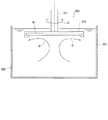
図22は半導体ウエハ等の表面に導電膜が形成された基板を研磨する基板研磨装置において、導電膜の膜厚測定用に本発明に係る渦電流センサを用いた基板研磨装置の要部構成を示す図である。基板研磨装置200は、上面に研磨パッド201が貼り付けられた研磨テーブル202と、基板Wを保持するトップリング210を具備する。この基板研磨装置200において、テーブル支持軸203を介して矢印Aに回転する研磨テーブル202の研磨パッド201上面に、基板板保持面に基板Wを保持し、矢印Bに回転するトップリングの基板Wを当接させ、図示しない研磨液ノズルから研磨パッド201上面に研磨液を供給しながら、基板Wと研磨パッド201の相対運動により、基板Wの表面に形成された導電膜を研磨する。
FIG. 22 shows a substrate polishing apparatus for polishing a substrate having a conductive film formed on the surface of a semiconductor wafer or the like. The configuration of the main part of the substrate polishing apparatus using the eddy current sensor according to the present invention for measuring the film thickness of the conductive film is shown. FIG. The
研磨テーブル202内には、本発明に係る渦電流センサ20が埋め込まれており、該渦電流センサ20には、ロータリジョイント206をテーブル支持軸203を通るケーブル205を介して、駆動電源E0から渦電流センサ20の励磁コイルに周波数ωの交流励磁電流I0を供給し、この交流励磁電流I0を電流センサ65で検出するようになっている。該電流センサ65から図17に示すのと同様、ΔI0/Δt=E1相当信号を高周波増幅器63に入力する。また、振幅調整器61及び位相調整器62では初期状態(RT=∞)の出力をできるだけ0にするための信号e0を作成し、位相調整器62から信号e0を高周波増幅器63に入力する。また、検波器64には駆動電源E0から検波用基準信号Sが入力される。高周波増幅器63では、(EI−e0)×G=Eout信号を作成し、検波器64に入力する。検波器64ではEoutの実数Re成分と虚数Im成分を検出し、それぞれ出力する。
An
上記検波器64からの実数Re成分(X)と虚数Im成分(Y)から、基板Wの導電性膜厚を検出する手法として、特許文献7に開示されているように、θ=Tan-1Y/Xに基づく方法と、抵抗成分とリアクタンス成分との合成インピーダンスに基づく手法と、円弧の長さを測る方法がある。ここでは、基板Wの導電性膜厚を、該導電性膜と渦電流センサ20のギャップGの変化に影響されることなく検出できるθ=Tan-1Y/Xに基づく方法を下記に説明する。
As a technique for detecting the conductive film thickness of the substrate W from the real Re component (X) and the imaginary Im component (Y) from the
図26は駆動電源E0側から見たインピーダンスZの座標の円軌跡を示す図である。縦軸リアクタンス成分Xであり、横軸は抵抗成分Rである。点Cは膜厚が例えば100μm以上と極めて大きい(完全導体とみなせる)場合である。この場合には、駆動電源E0から渦電流センサ20の励磁コイル21に励磁電流I0を通電した場合、導電性膜に流れる渦電流が極めて大きく、励磁コイル21と等価的に並列に接続された抵抗成分Rとリアクタンス成分Xが極めて小さくなる。従って、抵抗成分R及びリアクタンス成分Xが共に小さくなる。
FIG. 26 is a diagram showing a circular locus of the coordinates of the impedance Z viewed from the drive power source E 0 side. The vertical axis represents the reactance component X, and the horizontal axis represents the resistance component R. Point C is the case where the film thickness is extremely large, for example, 100 μm or more (can be regarded as a perfect conductor). In this case, when the excitation current I 0 is supplied from the drive power source E 0 to the
研磨が進行して導電性膜が薄くなると、励磁コイル21の入力端子から見たインピーダンスZは、C点から開始し等価的な抵抗成分Rが増大し、リアクタンス成分Xも増大する。励磁コイル21の入力端子から見たインピーダンスZの抵抗成分Rが最大となる点をBで示す。このとき励磁コイル21の入力端子から見た渦電流損が最大となる。さらに研磨が進行し、導電性膜がより薄くなると、渦電流が減少し、励磁コイル21の入力端子から見た抵抗成分Rは、渦電流損が徐々に減少するから、徐々に小さくなる。そして、導電性膜が全て研磨により除去されると、そこには渦電流損が存在せず、等価的に並列接続された抵抗成分Rは無限大となり、励磁コイル21の抵抗のみが残ることになる。このときのリアクタンス成分Xは、励磁コイル21自体のリアクタンス成分のみである。この状態を、点Aで示す。
As the polishing progresses and the conductive film becomes thinner, the impedance Z seen from the input terminal of the
図27は導電性膜と渦電流センサ20との間のギャップを変化させた場合のインピーダンス座標面における図26の円軌跡の変化を示す図である。渦電流センサ20によるX成分及びY成分の測定結果からは、図に示すように、導電性膜と渦電流センサ20との間のギャップGにかかわらずに、X成分及びY成分の導電性膜の膜厚毎の出力値を直線(r1〜r3)で結ぶと、その直線が交差する点(中心点)Pを取得することができる。この予備測定直線rn(n:1,2,3・・・)はその交点Pを通過するY成分一定の基準線(図27における水平線)Lに対して、導電性膜の膜厚に応じた仰角(挟角)θで傾斜(勾配)する。
FIG. 27 is a diagram showing a change in the circular locus of FIG. 26 on the impedance coordinate plane when the gap between the conductive film and the
このことから、基板Wに形成された導電性膜と渦電流センサ20との間のギャップG(研磨パッド201の厚さ)が変化しても導電性膜のX成分及びY成分の測定結果(出力値)と中心点Pを結ぶ本番測定線rnの基準線Lに対する仰角θを求めれば、予め予備測定済みの導電性膜の膜厚に応じた仰角θの変化傾向などとの相関関係に基づいてその測定対象の導電性膜の膜厚を導出することができる。
From this, even if the gap G (the thickness of the polishing pad 201) between the conductive film formed on the substrate W and the
上記のことは図6の励磁源インピーダンスZ0と被検出体抵抗RTの関係を示す図からも明らかである。即ち、結合係数kは基板Wの導電性膜と渦電流センサ20との間の距離に反比例するが、この距離(係数k)が変化しても同一直線とZ0(Im)軸との角度を計測すれば、被検出体側の二次回路抵抗RTを同定することができるのである。図22の検波器64の出力である実数Re成分と虚数Im成分からθ=tan-1Im/Reを導電性膜の膜厚に対して、予め求めておき、このθと測定対象導電性膜を測定して得られたRe成分とIm成分から求めたθ(θ=tan-1Im/Re)を比較することにより、対象導電性膜の膜厚を検出できる。
The above is also apparent from the diagram showing the relationship between the excitation source impedance Z 0 and the detected object resistance RT in FIG. That is, the coupling coefficient k is inversely proportional to the distance between the conductive film of the substrate W and the
上記のように基板研磨装置200で、研磨中に基板Wの導電性膜厚を高精度で検出することにより、例えばエンドポイント等を精度よく検出し、研磨を終了させることができる。即ち、渦電流センサ20で基板Wの導電性膜の膜厚状況を監視しながら、研磨の進捗を知ることができる。
As described above, by detecting the conductive film thickness of the substrate W with high accuracy during polishing by the
なお、ここでは研磨テーブル202、トップリング210を具備し、導電膜が形成された半導体ウエハを基板Wとして研磨する基板研磨装置200を例に説明したが、本発明に係る渦電流センサは、導電膜が形成された被研磨物の該導電膜を研磨する研磨装置の導電膜厚検出のために広く利用できる。なお、上記例では、図12に示す渦電流センサを用いる例を示した、図13、図16、図18、図19、図20、図21に示す渦電流センサでもよいことは当然である。
Here, the
次に、半導体ウエハ等の基板に導電性めっき膜を形成するめっき装置において、基板に形成される導電性膜の膜厚を検出する膜厚検出センサとして、本発明に係る渦電流センサを用いる例について説明する。図23は基板めっき装置の概略構成例を示す図である。なお、ここでは無電解めっき装置を想定して示すので、電解めっき装置であれば、当然備えてる電極やめっき電流供給電源は図示していない。図示するように、めっき装置300は、めっき槽301を備え、該めっき槽301内にめっき液302を収容している。めっき液302に基板ホルダー310の下面に保持した基板Wを浸漬し、基板Wの表面に銅膜等の導電性膜を形成する。導電膜形成中に基板Wを保持した基板ホルダー310を軸311を中心に矢印Aに示すように回転することにより、ポンプ効果によりめっき液302中に矢印Bに示すような旋回流が発生し、基板Wの表面近傍に新鮮なめっき液が積極的に供給される。これにより、基板Wの表面に効率よく導電性めっき膜が形成される。
Next, in a plating apparatus for forming a conductive plating film on a substrate such as a semiconductor wafer, an example in which the eddy current sensor according to the present invention is used as a film thickness detection sensor for detecting the thickness of the conductive film formed on the substrate. Will be described. FIG. 23 is a diagram illustrating a schematic configuration example of a substrate plating apparatus. Here, since the electroless plating apparatus is assumed and shown, the electrode and the plating current supply power source that are naturally provided are not shown in the case of an electroplating apparatus. As shown in the figure, the
上記構成のめっき装置において、従来の渦電流センサを用いて、基板Wの表面に形成された導電性めっき膜の膜厚を測定するには、図24に示すように、基板Wに対向するめっき槽301の側壁(図では底壁)に非導電性材からなるアダプタ321をOリング322を介在させて気密状態で設け、該アダプタ321の凹部323に渦電流センサヘッド324を挿入設置していた。このように基板Wのめっき面と対向するめっき槽301の側壁に非導電性材からなるアダプタ321を設け、その凹部323に渦電流センサヘッド324を挿入設置した構成では、基板Wのめっき面と渦電流センサヘッド324までの距離Lが大きくなり、渦電流センサの感度が低下する。また、めっき槽301の深さ寸法を小さくすると、基板Wのめっき面とめっき槽301の底面との距離が小さくなり、基板ホルダー310を回転させてもポンプ効果による十分なめっき液302の旋回流が発生せず、基板Wに新鮮なめっき液302を供給できずめっき効率が低下するという問題がある。
In the plating apparatus having the above configuration, in order to measure the film thickness of the conductive plating film formed on the surface of the substrate W using the conventional eddy current sensor, as shown in FIG. An
図25は基板Wの表面に形成された導電性膜の膜厚測定に本発明に係る渦電流センサ20を用いためっき装置の構成例を示す図である。図示するように、基板Wに対向するめっき槽301の側壁(図では底壁)に棒状のセンサホルダー330をOリング331を介在させて気密状態で設け、センサホルダー330の先端部に本発明に係る渦電流センサ20を取り付ける。これにより渦電流センサ20と基板Wのめっき面との距離が小さくなり、渦電流センサ20の感度が向上する。このように渦電流センサ20をめっき液中に浸漬しても、本発明に係る渦電流センサは、センサヘッドの側面に導電体があっても、上記のように影響を受けない渦電流センサであるから、問題がない。
FIG. 25 is a diagram showing a configuration example of a plating apparatus using the
基板Wのめっき面に形成される導電性めっき膜の膜厚は、上記基板研磨装置で説明したと同じ方法で検出できる。上記めっき装置において、めっき処理中に渦電流センサ20で基板Wの表面に形成されるめっき膜の膜厚を監視しながら、めっき処理を継続し、所望の膜厚に達したらめっき終了とすることができる。なお、図示は省略するが電解めっき装置においても、めっき処理中に本発明に係る渦電流センサ20で基板Wの表面に形成されるめっき膜の膜厚を監視しながら、めっき処理を継続し、所望の膜厚に達したらめっき終了とすることができる。
The film thickness of the conductive plating film formed on the plating surface of the substrate W can be detected by the same method as described in the substrate polishing apparatus. In the above plating apparatus, the plating process is continued while monitoring the film thickness of the plating film formed on the surface of the substrate W by the
上記本実施例では、渦電流センサの周囲物体を導体としたが、周囲物体は導体に限らず絶縁体でもよい。また、外乱に対して安定な(ロバストな)検出機能を提供できることに変わりはない。 In the present embodiment, the surrounding object of the eddy current sensor is a conductor, but the surrounding object is not limited to a conductor but may be an insulator. In addition, a detection function that is stable (robust) against disturbance can be provided.
以上、本発明の実施形態例を説明したが、本発明は上記実施形態例に限定されるものではなく、特許請求の範囲、及び明細書と図面に記載された技術的思想の範囲内において種々の変形が可能である。 The embodiments of the present invention have been described above. However, the present invention is not limited to the above-described embodiments, and various modifications can be made within the scope of the technical idea described in the claims and the specification and drawings. Can be modified.
本発明は、導電性膜又は導電性膜が形成された基体の膜厚を渦電流センサが配置されている周囲構造物の材料に影響されることなく、安定して検出できる渦電流センサを提供できる。従って、基板面に形成された導電性膜を研磨する研磨装置や基板面に導電性膜を形成するめっき装置の膜厚検出や研磨終点検知等に広く利用できる。 The present invention provides an eddy current sensor that can stably detect the film thickness of a conductive film or a substrate on which a conductive film is formed without being affected by the material of the surrounding structure in which the eddy current sensor is disposed. it can. Therefore, the present invention can be widely used for film thickness detection, polishing end point detection, and the like of a polishing apparatus that polishes a conductive film formed on a substrate surface and a plating apparatus that forms a conductive film on a substrate surface.
11 励磁コイル
12 第1検出コイル
13 第2検出コイル
14 差電圧検出回路
15 センサヘッド
20 渦電流センサ
21 励磁コイル
22 検出コイル
23 検出コイル
24 センサヘッド
25 周囲導体
26 被検出体
30 渦電流センサ
31 励磁コイル
32 検出コイル
33 検出コイル
34 センサヘッド
35 周囲導体
36 Oリング
37 シール溝
40 渦電流センサ
41 励磁コイル
42 検出コイル
43 検出コイル
44 センサヘッド
45 周囲導体
50 渦電流センサ
51 励磁コイル
52 検出コイル
53 検出コイル
54 センサヘッド
55 周囲導体
50 渦電流センサ
51 励磁コイル
52 検出コイル
53 検出コイル
54 センサヘッド
55 周囲導体
60 信号処理部
61 振幅調整器
62 位相調整器
63 高周波増幅器
64 検波器
65 電流センサ
200 基板研磨装置
201 研磨パッド
202 研磨テーブル
203 テーブル支持軸
205 ケーブル
206 ロータリジョイント
210 トップリング
300 めっき装置
301 めっき槽
302 めっき液
311 軸
321 アダプタ
322 Oリング
323 凹部
324 渦電流センサヘッド
DESCRIPTION OF
DESCRIPTION OF
Claims (11)
前記センサコイルはセンサヘッドに配置されており、
前記センサコイルは左右対称に配置された一対のコイルからなり、
前記一対のコイルの各コイルに通電した際に、前記センサヘッドの一方のコイル周囲を周回する電流が、他方のコイル周囲を周回する電流と絶対値が同じで流れの向きが逆になるように配置し、
前記センサコイルの一対のコイルは、それぞれ各センサコイルの中心軸をコイルの中心軸とする一対の励磁用コイルと一対の検出用コイルを具備することを特徴とする渦電流センサ。 A conductive coil or a sensor coil disposed in the vicinity of the substrate on which the conductive film is formed, and an eddy current is induced in the conductive film by passing an alternating current through the sensor coil; In the eddy current sensor for measuring the film thickness of the conductive film by detecting the induced voltage induced in the sensor coil for the generated magnetic flux change,
The sensor coil is disposed in a sensor head;
The sensor coil consists of a pair of coils arranged symmetrically ,
When energizing each coil of the pair of coils, the current circulating around one coil of the sensor head has the same absolute value as the current circulating around the other coil, and the flow direction is reversed. arrangement and,
The pair of coils of the sensor coil includes a pair of excitation coils and a pair of detection coils each having a central axis of each sensor coil as a central axis of the coil .
前記センサヘッドの所定位置に前記励磁用コイルを配置し、該励磁用コイルの上下に前記検出用コイルを配置し、一方の検出用コイルを他方の検出用コイルの定常状態の誘導電圧を打ち消すバランスコイルとしたことを特徴とする渦電流センサ。 The eddy current sensor according to claim 1 .
The excitation coil is arranged at a predetermined position of the sensor head, the detection coils are arranged above and below the excitation coil, and one detection coil is balanced to cancel the steady-state induced voltage of the other detection coil. An eddy current sensor characterized by a coil.
前記励磁用コイルの一対のコイルは、平面8の字状に形成されたコイルであることを特徴とする渦電流センサ。 The eddy current sensor according to claim 1 or 2 ,
An eddy current sensor, wherein the pair of exciting coils are coils formed in a plane 8 shape.
前記検出用コイルの一対のコイルは、平面8の字状に形成されたことを特徴とする渦電流センサ。 The eddy current sensor according to any one of claims 1 to 3 ,
An eddy current sensor, wherein the pair of coils of the detection coil is formed in a plane 8 shape.
前記平面8の字状に形成されたコイルの交差部の開き角度は90°であることを特徴とする渦電流センサ。 The eddy current sensor according to claim 3 or 4 ,
An eddy current sensor characterized in that an opening angle of an intersection of coils formed in the shape of the plane 8 is 90 °.
前記センサヘッドは絶縁体材料で構成されていることを特徴とする渦電流センサ。 The eddy current sensor according to any one of claims 1 to 5 ,
The eddy current sensor is characterized in that the sensor head is made of an insulating material.
前記基板の導電膜の膜厚を検出する膜厚検出センサとして、請求項1乃至6のいずれか1項に記載の渦電流センサを備えたことを特徴とする研磨装置。 In a polishing apparatus for polishing the conductive film of the substrate on which the conductive film is formed,
A polishing apparatus comprising the eddy current sensor according to claim 1 as a film thickness detection sensor for detecting a film thickness of a conductive film on the substrate.
前記基板の導電膜の膜厚を検出する膜厚検出センサとして、請求項6に記載の渦電流センサを用い、該渦電流センサのセンサヘッドを前記導電材料からなる研磨テーブルに埋め込んで取付けたことを特徴とする研磨装置。The eddy current sensor according to claim 6 is used as a film thickness detection sensor for detecting the film thickness of the conductive film on the substrate, and the sensor head of the eddy current sensor is embedded in a polishing table made of the conductive material. A polishing apparatus characterized by the above.
前記基板に形成される導電膜の膜厚を検出する膜厚検出センサとして、請求項1乃至6のいずれか1項に記載の渦電流センサを備えたことを特徴とするめっき装置。 In a plating apparatus for forming a conductive film on a substrate surface ,
A plating apparatus comprising the eddy current sensor according to claim 1 as a film thickness detection sensor for detecting a film thickness of a conductive film formed on the substrate.
前記膜厚センサとして請求項1乃至5のいずれか1項に記載の渦電流センサを用いたことを特徴とする研磨方法。 In the polishing method of polishing the conductive film while monitoring the film thickness of the conductive film of the substrate on which the conductive film is formed with a film thickness sensor,
A polishing method using the eddy current sensor according to claim 1 as the film thickness sensor.
前記膜厚センサとして請求項1乃至5のいずれか1項に記載の渦電流センサを用いたことを特徴とするめっき方法。 In the plating method for forming the conductive film while monitoring the film thickness of the conductive film formed on the surface of the substrate with a film thickness sensor,
A plating method using the eddy current sensor according to claim 1 as the film thickness sensor.
Priority Applications (1)
| Application Number | Priority Date | Filing Date | Title |
|---|---|---|---|
| JP2009216012A JP5513821B2 (en) | 2009-09-17 | 2009-09-17 | Eddy current sensor, polishing apparatus, plating apparatus, polishing method, plating method |
Applications Claiming Priority (1)
| Application Number | Priority Date | Filing Date | Title |
|---|---|---|---|
| JP2009216012A JP5513821B2 (en) | 2009-09-17 | 2009-09-17 | Eddy current sensor, polishing apparatus, plating apparatus, polishing method, plating method |
Publications (3)
| Publication Number | Publication Date |
|---|---|
| JP2011064590A JP2011064590A (en) | 2011-03-31 |
| JP2011064590A5 JP2011064590A5 (en) | 2012-10-25 |
| JP5513821B2 true JP5513821B2 (en) | 2014-06-04 |
Family
ID=43951000
Family Applications (1)
| Application Number | Title | Priority Date | Filing Date |
|---|---|---|---|
| JP2009216012A Active JP5513821B2 (en) | 2009-09-17 | 2009-09-17 | Eddy current sensor, polishing apparatus, plating apparatus, polishing method, plating method |
Country Status (1)
| Country | Link |
|---|---|
| JP (1) | JP5513821B2 (en) |
Families Citing this family (6)
| Publication number | Priority date | Publication date | Assignee | Title |
|---|---|---|---|---|
| WO2016189999A1 (en) * | 2015-05-22 | 2016-12-01 | 三菱電機株式会社 | Electromagnetic field probe |
| JP6756540B2 (en) | 2016-08-08 | 2020-09-16 | 株式会社荏原製作所 | A storage medium containing a plating device, a control method for the plating device, and a program for causing a computer to execute the control method for the plating device. |
| CN106441068A (en) * | 2016-10-31 | 2017-02-22 | 天津因科新创科技有限公司 | Pulsed eddy-current sensor for wall thickness detection |
| WO2018138868A1 (en) | 2017-01-27 | 2018-08-02 | 三菱電機株式会社 | Electromagnetic field probe |
| WO2022046400A1 (en) * | 2020-08-25 | 2022-03-03 | Corning Incorporated | In-situ deposition thickness monitoring |
| TWI750018B (en) * | 2021-01-25 | 2021-12-11 | 日商荏原製作所股份有限公司 | Coating device and substrate film thickness measurement method |
Family Cites Families (25)
| Publication number | Priority date | Publication date | Assignee | Title |
|---|---|---|---|---|
| JPS5543420A (en) * | 1978-09-25 | 1980-03-27 | Saginomiya Seisakusho Inc | Metallic material examination device |
| JPS60144603A (en) * | 1984-01-07 | 1985-07-31 | Nippon Steel Corp | Continuous measuring method of coating thickness of coated metallic tube |
| JPS61159101A (en) * | 1984-10-19 | 1986-07-18 | コルモーゲン コーポレイション | Position and speed sensor |
| JPS61151402A (en) * | 1984-12-26 | 1986-07-10 | Nippon Kokan Kk <Nkk> | Differential mutual induction type eddy current measuring sensor |
| JPS6290502A (en) * | 1985-06-07 | 1987-04-25 | Nippon Kokan Kk <Nkk> | Differential feedback type eddy current distance measuring apparatus |
| JPH0194201A (en) * | 1987-10-06 | 1989-04-12 | Sumitomo Metal Ind Ltd | Method and apparatus for measuring thickness of molten slag |
| DE69233065D1 (en) * | 1991-06-11 | 2003-06-26 | Newt Holdings Ltd | probe |
| JPH05231809A (en) * | 1992-02-24 | 1993-09-07 | Nippon Denshi Kogyo Kk | Electromotive force type eddy current displacement gauge |
| JPH09152423A (en) * | 1995-12-01 | 1997-06-10 | Daido Steel Co Ltd | Probe coil for eddy current flaw detection |
| US6291992B1 (en) * | 1996-07-12 | 2001-09-18 | Shell Oil Company | Eddy current inspection technique |
| JPH10197493A (en) * | 1997-01-14 | 1998-07-31 | Mitsubishi Heavy Ind Ltd | Eddy-current flow detecting probe |
| JPH11248684A (en) * | 1998-03-03 | 1999-09-17 | Daido Steel Co Ltd | Eddy current test equipment |
| JP2000337809A (en) * | 1999-05-28 | 2000-12-08 | Nippon Steel Corp | Differential type eddy current range finder |
| EP1294534B2 (en) * | 2000-05-19 | 2006-01-25 | Applied Materials Inc | In-situ endpoint detection and process monitoring method and apparatus for chemical mechanical polishing |
| US6593737B2 (en) * | 2000-08-24 | 2003-07-15 | Shell Oil Company | Method for measuring the wall thickness of an electrically conductive object |
| US6570379B2 (en) * | 2000-08-24 | 2003-05-27 | Shell Oil Company | Method for inspecting an object of electrically conducting material |
| US6538435B2 (en) * | 2000-08-24 | 2003-03-25 | Shell Oil Company | Method for detecting an anomaly in an object of electrically conductive material along first and second direction at inspection points |
| JP3587822B2 (en) * | 2001-07-23 | 2004-11-10 | 株式会社荏原製作所 | Eddy current sensor |
| US6894491B2 (en) * | 2002-12-23 | 2005-05-17 | Lam Research Corporation | Method and apparatus for metrological process control implementing complementary sensors |
| JP2005011977A (en) * | 2003-06-18 | 2005-01-13 | Ebara Corp | Device and method for substrate polishing |
| JP4451111B2 (en) * | 2003-10-20 | 2010-04-14 | 株式会社荏原製作所 | Eddy current sensor |
| JP4617677B2 (en) * | 2004-02-04 | 2011-01-26 | Jfeスチール株式会社 | Layer thickness measurement method, system, and program for layer thickness measurement method |
| JP5065614B2 (en) * | 2006-04-14 | 2012-11-07 | 株式会社アルバック | Eddy current film thickness meter |
| FR2900471B1 (en) * | 2006-04-26 | 2008-12-26 | Snecma Sa | MEASUREMENT OF WALL THICKNESS, IN PARTICULAR OF DAWN, BY CURRENTS OF FOUCAULT |
| JP2007298323A (en) * | 2006-04-28 | 2007-11-15 | Non-Destructive Inspection Co Ltd | Thickness loss detection method and device by electromagnetic wave pulse |
-
2009
- 2009-09-17 JP JP2009216012A patent/JP5513821B2/en active Active
Also Published As
| Publication number | Publication date |
|---|---|
| JP2011064590A (en) | 2011-03-31 |
Similar Documents
| Publication | Publication Date | Title |
|---|---|---|
| JP5513821B2 (en) | Eddy current sensor, polishing apparatus, plating apparatus, polishing method, plating method | |
| JP4558014B2 (en) | Eddy current sensor and film thickness measuring method using the eddy current sensor | |
| CN104907920B (en) | Correction method, film thickness retriever and the eddy current sensor of film thickness measuring value | |
| US9128063B2 (en) | Non-contact stress measuring device | |
| JP6033751B2 (en) | Polishing method | |
| JP6437586B2 (en) | Measuring probe for measuring the thickness of a thin layer and method for manufacturing a sensor element of a measuring probe | |
| KR102538858B1 (en) | Calibration method of eddy current sensor | |
| JP6779633B2 (en) | Polishing equipment | |
| JP2007318169A (en) | Method of polishing | |
| BR112014019546B1 (en) | APPARATUS AND METHOD FOR MEASURING MATERIAL PROPERTIES OF A FERROMAGNETIC MATERIAL OBJECT | |
| KR20170027284A (en) | Eddy current sensor | |
| TW201015097A (en) | Device for measuring the direction and/or strength of a magnetic field | |
| TWI227775B (en) | Method and apparatus for metrological process control implementing complementary sensors | |
| TWI729152B (en) | Film thickness measuring device, polishing device, film thickness measuring method, and polishing method | |
| TWI741072B (en) | Polishing apparatus and polishing method | |
| JP6590612B2 (en) | Eddy current sensor | |
| JP6445241B2 (en) | Eddy current sensor | |
| RU2420749C1 (en) | Device for noncontact measurement of specific resistance of semiconductor materials | |
| JP5158680B2 (en) | Prediction method at the end of polishing | |
| JP6445771B2 (en) | Method for correcting film thickness measurement value and film thickness corrector | |
| TW201229525A (en) | Electric power measuring apparatus and method | |
| JP2015078942A (en) | Leakage magnetic flux flaw detector | |
| JP2017050381A (en) | Eddy current sensor |
Legal Events
| Date | Code | Title | Description |
|---|---|---|---|
| A521 | Request for written amendment filed |
Free format text: JAPANESE INTERMEDIATE CODE: A523 Effective date: 20120830 |
|
| A621 | Written request for application examination |
Free format text: JAPANESE INTERMEDIATE CODE: A621 Effective date: 20120830 |
|
| A977 | Report on retrieval |
Free format text: JAPANESE INTERMEDIATE CODE: A971007 Effective date: 20130502 |
|
| A131 | Notification of reasons for refusal |
Free format text: JAPANESE INTERMEDIATE CODE: A131 Effective date: 20130514 |
|
| A521 | Request for written amendment filed |
Free format text: JAPANESE INTERMEDIATE CODE: A523 Effective date: 20130626 |
|
| TRDD | Decision of grant or rejection written | ||
| A01 | Written decision to grant a patent or to grant a registration (utility model) |
Free format text: JAPANESE INTERMEDIATE CODE: A01 Effective date: 20140325 |
|
| A61 | First payment of annual fees (during grant procedure) |
Free format text: JAPANESE INTERMEDIATE CODE: A61 Effective date: 20140328 |
|
| R150 | Certificate of patent or registration of utility model |
Ref document number: 5513821 Country of ref document: JP Free format text: JAPANESE INTERMEDIATE CODE: R150 |
|
| R250 | Receipt of annual fees |
Free format text: JAPANESE INTERMEDIATE CODE: R250 |
|
| R250 | Receipt of annual fees |
Free format text: JAPANESE INTERMEDIATE CODE: R250 |
|
| R250 | Receipt of annual fees |
Free format text: JAPANESE INTERMEDIATE CODE: R250 |
|
| R250 | Receipt of annual fees |
Free format text: JAPANESE INTERMEDIATE CODE: R250 |
|
| R250 | Receipt of annual fees |
Free format text: JAPANESE INTERMEDIATE CODE: R250 |
|
| R250 | Receipt of annual fees |
Free format text: JAPANESE INTERMEDIATE CODE: R250 |
|
| R250 | Receipt of annual fees |
Free format text: JAPANESE INTERMEDIATE CODE: R250 |
|
| R250 | Receipt of annual fees |
Free format text: JAPANESE INTERMEDIATE CODE: R250 |