JP5507457B2 - Method of bypassing inoperable network device and network interface apparatus - Google Patents
Method of bypassing inoperable network device and network interface apparatus Download PDFInfo
- Publication number
- JP5507457B2 JP5507457B2 JP2010518170A JP2010518170A JP5507457B2 JP 5507457 B2 JP5507457 B2 JP 5507457B2 JP 2010518170 A JP2010518170 A JP 2010518170A JP 2010518170 A JP2010518170 A JP 2010518170A JP 5507457 B2 JP5507457 B2 JP 5507457B2
- Authority
- JP
- Japan
- Prior art keywords
- transformer
- network
- video signal
- network device
- coupled
- Prior art date
- Legal status (The legal status is an assumption and is not a legal conclusion. Google has not performed a legal analysis and makes no representation as to the accuracy of the status listed.)
- Active
Links
Images


Classifications
-
- H—ELECTRICITY
- H04—ELECTRIC COMMUNICATION TECHNIQUE
- H04L—TRANSMISSION OF DIGITAL INFORMATION, e.g. TELEGRAPHIC COMMUNICATION
- H04L12/00—Data switching networks
- H04L12/28—Data switching networks characterised by path configuration, e.g. LAN [Local Area Networks] or WAN [Wide Area Networks]
- H04L12/42—Loop networks
- H04L12/437—Ring fault isolation or reconfiguration
Description
本発明は、概して、複数の関連するネットワークデバイスにコンテンツ(例えば、オーディオ及び/又はビデオコンテンツ)を分配可能なネットワーク(例えば、イーサネット(登録商標)ネットワーク)に関し、より具体的に、動作不能の又は故障したネットワークデバイスをバイパス可能なネットワークインターフェース装置に関する。 The present invention relates generally to a network (eg, an Ethernet network) that can distribute content (eg, audio and / or video content) to a plurality of associated network devices, and more specifically, inoperable or The present invention relates to a network interface device capable of bypassing a failed network device.
例えばイーサネット(登録商標)ネットワークのようなネットワークで、1つのネットワークデバイスの不具合は、ネットワーク全体を通る信号のフローに計り知れない影響を及ぼしうる。これは、特に、信号が1つのネットワークデバイスから他のネットワークデバイスへ送られるデイジー・チェーン形式で接続されているネットワークに当てはまる。このようなデイジー・チェーン接続ネットワークは、例えば飛行機及びその他の環境でオーディオ及び/又はビデオ信号を分配するために使用されうる。例えば、デイジー・チェーン接続ネットワークは、システム設計を簡単化し且つ必要とされるケーブルの長さ及び数を最小限とするために、このような環境で使用されうる。 For example, in a network such as an Ethernet network, a failure of one network device can have an immense effect on the flow of signals through the network. This is especially true for networks that are connected in a daisy chain fashion where signals are sent from one network device to another. Such daisy chained networks can be used, for example, to distribute audio and / or video signals in airplanes and other environments. For example, a daisy chain connection network can be used in such an environment to simplify system design and minimize the length and number of cables required.
しかし、デイジー・チェーン接続ネットワークで、デイジー・チェーン接続ライン沿いの1つのネットワークデバイスが機能しなくなる場合に、デイジー・チェーン接続ラインにおいて後段にある残りのネットワークデバイスの全ても、分配されるコンテンツへのアクセスを失う。例えば飛行機のような環境では、このような消失は、全ての乗客を故障したデバイスに残し、その後に、フライト中に分配コンテンツ(例えば、オーディオ及び/又はビデオコンテンツ)へのアクセスを有さない。このアクセス消失は、また、多くの不満な乗客とともに、収入の潜在的な損失をも生み出す可能性がある。 However, in a daisy chain connection network, if one network device along the daisy chain connection line fails, all of the remaining network devices in the daisy chain connection line will also contribute to the distributed content. Losing access. In an environment such as an airplane, such disappearance leaves all passengers on the failed device and subsequently has no access to distribution content (eg, audio and / or video content) during the flight. This loss of access can also create a potential loss of revenue, along with many dissatisfied passengers.
従って、ネットワーク(例えば、イーサネット(登録商標)ネットワーク)で使用され、前述の問題を回避するとともに、動作不能のネットワークデバイスがバイパスされることを可能にするネットワークインターフェース装置が必要とされる。ここで記載される発明は、これらの及び/又は他の関連する問題に対処する。 Accordingly, there is a need for a network interface device that can be used in a network (eg, an Ethernet network) to avoid the aforementioned problems and to allow inoperable network devices to be bypassed. The invention described herein addresses these and / or other related issues.
本発明の態様に従って、ネットワークインターフェース装置が開示される。例となる実施形態に従って、ネットワークインターフェース装置は第1及び第2の変圧器を有する。ネットワーク入力部及びネットワーク出力部は夫々、第1の変圧器の第1の側及び第2の変圧器の第1の側に結合される。ターミナル入力部及びターミナル出力部は夫々、第1の変圧器の第2の側及び第2の変圧器の第2の側に結合される。スイッチアセンブリは、第1及び第2の変圧器の第2の側に結合される。スイッチアセンブリが第1の状態にある場合に、第1の変圧器の第2の側はターミナル出力部に結合され、スイッチアセンブリが第2の状態にある場合に、第1の変圧器の第2の側は、ターミナル出力部をバイパスしながら第2の変圧器の第1の側に結合される。 In accordance with an aspect of the present invention, a network interface device is disclosed. According to an exemplary embodiment, the network interface device has first and second transformers. The network input and the network output are respectively coupled to the first side of the first transformer and the first side of the second transformer. A terminal input and a terminal output are coupled to the second side of the first transformer and the second side of the second transformer, respectively. The switch assembly is coupled to the second side of the first and second transformers. The second side of the first transformer is coupled to the terminal output when the switch assembly is in the first state, and the second side of the first transformer is coupled when the switch assembly is in the second state. This side is coupled to the first side of the second transformer while bypassing the terminal output.
本発明の他の態様に従って、動作不能のネットワークデバイスをバイパスする方法が開示される。例となる実施形態に従って、当該方法は、第1の変圧器の第1の側から第1のビデオ信号を受信し、前記第1の変圧器の第2の側で前記第1のビデオ信号を表す第2のビデオ信号を生成するステップと、制御信号に応答してスイッチアセンブリを動作させるステップと、前記スイッチアセンブリが第1の状態で動作する場合に、前記第2のビデオ信号をネットワークデバイスのターミナル出力部に結合し、前記第2のビデオ信号を前記ネットワークデバイスの前記ターミナル出力部から第2の変圧器の第2の側に結合するステップと、前記スイッチアセンブリが第2の状態で動作する場合に、前記第2のビデオ信号を前記ターミナル出力部をバイパスしながら前記第2の変圧器の前記第2の側に結合するステップと、前記第2の変圧器の第1の側で前記第2のビデオ信号を表す第3のビデオ信号を生成するステップとを有する。 In accordance with another aspect of the present invention, a method for bypassing an inoperable network device is disclosed. In accordance with an exemplary embodiment, the method receives a first video signal from a first side of a first transformer and receives the first video signal on a second side of the first transformer. Generating a second video signal representative; operating a switch assembly in response to a control signal; and when the switch assembly operates in a first state, Coupling to a terminal output, coupling the second video signal from the terminal output of the network device to a second side of a second transformer, and the switch assembly operating in a second state A second video signal coupled to the second side of the second transformer while bypassing the terminal output; and a first of the second transformer. And a step of generating a third video signal representing said second video signal on the side.
本発明の上記の及び他の特徴及び利点、並びにそれらを実現する方法は、添付の図面に関連して採られる本発明の実施形態についての以下の記載を参照することでより良く理解されるであろう。 These and other features and advantages of the present invention, as well as the manner in which they are implemented, will be better understood with reference to the following description of embodiments of the invention taken in conjunction with the accompanying drawings. I will.
ここで挙げられる例示は、本発明の好ましい実施形態を説明するものであって、如何なる方法によっても本発明の適用範囲を限定するよう解釈されるべきではない。 The examples given here are intended to illustrate preferred embodiments of the invention and should not be construed to limit the scope of the invention in any way.
以下、図面、より具体的には、図1、を参照すると、本発明を実施するのに適した例となるシステムが示されている。例示及び説明のために、図1の例となるシステムは、例えば飛行機又は他の環境のように多数の着席したユーザがいる環境で、イーサネット(登録商標)ネットワークを介して、オーディオ、ビデオ及び/又はデータコンテンツを含むコンテンツを分配するデジタル衛星受信システムとして表されている。なお、当業者には直感的に理解され得るように、本発明の原理は、異なった環境で動作する他のタイプのコンテンツ分配システムに適用可能である。 Referring now to the drawings, and more specifically to FIG. 1, an exemplary system suitable for practicing the present invention is shown. For purposes of illustration and description, the example system of FIG. 1 is an audio, video and / or over Ethernet network in an environment with a large number of seated users, such as an airplane or other environment. Alternatively, it is represented as a digital satellite reception system that distributes content including data content. It will be appreciated by those skilled in the art that the principles of the present invention are applicable to other types of content distribution systems that operate in different environments.
図1の例となるシステムは、アンテナ10と、メイン衛星チューナ及びコントローラユニット15と、1000BASE−Tスイッチ20と、複数のセットトップボックス受信器25と、複数の座席30とを有する。図1に示されるように、1000BASE−Tスイッチ20は、オーディオ及び/又はビデオ信号を含む信号をイーサネット(登録商標)ケーブルを介して、図1の例では区域A〜Hと示されている様々な区域にあるセットトップボックス受信器25に分配する。また、図1に示されるように、各区域のセットトップボックス受信器25はデイジー・チェーン形式で接続されている。従って、デイジー・チェーン接続ライン沿いの1つのセットトップボックス受信器25が機能しなくなり、あるいは、別なふうに動作不能となる場合は、デイジー・チェーン接続ラインにおける後段の残りのセットトップボックス受信器25は分配コンテンツへのアクセスを失う。先に述べたように、このアクセス消失は、多数の不満な乗客ばかりか、航空会社又は他のコンテンツ配給業者にとっての収入の潜在的な損失も生み出す可能性がある。後述されるように、本発明は、動作不能のネットワークデバイス(例えば、図1の動作不能のセットトップボックス受信器25)を有利にバイパス可能であり、それによって前述の問題を回避するネットワークインターフェース装置を提供する。
The example system of FIG. 1 includes an
ここで図2を参照すると、本発明の原理に従う例となるバイパススイッチを有する図1のシステムの一部分が示されている。例示及び説明のために、図2に示されている図1のシステムの例となる部分は区域Aのみを含む。図2に示されるように、各セットトップボックス受信器25は、アクティブ・セットトップボックス回路35及びバイパススイッチ40を有する。本発明の原理に従って、各バイパススイッチ40は、対応するアクティブ・セットトップボックス回路35が適切に動作しなくなる場合にこの回路35をバイパスするようスイッチング動作を実行して、故障したセットトップボックス受信器25からデイジー・チェーン接続ラインにおいて後段にある残りのセットトップボックス受信器25でサービスを使用可能な状態のままとするよう動作可能である。また、図2に示されるように、各バイパススイッチ40は4つのターミナルA〜Dを有する。例となるバイパススイッチ40の更なる詳細については図3を参照して与える。
Referring now to FIG. 2, there is shown a portion of the system of FIG. 1 having an exemplary bypass switch in accordance with the principles of the present invention. For illustration and explanation, the exemplary portion of the system of FIG. 1 shown in FIG. As shown in FIG. 2, each set
図3を参照すると、図2の例となるバイパススイッチ40の更なる詳細が示されている。図3のバイパススイッチ40は、本発明の原理に従って使用されうる理想的なバイパススイッチの1タイプを表す。図3におけるバイパススイッチ40の基本的なタスクは、(図3の右側に配置されている)デバイス回路(図示せず。)が未知の理由により起動し損ない、又は動かなくなる場合に、高速双方向イーサネット(登録商標)接続を維持することである。例となる実施形態に従って、ターミナルA及びBは、イーサネット(登録商標)ネットワークからの信号の受信及び該ネットワークへの信号の出力を夫々行うためのツイストペア・イーサネット(登録商標)ジャックを表す。ターミナルC及びDは、ターミナルA及びBからの信号の受信及びそれらのターミナルへの信号の出力を夫々行うためのデバイス回路(例えば、図2のアクティブ・セットトップボックス回路35)の物理的端子を表す。
Referring to FIG. 3, further details of the
例となる実施形態に従って、バイパススイッチ40のCOMラインが図4中のNC端子に結合されている場合に、ネットワーク信号は最初にターミナルAからターミナルCへ伝わる。ターミナルCに結合されるデバイス回路(例えば、図2のアクティブ・セットトップボックス回路35)は、ネットワーク信号を受信し、最終的に同ネットワーク信号をターミナルDへ送る。すなわち、デバイス回路は、ネットワーク信号を、イーサネット(登録商標)ネットワークへの出力のために、ターミナルBへ送る。対照的に、バイパススイッチ40のCOMラインが図4中のNO端子に結合されている場合に、ターミナルAで受信されたネットワーク信号は、直接的にターミナルBへ送られ、それによってターミナルC及びD並びにそれらに接続されているデバイス回路をバイパスする。理想的には、電源及びアクティブ・イーサネット(登録商標)受信器/送信器デバイスのいずれも、このようなバイパス用途で必要とされない。しかし、実際の解決法は、半導体スイッチが使用されうるので、ラインでの放電からのある種の分離、及び電力を必要とする。このような実施の詳細について図4を参照して記載する。
According to an exemplary embodiment, when the COM line of the
図4を参照すると、本発明の例となる実施形態に従うネットワークインターフェース装置を含む図が示されている。図4の例となるネットワークインターフェース装置は、第1及び第2の変圧器T1及びT2を有する。第1及び第2の変圧器は夫々、第1の側及び第2の側を有している。第1及び第2の変圧器T1及びT2の第2の側は、図4に示されるように、基準電圧Vrefに結合されている。ネットワーク入力部42及びネットワーク出力部44は夫々、第1の変圧器T1の第1の側及び第2の変圧器T2の第1の側に結合されている。図4に示されるように、ネットワーク入力部42及びネットワーク出力部44は夫々、ETH0及びETH1と表されているイーサネット(登録商標)ネットワークからの信号の受信及び該ネットワークへの信号の出力を夫々行うためのツイストペア・イーサネット(登録商標)ジャックに相当する。ターミナル入力部46及びターミナル出力部48は夫々、第1の変圧器T1の第2の側及び第2の変圧器T2の第2の側に結合される。ターミナル入力部46及びターミナル出力部48は夫々、ネットワーク入力部42及びネットワーク出力部44からの信号の受信及びそれらへの信号の出力を夫々行うための、PHY0及びPHY1と図4中に表されているデバイス回路の物理的端子に相当する。
Referring to FIG. 4, a diagram including a network interface device according to an exemplary embodiment of the present invention is shown. The example network interface device of FIG. 4 includes first and second transformers T1 and T2. The first and second transformers each have a first side and a second side. The second sides of the first and second transformers T1 and T2 are coupled to a reference voltage Vref as shown in FIG. A
また、図4で、スイッチアセンブリ50は第1及び第2の変圧器T1及びT2の第2の側に結合されている。スイッチアセンブリ50は、例えば、アナログマルチプレクサスイッチ(例えば、STMUX1000Lタイプのスイッチ等)から構成されてよい。図4に示されるように、スイッチアセンブリ50はインバータ及び複数組のスイッチを有する。例示及び説明のために、4組のスイッチが図4には示されている。しかし、スイッチの組数は設計選択事項として変化してよい。スイッチアセンブリ50のスイッチは、MOSFET及び/又は他のタイプの半導体素子を用いて構成されてよい。
Also in FIG. 4, the
本発明の原理に従って、スイッチアセンブリ50は、通常モード(すなわち、第1の状態)及びバイパスモード(すなわち、第2の状態)で動作する。通常モードで、ETH0はPHY0へ通じ、次いで、次のネットワークインターフェース装置へとPHY1を通ってETH1へ送られる。(図4に表される)バイパスモードで、ETH0は、PHY0又はPHY1へのアクティブ接続によることなくETH1へ通じる。言い換えると、スイッチアセンブリ50が通常モードにある場合(すなわち、第1及び第3の組のスイッチが閉じられ、第2及び第4の組のスイッチが開く場合)は、第1の変圧器T1の第2の側はターミナル入力部46、PHY0及びPHY1を介してターミナル出力部48に結合される。また、通常モードで、ターミナル出力部48は、ネットワーク出力部44及びイーサネット(登録商標)ケーブルを介して第2のネットワークインターフェース装置(図示せず。)の第2のネットワーク入力部に結合される。対照的に、スイッチアセンブリ50がバイパスモードにある場合(すなわち、図4に示されるように、第1及び第3の組のスイッチが開き、第2及び第4の組のスイッチが閉じられる場合)は、第1の変圧器T1の第2の側は第2の変圧器T2の第1の側に結合されて、ターミナル出力部48、PHY0及びPHY1をバイパスする。
In accordance with the principles of the present invention,
本発明の原理に従って、スイッチアセンブリ50のスイッチング状態は、ウォッチドッグ回路60から供給される選択信号の論理状態を介して制御される。例となる実施形態に従って、ウォッチドッグ回路60は、例えば、特定のネットワークデバイスが起動し損ない、又は別なふうに適切に動作しない場合のような、適用されるネットワーク内の不良状態を検出するよう動作する。そのような場合に、ウォッチドッグ回路60は、適用されるスイッチアセンブリ50のバイパスモードを引き起こすように選択信号を生成して出力するよう動作し、それによって動作不能のネットワークデバイスをバイパスする。この機能は、図4のネットワークインターフェース装置を、例えば、個々のネットワークデバイスがデイジー・チェーン形式で接続されているところの図1の双方向イーサネット(登録商標)ベース・システムのようなシステムでの使用にとって、特に有益なものとする。
In accordance with the principles of the present invention, the switching state of the
図4のネットワークインターフェース装置に関して示す幾つかの付加的な事項は、スイッチアセンブリ50が、第1及び第2の変圧器T1及びT2によってネットワークから分離されるために、静電気障害に対して相当に耐性を有することである。また、図4に示されるように、望ましくは、終端抵抗R1及びR2がターミナル入力部46とPHY0との間に設けられ、更に、望ましくは、終端抵抗R3及びR4がターミナル出力部48とPHY1との間に設けられる。抵抗R1〜R4の例となる値は夫々50オームであるが、特定の用途に基づいて他の値が用いられてもよい。本発明の原理に従って、抵抗R1〜R4は、有利に、バイパスモードの間、伝送線路から除かれ、それによって、伝送ラインが影響を受けないようにする。これにより、高速双方向通信が続けられ得る。
Some additional items shown with respect to the network interface device of FIG. 4 are that they are substantially resistant to electrostatic disturbances because the
図4のネットワークインターフェース装置の他の態様は、スイッチアセンブリ50が、インバータ及びMOSFETが適切に動作することを可能にするよう、望ましくは、常に電力を供給されるべきことである。本発明の原理に従って、スイッチアセンブリ50及びウォッチドッグ回路60のための直流動作電圧V1は、有利に、ネットワーク信号自体から得られる。
Another aspect of the network interface device of FIG. 4 is that the
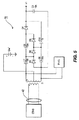
図5を参照すると、本発明の例となる実施形態に従ってネットワーク信号から動作電圧V1を生成するための回路70が示されている。図5に示されるように、回路70は複数のダイオードD1〜D4と、複数のキャパシタC2及びC7〜C10とを有する。これらの回路素子の例となる値が図5に示されているが、特定の用途に依存して他の値が使用されてもよい。図5で、ネットワーク入力部42及び第1の変圧器T1を介して受信されるネットワーク信号(例えば、イーサネット(登録商標)信号)は、スイッチアセンブリ50及びウォッチドッグ回路60に電力を供給するために使用されうる直流動作電圧V1を生成するよう回路素子D1〜D4並びにC2及びC7〜C10によって作用される。このようにして、スイッチアセンブリ50及びウォッチドッグ回路60は、有利に、ネットワークがアクティブである場合に常に電力を供給され得る。
Referring to FIG. 5, a
ここで記載されるように、ネットワークインターフェース装置は、次のステップ、すなわち、第1の変圧器(T1)の第1の側から第1のビデオ信号を受信し、前記第1の変圧器(T1)の第2の側で前記第1のビデオ信号を表す第2のビデオ信号を生成するステップと、制御信号に応答してスイッチアセンブリ(50)を動作させるステップと、該スイッチアセンブリ(50)が第1の状態で動作する場合に、前記第2のビデオ信号をネットワークデバイスのターミナル出力部(48)に結合し、前記第2のビデオ信号を前記ネットワークデバイスの前記ターミナル出力部(48)から第2の変圧器(T2)の第2の側に結合するステップと、前記スイッチアセンブリ(50)が第2の状態で動作する場合に、前記第2のビデオ信号を前記ターミナル出力部をバイパスしながら前記第2の変圧器(T2)の前記第2の側に結合するステップと、前記第2の変圧器(T2)の第1の側で前記第2のビデオ信号を表す第3のビデオ信号を生成するステップとを実行することができる。前記第3のビデオ信号は、次のネットワークインターフェース装置の入力部へ送信され得る。 As described herein, the network interface device receives a first video signal from a first side of the first transformer (T1), the first step (T1). ) Generating a second video signal representative of the first video signal on the second side, operating the switch assembly (50) in response to the control signal, the switch assembly (50) When operating in a first state, the second video signal is coupled to a terminal output (48) of the network device, and the second video signal is transmitted from the terminal output (48) of the network device. Coupling the second video signal to the second side of the second transformer (T2), and when the switch assembly (50) operates in the second state, A step of coupling to the second side of the second transformer (T2) while bypassing the final output; and the second video signal on the first side of the second transformer (T2). Generating a third video signal representative. The third video signal may be transmitted to the input unit of the next network interface device.
ここで記載されるように、本発明は、動作不能のネットワークデバイスをバイパスすることができるネットワークインターフェース装置を提供する。本発明は好ましい設計を有するよう記載されてきたが、本発明は、更に、本開示の精神及び適用範囲の中で変更されてよい。従って、本願は、その一般原理を用いて本発明のあらゆる変形例、使用、又は適応を網羅するよう意図される。更に、本願は、本発明が関連し且つ添付の特許請求の範囲の技術的範囲内にある当該技術における既知の又は習慣的な慣例の範囲内となる本開示からのこのような逸脱を網羅するよう意図される。 As described herein, the present invention provides a network interface device that can bypass an inoperable network device. While this invention has been described as having a preferred design, the present invention can be further modified within the spirit and scope of this disclosure. This application is therefore intended to cover any variations, uses, or adaptations of the invention using its general principles. Furthermore, this application covers such departures from the present disclosure which are within the scope of known or customary practice in the art to which this invention pertains and which are within the scope of the appended claims. Intended to be.
[関連出願の相互参照]
本願は、2007年7月23日に米国特許商標局で出願された仮出願(整理番号60/961,624)から生ずる優先権を主張するものである。
[Cross-reference of related applications]
This application claims priority arising from a provisional application (Docket No. 60 / 961,624) filed with the United States Patent and Trademark Office on July 23, 2007.
Claims (2)
第1の変圧器の第1の側から第1のビデオ信号を受信し、前記第1の変圧器の第2の側で前記第1のビデオ信号を表す第2のビデオ信号を生成するステップと、
制御信号に応答してスイッチアセンブリを動作させるステップと、
前記スイッチアセンブリが第1の動作状態である場合に、前記第2のビデオ信号をネットワークデバイスのターミナル入力部に与え、前記ネットワークデバイスのターミナル出力部を第2の変圧器の第2の側に結合するステップであって、前記ネットワークデバイスは前記ターミナル入力部から前記ネットワークデバイスの前記ターミナル出力部に前記第2のビデオ信号を流す、ステップと、
前記スイッチアセンブリが第2の動作状態である場合に、前記第1の変圧器の前記第2の側からの前記第2のビデオ信号を、前記ネットワークデバイスをバイパスしながら前記第2の変圧器の前記第2の側に直接的に与えるステップと、
前記第2の変圧器の第1の側で前記第2のビデオ信号を表す第3のビデオ信号を生成するステップと
を有する方法。 A method of bypassing an inoperable network device using only two transformers,
Receiving a first video signal from a first side of a first transformer and generating a second video signal representative of the first video signal at a second side of the first transformer; ,
Operating the switch assembly in response to the control signal;
When the switch assembly is in a first operating state, the second video signal is applied to a terminal input of a network device and the terminal output of the network device is coupled to a second side of a second transformer The network device passes the second video signal from the terminal input to the terminal output of the network device;
When the switch assembly is in a second operating state, the second video signal from the second side of the first transformer is routed through the second transformer while bypassing the network device. Providing directly to the second side;
Generating a third video signal representative of the second video signal on a first side of the second transformer.
第1及び第2の変圧器と、
第1のビデオ信号を受信するために前記第1の変圧器の第1の側に結合された第1の入力手段であって、前記第1の変圧器は該第1の変圧器の第2の側で前記第1のビデオ信号を表す第2のビデオ信号を生成する、第1の入力手段と、
前記第2の変圧器の第1の側に結合された第1の出力手段と、
ネットワークデバイスを介して第2の出力手段に結合された第2の入力手段と、
前記第1の変圧器の前記第2の側及び前記第2の変圧器の第2の側に結合されたスイッチング手段と
を有し、前記スイッチング手段が第1の状態である場合に、前記第1の変圧器の前記第2の側は前記第2の入力手段に結合され、前記ネットワークデバイスは前記第2の入力手段から前記第2の出力手段に前記第2のビデオ信号を流し、前記第2の変圧器の前記第2の側は前記第2の出力手段に結合され、前記スイッチング手段が第2の状態である場合に、前記ネットワークデバイスをバイパスしながら、前記第1の変圧器の前記第2の側は前記第2の変圧器の前記第2の側に結合されかつ前記第2の入力手段から分離され、前記第2のビデオ信号は前記第2の変圧器の前記第2の側に直接的に与えられる、ネットワークインターフェース装置。 A network interface device having only two transformers,
A first and a second transformer;
First input means coupled to a first side of the first transformer for receiving a first video signal, the first transformer being a second of the first transformer; First input means for generating a second video signal representative of the first video signal on the side of
First output means coupled to a first side of the second transformer;
Second input means coupled to the second output means via a network device;
Switching means coupled to the second side of the first transformer and the second side of the second transformer, and when the switching means is in a first state, The second side of one transformer is coupled to the second input means, and the network device passes the second video signal from the second input means to the second output means; The second side of the second transformer is coupled to the second output means, and when the switching means is in the second state, the second side of the first transformer is bypassed while bypassing the network device. A second side is coupled to the second side of the second transformer and is separated from the second input means, and the second video signal is the second side of the second transformer Network interface device directly attached to Place.
Applications Claiming Priority (3)
| Application Number | Priority Date | Filing Date | Title |
|---|---|---|---|
| US96162407P | 2007-07-23 | 2007-07-23 | |
| US60/961,624 | 2007-07-23 | ||
| PCT/US2008/007165 WO2009014581A1 (en) | 2007-07-23 | 2008-06-06 | Network interface apparatus for bypassing inoperable network device |
Publications (3)
| Publication Number | Publication Date |
|---|---|
| JP2010534446A JP2010534446A (en) | 2010-11-04 |
| JP2010534446A5 JP2010534446A5 (en) | 2011-06-02 |
| JP5507457B2 true JP5507457B2 (en) | 2014-05-28 |
Family
ID=39878923
Family Applications (1)
| Application Number | Title | Priority Date | Filing Date |
|---|---|---|---|
| JP2010518170A Active JP5507457B2 (en) | 2007-07-23 | 2008-06-06 | Method of bypassing inoperable network device and network interface apparatus |
Country Status (7)
| Country | Link |
|---|---|
| US (1) | US8842519B2 (en) |
| EP (1) | EP2171925A1 (en) |
| JP (1) | JP5507457B2 (en) |
| KR (1) | KR101477841B1 (en) |
| CN (1) | CN101772925B (en) |
| BR (1) | BRPI0814029A2 (en) |
| WO (1) | WO2009014581A1 (en) |
Families Citing this family (11)
| Publication number | Priority date | Publication date | Assignee | Title |
|---|---|---|---|---|
| EP2309678B1 (en) * | 2009-10-08 | 2013-04-24 | Nxp B.V. | An ethernet network component |
| DE102010029300A1 (en) * | 2010-05-26 | 2011-05-19 | Siemens Aktiengesellschaft | Interface for connecting subscribers of network utilized for e.g. controlling automation system in rail vehicle, has switching elements for automatically unlocking data bypass lines in deactivated operating condition of coupling unit |
| FR2969404B1 (en) | 2010-12-16 | 2013-01-04 | Schneider Electric Ind Sas | COMMUNICATION DEVICE AND ELECTRICAL BOARD COMPRISING SUCH A DEVICE |
| DE102012220974A1 (en) | 2011-11-25 | 2013-05-29 | Deutsches Zentrum für Luft- und Raumfahrt e.V. | Bus system i.e. Joint test action group chain, for e.g. testing digital and/or analog integrated circuits by boundary scan test, has switch input interconnected to output based on magnitude of control voltage applied at voltage terminal |
| EP2631806A1 (en) | 2012-02-27 | 2013-08-28 | Televic Rail NV | Devices and method for assigning network addresses |
| US9178564B2 (en) * | 2012-03-16 | 2015-11-03 | Schneider Electric Industries Sas | Communication cable breaker and method using same |
| EP2929676B1 (en) * | 2012-12-05 | 2017-07-26 | Siemens Canada Limited | A network device mounting rail for connecting removable modules |
| US9065810B2 (en) * | 2013-01-30 | 2015-06-23 | Ebay Inc. | Daisy chain distribution in data centers |
| JP6493958B2 (en) * | 2014-11-05 | 2019-04-03 | 日本電気株式会社 | Hub device and control system |
| US10284607B2 (en) | 2016-06-28 | 2019-05-07 | Simmonds Precision Products, Inc. | Selective bypassing of daisy-chained network devices |
| GB2560904B (en) | 2017-03-27 | 2020-06-10 | Ge Aviat Systems Ltd | Processor performance monitor |
Family Cites Families (24)
| Publication number | Priority date | Publication date | Assignee | Title |
|---|---|---|---|---|
| US4279034A (en) * | 1979-11-15 | 1981-07-14 | Bell Telephone Laboratories, Incorporated | Digital communication system fault isolation circuit |
| US4304001A (en) * | 1980-01-24 | 1981-12-01 | Forney Engineering Company | Industrial control system with interconnected remotely located computer control units |
| JPS58205352A (en) | 1982-05-25 | 1983-11-30 | Nissin Electric Co Ltd | Transmitting device |
| US4567482A (en) | 1982-11-12 | 1986-01-28 | The Babcock & Wilcox Company | Bypass control for stations in a communication system |
| JPS6038950A (en) | 1983-08-11 | 1985-02-28 | Sumitomo Electric Ind Ltd | Transmission line control system |
| US4620187A (en) * | 1984-12-11 | 1986-10-28 | International Business Machines Corp. | Transformer coupled, solid state communications line switch |
| US4628307A (en) * | 1984-12-18 | 1986-12-09 | International Business Machines Corp. | FET switch for high frequency signals |
| US4794632A (en) * | 1987-05-20 | 1988-12-27 | Minnesota Mining And Manufacturing Company | Telephone trunk line testing circuitry |
| JPH03108846A (en) * | 1989-09-22 | 1991-05-09 | Nec Corp | Loopback test equipment for transmission line |
| US5414708A (en) * | 1992-12-01 | 1995-05-09 | Farallon Computing, Inc. | Method and apparatus for connecting nodes for a computer network |
| US5577023A (en) * | 1992-12-01 | 1996-11-19 | Farallon Computing, Inc. | Method and apparatus for automatic configuration of a network connection |
| US5555456A (en) * | 1994-08-02 | 1996-09-10 | Itt Corporation | Reconfigurable fault control apparatus |
| GB2318262B (en) | 1996-10-08 | 2000-11-08 | Ibm | Bypass circuit for data processing system |
| US5796596A (en) * | 1996-11-15 | 1998-08-18 | Thomson Consumer Electronics, Inc. | Fault control circuit for switched power supply |
| US6448671B1 (en) * | 1999-08-05 | 2002-09-10 | Trw Inc. | Distributed vehicle safety system having fault protection |
| WO2005071953A1 (en) | 2004-01-23 | 2005-08-04 | Thomson Licensing | Selectable audio output configuration |
| JP5547372B2 (en) | 2004-08-27 | 2014-07-09 | トムソン ライセンシング | Apparatus and method for enabling digital and analog data communication over a data bus |
| EP1638260A1 (en) | 2004-09-20 | 2006-03-22 | Bombardier Transportation GmbH | Bypass switch for an ethernet-type network |
| EP1867113B1 (en) * | 2005-03-29 | 2009-10-14 | Panasonic Avionics Corporation | System and method for routing communication signals via a data distribution network |
| EP1883830B1 (en) * | 2005-05-18 | 2012-11-21 | Formation, Inc. | Solid-state ethernet by-pass switch circuitry |
| US7599485B2 (en) * | 2005-06-24 | 2009-10-06 | Cisco Technology, Inc. | Communications system employing single-pair identity circuit for remotely powered device |
| US20070025240A1 (en) * | 2005-07-29 | 2007-02-01 | Snide Todd A | Bypass switch for an ethernet device and method of bypassing devices in an ethernet network |
| US20070061056A1 (en) * | 2005-09-14 | 2007-03-15 | Bombardier Transportation Gmbh | Bypass switch for an ethernet-type network |
| US8009577B2 (en) * | 2007-04-02 | 2011-08-30 | Cisco Technology, Inc. | Automatic data rate and power adjustment on communications uplink based on communications activity on communications downlink |
-
2008
- 2008-06-06 EP EP08768238A patent/EP2171925A1/en not_active Withdrawn
- 2008-06-06 US US12/452,685 patent/US8842519B2/en active Active
- 2008-06-06 WO PCT/US2008/007165 patent/WO2009014581A1/en active Application Filing
- 2008-06-06 JP JP2010518170A patent/JP5507457B2/en active Active
- 2008-06-06 CN CN200880100434.1A patent/CN101772925B/en not_active Expired - Fee Related
- 2008-06-06 KR KR1020107001559A patent/KR101477841B1/en active IP Right Grant
- 2008-06-06 BR BRPI0814029-4A2A patent/BRPI0814029A2/en active Search and Examination
Also Published As
| Publication number | Publication date |
|---|---|
| WO2009014581A1 (en) | 2009-01-29 |
| KR101477841B1 (en) | 2014-12-30 |
| US8842519B2 (en) | 2014-09-23 |
| KR20100043194A (en) | 2010-04-28 |
| EP2171925A1 (en) | 2010-04-07 |
| BRPI0814029A2 (en) | 2015-02-03 |
| JP2010534446A (en) | 2010-11-04 |
| CN101772925B (en) | 2015-02-11 |
| US20100135151A1 (en) | 2010-06-03 |
| CN101772925A (en) | 2010-07-07 |
Similar Documents
| Publication | Publication Date | Title |
|---|---|---|
| JP5507457B2 (en) | Method of bypassing inoperable network device and network interface apparatus | |
| US7675849B2 (en) | System and method for routing communication signals via a data distribution network | |
| US9077641B2 (en) | Static ring network for vehicle communications | |
| US9154325B2 (en) | Apparatus and method for transferring data and energy via devices of a network | |
| US20060277589A1 (en) | System And Method For Presenting High-Quality Video | |
| US20080294918A1 (en) | Power signal merging for network interface devices | |
| JP2001190035A (en) | Multiple output uniterrupted power supply for communications system | |
| CN101129036B (en) | Transceiver with adjustable terminal network for a control device | |
| US20060238252A1 (en) | Network device with power potential rectifier | |
| US10469285B2 (en) | Bus system comprising a feed module and a load module | |
| US11516043B2 (en) | Monolithic high-voltage transceiver connected to two different supply voltage domains | |
| EP3131232B1 (en) | System and method for transmitting power over data lines | |
| US7532043B1 (en) | Signal detector output for cable driver applications | |
| FI3247015T4 (en) | Power supply device and method for operating a power supply device | |
| US20210184460A1 (en) | Power distribution system | |
| JP4911794B2 (en) | Receiver circuit, receiver system | |
| US7447273B2 (en) | Redundancy structure and method for high-speed serial link | |
| EP2862078B1 (en) | Coupling device for a data transmission network and data transmission network | |
| US20180069713A1 (en) | Dual power over ethernet redundancy | |
| US7899071B2 (en) | Serial bus structure | |
| CN110495141A (en) | The component and method for being used for transmission analog audio signal for aircraft | |
| KR102497158B1 (en) | Duplication apparatus in ethernet environment | |
| US11876367B2 (en) | Modularized DC interconnection device and system thereof | |
| US20230216491A1 (en) | Ethernet fail-safe relay | |
| JPH11308257A (en) | Digital network system |
Legal Events
| Date | Code | Title | Description |
|---|---|---|---|
| A521 | Written amendment |
Free format text: JAPANESE INTERMEDIATE CODE: A523 Effective date: 20110412 |
|
| A621 | Written request for application examination |
Free format text: JAPANESE INTERMEDIATE CODE: A621 Effective date: 20110412 |
|
| A131 | Notification of reasons for refusal |
Free format text: JAPANESE INTERMEDIATE CODE: A131 Effective date: 20120710 |
|
| A601 | Written request for extension of time |
Free format text: JAPANESE INTERMEDIATE CODE: A601 Effective date: 20121010 |
|
| A602 | Written permission of extension of time |
Free format text: JAPANESE INTERMEDIATE CODE: A602 Effective date: 20121017 |
|
| A521 | Written amendment |
Free format text: JAPANESE INTERMEDIATE CODE: A523 Effective date: 20121214 |
|
| A131 | Notification of reasons for refusal |
Free format text: JAPANESE INTERMEDIATE CODE: A131 Effective date: 20130122 |
|
| A601 | Written request for extension of time |
Free format text: JAPANESE INTERMEDIATE CODE: A601 Effective date: 20130419 |
|
| A602 | Written permission of extension of time |
Free format text: JAPANESE INTERMEDIATE CODE: A602 Effective date: 20130426 |
|
| A521 | Written amendment |
Free format text: JAPANESE INTERMEDIATE CODE: A523 Effective date: 20130702 |
|
| A131 | Notification of reasons for refusal |
Free format text: JAPANESE INTERMEDIATE CODE: A131 Effective date: 20130806 |
|
| A601 | Written request for extension of time |
Free format text: JAPANESE INTERMEDIATE CODE: A601 Effective date: 20131105 |
|
| A602 | Written permission of extension of time |
Free format text: JAPANESE INTERMEDIATE CODE: A602 Effective date: 20131112 |
|
| A521 | Written amendment |
Free format text: JAPANESE INTERMEDIATE CODE: A523 Effective date: 20140121 |
|
| TRDD | Decision of grant or rejection written | ||
| A01 | Written decision to grant a patent or to grant a registration (utility model) |
Free format text: JAPANESE INTERMEDIATE CODE: A01 Effective date: 20140218 |
|
| A61 | First payment of annual fees (during grant procedure) |
Free format text: JAPANESE INTERMEDIATE CODE: A61 Effective date: 20140319 |
|
| R150 | Certificate of patent or registration of utility model |
Ref document number: 5507457 Country of ref document: JP Free format text: JAPANESE INTERMEDIATE CODE: R150 |
|
| R250 | Receipt of annual fees |
Free format text: JAPANESE INTERMEDIATE CODE: R250 |
|
| S111 | Request for change of ownership or part of ownership |
Free format text: JAPANESE INTERMEDIATE CODE: R313113 |
|
| S531 | Written request for registration of change of domicile |
Free format text: JAPANESE INTERMEDIATE CODE: R313531 |
|
| R350 | Written notification of registration of transfer |
Free format text: JAPANESE INTERMEDIATE CODE: R350 |
|
| R250 | Receipt of annual fees |
Free format text: JAPANESE INTERMEDIATE CODE: R250 |