JP5493634B2 - Display device - Google Patents
Display device Download PDFInfo
- Publication number
- JP5493634B2 JP5493634B2 JP2009217182A JP2009217182A JP5493634B2 JP 5493634 B2 JP5493634 B2 JP 5493634B2 JP 2009217182 A JP2009217182 A JP 2009217182A JP 2009217182 A JP2009217182 A JP 2009217182A JP 5493634 B2 JP5493634 B2 JP 5493634B2
- Authority
- JP
- Japan
- Prior art keywords
- luminance
- information
- pixel
- deterioration
- display
- Prior art date
- Legal status (The legal status is an assumption and is not a legal conclusion. Google has not performed a legal analysis and makes no representation as to the accuracy of the status listed.)
- Active
Links
- 230000006866 deterioration Effects 0.000 claims description 150
- 230000015556 catabolic process Effects 0.000 claims description 53
- 238000006731 degradation reaction Methods 0.000 claims description 53
- 238000004364 calculation method Methods 0.000 claims description 30
- 238000012937 correction Methods 0.000 claims description 26
- 230000008859 change Effects 0.000 claims description 11
- 230000001186 cumulative effect Effects 0.000 claims description 2
- 235000019557 luminance Nutrition 0.000 description 319
- 230000006870 function Effects 0.000 description 58
- 238000012545 processing Methods 0.000 description 57
- 238000000034 method Methods 0.000 description 28
- 230000001133 acceleration Effects 0.000 description 16
- 238000005070 sampling Methods 0.000 description 12
- 238000010586 diagram Methods 0.000 description 10
- 230000010354 integration Effects 0.000 description 10
- 238000007789 sealing Methods 0.000 description 8
- 239000010408 film Substances 0.000 description 5
- 238000005259 measurement Methods 0.000 description 5
- 230000004044 response Effects 0.000 description 5
- 239000003990 capacitor Substances 0.000 description 3
- 230000004048 modification Effects 0.000 description 3
- 238000012986 modification Methods 0.000 description 3
- 230000003287 optical effect Effects 0.000 description 3
- 239000000758 substrate Substances 0.000 description 3
- 230000007704 transition Effects 0.000 description 3
- 230000007423 decrease Effects 0.000 description 2
- 230000007547 defect Effects 0.000 description 2
- 238000009795 derivation Methods 0.000 description 2
- 230000000694 effects Effects 0.000 description 2
- 239000004973 liquid crystal related substance Substances 0.000 description 2
- 230000002123 temporal effect Effects 0.000 description 2
- 230000002238 attenuated effect Effects 0.000 description 1
- 238000006243 chemical reaction Methods 0.000 description 1
- 230000002542 deteriorative effect Effects 0.000 description 1
- 238000005401 electroluminescence Methods 0.000 description 1
- 239000011521 glass Substances 0.000 description 1
- 230000002427 irreversible effect Effects 0.000 description 1
- 239000011159 matrix material Substances 0.000 description 1
- 230000008569 process Effects 0.000 description 1
- 239000010409 thin film Substances 0.000 description 1
- 230000036962 time dependent Effects 0.000 description 1
Images


Classifications
-
- G—PHYSICS
- G09—EDUCATION; CRYPTOGRAPHY; DISPLAY; ADVERTISING; SEALS
- G09G—ARRANGEMENTS OR CIRCUITS FOR CONTROL OF INDICATING DEVICES USING STATIC MEANS TO PRESENT VARIABLE INFORMATION
- G09G3/00—Control arrangements or circuits, of interest only in connection with visual indicators other than cathode-ray tubes
- G09G3/20—Control arrangements or circuits, of interest only in connection with visual indicators other than cathode-ray tubes for presentation of an assembly of a number of characters, e.g. a page, by composing the assembly by combination of individual elements arranged in a matrix no fixed position being assigned to or needed to be assigned to the individual characters or partial characters
- G09G3/22—Control arrangements or circuits, of interest only in connection with visual indicators other than cathode-ray tubes for presentation of an assembly of a number of characters, e.g. a page, by composing the assembly by combination of individual elements arranged in a matrix no fixed position being assigned to or needed to be assigned to the individual characters or partial characters using controlled light sources
- G09G3/30—Control arrangements or circuits, of interest only in connection with visual indicators other than cathode-ray tubes for presentation of an assembly of a number of characters, e.g. a page, by composing the assembly by combination of individual elements arranged in a matrix no fixed position being assigned to or needed to be assigned to the individual characters or partial characters using controlled light sources using electroluminescent panels
- G09G3/32—Control arrangements or circuits, of interest only in connection with visual indicators other than cathode-ray tubes for presentation of an assembly of a number of characters, e.g. a page, by composing the assembly by combination of individual elements arranged in a matrix no fixed position being assigned to or needed to be assigned to the individual characters or partial characters using controlled light sources using electroluminescent panels semiconductive, e.g. using light-emitting diodes [LED]
- G09G3/3208—Control arrangements or circuits, of interest only in connection with visual indicators other than cathode-ray tubes for presentation of an assembly of a number of characters, e.g. a page, by composing the assembly by combination of individual elements arranged in a matrix no fixed position being assigned to or needed to be assigned to the individual characters or partial characters using controlled light sources using electroluminescent panels semiconductive, e.g. using light-emitting diodes [LED] organic, e.g. using organic light-emitting diodes [OLED]
- G09G3/3225—Control arrangements or circuits, of interest only in connection with visual indicators other than cathode-ray tubes for presentation of an assembly of a number of characters, e.g. a page, by composing the assembly by combination of individual elements arranged in a matrix no fixed position being assigned to or needed to be assigned to the individual characters or partial characters using controlled light sources using electroluminescent panels semiconductive, e.g. using light-emitting diodes [LED] organic, e.g. using organic light-emitting diodes [OLED] using an active matrix
- G09G3/3233—Control arrangements or circuits, of interest only in connection with visual indicators other than cathode-ray tubes for presentation of an assembly of a number of characters, e.g. a page, by composing the assembly by combination of individual elements arranged in a matrix no fixed position being assigned to or needed to be assigned to the individual characters or partial characters using controlled light sources using electroluminescent panels semiconductive, e.g. using light-emitting diodes [LED] organic, e.g. using organic light-emitting diodes [OLED] using an active matrix with pixel circuitry controlling the current through the light-emitting element
-
- G—PHYSICS
- G09—EDUCATION; CRYPTOGRAPHY; DISPLAY; ADVERTISING; SEALS
- G09G—ARRANGEMENTS OR CIRCUITS FOR CONTROL OF INDICATING DEVICES USING STATIC MEANS TO PRESENT VARIABLE INFORMATION
- G09G2320/00—Control of display operating conditions
- G09G2320/02—Improving the quality of display appearance
- G09G2320/029—Improving the quality of display appearance by monitoring one or more pixels in the display panel, e.g. by monitoring a fixed reference pixel
-
- G—PHYSICS
- G09—EDUCATION; CRYPTOGRAPHY; DISPLAY; ADVERTISING; SEALS
- G09G—ARRANGEMENTS OR CIRCUITS FOR CONTROL OF INDICATING DEVICES USING STATIC MEANS TO PRESENT VARIABLE INFORMATION
- G09G2320/00—Control of display operating conditions
- G09G2320/04—Maintaining the quality of display appearance
- G09G2320/043—Preventing or counteracting the effects of ageing
- G09G2320/048—Preventing or counteracting the effects of ageing using evaluation of the usage time
-
- G—PHYSICS
- G09—EDUCATION; CRYPTOGRAPHY; DISPLAY; ADVERTISING; SEALS
- G09G—ARRANGEMENTS OR CIRCUITS FOR CONTROL OF INDICATING DEVICES USING STATIC MEANS TO PRESENT VARIABLE INFORMATION
- G09G2360/00—Aspects of the architecture of display systems
- G09G2360/14—Detecting light within display terminals, e.g. using a single or a plurality of photosensors
- G09G2360/145—Detecting light within display terminals, e.g. using a single or a plurality of photosensors the light originating from the display screen
Landscapes
- Engineering & Computer Science (AREA)
- Physics & Mathematics (AREA)
- Computer Hardware Design (AREA)
- General Physics & Mathematics (AREA)
- Theoretical Computer Science (AREA)
- Control Of Indicators Other Than Cathode Ray Tubes (AREA)
- Electroluminescent Light Sources (AREA)
- Control Of El Displays (AREA)
Description
本発明は、表示パネルに発光素子が設けられた表示装置に関する。 The present invention relates to a display device in which a light emitting element is provided on a display panel.
近年、画像表示を行う表示装置の分野では、画素の発光素子として、流れる電流値に応じて発光輝度が変化する電流駆動型の光学素子、例えば有機EL(electro luminescence)素子を用いた表示装置が開発され、商品化が進められている。有機EL素子は、液晶素子などと異なり自発光素子である。そのため、有機EL素子を用いた表示装置(有機EL表示装置)では、光源(バックライト)が必要ないので、光源を必要とする液晶表示装置と比べて、薄型化、高輝度化することができる。特に、駆動方式としてアクティブマトリクス方式を用いた場合には、各画素をホールド点灯させることができ、低消費電力化することもできる。そのため、有機EL表示装置は、次世代のフラットパネルディスプレイの主流になると期待されている。 In recent years, in the field of display devices that perform image display, display devices that use current-driven optical elements, such as organic EL (electroluminescence) elements, whose light emission luminance changes according to the value of a flowing current are used as light emitting elements of pixels. Developed and commercialized. Unlike a liquid crystal element or the like, the organic EL element is a self-luminous element. Therefore, a display device (organic EL display device) using an organic EL element does not require a light source (backlight), so that it can be made thinner and brighter than a liquid crystal display device that requires a light source. . In particular, when the active matrix method is used as the driving method, each pixel can be lighted on hold and power consumption can be reduced. Therefore, organic EL display devices are expected to become the mainstream of next-generation flat panel displays.
しかし、有機EL素子では、通電する電流量に応じて素子が劣化し、輝度が低下するという問題がある。そのため、有機EL素子を表示装置の画素として用いた場合には、画素ごとに劣化の状況が異なることがある。例えば、時刻や表示チャンネルなどの情報が長時間、同じ場所に高輝度で表示されていた場合には、その部分の画素だけ劣化が早まる。その結果、劣化の早まった画素を含む部分に高輝度の映像が表示された場合には、劣化の早まった画素の部分だけが暗く表示される焼き付きという現象が生じてしまう。この焼き付きは非可逆性であることから、一旦、焼き付きが生じると、焼き付きが消えることはない。 However, the organic EL element has a problem that the element deteriorates in accordance with the amount of current to be applied and the luminance decreases. Therefore, when an organic EL element is used as a pixel of a display device, the state of deterioration may be different for each pixel. For example, when information such as time and display channel is displayed at the same place with high luminance for a long time, the deterioration of only the pixels in that portion is accelerated. As a result, when a high-luminance image is displayed in a portion including a pixel that has deteriorated quickly, a phenomenon of image sticking occurs in which only the portion of the pixel that has deteriorated rapidly is displayed darkly. Since this seizure is irreversible, once seizure occurs, the seizure does not disappear.
焼き付きを防止する手法は、今までに多数提案されている。例えば、特許文献1では、表示領域外にダミー画素を設け、ダミー画素を発光させたときの端子電圧を検出することによりダミー画素の劣化度合いを見積もり、その見積もりを利用して映像信号を補正する方法が開示されている。また、例えば、特許文献2,3では、各表示画素内に光センサを配置し、光センサから出力される受光信号を利用して映像信号を補正する方法が開示されている。
Many methods for preventing burn-in have been proposed so far. For example, in
しかし、特許文献1の手法では、表示領域内の画素の発光情報に基づいて画素の劣化度合いが見積もられておらず、映像信号を正確に補正することが不可能であることから、焼き付きを防止することはできないという問題があった。また、特許文献2,3の手法では、各画素内の光センサの光電変換効率がばらつくので、例えば、同一輝度を表示している2つの画素において、受光信号の大きさが異なってしまうことがある。その結果、正確に焼き付きを防止することができないという問題があった。
However, in the method of
本発明はかかる問題点に鑑みてなされたものであり、その目的は、正確に焼き付きを防止することの可能な表示装置を提供することにある。 The present invention has been made in view of such problems, and an object of the present invention is to provide a display device capable of accurately preventing burn-in.
本発明による表示装置は、複数の表示画素が2次元配置された表示領域と、複数のダミー画素が配置された非表示領域とを有する表示パネルを備えたものである。本発明による表示装置は、また、各ダミー画素に互いに異なる大きさの定電流を流して各ダミー画素を発光させる第1駆動部と、各ダミー画素の発光光を検知して各ダミー画素の輝度情報を出力する受光部と、前記受光部の出力を用いて所定の演算を行う演算部とを備えている。ここで、演算部は、第1演算部、第2演算部、および第3演算部を有している。第1演算部は、複数のダミー画素のうちの一の画素である基準画素の第1輝度情報から基準画素の第1輝度劣化情報を導出すると共に、複数のダミー画素のうち基準画素を除く全ての画素である複数の非基準画素の第2輝度情報から各非基準画素の第2輝度劣化情報を導出するようになっている。第2演算部は、第1輝度劣化情報および第2輝度劣化情報から、第1輝度情報に対する第2輝度情報のべき係数を導出するようになっている。第3演算部は、第1輝度情報から基準画素の輝度の経時変化を表す第1輝度劣化関数を導出すると共に、第1輝度劣化関数およびべき係数から、非基準画素の輝度の経時変化を表す第2輝度劣化関数を導出するようになっている。演算部は、さらに、第1輝度劣化関数、第2輝度劣化関数、および各表示画素の映像信号の履歴から、各表示画素の輝度劣化率を予測し、予測した各表示画素の輝度劣化率と、表示パネルのガンマ特性とから映像信号に対する補正量を導出する第4演算部を有している。本発明による表示装置は、さらに、補正量を用いて映像信号を補正し、補正後の映像信号を複数の表示画素に出力する第2駆動部を備えている。 A display device according to the present invention includes a display panel having a display area in which a plurality of display pixels are two-dimensionally arranged and a non-display area in which a plurality of dummy pixels are arranged. The display device according to the present invention also includes a first driving unit for causing each dummy pixel to emit light by flowing constant currents of different magnitudes to each dummy pixel, and detecting the light emitted from each dummy pixel to detect the luminance of each dummy pixel. A light receiving unit that outputs information and a calculation unit that performs a predetermined calculation using the output of the light receiving unit are provided. Here, the computing unit includes a first computing unit, a second computing unit, and a third computing unit. The first calculation unit derives the first luminance deterioration information of the reference pixel from the first luminance information of the reference pixel that is one pixel of the plurality of dummy pixels, and all of the plurality of dummy pixels excluding the reference pixel The second luminance deterioration information of each non-reference pixel is derived from the second luminance information of a plurality of non-reference pixels that are the non-reference pixels. The second calculation unit derives a power coefficient of the second luminance information with respect to the first luminance information from the first luminance deterioration information and the second luminance deterioration information. The third calculation unit derives a first luminance deterioration function that represents a temporal change in the luminance of the reference pixel from the first luminance information, and represents a temporal change in the luminance of the non-reference pixel from the first luminance deterioration function and the power coefficient. A second luminance deterioration function is derived. The calculation unit further predicts the luminance deterioration rate of each display pixel from the first luminance deterioration function, the second luminance deterioration function, and the history of the video signal of each display pixel, and the predicted luminance deterioration rate of each display pixel and And a fourth arithmetic unit for deriving a correction amount for the video signal from the gamma characteristic of the display panel. The display device according to the present invention further includes a second drive unit that corrects the video signal using the correction amount and outputs the corrected video signal to a plurality of display pixels.
本発明による表示装置では、表示パネルの非表示領域に設けられた各ダミー画素に、互いに異なる大きさの定電流が流され、その定電流の大きさに応じた輝度で各ダミー画素が発光し、各ダミー画素の発光光が受光部で検知され、各ダミー画素の輝度情報が受光部から出力される。その後、基準画素の第1輝度情報から導出された第1輝度劣化情報と、各非基準画素の第2輝度情報から導出された第2輝度劣化情報とから、第1輝度情報に対する第2輝度情報のべき係数が導出される。さらに、第1輝度情報から第1輝度劣化関数が導出されると共に、第1輝度劣化関数およびべき係数から第2輝度劣化関数が導出される。これにより、例えば、第1輝度劣化関数と、第1輝度劣化関数およびべき係数から得られた第2輝度劣化関数と、各表示画素の映像信号の履歴とを利用して、各表示画素の輝度劣化率を予測することができる。 In the display device according to the present invention, constant currents having different magnitudes are passed through the dummy pixels provided in the non-display area of the display panel, and each dummy pixel emits light with a luminance corresponding to the magnitude of the constant current. The light emitted from each dummy pixel is detected by the light receiving unit, and the luminance information of each dummy pixel is output from the light receiving unit. Thereafter, the second luminance information for the first luminance information is derived from the first luminance degradation information derived from the first luminance information of the reference pixel and the second luminance degradation information derived from the second luminance information of each non-reference pixel. The power coefficient of is derived. Furthermore, a first luminance degradation function is derived from the first luminance information, and a second luminance degradation function is derived from the first luminance degradation function and the power coefficient. Thereby, for example, the luminance of each display pixel is obtained using the first luminance deterioration function, the second luminance deterioration function obtained from the first luminance deterioration function and the power coefficient, and the history of the video signal of each display pixel. The deterioration rate can be predicted.
ここで、本発明による表示装置において、第3演算部は、第1輝度情報のうち最新の輝度情報と、第1輝度情報のうち最新ではない輝度情報とに合うように、第1輝度劣化関数のパラメータを更新してもよい。さらに、第3演算部は、第1輝度劣化関数のパラメータが更新された後の第1輝度劣化関数、およびべき係数から、第2輝度劣化関数のパラメータを更新してもよい。 Here, in the display device according to the present invention, the third calculation unit includes the first luminance deterioration function so as to match the latest luminance information among the first luminance information and the non-latest luminance information among the first luminance information. The parameters may be updated. Further, the third calculation unit may update the parameter of the second luminance degradation function from the first luminance degradation function and the power coefficient after the parameter of the first luminance degradation function is updated.
また、本発明による表示装置において、第1演算部は、第1輝度劣化情報および第2輝度劣化情報を、例えば、以下の2つの方法のうちいずれか一方を用いることによって導出してもよい。 In the display device according to the present invention, the first arithmetic unit may derive the first luminance deterioration information and the second luminance deterioration information by using one of the following two methods, for example.
(1つ目の方法)
1つ目の方法において、第1輝度劣化情報は、第1輝度情報のうち最新の輝度情報の対数をとることにより得られた値と、第1輝度情報のうち最新ではない輝度情報の対数をとることにより得られた値との差分をとることにより導出される。また、第2輝度劣化情報は、第2輝度情報のうち最新の輝度情報の対数をとることにより得られた値と、第2輝度情報のうち最新ではない輝度情報の対数をとることにより得られた値との差分をとることにより導出される。
(First method)
In the first method, the first luminance deterioration information includes a value obtained by taking a logarithm of the latest luminance information among the first luminance information and a logarithm of the luminance information which is not the latest among the first luminance information. It is derived by taking the difference from the value obtained by taking. The second luminance deterioration information is obtained by taking the logarithm of the latest luminance information of the second luminance information and the logarithm of the luminance information which is not the latest of the second luminance information. It is derived by taking the difference from the measured value.
(2つ目の方法)
2つ目の方法において、第1輝度劣化情報は、第1輝度情報のうち最新の輝度情報と、第1輝度情報のうち最新ではない輝度情報との差分をとることにより導出される。また、第2輝度劣化情報は、第2輝度情報のうち最新の輝度情報と、第2輝度情報のうち最新ではない輝度情報との差分をとることにより導出される。
(Second method)
In the second method, the first luminance deterioration information is derived by taking a difference between the latest luminance information in the first luminance information and the luminance information that is not the latest in the first luminance information. The second luminance deterioration information is derived by taking a difference between the latest luminance information in the second luminance information and the luminance information that is not the latest in the second luminance information.
また、本発明による表示装置において、第2演算部は、べき係数を、例えば、上述の方法を用いて導出した第2輝度劣化情報を、上述の方法を用いて導出した第1輝度劣化情報で除算することにより導出してもよい。また、本発明による表示装置において、第1演算部は、第1輝度劣化情報および第2輝度劣化情報を導出する周期(サンプリング周期)を、複数のダミー画素の発光累積時間に応じて変化させてもよい。 Further, in the display device according to the present invention, the second arithmetic unit uses the first luminance deterioration information derived using the above-described method as the power coefficient, for example, the second luminance deterioration information derived using the above-described method. It may be derived by dividing. Further, in the display device according to the present invention, the first calculation unit changes a cycle (sampling cycle) for deriving the first luminance deterioration information and the second luminance deterioration information according to the light emission cumulative time of the plurality of dummy pixels. Also good.
また、本発明による表示装置において、複数の第1ダミー画素のうち低輝度で発光させる複数の低輝度画素が、それぞれ、複数の第2ダミー画素によって構成されていてもよい。そのようにした場合であって、複数の低輝度画素に基準画素が含まれるときには、第1演算部は、基準画素に含まれる複数の第2ダミー画素の輝度情報の平均値から第1輝度劣化情報を導出することが可能である。また、複数の低輝度画素に非基準画素が含まれるときには、第1演算部は、低輝度画素であって、かつ非基準画素である画素に含まれる複数の第2ダミー画素の輝度情報の平均値から第2輝度劣化情報を導出することが可能である。 In the display device according to the present invention, the plurality of low-luminance pixels that emit light with low luminance among the plurality of first dummy pixels may be configured by a plurality of second dummy pixels, respectively. In such a case, when the reference pixel is included in the plurality of low luminance pixels, the first calculation unit calculates the first luminance deterioration from the average value of the luminance information of the plurality of second dummy pixels included in the reference pixel. It is possible to derive information. In addition, when the non-reference pixel is included in the plurality of low-luminance pixels, the first arithmetic unit is an average of the luminance information of the plurality of second dummy pixels included in the pixel that is the low-luminance pixel and is the non-reference pixel. It is possible to derive the second luminance deterioration information from the value.
また、本発明による表示装置において、基準画素の輝度が所定の値以下となった場合には、第1演算部は、複数の非基準画素のうちの一の画素を新たな基準画素に設定してもよい。そのようにした場合には、第1演算部は、その新たな基準画素の輝度情報から第1輝度劣化情報を導出すると共に、複数の非基準画素のうち新たに基準画素として設定された画素を除く全ての画素の第2輝度情報から各非基準画素の第2輝度劣化情報を導出することが可能である。 In the display device according to the present invention, when the luminance of the reference pixel becomes equal to or lower than a predetermined value, the first calculation unit sets one pixel among the plurality of non-reference pixels as a new reference pixel. May be. In such a case, the first calculation unit derives the first luminance deterioration information from the luminance information of the new reference pixel, and selects a pixel newly set as the reference pixel among the plurality of non-reference pixels. It is possible to derive the second luminance deterioration information of each non-reference pixel from the second luminance information of all the pixels other than the pixels.
本発明による表示装置によれば、例えば、第1輝度劣化関数と、第1輝度劣化関数およびべき係数から得られた第2輝度劣化関数と、各表示画素の映像信号の履歴とを利用して、各表示画素の輝度劣化率を予測することができるようにした。これにより、高い精度で各表示画素の輝度劣化を予測することができるので、正確に焼き付きを防止することができる。 According to the display device of the present invention, for example, using the first luminance degradation function, the second luminance degradation function obtained from the first luminance degradation function and the power coefficient, and the video signal history of each display pixel. The luminance deterioration rate of each display pixel can be predicted. Thereby, since the luminance degradation of each display pixel can be predicted with high accuracy, burn-in can be prevented accurately.
また、本発明による表示装置において、第1輝度情報のうち最新の輝度情報と、第1輝度情報のうち最新ではない輝度情報とに合うように、第1輝度劣化関数のパラメータを更新すると共に、第1輝度劣化関数のパラメータが更新された後の第1輝度劣化関数、およびべき係数から、第2輝度劣化関数のパラメータを更新するようにした場合には、観測時点のデータで、各表示画素の輝度劣化率を予測することができる。これにより、更新に必要なメモリ量および計算量を小さく抑えることができる。 Further, in the display device according to the present invention, the parameter of the first luminance degradation function is updated so as to match the latest luminance information of the first luminance information and the non-latest luminance information of the first luminance information, first luminance degradation function after parameters of the first luminance degradation function is updated, the contact and to coefficients, when to update the parameters of the second luminance degradation function, the data of the observation point, each display The luminance deterioration rate of the pixel can be predicted. As a result, the amount of memory and the amount of calculation required for updating can be kept small.
また、本発明による表示装置において、サンプリング周期を複数のダミー画素の発光累積時間に応じて変化させるようにした場合には、例えば、発光累積時間が長時間に達し、輝度劣化があまり生じなくなったときに、サンプリング周期を長くすることができる。これにより、更新に必要な計算量を小さく抑えることができる。 Further, in the display device according to the present invention, when the sampling period is changed according to the accumulated light emission times of the plurality of dummy pixels, for example, the accumulated light emission time reaches a long time, and the luminance degradation does not occur much. Sometimes the sampling period can be lengthened. As a result, the amount of calculation required for updating can be kept small.
また、本発明による表示装置において、各低輝度画素を複数の第2ダミー画素によって構成し、複数の第2ダミー画素の輝度情報の平均値から第1輝度劣化情報または第2輝度劣化情報を導出するようにした場合には、低輝度の第1ダミー画素における測定誤差を小さくすることができる。これにより、高い精度で低輝度の表示画素の輝度劣化を予測することができるので、焼き付きをより一層、正確に防止することができる。 In the display device according to the present invention, each low-luminance pixel is constituted by a plurality of second dummy pixels, and the first luminance deterioration information or the second luminance deterioration information is derived from the average value of the luminance information of the plurality of second dummy pixels. In such a case, the measurement error in the first dummy pixel with low brightness can be reduced. As a result, it is possible to predict the luminance deterioration of the low-luminance display pixel with high accuracy, so that burn-in can be prevented more accurately.
また、本発明による表示装置において、基準画素の輝度が所定の値以下となった場合に、複数の非基準画素のうちの一の画素を新たな基準画素に設定し、第1輝度劣化情報および第2輝度劣化情報を導出するようにしたときには、基準画素に不具合が生じた場合でも、継続して、輝度劣化を予測することができる。これにより、輝度劣化の予測の信頼性を高めることができる。 In the display device according to the present invention, when the luminance of the reference pixel becomes equal to or lower than a predetermined value, one pixel of the plurality of non-reference pixels is set as a new reference pixel, and the first luminance deterioration information and When the second luminance deterioration information is derived, it is possible to predict the luminance deterioration continuously even when a defect occurs in the reference pixel. Thereby, the reliability of prediction of luminance degradation can be improved.
以下、発明を実施するための形態について、図面を参照して詳細に説明する。なお、説明は以下の順序で行う。
1.実施の形態(図1〜図16)
2.変形例(図なし)
・初期輝度Yiの低い各ダミー画素16を複数のダミー画素で構成した例
・基準画素に不具合が生じた場合に別のダミー画素16を新たな基準画素に設定 するようにした例
・サンプリング周期ΔTを可変にした例
・四則演算だけで、べき係数n(Yi,Ys)を導出するようにした例
3.適用例(図17〜図21)
DESCRIPTION OF EMBODIMENTS Hereinafter, embodiments for carrying out the invention will be described in detail with reference to the drawings. The description will be given in the following order.
1. Embodiment (FIGS. 1 to 16)
2. Modified example (not shown)
Initial luminance Y i each dummy pixel example, sampling period so as to set a
<実施の形態>
(表示装置1の概略構成)
図1は、本発明の一実施の形態に係る表示装置1の概略構成を表したものである。この表示装置1は、表示パネル10と、表示パネル10を駆動する駆動回路20とを備えている。
<Embodiment>
(Schematic configuration of the display device 1)
FIG. 1 shows a schematic configuration of a
表示パネル10は、複数の有機EL素子11R,11G,11Bが2次元配置された表示領域12を有している。本実施の形態では、互いに隣り合う3つの有機EL素子11R,11G,11Bが1つの画素(表示画素13)を構成している。なお、以下では、有機EL素子11R,11G,11Bの総称として有機EL素子11を適宜、用いるものとする。表示パネル10は、また、複数の有機EL素子14R,14G,14Bが2次元配置された非表示領域15を有している。本実施の形態では、互いに隣り合う3つの有機EL素子14R,14G,14Bが1つの画素(ダミー画素16)を構成している。なお、以下では、有機EL素子14R,14G,14Bの総称として有機EL素子14を適宜、用いるものとする。非表示領域15には、さらに、有機EL素子14R,14G,14Bから発せられた光を受光する受光素子群17(受光部)が設けられている。受光素子群17は、例えば、図示しないが、複数の受光素子からなる。複数の受光素子は、例えば、個々の有機EL素子14と対となって2次元配置されており、各受光素子は、各ダミー画素16(各有機EL素子14)から発せられた光(発光光)を検知して、各ダミー画素16の受光信号17A(輝度情報)を出力するようになっている。各受光素子は、例えば、フォトダイオードである。
The
駆動回路20は、タイミング生成回路21、映像信号処理回路22、信号線駆動回路23、走査線駆動回路24、ダミー画素・受光素子群駆動回路25、受光信号処理回路26および記憶回路27を有している。
The driving
(画素回路18)
図2は、表示領域12内の回路構成の一例を表したものである。表示領域12内には、複数の画素回路18が個々の有機EL素子11と対となって2次元配置されている。各画素回路18は、例えば、駆動トランジスタTr1、書き込みトランジスタTr2および保持容量Csによって構成されたものであり、2Tr1Cの回路構成となっている。駆動トランジスタTr1および書き込みトランジスタTr2は、例えば、nチャネルMOS型の薄膜トランジスタ(TFT(Thin Film Transistor))により形成されている。駆動トランジスタTr1または書き込みトランジスタTr2は、pチャネルMOS型のTFTであってもよい。
(Pixel circuit 18)
FIG. 2 shows an example of a circuit configuration in the
表示領域12において、列方向には信号線DTLが複数配置され、行方向には走査線WSLおよび電源線Vccがそれぞれ複数配置されている。各信号線DTLと各走査線WSLとの交差点近傍には、有機EL素子11R,11G,11Bのいずれか一つ(サブピクセル)が設けられている。各信号線DTLは、信号線駆動回路23の出力端(図示せず)と、書き込みトランジスタTr2のドレイン電極(図示せず)に接続されている。各走査線WSLは、走査線駆動回路24の出力端(図示せず)と、書き込みトランジスタTr2のゲート電極(図示せず)に接続されている。各電源線Vccは、電源の出力端(図示せず)と、駆動トランジスタTr1のドレイン電極(図示せず)に接続されている。書き込みトランジスタTr2のソース電極(図示せず)は、駆動トランジスタTr1のゲート電極(図示せず)と、保持容量Csの一端に接続されている。駆動トランジスタTr1のソース電極(図示せず)と保持容量Csの他端とが、有機EL素子11のアノード電極(図示せず)に接続されている。有機EL素子11のカソード電極(図示せず)は、例えば、グラウンド線GNDに接続されている。
In the
(表示パネル10の上面構成)
図3は、表示パネル10の上面構成の一例を表したものである。表示パネル10は、例えば、駆動パネル30と封止パネル40とが封止層(図示せず)を介して貼り合わされた構造となっている。
(Top panel configuration of display panel 10)
FIG. 3 illustrates an example of a top surface configuration of the
駆動パネル30は、図3に示していないが、表示領域12に、2次元配置された複数の有機EL素子11と、各有機EL素子11に隣接して配置された複数の画素回路18とを有している。駆動パネル30は、また、図3に示していないが、非表示領域15に、2次元配置された複数の有機EL素子14と、各有機EL素子14に隣接して配置された複数の受光素子とを有している。
Although not shown in FIG. 3, the drive panel 30 includes a plurality of
駆動パネル30の一辺(長辺)には、例えば、図3に示したように、複数の映像信号供給TAB51と、制御信号供給TCP54と、受光信号出力TCP55とが取り付けられている。駆動パネル30の他の辺(短辺)には、例えば、走査信号供給TAB52が取り付けられている。また、駆動パネル30の一辺(長辺)であって、かつ映像信号供給TAB51とは異なる辺には、例えば、電源供給TCP53が取り付けられている。映像信号供給TAB51は、信号線駆動回路23の集積されたICをフィルム状の配線基板の開口に中空配線したものである。走査信号供給TAB52は、走査線駆動回路24の集積されたICをフィルム状の配線基板の開口に中空配線したものである。電源供給TCP53は、外部の電源と電源線Vccとを互いに電気的に接続する複数の配線がフィルム上に形成されたものである。制御信号供給TCP54は、外部のダミー画素・受光素子群駆動回路25と、ダミー画素16および受光素子群17とを互いに電気的に接続する複数の配線がフィルム上に形成されたものである。受光信号出力TCP55は、外部の受光信号処理回路26と、受光素子群17とを互いに電気的に接続する複数の配線がフィルム上に形成されたものである。なお、信号線駆動回路23および走査線駆動回路24は、TABに形成されていなくてもよく、例えば、駆動パネル30に形成されていてもよい。
For example, as shown in FIG. 3, a plurality of video
封止パネル40は、例えば、有機EL素子11,14を封止する封止基板(図示せず)と、カラーフィルタ(図示せず)とを有している。カラーフィルタは、例えば、封止基板の表面のうち有機EL素子11の光が通過する領域に設けられている。カラーフィルタは、例えば、有機EL素子11R,11G,11Bのそれぞれに対応して、赤色用のフィルタ、緑色用のフィルタおよび青色用のフィルタ(図示せず)を有している。封止パネル40は、例えば、さらに、光反射部(図示せず)を有している。光反射部は、有機EL素子14から発せられた光を反射して、受光素子群17に入射させるものであり、例えば、封止基板の表面のうち有機EL素子14の光が通過する領域に設けられている。
The sealing
(駆動回路20)
次に、駆動回路20内の各回路について、図1を参照して説明する。タイミング生成回路21は、映像信号処理回路22、信号線駆動回路23、走査線駆動回路24、ダミー画素・受光素子群駆動回路25、および受光信号処理回路26が連動して動作するように制御するものである。
(Drive circuit 20)
Next, each circuit in the
タイミング生成回路21は、例えば、外部から入力された同期信号20Bに応じて(同期して)、上述した各回路に対して制御信号21Aを出力するようになっている。タイミング生成回路21は、例えば、映像信号処理回路22、ダミー画素・受光素子群駆動回路25、受光信号処理回路26および記憶回路27などと共に、例えば、表示パネル10とは別体の制御回路基板(図示せず)上に形成されている。
The timing generation circuit 21 outputs a control signal 21A to each circuit described above, for example, in response to (in synchronization with) the
映像信号処理回路22は、例えば、制御信号21Aの入力に応じて(同期して)、外部から入力されたデジタルの映像信号20Aを補正すると共に、補正した後の映像信号をアナログに変換して信号線駆動回路23に出力するものである。本実施の形態では、映像信号処理回路22は、記憶回路27から読み出した補正情報26A(後述)を用いて映像信号20Aを補正するようになっている。映像信号処理回路22は、例えば、一水平期間ごとに、記憶回路27から、補正情報26Aとして1ライン分の各表示画素13の補正量ΔSxy(後述)を読み出し、読み出した補正量ΔSxyを用いて映像信号20Aを補正し、補正後の映像信号22Aを信号線駆動回路23に出力するようになっている。
For example, the video
信号線駆動回路23は、映像信号処理回路22から入力されたアナログの映像信号22Aを、制御信号21Aの入力に応じて(同期して)各信号線DTLに出力するものである。信号線駆動回路23は、例えば、図3に示したように、駆動パネル30の一辺(長辺)に取り付けられた映像信号供給TAB51に設けられている。走査線駆動回路24は、制御信号21Aの入力に応じて(同期して)、複数の走査線WSLの中から一の走査線WSLを順次選択するものである。走査線駆動回路24は、例えば、図3に示したように、駆動パネル30の他の辺(短辺)に取り付けられた走査信号供給TAB52に設けられている。
The signal
受光信号処理回路26は、受光素子群17から入力された受光信号17Aに基づいて、補正情報26Aを導出し、導出した補正情報26Aを、制御信号21Aの入力に応じて(同期して)記憶回路27に出力するようになっている。なお、補正情報26Aの導出方法については、後に詳述する。記憶回路27は、受光信号処理回路26から入力された補正情報26Aを格納するものである。記憶回路27は、格納した補正情報26Aを、映像信号処理回路22によって読み出すことができるようになっている。
The received light
ダミー画素・受光素子群駆動回路25は、制御信号21Aの入力に応じて(同期して)、各ダミー画素16に互いに異なる大きさの定電流を流して各ダミー画素16を発光させるものである。ダミー画素・受光素子群駆動回路25は、例えば、ダミー画素16の数がn個である場合に、1番目のダミー画素16には初期輝度がY1となるような定電流を流し、2番目のダミー画素16には初期輝度がY2(>Y1)となるような定電流を流し、i番目のダミー画素16には初期輝度がYi(>Yi-1)となるような定電流を流し、n番目のダミー画素16には初期輝度がYn(>Yn-1)となるような定電流を流すようになっている。ダミー画素・受光素子群駆動回路25は、例えば、各ダミー画素16に電流を流した時間を計測するようになっている。
The dummy pixel / light receiving element group drive circuit 25 causes each
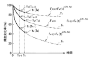
なお、各ダミー画素16の輝度は、各ダミー画素16に定電流を流し続けた場合であっても、例えば、図4に示したように、時間の経過に伴って、徐々に低下する。これは、各ダミー画素16に含まれる有機EL素子14が通電時間(発光積算時間)に応じて劣化していく性質を有しており、その劣化の進行度に応じて発光輝度が低下するからである。なお、図4中のYsは、各ダミー画素16のうち基準画素(後述)として設定された画素の初期輝度である。
Note that the luminance of each
また、各ダミー画素16の輝度劣化率の変移は一様ではない。例えば、図5に示したように、基準画素として設定された画素(ダミー画素16)の輝度劣化率を横軸にとると、基準画素の初期輝度Ysよりも小さな初期輝度のダミー画素16の輝度劣化率の変移は、当初は基準画素の輝度劣化よりも緩やかであることがわかる。一方、基準画素の初期輝度Ysよりも大きな初期輝度のダミー画素16の輝度劣化率の変移は、当初は基準画素の輝度劣化よりも急峻であることがわかる。図5に例示した各ダミー画素16の輝度劣化率の変移を式で表すと以下のようになる。

数1において、Diは、i番目のダミー画素16の輝度劣化率である。Dsは、基準画素の輝度劣化率である。n(Yi,Ys)は、基準画素の輝度に対するi番目のダミー画素16の輝度のべき係数である。べき係数n(Yi,Ys)は、例えば、以下の式に示したように、(Log(Yi(Tk))−Log(Yi(Tk-1)))を(Log(Ys(Tk))−Log(Ys(Tk-1)))で除算することにより導出される。
数2において、Log(Ys(Tk))はYs(Tk)の対数であり、Log(Ys(Tk-1))はYs(Tk-1)の対数であり、Log(Yi(Tk))はYi(Tk)の対数であり、Log(Yi(Tk-1))はYi(Tk-1)の対数である。なお、数2の右辺の分母(Log(Ys(Tk))−Log(Ys(Tk-1)))は、本発明の「第1輝度劣化情報」の一具体例に相当する。また、数2の右辺の分子(Log(Yi(Tk))−Log(Yi(Tk-1)))は、本発明の「第2輝度劣化情報」の一具体例に相当する。 In Equation 2, Log (Y s (T k )) is a logarithm of Y s (T k ), Log (Y s (T k-1 )) is a logarithm of Y s (T k-1 ), Log (Y i (T k )) is the logarithm of Y i (T k ), and Log (Y i (T k-1 )) is the logarithm of Y i (T k-1 ). The denominator (Log (Y s (T k )) − Log (Y s (T k−1 ))) on the right side of Equation 2 corresponds to a specific example of “first luminance deterioration information” of the present invention. . In addition, the numerator (Log (Y i (T k )) − Log (Y i (T k−1 ))) on the right side of Equation 2 corresponds to a specific example of “second luminance deterioration information” of the present invention. .
また、数2において、Ys(Tk)は、時刻Tkにおける基準画素の受光信号17A(輝度情報)であり、基準画素の輝度情報のうちで最新の輝度情報に相当する。また、Ys(Tk-1)は、時刻Tk-1(<時刻Tk)における基準画素の受光信号17A(輝度情報)であり、基準画素の輝度情報のうちで最新ではない輝度情報に相当する。Yi(Tk)は、時刻Tkにおけるi番目のダミー画素16の受光信号17A(輝度情報)であり、i番目のダミー画素16(非基準画素)の輝度情報のうちで最新の輝度情報に相当する。Yi(Tk-1)は、時刻Tk-1におけるi番目のダミー画素16の受光信号17A(輝度情報)であり、i番目のダミー画素16(非基準画素)の輝度情報のうちで最新ではない輝度情報に相当する。時刻Tk-1と時刻Tkとの関係は、例えば、以下の式で表される。
数3において、ΔTはサンプリング周期である。ここで、サンプリング周期ΔTとは、例えば、受光信号処理回路26が数2の右辺の分母の値および分子の値を導出する周期を指している。受光信号処理回路26は、サンプリング周期ΔTを常に一定にしている。
In Equation 3, ΔT is a sampling period. Here, the sampling period ΔT indicates, for example, a period in which the received light
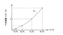
上記のようにして導出したべき係数n(Yi,Ys)は、例えば、図6に示したように、横軸を、基準画素の初期輝度Ysに対する各ダミー画素16の初期輝度Yiの割合(Yi/Ys)とすると、時刻Tkにおいて、初期輝度Yiが大きくなるにつれて大きくなる右肩上がりの曲線を描く。なお、数2からも明らかなように、べき係数n(Yi,Ys)は、Ys/Ysにおいて1である。
The coefficient n (Y i , Y s ) to be derived as described above is, for example, as shown in FIG. 6, the horizontal axis indicates the initial luminance Y i of each
次に、図7〜図13を参照して、映像信号20Aの補正に用いる補正情報26Aの導出方法について説明する。
Next, a method for deriving the
(初期設定)
まず、初期設定について説明する。受光信号処理回路26は、複数のダミー画素16のうちの一の画素を基準画素として設定する。本実施の形態では、この基準画素は、他のダミー画素16(非基準画素)に変更されることはなく、常に、同一のダミー画素16に設定される。
(Initial setting)
First, the initial setting will be described. The received light
次に、受光信号処理回路26は、時刻T1,T2において、受光素子群17から受光信号17Aを取得する。具体的には、受光信号処理回路26は、時刻T1,T2において、複数のダミー画素16のうちの一の画素である基準画素の受光信号17A(第1輝度情報)を受光素子群17から取得する。さらに、受光信号処理回路26は、時刻T1,T2において、複数のダミー画素16のうち基準画素を除く全ての画素である複数の非基準画素の受光信号17A(第2輝度情報)を受光素子群17から取得する。続いて、受光信号処理回路26は、基準画素の輝度情報から、基準画素の輝度劣化情報(Log(Ys(T2))−Log(Ys(T1)))を導出し、各非基準画素の輝度情報から、各非基準画素の輝度劣化情報(Log(Yi(T2))−Log(Yi(T1)))を導出する。
Next, the received light
次に、受光信号処理回路26は、基準画素の輝度劣化情報、および各非基準画素の輝度劣化情報から、時刻T2の時点における、基準画素の輝度情報に対する各非基準画素の輝度情報のべき係数n(Yi,Ys)を導出する。続いて、受光信号処理回路26は、基準画素の輝度情報から、時刻T2の時点における、基準画素の輝度の経時変化を表す輝度劣化関数Fs(t)(第1輝度劣化関数)を導出する。さらに、受光信号処理回路26は、輝度劣化関数Fs(t)およびべき係数n(Yi,Ys)から、時刻T2の時点における、各非基準画素の輝度の経時変化を表す輝度劣化関数Fi(t)(第2輝度劣化関数)を導出する。このようにして、受光信号処理回路26は、初期の輝度情報を用いて、時刻T2の時点における輝度劣化関数Fs(t),Fi(t)を導出する。
Next, the light reception
(データの更新)
次に、データの更新について説明する。受光信号処理回路26は、時刻Tk-1,Tkにおいて、基準画素の受光信号17A(第1輝度情報)と、複数の非基準画素の受光信号17A(第2輝度情報)を受光素子群17から取得する。このときの基準画素の受光信号17Aの値(測定値)をYs1とする(図7参照)。次に、受光信号処理回路26は、時刻Tk-1の時点における輝度劣化関数Fs(t)から、時刻Tkにおける基準画素の輝度情報を予測する。このときの予測値をYs2とする(図7参照)。続いて、受光信号処理回路26は、測定値Ys1と予測値Ys2とを比較して、測定値Ys1と予測値Ys2とが互いに一致するか否かを判定する。その結果、例えば、測定値Ys1が予測値Ys2と一致する場合には、受光信号処理回路26は、時刻Tk-1の時点における輝度劣化関数Fs(t)を、時刻Tkの時点における輝度劣化関数Fs(t)とする。一方、受光信号処理回路26は、測定値Ys1と予測値Ys2とを比較して、例えば、測定値Ys1が予測値Ys2と異なる場合には、受光信号処理回路26は、基準画素の輝度情報から、時刻Tkの時点における輝度劣化関数Fs(t)(第1輝度劣化関数)を導出する。
(Data update)
Next, data update will be described. The light reception
次に、受光信号処理回路26は、基準画素の輝度情報から、基準画素の輝度劣化情報(Log(Ys(Tk))−Log(Ys(Tk-1)))を導出する。さらに、受光信号処理回路26は、複数の非基準画素の輝度情報から、各非基準画素の輝度劣化情報(Log(Yi(Tk))−Log(Yi(Tk-1)))を導出する。次に、受光信号処理回路26は、基準画素の輝度劣化情報、および各非基準画素の輝度劣化情報から、時刻Tkの時点におけるべき係数n(Yi,Ys)を導出する。
Next, the light reception
次に、受光信号処理回路26は、時刻Tk-1の時点における輝度劣化関数Fs(t)のパラメータ(例えば、p1,p2,……,pm)を、時刻Tkの時点における輝度劣化関数Fs(t)のパラメータ(例えば、p1’,p2’,……,pm’)に更新する(図8参照)。つまり、受光信号処理回路26は、基準画素の輝度情報のうち最新の輝度情報(Ys(Tk))と、基準画素の輝度情報のうち最新ではない輝度情報(Ys(Tk-1))とに合うように、輝度劣化関数Fs(t)のパラメータを更新する。受光信号処理回路26は、例えば、新たに求めた輝度劣化関数Fs(t)のパラメータを記憶回路27に格納する。
Next, the received light
次に、受光信号処理回路26は、時刻Tkの時点における輝度劣化関数Fs(t)(図9参照)と、べき係数n(Yi,Ys)(図10参照)とから、時刻Tkの時点における輝度劣化関数Fi(t)(第2輝度劣化関数)を導出する(図11参照)。具体的には、受光信号処理回路26は、以下の式を用いて、時刻Tkの時点における輝度劣化関数Fi(t)を導出する。
次に、受光信号処理回路26は、時刻Tk-1の時点における各非基準画素の輝度劣化関数Fi(t)のパラメータを、時刻Tkの時点における各非基準画素の輝度劣化関数Fi(t)のパラメータに更新する。受光信号処理回路26は、例えば、新たに求めた輝度劣化関数Fi(t)のパラメータを記憶回路27に格納する。
Next, the received light
(輝度劣化率の予測)
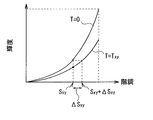
次に、受光信号処理回路26は、次のサンプリング期間が到来するまでの間、各表示画素13の輝度劣化率を予測する。具体的には、受光信号処理回路26は、輝度劣化関数Fs(t)、輝度劣化関数Fi(t)、および各表示画素13の映像信号20Aの履歴から、各表示画素13の、基準輝度における発光積算時間Txyを導出する。受光信号処理回路26は、各表示画素13の、基準輝度における発光積算時間Txyを、例えば、以下のようにして求める。
(Prediction of luminance degradation rate)
Next, the received light
図12は、各表示画素13の、基準輝度における発光積算時間Txyの導出過程を模式的に表したものである。例えば、図12に示したように、ある表示画素13の輝度が、時刻T=0〜t1の間、初期輝度Y1で発光し、時刻T=t1〜t2の間、初期輝度Y2で発光し、時刻T=t2〜t3の間、初期輝度Ynで発光したとする。このとき、この表示画素13の輝度は、厳密には、時刻T=0〜t1の間、初期輝度Y1の劣化曲線に沿って劣化し、時刻T=t1〜t2の間、初期輝度Y2の劣化曲線に沿って劣化し、時刻T=t2〜t3の間、初期輝度Ynの劣化曲線に沿って劣化する。その結果、この表示画素13の輝度は、例えば、図12に示したように48%まで劣化したとする。したがって、基準画素の輝度劣化曲線(Fs(t))において劣化率が48%となるときの時間を求めることにより、この表示画素13の、基準輝度における発光積算時間Txyを求めることができる。このように、各階調における輝度劣化曲線上を入力信号の大きさ(階調)に応じて追跡することにより、各表示画素13の、基準輝度における発光積算時間Txy、および各表示画素13の輝度劣化率を求めることができる。
FIG. 12 schematically shows a process of deriving the accumulated light emission time T xy at the reference luminance of each
(補正量の導出)
次に、受光信号処理回路26は、求めた発光積算時間Txy(または、予測した各表示画素13の輝度劣化率)と、表示パネル10ガンマ特性とから映像信号に対する補正量を導出する。受光信号処理回路26は、映像信号に対する補正量を、例えば、以下のようにして求める。
(Derivation of correction amount)
Next, the received light
図13は、T=0,Txyにおける階調(映像信号20Aの値)と輝度との関係の一例を表したものである。T=0における階調−輝度特性は、いわゆるガンマ特性と呼ばれるものである。T=Txyにおける階調−輝度特性は、ガンマ特性に対して、全階調において、輝度を48%にまで減衰させたものである。ここで、ある表示画素13において、映像信号20Aの値がSxyであったとすると、この表示画素13の輝度は、初期には、図中の白丸に対応する値となっていたことがわかる。つまり、この表示画素13の輝度は、初期から発光積算時間Txyだけ経過したときに、初期の輝度から48%にまで減衰した値となっている、と予測することができる。
FIG. 13 shows an example of the relationship between the gradation (the value of the
そこで、受光信号処理回路26は、初期から発光積算時間Txyだけ経過したときの輝度が初期の輝度と等しくなるように、映像信号20A(Sxy)に加える補正量ΔSxyを導出する。最後に、受光信号処理回路26は、補正量ΔSxyを、補正情報26Aとして記憶回路27に格納する。
Therefore, the received light
(動作・効果)
次に、本実施の形態の表示装置1の動作および効果について説明する。表示装置1に対して映像信号20Aおよび同期信号20Bが入力される。すると、信号線駆動回路23および走査線駆動回路24によって各表示画素13が駆動され、各表示画素13の映像信号20Aに応じた映像が表示領域12に表示される。さらに、ダミー画素・受光素子群駆動回路25によって各ダミー画素16が駆動されると同時に受光素子群17も駆動される。これにより、各ダミー画素16に、互いに異なる大きさの定電流が流され、その定電流の大きさに応じた輝度で各ダミー画素16が発光し、各ダミー画素16の発光光が受光素子群17で検知される。その結果、受光素子群17から、各ダミー画素16の発光光に対応する受光信号17Aが出力される。次に、受光信号処理回路26によって、以下の処理が行われる。すなわち、受光信号17Aから、基準画素の受光信号17A(輝度情報)に対する非基準画素の受光信号17A(輝度情報)のべき係数n(Yi,Ys)が導出される。次に、基準画素の輝度情報から基準画素の輝度劣化関数Fs(t)が導出されると共に、輝度劣化関数Fs(t)およびべき係数n(Yi,Ys)から非基準画素の輝度劣化関数Fi(t)が導出される。次に、輝度劣化関数Fs(t)と、輝度劣化関数Fi(t)と、各表示画素13の映像信号20Aの履歴とを利用して、各表示画素13の、基準輝度における発光積算時間Txyおよび各表示画素13の輝度劣化率が予測される。次に、初期から発光積算時間Txyだけ経過したときの輝度が初期の輝度と等しくなるように、各表示画素13の映像信号20A(Sxy)に対して補正量ΔSxyが加えられる。これにより、各表示画素13の輝度が初期の輝度となる。
(Operation / Effect)
Next, the operation and effect of the
このように、本実施の形態では、輝度劣化関数Fs(t)と、輝度劣化関数Fs(t)およびべき係数n(Yi,Ys)から得られた輝度劣化関数Fi(t)と、各表示画素13の映像信号20Aの履歴とを利用して、各表示画素13の輝度劣化率が予測される。これにより、高い精度で各表示画素13の輝度劣化を予測することができるので、各表示画素13の輝度が初期の輝度となるように、各表示画素13の映像信号20A(Sxy)に対して的確な補正量ΔSxyを加えることができる。その結果、正確に焼き付きを防止することができる。
Thus, in the present embodiment, the luminance degradation function F i (t) obtained from the luminance degradation function F s (t), the luminance degradation function F s (t), and the power coefficient n (Y i , Y s ). ) And the history of the
ところで、各表示画素13の輝度劣化率を予測する手法の1つとして、例えば、加速係数αを用いる方法がある。この方法では、まず、例えば、図14の破線に示したように、初期輝度Yiのダミー画素16の輝度劣化率が初期輝度Ysのダミー画素16の輝度劣化率と同一となるときの時間Tを求めておく。次に、例えば、図15に示したように、横軸をLog(Yi/Ys)とし、縦軸をLog(T)として、時間Tをプロットすると共に、輝度劣化率の大きさごとにプロットを直線で結んだのち、その直線の傾きを輝度劣化率の大きさごとに求める。この傾きが、上記の加速係数αとなる。続いて、例えば、図16に示したように、横軸を輝度劣化率Dとし、縦軸を加速係数αとして、加速係数αをプロットする。そして、この手法では、このプロットから、各表示画素13の輝度劣化率を予測する。具体的には、以下の式を用いて、各表示画素13の輝度劣化率を予測する。
数5において、T(Dx,Yi)は、初期輝度Yiのダミー画素16が輝度劣化率Dxに到達するまでの時間(到達時間)である。T(Dx,Ys)は、初期輝度Ysのダミー画素16が輝度劣化率Dxに到達するまでの時間(到達時間)である。α(Dx)は、輝度劣化率Dxにおける加速係数αである。
In Equation 5, T (D x , Y i ) is a time (arrival time) until the
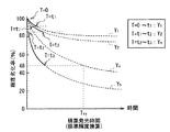
しかし、上記の手法では、以下の問題がある。例えば、図14に示したように、ある時刻Txまでは、初期輝度Yiのダミー画素16の輝度劣化率が求められているとする。このとき、初期輝度Y1のダミー画素16の輝度劣化率が80%であるとする。初期輝度Y1を除く他の初期輝度Yiのダミー画素16の輝度劣化率は、時刻Txにおいて、通常、80%よりも小さくなる。例えば、初期輝度Ysのダミー画素16の輝度劣化率は、時刻Txにおいて、65%となっており、初期輝度Ynのダミー画素16の輝度劣化率は、時刻Txにおいて、35%となっている。加速係数αは、ある劣化率に到達するのに要する時間を、初期輝度Y1〜Ynの全てのダミー画素16において求めることにより導き出される。そのため、時刻Txまでに得られた各ダミー画素16の輝度劣化率のデータでは、輝度劣化率が100%〜85%までの加速係数αしか求めることができない。その結果、輝度劣化率が85%未満のときの加速係数αについては予測するしかないので、例えば、図16に示したように、加速係数αと輝度劣化率との関係が曲線Aとなるのか、または曲線Bとなるのかは分からない場合が生じる。従って、加速係数αを用いる方法では、初期輝度Y1のダミー画素16の輝度劣化の進行具合によって、各表示画素13の輝度劣化率の予測精度が変わってしまう。もちろん、初期輝度Y1のダミー画素16の輝度劣化が進行すると、加速係数αと輝度劣化率との関係が明らかとなる。しかし、初期輝度Y1のダミー画素16の輝度劣化は、たいてい、非常に緩やかであるので、予測に必要な加速係数αと輝度劣化率との関係を得るためには、非常に長い期間の観測を必要となる。従って、加速係数αを用いる方法は、現実的ではない。
However, the above method has the following problems. For example, as shown in FIG. 14, it is assumed that the luminance deterioration rate of the
一方、本実施の形態では、観測時点のデータ(Ys(Tk)、Ys(Tk-1))で、各表示画素13の輝度劣化率を予測することができる。これにより、長時間観測をすることなく、高い精度で各表示画素の輝度劣化を予測することができる。従って、本実施の形態の予測方法は、極めて現実的である。また、本実施の形態では、観測時点のデータ(Ys(Tk)、Ys(Tk-1))で、各表示画素13の輝度劣化率を予測することができることから、更新に必要なメモリ量および計算量を小さく抑えることができる。
On the other hand, in the present embodiment, the luminance deterioration rate of each
<変形例>
上記実施の形態では、初期輝度Y1〜Ynの全てのダミー画素16が、有機EL素子14R,14G,14Bを一組とする単一の画素によって構成されていたが、初期輝度Yiの低い各ダミー画素16(低輝度画素)を複数のダミー画素(第2ダミー画素)(図示せず)によって構成してもよい。このようにした場合には、受光信号処理回路26は、複数の第2ダミー画素の輝度の平均値から、数2の右辺の分母または分子を導出することが可能である。これにより、低輝度のダミー画素16における測定誤差を小さくすることができるので、高い精度で低輝度の表示画素13の輝度劣化を予測することができる。その結果、焼き付きをより一層、正確に防止することができる。
<Modification>
In the above embodiment, all the
また、上記実施の形態では、常に特定のダミー画素16が基準画素となっていたが、必要に応じて、今まで非基準画素であったダミー画素16が基準画素となってもよい。例えば、受光信号処理回路26は、基準画素の輝度が所定の値以下となったことを検知したときには、今まで基準画素として設定されていたダミー画素16を除外すると共に複数の非基準画素のうちの一の画素を新たな基準画素に設定する。その後は、受光信号処理回路26は、今までと同様にして、数2の右辺の分母および分子を導出する。このようにした場合には、基準画素に不具合が生じた場合でも、継続して、輝度劣化を予測することができる。これにより、輝度劣化の予測の信頼性を高めることができる。
In the above embodiment, the
また、上記実施の形態では、サンプリング周期ΔTが常に一定となっていたが、可変であってもよい。例えば、受光信号処理回路26が、サンプリング周期ΔTを複数のダミー画素16の発光累積時間に応じて変化させてもよい。そのようにした場合には、例えば、発光累積時間Txyが長時間に達し、輝度劣化があまり生じなくなったときに、サンプリング周期ΔTを長くすることができる。これにより、更新に必要な計算量を小さく抑えることができる。
In the above embodiment, the sampling period ΔT is always constant, but may be variable. For example, the light reception
また、上記実施の形態では、数2を用いて、べき係数n(Yi,Ys)は導出されていたが、例えば、以下の式を用いて、べき係数n(Yi,Ys)が導出されてもよい。
数6において、右辺第2項の分母は、時刻Tkにおける基準画素の劣化速度である。右辺第2項の分子は、時刻Tkにおける非基準画素の劣化速度である。数7において、右辺第2項は、時刻Tkにおける基準画素の劣化速度を、時刻Tkにおける非基準画素の劣化速度で除算することにより得られたものである。 In Equation 6, the denominator of the second term on the right side is the deterioration rate of the reference pixel at time Tk. The numerator of the second term on the right side is the deterioration rate of the non-reference pixel at time Tk. In Equation 7, the second term on the right side is obtained by dividing the deterioration rate of the reference pixel at time Tk by the deterioration rate of the non-reference pixel at time Tk.
数6または数7を用いて、べき係数n(Yi,Ys)を導出するようにした場合には、四則演算だけで、べき係数n(Yi,Ys)を導出することができ、数2を用いたときのような対数の計算が不要である。従って、本変形例では、数2を用いてべき係数n(Yi,Ys)を導出した場合よりも、計算量を小さく抑えることができる。 Using equation 6 or C 7, exponentiation factor n (Y i, Y s) when so as to derive can be derived coefficients only four operations, exponentiation n (Y i, Y s) , The logarithmic calculation as in the case of using the equation 2 is not necessary. Therefore, in the present modification, the amount of calculation can be suppressed to be smaller than when the coefficient n (Y i , Y s ) is derived using Equation 2.
<適用例>
以下、上記実施の形態およびその変形例で説明した表示装置1の適用例について説明する。上記実施の形態等の表示装置1は、テレビジョン装置、デジタルカメラ、ノート型パーソナルコンピュータ、携帯電話等の携帯端末装置あるいはビデオカメラなど、外部から入力された映像信号あるいは内部で生成した映像信号を、画像あるいは映像として表示するあらゆる分野の電子機器の表示装置に適用することが可能である。
<Application example>
Hereinafter, application examples of the
(適用例1)
図17は、上記実施の形態等の表示装置1が適用されるテレビジョン装置の外観を表したものである。このテレビジョン装置は、例えば、フロントパネル310およびフィルターガラス320を含む映像表示画面部300を有しており、この映像表示画面部300は、上記実施の形態等の表示装置1により構成されている。
(Application example 1)
FIG. 17 illustrates an appearance of a television device to which the
(適用例2)
図18は、上記実施の形態等の表示装置1が適用されるデジタルカメラの外観を表したものである。このデジタルカメラは、例えば、フラッシュ用の発光部410、表示部420、メニュースイッチ430およびシャッターボタン440を有しており、その表示部420は、上記実施の形態等の表示装置1により構成されている。
(Application example 2)
FIG. 18 illustrates an appearance of a digital camera to which the
(適用例3)
図19は、上記実施の形態等の表示装置1が適用されるノート型パーソナルコンピュータの外観を表したものである。このノート型パーソナルコンピュータは、例えば、本体510,文字等の入力操作のためのキーボード520および画像を表示する表示部530を有しており、その表示部530は、上記実施の形態等の表示装置1により構成されている。
(Application example 3)
FIG. 19 illustrates an appearance of a notebook personal computer to which the
(適用例4)
図20は、上記実施の形態等の表示装置1が適用されるビデオカメラの外観を表したものである。このビデオカメラは、例えば、本体部610,この本体部610の前方側面に設けられた被写体撮影用のレンズ620,撮影時のスタート/ストップスイッチ630および表示部640を有しており、その表示部640は、上記実施の形態等の表示装置1により構成されている。
(Application example 4)
FIG. 20 illustrates an appearance of a video camera to which the
(適用例5)
図21は、上記実施の形態等の表示装置1が適用される携帯電話機の外観を表したものである。この携帯電話機は、例えば、上側筐体710と下側筐体720とを連結部(ヒンジ部)730で連結したものであり、ディスプレイ740,サブディスプレイ750,ピクチャーライト760およびカメラ770を有している。そのディスプレイ740またはサブディスプレイ750は、上記実施の形態等の表示装置1により構成されている。
(Application example 5)
FIG. 21 illustrates an appearance of a mobile phone to which the
1…表示装置、10…表示パネル、11,11R,11G,11B,14,14R,14G,14B…有機EL素子、12…表示領域、13…表示画素、15…非表示領域、16…ダミー画素、17…受光素子群、17A…受光信号、18…画素回路、20…駆動回路、20A,22A…映像信号、20B…同期信号、21…タイミング生成回路、21A…制御信号、22…映像信号処理回路、23…信号線駆動回路、24…走査線駆動回路、25…ダミー画素・受光素子群駆動回路、26…受光信号処理回路、26A…補正情報、27…記憶回路、30…駆動パネル、40…封止パネル、51…映像信号供給TAB、52…走査信号供給TAB、53…電源供給TCP、54…制御信号供給TCP、55…受光信号出力TCP、A,B…曲線、Cs…保持容量、D,Dx…輝度劣化率、DTL…信号線、Fi(t),Fs(t)…輝度劣化関数、GND…グラウンド線、n(Yi,Ys)…べき係数、Sxy…映像信号、T1,T2,Tx,Tk,Tk-1…時刻、Tr1…駆動トランジスタ、Tr2…書き込みトランジスタ、Txy…発光積算時間、T(Dx,Yi),T(Dx,Ys)…到達時間、Vcc…電源線、WSL…走査線、Ys1…測定値、Ys2…予測値、Y1,Y2,Yi,Ys,Yn…初期輝度、Yi(Tk),Yi(Tk-1),Ys(Tk),Ys(Tk-1)…輝度情報、α,α(Dx)…加速係数、ΔSxy…補正量、ΔT…サンプリング周期。
DESCRIPTION OF
Claims (9)
各ダミー画素に互いに異なる大きさの定電流を流して各ダミー画素を発光させる第1駆動部と、
各ダミー画素の発光光を検知して各ダミー画素の輝度情報を出力する受光部と、
前記複数のダミー画素のうちの一の画素である基準画素の第1輝度情報から前記基準画素の第1輝度劣化情報を導出すると共に、前記複数のダミー画素のうち前記基準画素を除く全ての画素である複数の非基準画素の第2輝度情報から各非基準画素の第2輝度劣化情報を導出する第1演算部と、
前記第1輝度劣化情報および前記第2輝度劣化情報から、前記第1輝度情報に対する前記第2輝度情報のべき係数を導出する第2演算部と、
前記第1輝度情報から前記基準画素の輝度の経時変化を表す第1輝度劣化関数を導出すると共に、前記第1輝度劣化関数および前記べき係数から、前記非基準画素の輝度の経時変化を表す第2輝度劣化関数を導出する第3演算部と、
前記第1輝度劣化関数、前記第2輝度劣化関数、および各表示画素の映像信号の履歴から、各表示画素の輝度劣化率を予測し、予測した各表示画素の輝度劣化率と、前記表示パネルのガンマ特性とから映像信号に対する補正量を導出する第4演算部と、
前記補正量を用いて前記映像信号を補正し、補正後の映像信号を前記複数の表示画素に出力する第2駆動部と
を備えた表示装置。 A display panel having a display area in which a plurality of display pixels are two-dimensionally arranged and a non-display area in which a plurality of dummy pixels are arranged;
A first driving unit for causing each dummy pixel to emit light by flowing constant currents of different sizes to each dummy pixel;
A light receiving unit that detects light emitted from each dummy pixel and outputs luminance information of each dummy pixel;
The first luminance deterioration information of the reference pixel is derived from the first luminance information of the reference pixel which is one pixel of the plurality of dummy pixels, and all the pixels excluding the reference pixel among the plurality of dummy pixels A first calculation unit for deriving second luminance degradation information of each non-reference pixel from second luminance information of a plurality of non-reference pixels,
A second calculation unit for deriving a power coefficient of the second luminance information with respect to the first luminance information from the first luminance deterioration information and the second luminance deterioration information;
A first luminance deterioration function that represents a change over time in the luminance of the reference pixel is derived from the first luminance information, and a first change that represents a change over time in the luminance of the non-reference pixel from the first luminance deterioration function and the power coefficient. A third calculation unit for deriving a two-luminance deterioration function ;
From the first luminance deterioration function, the second luminance deterioration function, and the video signal history of each display pixel, a luminance deterioration rate of each display pixel is predicted, the predicted luminance deterioration rate of each display pixel, and the display panel A fourth calculation unit for deriving a correction amount for the video signal from the gamma characteristic of
A display device comprising: a second drive unit that corrects the video signal using the correction amount and outputs the corrected video signal to the plurality of display pixels .
請求項1に記載の表示装置。 The third calculation unit updates the parameter of the first luminance deterioration function so as to match the latest luminance information of the first luminance information and the non-latest luminance information of the first luminance information. Item 4. The display device according to Item 1.
請求項2に記載の表示装置。 3. The parameter of the second luminance degradation function is updated from the first luminance degradation function after the parameter of the first luminance degradation function is updated and the power coefficient. Display device.
請求項1ないし請求項3のいずれか一項に記載の表示装置。 The first calculation unit is obtained by taking the logarithm of the latest luminance information of the first luminance information and the logarithm of the non-latest luminance information of the first luminance information. The first luminance deterioration information is derived by taking a difference from the obtained value, and the value obtained by taking the logarithm of the latest luminance information of the second luminance information, and the second luminance information The display device according to any one of claims 1 to 3, wherein the second luminance deterioration information is derived by taking a difference from a value obtained by taking a logarithm of luminance information that is not the latest.
請求項4に記載の表示装置。 The display device according to claim 4, wherein the second calculation unit derives the power coefficient by dividing the second luminance deterioration information by the first luminance deterioration information.
請求項1ないし請求項3のいずれか一項に記載の表示装置。 The first calculation unit derives the first luminance deterioration information by taking a difference between the latest luminance information of the first luminance information and the luminance information which is not the latest of the first luminance information, 4. The second luminance deterioration information is derived by taking a difference between the latest luminance information of the second luminance information and the non-latest luminance information of the second luminance information. 5. A display device according to claim 1.
請求項6に記載の表示装置。 The second calculation unit includes a luminance ratio obtained by dividing the latest luminance information of the second luminance information by the latest luminance information of the first luminance information, and the second luminance deterioration information. The display device according to claim 6, wherein the power coefficient is derived from a deterioration ratio obtained by dividing by the first luminance deterioration information.
請求項1ないし請求項3のいずれか一項に記載の表示装置。 4. The display device according to claim 1, wherein a period for deriving the first luminance deterioration information and the second luminance deterioration information changes according to a light emission cumulative time of the plurality of dummy pixels. 5. .
請求項1ないし請求項3のいずれか一項に記載の表示装置。 When the luminance of the reference pixel is equal to or lower than a predetermined value, the first calculation unit sets one pixel of the plurality of non-reference pixels as a new reference pixel, and the new reference pixel The first luminance degradation information is derived from the luminance information of the second non-reference pixel, and the second luminance information of all the non-reference pixels is excluded from the second luminance information of all the pixels excluding the pixel newly set as the reference pixel among the plurality of non-reference pixels. The display device according to any one of claims 1 to 3, wherein luminance degradation information is derived.
Priority Applications (5)
| Application Number | Priority Date | Filing Date | Title |
|---|---|---|---|
| JP2009217182A JP5493634B2 (en) | 2009-09-18 | 2009-09-18 | Display device |
| TW099127345A TW201207808A (en) | 2009-09-18 | 2010-08-16 | Display |
| CN201010278187.3A CN102024419B (en) | 2009-09-18 | 2010-09-10 | Display unit and brightness correction method of the same |
| US12/879,563 US20110069051A1 (en) | 2009-09-18 | 2010-09-10 | Display |
| KR1020100088765A KR20110031101A (en) | 2009-09-18 | 2010-09-10 | Display |
Applications Claiming Priority (1)
| Application Number | Priority Date | Filing Date | Title |
|---|---|---|---|
| JP2009217182A JP5493634B2 (en) | 2009-09-18 | 2009-09-18 | Display device |
Publications (3)
| Publication Number | Publication Date |
|---|---|
| JP2011065047A JP2011065047A (en) | 2011-03-31 |
| JP2011065047A5 JP2011065047A5 (en) | 2012-09-20 |
| JP5493634B2 true JP5493634B2 (en) | 2014-05-14 |
Family
ID=43756235
Family Applications (1)
| Application Number | Title | Priority Date | Filing Date |
|---|---|---|---|
| JP2009217182A Active JP5493634B2 (en) | 2009-09-18 | 2009-09-18 | Display device |
Country Status (5)
| Country | Link |
|---|---|
| US (1) | US20110069051A1 (en) |
| JP (1) | JP5493634B2 (en) |
| KR (1) | KR20110031101A (en) |
| CN (1) | CN102024419B (en) |
| TW (1) | TW201207808A (en) |
Families Citing this family (67)
| Publication number | Priority date | Publication date | Assignee | Title |
|---|---|---|---|---|
| CA2443206A1 (en) | 2003-09-23 | 2005-03-23 | Ignis Innovation Inc. | Amoled display backplanes - pixel driver circuits, array architecture, and external compensation |
| CA2472671A1 (en) | 2004-06-29 | 2005-12-29 | Ignis Innovation Inc. | Voltage-programming scheme for current-driven amoled displays |
| US10013907B2 (en) | 2004-12-15 | 2018-07-03 | Ignis Innovation Inc. | Method and system for programming, calibrating and/or compensating, and driving an LED display |
| TWI402790B (en) | 2004-12-15 | 2013-07-21 | Ignis Innovation Inc | Method and system for programming, calibrating and driving a light emitting device display |
| US9171500B2 (en) | 2011-05-20 | 2015-10-27 | Ignis Innovation Inc. | System and methods for extraction of parasitic parameters in AMOLED displays |
| US9799246B2 (en) | 2011-05-20 | 2017-10-24 | Ignis Innovation Inc. | System and methods for extraction of threshold and mobility parameters in AMOLED displays |
| US9280933B2 (en) | 2004-12-15 | 2016-03-08 | Ignis Innovation Inc. | System and methods for extraction of threshold and mobility parameters in AMOLED displays |
| US20140111567A1 (en) | 2005-04-12 | 2014-04-24 | Ignis Innovation Inc. | System and method for compensation of non-uniformities in light emitting device displays |
| US9275579B2 (en) | 2004-12-15 | 2016-03-01 | Ignis Innovation Inc. | System and methods for extraction of threshold and mobility parameters in AMOLED displays |
| US10012678B2 (en) | 2004-12-15 | 2018-07-03 | Ignis Innovation Inc. | Method and system for programming, calibrating and/or compensating, and driving an LED display |
| US8576217B2 (en) | 2011-05-20 | 2013-11-05 | Ignis Innovation Inc. | System and methods for extraction of threshold and mobility parameters in AMOLED displays |
| CA2496642A1 (en) | 2005-02-10 | 2006-08-10 | Ignis Innovation Inc. | Fast settling time driving method for organic light-emitting diode (oled) displays based on current programming |
| JP5355080B2 (en) | 2005-06-08 | 2013-11-27 | イグニス・イノベイション・インコーポレーテッド | Method and system for driving a light emitting device display |
| CA2518276A1 (en) | 2005-09-13 | 2007-03-13 | Ignis Innovation Inc. | Compensation technique for luminance degradation in electro-luminance devices |
| TW200746022A (en) | 2006-04-19 | 2007-12-16 | Ignis Innovation Inc | Stable driving scheme for active matrix displays |
| CA2556961A1 (en) | 2006-08-15 | 2008-02-15 | Ignis Innovation Inc. | Oled compensation technique based on oled capacitance |
| US9384698B2 (en) | 2009-11-30 | 2016-07-05 | Ignis Innovation Inc. | System and methods for aging compensation in AMOLED displays |
| US9311859B2 (en) | 2009-11-30 | 2016-04-12 | Ignis Innovation Inc. | Resetting cycle for aging compensation in AMOLED displays |
| CA2688870A1 (en) | 2009-11-30 | 2011-05-30 | Ignis Innovation Inc. | Methode and techniques for improving display uniformity |
| CA2669367A1 (en) | 2009-06-16 | 2010-12-16 | Ignis Innovation Inc | Compensation technique for color shift in displays |
| US10319307B2 (en) | 2009-06-16 | 2019-06-11 | Ignis Innovation Inc. | Display system with compensation techniques and/or shared level resources |
| US10867536B2 (en) | 2013-04-22 | 2020-12-15 | Ignis Innovation Inc. | Inspection system for OLED display panels |
| US10996258B2 (en) | 2009-11-30 | 2021-05-04 | Ignis Innovation Inc. | Defect detection and correction of pixel circuits for AMOLED displays |
| US8803417B2 (en) | 2009-12-01 | 2014-08-12 | Ignis Innovation Inc. | High resolution pixel architecture |
| CA2687631A1 (en) | 2009-12-06 | 2011-06-06 | Ignis Innovation Inc | Low power driving scheme for display applications |
| US9881532B2 (en) | 2010-02-04 | 2018-01-30 | Ignis Innovation Inc. | System and method for extracting correlation curves for an organic light emitting device |
| US10163401B2 (en) | 2010-02-04 | 2018-12-25 | Ignis Innovation Inc. | System and methods for extracting correlation curves for an organic light emitting device |
| CA2692097A1 (en) | 2010-02-04 | 2011-08-04 | Ignis Innovation Inc. | Extracting correlation curves for light emitting device |
| US10089921B2 (en) | 2010-02-04 | 2018-10-02 | Ignis Innovation Inc. | System and methods for extracting correlation curves for an organic light emitting device |
| US10176736B2 (en) | 2010-02-04 | 2019-01-08 | Ignis Innovation Inc. | System and methods for extracting correlation curves for an organic light emitting device |
| US20140313111A1 (en) | 2010-02-04 | 2014-10-23 | Ignis Innovation Inc. | System and methods for extracting correlation curves for an organic light emitting device |
| CA2696778A1 (en) | 2010-03-17 | 2011-09-17 | Ignis Innovation Inc. | Lifetime, uniformity, parameter extraction methods |
| US8907991B2 (en) | 2010-12-02 | 2014-12-09 | Ignis Innovation Inc. | System and methods for thermal compensation in AMOLED displays |
| US9530349B2 (en) | 2011-05-20 | 2016-12-27 | Ignis Innovations Inc. | Charged-based compensation and parameter extraction in AMOLED displays |
| US9466240B2 (en) | 2011-05-26 | 2016-10-11 | Ignis Innovation Inc. | Adaptive feedback system for compensating for aging pixel areas with enhanced estimation speed |
| JP2014517940A (en) | 2011-05-27 | 2014-07-24 | イグニス・イノベイション・インコーポレーテッド | System and method for aging compensation in AMOLED displays |
| US10089924B2 (en) | 2011-11-29 | 2018-10-02 | Ignis Innovation Inc. | Structural and low-frequency non-uniformity compensation |
| US9324268B2 (en) | 2013-03-15 | 2016-04-26 | Ignis Innovation Inc. | Amoled displays with multiple readout circuits |
| US8937632B2 (en) | 2012-02-03 | 2015-01-20 | Ignis Innovation Inc. | Driving system for active-matrix displays |
| US9747834B2 (en) | 2012-05-11 | 2017-08-29 | Ignis Innovation Inc. | Pixel circuits including feedback capacitors and reset capacitors, and display systems therefore |
| US8922544B2 (en) | 2012-05-23 | 2014-12-30 | Ignis Innovation Inc. | Display systems with compensation for line propagation delay |
| KR101972017B1 (en) * | 2012-10-31 | 2019-04-25 | 삼성디스플레이 주식회사 | Display device, apparatus for compensating degradation and method teherof |
| US9786223B2 (en) | 2012-12-11 | 2017-10-10 | Ignis Innovation Inc. | Pixel circuits for AMOLED displays |
| US9336717B2 (en) | 2012-12-11 | 2016-05-10 | Ignis Innovation Inc. | Pixel circuits for AMOLED displays |
| WO2014108879A1 (en) | 2013-01-14 | 2014-07-17 | Ignis Innovation Inc. | Driving scheme for emissive displays providing compensation for driving transistor variations |
| US9830857B2 (en) | 2013-01-14 | 2017-11-28 | Ignis Innovation Inc. | Cleaning common unwanted signals from pixel measurements in emissive displays |
| EP3043338A1 (en) | 2013-03-14 | 2016-07-13 | Ignis Innovation Inc. | Re-interpolation with edge detection for extracting an aging pattern for amoled displays |
| WO2015022626A1 (en) | 2013-08-12 | 2015-02-19 | Ignis Innovation Inc. | Compensation accuracy |
| JP6193101B2 (en) * | 2013-11-28 | 2017-09-06 | Eizo株式会社 | Prediction system, prediction method, and computer program |
| US9761170B2 (en) | 2013-12-06 | 2017-09-12 | Ignis Innovation Inc. | Correction for localized phenomena in an image array |
| US9741282B2 (en) | 2013-12-06 | 2017-08-22 | Ignis Innovation Inc. | OLED display system and method |
| US9502653B2 (en) | 2013-12-25 | 2016-11-22 | Ignis Innovation Inc. | Electrode contacts |
| DE102015206281A1 (en) | 2014-04-08 | 2015-10-08 | Ignis Innovation Inc. | Display system with shared level resources for portable devices |
| US9736906B2 (en) * | 2014-09-25 | 2017-08-15 | Intel Corporation | Control mechanism and method using RGB light emitting diodes |
| CA2879462A1 (en) | 2015-01-23 | 2016-07-23 | Ignis Innovation Inc. | Compensation for color variation in emissive devices |
| CA2889870A1 (en) | 2015-05-04 | 2016-11-04 | Ignis Innovation Inc. | Optical feedback system |
| CA2892714A1 (en) | 2015-05-27 | 2016-11-27 | Ignis Innovation Inc | Memory bandwidth reduction in compensation system |
| CA2900170A1 (en) | 2015-08-07 | 2017-02-07 | Gholamreza Chaji | Calibration of pixel based on improved reference values |
| US10323832B2 (en) | 2015-12-15 | 2019-06-18 | Wangs Alliance Corporation | LED lighting methods and apparatus |
| JP6945877B2 (en) | 2017-06-07 | 2021-10-06 | 深▲セン▼通鋭微電子技術有限公司 | Display device and image data correction method |
| CN109102758B (en) * | 2017-06-20 | 2021-08-17 | 天马微电子股份有限公司 | Display device |
| CN107342045A (en) * | 2017-08-25 | 2017-11-10 | 武汉华星光电半导体显示技术有限公司 | AMOLED display panels and display device |
| US11574979B2 (en) * | 2018-03-30 | 2023-02-07 | Sharp Kabushiki Kaisha | Display device |
| KR102617392B1 (en) * | 2019-02-20 | 2023-12-27 | 삼성디스플레이 주식회사 | Degradation compensation device and display device including the same |
| CN110364114B (en) * | 2019-07-19 | 2021-03-30 | 上海天马微电子有限公司 | Display panel, brightness compensation method thereof and display device |
| US11176859B2 (en) * | 2020-03-24 | 2021-11-16 | Synaptics Incorporated | Device and method for display module calibration |
| CN114927550B (en) | 2022-05-26 | 2023-06-09 | 惠科股份有限公司 | Display panel and display device |
Family Cites Families (10)
| Publication number | Priority date | Publication date | Assignee | Title |
|---|---|---|---|---|
| US6552735B1 (en) * | 2000-09-01 | 2003-04-22 | Rockwell Collins, Inc. | Method for eliminating latent images on display devices |
| US6320325B1 (en) * | 2000-11-06 | 2001-11-20 | Eastman Kodak Company | Emissive display with luminance feedback from a representative pixel |
| GB0424112D0 (en) * | 2004-10-29 | 2004-12-01 | Koninkl Philips Electronics Nv | Active matrix display devices |
| CN100483486C (en) * | 2005-01-27 | 2009-04-29 | 友达光电股份有限公司 | Display device and used display panel, pixel circuit and compensating mechanism |
| JP2007156044A (en) * | 2005-12-05 | 2007-06-21 | Sony Corp | Spontaneous light emission display device, gray scale value/deterioration rate conversion table update device, and program |
| JP5124939B2 (en) * | 2005-12-21 | 2013-01-23 | ソニー株式会社 | Self-luminous display device, conversion table update device, and program |
| JP5130634B2 (en) * | 2006-03-08 | 2013-01-30 | ソニー株式会社 | Self-luminous display device, electronic device, burn-in correction device, and program |
| JP5171329B2 (en) * | 2007-09-28 | 2013-03-27 | 株式会社ジャパンディスプレイウェスト | Display device |
| KR100902238B1 (en) * | 2008-01-18 | 2009-06-11 | 삼성모바일디스플레이주식회사 | Organic light emitting display and driving method thereof |
| JP5246433B2 (en) * | 2009-09-18 | 2013-07-24 | ソニー株式会社 | Display device |
-
2009
- 2009-09-18 JP JP2009217182A patent/JP5493634B2/en active Active
-
2010
- 2010-08-16 TW TW099127345A patent/TW201207808A/en unknown
- 2010-09-10 KR KR1020100088765A patent/KR20110031101A/en not_active Application Discontinuation
- 2010-09-10 CN CN201010278187.3A patent/CN102024419B/en not_active Expired - Fee Related
- 2010-09-10 US US12/879,563 patent/US20110069051A1/en not_active Abandoned
Also Published As
| Publication number | Publication date |
|---|---|
| CN102024419B (en) | 2013-08-14 |
| KR20110031101A (en) | 2011-03-24 |
| TW201207808A (en) | 2012-02-16 |
| US20110069051A1 (en) | 2011-03-24 |
| JP2011065047A (en) | 2011-03-31 |
| CN102024419A (en) | 2011-04-20 |
Similar Documents
| Publication | Publication Date | Title |
|---|---|---|
| JP5493634B2 (en) | Display device | |
| JP5246433B2 (en) | Display device | |
| TWI598866B (en) | A data processing device for a display device, a data processing method for the display device and the display device | |
| AU2008254180B2 (en) | Display device, display device drive method, and computer program | |
| JP5010949B2 (en) | Organic EL display device | |
| JP4572523B2 (en) | Pixel circuit driving method, driving circuit, electro-optical device, and electronic apparatus | |
| US8330682B2 (en) | Display apparatus, display control apparatus, and display control method as well as program | |
| US11238793B2 (en) | Pixel compensation method and system, display device | |
| JP2011065048A5 (en) | ||
| TWI409756B (en) | Display device, method for driving same, and electronic apparatus | |
| US8154566B2 (en) | Active-matrix display apparatus driving method of the same and electronic instruments | |
| JP2008176115A (en) | Display apparatus, control computation unit, and display driving method | |
| US9001099B2 (en) | Image display and image display method | |
| JP2008241782A (en) | Display device and driving method thereof and electronic equipment | |
| JP2011082213A (en) | Display panel, module, and electronic apparatus | |
| KR102505891B1 (en) | Organic Light Emitting Display Device and Method of Driving the same | |
| JP2008197607A (en) | Pixel circuit, image display device and its driving method | |
| JP2013057726A (en) | Display panel, display device and, electronic device | |
| JP2011128443A (en) | Display device, method of driving the same, and electronic equipment | |
| JP2011070018A (en) | Display device | |
| JP2010039117A (en) | Display, its driving method, and electronic device | |
| JP2010096908A (en) | Display | |
| US20230386390A1 (en) | Display Device and Display Driving Method | |
| JP2009103871A (en) | Display device, driving method therefor and electronic equipment | |
| CN117238251A (en) | Display panel, driving method thereof and display device |
Legal Events
| Date | Code | Title | Description |
|---|---|---|---|
| A521 | Request for written amendment filed |
Free format text: JAPANESE INTERMEDIATE CODE: A523 Effective date: 20120803 |
|
| A621 | Written request for application examination |
Free format text: JAPANESE INTERMEDIATE CODE: A621 Effective date: 20120803 |
|
| A977 | Report on retrieval |
Free format text: JAPANESE INTERMEDIATE CODE: A971007 Effective date: 20130313 |
|
| A131 | Notification of reasons for refusal |
Free format text: JAPANESE INTERMEDIATE CODE: A131 Effective date: 20130502 |
|
| A521 | Request for written amendment filed |
Free format text: JAPANESE INTERMEDIATE CODE: A523 Effective date: 20130619 |
|
| TRDD | Decision of grant or rejection written | ||
| A01 | Written decision to grant a patent or to grant a registration (utility model) |
Free format text: JAPANESE INTERMEDIATE CODE: A01 Effective date: 20140204 |
|
| A61 | First payment of annual fees (during grant procedure) |
Free format text: JAPANESE INTERMEDIATE CODE: A61 Effective date: 20140217 |
|
| R151 | Written notification of patent or utility model registration |
Ref document number: 5493634 Country of ref document: JP Free format text: JAPANESE INTERMEDIATE CODE: R151 |
|
| S111 | Request for change of ownership or part of ownership |
Free format text: JAPANESE INTERMEDIATE CODE: R313111 |
|
| R350 | Written notification of registration of transfer |
Free format text: JAPANESE INTERMEDIATE CODE: R350 |
|
| R250 | Receipt of annual fees |
Free format text: JAPANESE INTERMEDIATE CODE: R250 |
|
| R250 | Receipt of annual fees |
Free format text: JAPANESE INTERMEDIATE CODE: R250 |
|
| R250 | Receipt of annual fees |
Free format text: JAPANESE INTERMEDIATE CODE: R250 |
|
| R250 | Receipt of annual fees |
Free format text: JAPANESE INTERMEDIATE CODE: R250 |
|
| R250 | Receipt of annual fees |
Free format text: JAPANESE INTERMEDIATE CODE: R250 |
|
| R250 | Receipt of annual fees |
Free format text: JAPANESE INTERMEDIATE CODE: R250 |
|
| S303 | Written request for registration of pledge or change of pledge |
Free format text: JAPANESE INTERMEDIATE CODE: R316303 |
|
| R350 | Written notification of registration of transfer |
Free format text: JAPANESE INTERMEDIATE CODE: R350 |
|
| R250 | Receipt of annual fees |
Free format text: JAPANESE INTERMEDIATE CODE: R250 |
|
| S803 | Written request for registration of cancellation of provisional registration |
Free format text: JAPANESE INTERMEDIATE CODE: R316803 |
|
| R350 | Written notification of registration of transfer |
Free format text: JAPANESE INTERMEDIATE CODE: R350 |
|
| R250 | Receipt of annual fees |
Free format text: JAPANESE INTERMEDIATE CODE: R250 |
|
| S111 | Request for change of ownership or part of ownership |
Free format text: JAPANESE INTERMEDIATE CODE: R313113 |