JP5482393B2 - Display device, display device layout method, and electronic apparatus - Google Patents
Display device, display device layout method, and electronic apparatus Download PDFInfo
- Publication number
- JP5482393B2 JP5482393B2 JP2010089803A JP2010089803A JP5482393B2 JP 5482393 B2 JP5482393 B2 JP 5482393B2 JP 2010089803 A JP2010089803 A JP 2010089803A JP 2010089803 A JP2010089803 A JP 2010089803A JP 5482393 B2 JP5482393 B2 JP 5482393B2
- Authority
- JP
- Japan
- Prior art keywords
- pixel
- signal
- signal lines
- display device
- display
- Prior art date
- Legal status (The legal status is an assumption and is not a legal conclusion. Google has not performed a legal analysis and makes no representation as to the accuracy of the status listed.)
- Expired - Fee Related
Links
Images


Classifications
-
- G—PHYSICS
- G09—EDUCATION; CRYPTOGRAPHY; DISPLAY; ADVERTISING; SEALS
- G09G—ARRANGEMENTS OR CIRCUITS FOR CONTROL OF INDICATING DEVICES USING STATIC MEANS TO PRESENT VARIABLE INFORMATION
- G09G3/00—Control arrangements or circuits, of interest only in connection with visual indicators other than cathode-ray tubes
- G09G3/20—Control arrangements or circuits, of interest only in connection with visual indicators other than cathode-ray tubes for presentation of an assembly of a number of characters, e.g. a page, by composing the assembly by combination of individual elements arranged in a matrix no fixed position being assigned to or needed to be assigned to the individual characters or partial characters
- G09G3/34—Control arrangements or circuits, of interest only in connection with visual indicators other than cathode-ray tubes for presentation of an assembly of a number of characters, e.g. a page, by composing the assembly by combination of individual elements arranged in a matrix no fixed position being assigned to or needed to be assigned to the individual characters or partial characters by control of light from an independent source
- G09G3/36—Control arrangements or circuits, of interest only in connection with visual indicators other than cathode-ray tubes for presentation of an assembly of a number of characters, e.g. a page, by composing the assembly by combination of individual elements arranged in a matrix no fixed position being assigned to or needed to be assigned to the individual characters or partial characters by control of light from an independent source using liquid crystals
- G09G3/3611—Control of matrices with row and column drivers
-
- G—PHYSICS
- G09—EDUCATION; CRYPTOGRAPHY; DISPLAY; ADVERTISING; SEALS
- G09G—ARRANGEMENTS OR CIRCUITS FOR CONTROL OF INDICATING DEVICES USING STATIC MEANS TO PRESENT VARIABLE INFORMATION
- G09G3/00—Control arrangements or circuits, of interest only in connection with visual indicators other than cathode-ray tubes
- G09G3/20—Control arrangements or circuits, of interest only in connection with visual indicators other than cathode-ray tubes for presentation of an assembly of a number of characters, e.g. a page, by composing the assembly by combination of individual elements arranged in a matrix no fixed position being assigned to or needed to be assigned to the individual characters or partial characters
- G09G3/22—Control arrangements or circuits, of interest only in connection with visual indicators other than cathode-ray tubes for presentation of an assembly of a number of characters, e.g. a page, by composing the assembly by combination of individual elements arranged in a matrix no fixed position being assigned to or needed to be assigned to the individual characters or partial characters using controlled light sources
- G09G3/30—Control arrangements or circuits, of interest only in connection with visual indicators other than cathode-ray tubes for presentation of an assembly of a number of characters, e.g. a page, by composing the assembly by combination of individual elements arranged in a matrix no fixed position being assigned to or needed to be assigned to the individual characters or partial characters using controlled light sources using electroluminescent panels
- G09G3/32—Control arrangements or circuits, of interest only in connection with visual indicators other than cathode-ray tubes for presentation of an assembly of a number of characters, e.g. a page, by composing the assembly by combination of individual elements arranged in a matrix no fixed position being assigned to or needed to be assigned to the individual characters or partial characters using controlled light sources using electroluminescent panels semiconductive, e.g. using light-emitting diodes [LED]
- G09G3/3208—Control arrangements or circuits, of interest only in connection with visual indicators other than cathode-ray tubes for presentation of an assembly of a number of characters, e.g. a page, by composing the assembly by combination of individual elements arranged in a matrix no fixed position being assigned to or needed to be assigned to the individual characters or partial characters using controlled light sources using electroluminescent panels semiconductive, e.g. using light-emitting diodes [LED] organic, e.g. using organic light-emitting diodes [OLED]
- G09G3/3225—Control arrangements or circuits, of interest only in connection with visual indicators other than cathode-ray tubes for presentation of an assembly of a number of characters, e.g. a page, by composing the assembly by combination of individual elements arranged in a matrix no fixed position being assigned to or needed to be assigned to the individual characters or partial characters using controlled light sources using electroluminescent panels semiconductive, e.g. using light-emitting diodes [LED] organic, e.g. using organic light-emitting diodes [OLED] using an active matrix
- G09G3/3233—Control arrangements or circuits, of interest only in connection with visual indicators other than cathode-ray tubes for presentation of an assembly of a number of characters, e.g. a page, by composing the assembly by combination of individual elements arranged in a matrix no fixed position being assigned to or needed to be assigned to the individual characters or partial characters using controlled light sources using electroluminescent panels semiconductive, e.g. using light-emitting diodes [LED] organic, e.g. using organic light-emitting diodes [OLED] using an active matrix with pixel circuitry controlling the current through the light-emitting element
-
- G—PHYSICS
- G09—EDUCATION; CRYPTOGRAPHY; DISPLAY; ADVERTISING; SEALS
- G09G—ARRANGEMENTS OR CIRCUITS FOR CONTROL OF INDICATING DEVICES USING STATIC MEANS TO PRESENT VARIABLE INFORMATION
- G09G3/00—Control arrangements or circuits, of interest only in connection with visual indicators other than cathode-ray tubes
- G09G3/20—Control arrangements or circuits, of interest only in connection with visual indicators other than cathode-ray tubes for presentation of an assembly of a number of characters, e.g. a page, by composing the assembly by combination of individual elements arranged in a matrix no fixed position being assigned to or needed to be assigned to the individual characters or partial characters
- G09G3/22—Control arrangements or circuits, of interest only in connection with visual indicators other than cathode-ray tubes for presentation of an assembly of a number of characters, e.g. a page, by composing the assembly by combination of individual elements arranged in a matrix no fixed position being assigned to or needed to be assigned to the individual characters or partial characters using controlled light sources
- G09G3/30—Control arrangements or circuits, of interest only in connection with visual indicators other than cathode-ray tubes for presentation of an assembly of a number of characters, e.g. a page, by composing the assembly by combination of individual elements arranged in a matrix no fixed position being assigned to or needed to be assigned to the individual characters or partial characters using controlled light sources using electroluminescent panels
- G09G3/32—Control arrangements or circuits, of interest only in connection with visual indicators other than cathode-ray tubes for presentation of an assembly of a number of characters, e.g. a page, by composing the assembly by combination of individual elements arranged in a matrix no fixed position being assigned to or needed to be assigned to the individual characters or partial characters using controlled light sources using electroluminescent panels semiconductive, e.g. using light-emitting diodes [LED]
- G09G3/3208—Control arrangements or circuits, of interest only in connection with visual indicators other than cathode-ray tubes for presentation of an assembly of a number of characters, e.g. a page, by composing the assembly by combination of individual elements arranged in a matrix no fixed position being assigned to or needed to be assigned to the individual characters or partial characters using controlled light sources using electroluminescent panels semiconductive, e.g. using light-emitting diodes [LED] organic, e.g. using organic light-emitting diodes [OLED]
- G09G3/3275—Details of drivers for data electrodes
- G09G3/3291—Details of drivers for data electrodes in which the data driver supplies a variable data voltage for setting the current through, or the voltage across, the light-emitting elements
-
- G—PHYSICS
- G09—EDUCATION; CRYPTOGRAPHY; DISPLAY; ADVERTISING; SEALS
- G09G—ARRANGEMENTS OR CIRCUITS FOR CONTROL OF INDICATING DEVICES USING STATIC MEANS TO PRESENT VARIABLE INFORMATION
- G09G2300/00—Aspects of the constitution of display devices
- G09G2300/04—Structural and physical details of display devices
- G09G2300/0421—Structural details of the set of electrodes
- G09G2300/0426—Layout of electrodes and connections
-
- G—PHYSICS
- G09—EDUCATION; CRYPTOGRAPHY; DISPLAY; ADVERTISING; SEALS
- G09G—ARRANGEMENTS OR CIRCUITS FOR CONTROL OF INDICATING DEVICES USING STATIC MEANS TO PRESENT VARIABLE INFORMATION
- G09G2300/00—Aspects of the constitution of display devices
- G09G2300/08—Active matrix structure, i.e. with use of active elements, inclusive of non-linear two terminal elements, in the pixels together with light emitting or modulating elements
- G09G2300/0809—Several active elements per pixel in active matrix panels
- G09G2300/0819—Several active elements per pixel in active matrix panels used for counteracting undesired variations, e.g. feedback or autozeroing
-
- G—PHYSICS
- G09—EDUCATION; CRYPTOGRAPHY; DISPLAY; ADVERTISING; SEALS
- G09G—ARRANGEMENTS OR CIRCUITS FOR CONTROL OF INDICATING DEVICES USING STATIC MEANS TO PRESENT VARIABLE INFORMATION
- G09G2300/00—Aspects of the constitution of display devices
- G09G2300/08—Active matrix structure, i.e. with use of active elements, inclusive of non-linear two terminal elements, in the pixels together with light emitting or modulating elements
- G09G2300/0809—Several active elements per pixel in active matrix panels
- G09G2300/0842—Several active elements per pixel in active matrix panels forming a memory circuit, e.g. a dynamic memory with one capacitor
- G09G2300/0861—Several active elements per pixel in active matrix panels forming a memory circuit, e.g. a dynamic memory with one capacitor with additional control of the display period without amending the charge stored in a pixel memory, e.g. by means of additional select electrodes
- G09G2300/0866—Several active elements per pixel in active matrix panels forming a memory circuit, e.g. a dynamic memory with one capacitor with additional control of the display period without amending the charge stored in a pixel memory, e.g. by means of additional select electrodes by means of changes in the pixel supply voltage
-
- G—PHYSICS
- G09—EDUCATION; CRYPTOGRAPHY; DISPLAY; ADVERTISING; SEALS
- G09G—ARRANGEMENTS OR CIRCUITS FOR CONTROL OF INDICATING DEVICES USING STATIC MEANS TO PRESENT VARIABLE INFORMATION
- G09G2310/00—Command of the display device
- G09G2310/02—Addressing, scanning or driving the display screen or processing steps related thereto
- G09G2310/0243—Details of the generation of driving signals
- G09G2310/0254—Control of polarity reversal in general, other than for liquid crystal displays
-
- G—PHYSICS
- G09—EDUCATION; CRYPTOGRAPHY; DISPLAY; ADVERTISING; SEALS
- G09G—ARRANGEMENTS OR CIRCUITS FOR CONTROL OF INDICATING DEVICES USING STATIC MEANS TO PRESENT VARIABLE INFORMATION
- G09G2310/00—Command of the display device
- G09G2310/02—Addressing, scanning or driving the display screen or processing steps related thereto
- G09G2310/0264—Details of driving circuits
- G09G2310/0297—Special arrangements with multiplexing or demultiplexing of display data in the drivers for data electrodes, in a pre-processing circuitry delivering display data to said drivers or in the matrix panel, e.g. multiplexing plural data signals to one D/A converter or demultiplexing the D/A converter output to multiple columns
-
- G—PHYSICS
- G09—EDUCATION; CRYPTOGRAPHY; DISPLAY; ADVERTISING; SEALS
- G09G—ARRANGEMENTS OR CIRCUITS FOR CONTROL OF INDICATING DEVICES USING STATIC MEANS TO PRESENT VARIABLE INFORMATION
- G09G2310/00—Command of the display device
- G09G2310/06—Details of flat display driving waveforms
- G09G2310/061—Details of flat display driving waveforms for resetting or blanking
-
- G—PHYSICS
- G09—EDUCATION; CRYPTOGRAPHY; DISPLAY; ADVERTISING; SEALS
- G09G—ARRANGEMENTS OR CIRCUITS FOR CONTROL OF INDICATING DEVICES USING STATIC MEANS TO PRESENT VARIABLE INFORMATION
- G09G2320/00—Control of display operating conditions
- G09G2320/02—Improving the quality of display appearance
- G09G2320/0209—Crosstalk reduction, i.e. to reduce direct or indirect influences of signals directed to a certain pixel of the displayed image on other pixels of said image, inclusive of influences affecting pixels in different frames or fields or sub-images which constitute a same image, e.g. left and right images of a stereoscopic display
Landscapes
- Engineering & Computer Science (AREA)
- Physics & Mathematics (AREA)
- Computer Hardware Design (AREA)
- General Physics & Mathematics (AREA)
- Theoretical Computer Science (AREA)
- Chemical & Material Sciences (AREA)
- Crystallography & Structural Chemistry (AREA)
- Control Of Indicators Other Than Cathode Ray Tubes (AREA)
- Control Of El Displays (AREA)
- Electroluminescent Light Sources (AREA)
- Devices For Indicating Variable Information By Combining Individual Elements (AREA)
Description
本発明は、表示装置、表示装置のレイアウト方法、及び、電子機器に関し、特に、発光部を含む画素回路が行列状(マトリクス状)に2次元配列されてなる平面型の表示装置、当該表示装置のレイアウト方法、及び、当該表示装置を有する電子機器に関する。 The present invention relates to a display device, a display device layout method, and an electronic apparatus, and in particular, a planar display device in which pixel circuits including light emitting units are two-dimensionally arranged in a matrix (matrix shape), and the display device And an electronic apparatus having the display device.
近年、画像表示を行う表示装置の分野では、画素回路(以下、単に「画素」と記述する場合もある)が行列状に配列(配置)されてなる平面型(フラットパネル型)の表示装置が急速に普及している。平面型の表示装置の一つとして、デバイスに流れる電流値に応じて発光輝度が変化する、所謂電流駆動型の電気光学素子を画素の発光部(発光素子)として用いた表示装置がある。電流駆動型の電気光学素子としては、有機材料のエレクトロルミネッセンス(Electroluminescence;EL)を利用し、有機薄膜に電界をかけると発光する現象を用いた有機EL素子が知られている。 2. Description of the Related Art In recent years, in the field of display devices that perform image display, planar (flat panel) display devices in which pixel circuits (hereinafter sometimes simply referred to as “pixels”) are arranged (arranged) in a matrix form are known. It is rapidly spreading. As one of flat-type display devices, there is a display device using a so-called current-driven electro-optic element whose light emission luminance changes according to a current value flowing through the device as a light emitting portion (light emitting element) of a pixel. As a current-driven electro-optical element, an organic EL element using a phenomenon that emits light when an electric field is applied to an organic thin film is known using electroluminescence (EL) of an organic material.
画素の発光部として有機EL素子を用いた有機EL表示装置は次のような特長を持っている。すなわち、有機EL素子は、10V以下の印加電圧で駆動できるために低消費電力である。有機EL素子は、自発光素子であるために液晶表示装置に比べて、画像の視認性が高く、しかもバックライト等の照明部材を必要としないために軽量化及び薄型化が容易である。更に、有機EL素子は、応答速度が数μsec程度と非常に高速であるために動画表示時の残像が発生しない。 An organic EL display device using an organic EL element as a light emitting portion of a pixel has the following features. That is, since the organic EL element can be driven with an applied voltage of 10 V or less, the power consumption is low. Since the organic EL element is a self-luminous element, the image visibility is higher than that of the liquid crystal display device, and it does not require an illumination member such as a backlight. Therefore, the organic EL element can be easily reduced in weight and thickness. Furthermore, since the organic EL element has a very high response speed of about several μsec, an afterimage does not occur when displaying a moving image.
有機EL表示装置や液晶表示装置等の平面型表示装置では、その駆動方式としてパッシブマトリクス方式とアクティブマトリクス方式とを採ることができる。これらの方式のうち、アクティブマトリクス方式の表示装置は、電気光学素子が1表示フレームの期間に亘って発光を持続するために、大型でかつ高精細な表示装置の実現が容易である。このアクティブマトリクス方式の表示装置では、電気光学素子に流れる電流を、当該電気光学素子と同じ画素内に設けた能動素子、例えば絶縁ゲート型電界効果トランジスタによって制御する。絶縁ゲート型電界効果トランジスタとしては、一般には、TFT(Thin Film Transistor;薄膜トランジスタ)が用いられる。 In a flat display device such as an organic EL display device and a liquid crystal display device, a passive matrix method and an active matrix method can be adopted as the driving method. Among these methods, an active matrix display device can easily realize a large-sized and high-definition display device because the electro-optic element continues to emit light for a period of one display frame. In this active matrix display device, the current flowing through the electro-optical element is controlled by an active element, for example, an insulated gate field effect transistor, provided in the same pixel as the electro-optical element. As the insulated gate field effect transistor, a TFT (Thin Film Transistor) is generally used.
ところで、有機EL表示装置や液晶表示装置等の平面型表示装置では、画素が行列状に配列されてなる画素アレイ部において、隣接する2つの画素列に属する画素回路に接続される2つの信号線を隣接して配線するレイアウト構造を採る場合がある。この種のレイアウト構造として、例えば、行列状の画素配列の列方向の軸を挟んで隣接する奇数列の画素回路と偶数列の画素回路とを、当該列方向の軸に関して対称にレイアウトする構造が知られている。 By the way, in a flat display device such as an organic EL display device or a liquid crystal display device, two signal lines connected to pixel circuits belonging to two adjacent pixel columns in a pixel array section in which pixels are arranged in a matrix. In some cases, a layout structure is used in which wiring is adjacent to each other. As this type of layout structure, for example, there is a structure in which pixel circuits in odd-numbered columns and pixel circuits in even-numbered columns adjacent to each other across the column-direction axis of a matrix-like pixel arrangement are laid out symmetrically with respect to the column-direction axis. Are known.
以下では、列方向の軸を挟んで隣接する奇数列の画素回路と偶数列の画素回路とを、当該列方向の軸に関して対称にレイアウトする構造をミラー型レイアウト構造と呼ぶこととする。このミラー型レイアウト構造によれば、画素アレイ部の効率的なレイアウトが可能になるとともに、レイアウトの自由度が上がる等のメリットがある。 Hereinafter, a structure in which pixel circuits in odd-numbered columns and pixel circuits in even-numbered columns that are adjacent to each other with the axis in the column direction being laid out symmetrically with respect to the axis in the column direction is referred to as a mirror layout structure. According to this mirror type layout structure, there is an advantage that an efficient layout of the pixel array portion is possible and the degree of freedom of layout is increased.
ここで、ミラー型レイアウト構造を採った場合、列方向に沿う信号線が奇数列と偶数列の画素回路間で隣接することがある。従って、隣接する信号線間に寄生容量が存在しないようにするために、隣接する信号線間にシールド線を配線するようにしている(例えば、特許文献1を参照)。 Here, when taking a mirror type layout structure, it may signal lines along the column direction are adjacent between pixel circuits of the odd columns and even columns. Therefore, in order to prevent parasitic capacitance from existing between adjacent signal lines, a shield line is provided between adjacent signal lines (see, for example, Patent Document 1).
一方で、有機EL表示装置や液晶表示装置等の平面型表示装置において、表示パネルに対して表示パネルの外部から表示信号を供給する駆動部の出力数の削減を図るために、所謂セレクタ駆動方式が採用されている(例えば、特許文献2を参照)。このセレクタ駆動方式は、時(時間)分割駆動方式と呼ばれることもある。 On the other hand, in a flat display device such as an organic EL display device or a liquid crystal display device, a so-called selector drive system is used to reduce the number of outputs of a drive unit that supplies a display signal to the display panel from the outside of the display panel. Is employed (see, for example, Patent Document 2). This selector driving method is sometimes called a time (time) division driving method.
セレクタ駆動方式では、表示パネル外の駆動部の1つの出力に対して、表示パネル上の複数の信号線を単位(組)として割り当て、駆動部から時系列で出力される表示信号を、セレクタ回路で複数の信号線に対して時間分割的(時分割)に分配する駆動が行われる。このセレクタ駆動方式によれば、単位となる信号線の本数を例えば3本とした場合、表示パネル上の信号線の総数に対して、表示パネル外の駆動部の出力数を1/3にできるメリットがある。 The selector driving method, with respect to one output of the drive unit outside the display panel, assigns the multiple signal lines on the display panel units (set), the display signal outputted in time series from the drive unit, the selector The circuit is driven to distribute a plurality of signal lines in a time division manner (time division). According to this selector driving method, when the number of signal lines as a unit is, for example, three, the number of outputs of the driving unit outside the display panel can be reduced to 1/3 with respect to the total number of signal lines on the display panel. There are benefits.
特許文献1に記載の従来技術は、隣接する信号線間にシールド線を配線することで、隣接する信号線間に寄生容量が存在しないようにできるものの、信号線の他にシールド線を配線することになるため、必ずしも最適な手法であるとは言えない。具体的には、シールド線はそもそも画素回路の駆動には本来不要な配線であり、画素配列における配線数を増やすことになるため、配線のレイアウトに制約を与えることになる。
Although the prior art described in
また、一方で、ミラー型レイアウト構造とセレクタ駆動方式とを併用する場合、隣接する2つの信号線間に寄生容量が存在していると、当該2つの信号線に対するセレクタ回路の選択タイミングが異なると不具合が生じる。具体的には、先に信号線に書き込まれた表示信号が、後に信号線に書き込まれる表示信号の影響を受けるため、正確な表示信号を書き込むことができない(その詳細については後述する)。正確な表示信号を信号線に書き込めないと、表示画像の画質の劣化を招くことになる。 On the other hand, when the mirror type layout structure and the selector driving method are used in combination, if there is a parasitic capacitance between two adjacent signal lines, the selection timing of the selector circuit for the two signal lines is different. A malfunction occurs. Specifically, an accurate display signal cannot be written because a display signal previously written to the signal line is affected by a display signal written to the signal line later (details thereof will be described later). If an accurate display signal cannot be written to the signal line, the image quality of the display image is deteriorated.
ここでは、ミラー型レイアウト構造とセレクタ駆動方式とを併用する場合の不具合について述べたが、セレクタ駆動方式単独の場合であっても、隣接する2つの信号線に対する表示信号の書込みのタイミングが異なっていると同様の不具合が発生することになる。 Here, the problem in the case where the mirror type layout structure and the selector driving method are used together has been described. However, even in the case of the selector driving method alone, the timing of writing display signals to two adjacent signal lines differs. If this happens, the same problem will occur.
そこで、本発明は、隣接する2つの画素列に属する画素回路に接続される2つの信号線に対する表示信号の書込みのタイミングが異なっても、正確な表示信号の書込みが可能な表示装置、表示装置のレイアウト方法、及び、電子機器を提供することを目的とする。 Accordingly, the present invention provides a display device and a display device capable of accurately writing a display signal even when display signal write timings for two signal lines connected to pixel circuits belonging to two adjacent pixel columns are different. An object of the present invention is to provide a layout method and an electronic device.
上記目的を達成するために、本発明は、
発光部を含む画素回路が行列状に配列されてなる画素アレイ部と、
前記画素回路の行列状の配列に対して画素列毎に配線され、各画素列に属する画素回路に接続される信号線と、
1つの入力信号線から時系列に与えられる表示信号を、複数の信号線に対して時間分割的に分配するセレクタ回路と
を備える表示装置において、
前記信号線をレイアウトするに当たって、
隣接する2つの画素列に属する画素回路にそれぞれ接続される2つの信号線の組み合わせにおいて、
前記セレクタ回路によって異なるタイミングで表示信号が分配される組み合わせについては2つの信号線を隣接しないように配線し、
前記セレクタ回路によって同一のタイミングで表示信号が分配される組み合わせについては2つの信号線を隣接して配線する
構成を採る。
In order to achieve the above object, the present invention provides:
A pixel array unit in which pixel circuits including light emitting units are arranged in a matrix;
A signal line wired for each pixel column to the matrix arrangement of the pixel circuits and connected to the pixel circuits belonging to each pixel column;
In a display device comprising a selector circuit that time-divisionally distributes a display signal given in time series from one input signal line to a plurality of signal lines,
In laying out the signal lines,
In a combination of two signal lines respectively connected to pixel circuits belonging to two adjacent pixel columns,
For combinations in which display signals are distributed at different timings by the selector circuit, two signal lines are wired so as not to be adjacent,
For a combination in which display signals are distributed at the same timing by the selector circuit, two signal lines are arranged adjacent to each other.
隣接する2つの画素列に属する画素回路にそれぞれ接続される2つの信号線の組み合わせにおいて、セレクタ回路によって異なるタイミングで表示信号が分配される組み合わせについては、2つの信号線が隣接していないことで、当該2つの信号線間には寄生容量が存在しない。従って、2つの信号線に対して異なるタイミングで表示信号が書き込まれても、先に信号線に書き込まれた表示信号が、後に信号線に書き込まれる表示信号の影響を受けることはない。また、セレクタ回路によって同一のタイミングで表示信号が分配される組み合わせについては、2つの信号線が隣接していることで、当該2つの信号線間には寄生容量が存在することになる。しかし、寄生容量が存在していても、2つの信号線に対して表示信号が同一タイミングで書き込まれるため、相互に相手方の表示信号の影響を受けることはない。従って、2つの信号線の組み合わせのいずれの場合にも、信号線に対する正確な表示信号の書込みが可能になる。 In a combination of two signal lines respectively connected to pixel circuits belonging to two adjacent pixel columns, the display signal is distributed at different timings by the selector circuit, because the two signal lines are not adjacent to each other. There is no parasitic capacitance between the two signal lines. Therefore, even if display signals are written to the two signal lines at different timings, the display signals written to the signal lines first are not affected by the display signals written to the signal lines later. In addition, in the combination in which the display signal is distributed at the same timing by the selector circuit, since the two signal lines are adjacent to each other, there is a parasitic capacitance between the two signal lines. However, even if there is a parasitic capacitance, the display signals are written to the two signal lines at the same timing, so that they are not affected by the display signals of the other party. Therefore, in any case of the combination of the two signal lines, the display signal can be accurately written to the signal lines.
本発明によれば、隣接する2つの画素列の各信号線に対する表示信号の書込みのタイミングが異なっても、正確な表示信号を信号線に書き込むことができる。従って、従来技術のような、寄生容量の影響による画質劣化を抑えることができる。その結果、ミラー型レイアウト構造による画素アレイ部の効率的なレイアウトによって高歩留まり、高精細な表示装置を実現できるとともに、信号線に対する正確な表示信号の書込みによって高画質な表示装置を提供できる。 According to the present invention, an accurate display signal can be written to a signal line even when the timing of writing the display signal to each signal line of two adjacent pixel columns is different. Therefore, it is possible to suppress image quality deterioration due to the influence of parasitic capacitance as in the conventional technique. As a result, a high-yield and high-definition display device can be realized by an efficient layout of the pixel array portion having a mirror type layout structure, and a high-quality display device can be provided by writing an accurate display signal to a signal line.
以下、発明を実施するための形態(以下、「実施形態」と記述する)について図面を用いて詳細に説明する。なお、説明は以下の順序で行う。
1.本発明が適用される有機EL表示装置
1−1.システム構成
1−2.基本的な回路動作
1−3.ミラー型レイアウト構造について
1−4.セレクタ駆動方式について
1−5.2つの信号線が隣接する場合の不具合について
2.第1実施形態
2−1.実施例1
2−2.実施例2
2−3.実施例3
2−4.第2のセレクト方式について
2−5.実施例4
3.セレクタ駆動方式の課題について
4.第2実施形態
4−1.実施例1
4−2.実施例2
4−3.実施例3
4−4.実施例4
4−5.実施例5
4−6.実施例6
4−7.実施例7
4−8.実施例8
4−9.実施例9
4−10.実施例10
4−11.実施例11
4−12.実施例12
4−13.有機EL表示装置に適用した場合の作用効果
5.変形例
6.電子機器
Hereinafter, modes for carrying out the invention (hereinafter referred to as “embodiments”) will be described in detail with reference to the drawings. The description will be given in the following order.
1. 1. Organic EL display device to which the present invention is applied 1-1. System configuration 1-2. Basic circuit operation 1-3. Mirror type layout structure 1-4. 1. Selector drive system 1-5.2 Problems when two signal lines are adjacent to each other First embodiment 2-1. Example 1
2-2. Example 2
2-3. Example 3
2-4. Second selection method 2-5. Example 4
3. 3. Issues with selector drive system Second embodiment
4-1. Example 1
4-2. Example 2
4-3. Example 3
4-4. Example 4
4-5. Example 5
4-6. Example 6
4-7. Example 7
4-8. Example 8
4-9. Example 9
4-10. Example 10
4-11. Example 11
4-12. Example 12
4-13. 4. Effect when applied to an organic EL
<1.本発明が適用される有機EL表示装置>
[1−1.システム構成]
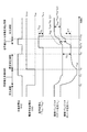
図1は、本発明が適用されるアクティブマトリクス型表示装置の構成の概略を示すシステム構成図である。
<1. Organic EL Display Device to which the Present Invention is Applied>
[1-1. System configuration]
FIG. 1 is a system configuration diagram showing an outline of the configuration of an active matrix display device to which the present invention is applied.
アクティブマトリクス型表示装置は、電気光学素子に流れる電流を、当該電気光学素子と同じ画素内に設けた能動素子、例えば絶縁ゲート型電界効果トランジスタにより制御する表示装置である。絶縁ゲート型電界効果トランジスタとしては、一般には、TFT(薄膜トランジスタ)が用いられる。 An active matrix display device is a display device that controls the current flowing through an electro-optical element by an active element provided in the same pixel as the electro-optical element, for example, an insulated gate field effect transistor. As the insulated gate field effect transistor, a TFT (Thin Film Transistor) is generally used.
ここでは、一例として、デバイスに流れる電流値に応じて発光輝度が変化する電流駆動型の電気光学素子、例えば有機EL素子を画素(画素回路)の発光素子として用いたアクティブマトリクス型有機EL表示装置の場合を例に挙げて説明するものとする。 Here, as an example, an active matrix organic EL display device using, as an example, a current-driven electro-optic element whose emission luminance changes according to the value of current flowing through the device, for example, an organic EL element as a light-emitting element of a pixel (pixel circuit) This case will be described as an example.
図1に示すように、本適用例に係る有機EL表示装置10は、有機EL素子を含む複数の画素20と、当該画素20が行列状に2次元配列されてなる画素アレイ部30と、当該画素アレイ部30の周辺に配置された駆動部とを有する構成となっている。駆動部は、書込み走査回路40、電源供給走査回路50及び信号出力回路60等からなり、画素アレイ部30の各画素20を駆動する。
As shown in FIG. 1, an organic EL display device 10 according to this application example includes a plurality of
ここで、有機EL表示装置10がカラー表示対応の場合は、1つの画素(単位画素)は複数の副画素(サブピクセル)から構成され、この副画素の各々が画素20に相当することになる。より具体的には、カラー表示用の表示装置では、1つの画素は、赤色光(R)を発光する副画素、緑色光(G)を発光する副画素、青色光(B)を発光する副画素の3つの副画素から構成される。
Here, when the organic EL display device 10 supports color display, one pixel (unit pixel) includes a plurality of sub-pixels (sub-pixels), and each of the sub-pixels corresponds to the
但し、1つの画素としては、RGBの3原色の副画素の組み合わせに限られるものではなく、3原色の副画素に更に1色あるいは複数色の副画素を加えて1つの画素を構成することも可能である。より具体的には、例えば、輝度向上のために白色光(W)を発光する副画素を加えて1つの画素を構成したり、色再現範囲を拡大するために補色光を発光する少なくとも1つの副画素を加えて1つの画素を構成したりすることも可能である。 However, one pixel is not limited to a combination of RGB three primary color subpixels, and one pixel may be configured by adding one or more color subpixels to the three primary color subpixels. Is possible. More specifically, for example, at least one sub-pixel that emits white light (W) is added to improve luminance to form one pixel, or at least one that emits complementary color light to expand the color reproduction range. It is also possible to configure one pixel by adding subpixels.
画素アレイ部30には、m行n列の画素20の配列に対して、行方向(画素行の画素の配列方向)に沿って走査線31-1〜31-mと電源供給線32-1〜32-mとが画素行毎に配線されている。更に、列方向(画素列の画素の配列方向)に沿って信号線33-1〜33-nが画素列毎に配線されている。
The pixel array unit 30 includes
走査線31-1〜31-mは、書込み走査回路40の対応する行の出力端にそれぞれ接続されている。電源供給線32-1〜32-mは、電源供給走査回路50の対応する行の出力端にそれぞれ接続されている。信号線33-1〜33-nは、信号出力回路60の対応する列の出力端にそれぞれ接続されている。
The scanning lines 31 -1 to 31 -m are respectively connected to the output ends of the corresponding rows of the writing
画素アレイ部30は、通常、ガラス基板などの透明絶縁基板上に形成されている。これにより、有機EL表示装置10は、平面型(フラット型)のパネル構造となっている。画素アレイ部30の各画素20の駆動回路は、アモルファスシリコンTFTまたは低温ポリシリコンTFTを用いて形成することができる。低温ポリシリコンTFTを用いる場合には、図1に示すように、書込み走査回路40、電源供給走査回路50、及び、信号出力回路60についても、画素アレイ部30を形成する表示パネル(基板)70上に実装することができる。
The pixel array unit 30 is usually formed on a transparent insulating substrate such as a glass substrate. Thereby, the organic EL display device 10 has a flat panel structure. The drive circuit for each
書込み走査回路40は、クロックパルスckに同期してスタートパルスspを順にシフト(転送)するシフトレジスタ等によって構成されている。この書込み走査回路40は、画素アレイ部30の各画素20への映像信号の書込みに際し、走査線31-1〜31-mに対して書込み走査信号WS(WS1〜WSm)を順次供給することによって画素アレイ部30の各画素20を行単位で順番に走査(線順次走査)する。
The
電源供給走査回路50は、クロックパルスckに同期してスタートパルスspを順にシフトするシフトレジスタ等によって構成されている。この電源供給走査回路50は、書込み走査回路40による線順次走査に同期して、第1電源電位Vccpと当該第1電源電位Vccpよりも低い第2電源電位Viniとで切り替わることが可能な電源電位DS(DS1〜DSm)を電源供給線32-1〜32-mに供給する。後述するように、電源電位DSのVccp/Viniの切替えにより、画素20の発光/非発光の制御が行なわれる。
The power
信号出力回路60は、信号供給源(図示せず)から供給される輝度情報に応じた映像信号の信号電圧(以下、単に「信号電圧」と記述する場合もある)Vsigと基準電圧Vofsとを選択的に出力する。ここで、基準電圧Vofsは、映像信号の信号電圧Vsigの基準となる電圧(例えば、映像信号の黒レベルに相当する電圧)であり、後述する閾値補正処理の際に用いられる。
The
信号出力回路60から出力される信号電圧Vsig/基準電圧Vofsは、信号線33-1〜33-nを介して画素アレイ部30の各画素20に対して、書込み走査回路40による走査によって選択された画素行単位で書き込まれる。すなわち、信号出力回路60は、信号電圧Vsigを行(ライン)単位で書き込む線順次書込みの駆動形態を採っている。
The signal voltage V sig / reference voltage V ofs output from the
(画素回路)
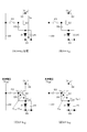
図2は、画素(画素回路)20の具体的な回路構成を示す回路図である。画素20の発光部は、デバイスに流れる電流値に応じて発光輝度が変化する電流駆動型の電気光学素子である有機EL素子21から成る。
(Pixel circuit)
FIG. 2 is a circuit diagram showing a specific circuit configuration of the pixel (pixel circuit) 20. The light-emitting portion of the
図2に示すように、画素20は、有機EL素子21と、当該有機EL素子21に電流を流すことによって有機EL素子21を駆動する駆動回路とによって構成されている。有機EL素子21は、全ての画素20に対して共通に配線(所謂、ベタ配線)された共通電源供給線34にカソード電極が接続されている。
As shown in FIG. 2, the
有機EL素子21を駆動する駆動回路は、駆動トランジスタ22、書込みトランジスタ23、及び、保持容量24を有する構成となっている。駆動トランジスタ22及び書込みトランジスタ23としてNチャネル型のTFTを用いることができる。但し、ここで示した、駆動トランジスタ22及び書込みトランジスタ23の導電型の組み合わせは一例に過ぎず、これらの組み合わせに限られるものではない。
The drive circuit that drives the
尚、駆動トランジスタ22及び書込みトランジスタ23としてNチャネル型のTFTを用いると、アモルファスシリコン(a−Si)プロセスを用いて形成することができる。a−Siプロセスを用いることで、TFTを作成する基板の低コスト化、ひいては本有機EL表示装置10の低コスト化を図ることが可能になる。また、駆動トランジスタ22及び書込みトランジスタ23を同じ導電型の組み合わせにすると、両トランジスタ22,23を同じプロセスで作成することができるために低コスト化に寄与できる。
Note that when an N-channel TFT is used as the driving
駆動トランジスタ22は、一方の電極(ソース/ドレイン電極)が有機EL素子21のアノード電極に接続され、他方の電極(ドレイン/ソース電極)が電源供給線32(32-1〜32-m)に接続されている。
The
書込みトランジスタ23は、一方の電極(ソース/ドレイン電極)が信号線33(33-1〜33-n)に接続され、他方の電極(ドレイン/ソース電極)が駆動トランジスタ22のゲート電極に接続されている。また、書込みトランジスタ23のゲート電極は、走査線31(31-1〜31-m)に接続されている。
The
駆動トランジスタ22及び書込みトランジスタ23において、一方の電極とは、ソース/ドレイン領域に電気的に接続された金属配線を言い、他方の電極とは、ドレイン/ソース領域に電気的に接続された金属配線を言う。また、一方の電極と他方の電極との電位関係によって一方の電極がソース電極ともなればドレイン電極ともなり、他方の電極がドレイン電極ともなればソース電極ともなる。
In the driving
保持容量24は、一方の電極が駆動トランジスタ22のゲート電極に接続され、他方の電極が駆動トランジスタ22の他方の電極、及び、有機EL素子21のアノード電極に接続されている。
The
尚、有機EL素子21の駆動回路としては、駆動トランジスタ22及び書込みトランジスタ23の2つのトランジスタと保持容量24の1つの容量素子とからなる回路構成のものに限られるものではない。例えば、一方の電極が有機EL素子21のアノード電極に、他方の電極が固定電位にそれぞれ接続されることで、有機EL素子21の容量不足分を補う補助容量を必要に応じて設けた回路構成を採ることも可能である。
The drive circuit of the
上記構成の画素20において、書込みトランジスタ23は、書込み走査回路40から走査線31を通してゲート電極に印加されるHighアクティブの書込み走査信号WSに応答して導通状態となる。これにより、書込みトランジスタ23は、信号線33を通して信号出力回路60から供給される、輝度情報に応じた映像信号の信号電圧Vsigまたは基準電圧Vofsをサンプリングして画素20内に書き込む。この書き込まれた信号電圧Vsigまたは基準電圧Vofsは、駆動トランジスタ22のゲート電極に印加されるとともに保持容量24に保持される。
In the
駆動トランジスタ22は、電源供給線32(32-1〜32-m)の電位DSが第1電源電位Vccpにあるときには、一方の電極がドレイン電極、他方の電極がソース電極となって飽和領域で動作する。これにより、駆動トランジスタ22は、電源供給線32から電流の供給を受けて有機EL素子21を電流駆動にて発光駆動する。より具体的には、駆動トランジスタ22は、飽和領域で動作することにより、保持容量24に保持された信号電圧Vsigの電圧値に応じた電流値の駆動電流(直流電流)を有機EL素子21に供給し、当該有機EL素子21を電流駆動することによって発光させる。
When the potential DS of the power supply line 32 (32 -1 to 32 -m ) is at the first power supply potential V ccp , the driving
駆動トランジスタ22は更に、電源電位DSが第1電源電位Vccpから第2電源電位Viniに切り替わったときには、一方の電極がソース電極、他方の電極がドレイン電極となってスイッチングトランジスタとして動作する。これにより、駆動トランジスタ22は、有機EL素子21への駆動電流の供給を停止し、有機EL素子21を非発光状態にする。すなわち、駆動トランジスタ22は、有機EL素子21の発光/非発光を制御するトランジスタとしての機能をも併せ持っている。
Further, when the power supply potential DS is switched from the first power supply potential V ccp to the second power supply potential V ini , the
この駆動トランジスタ22のスイッチング動作により、有機EL素子21が非発光状態となる期間(非発光期間)を設け、有機EL素子21の発光期間と非発光期間の割合(デューティ)を制御することができる。このデューティ制御により、1表示フレーム期間に亘って画素が発光することに伴う残像ボケを低減できるために、特に動画の画品位をより優れたものとすることができる。
By the switching operation of the
電源供給走査回路50から電源供給線32を通して選択的に供給される第1,第2電源電位Vccp,Viniのうち、第1電源電位Vccpは有機EL素子21を発光駆動する駆動電流を駆動トランジスタ22に供給するための電源電位である。また、第2電源電位Viniは、有機EL素子21に対して逆バイアスを掛けるための電源電位である。この第2電源電位Viniは、基準電圧Vofsよりも低い電位、例えば、駆動トランジスタ22の閾値電圧をVthとするときVofs−Vthよりも低い電位、好ましくは、Vofs−Vthよりも十分に低い電位に設定される。
Of the first and second power supply potentials V ccp and V ini selectively supplied from the power
[1−2.基本的な回路動作]
続いて、上記構成の有機EL表示装置10の基本的な回路動作について、図3のタイミング波形図を基に図4及び図5の動作説明図を用いて説明する。尚、図4及び図5の動作説明図では、図面の簡略化のために、書込みトランジスタ23をスイッチのシンボルで図示している。また、有機EL素子21の等価容量25についても図示している。
[1-2. Basic circuit operation]
Next, the basic circuit operation of the organic EL display device 10 having the above-described configuration will be described with reference to the operation explanatory diagrams of FIGS. 4 and 5 based on the timing waveform diagram of FIG. In the operation explanatory diagrams of FIGS. 4 and 5, the
図3のタイミング波形図には、走査線31の電位(書込み走査信号)WS、電源供給線32の電位(電源電位)DS、信号線33の電位(Vsig/Vofs)、駆動トランジスタ22のゲート電位Vg及びソース電位Vsのそれぞれの変化を示している。 In the timing waveform diagram of FIG. 3, the potential of the scanning line 31 (write scanning signal) WS, the potential of the power supply line 32 (power supply potential) DS, the potential of the signal line 33 (V sig / V ofs ), Changes in the gate potential V g and the source potential V s are shown.
(前表示フレームの発光期間)
図3のタイミング波形図において、時刻t11以前は、前の表示フレームにおける有機EL素子21の発光期間となる。この前表示フレームの発光期間では、電源供給線32の電位DSが第1電源電位(以下、「高電位」と記述する)Vccpにあり、また、書込みトランジスタ23が非導通状態にある。
(Light emission period of the previous display frame)
In the timing waveform diagram of FIG. 3, the time before time t 11 is the light emission period of the
このとき、駆動トランジスタ22は飽和領域で動作するように設計されている。これにより、図4(A)に示すように、駆動トランジスタ22のゲート−ソース間電圧Vgsに応じた駆動電流(ドレイン−ソース間電流)Idsが、電源供給線32から駆動トランジスタ22を通して有機EL素子21に供給される。よって、有機EL素子21が駆動電流Idsの電流値に応じた輝度で発光する。
At this time, the
(閾値補正準備期間)
時刻t11になると、線順次走査の新しい表示フレーム(現表示フレーム)に入る。そして、図4(B)に示すように、電源供給線32の電位DSが高電位Vccpから、信号線33の基準電圧Vofsに対してVofs−Vthよりも十分に低い第2電源電位(以下、「低電位」と記述する)Viniに切り替わる。
(Threshold correction preparation period)
At time t 11, it enters a new display frame of line sequential scanning (current display frame). Then, as shown in FIG. 4B, the second power source in which the potential DS of the
ここで、有機EL素子21の閾値電圧をVthel、共通電源供給線34の電位(カソード電位)をVcathとする。このとき、低電位ViniをVini<Vthel+Vcathとすると、駆動トランジスタ22のソース電位Vsが低電位Viniにほぼ等しくなるために、有機EL素子21は逆バイアス状態となって消光する。
Here, the threshold voltage of the
次に、時刻t12で走査線31の電位WSが低電位側から高電位側に遷移することで、図4(C)に示すように、書込みトランジスタ23が導通状態となる。このとき、信号出力回路60から信号線33に対して基準電圧Vofsが供給された状態にあるために、駆動トランジスタ22のゲート電位Vgが基準電圧Vofsになる。また、駆動トランジスタ22のソース電位Vsは、基準電圧Vofsよりも十分に低い電位Viniにある。
Next, at time t 12 , the potential WS of the
このとき、駆動トランジスタ22のゲート−ソース間電圧VgsはVofs−Viniとなる。ここで、Vofs−Viniが駆動トランジスタ22の閾値電圧Vthよりも大きくないと、後述する閾値補正処理を行うことができないために、Vofs−Vini>Vthなる電位関係に設定する必要がある。
At this time, the gate-source voltage V gs of the driving
このように、駆動トランジスタ22のゲート電位Vgを基準電圧Vofsに固定し、ソース電位Vsを低電位Viniに固定して(確定させて)初期化する処理が、後述する閾値補正処理(閾値補動作)を行う前の準備(閾値補正準備)の処理である。従って、基準電圧Vofs及び低電位Viniが、駆動トランジスタ22のゲート電位Vg及びソース電位Vsの各初期化電位となる。
In this way, the process of fixing the gate potential V g of the driving
(閾値補正期間)
次に、時刻t13で、図4(D)に示すように、電源供給線32の電位DSが低電位Viniから高電位Vccpに切り替わると、駆動トランジスタ22のゲート電位Vgが保たれた状態で閾値補正処理が開始される。すなわち、ゲート電位Vgから駆動トランジスタ22の閾値電圧Vthを減じた電位に向けて駆動トランジスタ22のソース電位Vsが上昇を開始する。
(Threshold correction period)
Next, when the potential DS of the
ここでは、便宜上、駆動トランジスタ22のゲート電極の初期化電位Vofsを基準とし、当該初期化電位Vofsから駆動トランジスタ22の閾値電圧Vthを減じた電位に向けてソース電位Vsを変化させる処理を閾値補正処理と呼んでいる。この閾値補正処理が進むと、やがて、駆動トランジスタ22のゲート−ソース間電圧Vgsが駆動トランジスタ22の閾値電圧Vthに収束する。この閾値電圧Vthに相当する電圧は保持容量24に保持される。
Here, for convenience, the initialization potential V ofs of the gate electrode of the
尚、閾値補正処理を行う期間(閾値補正期間)において、電流が専ら保持容量24側に流れ、有機EL素子21側には流れないようにするために、有機EL素子21がカットオフ状態となるように共通電源供給線34の電位Vcathを設定しておくこととする。
In the period for performing the threshold correction process (threshold correction period), the
次に、時刻t14で走査線31の電位WSが低電位側に遷移することで、図5(A)に示すように、書込みトランジスタ23が非導通状態となる。このとき、駆動トランジスタ22のゲート電極が信号線33から電気的に切り離されることによってフローティング状態になる。しかし、ゲート−ソース間電圧Vgsが駆動トランジスタ22の閾値電圧Vthに等しいために、当該駆動トランジスタ22はカットオフ状態にある。従って、駆動トランジスタ22にドレイン−ソース間電流Idsは流れない。
Then, the potential WS of the
(信号書込み&移動度補正期間)
次に、時刻t15で、図5(B)に示すように、信号線33の電位が基準電圧Vofsから映像信号の信号電圧Vsigに切り替わる。続いて、時刻t16で、走査線31の電位WSが高電位側に遷移することで、図5(C)に示すように、書込みトランジスタ23が導通状態になって映像信号の信号電圧Vsigをサンプリングして画素20内に書き込む。
(Signal writing & mobility correction period)
Next, at time t 15 , as shown in FIG. 5B, the potential of the
この書込みトランジスタ23による信号電圧Vsigの書込みにより、駆動トランジスタ22のゲート電位Vgが信号電圧Vsigとなる。そして、映像信号の信号電圧Vsigによる駆動トランジスタ22の駆動の際に、当該駆動トランジスタ22の閾値電圧Vthが保持容量24に保持された閾値電圧Vthに相当する電圧と相殺される。この閾値キャンセルの原理の詳細については後述する。
By writing the signal voltage V sig by the writing
このとき、有機EL素子21はカットオフ状態(ハイインピーダンス状態)にある。従って、映像信号の信号電圧Vsigに応じて電源供給線32から駆動トランジスタ22に流れる電流(ドレイン−ソース間電流Ids)は有機EL素子21の等価容量25に流れ込み、当該等価容量25の充電が開始される。
At this time, the
有機EL素子21の等価容量25が充電されることにより、駆動トランジスタ22のソース電位Vsが時間の経過と共に上昇していく。このとき既に、駆動トランジスタ22の閾値電圧Vthの画素毎のばらつきがキャンセルされており、駆動トランジスタ22のドレイン−ソース間電流Idsは当該駆動トランジスタ22の移動度μに依存したものとなる。駆動トランジスタ22の移動度μは、当該駆動トランジスタ22のチャネルを構成する半導体薄膜の移動度である。
As the
ここで、映像信号の信号電圧Vsigに対する保持容量24の保持電圧Vgsの比率、即ち、書込みゲインGが1(理想値)であると仮定する。すると、駆動トランジスタ22のソース電位VsがVofs−Vth+ΔVの電位まで上昇することで、駆動トランジスタ22のゲート‐ソース間電圧VgsはVsig−Vofs+Vth−ΔVとなる。
Here, it is assumed that the ratio of the holding voltage V gs of the holding
すなわち、駆動トランジスタ22のソース電位Vsの上昇分ΔVは、保持容量24に保持された電圧(Vsig−Vofs+Vth)から差し引かれるように、換言すれば、保持容量24の充電電荷を放電するように作用し、負帰還がかけられたことになる。従って、ソース電位Vsの上昇分ΔVは負帰還の帰還量となる。
That is, the increase ΔV of the source potential Vs of the driving
このように、駆動トランジスタ22に流れるドレイン−ソース間電流Idsに応じた帰還量ΔVでゲート‐ソース間電圧Vgsに負帰還をかけることで、駆動トランジスタ22のドレイン−ソース間電流Idsの移動度μに対する依存性を打ち消すことができる。この打ち消す処理が、駆動トランジスタ22の移動度μの画素毎のばらつきを補正する移動度補正処理である。
Thus, the drain flowing through the driving transistor 22 - gate with the feedback amount ΔV corresponding to the source current I ds - by applying the negative feedback to the source voltage V gs, the drain of the driving transistor 22 - the source current I ds The dependence on mobility μ can be negated. This canceling process is a mobility correction process for correcting the variation of the mobility μ of the driving
より具体的には、駆動トランジスタ22のゲート電極に書き込まれる映像信号の信号振幅Vin(=Vsig−Vofs)が高い程ドレイン−ソース間電流Idsが大きくなるため、負帰還の帰還量ΔVの絶対値も大きくなる。従って、発光輝度レベルに応じた移動度補正処理が行われる。
More specifically, since the drain-source current I ds increases as the signal amplitude V in (= V sig −V ofs ) of the video signal written to the gate electrode of the
また、映像信号の信号振幅Vinを一定とした場合、駆動トランジスタ22の移動度μが大きいほど負帰還の帰還量ΔVの絶対値も大きくなるため、画素毎の移動度μのばらつきを取り除くことができる。従って、負帰還の帰還量ΔVは、移動度補正の補正量とも言える。移動度補正の原理の詳細については後述する。
Furthermore, when a constant signal amplitude V in of the video signal, since the greater the absolute value of the feedback amount ΔV of the mobility μ is large enough negative feedback of the
(発光期間)
次に、時刻t17で走査線31の電位WSが低電位側に遷移することで、図5(D)に示すように、書込みトランジスタ23が非導通状態となる。これにより、駆動トランジスタ22のゲート電極は、信号線33から電気的に切り離されるためにフローティング状態になる。
(Light emission period)
Next, at time t 17 , the potential WS of the
ここで、駆動トランジスタ22のゲート電極がフローティング状態にあるときは、駆動トランジスタ22のゲート−ソース間に保持容量24が接続されていることにより、駆動トランジスタ22のソース電位Vsの変動に連動してゲート電位Vgも変動する。このように、駆動トランジスタ22のゲート電位Vgがソース電位Vsの変動に連動して変動する動作が、保持容量24によるブートストラップ動作である。
Here, when the gate electrode of the
駆動トランジスタ22のゲート電極がフローティング状態になり、それと同時に、駆動トランジスタ22のドレイン−ソース間電流Idsが有機EL素子21に流れ始めることにより、当該電流Idsに応じて有機EL素子21のアノード電位が上昇する。
The gate electrode of the
そして、有機EL素子21のアノード電位がVthel+Vcathを越えると、有機EL素子21に駆動電流が流れ始めるため有機EL素子21が発光を開始する。また、有機EL素子21のアノード電位の上昇は、即ち、駆動トランジスタ22のソース電位Vsの上昇に他ならない。そして、駆動トランジスタ22のソース電位Vsが上昇すると、保持容量24のブートストラップ動作により、駆動トランジスタ22のゲート電位Vgも連動して上昇する。
When the anode potential of the
このとき、ブートストラップゲインが1(理想値)であると仮定した場合、ゲート電位Vgの上昇量はソース電位Vsの上昇量に等しくなる。故に、発光期間中、駆動トランジスタ22のゲート‐ソース間電圧Vgsは、Vsig−Vofs+Vth−ΔVで一定に保持される。そして、時刻t18で信号線33の電位が映像信号の信号電圧Vsigから基準電圧Vofsに切り替わる。
At this time, when it is assumed that the bootstrap gain is 1 (ideal value), the increase amount of the gate potential V g becomes equal to the increase amount of the source potential V s . Therefore, during the light emission period, the gate-source voltage V gs of the
以上説明した一連の回路動作において、閾値補正準備、閾値補正、信号電圧Vsigの書込み(信号書込み)、及び、移動度補正の各処理動作は、1水平走査期間(1H)において実行される。また、信号書込み及び移動度補正の各処理動作は、時刻t6−t7の期間において並行して実行される。 In the series of circuit operations described above, processing operations for threshold correction preparation, threshold correction, signal voltage V sig writing (signal writing), and mobility correction are executed in one horizontal scanning period (1H). Further, the signal writing and mobility correction processing operations are executed in parallel during the period of time t 6 -t 7 .
〔分割閾値補正〕
尚、ここでは、閾値補正処理を1回だけ実行する駆動法を採る場合を例に挙げて説明したが、この駆動法は一例に過ぎず、この駆動法に限られるものではない。例えば、閾値補正処理を移動度補正及び信号書込み処理と共に行う1H期間に加えて、当該1H期間に先行する複数の水平走査期間に亘って分割して複数回閾値補正処理を実行する、所謂分割閾値補正を行う駆動法を採ることも可能である。
[Division threshold correction]
Here, the case where the driving method in which the threshold value correction process is executed only once is described as an example, but this driving method is only an example and is not limited to this driving method. For example, in addition to the 1H period in which the threshold correction process is performed together with the mobility correction and the signal writing process, the so-called divided threshold is executed by dividing the threshold correction process over a plurality of horizontal scanning periods preceding the 1H period and performing the threshold correction process a plurality of times. It is also possible to adopt a driving method for performing correction.
この分割閾値補正の駆動法によれば、高精細化に伴う多画素化によって1水平走査期間に割り当てられる時間が短くなったとしても、閾値補正期間として複数の水平走査期間に亘って十分な時間を確保することができるために、閾値補正処理を確実に行うことができる。 According to this division threshold correction driving method, even if the time allotted to one horizontal scanning period is shortened due to the increase in the number of pixels accompanying high definition, sufficient time is provided for a plurality of horizontal scanning periods as the threshold correction period. Therefore, the threshold value correction process can be performed reliably.
〔閾値キャンセルの原理〕
ここで、駆動トランジスタ22の閾値キャンセル(即ち、閾値補正)の原理について説明する。駆動トランジスタ22は、飽和領域で動作するように設計されているために定電流源として動作する。これにより、有機EL素子21には駆動トランジスタ22から、次式(1)で与えられる一定のドレイン−ソース間電流(駆動電流)Idsが供給される。
Ids=(1/2)・μ(W/L)Cox(Vgs−Vth)2 ……(1)
ここで、Wは駆動トランジスタ22のチャネル幅、Lはチャネル長、Coxは単位面積当たりのゲート容量である。
[Principle of threshold cancellation]
Here, the principle of threshold cancellation (that is, threshold correction) of the
I ds = (1/2) · μ (W / L) C ox (V gs −V th ) 2 (1)
Here, W is the channel width of the driving
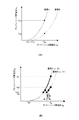
図6(A)に、駆動トランジスタ22のドレイン−ソース間電流Ids対ゲート−ソース間電圧Vgsの特性を示す。
FIG. 6A shows the characteristics of the drain-source current I ds versus the gate-source voltage V gs of the driving
この特性図に示すように、駆動トランジスタ22の閾値電圧Vthの画素毎のばらつきに対するキャンセル処理を行わないと、閾値電圧VthがVth1のとき、ゲート−ソース間電圧Vgsに対応するドレイン−ソース間電流IdsがIds1になる。
As shown in this characteristic diagram, when the cancellation process for the variation of the threshold voltage V th of the driving
これに対して、閾値電圧VthがVth2(Vth2>Vth1)のとき、同じゲート−ソース間電圧Vgsに対応するドレイン−ソース間電流IdsがIds2(Ids2<Ids1)になる。すなわち、駆動トランジスタ22の閾値電圧Vthが変動すると、ゲート−ソース間電圧Vgsが一定であってもドレイン−ソース間電流Idsが変動する。
On the other hand, when the threshold voltage V th is V th2 (V th2> V th1 ), the same gate - drain corresponding to the source voltage V gs - source current I ds I ds2 (I ds2 <I ds1 ) become. That is, when the threshold voltage V th of the
一方、上記構成の画素(画素回路)20では、先述したように、発光時の駆動トランジスタ22のゲート−ソース間電圧VgsはVsig−Vofs+Vth−ΔVである。従って、これを式(1)に代入すると、ドレイン−ソース間電流Idsは、次式(2)で表される。
Ids=(1/2)・μ(W/L)Cox(Vsig−Vofs−ΔV)2 ……(2)
On the other hand, in the pixel (pixel circuit) 20 having the above configuration, as described above, the gate-source voltage V gs of the driving
I ds = (1/2) · μ (W / L) C ox (V sig −V ofs −ΔV) 2 (2)
すなわち、駆動トランジスタ22の閾値電圧Vthの項がキャンセルされており、駆動トランジスタ22から有機EL素子21に供給されるドレイン−ソース間電流Idsは、駆動トランジスタ22の閾値電圧Vthに依存しない。その結果、駆動トランジスタ22の製造プロセスのばらつきや経時変化等により、駆動トランジスタ22の閾値電圧Vthが画素毎に変動したとしても、ドレイン−ソース間電流Idsが変動しないために、有機EL素子21の発光輝度を一定に保つことができる。
That is, the term of the threshold voltage V th of the
〔移動度補正の原理〕
次に、駆動トランジスタ22の移動度補正の原理について説明する。図6(B)に、駆動トランジスタ22の移動度μが相対的に大きい画素Aと、駆動トランジスタ22の移動度μが相対的に小さい画素Bとを比較した状態で特性カーブを示す。駆動トランジスタ22をポリシリコン薄膜トランジスタなどで構成した場合、画素Aや画素Bのように、画素間で移動度μがばらつくことは避けられない。
[Principle of mobility correction]
Next, the principle of mobility correction of the
画素Aと画素Bで移動度μにばらつきがある状態で、駆動トランジスタ22のゲート電極に例えば両画素A,Bに同レベルの信号振幅Vin(=Vsig−Vofs)を書き込んだ場合を考える。この場合、何ら移動度μの補正を行わないと、移動度μの大きい画素Aに流れるドレイン−ソース間電流Ids1′と移動度μの小さい画素Bに流れるドレイン−ソース間電流Ids2′との間には大きな差が生じてしまう。このように、移動度μの画素毎のばらつきに起因してドレイン−ソース間電流Idsに画素間で大きな差が生じると、画面のユニフォーミティ(一様性)が損なわれる。
A case where the signal amplitude V in (= V sig −V ofs ) of the same level is written to both the pixels A and B, for example, in the gate electrode of the driving
ここで、先述した式(1)のトランジスタ特性式から明らかなように、移動度μが大きいとドレイン−ソース間電流Idsが大きくなる。従って、負帰還における帰還量ΔVは移動度μが大きくなるほど大きくなる。図6(B)に示すように、移動度μの大きな画素Aの帰還量ΔV1は、移動度の小さな画素Bの帰還量ΔV2に比べて大きい。 Here, as is clear from the transistor characteristic equation of the equation (1) described above, the drain-source current I ds increases when the mobility μ is large. Therefore, the feedback amount ΔV in the negative feedback increases as the mobility μ increases. As shown in FIG. 6B, the feedback amount ΔV 1 of the pixel A having the high mobility μ is larger than the feedback amount ΔV 2 of the pixel B having the low mobility μ.
そこで、移動度補正処理によって駆動トランジスタ22のドレイン−ソース間電流Idsに応じた帰還量ΔVでゲート−ソース間電圧Vgsに負帰還をかけることにより、移動度μが大きいほど負帰還が大きくかかることになる。その結果、移動度μの画素毎のばらつきを抑制することができる。
Therefore, by applying negative feedback to the gate-source voltage Vgs with a feedback amount ΔV corresponding to the drain-source current I ds of the driving
具体的には、移動度μの大きな画素Aで帰還量ΔV1の補正をかけると、ドレイン−ソース間電流IdsはIds1′からIds1まで大きく下降する。一方、移動度μの小さな画素Bの帰還量ΔV2は小さいために、ドレイン−ソース間電流IdsはIds2′からIds2までの下降となり、それ程大きく下降しない。結果的に、画素Aのドレイン−ソース間電流Ids1と画素Bのドレイン−ソース間電流Ids2とはほぼ等しくなるために、移動度μの画素毎のばらつきが補正される。 Specifically, when applying a correction of the feedback amount [Delta] V 1 at the pixel A having the high mobility mu, drain - source current I ds larger drops from I ds1 'to I ds1. On the other hand, since the feedback amount [Delta] V 2 small pixels B mobility μ is small, the drain - source current I ds becomes lowered from I ds2 'to I ds2, not lowered so much. Consequently, the drain of the pixel A - drain-source current I ds1 and the pixel B - to become nearly equal to the source current I ds2, variations among the pixels of the mobility μ is corrected.
以上をまとめると、移動度μの異なる画素Aと画素Bがあった場合、移動度μの大きい画素Aの帰還量ΔV1は移動度μの小さい画素Bの帰還量ΔV2に比べて大きくなる。つまり、移動度μが大きい画素ほど帰還量ΔVが大きく、ドレイン−ソース間電流Idsの減少量が大きくなる。 In summary, when there are a pixel A and a pixel B having different mobility μ, the feedback amount ΔV1 of the pixel A having a high mobility μ is larger than the feedback amount ΔV2 of the pixel B having a low mobility μ. That is, the larger the mobility μ, the larger the feedback amount ΔV, and the larger the amount of decrease in the drain-source current I ds .
従って、駆動トランジスタ22のドレイン−ソース間電流Idsに応じた帰還量ΔVで、ゲート−ソース間電圧Vgsに負帰還をかけることで、移動度μの異なる画素のドレイン−ソース間電流Idsの電流値が均一化される。その結果、移動度μの画素毎のばらつきを補正することができる。すなわち、駆動トランジスタ22に流れる電流(ドレイン−ソース間電流Ids)に応じた帰還量ΔVで、駆動トランジスタ22のゲート−ソース間電圧Vgsに負帰還をかける処理が移動度補正処理となる。
Therefore, the drain of the driving transistor 22 - with the feedback amount ΔV corresponding to the source current I ds, the gate - by applying the negative feedback to the source voltage V gs, the drain of pixels having different mobilities mu - source current I ds The current value is made uniform. As a result, variation in mobility μ for each pixel can be corrected. That is, the process of applying negative feedback to the gate-source voltage V gs of the
[1−3.ミラー型レイアウト構造について]
以上説明した有機EL表示装置10において、画素アレイ部30の効率的なレイアウトを図ったり、レイアウトの自由度を上げたりするには、画素(画素回路)20に関して、基本的に同じレイアウト形状とした上で、ミラー型レイアウト構造を採るのが好ましい。前にも述べたように、ミラー型レイアウト構造は、画素アレイ部30の行列状の画素配列の列方向の軸を挟んで隣接する奇数列の画素回路と偶数列の画素回路とを、当該列方向の軸に関して対称にレイアウトする構造である。
[1-3. Mirror type layout structure]
In the organic EL display device 10 described above, in order to achieve an efficient layout of the pixel array unit 30 and increase the degree of freedom of layout, the pixel (pixel circuit) 20 has basically the same layout shape. In the above, it is preferable to adopt a mirror type layout structure. As described above, the mirror-type layout structure includes the pixel circuits in the odd-numbered columns and the pixel circuits in the even-numbered columns that are adjacent to each other across the column-direction axis of the matrix-like pixel array of the pixel array unit 30. The structure is laid out symmetrically with respect to the direction axis.
ここで言う、「列方向の軸に関して対称」の「対称」の概念には、奇数列の画素回路と偶数列の画素回路とが物理的に厳密に対称である場合の他、回路構成素子の設計上あるいは製造上生ずる種々のばらつきや、色の違いに伴う素子サイズの違い等の存在も含まれるものとする。ここで、ミラー型レイアウト構造について具体的に説明する。 Here, the concept of “symmetry” of “symmetric about the axis in the column direction” includes the case where the pixel circuit of the odd-numbered column and the pixel circuit of the even-numbered column are physically strictly symmetrical, The existence of various variations in design or manufacturing, differences in element sizes due to differences in colors, and the like are also included. Here, the mirror type layout structure will be specifically described.
図7は、ミラー型レイアウト構造の一例を示す回路図であり、図中、図2と同等部位には同一符号を付して示している。ここでは、図面の簡略化のために、i行、i+1行の2行、及び、j−1列、j列、j+1列の3列の計6画素についての行列状の画素配列を示している。また、便宜上、例えば、j−1列、j+1列を奇数列とし、j列を偶数列とする。 FIG. 7 is a circuit diagram showing an example of a mirror type layout structure. In FIG. 7, the same parts as those in FIG. 2 are denoted by the same reference numerals. Here, for simplification of the drawing, i row, two rows of row i + 1, and, j-1 row, j column shows the matrix-shaped pixel array for a total of six pixels of three columns j + 1 column . For convenience, for example, j-1 column and j + 1 column are odd columns, and j column is an even column.
図7では、上記の画素配列において、当該画素配列の列方向の軸Yを挟んで隣接する偶数列jに属する画素回路20i,j及び画素回路20i+1,jと、奇数列j+1に属する画素回路20i,j+1及び画素回路20i+1,j+1とをミラー型レイアウト構造としている。具体的には、図7から明らかなように、偶数列jの信号線33-j及び奇数列j+1の信号線33-j+1が共に列方向の軸Y側に配線されている。そして、有機EL素子21、駆動トランジスタ22、書込みトランジスタ23、及び、保持容量24の各回路構成素子が、列方向の軸Yに関して左右対称に配置されている。
In FIG. 7, in the above pixel array, the
このミラー型レイアウト構造によれば、画素アレイ部30の効率的なレイアウトを図ることができる。具体的には、隣接する2列の画素回路間に、列方向に沿って電源線を配線して当該電源線を2列の画素回路間で共有したり、2列の画素回路間でコンタクトホールを共有したり、配線の引き込みラインを途中まで共用したりすることができる。また、ミラー型レイアウト構造によれば、レイアウトの自由度が上がるとともに、レイアウトの密度を下げることができるために、高歩留り化を図ることができる。 According to this mirror type layout structure, an efficient layout of the pixel array unit 30 can be achieved. Specifically, a power supply line is wired between two adjacent pixel circuits in the column direction so that the power supply line is shared between the two pixel circuits, or a contact hole is provided between the two pixel circuits. Can be shared, or the wiring lead-in line can be shared halfway. Further, according to the mirror type layout structure, the degree of freedom in layout is increased and the density of the layout can be lowered, so that a high yield can be achieved.
ここで、共有する電源線としては、例えば、次の例を挙げることができる。図2に示す画素回路20では、信号線33から書込みトランジスタ23を通して閾値補正のための基準電圧Vofsを、駆動トランジスタ22のゲート電極に書き込む構成を採っている。これに対して、基準電圧Vofsを伝送する専用の電源線を、例えばj−1列の画素列とj列の画素列との間に列方向に沿って配線し、当該電源線をj−1列に属する画素回路20i,j-1及び画素回路20i+1,j-1と、j列に属する画素回路20i,j及び画素回路20i+1,jとで共有する構成などが考えられる(その詳細については後述する)。
Here, examples of the shared power line include the following example. The
上述したように、2列の画素回路間で電源線を共有したり、コンタクトホールを共有したり、配線の引き込みラインを途中まで共用したりすることで、画素アレイ部30の効率的なレイアウトを図ることができる。 As described above, an efficient layout of the pixel array unit 30 can be achieved by sharing a power supply line, a contact hole, or a wiring lead-in line halfway between two columns of pixel circuits. Can be planned.
[1−4.セレクタ駆動方式について]
図1において、表示パネル70上の信号出力回路60には、表示パネル70の外部に設けられる駆動部、例えばドライバICから映像信号の信号電圧Vsigと閾値補正のための基準電圧Vofsとが選択的に供給される。ここでは、理解を容易にするために、映像信号の信号電圧Vsigが表示信号として供給される場合の信号出力回路60について説明する。
[1-4. About selector drive system]
In FIG. 1, the
信号出力回路60は、ドライバICの出力数の削減を図るために、周知のセレクタ駆動方式を採用している。前にも述べたように、セレクタ駆動方式は、ドライバICの1つの出力に対して、表示パネル70上の信号線33-1〜33-nを複数の信号線を単位(組)として割り当て、ドライバICから時系列で出力される信号電圧Vsigを、複数の信号線に対して時間分割的(時分割)に分配する駆動方式である。
The
一般的には、ドライバICの出力数と表示パネル70上の信号線33-1〜33-nの本数とは等しく設定され、ドライバICの出力端と表示パネル70上の信号線33-1〜33-nとは1対1の対応関係をもって入力信号線によって接続される。しかし、この構成を採ると、ドライバICの出力数がn個、当該ドライバICの出力端と表示パネル70とを電気的に接続する配線(入力信号線)がn本必要となるとともに、表示パネル70側の端子数もn個必要となるため、システム全体の構成が煩雑になる。
In general, it sets equal to the
これに対して、セレクタ駆動方式を採用し、ドライバICの出力と表示パネル70上の信号線33-1〜33-nとの関係を1対x(xは2以上の整数)の対応関係をもって設定する。そして、ドライバICの1つの出力端に対して割り当てられたx本の信号線に対し、当該1つの出力端から時系列で出力される信号電圧Vsigを時間分割的に分配する。このセレクタ駆動方式を採用することで、ドライバICの出力数、当該ドライバICと表示パネル70との間の配線数、及び、表示パネル70側の端子数を信号線33-1〜33-nの本数nの1/xに削減可能になる。
On the other hand, the selector driving method is adopted, and the relationship between the output of the driver IC and the
セレクタ駆動方式を採用する際の単位となる信号線の本数x、即ち、時分割数xとしては、例えば、RGBの3つの副画素によって1つの単位画素を形成する、カラー表示対応の有機EL表示装置の場合には、x=3、またはその倍数に設定するのが好ましい。そして、RGBRGB・・・と3つの副画素が繰り返し配列される1つの画素行に対する、セレクタ回路による信号のセレクト方式は、2つのセレクト方式に大別される。 The number x of signal lines as a unit when adopting the selector driving method, that is, the time division number x is, for example, an organic EL display corresponding to color display in which one unit pixel is formed by three sub-pixels of RGB. In the case of an apparatus, it is preferable to set x = 3 or a multiple thereof. The signal selection method by the selector circuit for one pixel row in which RGBRGB... And three sub-pixels are repeatedly arranged is roughly divided into two selection methods.
2つのセレクト方式のうち、第1のセレクト方式は、例えば、1画素がRGBの副画素から成るとき、3画素を組として1つの色の副画素に対して時間分割的に信号を書き込む方式である。第2のセレクト方式は、1画素のRGBの副画素に対して時間分割的に信号を書き込む方式である。尚、RGBの3つの副画素の色の配列順や信号の書込み順は任意である。ここでは、1画素がRGBの副画素から成る場合を例に挙げたが、基本的には、単色の場合も同様である。 Of the two select methods, the first select method is a method in which, for example, when one pixel is made up of RGB sub-pixels, a signal is written in a time division manner to one color sub-pixel with three pixels as a set. is there. The second selection method is a method of writing a signal in a time division manner to one RGB sub-pixel. Note that the order of color arrangement and signal writing order of the three sub-pixels of RGB are arbitrary. Here, the case where one pixel is made up of RGB sub-pixels is taken as an example, but basically the same applies to the case of a single color.
図8は、セレクタ駆動方式を採る信号出力回路60の構成の一例を示す回路図である。ここでは、図面の簡略化のために、5行12列の画素配列として示している。また、RGBの3つの副画素に対応して時分割数xがx=3の場合で、信号のセレクト方式としては、3画素を組として1つの色の副画素に対して時間分割的に信号を書き込む第1のセレクト方式を採る場合を例に挙げて示している。
FIG. 8 is a circuit diagram showing an example of the configuration of the
図8に示すように、RGBの各画素列に対応してセレクタ回路61,62,63,・・・が配置されている。セレクタ回路61,62,63,・・・は、RGBの各画素列に対応した3つのスイッチSWR,SWG,SWBによって構成され、3つのセレクタ回路を単位として繰り返して配列されている。
As shown in FIG. 8,
そして、3つのセレクタ回路61,62,63の各3つのスイッチSWR,SWG,SWBに対して、3つの端子71R,71G,71Bを介して時系列の信号SIG(1R,2R,3R) ,SIG(1G,2G,3G) ,SIG(1B,2B,3B)が入力される。同様に、次の組の3つのセレクタ回路64(65,66)の各3つのスイッチSWR,SWG,SWBに対して、次の3つの端子72R,72G,72Bを介して時系列の信号SIG(4R,5R,6R) ,SIG(4G,5G,6G) ,SIG(4B,5B,6B)が入力される。
Then, a time series signal SIG (1R, 1) is supplied to each of the three switches SW R , SW G , SW B of the three
また、セレクタ回路61,62,63,・・・には、3つのセレクタ回路を単位として3つの選択信号SEL1,SEL2,SEL3が端子73-1,73-2,73-3を介して与えられる。これらの選択信号SEL1,SEL2,SEL3は、3つを組とするセレクタ回路61,62,63,・・・の3つのスイッチSWR,SWG,SWBをON/OFF制御する。
Further, in the
図9は、セレクタ駆動方式の動作タイミングを示すタイミングチャートである。図9には、垂直走査信号Vscan、3つの選択信号SEL1,SEL2,SEL3、及び、時系列の信号SIG(1R,2R,3R) ,SIG(1G,2G,3G) ,SIG(1B,2B,3B) ,・・・のタイミング関係を示している。このタイミングチャートから明らかなように、時系列の信号SIG(1R,2R,3R) ,SIG(1G,2G,3G) ,SIG(1B,2B,3B) ,・・・が、セレクタ回路61,62,63,・・・によって時間分割的に3本を単位とする信号線33に対して書き込まれる。
FIG. 9 is a timing chart showing the operation timing of the selector driving method. FIG. 9 shows a vertical scanning signal V scan , three selection signals SEL 1 , SEL 2 , SEL 3 , and time series signals SIG (1R, 2R, 3R) , SIG (1G, 2G, 3G) , SIG ( 1B, 2B, 3B) ,... As is apparent from this timing chart, the time series signals SIG (1R, 2R, 3R) , SIG (1G, 2G, 3G) , SIG (1B, 2B, 3B) ,. , 63,... Are written to the
[1−5.2つの信号線が隣接する場合の不具合について]
先述したように、例えば、ミラー型レイアウト構造を採ると、隣接する画素列に属する画素回路に接続される2つの信号線が隣接して配線されるレイアウト構造となる場合がある。このように、2つの信号線が隣接して配線されるレイアウト構造に対して、セレクタ駆動方式を適用する際に、隣接する2つの信号線に対する表示信号の書込みのタイミングが異なると、不具合が生じる場合がある。具体的には、先に信号線に書き込まれた表示信号が、後に信号線に書き込まれる表示信号の影響を受けるため、正確な表示信号を書き込むことができないことになる。この不具合について、以下に具体的に説明する。
[1-5. Problems when two signal lines are adjacent]
As described above, for example, when a mirror layout structure is adopted, there may be a layout structure in which two signal lines connected to pixel circuits belonging to adjacent pixel columns are adjacently wired. As described above, when the selector driving method is applied to a layout structure in which two signal lines are arranged adjacent to each other, a problem occurs if display signal writing timings for the two adjacent signal lines are different. There is a case. Specifically, since the display signal written to the signal line first is affected by the display signal written to the signal line later, an accurate display signal cannot be written. This problem will be specifically described below.
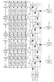
図10は、2つの信号線が隣接して配線されるレイアウト構造の一例を示す回路図であり、図中、図8と同等部位には同一符号を付して示している。 FIG. 10 is a circuit diagram showing an example of a layout structure in which two signal lines are arranged adjacent to each other. In FIG. 10, parts equivalent to those in FIG.
図10に示す5行12列の画素配列において、2列目、3列目の画素列間で信号線33-2と信号線33-3が隣接し、4列目、5列目の画素列間で信号線33-4と信号線33-5が隣接している。同様に、6列目、7列目の画素列間で信号線33-6と信号線33-7が隣接し、8列目、9列目の画素列間で信号線33-8と信号線33-9が隣接し、10列目、11列目の画素列間で信号線33-10と信号線33-11が隣接している。
In the pixel array of 5 rows and 12 columns shown in FIG. 10, the
このように、2つの信号線が隣接すると、図11に示すように、隣接する2つの信号線33-2,33-3間、信号線33-4,33-5間、信号線33-6,33-7間、信号線33-8,33-9間、及び、信号線33-10,33-11間に寄生容量Cpが形成される。そして、寄生容量Cpが形成された状態において、先述したセレクタ駆動方式の場合と同様の動作タイミングでセレクタ回路61,62,63,・・・の駆動が行われるものとする。
Thus, when two signal lines are adjacent, as shown in FIG. 11, between two
このときの動作タイミングを図12に示す。図12の動作タイミングは、基本的に、図9の動作タイミングと同等である。そのため、配線間に寄生容量Cpが形成された状態にある2つの信号線に対する、セレクタ回路61,62,63,・・・の選択タイミングが同じであれば、正確な表示信号を書き込むことが可能である。例えば、2つの信号線33-2,33-3に対するセレクタ回路61の選択タイミングが同じであるため、正確な表示信号SIG1G,SIG1Bを書き込むことができる。
The operation timing at this time is shown in FIG. The operation timing in FIG. 12 is basically the same as the operation timing in FIG. Therefore, if the selection timings of the
一方、配線間に寄生容量Cpが形成された状態にある2つの信号線に対する、セレクタ回路61,62,63,・・・の選択タイミングが異なれば、正確な表示信号を書き込むことができない。例えば、2つの信号線33-6,33-7に対するセレクタ回路62,63の選択タイミングが異なるため、図12のタイミングチャートから明らかなように、正確な表示信号SIG2B,SIG3Rを書き込むことができない。
On the other hand, if the selection timings of the
具体的には、信号線33-6に表示信号SIG2Bを書き込み、当該表示信号SIG2Bを信号線33-6に保持した後、信号線33-7に表示信号SIG3Rを書き込むときに、寄生容量Cpによるカップリングのために、先に書き込んだ表示信号SIG2Bが変動してしまう。表示信号SIG3Rの書込み時の表示信号SIG2Bの電圧変動量をΔSIG2Bとすると、当該電圧変動量ΔSIG2Bは、次式(3)で与えられる。
ΔSIG2B=C6-7/C6・ΔSIG3R ……(3)
ここで、C6-7は2つの信号線33-6,33-7の寄生容量Cpの容量値、C6は信号線33-6の容量値、ΔSIG3Rは表示信号SIG3Rの書込み時の当該表示信号SIG3Rの電圧変動量である。
Specifically, write a display signal SIG 2B to the
ΔSIG 2B = C 6-7 / C 6 · ΔSIG 3R (3)
Here, C 6-7 is the capacitance value of the parasitic capacitance C p of the two
図12のタイミングチャートに示すように、表示信号SIG2B,SIG4B,SIG7Rに関して、本来破線で示す信号波形であるべきところが、寄生容量Cpによるカップリングの影響を受けて、実線で示す信号波形のように電圧の変動が発生する。図12のタイミングチャートにおいて、○印で示したポイントが、垂直走査信号Vscanがアクティブ状態から非アクティブ状態に遷移する瞬間、即ち、書き込んだ表示信号のホールドポイントである。従って、寄生容量Cpのカップリングによる電圧変動が生じた状態のまま、書き込んだ表示信号がホールドされることになる。 As shown in the timing chart of FIG. 12, the display signals SIG 2B , SIG 4B , and SIG 7R are signals that are supposed to be signal waveforms that are originally shown by broken lines but that are shown by solid lines because of the influence of coupling due to parasitic capacitance C p. Voltage fluctuation occurs like a waveform. In the timing chart of FIG. 12, a point indicated by a circle is a moment when the vertical scanning signal V scan transits from an active state to an inactive state, that is, a hold point of the written display signal. Therefore, the written display signal is held in a state in which the voltage variation due to the coupling of the parasitic capacitance C p occurs.
このように、隣接する2つの信号線間に寄生容量Cpが存在していると、当該2つの信号線に対するセレクタ回路61,62,63,・・・の選択タイミングが異なると不具合が生じる。具体的には、上述したように、先に信号線に書き込まれた表示信号が、後に信号線に書き込まれる表示信号の影響を受けるため、正確な表示信号を書き込むことができない。そして、正確な表示信号を信号線に書き込めないと、表示画像の画質の劣化を招くことになる。
As described above, if the parasitic capacitance C p exists between two adjacent signal lines, a problem occurs if the selection timings of the
かかる不具合を解消するための、即ち、隣接する2つの画素列に属する各信号線に対する表示信号の書込みのタイミングが異なっても、正確な表示信号の書込みを可能にするための具体的な実施形態について、以下に、第1実施形態として説明する。 A specific embodiment for eliminating such inconvenience, that is, for enabling accurate writing of a display signal even when the timing of writing a display signal to each signal line belonging to two adjacent pixel columns is different. Is described below as a first embodiment.
<2.第1実施形態>
上述したミラー型レイアウト構造やセレクタ駆動方式については、有機EL表示装置や液晶表示装置等の平面型表示装置において適宜採用することができる。但し、以下に説明する本発明の各実施形態に係る有機EL表示装置においては、セレクタ駆動方式の採用は必須であるが、ミラー型レイアウト構造の採用に関しては任意である。
<2. First Embodiment>
The above-described mirror type layout structure and selector driving method can be appropriately employed in flat display devices such as organic EL display devices and liquid crystal display devices. However, in the organic EL display device according to each embodiment of the present invention described below, the adoption of the selector driving method is indispensable, but the adoption of the mirror type layout structure is arbitrary.
そして、本発明の第1実施形態では、セレクタ駆動方式を採用する有機EL表示装置において、信号線33-1〜33-nをレイアウトするに当たって、隣接する2つの画素列に属する画素回路にそれぞれ接続される2つの信号線のレイアウト方法(レイアウト構造)を特徴とする。
In the first embodiment of the present invention, when the
具体的には、隣接する2つの画素列に属する画素回路にそれぞれ接続される2つの信号線の組み合わせにおいて、セレクタ回路によって異なるタイミングで表示信号が分配される組み合わせについては2つの信号線を隣接しないように配線する(第1の配線領域)。また、セレクタ回路によって同一のタイミングで表示信号が分配される組み合わせについては2つの信号線を隣接して配線する(第2の配線領域)。そして、画素アレイ部30がこれら第1,第2の配線領域を少なくとも一部に有する。 Specifically, in the combination of two signal lines respectively connected to the pixel circuits belonging to two adjacent pixel columns, the two signal lines are not adjacent for the combination in which the display signal is distributed at different timings by the selector circuit. (1st wiring area | region). For the combination in which the display signal is distributed at the same timing by the selector circuit, two signal lines are wired adjacent to each other (second wiring region). The pixel array unit 30 has at least a part of these first and second wiring regions.
セレクタ回路61,62,63,・・・によって異なるタイミングで表示信号が分配される組み合わせについては、2つの信号線が隣接していないことで、当該2つの信号線間には寄生容量Cpが存在しない。従って、2つの信号線に対して異なるタイミングで表示信号が書き込まれても、先に信号線に書き込まれた表示信号が、寄生容量Cpによるカップリングより、後に信号線に書き込まれる表示信号の影響を受けることはない。
For combinations in which display signals are distributed at different timings depending on the
また、セレクタ回路61,62,63,・・・によって同一のタイミングで表示信号が分配される組み合わせについては、2つの信号線が隣接していることで、当該2つの信号線間には寄生容量Cpが存在することになる。しかし、寄生容量Cpが存在していても、2つの信号線に対して表示信号が同一のタイミングで書き込まれるため、共に相手方の表示信号の影響を受けることはない。従って、2つの信号線の組み合わせのいずれの場合においても、信号線に対する正確な表示信号の書込みが可能になる。
Further, for combinations in which display signals are distributed at the same timing by the
上述したように、隣接する2つの画素列に属する各信号線に対する、表示信号の書込みのタイミングが異なっても、正確な表示信号を信号線に書き込むことができる。従って、隣接する信号線間にシールド線を配線する構造を採らなくても、従来技術のような、寄生容量Cpのカップリングの影響による画質劣化を抑えることができるため、高画質の表示画像を得ることができる。 As described above, an accurate display signal can be written to a signal line even when the display signal writing timing differs for each signal line belonging to two adjacent pixel columns. Therefore, since it is possible to suppress image quality degradation due to the influence of the coupling of the parasitic capacitance C p as in the prior art without adopting a structure in which a shield line is provided between adjacent signal lines, a high-quality display image can be obtained. Can be obtained.
尚、隣接する2つの画素列に属する画素回路にそれぞれ接続される2つの信号線が、画素列間において隣接するレイアウト構造としては、例えば、先述したミラー型レイアウト構造が挙げられるが、本実施形態は、ミラー型レイアウト構造への適用に限られるものではない。すなわち、本実施形態は、画素列間において2つの信号線が隣接するレイアウト構造全般に対して適用可能である。以下に、第1実施形態の具体的な実施例について説明する。 As a layout structure in which two signal lines respectively connected to pixel circuits belonging to two adjacent pixel columns are adjacent to each other between the pixel columns, for example, the above-described mirror layout structure can be cited. Is not limited to application to a mirror type layout structure. In other words, this embodiment can be applied to all layout structures in which two signal lines are adjacent between pixel columns. Specific examples of the first embodiment will be described below.
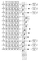
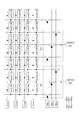
[2−1.実施例1]
図13は、実施例1に係る画素アレイ部のレイアウト構造を示す回路図であり、図中、図10と同等部位には同一符号を付して示している。ここでは、図面の簡略化のために、5行12列の画素配列として示している。また、RGBの3つの副画素に対応して時分割数xをx=3としている。
[2-1. Example 1]
FIG. 13 is a circuit diagram showing the layout structure of the pixel array section according to the first embodiment. In the figure, the same parts as those in FIG. 10 are denoted by the same reference numerals. Here, for simplification of the drawing, a pixel array of 5 rows and 12 columns is shown. Further, the time division number x is set to x = 3 corresponding to the three RGB sub-pixels.
また、セレクタ回路61,62,63,・・・による信号のセレクト方式としては、3画素を組として1つの色の副画素に対して時間分割的に信号を書き込む第1のセレクト方式を採る場合を例に挙げて示している。第1のセレクト方式では、最初の組のセレクタ回路61,62,63には、外部のドライバICから端子71R,71G,71Bを介して各色の時系列の信号が表示信号として入力される。
In addition, as a signal selection method using the
具体的には、端子71Rを介してRの時系列の信号SIG1R,SIG2R,SIG3Rが、端子71Gを介してGの時系列の信号SIG1G,SIG2G,SIG3Gが、端子71Bを介してBの時系列の信号SIG1B,SIG2B,SIG3Bがセレクタ回路61,62,63に入力される。次の組以降のセレクタ回路64,・・・についても、最初の組のセレクタ回路61,62,63と同様に時系列の信号が入力される。
Specifically, the R time-series signals SIG 1R , SIG 2R , SIG 3R are connected via the
これにより、第1のセレクト方式を採るセレクタ駆動方式では、1つの画素を構成するRGBの副画素には、選択信号SEL1,SEL2,SEL3による制御の下に、セレクタ回路61,62,63の各々により同一のタイミングで表示信号が書き込まれる。また、組となる3つの画素には、選択信号SEL1,SEL2,SEL3によってセレクタ回路61,62,63が順に駆動されることにより、異なるタイミングで制御信号が書き込まれる。
As a result, in the selector driving method employing the first select method, the
図13に示す5行12列の画素配列において、1列目の画素列に属する画素回路と2列目の画素列に属する画素回路、3列目の画素列に属する画素回路と4列目の画素列に属する画素回路がそれぞれ対の関係となっている。また、4列目の画素列に属する画素回路と5列目の画素列に属する画素回路、6列目の画素列に属する画素回路と7列目の画素列に属する画素回路がそれぞれ対の関係となっている。更に、7列目の画素列に属する画素回路と8列目の画素列に属する画素回路、9列目の画素列に属する画素回路と10列目の画素列に属する画素回路、10列目の画素列に属する画素回路と11列目の画素列に属する画素回路がそれぞれ対の関係となっている。 In the 5 × 12 pixel array shown in FIG. 13, the pixel circuit belonging to the first pixel column, the pixel circuit belonging to the second pixel column, the pixel circuit belonging to the third pixel column, and the fourth column The pixel circuits belonging to the pixel column have a pair relationship. In addition, a pixel circuit belonging to the fourth pixel column, a pixel circuit belonging to the fifth pixel column, a pixel circuit belonging to the sixth pixel column, and a pixel circuit belonging to the seventh pixel column have a pair relationship. It has become. Furthermore, the pixel circuit belonging to the seventh pixel column, the pixel circuit belonging to the eighth pixel column, the pixel circuit belonging to the ninth pixel column, the pixel circuit belonging to the tenth pixel column, and the tenth column The pixel circuit belonging to the pixel column and the pixel circuit belonging to the eleventh pixel column are in a pair relationship.
このレイアウト構造においては、1列目の画素列に属する画素回路に接続される信号線33-1と、2列目の画素列に属する画素回路に接続される信号線33-2とが隣接する。また、4列目の画素列に属する画素回路に接続される信号線33-4と、5列目の画素列に属する画素回路に接続される信号線33-5とが隣接する。また、7列目の画素列に属する画素回路に接続される信号線33-7と、8列目の画素列に属する画素回路に接続される信号線33-8とが隣接する。更に、10列目の画素列に属する画素回路に接続される信号線33-10と、11列目の画素列に属する画素回路に接続される信号線33-11とが隣接する。
In this layout structure, the
以上から明らかなように、セレクタ回路によって表示信号が同一のタイミングで与えられる画素列の組み合わせにおいては、当該組の各画素列に属する信号線は、信号線同士が隣接するように配線されている。また、セレクタ回路によって表示信号が異なるタイミングが与えられる画素列間においては、当該画素列に属する信号線は、信号線同士が隣接しないように配線されている。 As is clear from the above, in a combination of pixel columns in which display signals are given by the selector circuit at the same timing, signal lines belonging to each pixel column of the set are wired so that the signal lines are adjacent to each other. . In addition, between pixel columns to which different display signals are given by the selector circuit, signal lines belonging to the pixel column are wired so that the signal lines are not adjacent to each other.
換言すれば、隣接する2つの画素列に属する画素回路にそれぞれ接続される2つの信号線の組み合わせにおいて、セレクタ回路によって異なるタイミングで表示信号が分配される組み合わせについては2つの信号線が隣接しないように配線されている(第1の配線領域)。図13のミラー型レイアウト構造では、3行目の信号線33-3と4行目の信号線33-4、6行目の信号線33-6と7行目の信号線33-7、9行目の信号線33-9と10行目の信号線33-10が第1の配線領域に相当する。
In other words, in the combination of two signal lines respectively connected to the pixel circuits belonging to two adjacent pixel columns, the two signal lines are not adjacent to the combination in which the display signal is distributed at different timings by the selector circuit. (First wiring region). In the mirror type layout structure of FIG. 13, the
また、セレクタ回路によって同一のタイミングで表示信号が分配される組み合わせについては2つの信号線が隣接して配線されている(第2の配線領域)。図13のレイアウト構造では、1行目の信号線33-1と2行目の信号線33-2、4行目の信号線33-4と5行目の信号線33-5、7行目の信号線33-7と8行目の信号線33-8、10行目の信号線33-10と11行目の信号線33-11が第2の配線領域に相当する。
For the combination in which the display signal is distributed at the same timing by the selector circuit, two signal lines are wired adjacent to each other (second wiring region). In the layout structure of FIG. 13, the
ここで、画素アレイ部30のレイアウト構造において、全ての画素列が第1の配線領域を含む一対の画素列と、第2の配線領域を含む一対の画素列とから構成されている訳ではない。すなわち、単独の画素列も一部に存在する。従って、画素アレイ部30は、第1の配線領域と第2の配線領域を全画素領域に亘って有するのではなく、少なくとも一部に有するレイアウト構造となる。 Here, in the layout structure of the pixel array unit 30, not all pixel columns are composed of a pair of pixel columns including the first wiring region and a pair of pixel columns including the second wiring region. . That is, a single pixel column also exists in part. Accordingly, the pixel array unit 30 has a layout structure that has at least a part of the first wiring region and the second wiring region over the entire pixel region.
上記構成の実施例1に係るレイアウト構造において、信号線が隣接すると、当該隣接する信号線間には寄生容量Cpが形成される。具体的には、図14に示すように、隣接する信号線33-1,33-2間、隣接する信号線33-4,33-5間、隣接する信号線33-7,33-8間、及び、隣接する信号線33-10,33-11間にそれぞれ寄生容量Cpが形成される。そして、寄生容量CPが形成された状態において、先述したセレクタ駆動方式の場合と同様の動作タイミングでセレクタ回路61,62,63,・・・の駆動が行われるものとする。
In the layout structure according to the first embodiment having the above configuration, when a signal line is adjacent, a parasitic capacitance C p is formed between the adjacent signal lines. Specifically, as shown in FIG. 14, between
このときの動作タイミングを図15に示す。ここで、セレクタ回路61,62,63,・・・によって異なるタイミングで表示信号が分配される画素列の組み合わせ、具体的には、信号SIG1Bと信号SIG2R、信号SIG2Bと信号SIG3R、信号SIG3Bと信号SIG4Rが書き込まれる2つの画素列の組み合わせを考える。この画素列の組み合わせにおいては、2つの画素列に属する2つの信号線が隣接していないことから、当該2つの信号線間には寄生容量Cpが存在しない。従って、2つの信号線に対して異なるタイミングで表示信号が書き込まれても、先に信号線に書き込まれた表示信号が、寄生容量Cpによるカップリングにより、後に信号線に書き込まれる表示信号の影響を受けることはない。
The operation timing at this time is shown in FIG. Here, combinations of pixel columns to which display signals are distributed at different timings depending on the
次に、セレクタ回路61,62,63,・・・によって同一のタイミングで表示信号が分配される画素列の組み合わせ、具体的には、信号SIG1Rと信号SIG1G、信号SIG2Rと信号SIG2G、信号SIG3Rと信号SIG3Gが書き込まれる2つの画素列の組み合わせを考える。この画素列の組み合わせにおいては、2つの画素列に属する2つの信号線が隣接していることで、当該2つの信号線間には寄生容量Cpが存在する。しかし、寄生容量Cpが存在していても、2つの信号線に対して表示信号が同一のタイミングで書き込まれるため、共に相手方の表示信号の影響を受けることはない。
Next, combinations of pixel columns to which display signals are distributed at the same timing by
上述したように、隣接する画素列に属する2つの信号線に対する、表示信号の書込みタイミングが異なっても、当該2つの信号線が隣接していないことで、正確な表示信号を書き込むことができる。すなわち、2つの信号線が隣接していないことで、当該2つの信号線間に寄生容量CPが存在しないため、寄生容量Cpのカップリングによる画質劣化を抑えることができる。これにより、信号線の各々に対する正確な表示信号の書込みによって高画質な表示装置を提供できる。 As described above, even if display signal writing timings differ for two signal lines belonging to adjacent pixel columns, an accurate display signal can be written because the two signal lines are not adjacent to each other. That is, since the two signal lines are not adjacent, the parasitic capacitance C P between the two signal lines are not present, it is possible to suppress image quality degradation due to the coupling of the parasitic capacitance C p. Thus, a high-quality display device can be provided by writing an accurate display signal to each of the signal lines.
尚、実施例1では、セレクタ駆動方式における時分割数xを、RGBの3つの副画素に対応してx=3としているが、x=3に限られるものではなく、時分割数xについては2以上であればその分割数は問わない。以下の実施例においても同様とする。 In the first embodiment, the time division number x in the selector driving method is set to x = 3 corresponding to the three sub-pixels of RGB, but is not limited to x = 3. The number of divisions is not limited as long as it is 2 or more. The same applies to the following embodiments.
また、実施例1では、Rの画素列に属する信号線と、Gの画素列に属する信号線とが隣接するレイアウト構造を例に挙げたが、図16に示すように、Gの画素列に属する信号線と、Bの画素列に属する信号線とが隣接するレイアウト構造であってもよい。図16に示すレイアウト構造を採る場合の動作タイミングを図17に示す。 In the first embodiment, the layout structure in which the signal line belonging to the R pixel column and the signal line belonging to the G pixel column are adjacent to each other is described as an example. However, as illustrated in FIG. The layout structure may be such that the signal lines belonging to the signal lines belonging to the B pixel column are adjacent to each other. FIG. 17 shows the operation timing when the layout structure shown in FIG. 16 is adopted.
更に、実施例1が適用の対象とするレイアウト構造は、隣接する画素列に属する2つの信号線が、画素列間において隣接するレイアウト構造であればよく、ミラー型レイアウト構造であるか否かは問わない。すなわち、ミラー型レイアウト構造でなくても、隣接する画素列に属する2つの信号線が、画素列間において隣接するレイアウト構造であれば、上記実施例1の場合と同様の作用効果を得ることができる。 Furthermore, the layout structure to which the first embodiment is applied may be a layout structure in which two signal lines belonging to adjacent pixel columns are adjacent to each other between the pixel columns. It doesn't matter. That is, even if the layout structure is not a mirror layout structure, the same effect as in the first embodiment can be obtained as long as two signal lines belonging to adjacent pixel columns are adjacent to each other between the pixel columns. it can.
[2−2.実施例2]
図18は、実施例2に係る画素アレイ部のレイアウト構造を示す回路図であり、図中、図13と同等部位には同一符号を付して示している。ここでも、図面の簡略化のために、5行12列の画素配列として示している。また、RGBの3つの副画素に対応して時分割数xをx=3としている。更に、セレクタ回路61,62,63,・・・による信号のセレクト方式として、3画素を組として1つの色の副画素に対して時間分割的に信号を書き込む第1のセレクト方式を採る場合を例に挙げて示している。
[2-2. Example 2]
FIG. 18 is a circuit diagram showing the layout structure of the pixel array section according to the second embodiment. In the figure, the same parts as those in FIG. 13 are denoted by the same reference numerals. Here, for simplification of the drawing, a pixel array of 5 rows and 12 columns is shown. Further, the time division number x is set to x = 3 corresponding to the three RGB sub-pixels. Further, as a signal selection method by the
実施例1に係るレイアウト構造では、画素回路の各々が同じレイアウト形状を有しているか否かは問わないのに対して、実施例2に係るレイアウト構造では、画素回路の各々が基本的に同じレイアウト形状を有していることを前提としている。そして、隣接する2つの画素列に属する画素回路が、図7に示すように、画素配列の列方向の軸Yに関しておおむね対称なミラー型レイアウト構造、もしくは、行方向に平行移動したレイアウト構造となっている。 In the layout structure according to the first embodiment, it does not matter whether each pixel circuit has the same layout shape, whereas in the layout structure according to the second embodiment, each pixel circuit is basically the same. It is assumed that it has a layout shape. Then, as shown in FIG. 7, the pixel circuits belonging to the two adjacent pixel columns have a mirror-type layout structure that is generally symmetric with respect to the axis Y in the column direction of the pixel array, or a layout structure that is translated in the row direction. ing.
具体的には、図18において、1列目の画素列に属する画素回路と2列目の画素列に属する画素回路とが、3列目の画素列に属する画素回路と4列目の画素列に属する画素回路とがミラー型レイアウト構造となっている。また、4列目の画素列に属する画素回路と5列目の画素列に属する画素回路とが、6列目の画素列に属する画素回路と7列目の画素列に属する画素回路とがミラー型レイアウト構造となっている。 Specifically, in FIG. 18, a pixel circuit belonging to the first pixel column and a pixel circuit belonging to the second pixel column are divided into a pixel circuit belonging to the third pixel column and a fourth pixel column. The pixel circuit belonging to the above has a mirror layout structure. Further, the pixel circuit belonging to the fourth pixel column and the pixel circuit belonging to the fifth pixel column are mirrored with the pixel circuit belonging to the sixth pixel column and the pixel circuit belonging to the seventh pixel column. It has a mold layout structure.
更に、7列目の画素列に属する画素回路と8列目の画素列に属する画素回路とが、9列目の画素列に属する画素回路と10列目の画素列に属する画素回路とが、10列目の画素列に属する画素回路と11列目の画素列に属する画素回路とがミラー型レイアウト構造となっている。 Further, a pixel circuit belonging to the seventh pixel column, a pixel circuit belonging to the eighth pixel column, a pixel circuit belonging to the ninth pixel column, and a pixel circuit belonging to the tenth pixel column, The pixel circuit belonging to the tenth pixel column and the pixel circuit belonging to the eleventh pixel column have a mirror layout structure.
また、図18に示す5行12列の画素配列において、1画素を構成するRGBの3つの副画素の各画素列を単位として、隣接するR,Gの画素列に属する画素回路が、1画素ピッチずつ画素配列の行方向に平行移動したレイアウト構造となっている。 In addition, in the pixel array of 5 rows and 12 columns shown in FIG. 18, pixel circuits belonging to adjacent R and G pixel columns are each one pixel in units of pixel columns of three RGB sub-pixels constituting one pixel. The layout structure is parallelly shifted in the row direction of the pixel array by pitch.
上記のミラー型レイアウト構造においては、1列目の画素列に属する画素回路に接続される信号線33-1と、2列目の画素列に属する画素回路に接続される信号線33-2とが隣接する。また、4列目の画素列に属する画素回路に接続される信号線33-4と、5列目の画素列に属する画素回路に接続される信号線33-5とが隣接する。また、7列目の画素列に属する画素回路に接続される信号線33-7と、8列目の画素列に属する画素回路に接続される信号線33-8とが隣接する。更に、10列目の画素列に属する画素回路に接続される信号線33-10と、11列目の画素列に属する画素回路に接続される信号線33-11とが隣接する。
In the above mirror type layout structure, the
以上から明らかなように、セレクタ回路によって表示信号が同一のタイミングが与えられる画素列の組み合わせにおいては、当該組の各画素列に属する信号線は、ミラー型レイアウト構造に伴って信号線同士が隣接するように配線されている。また、セレクタ回路によって表示信号が異なるタイミングが与えられる画素列間においては、当該画素列に属する信号線は、信号線同士が隣接しないように配線されている。 As is clear from the above, in the combination of pixel columns in which the display signals are given the same timing by the selector circuit, the signal lines belonging to each pixel column of the set are adjacent to each other with the mirror layout structure. Wired to do so. In addition, between pixel columns to which different display signals are given by the selector circuit, signal lines belonging to the pixel column are wired so that the signal lines are not adjacent to each other.
換言すれば、隣接する2つの画素列に属する画素回路にそれぞれ接続される2つの信号線の組み合わせにおいて、セレクタ回路によって異なるタイミングで表示信号が分配される組み合わせについては2つの信号線が隣接しないように配線されている(第1の配線領域)。図13のミラー型レイアウト構造では、3行目の信号線33-3と4行目の信号線33-4、6行目の信号線33-6と7行目の信号線33-7、9行目の信号線33-9と10行目の信号線33-10が第1の配線領域に相当する。
In other words, in the combination of two signal lines respectively connected to the pixel circuits belonging to two adjacent pixel columns, the two signal lines are not adjacent to the combination in which the display signal is distributed at different timings by the selector circuit. (First wiring region). In the mirror type layout structure of FIG. 13, the
また、セレクタ回路によって同一のタイミングで表示信号が分配される組み合わせについては2つの信号線が隣接して配線されている(第2の配線領域)。図13のミラー型レイアウト構造では、1行目の信号線33-1と2行目の信号線33-2、4行目の信号線33-4と5行目の信号線33-5、7行目の信号線33-7と8行目の信号線33-8、10行目の信号線33-10と11行目の信号線33-11が第2の配線領域に相当する。
For the combination in which the display signal is distributed at the same timing by the selector circuit, two signal lines are wired adjacent to each other (second wiring region). The mirror type layout structure of FIG. 13, first row of
ここで、画素アレイ部30のレイアウト構造において、全ての画素列が第1の配線領域を含む一対の画素列と、第2の配線領域を含む一対の画素列とから構成されている訳ではない。すなわち、単独の画素列も一部に存在する。従って、画素アレイ部30は、第1の配線領域と第2の配線領域を全画素領域に亘って有する訳ではなく、少なくとも一部に有するレイアウト構造となる。 Here, in the layout structure of the pixel array unit 30, not all pixel columns are composed of a pair of pixel columns including the first wiring region and a pair of pixel columns including the second wiring region. . That is, a single pixel column also exists in part. Accordingly, the pixel array section 30 has a layout structure that has at least a part of the first wiring region and the second wiring region over the entire pixel region.
上記構成の実施例2に係るミラー型レイアウト構造においても、隣接する信号線間には寄生容量Cpが形成される。そして、寄生容量CPが形成された状態において、先述したセレクタ駆動方式の場合と同様の動作タイミングでセレクタ回路61,62,63,・・・の駆動が行われるものとする。
Also in the mirror type layout structure according to the second embodiment having the above configuration, the parasitic capacitance C p is formed between the adjacent signal lines. In the state where the parasitic capacitance CP is formed, the
上述したように、ミラー型レイアウト構造とセレクタ駆動方式とを併用する場合、隣接する画素列に属する2つの信号線に対する、表示信号の書込みタイミングが異なっても、当該2つの信号線が隣接していないことで、正確な表示信号を書き込むことができる。すなわち、2つの信号線が隣接していないことで、当該2つの信号線間に寄生容量CPが存在しないため、寄生容量Cpのカップリングによる画質劣化を抑えることができる。 As described above, when the mirror layout structure and the selector driving method are used in combination, the two signal lines are adjacent to each other even if the display signal writing timing differs for the two signal lines belonging to the adjacent pixel columns. In this case, an accurate display signal can be written. That is, since the two signal lines are not adjacent, the parasitic capacitance C P between the two signal lines are not present, it is possible to suppress image quality degradation due to the coupling of the parasitic capacitance C p.
これにより、ミラー型レイアウト構造による画素アレイ部30の効率的なレイアウトによって高歩留まり、高精細な表示装置を実現できるとともに、信号線の各々に対する正確な表示信号の書込みによって高画質な表示装置を提供できる。前にも述べたように、ミラー型レイアウト構造による作用効果の1つとして、列方向に沿って電源線を配線して当該電源線を2列の画素回路間で共有することが挙げられる。 As a result, a high-yield and high-definition display device can be realized by an efficient layout of the pixel array unit 30 with a mirror-type layout structure, and a high-quality display device is provided by writing an accurate display signal to each of the signal lines. it can. As described above, one of the functions and effects of the mirror layout structure is that a power supply line is wired along the column direction and the power supply line is shared between two columns of pixel circuits.
2列の画素回路間で共有する電源線としては、一例として、閾値補正のための基準電圧Vofsを伝送する電源線を挙げることができる。図2に示す画素回路20では、信号線33から書込みトランジスタ23を通して閾値補正のための基準電圧Vofsを、駆動トランジスタ22のゲート電極に書き込む構成を採っている。これに対して、図19に示すように、画素回路20にスイッチングトランジスタ25を追加し、信号線33からではなく、列方向に沿って配線された電源線35からスイッチングトランジスタ25によって画素内に取り込む画素構成を採る。
As an example of a power supply line shared between two columns of pixel circuits, a power supply line that transmits a reference voltage V ofs for threshold correction can be cited. The
そして、図20に示すように、間に信号線33が配線されていない2つの画素列間に列方向に沿って電源線35を配線し、当該電源線35を2つの画素列に属する画素回路間において共有するようにする。図20の例では、3列目と4列目の2つの画素列に属する画素回路間、6列目と7列目の2つの画素列に属する画素回路間、及び、9列目と10列目の2つの画素列に属する画素回路間において、閾値補正のための基準電圧Vofsを伝送する電源線35を共有するレイアウト構造となっている。
Then, as shown in FIG. 20, a
[2−3.実施例3]
図21は、実施例3に係る画素アレイ部のレイアウト構造を示す回路図であり、図中、図13と同等部位には同一符号を付して示している。ここでも、図面の簡略化のために、5行12列の画素配列として示している。また、RGBの3つの副画素に対応して時分割数xをx=3としている。更に、セレクタ回路61,62,63,・・・による信号のセレクト方式として、3画素を組として1つの色の副画素に対して時間分割的に信号を書き込む第1のセレクト方式を採る場合を例に挙げて示している。
[2-3. Example 3]
FIG. 21 is a circuit diagram illustrating the layout structure of the pixel array section according to the third embodiment. In the figure, the same parts as those in FIG. 13 are denoted by the same reference numerals. Here, for simplification of the drawing, a pixel array of 5 rows and 12 columns is shown. Further, the time division number x is set to x = 3 corresponding to the three RGB sub-pixels. Further, as a signal selection method by the
実施例2に係るレイアウト構造では、画素回路の各々が基本的に同じレイアウト形状を有していることを前提としている。図21において、画素中の「Fの文字」と、「Fの反転文字」とは、画素回路の各々が基本的に同じレイアウト形状を有し、かつ、ミラー型レイアウト構造の関係にあることを表している。しかし、有機EL表示装置等では、RGBの有機EL素子の発光効率の違いや、ホワイトバランスなどによってRGBの副画素で、異なる画素定数をもつ、即ち、RGBの画素回路で異なるレイアウト形状を有する場合がある。 In the layout structure according to the second embodiment, it is assumed that each pixel circuit basically has the same layout shape. In FIG. 21, “F character” and “F inverted character” in a pixel indicate that each of the pixel circuits has basically the same layout shape and is in a mirror-type layout structure relationship. Represents. However, in an organic EL display device or the like, RGB sub-pixels have different pixel constants due to differences in luminous efficiency of RGB organic EL elements, white balance, etc., that is, RGB pixel circuits have different layout shapes. There is.
ここで、RGBの画素サイズについて考察する。有機EL素子の輝度が半減する寿命(以下、単に「寿命」と記述する)によって画素サイズを変更する場合がある。有機EL素子は、単位面積当たりの輝度が高い程、言い換えると、単位面積当たりに流れる電流が大きい程、寿命が短くなる。従って、表示パネルとしての発光輝度が一定であっても、発光エリアのサイズが大きくなる程寿命が長くなる。 Here, the RGB pixel size is considered. In some cases, the pixel size is changed depending on the lifetime in which the luminance of the organic EL element is reduced by half (hereinafter, simply referred to as “lifetime”). The lifetime of the organic EL element is shortened as the luminance per unit area is higher, in other words, as the current flowing per unit area is larger. Therefore, even if the light emission luminance as a display panel is constant, the life becomes longer as the size of the light emitting area increases.
このため、RGBの有機EL素子のうち寿命の短い色の画素サイズを大きく設計することにより、表示パネルとしての寿命を、RGBの有機EL素子の全てが同一サイズの画素に設計する場合に比較して長くすることができる。有機EL表示装置では、一般的に、B(青)の画素サイズを大きくすることが多い。 Therefore, by designing the pixel size of the short-lived color among the RGB organic EL elements, the lifetime as a display panel is compared with the case where all the RGB organic EL elements are designed to have the same size pixel. Can be long. In an organic EL display device, in general, the pixel size of B (blue) is often increased.
また、RGBの画素サイズの別の決定要因として、画素回路のトランジスタや容量のサイズに依存する場合もある。例えば、先述した移動度補正機能を持つ画素回路において、移動度補正時間をtとするとき、駆動トランジスタ22に流れる電流Idsは、次式(4)で表わされる。
Ids=(β/2)・{1/(1/Vsig)・(β/2)・(t/C)}2 ……(4)
ここに、βは移動度μを含む係数(=μ・(W/L)・Cox)であり、Cは移動度補正を行うときに放電されるノードの容量値、例えば、保持容量24と有機EL素子21の容量成分との合成容量値である。
Another factor that determines the pixel size of RGB may depend on the size of the transistor and capacitor of the pixel circuit. For example, in the pixel circuit having the mobility correction function described above, when the mobility correction time is t, the current I ds flowing through the
I ds = (β / 2) · {1 / (1 / V sig ) · (β / 2) · (t / C)} 2 (4)
Here, β is a coefficient including the mobility μ (= μ · (W / L) · Cox), and C is a capacitance value of a node discharged when the mobility correction is performed, for example, the
ここで、発光効率や白色度設定によって、RGBで電流Idsが異なる。もし、電流Idsが大きくなり、かつ、移動度補正時間tを一定(RGBで補正時間は同一となるため一定とする必要がある)と設定する場合、次のような倍率にすることが、電流Idsが異なっても、RGBで等価な動作をさせることが可能となる。
Ids : n倍
β : n倍
C : n倍
t : 1倍
Vsig : 1倍
Here, the current I ds varies depending on the luminous efficiency and whiteness setting. If the current I ds is increased and the mobility correction time t is set to be constant (the correction time is the same for RGB and needs to be constant), the following magnification can be set: Even if the current I ds is different, it is possible to perform an equivalent operation in RGB.
I ds : n times β: n times C: n times t: 1 time V sig : 1 time
また、RGBで完全に同一(等価)な動作をさせることができなくても、電流Idsが大きくなると、設計上、移動度補正を行うときに放電されるノードの容量値Cを大きくすることが好ましい。当該容量値Cを大きくするということは保持容量24、または、当該保持容量24を補助する容量のサイズを大きくするということである。有機EL表示装置では、一般的に、Bの有機EL素子の発光効率が低いことが多く、このため、Bの副画素の画素サイズを大きく設計することが多い。
Further, even if the same (equivalent) operation cannot be performed in RGB, when the current I ds increases, the capacitance value C of the node discharged when performing mobility correction is increased by design. Is preferred. Increasing the capacitance value C means increasing the size of the
RGBの副画素で異なる画素定数をもつ、即ち、異なるレイアウト形状を有する場合、実施例2に係るレイアウト構造と異なり、隣接する2つの画素列に属する画素回路が必ずしもミラー型レイアウト構造とならない。この場合、図21に示すように、画素回路は、当該画素回路に接続される信号線からみて、右側にレイアウトされるか、もしくは、左側にレイアウトされることが好ましい。右側にレイアウトするか、左側にレイアウトするかは、画素サイズ等に基づいて適宜選定される。図21に示す例では、Bの副画素の画素サイズが一番大きく、Rの副画素の画素サイズが一番小さく設計されている。 When the RGB sub-pixels have different pixel constants, that is, have different layout shapes, unlike the layout structure according to the second embodiment, pixel circuits belonging to two adjacent pixel columns do not necessarily have a mirror-type layout structure. In this case, as shown in FIG. 21, the pixel circuit is preferably laid out on the right side or laid out on the left side as viewed from the signal line connected to the pixel circuit. Whether to lay out on the right side or on the left side is appropriately selected based on the pixel size or the like. In the example shown in FIG. 21, the pixel size of the B subpixel is the largest and the pixel size of the R subpixel is the smallest.
画素回路を信号線の右側にレイアウトするか、左側にレイアウトするかを、画素サイズ等に基づいて適宜設定することで、例えば図21に示すように、隣接する2つの画素列に属する2つの信号線が、画素列間において隣接するレイアウト構造となる。ここで、画素回路を信号線の右側にレイアウトするか、左側にレイアウトするかということは、換言すれば、信号線を画素回路の左側にレイアウトするか、右側にレイアウトするかということである。 By appropriately setting whether the pixel circuit is laid out on the right side or the left side of the signal line based on the pixel size or the like, for example, two signals belonging to two adjacent pixel columns as shown in FIG. A line has a layout structure adjacent to each other between pixel columns. Here, whether the pixel circuit is laid out on the right side or the left side of the signal line is, in other words, whether the signal line is laid out on the left side or the right side of the pixel circuit.
上述したように、RGBの副画素で異なるレイアウト形状を有する有機EL表示装置において、隣接する2つの画素列に属する2つの信号線が、画素列間において隣接するレイアウト構造を採ることで、ミラー型レイアウト構造の場合と同様の作用効果を得ることができる。 As described above, in an organic EL display device having different layout shapes for RGB sub-pixels, two signal lines belonging to two adjacent pixel columns adopt a layout structure adjacent to each other between the pixel columns. The same effect as the layout structure can be obtained.
すなわち、画素アレイ部30の効率的なレイアウトを図ることができる。具体的には、隣接する2列の画素回路間に、列方向に沿って電源線を配線して当該電源線を2列の画素回路間で共有したり、2列の画素回路間でコンタクトホールを共有したり、配線の引き込みラインを途中まで共用したりすることができる。また、レイアウトの自由度が上がるとともに、レイアウトの密度を下げることができるために高歩留り化を図ることができる。 That is, an efficient layout of the pixel array unit 30 can be achieved. Specifically, a power supply line is wired between two adjacent pixel circuits in the column direction so that the power supply line is shared between the two pixel circuits, or a contact hole is provided between the two pixel circuits. Can be shared, or the wiring lead-in line can be shared halfway. In addition, the degree of freedom in layout increases and the density of layout can be reduced, so that a high yield can be achieved.
そして、実施例1や実施例2の場合と同様に、隣接する2つの画素列に属する画素回路にそれぞれ接続される2つの信号線の組み合わせにおいて、異なるタイミングで表示信号が分配される組み合わせについては2つの信号線を隣接しないように配線する。また、同一のタイミングで表示信号が分配される組み合わせについては2つの信号線を隣接して配線する。 As in the case of the first and second embodiments, the combination of the two signal lines connected to the pixel circuits belonging to the two adjacent pixel columns is such that the display signal is distributed at different timings. Two signal lines are wired so as not to be adjacent. For the combination in which the display signal is distributed at the same timing, two signal lines are adjacently wired.
異なるタイミングで表示信号が分配される組み合わせについては、2つの信号線が隣接していないことで、当該2つの信号線間には寄生容量Cpが存在しない。従って、2つの信号線に対して異なるタイミングで表示信号が書き込まれても、寄生容量Cpによるカップリングにより、先に信号線に書き込まれた表示信号が、後に信号線に書き込まれる表示信号の影響を受けることはない。 For combinations in which display signals are distributed at different timings, the parasitic capacitance C p does not exist between the two signal lines because the two signal lines are not adjacent to each other. Therefore, even when the display signal at different timings for the two signal lines are written, by the coupling by the parasitic capacitance C p, the display signal written in the earlier signal lines, display signal written to the signal line after It will not be affected.
また、同一のタイミングで表示信号が分配される組み合わせについては、2つの信号線が隣接していることで、当該2つの信号線間には寄生容量Cpが存在することになる。しかし、寄生容量Cpが存在していても、2つの信号線に対して表示信号が同一のタイミングで書き込まれるため、共に相手方の表示信号の影響を受けることはない。 In addition, for combinations in which display signals are distributed at the same timing, since two signal lines are adjacent to each other, a parasitic capacitance Cp exists between the two signal lines. However, even if the parasitic capacitance C p exists, the display signals are written to the two signal lines at the same timing, so that they are not affected by the display signal of the other party.
従って、2つの信号線の組み合わせのいずれの場合にも、信号線に対する正確な表示信号の書込みが可能になる。これにより、従来技術のように、隣接する信号線間にシールド線を配線する構造を採らなくても、寄生容量Cpのカップリングの影響による画質劣化を抑えることができるため、高画質の表示画像を得ることができる。 Therefore, in any case of the combination of the two signal lines, the display signal can be accurately written to the signal lines. As a result, the image quality deterioration due to the coupling effect of the parasitic capacitance C p can be suppressed without adopting a structure in which a shield line is provided between adjacent signal lines as in the prior art. An image can be obtained.
(実施例2及び実施例3の変形例)
実施例2及び実施例3では、画素回路が信号線から見て(信号線が画素回路から見て)一方側に位置するレイアウト構造となっていた。しかし、必ずしも、相対的に一方側に位置するレイアウト構造でなくてもよい。例えば、一部の画素回路の真ん中を信号線が横切るようなレイアウト構造であってもよい。
(Modification of Example 2 and Example 3)
In the second and third embodiments, the pixel circuit has a layout structure positioned on one side when viewed from the signal line (the signal line is viewed from the pixel circuit). However, the layout structure is not necessarily relatively located on one side. For example, a layout structure in which a signal line crosses the middle of some pixel circuits may be used.
隣接する2つの画素列に属する画素回路にそれぞれ接続される2つの信号線の組み合わせにおいて、セレクタ回路によって異なるタイミングで表示信号が分配される組み合わせについては2つの信号線を隣接しないように配線する。また、セレクタ回路によって同一のタイミングで表示信号が分配される組み合わせについては2つの信号線を隣接して配線する。 In a combination of two signal lines respectively connected to pixel circuits belonging to two adjacent pixel columns, the two signal lines are wired so as not to be adjacent for combinations in which display signals are distributed at different timings by the selector circuit. For the combination in which the display signal is distributed at the same timing by the selector circuit, two signal lines are arranged adjacent to each other.
基本的に、上記のレイアウト構造とすることで、隣接する2つの画素列に属する各信号線に対する、表示信号の書込みのタイミングが異なっても、正確な表示信号を信号線に書き込むことができる。従って、従来技術のように、隣接する信号線間にシールド線を配線する構造を採らなくても、寄生容量Cpのカップリングの影響による画質劣化を抑えることができる。 Basically, with the above-described layout structure, an accurate display signal can be written to a signal line even when the timing of writing the display signal to each signal line belonging to two adjacent pixel columns is different. Therefore, as in the prior art, even without taking the structure of wiring the shield line between adjacent signal lines, it is possible to suppress image quality degradation due to the influence of the coupling of the parasitic capacitance C p.
[2−4.第2のセレクト方式について]
実施例1乃至実施例3では、1画素がRGBの副画素から成るとき、3画素を組として1つの色の副画素に対して時間分割的に信号を書き込む第1のセレクト方式を採用している。ここでは、1画素のRGBの副画素に対して時間分割的に書込みを行う第2のセレクト方式について説明する。
[2-4. About the second selection method]
In the first to third embodiments, when one pixel is composed of RGB sub-pixels, the first select method is employed in which signals are written in a time-division manner to sub-pixels of one color as a set of three pixels. Yes. Here, a second selection method in which writing is performed in a time-sharing manner for one RGB sub-pixel will be described.
図22は、第2のセレクト方式の場合の画素アレイ部のレイアウト構造を示す回路図である。画素アレイ部30のレイアウト構造については、図10に示すレイアウト構造の場合と同様である。 FIG. 22 is a circuit diagram showing the layout structure of the pixel array section in the case of the second select method. The layout structure of the pixel array unit 30 is the same as the layout structure shown in FIG.
すなわち、図22に示す5行12列の画素配列において、2列目、3列目の画素列間で信号線33-2と信号線33-3が隣接し、4列目、5列目の画素列間で信号線33-4と信号線33-5が隣接している。同様に、6列目、7列目の画素列間で信号線33-6と信号線33-7が隣接し、8列目、9列目の画素列間で信号線33-8と信号線33-9が隣接し、10列目、11列目の画素列間で信号線33-10と信号線33-11が隣接している。
That is, in the pixel array of 5 rows and 12 columns shown in FIG. 22, the
このように、2つの信号線が隣接すると、隣接する2つの信号線33-2,33-3間、信号線33-4,33-5間、信号線33-6,33-7間、信号線33-8,33-9間、及び、信号線33-10,33-11間に寄生容量Cpが形成される。そして、寄生容量Cpが形成された状態において、1画素のRGBの副画素に対して、セレクタ回路65,66,67,68によって時間分割的に表示信号を書き込む駆動が行われるものとする。
As described above, when two signal lines are adjacent to each other, a signal between two
このときの動作タイミングを図23に示す。セレクタ回路65には、端子74-1を介して時系列の信号SIG1R, SIG1G, SIG1Bが入力される。セレクタ回路66には、端子74-2を介して時系列の信号SIG2R, SIG2G, SIG2Bが入力される。セレクタ回路67には、端子74-3を介して時系列の信号SIG3R, SIG3G, SIG3Bが入力される。セレクタ回路68には、端子74-4を介して時系列の信号SIG4R, SIG4G, SIG4Bが入力される。そして、セレクタ回路65,66,67,68はいずれも、1画素のRGBの副画素に対して、例えばR→G→Bの順番で時間分割的に書込みを行う。
The operation timing at this time is shown in FIG. The
ここで、画素列間において隣接する信号線33-2と信号線33-3、信号線33-4と信号線33-5、信号線33-6と信号線33-7、信号線33-8と信号線33-9、信号線33-10と信号線33-11には、異なるタイミングで信号が書き込まれる。このように、寄生容量Cpが形成された状態にある2つの信号線に対する、セレクタ回路65,66,67,68による信号の書込みタイミングが異なれば、正確な表示信号を書き込むことができない。具体的には、先に信号線に書き込まれた表示信号が、寄生容量Cpによるカップリングにより、後に信号線に書き込まれる表示信号の影響を受けるため、正確な表示信号を書き込むことができない。
Here,
図23のタイミングチャートに示すように、表示信号SIG1G,SIG2R,SIG3R,SIG3G,SIG4Rに関して、本来、破線で示す信号波形であるべきところが、寄生容量Cpによるカップリングの影響を受けて、実線で示す信号波形のように電圧の変動が発生する。図23のタイミングチャートにおいて、○印で示したポイントが、垂直走査信号Vscanがアクティブ状態から非アクティブ状態に遷移する瞬間、即ち、書き込んだ表示信号のホールドポイントである。従って、寄生容量Cpによるカップリングにより、電圧変動が生じた状態のまま、書き込んだ表示信号がホールドされることになる。 As shown in the timing chart of FIG. 23, regarding the display signals SIG 1G , SIG 2R , SIG 3R , SIG 3G , and SIG 4R , the signal waveform that should be originally shown by the broken line is influenced by the coupling due to the parasitic capacitance C p. In response, a voltage fluctuation occurs as in the signal waveform indicated by the solid line. In the timing chart of FIG. 23, a point indicated by a circle is a moment when the vertical scanning signal V scan transitions from an active state to an inactive state, that is, a hold point of the written display signal. Therefore, the coupling by the parasitic capacitance C p, the state where a voltage fluctuation occurs, the display signal written is to be held.
[2−5.実施例4]
図24は、実施例4に係る画素アレイ部のレイアウト構造を示す回路図であり、図中、図22と同等部位には同一符号を付して示している。ここでも、図面の簡略化のために、5行12列の画素配列として示している。また、RGBの3つの副画素に対応して時分割数xをx=3としている。更に、セレクタ回路65,66,67,68による信号のセレクト方式として、1画素のRGBの副画素に対して時間分割的に書込みを行う第2のセレクト方式を採る場合を例に挙げて示している。
[2-5. Example 4]
FIG. 24 is a circuit diagram illustrating a layout structure of the pixel array unit according to the fourth embodiment. In the figure, the same portions as those in FIG. 22 are denoted by the same reference numerals. Here, for simplification of the drawing, a pixel array of 5 rows and 12 columns is shown. Further, the time division number x is set to x = 3 corresponding to the three RGB sub-pixels. Furthermore, as an example of the signal selection method by the
実施例4に係るレイアウト構造においては、RGBの副画素からなる画素同士(画素列同士)の境界において、Bの画素列に属する画素回路に接続される信号線と、Rの画素列に属する画素回路に接続される信号線とが隣接している。そして、このレイアウト構造に対して、セレクタ回路65,67がR→G→Bの順番で信号の書込みを行い、セレクタ回路66,68がB→G→Rの順番で信号の書込みを行う。
In the layout structure according to the fourth embodiment, the signal line connected to the pixel circuit belonging to the B pixel column and the pixel belonging to the R pixel column at the boundary between the pixels composed of RGB sub-pixels (pixel columns). A signal line connected to the circuit is adjacent. In this layout structure,
これにより、画素列間において隣接する信号線33-2と信号線33-3、信号線33-4と信号線33-5、信号線33-6と信号線33-7、信号線33-8と信号線33-9、信号線33-10と信号線33-11には、同一のタイミングで信号が書き込まれる。従って、隣接する信号線間にシールド線を配線する構造を採らなくても、図25のタイミングチャートから明らかなように、隣接する信号線に対して正確な表示信号を信号線に書き込むことができるため、寄生容量Cpのカップリングの影響による画質劣化を抑えることができる。
Thereby, the
<3.セレクタ駆動方式の課題について>
ところで、セレクタ駆動方式を採用した場合、セレクタ回路の選択順に起因する輝度差が生ずる場合がある。そして、このセレクタ回路の選択順に起因する輝度差が生ずることにより、表示画像に周期的な輝度むらが発生するために画質が悪化する。
<3. About the problem of the selector drive system>
By the way, when the selector driving method is employed, a luminance difference due to the selection order of the selector circuit may occur. Then, a luminance difference due to the selection order of the selector circuit is generated, and thus periodic luminance unevenness occurs in the display image, so that the image quality is deteriorated.
有機EL表示装置では、駆動能力が高く、画素サイズを小さく設計できるという理由から、能動素子であるトランジスタには、ポリシリコンを活性層としたポリシリコンTFTが一般的に用いられる。その反面、ポリシリコンTFTは、特性のばらつきが大きいことも広く知られている。従って、有機EL表示装置では、基本的な回路動作の説明でも述べたように、閾値補正や移動度補正などの各種の補正動作が行われる。 In an organic EL display device, a polysilicon TFT having polysilicon as an active layer is generally used as a transistor which is an active element because it has a high driving capability and can be designed to have a small pixel size. On the other hand, it is well known that polysilicon TFTs have large variations in characteristics. Therefore, in the organic EL display device, various correction operations such as threshold correction and mobility correction are performed as described in the description of the basic circuit operation.
ここで、例えば、閾値補正動作を伴う場合のセレクタ回路の選択順に起因する輝度差について考えると、閾値補正の終了から信号書込みまでの期間に、セレクタ回路の選択順によって時間差が生じる。そして、閾値補正の終了から信号書込みまでの期間に微小なリーク電流が有機EL素子21に流れると、セレクタ回路の選択順、即ち、信号の書込み順によって輝度差が発生する。
Here, for example, when considering the luminance difference due to the selection order of the selector circuit when accompanied by the threshold correction operation, a time difference occurs depending on the selection order of the selector circuit in the period from the end of the threshold correction to the signal writing. When a minute leak current flows through the
移動度補正動作を伴う場合にも同様のことが言える。すなわち、移動度補正は信号書込みと並行して行われる訳であるが、信号書込みの終了から次のフレームの移動度補正までの期間に、セレクタ回路の選択順によって時間差が生じる。そして、信号書込みの終了から次のフレームの移動度補正までの期間に微小なリーク電流が有機EL素子21に流れると、セレクタ回路の選択順によって輝度差が発生する。これらのセレクタ回路の選択順に起因する輝度差により、表示画像に周期的な輝度むらが発生する。
The same can be said when the mobility correction operation is involved. That is, although the mobility correction is performed in parallel with the signal writing, a time difference occurs depending on the selection order of the selector circuit in the period from the completion of the signal writing to the mobility correction of the next frame. When a minute leak current flows through the
液晶表示装置では、直流駆動すると寿命が短くなるため、交流電圧を印加することによって駆動する交流電圧駆動が行われている、即ち、液晶に印加する電圧の極性が、フレーム周期やライン周期等の一定周期で反転する駆動が行われている。従って、液晶表示装置の場合は、セレクタ回路の選択順によって輝度差が発生しても、反転駆動時に輝度差が反転して相殺されるため、平均的な輝度差が緩和することがある。 In the liquid crystal display device, since the life is shortened when the direct current is driven, the alternating current voltage is driven by applying the alternating voltage. That is, the polarity of the voltage applied to the liquid crystal is the frame period, the line period, or the like. Driving that is reversed at a constant period is performed. Therefore, in the case of a liquid crystal display device, even if a luminance difference occurs depending on the selection order of the selector circuit, the luminance difference is reversed and canceled during inversion driving, so that the average luminance difference may be relaxed.
これに対して、有機EL表示装置では、画素回路において、信号線に供給される表示信号に応じた直流電流を有機EL素子21に流すことによって当該有機EL素子21を発光駆動する。これにより、有機EL表示装置では、入力データ(表示信号)に対して表示輝度が単一方向の関係にある。従って、セレクタ回路の選択順に起因する輝度差が、液晶表示装置に比べて特に発生しやすい。
On the other hand, in the organic EL display device, in the pixel circuit, the
また、1水平期間中において、複数の信号線に対して時間分割的に表示信号を分配(分割)する前に、一括して、同一信号を書き込む場合に、セレクタ回路によって表示信号を選択して書き込むまでの間に時間差が生じるため、特に輝度差が発生しやすくなる。ここで、複数の信号線に対して時間分割的に表示信号を分配する前に、一括して、同一信号を書き込む場合の例としては、例えば、閾値補正の際にその補正のための基準電圧Vofsを、一括して、単一信号として書き込む場合が挙げられる。 In addition, when the same signal is written in a lump before distributing (dividing) the display signal to a plurality of signal lines in one horizontal period, the display signal is selected by the selector circuit. Since a time difference occurs before writing, a luminance difference is particularly likely to occur. Here, as an example of writing the same signal all at once before distributing the display signal to a plurality of signal lines in a time division manner, for example, a reference voltage for the correction at the time of threshold correction There is a case where V ofs is written as a single signal in a lump.
更に、画素20の非選択状態において、1水平期間中に複数の信号線に対して時間分割的に表示信号を分配した後、走査線31を選択する場合、セレクタ回路による信号線への信号書込みから走査線31の選択までの間に時間差が生じるため、特に輝度差が発生しやすい。有機EL表示装置では、上述したように、TFTの特性ばらつきに起因する輝度むらが問題になりやすく、この特性ばらつきを補正する動作を行うことが一般的である。有機EL表示装置では、特性ばらつきの補正動作として、信号の書込み時間、即ち、書込みトランジスタ23の導通期間を制御する動作が行われている。
Further, when the
[セレクタ駆動方式の従来技術]
ところで、前にも述べたように、1つの画素行に対する、セレクタ回路による信号のセレクト方式には、3画素を組として1つの色の副画素に対して時間分割的に信号を書き込む第1のセレクト方式と、1画素のRGBの副画素に対して時間分割的に信号を書き込む第2のセレクト方式がある。ここで、第1、第2のセレクト方式の従来技術について説明する。
[Selector drive type conventional technology]
By the way, as described above, the signal selection method by the selector circuit for one pixel row is a first method of writing a signal in a time-division manner to sub-pixels of one color with three pixels as a set. There is a select method and a second select method in which a signal is written in a time division manner to one RGB sub-pixel. Here, the prior art of the first and second selection methods will be described.
(第2のセレクト方式)
先ず、第2のセレクト方式を採用した、画素が単色の場合の表示パネルの構成を図26に示し、そのタイミングチャートを図27に示す。また、第2のセレクト方式を採用した、画素がRGBの副画素からなる場合の表示パネルの構成を図28に示し、そのタイミングチャートを図29に示す。いずれの場合にも、時分割数xをx=3としている。但し、x=3に限られるものではない。
(Second selection method)
First, FIG. 26 shows the configuration of a display panel that employs the second select method and the pixels are monochromatic, and FIG. 27 shows a timing chart thereof. Further, FIG. 28 shows a configuration of a display panel in which the second selection method is adopted and a pixel is composed of RGB sub-pixels, and FIG. 29 is a timing chart thereof. In either case, the time division number x is set to x = 3. However, it is not limited to x = 3.
第2のセレクト方式では、従来、x=3に対応した選択信号SEL1,SEL2,SEL3による制御の下にセレクタ回路65,66,・・・を、各フレームを通して
SEL1→SEL2→SEL3
の選択順で選択していた。このように、セレクタ回路65,66,・・・の選択順が各フレームを通して一定だと、「3.セレクタ駆動方式の課題について」において述べた理由から、セレクタ回路65,66,・・・の選択順に起因する輝度差が発生する。
In the second selection method, conventionally,
It was selected in the order of selection. As described above, if the selection order of the
特に、画素がRGBの副画素からなる場合は、選択信号SEL1,SEL2,SEL3が、それぞれ、Rの副画素,Gの副画素、Bの副画素の選択になる。従って、セレクタ回路65,66,・・・の選択順が一定だと、RGBの輝度バランスが所定のバランスからずれるという問題がある。
In particular, when the pixel is composed of RGB subpixels, the selection signals SEL 1 , SEL 2 , and SEL 3 select the R subpixel, the G subpixel, and the B subpixel, respectively. Therefore, if the selection order of the
(第1のセレクト方式)
次に、第1のセレクト方式を採用した、画素がRGBの副画素からなる場合の表示パネルの構成を図30に示し、そのタイミングチャートを図31に示す。また、第1のセレクト方式を採用した、画素が単色の場合のタイミングチャートを図32に示す。第1のセレクト方式の場合も、RGBの3つの副画素に対応して、時分割数xをx=3としている。但し、x=3に限られるものではない。
(First selection method)
Next, FIG. 30 shows a configuration of a display panel in which the first selection method is adopted and a pixel is composed of RGB sub-pixels, and FIG. 31 shows a timing chart thereof. Further, FIG. 32 shows a timing chart in the case where the first select method is used and the pixels are monochromatic. Also in the case of the first selection method, the time division number x is set to x = 3 corresponding to the three RGB subpixels. However, it is not limited to x = 3.
図31及び図32のタイミングチャートにおいて、その駆動タイミングの違いは、前者は、画素行を選択した後、表示信号dataを時間分割的に書き込むようにしている。これに対して、後者は、表示信号dataを時間分割的に書き込んだ後、画素行を選択してその選択した画素行の各画素に信号を書き込むようにしている点である。いずれの場合にも、RGBの副画素それぞれに対して、選択信号SEL1,SEL2,SEL3が順番に選択されるため、R,G,Bの各色に対して周期的な輝度差が発生する。 In the timing charts of FIGS. 31 and 32, the difference in the drive timing is that the former writes the display signal data in a time division manner after selecting a pixel row. On the other hand, the latter is that after the display signal data is written in a time division manner, a pixel row is selected and a signal is written to each pixel of the selected pixel row. In any case, since the selection signals SEL 1 , SEL 2 , and SEL 3 are sequentially selected for the RGB sub-pixels, a periodic luminance difference is generated for each of the R, G, and B colors. To do.
かかるセレクタ駆動方式の課題を解決するための、即ち、セレクタ回路の選択順に起因する輝度差や輝度バランスのずれを軽減し、高画質で色再現性に優れた表示装置を実現するための具体的な実施形態について、以下に、第2実施形態として説明する。 Specific for solving the problem of the selector driving method, that is, for reducing the luminance difference and luminance balance deviation due to the selection order of the selector circuit, and realizing a display device with high image quality and excellent color reproducibility. Such an embodiment will be described below as a second embodiment.
<4.第2実施形態>
本発明の第2実施形態では、セレクタ回路の選択順(分割順序/分配順序)に起因する輝度差や輝度バランスのずれを軽減するために、セレクタ回路の選択順を、一定周期で変化、例えば反転させるようにする。ここで、一定周期とは、フレーム周期、あるいは、ライン周期等を言う。セレクタ回路の選択順を一定周期で変化させることで、周期的な輝度差が発生するものの、当該輝度差が平均化され、セレクタ回路の選択順に起因する輝度差や輝度バランスのずれを軽減できるため、高画質で色再現性に優れた表示装置を実現できる。以下に、第2実施形態の具体的な実施例について説明する。
<4. Second Embodiment>
In the second embodiment of the present invention, the selection order of the selector circuit is changed at a constant period in order to reduce the luminance difference and the luminance balance shift caused by the selection order (division order / distribution order) of the selector circuit, for example, Invert it. Here, the constant period refers to a frame period, a line period, or the like. By changing the selection order of the selector circuit at a constant cycle, although a periodic luminance difference occurs, the luminance difference is averaged, and the luminance difference and the luminance balance deviation caused by the selection order of the selector circuit can be reduced. A display device with high image quality and excellent color reproducibility can be realized. Specific examples of the second embodiment will be described below.
[4−1.実施例1]
図33は、第2のセレクト方式を採用した、画素が単色の場合の実施例1に係る駆動タイミングを示すタイミングチャートである。表示パネルの構成については、図26と同じとする。
[4-1. Example 1]
FIG. 33 is a timing chart showing the drive timing according to the first embodiment when the second select method is used and the pixel is monochrome. The configuration of the display panel is the same as in FIG.
実施例1に係る駆動方法では、あるフレームで、
SEL1→SEL2→SEL3
次のフレームで、
SEL3→SEL2→SEL1
という具合に、セレクタ回路65,66,・・・の選択順(分配順序)を1フレーム単位(1フレーム周期)を基準として変化、例えば、反転する構成を採る。
In the driving method according to the first embodiment, in a certain frame,
SEL 1 → SEL 2 → SEL 3
In the next frame,
SEL 3 → SEL 2 → SEL 1
In other words, the selection order (distribution order) of the
このように、セレクタ回路65,66,・・・の選択順を1フレーム単位で反転することで、セレクタ回路65,66,・・・選択順に起因する輝度差は2フレーム単位で平均化される。従って、実際に視認されるセレクタ回路65,66,・・・選択順に起因する輝度差を軽減できる。
In this way, by reversing the selection order of the
このことについて、図34を用いて説明する。ここでは、選択順が速い方が高輝度になる場合で説明する。従来例の場合は、図34(A)に示すように、セレクタ回路65,66,・・・の選択順に起因して、横方向に周期的な輝度差が発生する。これに対して、実施例1の場合は、図34(B)に示すように、1フレームの画像では従来例の場合と同様に横方向に周期的な輝度差が発生するが、当該輝度差が2フレームで平均化されることにより、横方向に周期的な輝度差が軽減することがわかる。
This will be described with reference to FIG. Here, the case where the higher the selection order is, the higher the luminance will be described. In the case of the conventional example, as shown in FIG. 34A, a periodic luminance difference occurs in the horizontal direction due to the selection order of the
図34において、左側の図があるフレームを示し、真ん中の図が次のフレームを示し、右側の図がその次のフレームを示している。また、左側の図において、横方向の1,2,3,・・・の数字は、1が一番明るく、2が次に明るく、3が一番暗い表示を表わしている。そして、4,5,6,7,8,9は、1,2,3の繰り返しとなる。
In FIG. 34, the left figure shows a certain frame, the middle figure shows the next frame, and the right figure shows the next frame. In the figure on the left, the
上述したように、実施例1に係る駆動方法によれば、画素が単色の場合の第2のセレクト方式において、セレクタ回路65,66,・・・の選択順に起因する輝度差を軽減できるため高画質な表示装置を実現できる。また、セレクタ駆動方式を採用することで、前にも述べた、セレクタ駆動方式に伴う作用効果を得ることができる。具体的には、図1において、表示パネル70の外部のドライバICから供給される表示信号を信号出力回路50に入力する入力信号線の数を減らすことができる。これにより、信号出力回路50の入力数が減少するために、低コストな表示装置を実現できる。また、入力信号線のピッチを狭くすることができるため、高精細な表示装置を実現できる。
As described above, according to the driving method according to the first embodiment, in the second selection method in which the pixels are monochromatic, the luminance difference caused by the selection order of the
尚、セレクタ回路65,66,・・・の選択順を反転する周期が遅い場合、各周期間での輝度差が視認される可能性があり、フリッカ、即ち、画面のちらつきとして認識される可能性がある。従って、極力短い周期、例えば、1フレーム周期で反転することが好ましい。但し、1フレーム周期は好ましい例であって、これに限られるものではなく、2フレーム単位以上で選択順を反転する場合でも、選択順を反転しない場合に比べて、輝度差低減の効果を得ることができる。但し、選択順の反転周期が長いと、駆動システムを簡便にできるメリットがある。
When the cycle for inverting the selection order of the
本実施例1では、セレクタ回路65,66,・・・の選択数、即ち、時分割数xを3とした場合を例に挙げて説明したが、x=3に限られるものではなく、x=2、もしくは、4以上であっても、x=3の場合と同様の作用効果を得ることができる。以下に説明する各実施例においても同様とする。
In the first embodiment, the case where the selection number of the
[4−2.実施例2]
図35は、第2のセレクト方式を採用した、画素がRGBの副画素からなる場合の実施例2に係る駆動タイミングを示すタイミングチャートである。表示パネルの構成については、図28と同じとする。
[4-2. Example 2]
FIG. 35 is a timing chart showing the drive timing according to the second embodiment when the second select method is used and the pixel is composed of RGB sub-pixels. The configuration of the display panel is the same as that in FIG.
画素がRGBの副画素からなる場合の第2のセレクト方式では、選択信号SEL1,SEL2,SEL3がそれぞれ、Rの副画素,Gの副画素、Bの副画素の選択になる。そこで、実施例2に係る駆動方法では、実施例1の場合と同様に、セレクタ回路65,66,・・・の選択順をフレーム毎に反転させる構成を採る。これにより、RGBの輝度バランスのずれを軽減することが可能になる。
In the second selection method in which the pixel is composed of RGB subpixels, the selection signals SEL 1 , SEL 2 , and SEL 3 select the R subpixel, the G subpixel, and the B subpixel, respectively. Therefore, the driving method according to the second embodiment employs a configuration in which the selection order of the
上述したように、実施例2に係る駆動方法によれば、画素がRGBの副画素からなる場合の第2のセレクト方式において、RGBの輝度バランスのずれを軽減できるため、正確な色再現が可能な表示装置を実現できる。また、セレクタ駆動方式を採用することで、実施例1の場合と同様の作用効果を得ることができる。 As described above, according to the driving method according to the second embodiment, in the second selection method in the case where the pixel is composed of RGB sub-pixels, a deviation in RGB luminance balance can be reduced, so that accurate color reproduction is possible. Display device can be realized. In addition, by adopting the selector driving method, it is possible to obtain the same operational effects as in the case of the first embodiment.
[4−3.実施例3]
図36は、第1のセレクト方式を採用した、画素がRGBの副画素からなる場合の実施例3に係る駆動タイミングを示すタイミングチャートである。表示パネルの構成については、図30と同じとする。
[4-3. Example 3]
FIG. 36 is a timing chart illustrating the drive timing according to the third embodiment when the first select method is used and the pixel is formed of RGB sub-pixels. The configuration of the display panel is the same as that in FIG.
第1のセレクト方式では、RGBの副画素それぞれに対して、選択信号SEL1,SEL2,SEL3が順番に選択される。そこで、実施例3に係る駆動方法では、選択信号SEL1,SEL2,SEL3の選択順を、実施例1の場合と同様に、フレーム毎に反転させる構成を採る。これにより、選択信号SEL1,SEL2,SEL3の選択順に起因する周期的な輝度差を軽減することが可能になる。 In the first selection method, selection signals SEL 1 , SEL 2 , and SEL 3 are sequentially selected for each of the RGB sub-pixels. Therefore, the driving method according to the third embodiment employs a configuration in which the selection order of the selection signals SEL 1 , SEL 2 , and SEL 3 is reversed for each frame, as in the first embodiment. Thereby, it is possible to reduce the periodic luminance difference caused by the selection order of the selection signals SEL 1 , SEL 2 , SEL 3 .
上述したように、実施例3に係る駆動方法によれば、画素がRGBの副画素からなる場合の第1のセレクト方式において、選択信号SEL1,SEL2,SEL3の選択順に起因する輝度差を軽減できるため高画質な表示装置を実現できる。また、セレクタ駆動方式を採用することで、実施例1の場合と同様の作用効果を得ることができる。 As described above, according to the driving method according to the third embodiment, the luminance difference caused by the selection order of the selection signals SEL 1 , SEL 2 , and SEL 3 in the first selection method in the case where the pixel includes RGB sub-pixels. Therefore, a high-quality display device can be realized. In addition, by adopting the selector driving method, it is possible to obtain the same operational effects as in the case of the first embodiment.
先述した、画素がRGBの副画素からなる場合の第2のセレクト方式の従来例では、RGBの輝度バランスの差であるために、輝度差が視認されにくい場合も存在する。これに対して、画素がRGBの副画素からなる場合の第1のセレクト方式の従来例では、RGBの副画素それぞれに対して周期的な輝度差が存在し、周期的な輝度差は視認されやすくなる。従って、実施例3に係る駆動方法を実施することにより、輝度差を軽減できる効果がより大きくなる。 In the above-described conventional example of the second select method in which the pixel is composed of RGB sub-pixels, there is a case where the luminance difference is difficult to be visually recognized because of the difference in RGB luminance balance. On the other hand, in the conventional example of the first selection method in which the pixel is composed of RGB sub-pixels, a periodic luminance difference exists for each of the RGB sub-pixels, and the periodic luminance difference is visually recognized. It becomes easy. Therefore, by implementing the driving method according to the third embodiment, the effect of reducing the luminance difference is further increased.
また、実施例3では、選択信号SEL1,SEL2,SEL3がそれぞれRGBの選択になるため、輝度差が視認されにくいということが言える。例えば、3の倍数以外であれば、例えば、4つの選択信号SEL1,SEL2,SEL3,SEL4による4時分割であれば、従来例では、選択信号SEL1,SEL2,SEL3,SEL4に相当するRGBの色が周期的に変化するため、RGBそれぞれに周期的な輝度差が発生する。従って、実施例3に係る駆動方法を実施することにより、輝度差を軽減できる効果がより大きくなる。 In the third embodiment, the selection signals SEL 1 , SEL 2 , and SEL 3 are RGB selections, so that it can be said that the luminance difference is not easily recognized. For example, if it is not a multiple of 3, for example, if it is four time division by four selection signals SEL 1 , SEL 2 , SEL 3 , SEL 4 , in the conventional example, the selection signals SEL 1 , SEL 2 , SEL 3 , Since the RGB color corresponding to SEL 4 changes periodically, a periodic luminance difference occurs between the RGB colors. Therefore, by implementing the driving method according to the third embodiment, the effect of reducing the luminance difference is further increased.
また、3の倍数であっても、6,9など、3以外であれば、例えば、6つの選択信号SEL1,SEL2,SEL3,SEL4,SEL5,SEL6による6時分割であれば、選択信号SEL1,SEL2,SEL3,SEL4,SEL5,SEL6のそれぞれは、常に、RGBの1色に割り振られる。しかし、RGBのそれぞれが2回周期で周期性のある輝度差を持つため、輝度差が視認されやすくなってしまう。従って、実施例3に係る駆動方法を実施することにより、輝度差を軽減できる効果がより大きくなる。 Even if it is a multiple of 3, if it is other than 3, such as 6, 9, for example, it may be 6 time division by 6 selection signals SEL 1 , SEL 2 , SEL 3 , SEL 4 , SEL 5 , SEL 6. For example, each of the selection signals SEL 1 , SEL 2 , SEL 3 , SEL 4 , SEL 5 , SEL 6 is always assigned to one color of RGB. However, since each of RGB has a luminance difference with periodicity in two cycles, the luminance difference is likely to be visually recognized. Therefore, by implementing the driving method according to the third embodiment, the effect of reducing the luminance difference is further increased.
[4−4.実施例4]
図37は、第1のセレクト方式を採用した、画素が単色の場合の実施例4に係る駆動タイミングを示すタイミングチャートである。表示パネルの構成については、画素が単色とRGBの副画素との違いはあるものの、基本的には、図30と同じであるとする。
[4-4. Example 4]
FIG. 37 is a timing chart showing drive timing according to the fourth embodiment when the first select method is used and the pixel is monochrome. The configuration of the display panel is basically the same as that shown in FIG. 30, although there are differences between the pixels of a single color and RGB subpixels.
図33と図37の各タイミングチャートの比較から明らかなように、実施例4は、画素が同じ単色の実施例1の場合と比べて、選択信号SEL1〜SEL3及び垂直走査信号Vscan1〜Vscan4の位相関係が異なる。このように、全ての実施例において、詳細な信号の位相関係は、必ずしも実施例と同じである必要はない。すなわち、セレクタ回路の選択順によって輝度差が生じる場合は、選択信号SEL1〜SEL3及び垂直走査信号Vscan1〜Vscan4の位相関係が異なっていても、本実施形態を適用することが可能である。 As is clear from the comparison between the timing charts of FIGS. 33 and 37, the fourth embodiment has a selection signal SEL 1 to SEL 3 and a vertical scanning signal V scan1 to The phase relationship of V scan4 is different. Thus, in all the embodiments, the detailed signal phase relationship is not necessarily the same as in the embodiments. That is, when a luminance difference occurs depending on the selection order of the selector circuit, the present embodiment can be applied even if the phase relationship between the selection signals SEL 1 to SEL 3 and the vertical scanning signals V scan1 to V scan4 is different. is there.
これまで説明した実施例では、表示装置の走査線数が4本の場合を例に挙げて説明しており、また、タイミング上のライン数も4本としている。しかし、通常の表示装置では、その走査線数よりもタイミング上のライン数の方が多い、即ち、垂直ブランキング期間を持つのが一般的である。このような場合にも、同様に考えることは可能である。 In the embodiments described so far, the case where the number of scanning lines of the display device is four is described as an example, and the number of lines on the timing is also four. However, in general display devices, the number of lines in the timing is larger than the number of scanning lines, that is, it has a vertical blanking period. In such a case, it is possible to think similarly.
また、実施例1では、垂直走査信号Vscan1〜Vscan4によって画素行が選択された後、選択信号SEL1〜SEL3による選択駆動により、信号線に対して時間分割的に信号の書込みが行われている。実施例4では、その逆の動作となる。すなわち、選択信号SEL1〜SEL3による選択駆動により、信号線に対して時間分割的に信号の書込みが行われた後、垂直走査信号Vscan1〜Vscan4によって画素行が選択され、その画素行の各画素に対して信号の書込みが行われる。 In the first embodiment, after pixel rows are selected by the vertical scanning signals V scan1 to V scan4 , signal writing is performed on the signal lines in a time division manner by selective driving using the selection signals SEL 1 to SEL 3. It has been broken. In the fourth embodiment, the reverse operation is performed. In other words, after signal writing is performed on the signal lines in a time-division manner by selective driving using the selection signals SEL 1 to SEL 3 , a pixel row is selected by the vertical scanning signals V scan1 to V scan4 , and the pixel row A signal is written to each of the pixels.
このように、信号線に対して時間分割的に信号の書込みが行われた後、選択された画素行の各画素に対して信号の書込みが行われる駆動方式の場合、セレクタ回路での信号の書込みまでの時間差が生じるため、特に輝度差が発生しやすい。従って、当該駆動方式に対して、実施例1乃至実施例3に係る駆動方法を実施することにより、輝度差を軽減できる効果がより大きくなる。 In this way, in the case of a driving method in which signal writing is performed on a signal line in a time division manner and then signal writing is performed on each pixel of the selected pixel row, the signal of the selector circuit Since a time difference until writing occurs, a luminance difference is particularly likely to occur. Therefore, by implementing the driving method according to the first to third embodiments for the driving method, the effect of reducing the luminance difference is further increased.
[4−5.実施例5]
図38は、第1のセレクト方式を採用した、画素が単色の場合の実施例5に係る駆動タイミングを示すタイミングチャートである。表示パネルの構成については、画素が単色とRGBの副画素との違いはあるものの、基本的には、図30と同じであるとする。
[4-5. Example 5]
FIG. 38 is a timing chart illustrating the drive timing according to the fifth embodiment when the first selection method is used and the pixel is monochrome. The configuration of the display panel is basically the same as that shown in FIG. 30, although there are differences between the pixels of a single color and RGB subpixels.
図33と図38の各タイミングチャートの比較から明らかなように、実施例5は、画素が同じ単色の実施例1の場合と比べて、選択信号SEL1〜SEL3をアクティブ状態にする仕方、即ち、セレクト回路による信号の選択の仕方が異なる。具体的には、実施例1の場合は、選択信号SEL1,SEL2,SEL3をその順番にアクティブ状態にしている。これに対して、実施例5の場合は、選択信号SEL1をアクティブ状態にするとき、選択信号SEL2,SEL3についても同時にアクティブ状態にし、以降、選択信号SEL1,SEL2,SEL3をその順番に非アクティブ状態にしている。 As is clear from the comparison of the timing charts of FIGS. 33 and 38, the fifth embodiment is a method for bringing the selection signals SEL 1 to SEL 3 into an active state as compared with the first embodiment where the pixels are the same monochrome. That is, the method of selecting a signal by the select circuit is different. Specifically, in the first embodiment, the selection signals SEL 1 , SEL 2 , and SEL 3 are activated in that order. On the other hand, in the case of the fifth embodiment, when the selection signal SEL 1 is activated, the selection signals SEL 2 and SEL 3 are also activated at the same time, and thereafter the selection signals SEL 1 , SEL 2 , and SEL 3 are changed. Inactive order in that order.
すなわち、選択信号SEL1がアクティブ状態のときは、選択信号SEL2,SEL3もアクティブ状態、選択信号SEL2がアクティブ状態のときは、選択信号SEL1が非アクティブ状態で選択信号SEL3がアクティブ状態、選択信号SEL3がアクティブ状態のときは、選択信号SEL1,SEL2が非アクティブ状態で、選択信号SEL3だけがアクティブ状態となる。この場合も、最終的には、セレクタ回路に入力される信号が時系列の信号であるため、選択信号SEL1,SEL2,SEL3により、それらに対応する信号が書き込まれることになる。 That is, when the selection signal SEL 1 is active, the selection signals SEL 2 and SEL 3 are also active. When the selection signal SEL 2 is active, the selection signal SEL 1 is inactive and the selection signal SEL 3 is active When the selection signal SEL 3 is active, the selection signals SEL 1 and SEL 2 are inactive, and only the selection signal SEL 3 is active. Also in this case, since the signal input to the selector circuit is a time-series signal, the corresponding signals are written by the selection signals SEL 1 , SEL 2 , and SEL 3 .
このように、セレクト回路による信号の選択の仕方については、いくつかのケースがあるが、セレクタ回路の選択順によって輝度差が生じる場合は、実施例1乃至実施例3に係る駆動方法を適用することが可能である。 As described above, there are several cases for selecting a signal by the select circuit. However, when a luminance difference occurs depending on the selection order of the selector circuit, the driving method according to the first to third embodiments is applied. It is possible.
[4−6.実施例6]
図39は、第1のセレクト方式を採用した、画素が単色の場合の実施例6に係る駆動タイミングを示すタイミングチャートである。表示パネルの構成については、画素が単色とRGBの副画素との違いはあるものの、基本的には、図30と同じであるとする。
[4-6. Example 6]
FIG. 39 is a timing chart showing drive timing according to the sixth embodiment in which the first select method is employed and the pixel is monochrome. The configuration of the display panel is basically the same as that shown in FIG. 30, although there are differences between the pixels of a single color and RGB subpixels.
実施例1乃至実施例5では、セレクト回路の選択順をフレーム毎に反転する、つまり、あるフレームで、
SEL1→SEL2→SEL3
次のフレームで、
SEL3→SEL2→SEL1
という具合に、セレクタ回路61,62,・・・の選択順を1フレーム単位(1フレーム周期)で反転するようにしている。
In the first to fifth embodiments, the selection order of the selection circuit is reversed for each frame, that is, in a certain frame,
SEL 1 → SEL 2 → SEL 3
In the next frame,
SEL 3 → SEL 2 → SEL 1
In other words, the selection order of the
これに対して、実施例6では、
あるフレームで、
SEL1→SEL2→SEL3
次のフレームで、
SEL2→SEL3→SEL1
次のフレームで、
SEL3→SEL 1 →SEL 2
という具合に、セレクタ回路61,62,・・・の選択順を、フレーム毎にシフトしてローテーションさせる構成を採る。
On the other hand, in Example 6,
In a frame,
SEL 1 → SEL 2 → SEL 3
In the next frame,
SEL 2 → SEL 3 → SEL 1
In the next frame,
SEL 3 → SEL 1 → SEL 2
In other words, the selection order of the
実施例1乃至実施例5に係る駆動方法の場合は、選択順をフレーム毎に反転しているため、輝度差が2フレームで平均化される。これに対して、実施例6に係る駆動方法の場合は、選択順をフレーム毎にシフトしてローテーションさせているため、輝度差が複数フレーム、本例では3フレームで平均化されることになる。 In the case of the driving method according to the first to fifth embodiments, since the selection order is inverted for each frame, the luminance difference is averaged over two frames. On the other hand, in the case of the driving method according to the sixth embodiment, since the selection order is shifted and rotated for each frame, the luminance difference is averaged over a plurality of frames, in this example, three frames. .
このように、実施例6に係る駆動方法によれば、平均化のためのフレーム周期が長くなる、即ち、フレーム周波数が高くなるものの、全てのラインに対して選択信号SEL1,SEL2,SEL3が発生するため、輝度差を確実に平均化できるメリットがある。 As described above, according to the driving method according to the sixth embodiment, although the frame period for averaging becomes longer, that is, the frame frequency becomes higher, the selection signals SEL 1 , SEL 2 , SEL are applied to all lines. Since 3 occurs, there is an advantage that the luminance difference can be averaged reliably.
[4−7.実施例7]
図40は、第1のセレクト方式を採用した、画素が単色の場合の実施例7に係る駆動タイミングを示すタイミングチャートである。表示パネルの構成については、画素が単色とRGBの副画素との違いはあるものの、基本的には、図30と同じであるとする。
[4-7. Example 7]
FIG. 40 is a timing chart illustrating the drive timing according to the seventh embodiment when the first select method is used and the pixel is monochrome. The configuration of the display panel is basically the same as that shown in FIG. 30, although there are differences between the pixels of a single color and RGB subpixels.
実施例1乃至実施例5では、セレクト回路の選択順をフレーム毎に反転するようにし、また、実施例6では、セレクト回路の選択順をフレーム毎にシフトしてローテーションするようにしている。これに対して、実施例7では、セレクタ回路61,62,・・・の選択順を、ライン毎、即ち、1水平期間毎に反転する構成を採る。
In the first to fifth embodiments, the selection order of the selection circuit is inverted for each frame, and in the sixth embodiment, the selection order of the selection circuit is shifted for each frame and rotated. On the other hand, the seventh embodiment adopts a configuration in which the selection order of the
実施例7の駆動方法によれば、セレクタ回路の選択順をライン毎に反転することで、図34(C)に示すように、横1ラインで明るい、暗い、の順番が入れ替わるために、空間的な輝度差の周期性を拡散させることができる。そして、空間的な輝度差の周期性を拡散させることによって、輝度差を視認させにくくすることができる。これにより、セレクト回路の選択順に起因する輝度差を軽減できるため高画質な表示装置を実現できる。また、セレクタ駆動方式を採用することで、実施例1の場合と同様の作用効果を得ることができる。 According to the driving method of the seventh embodiment, since the selection order of the selector circuit is inverted for each line, the order of bright and dark in one horizontal line is switched as shown in FIG. The periodicity of the luminance difference can be diffused. Then, by diffusing the periodicity of the spatial brightness difference, it is possible to make it difficult to visually recognize the brightness difference. As a result, the luminance difference caused by the selection order of the select circuits can be reduced, so that a display device with high image quality can be realized. In addition, by adopting the selector driving method, it is possible to obtain the same operational effects as in the case of the first embodiment.
実施例7の場合にも、セレクト回路の選択順をフレーム毎に反転する場合と同様に、時分割数xが2、もしくは、4以上であっても、同様の効果を得ることができる。また、セレクト回路の選択順の反転については、1ライン周期が好ましいが、複数ライン周期であっても、セレクト回路の選択順に起因する輝度差の軽減効果を得ることは可能である。 In the case of the seventh embodiment, the same effect can be obtained even when the time division number x is 2 or 4 or more, as in the case where the selection order of the selection circuit is reversed for each frame. In addition, for the reversal of the selection order of the select circuit, one line cycle is preferable. However, even if it is a plurality of line cycles, it is possible to obtain the effect of reducing the luminance difference caused by the selection order of the select circuit.
有機EL表示装置では、交流反転駆動の液晶表示装置と違い、入力信号(表示データ)に対して表示輝度が常に単一方向であることから、セレクト回路の選択順に起因する輝度差を軽減する効果が特に得られやすい。また、垂直走査信号Vscan1〜Vscan4や選択信号SEL1〜SEL3の位相については、実施例1,4,5などのように、複数の選択方法がある。更に、実施例2,3のように、RGB表示の場合、複数の選択方法がある。 In the organic EL display device, unlike the liquid crystal display device driven by AC inversion, the display luminance is always unidirectional with respect to the input signal (display data), and therefore the effect of reducing the luminance difference caused by the selection order of the select circuit. Is particularly easy to obtain. As for the phases of the vertical scanning signals V scan1 to V scan4 and the selection signals SEL 1 to SEL 3 , there are a plurality of selection methods as in the first, fourth, and fifth embodiments. Further, as in the second and third embodiments, there are a plurality of selection methods in the case of RGB display.
[4−8.実施例8]
図41は、第1のセレクト方式を採用した、画素が単色の場合の実施例8に係る駆動タイミングを示すタイミングチャートである。表示パネルの構成については、画素が単色とRGBの副画素との違いはあるものの、基本的には、図30と同じであるとする。
[4-8. Example 8]
FIG. 41 is a timing chart showing drive timing according to the eighth embodiment when the first selection method is used and the pixel is monochrome. The configuration of the display panel is basically the same as that shown in FIG. 30, although there are differences between the pixels of a single color and RGB subpixels.
実施例8では、実施例4に係る駆動方法と実施例7に係る駆動方法を組み合わせて、セレクト回路の選択順をフレーム毎に反転し、かつ、反転ライン毎にする構成を採る。この実施例8に係る駆動方法によれば、図34(A)に示すように、フレーム毎の反転により時間平均的な輝度差の軽減効果と、ライン毎の反転により空間平均的な輝度差の軽減効果を同時に得ることができる。これにより、高画質な表示装置を実現できる。また、セレクタ駆動方式を採用することで、実施例1の場合と同様の作用効果を得ることができる。 In the eighth embodiment, the driving method according to the fourth embodiment and the driving method according to the seventh embodiment are combined, and the selection order of the selection circuit is inverted for each frame and is set for each inversion line. According to the driving method according to the eighth embodiment, as shown in FIG. 34A, the time-average luminance difference is reduced by the inversion for each frame, and the spatial average luminance difference is reduced by the inversion for each line. Reduction effect can be obtained at the same time. Thereby, a high-quality display device can be realized. In addition, by adopting the selector driving method, it is possible to obtain the same operational effects as in the case of the first embodiment.
[4−9.実施例9]
図43は、第1のセレクト方式を採用した、画素が単色の場合の実施例9に係る駆動タイミングを示すタイミングチャートである。表示パネルの構成については、画素が単色とRGBの副画素との違いはあるものの、基本的には、図30と同じであるとする。
[4-9. Example 9]
FIG. 43 is a timing chart showing drive timing according to the ninth embodiment in which the first selection method is used and the pixel is monochrome. The configuration of the display panel is basically the same as that shown in FIG. 30, although there are differences between the pixels of a single color and RGB subpixels.
実施例9では、実施例7に係る駆動方法、即ち、セレクト回路の選択順をライン毎に反転する駆動方法を前提とした上で、例えば、実施例6に係る駆動方法、即ち、セレクト回路の選択順をシフトしてローテーションさせる構成を採る。図43に示す例は、セレクト回路の選択順を、フレーム毎、ライン毎にシフトしてローテーションさせる例である。 In the ninth embodiment, on the premise of the driving method according to the seventh embodiment, that is, the driving method in which the selection order of the selection circuit is reversed for each line, for example, the driving method according to the sixth embodiment, that is, the selection circuit A configuration in which the selection order is shifted and rotated is adopted. The example shown in FIG. 43 is an example in which the selection order of the selection circuit is shifted and rotated for each frame and for each line.
[4−10.実施例10]
図44は、第2のセレクト方式を採用した、画素が単色の場合の表示パネルの他の構成を示すブロック図である。図45に、第2のセレクト方式を採用した、画素が単色の場合の実施例10に係る駆動タイミングを示す。
[4-10. Example 10]
FIG. 44 is a block diagram showing another configuration of the display panel in which the second select method is adopted and the pixels are monochromatic. FIG. 45 shows drive timings according to the tenth embodiment when the second select method is used and the pixels are monochromatic.
実施例1乃至実施例9では、セレクト回路の選択順を、一定フレーム周期、あるいは、一定ライン周期で変化させる構成を採っている。これに対して、実施例10では、セレクタ回路の動作期間を単位とし、セレクタ回路数に対応する動作期間周期でセレクト回路の選択順を変化させる構成を採る。一例として、隣接するセレクト回路65,66間で、当該セレクト回路65,66の選択順を変化させている。具体的には、例えば、セレクト回路65では、1番目の画素(x,1)→2番目の画素(x,2)→3番目の画素(x,3)の順で選択する。セレクト回路66ではその逆、即ち、3番目の画素(x,6)→2番目の画素(x,5)→1番目の画素(x,4)の順で選択する。
In the first to ninth embodiments, the selection order of the selection circuit is changed at a constant frame period or a constant line period. In contrast, the tenth embodiment employs a configuration in which the selection order of the select circuits is changed in an operation period cycle corresponding to the number of selector circuits, with the operation period of the selector circuits as a unit. As an example, the selection order of the
回路的には、図44に示すように、隣接するセレクト回路65,66間で、当該セレクト回路65,66に対する、選択信号選択信号SEL1,SEL2,SEL3の接続順を変化させることで、セレクト回路65,66の選択順を変化させている。この実施例10に係る駆動方法は、セレクト回路の選択順をフレーム毎やライン毎に変化させる駆動方法に対して、セレクト回路の選択順を画素(副画素)毎、即ち、ドット毎に変化させる駆動方法となる。
As a circuit, as shown in FIG. 44, the connection order of the selection signal selection signals SEL 1 , SEL 2 , SEL 3 to the
この実施例10に係る駆動方法によれば、図42(B)に示すように、隣接するセレクト回路65,66の方向での、これらセレクト回路65,66の選択順に起因する輝度差を軽減することができるため高画質な表示装置を実現できる。また、セレクタ駆動方式を採用することで、実施例1の場合と同様の作用効果を得ることができる。
According to the driving method according to the tenth embodiment, as shown in FIG. 42B, the luminance difference due to the selection order of the
実施例10の場合にも、セレクト回路の選択順をフレーム毎、ライン毎に反転する場合と同様に、時分割数xが2、もしくは、4以上であっても、同様の効果を得ることができる。また、セレクト回路の選択順の反転については、1セレクタ周期が好ましいが、複数セレクタ周期であっても、セレクト回路の選択順に起因する輝度差の軽減効果を得ることは可能である。 In the case of the tenth embodiment, the same effect can be obtained even when the number of time divisions x is 2 or 4 or more, as in the case where the selection order of the selection circuit is reversed for each frame and each line. it can. Further, for the reversal of the selection order of the select circuit, one selector cycle is preferable. However, even in the case of a plurality of selector cycles, it is possible to obtain an effect of reducing the luminance difference caused by the selection order of the select circuit.
有機EL表示装置では、交流反転駆動の液晶表示装置と違い、入力信号(表示データ)に対して表示輝度が常に単一方向であることから、セレクト回路の選択順に起因する輝度差を軽減する効果が特に得られやすい。また、垂直走査信号Vscan1〜Vscan4や選択信号SEL1〜SEL3の位相については、実施例1,4,5などのように、複数の選択方法がある。更に、実施例2,3のように、RGB表示の場合、複数の選択方法がある。更にまた、選択順の変化のさせ方は、反転だけでなく、シフトしてローテーションさせるなど、選択順に起因する輝度差が拡散する方法であればよい。 In the organic EL display device, unlike the liquid crystal display device driven by AC inversion, the display luminance is always unidirectional with respect to the input signal (display data), and therefore the effect of reducing the luminance difference caused by the selection order of the select circuit. Is particularly easy to obtain. As for the phases of the vertical scanning signals V scan1 to V scan4 and the selection signals SEL 1 to SEL 3 , there are a plurality of selection methods as in the first, fourth, and fifth embodiments. Further, as in the second and third embodiments, there are a plurality of selection methods in the case of RGB display. Furthermore, the method of changing the selection order is not limited to inversion but may be any method that diffuses the luminance difference caused by the selection order, such as shifting and rotating.
[4−11.実施例11]
図46は、第2のセレクト方式を採用した、画素が単色の場合の実施例10に係る駆動タイミングを示すタイミングチャートである。表示パネルの構成については、図44と同じであるとする。
[4-11. Example 11]
FIG. 46 is a timing chart illustrating drive timing according to the tenth embodiment when the second selection method is used and the pixel is monochrome. The configuration of the display panel is the same as that in FIG.
実施例11では、実施例10の駆動方法、即ち、隣接するセレクト回路65,66間で、当該セレクト回路65,66の選択順を変化させる駆動方法に対して、フレーム反転、ライン反転を追加した構成を採る。
In the eleventh embodiment, frame inversion and line inversion are added to the driving method of the tenth embodiment, that is, the driving method in which the selection order of the
この実施例11に係る駆動方法によれば、図42(C)に示すように、フレーム毎の反転による時間平均的な輝度差の軽減効果と、ライン毎の反転による縦方向の空間平均的な輝度差の軽減効果と、実施例10による輝度差の軽減効果とを同時に得ることができる。すなわち、時間平均的な輝度差の軽減効果、縦方向の空間平均的な輝度差の軽減効果、及び、隣接セレクト回路間での選択順の変化による横方向の空間平均的な輝度差の軽減効果を得ることができる。 According to the driving method according to the eleventh embodiment, as shown in FIG. 42C, the effect of reducing the time-average luminance difference by the inversion for each frame and the spatial average in the vertical direction by the inversion for each line. The effect of reducing the brightness difference and the effect of reducing the brightness difference according to the tenth embodiment can be obtained at the same time. In other words, the effect of reducing the average brightness difference in time average, the effect of reducing the average brightness difference in the vertical direction, and the effect of reducing the average spatial difference in the horizontal direction by changing the selection order between adjacent select circuits Can be obtained.
[4−12.実施例12]
図47は、第2のセレクト方式を採用した、画素が単色の場合の表示パネルの更に他の構成を示すブロック図である。図48に、第2のセレクト方式を採用した、画素が単色の場合の実施例12に係る駆動タイミングを示す。
[4-12. Example 12]
FIG. 47 is a block diagram showing still another configuration of the display panel in which the second select method is employed and the pixels are monochromatic. FIG. 48 shows the drive timing according to the twelfth embodiment when the second select method is used and the pixel is monochrome.
図47及び図48から明らかなように、実施例12では、複数の走査線を、複数行の画素に対して、周期的に変化させる構成を採る。ここでは、一例として、複数の走査線を2本の走査線とし、複数行を2行としている。 As is clear from FIGS. 47 and 48, the twelfth embodiment adopts a configuration in which a plurality of scanning lines are periodically changed with respect to pixels in a plurality of rows. Here, as an example, a plurality of scanning lines are two scanning lines, and a plurality of rows are two.
このように、複数の走査線を、複数行の画素に対して、周期的に変化させることによっても、実施例11の場合と同様に、ある行の画素に注目とすると、隣接するセレクト回路65,66間の選択順が実効的に変化しているようにすることが可能となる。その結果、実施例11の場合と同様の作用効果を得ることができる。
As described above, when a plurality of scanning lines are periodically changed with respect to pixels in a plurality of rows, as in the case of the eleventh embodiment, when attention is paid to pixels in a certain row, adjacent
[4−13.有機EL表示装置に適用した場合の作用効果]
以上では、実施例1乃至実施例12について、有機EL表示装置に適用することを前提として説明したが、有機EL表示装置への適用に限られるものではなく、液晶表示装置など、セレクタ駆動方式を採る表示装置全般に対して適用可能である。但し、以下に説明する理由からすると、有機EL表示装置に適用した場合の効果が大きいと言える。
[4-13. Effect when applied to an organic EL display device]
In the above description, the first to twelfth embodiments have been described on the assumption that they are applied to an organic EL display device. However, the present invention is not limited to the application to an organic EL display device, and a selector driving method such as a liquid crystal display device is used. Applicable to all display devices. However, for the reason described below, it can be said that the effect when applied to the organic EL display device is great.
先ず、1水平期間中において、複数の信号線に対して、時間分割的に、表示信号を分割(分配)する以前に、当該複数の信号線へ、一括して、同一信号を入力する場合、セレクタ回路での表示信号の書込みまでの時間差が生じるため、特に輝度差が発生しやすい。 First, in the case where the same signal is input to a plurality of signal lines before the display signal is divided (distributed) in a time division manner over a plurality of signal lines in one horizontal period, Since a time difference until the display signal is written in the selector circuit is generated, a luminance difference is particularly likely to occur.
最初に説明した、本発明が適用される有機EL表示装置では、映像信号の信号電圧Vsigを複数の信号線に書き込む前に、当該複数の信号線に対して、閾値補正のための基準電圧Vofsを一括して書き込む構成を採っている。そして、基準電圧Vofsを一括して書き込んだ後、セレクタ回路で順次選択が行われるため、特に輝度差が発生しやすい。従って、有機EL表示装置に適用した場合に、実施例1乃至実施例12の効果が特に得られやすい。 In the organic EL display device to which the present invention is first described, the reference voltage for threshold correction is applied to the plurality of signal lines before the signal voltage V sig of the video signal is written to the plurality of signal lines. The configuration is such that V ofs is written in a lump. Then, after the reference voltage V ofs is written in a lump, the selector circuit sequentially selects, so that a luminance difference is particularly likely to occur. Therefore, when applied to an organic EL display device, the effects of the first to twelfth embodiments are particularly easily obtained.
また、1水平期間中において、画素を選択しない状態で、複数の信号線へ、時間分割的に、表示信号を分割した後、画素を選択する場合、セレクタ回路による信号線への表示信号の書込みから走査線を選択するまでの間に時間差が生じるため、特に輝度差が発生しやすい。 In addition, when a pixel is selected after dividing a display signal into a plurality of signal lines in a time division manner without selecting a pixel in one horizontal period, writing of the display signal to the signal line by a selector circuit is performed. In particular, a difference in luminance is likely to occur since a time difference is generated between the selection of a scanning line and a scanning line.
先述した有機EL表示装置では、基本的な動作説明から明らかなように、走査線の選択期間、即ち、図2の書込みトランジスタ23の導通期間によって補正時間が決定する。そして、セレクタ回路によって各信号線に映像信号の信号電圧Vsigが書き込まれた後に、走査線が選択されるため、特に輝度差が発生しやすい。従って、有機EL表示装置に適用した場合に、実施例1乃至実施例12の効果が特に得られやすい。
In the organic EL display device described above, as is clear from the basic operation description, the correction time is determined by the scanning line selection period, that is, the conduction period of the writing
しかも、有機EL表示装置では、交流反転駆動の液晶表示装置と違い、入力信号(表示データ)に対して表示輝度が常に単一方向の関係にあることから、セレクト回路の選択順に起因する輝度差を軽減する効果が特に得られやすい。 In addition, in the organic EL display device, unlike the liquid crystal display device driven by AC inversion, the display luminance is always in a single direction with respect to the input signal (display data). It is particularly easy to obtain the effect of reducing
<5.変形例>
上記実施形態では、有機EL素子21の駆動回路が、基本的に、駆動トランジスタ22および書込みトランジスタ23の2つのトランジスタからなる画素構成の場合を例に挙げて説明したが、本発明はこの画素構成のものに限られるものではない。
<5. Modification>
In the above embodiment, the driving circuit of the
また、上記実施形態では、画素20の電気光学素子として、有機EL素子を用いた有機EL表示装置に適用した場合を例に挙げて説明したが、本発明はこの適用例に限られるものではない。具体的には、本発明は、無機EL素子、LED素子、半導体レーザー素子など、デバイスに流れる電流値に応じて発光輝度が変化する電流駆動型の電気光学素子(発光素子)を用いた表示装置全般に対して適用可能である。
In the above embodiment, the case where the present invention is applied to an organic EL display device using an organic EL element as the electro-optical element of the
<6.適用例>
以上説明した本発明による表示装置は、電子機器に入力された映像信号、若しくは、電子機器内で生成した映像信号を、画像若しくは映像として表示するあらゆる分野の電子機器の表示装置に適用することが可能である。一例として、図49〜図53に示す様々な電子機器、例えば、デジタルカメラ、ノート型パーソナルコンピュータ、携帯電話等の携帯端末装置、ビデオカメラなどの表示装置に適用することが可能である。
<6. Application example>
The display device according to the present invention described above can be applied to display devices of electronic devices in various fields that display video signals input to electronic devices or video signals generated in electronic devices as images or videos. Is possible. As an example, the present invention can be applied to various electronic devices illustrated in FIGS. 49 to 53, for example, digital cameras, notebook personal computers, portable terminal devices such as mobile phones, and display devices such as video cameras.
このように、あらゆる分野の電子機器の表示装置として本発明による表示装置を用いることにより、各種の電子機器における表示画像の画質を改善できる。すなわち、先述した各実施形態の説明から明らかなように、本発明による表示装置は、ミラー型レイアウト構造とセレクタ駆動方式とを併用する場合、正確な表示信号を信号線に書き込むことができるため高画質化を実現できる。従って、各種の電子機器において、表示画像の画質をより向上できる。 Thus, by using the display device according to the present invention as a display device for electronic devices in all fields, the image quality of display images in various electronic devices can be improved. That is, as is clear from the description of each embodiment described above, the display device according to the present invention can write an accurate display signal to the signal line when the mirror type layout structure and the selector driving method are used in combination. Realization of image quality. Therefore, the image quality of the display image can be further improved in various electronic devices.
本発明による表示装置は、封止された構成のモジュール形状のものをも含む。例えば、画素アレイ部30に透明なガラス等の対向部が貼り付けられて形成された表示モジュールが該当する。この透明な対向部には、カラーフィルタ、保護膜等、更には、上記した遮光膜が設けられてもよい。尚、表示モジュールには、外部から画素アレイ部への信号等を入出力するための回路部やFPC(フレキシブルプリントサーキット)等が設けられていてもよい。 The display device according to the present invention includes a module-shaped one having a sealed configuration. For example, a display module formed by attaching a facing portion such as transparent glass to the pixel array portion 30 is applicable. The transparent facing portion may be provided with a color filter, a protective film, and the like, and further the above-described light shielding film. Note that the display module may be provided with a circuit unit for inputting / outputting a signal and the like from the outside to the pixel array unit, an FPC (flexible printed circuit), and the like.
以下に、本発明が適用される電子機器の具体例について説明する。 Specific examples of electronic devices to which the present invention is applied will be described below.
図49は、本発明が適用されるテレビジョンセットの外観を示す斜視図である。本適用例に係るテレビジョンセットは、フロントパネル102やフィルターガラス103等から構成される映像表示画面部101を含み、その映像表示画面部101として本発明による表示装置を用いることにより作製される。 FIG. 49 is a perspective view showing the appearance of a television set to which the present invention is applied. The television set according to this application example includes a video display screen unit 101 including a front panel 102, a filter glass 103, and the like, and is manufactured by using the display device according to the present invention as the video display screen unit 101.
図50は、本発明が適用されるデジタルカメラの外観を示す斜視図であり、(A)は表側から見た斜視図、(B)は裏側から見た斜視図である。本適用例に係るデジタルカメラは、フラッシュ用の発光部111、表示部112、メニュースイッチ113、シャッターボタン114等を含み、その表示部112として本発明による表示装置を用いることにより作製される。
50A and 50B are perspective views showing the external appearance of a digital camera to which the present invention is applied. FIG. 50A is a perspective view seen from the front side, and FIG. 50B is a perspective view seen from the back side. The digital camera according to this application example includes a light emitting unit 111 for flash, a
図51は、本発明が適用されるノート型パーソナルコンピュータの外観を示す斜視図である。本適用例に係るノート型パーソナルコンピュータは、本体121に、文字等を入力するとき操作されるキーボード122、画像を表示する表示部123等を含み、その表示部123として本発明による表示装置を用いることにより作製される。
FIG. 51 is a perspective view showing an appearance of a notebook personal computer to which the present invention is applied. A notebook personal computer according to this application example includes a main body 121 including a keyboard 122 that is operated when characters and the like are input, a
図52は、本発明が適用されるビデオカメラの外観を示す斜視図である。本適用例に係るビデオカメラは、本体部131、前方を向いた側面に被写体撮影用のレンズ132、撮影時のスタート/ストップスイッチ133、表示部134等を含み、その表示部134として本発明による表示装置を用いることにより作製される。 FIG. 52 is a perspective view showing the appearance of a video camera to which the present invention is applied. The video camera according to this application example includes a main body part 131, a lens 132 for photographing an object on the side facing forward, a start / stop switch 133 at the time of photographing, a display part 134, etc., and the display part 134 according to the present invention. It is manufactured by using a display device.
図53は、本発明が適用される携帯端末装置、例えば携帯電話機を示す外観図であり、(A)は開いた状態での正面図、(B)はその側面図、(C)は閉じた状態での正面図、(D)は左側面図、(E)は右側面図、(F)は上面図、(G)は下面図である。本適用例に係る携帯電話機は、上側筐体141、下側筐体142、連結部(ここではヒンジ部)143、ディスプレイ144、サブディスプレイ145、ピクチャーライト146、カメラ147等を含んでいる。そして、ディスプレイ144やサブディスプレイ145として本発明による表示装置を用いることにより本適用例に係る携帯電話機が作製される。 53A and 53B are external views showing a mobile terminal device to which the present invention is applied, for example, a mobile phone. FIG. 53A is a front view in an open state, FIG. 53B is a side view thereof, and FIG. (D) is a left side view, (E) is a right side view, (F) is a top view, and (G) is a bottom view. A cellular phone according to this application example includes an upper casing 141, a lower casing 142, a connecting portion (here, a hinge portion) 143, a display 144, a sub-display 145, a picture light 146, a camera 147, and the like. Then, by using the display device according to the present invention as the display 144 or the sub display 145, the mobile phone according to this application example is manufactured.
10…有機EL表示装置、20…画素(画素回路)、21…有機EL素子、22…駆動トランジスタ、23…書込みトランジスタ、24…保持容量、30…画素アレイ部、40…書込み走査回路、50…電源供給走査回路、60…信号出力回路、61〜67…セレクタ回路、70…表示パネル
DESCRIPTION OF SYMBOLS 10 ... Organic EL display device, 20 ... Pixel (pixel circuit), 21 ... Organic EL element, 22 ... Drive transistor, 23 ... Write transistor, 24 ... Retention capacity, 30 ... Pixel array part, 40 ... Write scanning circuit, 50 ... Power
Claims (19)
前記画素回路の行列状の配列に対して画素列毎に配線され、各画素列に属する画素回路に接続される信号線と、
1つの入力信号線から時系列に与えられる表示信号を、複数の信号線に対して時間分割的に分配するセレクタ回路と
を備え、
前記画素アレイ部は、
隣接する2つの画素列に属する画素回路にそれぞれ接続される2つの信号線の組み合わせにおいて、
前記セレクタ回路によって異なるタイミングで表示信号が分配される組み合わせについては2つの信号線が隣接しないように配線された第1の配線領域と、
前記セレクタ回路によって同一のタイミングで表示信号が分配される組み合わせについては2つの信号線が隣接して配線された第2の配線領域とを少なくとも一部に有し、
前記セレクタ回路は、1水平期間中の前記複数の信号線に対して時間分割的に分配する分配順序が一定周期で変化する
表示装置。 A pixel array unit in which pixel circuits including light emitting units are arranged in a matrix;
A signal line wired for each pixel column to the matrix arrangement of the pixel circuits and connected to the pixel circuits belonging to each pixel column;
A selector circuit that distributes a display signal given in time series from one input signal line to a plurality of signal lines in a time division manner;
The pixel array unit includes:
In a combination of two signal lines respectively connected to pixel circuits belonging to two adjacent pixel columns,
For a combination in which display signals are distributed at different timings by the selector circuit, a first wiring region wired so that two signal lines are not adjacent to each other;
It said selector circuit by possess at least a portion of the second wiring region in which two signal lines are combinations that display signals are distributed at the same timing are wired adjacent to each other,
The display device according to claim 1, wherein a distribution order in which the selector circuit distributes in a time division manner to the plurality of signal lines in one horizontal period changes at a constant period .
請求項1に記載の表示装置。 2. The display device according to claim 1, wherein the pixel circuit is laid out on one side in a row direction of a matrix-like pixel array of the pixel array unit as viewed from a signal line connected to the pixel circuit.
請求項2に記載の表示装置。 The display device according to claim 2, wherein the pixel circuits belonging to the two adjacent pixel columns are laid out symmetrically with respect to an axis in a column direction of the matrix-like pixel arrangement of the pixel array unit.
請求項2に記載の表示装置。 Each of the pixel circuits belonging to the two adjacent pixel columns has a signal line on the side opposite to the adjacent side, and is wired in the column direction of the matrix-like pixel array of the pixel array unit on the adjacent side. The display device according to claim 2, which shares power supply wiring.
請求項4に記載の表示装置。 The display device according to claim 4, wherein in the pixel circuit, the light emitting unit is driven to emit light by causing a direct current corresponding to a display signal supplied to the signal line to flow through the light emitting unit.
請求項1に記載の表示装置。 The display device according to claim 1 , wherein the fixed period is based on one frame period.
請求項6に記載の表示装置。 The display device according to claim 6 , wherein the distribution order of the selector circuits is reversed at a constant frame period.
請求項6に記載の表示装置。 The display device according to claim 6 , wherein the distribution order of the selector circuit is shifted and rotated at a constant frame period.
請求項1に記載の表示装置。 The display device according to claim 1 , wherein the fixed period is based on one horizontal period period.
請求項9に記載の表示装置。 The display device according to claim 9 , wherein the distribution order of the selector circuits is reversed at a constant horizontal period cycle.
請求項9に記載の表示装置。 The display device according to claim 9 , wherein the distribution order of the selector circuits is shifted and rotated in a certain horizontal period cycle.
請求項1に記載の表示装置。 The display device according to claim 1 , wherein the fixed period is based on an operation period period of the selector circuit.
請求項12に記載の表示装置。 The display device according to claim 12 , wherein the distribution order of the selector circuits is reversed at an operation period cycle corresponding to a certain number of selector circuits.
請求項12に記載の表示装置。 The display device according to claim 12 , wherein the distribution order of the selector circuits is shifted and rotated in an operation period cycle corresponding to a certain number of selector circuits.
請求項1乃至請求項14のいずれか1項に記載の表示装置。 Said selector circuit, prior to distributing the time-division displaying signal to the plurality of signal lines, one of the claims 1 to 14 for inputting the same signal collectively to the plurality of signal lines The display device according to claim 1.
前記画素回路は、前記セレクタ回路による表示信号の分配後画素選択が行われる
請求項1乃至請求項14のいずれか1項に記載の表示装置。 The selector circuit distributes a display signal in a time-sharing manner to the plurality of signal lines in a non-selected state of the pixel circuit;
The pixel circuit, a display device according to any one of the selector claim circuitry distributed after pixel selection in accordance with the display signals are 1 to claim 14.
請求項15又は16に記載の表示装置。 The display device according to claim 15 , wherein the light emitting unit is made of an organic EL element.
前記画素回路の行列状の配列に対して画素列毎に配線され、各画素列に属する画素回路に接続される信号線と、
1つの入力信号線から時系列に与えられる表示信号を、複数の信号線に対して時間分割的に分配するセレクタ回路と
を備え、
前記セレクタ回路は、1水平期間中の前記複数の信号線に対して時間分割的に分配する分配順序が一定周期で変化する
表示装置の前記信号線のレイアウトに当たって、
隣接する2つの画素列に属する画素回路にそれぞれ接続される2つの信号線の組み合わせにおいて、
前記セレクタ回路によって異なるタイミングで表示信号が分配される組み合わせについては2つの信号線を隣接しないように配線し、
前記セレクタ回路によって同一のタイミングで表示信号が分配される組み合わせについては2つの信号線を隣接して配線する
表示装置のレイアウト方法。 A pixel array unit in which pixel circuits including light emitting units are arranged in a matrix;
A signal line wired for each pixel column to the matrix arrangement of the pixel circuits and connected to the pixel circuits belonging to each pixel column;
A display signal applied to the time series from one input signal line, e Bei and a selector circuit for time division manner distributed to a plurality of signal lines,
In the selector circuit, the distribution order of time-division distribution to the plurality of signal lines in one horizontal period changes at a constant period. In the layout of the signal lines of the display device,
In a combination of two signal lines respectively connected to pixel circuits belonging to two adjacent pixel columns,
For combinations in which display signals are distributed at different timings by the selector circuit, two signal lines are wired so as not to be adjacent,
A display device layout method in which two signal lines are adjacently arranged for a combination in which display signals are distributed at the same timing by the selector circuit.
前記画素回路の行列状の配列に対して画素列毎に配線され、各画素列に属する画素回路に接続される信号線と、
1つの入力信号線から時系列に与えられる表示信号を、複数の信号線に対して時間分割的に分配するセレクタ回路と
を備え、
前記画素アレイ部は、
隣接する2つの画素列に属する画素回路にそれぞれ接続される2つの信号線の組み合わせにおいて、
前記セレクタ回路によって異なるタイミングで表示信号が分配される組み合わせについては2つの信号線が隣接しないように配線された第1の配線領域と、
前記セレクタ回路によって同一のタイミングで表示信号が分配される組み合わせについては2つの信号線が隣接して配線された第2の配線領域とを少なくとも一部に有し、
前記セレクタ回路は、1水平期間中の前記複数の信号線に対して時間分割的に分配する分配順序が一定周期で変化する
表示装置を有する電子機器。 A pixel array unit in which pixel circuits including light emitting units are arranged in a matrix;
A signal line wired for each pixel column to the matrix arrangement of the pixel circuits and connected to the pixel circuits belonging to each pixel column;
A selector circuit that distributes a display signal given in time series from one input signal line to a plurality of signal lines in a time division manner;
The pixel array unit includes:
In a combination of two signal lines respectively connected to pixel circuits belonging to two adjacent pixel columns,
For a combination in which display signals are distributed at different timings by the selector circuit, a first wiring region wired so that two signal lines are not adjacent to each other;
It said selector circuit by possess at least a portion of the second wiring region in which two signal lines are combinations that display signals are distributed at the same timing are wired adjacent to each other,
The electronic apparatus having a display device in which a distribution order in which the selector circuit distributes in a time division manner to the plurality of signal lines in one horizontal period changes at a constant period .
Priority Applications (4)
| Application Number | Priority Date | Filing Date | Title |
|---|---|---|---|
| JP2010089803A JP5482393B2 (en) | 2010-04-08 | 2010-04-08 | Display device, display device layout method, and electronic apparatus |
| US13/064,247 US8432345B2 (en) | 2010-04-08 | 2011-03-14 | Display apparatus, layout method for a display apparatus and an electronic apparatus |
| CN2011100821851A CN102214438A (en) | 2010-04-08 | 2011-04-01 | Display apparatus, layout method for a display apparatus and an electronic apparatus |
| US13/858,588 US8823619B2 (en) | 2010-04-08 | 2013-04-08 | Display apparatus, layout method for a display apparatus and an electronic apparatus |
Applications Claiming Priority (1)
| Application Number | Priority Date | Filing Date | Title |
|---|---|---|---|
| JP2010089803A JP5482393B2 (en) | 2010-04-08 | 2010-04-08 | Display device, display device layout method, and electronic apparatus |
Publications (3)
| Publication Number | Publication Date |
|---|---|
| JP2011221255A JP2011221255A (en) | 2011-11-04 |
| JP2011221255A5 JP2011221255A5 (en) | 2013-05-02 |
| JP5482393B2 true JP5482393B2 (en) | 2014-05-07 |
Family
ID=44745724
Family Applications (1)
| Application Number | Title | Priority Date | Filing Date |
|---|---|---|---|
| JP2010089803A Expired - Fee Related JP5482393B2 (en) | 2010-04-08 | 2010-04-08 | Display device, display device layout method, and electronic apparatus |
Country Status (3)
| Country | Link |
|---|---|
| US (2) | US8432345B2 (en) |
| JP (1) | JP5482393B2 (en) |
| CN (1) | CN102214438A (en) |
Families Citing this family (20)
| Publication number | Priority date | Publication date | Assignee | Title |
|---|---|---|---|---|
| JP5217500B2 (en) * | 2008-02-28 | 2013-06-19 | ソニー株式会社 | EL display panel module, EL display panel, integrated circuit device, electronic apparatus, and drive control method |
| KR20140033834A (en) * | 2012-09-11 | 2014-03-19 | 삼성디스플레이 주식회사 | Method of arranging power-lines for an organic light emitting display device, display panel module employing the same, and organic light emitting display device having the same |
| JP6153830B2 (en) * | 2013-09-13 | 2017-06-28 | 株式会社ジャパンディスプレイ | Display device and driving method thereof |
| JP2015197543A (en) * | 2014-03-31 | 2015-11-09 | ソニー株式会社 | Packaging substrate and electronic apparatus |
| CN106157881B (en) | 2015-04-23 | 2019-04-26 | 上海和辉光电有限公司 | A kind of compensation circuit and AMOLED structure and display device |
| JP2017003894A (en) * | 2015-06-15 | 2017-01-05 | ソニー株式会社 | Display device and electronic apparatus |
| CN105388674B (en) * | 2015-12-02 | 2018-09-18 | 深圳市华星光电技术有限公司 | array substrate and liquid crystal display device |
| JP6639348B2 (en) * | 2016-07-20 | 2020-02-05 | シナプティクス・ジャパン合同会社 | Display control device and display panel module |
| WO2018100252A1 (en) * | 2016-12-01 | 2018-06-07 | Lrx Investissement | Addressing mode and principle of construction of matrix screens for displaying colour images with quasi-static behaviour |
| US11741904B2 (en) | 2017-09-21 | 2023-08-29 | Apple Inc. | High frame rate display |
| US11211020B2 (en) * | 2017-09-21 | 2021-12-28 | Apple Inc. | High frame rate display |
| CN111052212B (en) * | 2017-09-21 | 2023-03-28 | 苹果公司 | High frame rate display |
| CN109697953A (en) * | 2019-02-28 | 2019-04-30 | 上海天马有机发光显示技术有限公司 | Display panel and display device |
| TWI718021B (en) * | 2019-08-20 | 2021-02-01 | 友達光電股份有限公司 | Dsiplay panel |
| TWI719838B (en) * | 2019-08-20 | 2021-02-21 | 友達光電股份有限公司 | Display device |
| JP2021089398A (en) * | 2019-12-06 | 2021-06-10 | ソニーセミコンダクタソリューションズ株式会社 | Electro-optic device, electronic apparatus, and driving method |
| US11778874B2 (en) | 2020-03-30 | 2023-10-03 | Apple Inc. | Reducing border width around a hole in display active area |
| CN111477137A (en) * | 2020-04-08 | 2020-07-31 | 福建华佳彩有限公司 | Demux display screen structure and driving method thereof |
| CN115443500A (en) | 2020-05-07 | 2022-12-06 | 索尼半导体解决方案公司 | Display device |
| US11385734B2 (en) | 2020-06-23 | 2022-07-12 | Microsoft Technology Licensing, Llc | Multi-panel display device |
Family Cites Families (30)
| Publication number | Priority date | Publication date | Assignee | Title |
|---|---|---|---|---|
| US5485293A (en) * | 1993-09-29 | 1996-01-16 | Honeywell Inc. | Liquid crystal display including color triads with split pixels |
| JPH0895528A (en) * | 1994-09-22 | 1996-04-12 | Sony Corp | Video driver |
| JPH10307564A (en) * | 1997-05-07 | 1998-11-17 | Sony Corp | Data line driving circuit of liquid crystal display |
| JP3520396B2 (en) * | 1997-07-02 | 2004-04-19 | セイコーエプソン株式会社 | Active matrix substrate and display device |
| JPH11327518A (en) * | 1998-03-19 | 1999-11-26 | Sony Corp | Liquid crystal display device |
| JP3456693B2 (en) * | 1998-11-12 | 2003-10-14 | シャープ株式会社 | Data signal line drive circuit and image display device |
| JP3365357B2 (en) * | 1999-07-21 | 2003-01-08 | 日本電気株式会社 | Active matrix type liquid crystal display |
| JP2002032051A (en) | 2000-07-18 | 2002-01-31 | Sony Corp | Display device and its driving method, and portable terminal |
| KR100675320B1 (en) * | 2000-12-29 | 2007-01-26 | 엘지.필립스 엘시디 주식회사 | Method Of Driving Liquid Crystal Display |
| JP2003058119A (en) * | 2001-08-09 | 2003-02-28 | Sharp Corp | Active matrix type display device, its driving method and driving control circuit being provided to the device |
| KR100404204B1 (en) * | 2001-08-21 | 2003-11-03 | 엘지전자 주식회사 | organic electroluminescence device |
| JP2003076334A (en) * | 2001-09-04 | 2003-03-14 | Toshiba Corp | Display device |
| JP5196512B2 (en) * | 2004-03-31 | 2013-05-15 | ルネサスエレクトロニクス株式会社 | Display panel driving method, driver, and display panel driving program |
| US8378930B2 (en) | 2004-05-28 | 2013-02-19 | Sony Corporation | Pixel circuit and display device having symmetric pixel circuits and shared voltage lines |
| JP4182919B2 (en) * | 2004-05-28 | 2008-11-19 | ソニー株式会社 | Pixel circuit and display device |
| JP2005338592A (en) | 2004-05-28 | 2005-12-08 | Sony Corp | Display device |
| JP2006119581A (en) * | 2004-09-24 | 2006-05-11 | Koninkl Philips Electronics Nv | Active matrix liquid crystal display and method for driving the same |
| JP4206087B2 (en) * | 2004-10-13 | 2009-01-07 | 三星エスディアイ株式会社 | Luminescent display device |
| JP2007108381A (en) * | 2005-10-13 | 2007-04-26 | Sony Corp | Display device and driving method of same |
| KR100833760B1 (en) * | 2007-01-16 | 2008-05-29 | 삼성에스디아이 주식회사 | Organic light emitting display |
| WO2008149569A1 (en) * | 2007-06-06 | 2008-12-11 | Sharp Kabushiki Kaisha | Display unit and drive method thereof |
| JP2009075279A (en) * | 2007-09-20 | 2009-04-09 | Sony Corp | Display panel, drive method thereof, display device and video display device |
| US20100302131A1 (en) * | 2007-11-30 | 2010-12-02 | Toshihide Tsubata | Liquid crystal display device, active matrix substrate, liquid crystal panel, liquid crystal display unit, and television receiver |
| JP4655085B2 (en) * | 2007-12-21 | 2011-03-23 | ソニー株式会社 | Display device and electronic device |
| JP4483945B2 (en) * | 2007-12-27 | 2010-06-16 | ソニー株式会社 | Display device and electronic device |
| JP4582195B2 (en) * | 2008-05-29 | 2010-11-17 | ソニー株式会社 | Display device |
| JP5401851B2 (en) * | 2008-07-03 | 2014-01-29 | セイコーエプソン株式会社 | Electro-optical device and electronic apparatus |
| JP2010060873A (en) * | 2008-09-04 | 2010-03-18 | Sony Corp | Image display device |
| JP2010122355A (en) * | 2008-11-18 | 2010-06-03 | Canon Inc | Display apparatus and camera |
| JP2011112728A (en) * | 2009-11-24 | 2011-06-09 | Hitachi Displays Ltd | Display device |
-
2010
- 2010-04-08 JP JP2010089803A patent/JP5482393B2/en not_active Expired - Fee Related
-
2011
- 2011-03-14 US US13/064,247 patent/US8432345B2/en not_active Expired - Fee Related
- 2011-04-01 CN CN2011100821851A patent/CN102214438A/en active Pending
-
2013
- 2013-04-08 US US13/858,588 patent/US8823619B2/en active Active
Also Published As
| Publication number | Publication date |
|---|---|
| JP2011221255A (en) | 2011-11-04 |
| US8823619B2 (en) | 2014-09-02 |
| CN102214438A (en) | 2011-10-12 |
| US8432345B2 (en) | 2013-04-30 |
| US20110248906A1 (en) | 2011-10-13 |
| US20130241906A1 (en) | 2013-09-19 |
Similar Documents
| Publication | Publication Date | Title |
|---|---|---|
| JP5482393B2 (en) | Display device, display device layout method, and electronic apparatus | |
| US20240169920A1 (en) | Display device and electronic apparatus | |
| US8736521B2 (en) | Display device and electronic apparatus have the same | |
| JP5830761B2 (en) | Display device and electronic device | |
| JP5287210B2 (en) | Display device and electronic device | |
| US20200243003A1 (en) | Pixel circuit and driving method thereof, and display panel | |
| JP2011209405A (en) | Display device and electronic device | |
| JP2015014764A (en) | Display device, drive method of display device and electronic apparatus | |
| JP2014048485A (en) | Display device and electronic apparatus | |
| JP2012022168A (en) | Organic el display device, manufacturing method of organic el display device and electronic device | |
| JP2010145581A (en) | Display device, method of driving display device, and electronic apparatus | |
| JP2012237805A (en) | Display device and electronic apparatus | |
| JP2012058634A (en) | Display device, method for driving the same and electronic equipment | |
| JP5494032B2 (en) | Display device, driving method of display device, and electronic apparatus | |
| US7489293B2 (en) | Pixel circuit driving method, pixel circuit, electro-optical device, and electronic apparatus | |
| JP2012233950A (en) | Electrooptic device, driving method of electrooptic device, and electronic apparatus | |
| JP2012142238A (en) | Organic el display device and electronic apparatus | |
| JP2015060020A (en) | Display device and electronic device | |
| JP2012168358A (en) | Display device, driving method of display device, and electronic apparatus | |
| US20120293397A1 (en) | Bootstrap circuit, inverter circuit, scanning circuit, display device, and electronic apparatus | |
| JP2012141525A (en) | Display device and electronic apparatus | |
| CN109643508B (en) | Display device and electronic apparatus | |
| JP5494115B2 (en) | Display device and electronic device | |
| JP2011209615A (en) | Display apparatus, driving method for the display apparatus, and electronic equipment | |
| US20140218270A1 (en) | Display device, driving method of display device, and electronic apparatus |
Legal Events
| Date | Code | Title | Description |
|---|---|---|---|
| A521 | Request for written amendment filed |
Free format text: JAPANESE INTERMEDIATE CODE: A523 Effective date: 20130318 |
|
| A621 | Written request for application examination |
Free format text: JAPANESE INTERMEDIATE CODE: A621 Effective date: 20130318 |
|
| A977 | Report on retrieval |
Free format text: JAPANESE INTERMEDIATE CODE: A971007 Effective date: 20131127 |
|
| A131 | Notification of reasons for refusal |
Free format text: JAPANESE INTERMEDIATE CODE: A131 Effective date: 20131210 |
|
| A521 | Request for written amendment filed |
Free format text: JAPANESE INTERMEDIATE CODE: A523 Effective date: 20131220 |
|
| TRDD | Decision of grant or rejection written | ||
| A01 | Written decision to grant a patent or to grant a registration (utility model) |
Free format text: JAPANESE INTERMEDIATE CODE: A01 Effective date: 20140121 |
|
| A61 | First payment of annual fees (during grant procedure) |
Free format text: JAPANESE INTERMEDIATE CODE: A61 Effective date: 20140203 |
|
| R151 | Written notification of patent or utility model registration |
Ref document number: 5482393 Country of ref document: JP Free format text: JAPANESE INTERMEDIATE CODE: R151 |
|
| R250 | Receipt of annual fees |
Free format text: JAPANESE INTERMEDIATE CODE: R250 |
|
| R250 | Receipt of annual fees |
Free format text: JAPANESE INTERMEDIATE CODE: R250 |
|
| R250 | Receipt of annual fees |
Free format text: JAPANESE INTERMEDIATE CODE: R250 |
|
| R250 | Receipt of annual fees |
Free format text: JAPANESE INTERMEDIATE CODE: R250 |
|
| LAPS | Cancellation because of no payment of annual fees |