JP5474002B2 - Method for forming a multi-chip wafer level package - Google Patents
Method for forming a multi-chip wafer level package Download PDFInfo
- Publication number
- JP5474002B2 JP5474002B2 JP2011160519A JP2011160519A JP5474002B2 JP 5474002 B2 JP5474002 B2 JP 5474002B2 JP 2011160519 A JP2011160519 A JP 2011160519A JP 2011160519 A JP2011160519 A JP 2011160519A JP 5474002 B2 JP5474002 B2 JP 5474002B2
- Authority
- JP
- Japan
- Prior art keywords
- chip
- chips
- wafer
- forming
- area
- Prior art date
- Legal status (The legal status is an assumption and is not a legal conclusion. Google has not performed a legal analysis and makes no representation as to the accuracy of the status listed.)
- Expired - Fee Related
Links
Images


Classifications
-
- H—ELECTRICITY
- H01—ELECTRIC ELEMENTS
- H01L—SEMICONDUCTOR DEVICES NOT COVERED BY CLASS H10
- H01L21/00—Processes or apparatus adapted for the manufacture or treatment of semiconductor or solid state devices or of parts thereof
- H01L21/02—Manufacture or treatment of semiconductor devices or of parts thereof
- H01L21/04—Manufacture or treatment of semiconductor devices or of parts thereof the devices having at least one potential-jump barrier or surface barrier, e.g. PN junction, depletion layer or carrier concentration layer
- H01L21/18—Manufacture or treatment of semiconductor devices or of parts thereof the devices having at least one potential-jump barrier or surface barrier, e.g. PN junction, depletion layer or carrier concentration layer the devices having semiconductor bodies comprising elements of Group IV of the Periodic System or AIIIBV compounds with or without impurities, e.g. doping materials
- H01L21/30—Treatment of semiconductor bodies using processes or apparatus not provided for in groups H01L21/20 - H01L21/26
-
- H—ELECTRICITY
- H01—ELECTRIC ELEMENTS
- H01L—SEMICONDUCTOR DEVICES NOT COVERED BY CLASS H10
- H01L23/00—Details of semiconductor or other solid state devices
- H01L23/52—Arrangements for conducting electric current within the device in operation from one component to another, i.e. interconnections, e.g. wires, lead frames
- H01L23/538—Arrangements for conducting electric current within the device in operation from one component to another, i.e. interconnections, e.g. wires, lead frames the interconnection structure between a plurality of semiconductor chips being formed on, or in, insulating substrates
- H01L23/5389—Arrangements for conducting electric current within the device in operation from one component to another, i.e. interconnections, e.g. wires, lead frames the interconnection structure between a plurality of semiconductor chips being formed on, or in, insulating substrates the chips being integrally enclosed by the interconnect and support structures
-
- H—ELECTRICITY
- H01—ELECTRIC ELEMENTS
- H01L—SEMICONDUCTOR DEVICES NOT COVERED BY CLASS H10
- H01L21/00—Processes or apparatus adapted for the manufacture or treatment of semiconductor or solid state devices or of parts thereof
- H01L21/02—Manufacture or treatment of semiconductor devices or of parts thereof
- H01L21/04—Manufacture or treatment of semiconductor devices or of parts thereof the devices having at least one potential-jump barrier or surface barrier, e.g. PN junction, depletion layer or carrier concentration layer
- H01L21/50—Assembly of semiconductor devices using processes or apparatus not provided for in a single one of the subgroups H01L21/06 - H01L21/326, e.g. sealing of a cap to a base of a container
- H01L21/52—Mounting semiconductor bodies in containers
-
- H—ELECTRICITY
- H01—ELECTRIC ELEMENTS
- H01L—SEMICONDUCTOR DEVICES NOT COVERED BY CLASS H10
- H01L21/00—Processes or apparatus adapted for the manufacture or treatment of semiconductor or solid state devices or of parts thereof
- H01L21/70—Manufacture or treatment of devices consisting of a plurality of solid state components formed in or on a common substrate or of parts thereof; Manufacture of integrated circuit devices or of parts thereof
- H01L21/77—Manufacture or treatment of devices consisting of a plurality of solid state components or integrated circuits formed in, or on, a common substrate
- H01L21/78—Manufacture or treatment of devices consisting of a plurality of solid state components or integrated circuits formed in, or on, a common substrate with subsequent division of the substrate into plural individual devices
-
- H—ELECTRICITY
- H01—ELECTRIC ELEMENTS
- H01L—SEMICONDUCTOR DEVICES NOT COVERED BY CLASS H10
- H01L23/00—Details of semiconductor or other solid state devices
- H01L23/12—Mountings, e.g. non-detachable insulating substrates
-
- H—ELECTRICITY
- H01—ELECTRIC ELEMENTS
- H01L—SEMICONDUCTOR DEVICES NOT COVERED BY CLASS H10
- H01L23/00—Details of semiconductor or other solid state devices
- H01L23/12—Mountings, e.g. non-detachable insulating substrates
- H01L23/14—Mountings, e.g. non-detachable insulating substrates characterised by the material or its electrical properties
- H01L23/147—Semiconductor insulating substrates
-
- H—ELECTRICITY
- H01—ELECTRIC ELEMENTS
- H01L—SEMICONDUCTOR DEVICES NOT COVERED BY CLASS H10
- H01L23/00—Details of semiconductor or other solid state devices
- H01L23/48—Arrangements for conducting electric current to or from the solid state body in operation, e.g. leads, terminal arrangements ; Selection of materials therefor
-
- H—ELECTRICITY
- H01—ELECTRIC ELEMENTS
- H01L—SEMICONDUCTOR DEVICES NOT COVERED BY CLASS H10
- H01L23/00—Details of semiconductor or other solid state devices
- H01L23/52—Arrangements for conducting electric current within the device in operation from one component to another, i.e. interconnections, e.g. wires, lead frames
- H01L23/538—Arrangements for conducting electric current within the device in operation from one component to another, i.e. interconnections, e.g. wires, lead frames the interconnection structure between a plurality of semiconductor chips being formed on, or in, insulating substrates
- H01L23/5385—Assembly of a plurality of insulating substrates
-
- H—ELECTRICITY
- H01—ELECTRIC ELEMENTS
- H01L—SEMICONDUCTOR DEVICES NOT COVERED BY CLASS H10
- H01L2221/00—Processes or apparatus adapted for the manufacture or treatment of semiconductor or solid state devices or of parts thereof covered by H01L21/00
- H01L2221/67—Apparatus for handling semiconductor or electric solid state devices during manufacture or treatment thereof; Apparatus for handling wafers during manufacture or treatment of semiconductor or electric solid state devices or components; Apparatus not specifically provided for elsewhere
- H01L2221/683—Apparatus for handling semiconductor or electric solid state devices during manufacture or treatment thereof; Apparatus for handling wafers during manufacture or treatment of semiconductor or electric solid state devices or components; Apparatus not specifically provided for elsewhere for supporting or gripping
- H01L2221/68304—Apparatus for handling semiconductor or electric solid state devices during manufacture or treatment thereof; Apparatus for handling wafers during manufacture or treatment of semiconductor or electric solid state devices or components; Apparatus not specifically provided for elsewhere for supporting or gripping using temporarily an auxiliary support
- H01L2221/68318—Auxiliary support including means facilitating the separation of a device or wafer from the auxiliary support
- H01L2221/68322—Auxiliary support including means facilitating the selective separation of some of a plurality of devices from the auxiliary support
-
- H—ELECTRICITY
- H01—ELECTRIC ELEMENTS
- H01L—SEMICONDUCTOR DEVICES NOT COVERED BY CLASS H10
- H01L2221/00—Processes or apparatus adapted for the manufacture or treatment of semiconductor or solid state devices or of parts thereof covered by H01L21/00
- H01L2221/67—Apparatus for handling semiconductor or electric solid state devices during manufacture or treatment thereof; Apparatus for handling wafers during manufacture or treatment of semiconductor or electric solid state devices or components; Apparatus not specifically provided for elsewhere
- H01L2221/683—Apparatus for handling semiconductor or electric solid state devices during manufacture or treatment thereof; Apparatus for handling wafers during manufacture or treatment of semiconductor or electric solid state devices or components; Apparatus not specifically provided for elsewhere for supporting or gripping
- H01L2221/68304—Apparatus for handling semiconductor or electric solid state devices during manufacture or treatment thereof; Apparatus for handling wafers during manufacture or treatment of semiconductor or electric solid state devices or components; Apparatus not specifically provided for elsewhere for supporting or gripping using temporarily an auxiliary support
- H01L2221/68345—Apparatus for handling semiconductor or electric solid state devices during manufacture or treatment thereof; Apparatus for handling wafers during manufacture or treatment of semiconductor or electric solid state devices or components; Apparatus not specifically provided for elsewhere for supporting or gripping using temporarily an auxiliary support used as a support during the manufacture of self supporting substrates
-
- H—ELECTRICITY
- H01—ELECTRIC ELEMENTS
- H01L—SEMICONDUCTOR DEVICES NOT COVERED BY CLASS H10
- H01L2924/00—Indexing scheme for arrangements or methods for connecting or disconnecting semiconductor or solid-state bodies as covered by H01L24/00
- H01L2924/0001—Technical content checked by a classifier
- H01L2924/0002—Not covered by any one of groups H01L24/00, H01L24/00 and H01L2224/00
-
- H—ELECTRICITY
- H01—ELECTRIC ELEMENTS
- H01L—SEMICONDUCTOR DEVICES NOT COVERED BY CLASS H10
- H01L2924/00—Indexing scheme for arrangements or methods for connecting or disconnecting semiconductor or solid-state bodies as covered by H01L24/00
- H01L2924/10—Details of semiconductor or other solid state devices to be connected
- H01L2924/11—Device type
- H01L2924/14—Integrated circuits
- H01L2924/143—Digital devices
- H01L2924/1433—Application-specific integrated circuit [ASIC]
Abstract
Description
本発明は、マルチチップ・ウェハ・レベル・パッケージに関し、より具体的には、部分的ウェハ接合および部分的ウェハ・ダイシング技術を用いてマルチチップ・ウェハ・レベル・パッケージを形成する方法に関する。 The present invention relates to multichip wafer level packages, and more particularly to a method of forming a multichip wafer level package using partial wafer bonding and partial wafer dicing techniques.
原子の物理的寸法を超えるCMOS(相補型金属酸化物)半導体プロセスのスケール変更を妨げる根本的な限界が、VLSI(超大規模集積)回路の設計のための低コストで高性能のマルチチップ・パッケージの重要性の増加という結果になっている。埋込み型システム・オン・チップ(SoC)設計において、同じ基板上の異なるメモリおよび論理回路は、異なる処理ステップを必要とすることがよくある。例えば、不揮発性フラッシュ・メモリは、超薄型トンネル酸化物を有する二重ポリシリコン・フローティング・ゲートを用いるが、これは、論理回路を組み立てるための従来のCMOSプロセスとは両立しない。 A fundamental limitation that prevents scaling of CMOS (complementary metal oxide) semiconductor processes beyond the physical dimensions of atoms is a low-cost, high-performance multichip package for VLSI (very large scale integration) circuit design The result is an increase in the importance of. In embedded system-on-chip (SoC) designs, different memories and logic circuits on the same substrate often require different processing steps. For example, non-volatile flash memory uses a double polysilicon floating gate with ultra-thin tunnel oxide, which is not compatible with conventional CMOS processes for building logic circuits.
加えて、シリコン、ガラス、炭化ケイ素(SiC)、ガリウムヒ素(GaAs)、およびIII−V族の他の化合物のような種々の基板材料上で組み立てられるチップを集積することは困難である。磁気ランダム・アクセス・メモリ(MRAM)および微小電気機械システム(MEMS)のような特定用途向けIC(ASIC)の集積は、マルチチップ・パッケージのデザインにおけるさらなる難題を提示する。 In addition, it is difficult to integrate chips that are assembled on various substrate materials such as silicon, glass, silicon carbide (SiC), gallium arsenide (GaAs), and other III-V group compounds. The integration of application specific ICs (ASICs) such as magnetic random access memory (MRAM) and microelectromechanical systems (MEMS) presents additional challenges in the design of multichip packages.
例えば、2次元マルチチップ・パッケージにおいて、チップはキャリア上に水平に置かれ、グローバル相互接続部がチップ上、または第2レベル・パッケージ上に形成される。しかしながら、チップ厚さの変動のため、接合チップ表面、およびチップと包囲エリアとの間のギャップを平坦化することがしばしば必要である。平らな表面なしでは、ダマシン方法に基づく相互接続プロセスは、接合チップ表面上で適切に実行できない。さらに、厳しい位置合わせ制御がなければ、各キャリアは、グローバル相互接続を形成するために特注のマスク・セットを必要とし、このことは製造コストを増大させる。 For example, in a two-dimensional multi-chip package, the chip is placed horizontally on the carrier, and global interconnects are formed on the chip or on the second level package. However, due to chip thickness variations, it is often necessary to planarize the bonded chip surface and the gap between the chip and the surrounding area. Without a flat surface, an interconnection process based on damascene methods cannot be performed properly on the bonded chip surface. Furthermore, without strict alignment control, each carrier requires a custom mask set to form a global interconnect, which increases manufacturing costs.
さらに、2つ以上のチップが垂直に積み重ねられる3次元スタック型チップ・パッケージにおいて、スタック型チップ間の相互接続部は、ワイヤ・ボンドまたはタグ・ボンドを用いて各チップのエッジにおいて形成される。携帯型デバイスにおいて用いられるスタック型チップは、利用可能な限られた空間に納まるために薄化されなければならない。スタック型チップの数が増加するにつれて、チップの厚さは低減されなければならない。スタックできるチップの数は、最大利用可能空間および最小チップ厚さにより決定される。 Furthermore, in a three-dimensional stacked chip package in which two or more chips are stacked vertically, the interconnect between the stacked chips is formed at the edge of each chip using wire bonds or tag bonds. Stacked chips used in portable devices must be thinned to fit in the limited space available. As the number of stacked chips increases, the thickness of the chips must be reduced. The number of chips that can be stacked is determined by the maximum available space and the minimum chip thickness.
従って、グローバル相互接続部を形成するために接合チップ表面を平坦化することを必要とせずにマルチチップ・ウェハ・レベル・チップ・パッケージを形成する経済的で費用効果の高い方法ならびに異なる処理ステップおよび異なる材料により製造されたチップの集積を容易にすることが必要とされている。 Thus, an economical and cost-effective method of forming a multichip wafer level chip package without the need to planarize the bonded chip surface to form a global interconnect and different processing steps and There is a need to facilitate the integration of chips made of different materials.
本発明の代表的な実施形態は、グローバル相互接続部を形成するために接合チップ表面を平坦化することを必要とせずにマルチチップ・ウェハ・レベル・チップ・パッケージを形成し、異なる加工ステップおよび異なる材料により製造されたチップの集積を容易にするための方法を含む。 An exemplary embodiment of the present invention forms a multichip wafer level chip package without the need to planarize the bonded chip surface to form a global interconnect, and provides different processing steps and It includes a method for facilitating the integration of chips made of different materials.
代表的な実施形態は、マルチチップ・ウェハ・レベル・パッケージを形成する方法に関する。この方法は、複数のチップ基板上に複数の異種チップを形成するステップであって、複数のチップ基板の各々はただ1種のチップを形成するために用いられるステップと、複数のチップ基板から複数の異種チップを取り外すステップと、キャリア基板中にポケットを形成するステップであって、各々のポケットは複数の異種チップの1つを保持するステップと、複数のチップをキャリア基板中のそれらの対応するポケット内に、複数のチップの最表面がキャリア基板の最表面と実質的に同一平面(co−planar)になるように取り付けるステップとを含む。異種チップは、メモリ・チップ、論理チップ、MEMS素子、RF回路または受動素子であり得る。 An exemplary embodiment relates to a method of forming a multichip wafer level package. The method includes forming a plurality of different types of chips on a plurality of chip substrates, each of the plurality of chip substrates being used to form a single type of chip, and a plurality of chips from the plurality of chip substrates. Removing the different chips and forming a pocket in the carrier substrate, each pocket holding one of the plurality of different chips and a plurality of chips corresponding to them in the carrier substrate. Mounting in the pocket such that the outermost surface of the plurality of chips is substantially co-planar with the outermost surface of the carrier substrate. The heterogeneous chip can be a memory chip, a logic chip, a MEMS device, an RF circuit, or a passive device.
複数のチップ基板上に複数のチップを形成するステップは、ウェハを各チップ基板中の浅いトレンチ分離(STI)領域に、STI領域に隣接しかつウェハとチップ基板との間に空隙(void)が形成されるように接合するステップも含むことができ、STI領域上方のウェハ中のエリアがチップ間エリアを画定し、空隙上方のウェハ中のエリアがチップ・エリアを画定する。加えて、個別(ディスクリート)デバイスをチップ基板のチップ間エリアに形成することができ、個別デバイスは、インダクタ、デカップリング・キャパシタ、または静電放電(ESD)ダイオードであり得る。 The step of forming a plurality of chips on a plurality of chip substrates includes the step of forming a wafer in a shallow trench isolation (STI) region in each chip substrate, adjacent to the STI region, and having a void between the wafer and the chip substrate. Bonding as formed may also include the area in the wafer above the STI region defining the inter-chip area and the area in the wafer above the air gap defining the chip area. In addition, discrete devices can be formed in the interchip area of the chip substrate, and the individual devices can be inductors, decoupling capacitors, or electrostatic discharge (ESD) diodes.
上記の方法において、ウェハをSTI領域に接合するステップの前に、この方法は、チップ基板上の誘電体層をパターン形成するステップと、オフチップ・エリアを画定するためにパターン形成された誘電体層をエッチングするステップと、オフチップ・エリア中にSTI領域を形成するステップと、オフチップ・エリア間の誘電体層を除去するステップとを含むこともできる。 In the above method, prior to bonding the wafer to the STI region, the method includes patterning a dielectric layer on the chip substrate and patterned dielectric to define off-chip areas. Etching the layer, forming an STI region in the off-chip area, and removing a dielectric layer between the off-chip area.
この方法は、ウェハを薄化するステップと、薄化されたウェハ中にデバイスを形成するステップと、薄化されたウェハ上に後工程(BEOL)相互接続部を形成するステップと、チップ・エリア中に最終仕上げデバイスおよび相互接続部を形成して、複数のチップの形成を完了するステップとを含むこともできる。 The method includes thinning a wafer, forming a device in the thinned wafer, forming a post-process (BEOL) interconnect on the thinned wafer, and a chip area. Forming a final finishing device and interconnects therein to complete the formation of a plurality of chips.
複数のチップを複数のチップ基板から取り外すステップは、薄化されたウェハの最表面をパッシベーション層でコーティングするステップと、薄化されたウェハのチップ・エリアを通り空隙までチャネルをダイシングまたはエッチングし、それによって複数のチップを複数のチップ基板から取り外すステップとを含むこともできる。 The steps of removing the plurality of chips from the plurality of chip substrates include coating the outermost surface of the thinned wafer with a passivation layer, dicing or etching the channel through the chip area of the thinned wafer to the air gap, Thereby removing the plurality of chips from the plurality of chip substrates.
キャリア基板中にポケットを形成するステップは、ウェハをキャリア基板中のSTI領域に、STIに隣接しかつウェハとチップ基板との間に空隙が形成されるように接合するステップを含むことができ、STI領域上方のウェハ中のエリアはチップ間エリアを画定し、空隙上方のウェハ中のエリアはチップ・エリアを画定する。 Forming the pockets in the carrier substrate can include bonding the wafer to an STI region in the carrier substrate so that an air gap is formed adjacent to the STI and between the wafer and the chip substrate; The area in the wafer above the STI region defines the inter-chip area, and the area in the wafer above the air gap defines the chip area.
複数のチップをそれらの対応するポケット内に取り付けるステップは、空隙と実質的に同じ厚さを有するチップ・エリアに誘電体層を設けるステップと、複数のチップをそれらの対応するポケット内に整列させるステップとを含むこともできる。 Mounting the plurality of chips in their corresponding pockets includes providing a dielectric layer in a chip area having substantially the same thickness as the air gap, and aligning the plurality of chips in their corresponding pockets. Steps may also be included.
もう1つの代表的な実施形態は、マルチチップ・ウェハ・レベル・パッケージを形成する方法に関する。この方法は、複数の同種または異種チップを対応するチップ基板上に形成するステップと、複数のチップを対応するチップ基板から取り外すステップと、複数のポケットをキャリア基板上に、複数のポケットの各々が所定の種類のチップ保持するように形成するステップと、複数のポケットの各々について所定の種類のチップに対応する複数の同種または異種チップからチップを選択するステップと、選択されたチップをそれらの対応するポケット内に、選択されたチップの最表面がキャリア基板の最表面と実質的に同一平面になるように取り付けるステップとを含む。 Another exemplary embodiment relates to a method of forming a multichip wafer level package. The method includes forming a plurality of the same or different chips on a corresponding chip substrate, removing the plurality of chips from the corresponding chip substrate, a plurality of pockets on the carrier substrate, and each of the plurality of pockets being Forming a chip of a predetermined type, selecting a chip from a plurality of same or different chips corresponding to the chip of a predetermined type for each of a plurality of pockets, and corresponding the selected chip Mounting the selected chip so that the top surface of the selected chip is substantially flush with the top surface of the carrier substrate.
好ましくは、マルチチップ・ウェハ・レベル・パッケージを形成するための方法が提供され、この方法は、キャリア基板中に浅いトレンチ分離(STI)領域を形成するステップと、ウェハをキャリア基板中のSTI領域に、STIに隣接しかつウェハとチップ基板との間に空隙が形成されるように接合するステップであって、STI領域上方のウェハ中のエリアがチップ間エリアを画定し、空隙上方のウェハ中のエリアがチップエリアを画定するステップと、ウェハを薄化するステップと、薄化されたウェハ上に後工程相互接続部を形成するステップと、薄化されたウェハの最表面をパッシベーション層でコーティングするステップと、薄化されたウェハの所定部分が取り外され、それによって薄化されたウェハ内にポケットを形成するように薄化されたウェハのチップ・エリア中にチャネルをダイシングするステップとを含む。 Preferably, a method for forming a multi-chip wafer level package is provided, the method comprising forming a shallow trench isolation (STI) region in the carrier substrate, and an STI region in the carrier substrate. And adjoining the STI so that a gap is formed between the wafer and the chip substrate, wherein an area in the wafer above the STI region defines an inter-chip area, and in the wafer above the gap The areas defining the chip area, thinning the wafer, forming post-process interconnects on the thinned wafer, and coating the thinnest wafer with a passivation layer A predetermined portion of the thinned wafer is removed, thereby forming a pocket in the thinned wafer. Dicing the channel in the chip area of the thinned wafer and a step.
本発明のこれらおよびその他の代表的な実施形態、特徴、態様、および利点が説明され、さらに添付図面と共に読まれる場合に、代表的な実施形態の詳細な説明からより明白になる。 These and other representative embodiments, features, aspects, and advantages of the present invention will become more apparent from the detailed description of the representative embodiments when described and further read in conjunction with the accompanying drawings.
本明細書中で説明される本発明の代表的な実施形態は、マルチチップ・ウェハレベル・パッケージを製造するための低コストな方法を提供し、この方法において、チップおよびキャリア双方は、「部分的ウェハ接合」および「部分的ウェハ・ダイシング」技術を用いて形成される。本発明の代表的な実施形態によれば、一般に、部分的ウェハ接合の使用により、ウェハ・キャリア上の薄いシリコン層の非接合エリア中でのチップの形成およびキャリア基板上の一番上の薄いシリコン層の非接合エリア中でのポケットの形成が可能になる。チップ集積プロセスの間、部分的ダイシング技術を用いてチップがウェハ・キャリアからダイシングされ、同じ部分的ウェハ・ダイシング技術を用いてポケットがキャリア基板上に形成される。最後に、同じまたは異なるウェハ・キャリアからのチップが、それらの対応するポケット内に設置され、接合される。 The exemplary embodiments of the present invention described herein provide a low cost method for manufacturing a multi-chip wafer level package in which both the chip and the carrier are “partial”. Formed using "wafer bonding" and "partial wafer dicing" techniques. In accordance with an exemplary embodiment of the present invention, the formation of chips in the non-bonded area of a thin silicon layer on a wafer carrier and the thinnest top on a carrier substrate, generally through the use of partial wafer bonding. Pockets can be formed in the non-bonded area of the silicon layer. During the chip integration process, chips are diced from the wafer carrier using a partial dicing technique, and pockets are formed on the carrier substrate using the same partial wafer dicing technique. Finally, chips from the same or different wafer carriers are placed and bonded in their corresponding pockets.
図1(A)〜図1(E)は、本発明の代表的な実施形態による、マルチチップ・ウェハ・パッケージを形成するための方法を例示する。より具体的には、図1(A)〜図1(E)は、本発明の代表的な実施形態による、キャリア基板2(「cs」)中にポケットを形成し、キャリア基板のポケット内にチップを設置するプロセスを例示する。 1A-1E illustrate a method for forming a multichip wafer package, according to an exemplary embodiment of the present invention. More specifically, FIGS. 1A-1E illustrate the formation of pockets in a carrier substrate 2 (“cs”) and the pockets of the carrier substrate according to an exemplary embodiment of the present invention. Illustrate the process of installing the chip.
図1(A)を参照すると、キャリア基板2の表面にポケットを形成するためのシリコン層6が、キャリア基板2の酸化物部位8において部分的に接合されている。加えて、シリコン層6は、非酸化エリア3においてキャリア基板2に接合されておらず、それによって、シリコン層6下方の非酸化エリア3中に微視的空隙16(図1(A)の分解図に描かれるような)を形成する。さらに、空隙16は、空気または窒化物層を含む。さらに、空隙16が窒化物膜を含むようにCVD窒化物膜を堆積およびパターニングすることができる。要するに、微視的空隙、CVD窒化物膜、または粗面により、キャリア基板の表面における接合が妨げられる。
Referring to FIG. 1A, a silicon layer 6 for forming a pocket on the surface of the carrier substrate 2 is partially bonded at an
図1(A)の部分の分解図を参照すると、この分解図は、キャリア基板2が、浅いトレンチ分離(STI)領域8、シリコン層6、シリコン層6とキャリア基板2との間でかつSTI領域8に隣接して形成された空隙16の部分を含んでいるのを示している。好ましくは、空隙16は、接合を妨げるために、空気、窒化物層、または粗シリコン表面を含む。
Referring to the exploded view of the portion of FIG. 1A, this exploded view shows that the carrier substrate 2 is a shallow trench isolation (STI)
次に、図1(B)において従来のメタライゼーション・プロセスがシリコン層6上で実行され、それによって相互接続層10を形成する。次に、図1(C)のポケット(12、13、14、および15)が、キャリア基板2中に形成される。キャリア基板2中にポケットを形成するために部分的ウェハ・ダイシング技術が用いられる。
Next, in FIG. 1B, a conventional metallization process is performed on the silicon layer 6 thereby forming the
図1(D)および図1(E)は、チップ11A、24、26、および28の、複数のダミー・キャリアからキャリア基板2中のそれらの対応するポケット12〜15内への移送を例示する。チップ11A、24、26、および28が異なるタイプのチップを表しており、各タイプのチップは、別個のキャリア基板上に形成されることが理解されるべきである。さらに、異なるダミー・キャリアからの複数のチップを所定位置に保持し、チップとSTI領域8との間に存在し得る空隙を満たし、図1(E)に示されるようにキャリア基板2上にグローバル相互接続部22が形成できるように平坦化最表面を提供するために、キャリア基板2上に絶縁層20を設けることができる。
1D and 1E illustrate the transfer of
図2(A)〜図2(C)は、本発明の別の代表的な実施形態による、ダミー・キャリア上にチップを形成するための方法を例示する。図2(A)を参照すると、チップを形成するための半導体層6’が、STI領域8’においてダミー・キャリア4に部分的に接合されている。半導体層6’は、シリコン、ゲルマニウム、ガリウムヒ素、CdSe、II族元素とIV族元素との化合物、またはIII族とV族元素との化合物であり得る。言い換えれば、異なるチップを形成するために異なる材料を用いることができる。チップ11A〜11Eをダミー・キャリア4からダイシングした後、少なくとも1つのチップ、例えば、チップ11Aを、キャリア基板2のその対応するポケット(例えば、ポケット14)内に組み込むことができる。ここでは、ただ1つのダミー・キャリア4、すなわちs1が示してあるが、多くの異なるタイプのチップ、例えば、メモリ・チップ、論理回路、MEMSデバイス、RF回路、または受動デバイスを製造するために同じまたは異なるタイプの半導体層を有する多くの他のダミー・キャリアがあり得ることが理解されるべきである。さらに、図2(B)に示されるように、各ダミー・キャリアは、複数の同一チップ11A〜11Eを製造することができるであろう。図2(B)に示されるデバイス11A〜11Eは、矩形の形状を有するが、チップ11A〜11Eは、多くの異なる形状、例えば、正方形、多角形、U字形、V字形等を有するように形成できることが理解されるべきである。加えて、チップ11A〜11Eは、サイズが様々な同じ形状を有するように形成できる。例えば、チップ11A〜11Eは、長さが様々な矩形の形状を有するキャパシタであり得る。
FIGS. 2A-2C illustrate a method for forming a chip on a dummy carrier according to another exemplary embodiment of the present invention. Referring to FIG. 2A, a semiconductor layer 6 'for forming a chip is partially bonded to the dummy carrier 4 in the STI region 8'. The semiconductor layer 6 'may be silicon, germanium, gallium arsenide, CdSe, a compound of a group II element and a group IV element, or a compound of a group III and a group V element. In other words, different materials can be used to form different chips. After dicing
加えて、半導体層6’は、非酸化エリア3’においてダミー・キャリア4に接合されておらず、それによって、図2(A)の分解図に示されるように、非酸化エリア3’において空隙16’が形成される。さらに、空隙16’は、空気または窒化物層を含み得る。部分的ウェハ接合技術の使用により、図1(A)および図2(A)それぞれにおいて、シリコン層6および半導体層6’の厚さについてより厳密な制御がもたらされることが留意されるべきである。図2(A)の一部の拡大図において、ダミー・キャリア4は、浅いトレンチ分離(STI)領域8’、半導体層6’、および半導体層6’とダミー・キャリア4との間でかつSTI領域8’に隣接して形成された領域16’を含んでいる。好ましくは、領域16’は、接合を妨げるために、空気、窒化物層、または粗シリコン表面を含む。
In addition, the semiconductor layer 6 ′ is not bonded to the dummy carrier 4 in the non-oxidized area 3 ′, so that, as shown in the exploded view of FIG. 16 'is formed. Further, the void 16 'may include an air or nitride layer. It should be noted that the use of partial wafer bonding technology provides more precise control over the thickness of the silicon layer 6 and the semiconductor layer 6 ′ in FIGS. 1A and 2A, respectively. . 2A, the dummy carrier 4 includes a shallow trench isolation (STI)
次に、ダミー・キャリア4上の半導体層6’中にデバイス(図示せず)が形成される。次に、図2(B)において従来のメタライゼーション・プロセスが半導体層6’上で実行され、それによって、図1(B)に示される相互接続層10とほぼ同じ厚さを有する相互接続層10’が形成される。次に、図2(C)のチップ11A〜11Eがダミー・キャリア4から取り外される。チップ11A〜11Eをダミー・キャリア4から取り外すために部分的ウェハ・ダイシング技術が用いられる。ダミー・キャリア4からのチップ11A〜11Eのうちの少なくとも1つ、例えば、チップ11Aが、その対応するポケット、例えば、図1(C)のキャリア基板2中に形成されたポケット内に設置される。各ダミー・キャリアは、同じまたは異なる半導体最上層6’を有することができる。しかしながら、ダミー・キャリア内では、同一のチップが製造される。例えば、シリコン最上層を有する第1のダミー・キャリアs1は、複数のDRAMメモリ・チップを製造するために使用できる。磁性最上層を有する第2のダミー・キャリアs2は、複数のMRAMチップを製造するために使用できる。組み立ての間に、ダミー・キャリアs1〜snの各々からの少なくとも1つのチップを、キャリア基板csのその対応するポケット内に設置し得る。例えば、第2のダミー・キャリアs2からのMRAMチップ1個および第1のダミー・キャリアs1からのDRAMチップ4個を、マルチチップ・ウェハ・レベル・パッケージの組み立ての間に、キャリア基板csのそれらの対応するポケット内に設置し得る。
Next, a device (not shown) is formed in the semiconductor layer 6 ′ on the dummy carrier 4. Next, in FIG. 2B, a conventional metallization process is performed on the semiconductor layer 6 ′, thereby providing an interconnect layer having approximately the same thickness as the
ポケット深さとチップ厚さとを一致させ得るように、ポケットを有するキャリア基板csおよびチップがその上で製造されるダミー・キャリア双方に、材料の堆積および厚さ制御を含む同じプロセスを適用することが重要である。言い換えれば、すべての最終チップは、ポケットの深さに等しい実質的に同一の厚さを有するべきである。部分的ウェハダイシングは、それらの対応するポケットのチップの間のサイズと整列を正確に制御するために、マスクおよびエッチング技術を使用して実行される。各チップは次に、適切な接着剤または熱ペーストを用いてその対応するポケット内に設置され、接着される。このプロセスは、平坦化またはキャリア移送のどのような付加的ステップも必要としない。なぜならば、キャリア基板上のチップを電気的に接続するためのグローバル相互接続部が形成できるように、すべてのチップがすでに上向きになっているからである。 Applying the same process, including material deposition and thickness control, to both the carrier substrate cs with the pocket and the dummy carrier on which the chip is fabricated so that the pocket depth and chip thickness can be matched. is important. In other words, all final tips should have substantially the same thickness equal to the pocket depth. Partial wafer dicing is performed using mask and etch techniques to accurately control the size and alignment between the chips in their corresponding pockets. Each chip is then placed in its corresponding pocket and glued using a suitable adhesive or thermal paste. This process does not require any additional steps of planarization or carrier transfer. This is because all the chips are already facing upward so that a global interconnect for electrically connecting the chips on the carrier substrate can be formed.
さらに、部分的ウェハ・ダイシング技術により、ダミー・キャリアを破壊することなくダミー・キャリアからチップを切断および除去することが可能になる。チップは、ウェハ、好ましくはダミー・キャリア上の一番上の半導体層のみを部分的に貫通することによりダミー・キャリアから除去される。このエリアはダミー・キャリアに接合されていないので、ひとたびウェハが部分的に貫通されると、チップはダミー・キャリアから取り外される。言い換えれば、部分的ウェハ・ダイシング技術は、ウェハがダミー・キャリアに部分的に接合されている場合にのみ実行できる。部分的接合および部分的ダイシングの利点は、ひとたびチップがそれらの各々のダミー・キャリアから取り外される場合に、チップ厚さがキャリア基板のポケット深さに実質的に一致し、それによって、過酷な研磨ステップの必要が回避されることである。 Furthermore, the partial wafer dicing technique allows chips to be cut and removed from the dummy carrier without destroying the dummy carrier. The chip is removed from the dummy carrier by partially penetrating only the top semiconductor layer on the wafer, preferably the dummy carrier. Since this area is not bonded to the dummy carrier, the chip is removed from the dummy carrier once the wafer is partially penetrated. In other words, the partial wafer dicing technique can only be performed when the wafer is partially bonded to the dummy carrier. The advantage of partial bonding and partial dicing is that once the chips are removed from their respective dummy carriers, the chip thickness substantially matches the pocket depth of the carrier substrate, thereby causing severe polishing. The need for steps is avoided.
図3〜14は、本発明の代表的な実施形態による、マルチチップ・ウェハ・スケール・パッケージのためのチップおよびキャリア双方を形成するための方法を例示する。図3において、誘電体層301がダミー・キャリア300の最表面に堆積される。誘電体層301の厚さは、その後のステップにおいて形成される空隙の深さを決める。図4において、誘電体層301は、フォトレジスト・マスク303を用いる従来のリソグラフィ方法を使用してパターン形成される。図5において、誘電体層301は、オフチップ・エリア304を画定するために、ドライ・エッチ・プロセスによってエッチングされ得る。オフチップ・エリア304は、その後のステップにおいて接合部位として使用される。図6において、浅いトレンチ分離(STI)領域305が、オフチップ領域304に形成される。図7において、誘電体層301は、ギャップ領域306を形成するために除去される。図8において、ウェハ307がSTI領域305においてダミー基板300に接合され、それによって、ギャップ領域306中に空隙302を形成する。ウェハ307中の空隙302上方のエリアは、チップ・エリア312を画定し、STI領域305上方のウェハ307中のエリアは、チップ間エリア311を画定する。図9において、ウェハ307は薄化され、それによって、薄化されたウェハ(以降は薄化ウェハと呼称)308を形成する。好ましくは、薄化ウェハ308の厚さは、50〜100μmである。この薄化技術および厚さ制御は十分に確立されており、従って、これ以上説明しない。図10において、デバイス310が薄化ウェハ層308内部に形成される。図11において、後工程(BEOL:Back−End−Of−Line)相互接続部309が薄化ウェハ層308上に形成される。さらに、ディスクリート・デバイスを、ダミー・キャリア300の薄化ウェハ層308のチップ間エリア311に形成することができる。ディスクリート・デバイスは、インダクタ、デカップリング・キャパシタ、静電放電(ESD)ダイオード、またはどのような他のディスクリート・デバイスも含み得る。すなわち、チップ315Aおよび315Bの切り出し前に、これらのディスクリート・デバイスはチップ間エリアにあり、その中で形成されたチップの働きを試験および監視するために利用できる。さらに、後工程相互接続部309の形成後、図12に示されるように、チップ315Aおよび315Bの形成を完了するために、チップ・エリア312Aおよび312Bは、完成したデバイスおよび相互接続部(図示せず)で満たされる。
3-14 illustrate a method for forming both a chip and a carrier for a multichip wafer scale package, according to an exemplary embodiment of the present invention. In FIG. 3, a
図12を参照すると、ダイシング用にウェハを準備するために、薄化ウェハ層308の最表面にパッシベーション層314がコーティングされる。薄化ウェハ層308が薄いので、図15に示されるように、チップ315Aおよび315B周囲にチャネル319を切ることにより、チップ315Aおよび315Bを薄化ウェハ層308から切断および取り外すためにレーザー・ダイシング技術または反応性イオン・エッチングを用いることが可能である。好ましくは、チャネル幅は、15μm〜40μmである。図13は、薄化ウェハ層308を通って空隙302までダイシングし、それによってチップ315Aおよび315Bを薄化ウェハ層308から取り外すための望ましい位置320を示す。さらに、ダミー・キャリアまたはチップキャリアのチップ間エリアにおいて形成されたデバイスは、その中で形成されたチップを試験および監視するためにのみ用いることができる。なぜならば、ひとたびチップがダミー・キャリアから除去されると、ダミー・キャリアは無用になり、廃棄されるからである。
Referring to FIG. 12, a
さらに、上述のプロセスは、キャリア基板中にポケットを形成するためにも用いられる。加えて、薄いウェハ内でのチップの形成に関連したステップは、キャリア基板については実行されない。しかしながら、ディスクリート・デバイスは、キャリア基板のチップ間エリアに形成できる。ディスクリート・デバイスは、インダクタ、デカップリング・キャパシタ、静電放電(ESD)ダイオード、またはどのような他のディスクリート・デバイスも含み得る。すなわち、チップが形成された後にこれらのディスクリート・デバイスがシステムの一部として利用されるように、ポケットが切り出される場合、これらのディスクリート・デバイスはチップ間エリアにある。 Furthermore, the process described above is also used to form pockets in the carrier substrate. In addition, the steps associated with forming chips in a thin wafer are not performed on the carrier substrate. However, discrete devices can be formed in the interchip area of the carrier substrate. The discrete device may include an inductor, a decoupling capacitor, an electrostatic discharge (ESD) diode, or any other discrete device. That is, if the pockets are cut out so that these discrete devices are utilized as part of the system after the chips are formed, these discrete devices are in the interchip area.
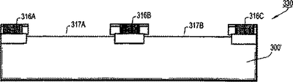
図14は、本発明の代表的な実施形態によるキャリア基板の構造を例示する。より具体的には、図14は、キャリア基板の非接合エリアからダミー・チップが除去された後のキャリア基板構造を示す。ここで図14を参照すると、ダミー・チップ(図示せず)が切断されキャリア基板300’から取り外された後、ポケット317Aおよび317Bならびにチップ間エリア311に前もって作られた有用なデバイス316A、316B、および316Cを含む構造330が形成される。
FIG. 14 illustrates the structure of a carrier substrate according to an exemplary embodiment of the present invention. More specifically, FIG. 14 shows the carrier substrate structure after the dummy chip is removed from the non-bonded area of the carrier substrate. Referring now to FIG. 14,
プロセス・ステップが同一であり、チップの厚さおよびポケットの深さは厳密に追跡されるので、ポケットおよびチップは、異なるウェハ上に異なる時点で、または異なるソースから、あるいはそれら両方において形成できることも留意されるべきである。チップをそれらの対応するポケット内に投入する前に、空隙302を満たすために、図3の誘電体層301と同じ厚さを有する誘電体層が設けられなければならない。好ましくは、空隙302は、チップをそれらの各々のポケット内に投入する前に、誘電体層、接着剤層、または熱ペーストで満たされる。結果として、すべてのチップがそれらの対応するポケット内に投入される場合、すべてのチップの最表面が、ポケットを有するウェハの最表面と実質的に同一平面であり、それによって、マルチチップ・ウェハレベル集積パッケージを形成するために必要とされるステップおよびプロセスの数が低減される。さらに、ダミー・キャリアのチップ間エリアに形成されたディスクリート・デバイスは、その上に形成されたチップの働きを試験および監視するために用いられる。それに対して、キャリア基板のチップ間エリアに形成されたディスクリート・デバイスは、マルチチップ・ウェハレベル・パッケージに一体化している部分である。
Since the process steps are the same and chip thickness and pocket depth are closely tracked, pockets and chips can also be formed on different wafers at different times, from different sources, or both. It should be noted. In order to fill the
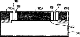
図15は、部分的ウェハ・ダイシング技術が実行された後の、図13に示されるチップの側面図である。図15を参照すると、薄化ウェハ層308の所定部分が部分的ウェハ・ダイシング技術を用いて除去され、それによって、キャリア基板300からチップ315Aを取り外す。加えて、チップ315Aの周囲にバッファ領域318が画定される。ダイシング技術が、薄化ウェハ層308を通って空隙302までダイシングすることによって実行され、それによって、基板からチップ315Aを取り外すことをさらに留意すべきである。言い換えれば、チップ315Aが空隙302において基板に取り付けられていないので、ひとたび薄化ウェハ層308がチップ315A周囲で切断およびダイシングされると、チップ315Aは取り外される。
FIG. 15 is a side view of the chip shown in FIG. 13 after a partial wafer dicing technique has been performed. Referring to FIG. 15, a predetermined portion of the thinned
図16は、部分的ウェハ・ダイシング技術が実行された後の、図13に示されるチップの平面図である。図16を参照すると、チップ315Aが、切断チャネル319に隣接するチップ315Aの外周に沿ってバッファ領域318を有しているのが示される。
FIG. 16 is a plan view of the chip shown in FIG. 13 after a partial wafer dicing technique has been performed. Referring to FIG. 16, the
図17(A)〜図17(C)は、本発明の代表的な実施形態による、キャリア基板上に形成されたチップを取り外すための方法を例示する。図17(A)において、厚さd1を有する薄いウェハ層510が、取り扱いおよび加工の間、機械的強度を維持するために、d2の厚さを有する、より厚い基板530に接合される。好ましくは、d1の厚さは、50μm〜300μmである。接合エリア521は、パターン形成された酸化物層540に接合されるウェハ層510により形成される。非接合エリア522は、酸化物層の欠如の結果生じる。チップ520、またはダイは、非接合エリア内の薄いウェハ層510中に形成される。しかしながら、ウェハ層510は、シリコン、ゲルマニウム、ガリウムヒ素、CdSe、II族元素とVI族元素との化合物、またはIII族元素とIV族元素との化合物であり得ることが留意されるべきである。部分的ウェハ・ダイシング技術は、薄いウェハ層510上にフォトレジスト・マスク500を形成し、そのフォトレジスト・マスク500をリソグラフィ露光することによって実行できる。フォトマスク500が画定された後、薄いウェハ層510をエッチングするために、ドライまたはウェット・エッチング・プロセスが実行される。代わりに、部分的ダイシングは、チップ520を取り外すために、マスクレス直接レーザ切断を用いて行うこともできる。図17(B)は、トレンチ550を示しており、このトレンチは、薄いウェハ層510を貫通しチップ520を取り囲んでいる非接合エリア522までエッチングすることによって形成される。図17(C)において、チップ520、またはダイは、非接合エリア522から除去され、それによって、ポケット560を形成する。トレンチ550をエッチングし、チップまたはダイを効果的に切断するために、高密度プラズマ、または反応性イオン・エッチングを用いることができる。同様に、ダミー・チップを基板から除去することによってポケットを形成できる。チップが取り付けられた後、チップの最表面がウェハの最表面と実質的に同一平面となるように、ポケットの深さは、現実のチップの厚さと実質的に同じ厚さを有するべきである。この方法を実行することにより、パッケージは、接合チップの最表面を平坦化するなどのどのような準備も必要とせずに、グローバル・チップ間(Chip−to−Chip)配線の用意ができている。
FIGS. 17A-17C illustrate a method for removing a chip formed on a carrier substrate, according to an exemplary embodiment of the present invention. In FIG. 17A, a thin wafer layer 510 having a thickness d1 is bonded to a
本発明の代表的な実施形態は、異なるプロセス・ステップおよび材料を用いて製造されたチップの集積を経済的な方法で容易にするマルチチップ・ウェハ・レベル・パッケージを形成するための方法を含む。図18は、本発明の代表的な実施形態による、マルチチップ・ウェハ・レベル・パッケージを形成するための方法を例示する流れ図である。ここで図18を参照すると、複数のチップがチップ基板上に形成される(ステップ602)。次に、キャリア基板からダミー・チップを取り外すことにより、キャリア基板中にポケットが形成される(ステップ604)。次に、チップは、チップ基板から取り外される(ステップ606)。ステップ604および606は、同時または異なる順序で実行できることが理解されるべきである。チップ基板から取り外されたチップは次に、チップの最表面がキャリア基板の最表面と実質的に同一平面になるようにキャリア基板中の所定のポケット内に取り付けられる(ステップ608)。
Exemplary embodiments of the present invention include a method for forming a multi-chip wafer level package that facilitates the integration of chips manufactured using different process steps and materials in an economical manner. . FIG. 18 is a flow diagram illustrating a method for forming a multichip wafer level package according to an exemplary embodiment of the present invention. Referring now to FIG. 18, a plurality of chips are formed on a chip substrate (step 602). Next, by removing the dummy chip from the carrier substrate, a pocket is formed in the carrier substrate (step 604). Next, the chip is removed from the chip substrate (step 606). It should be understood that
図19は、本発明の代表的な実施形態による、チップ基板上に複数のチップを形成するための方法を例示する流れ図である。特に、図19は、チップ基板上でのチップの形成に関する図18におけるステップ602の代表的な方法を例示する。ここで図19を参照すると、チップ基板上の誘電体層がパターン形成される(ステップ702)。次に、パターン形成された誘電体層は、オフチップ・エリアを画定するためにエッチングされる(ステップ704)。浅いトレンチ分離(STI)領域がオフチップ・エリア中に形成される(ステップ706)。次に、オフチップ・エリア間の誘電体層が除去される(ステップ708)。次に、STI領域に隣接しかつウェハとチップ基板との間に空隙が形成されるようにウェハがSTI領域に接合され、STI領域上方のウェハ中のエリアがチップ間エリアを画定し、空隙上方のエリアがチップ・エリアを画定する(ステップ710)。次に、ウェハが薄化される(ステップ712)。次に、薄化されたウェハ中にデバイスが形成される(ステップ714)。次に、デバイスがその中に形成された薄化されたウェハ上に後工程相互接続部が形成される(ステップ716)。最後に、薄化されたウェハのチップ・エリア中に最終仕上げデバイスおよび相互接続部が形成されてチップの形成を完了する(ステップ718)。さらに、上述のプロセスは、異なるチップ基板上において多くの異なるタイプのチップを形成するために使用できることが理解されるべきである。
FIG. 19 is a flow diagram illustrating a method for forming a plurality of chips on a chip substrate according to an exemplary embodiment of the present invention. In particular, FIG. 19 illustrates an exemplary method of
図20は、本発明の代表的な実施形態による、キャリア基板中に複数のポケットを形成するための方法を例示する流れ図である。特に、図20は、キャリア基板中でのポケットの形成に関する図18におけるステップ604の代表的な方法を例示する。ここで図20を参照すると、キャリア基板上の誘電体層がパターン形成される(ステップ802)。次に、パターン形成された誘電体層は、オフチップ・エリアを画定するためにエッチングされる(ステップ804)。次に、浅いトレンチ分離(STI)領域がオフチップエリア中に形成される(ステップ806)。次に、オフチップ・エリア間の誘電体層が除去される(ステップ808)。次に、STI領域に隣接しかつウェハとチップ基板との間に空隙が形成されるようにウェハがSTIに接合され、STI領域上方のウェハ中のエリアがチップ間エリアを画定し、空隙上方のエリアがチップ・エリアを画定する(ステップ810)。次に、ウェハが薄化される(ステップ812)。次に、薄化されたウェハ上に後工程相互接続部が形成される(ステップ814)。薄化されたウェハの最表面がパッシベーション層でコーティングされる(ステップ816)。次に、ウェハの所定の部分、またはダミー・チップが取り外され、ウェハのチップ・エリア中にチャネルをダイシングし、それによってウェハ内にポケットが形成される(ステップ818)。
FIG. 20 is a flow diagram illustrating a method for forming a plurality of pockets in a carrier substrate according to an exemplary embodiment of the present invention. In particular, FIG. 20 illustrates an exemplary method of
図21は、本発明の代表的な実施形態による、チップ基板からチップを取り外すための方法を例示する流れ図である。特に、図21は、チップ基板からのチップの取り外しに関する図18におけるステップ606の代表的な方法を例示する。ここで図21を参照すると、薄化されたウェハの最表面が、チップを保護するためにパッシベーション層でコーティングされる(ステップ902)。次に、ウェハのチップ・エリアを通り空隙までチャネルがダイシングされ、それによってチップ基板からチップを取り外す(ステップ904)。
FIG. 21 is a flow diagram illustrating a method for removing a chip from a chip substrate according to an exemplary embodiment of the present invention. In particular, FIG. 21 illustrates an exemplary method of
図22は、本発明の代表的な実施形態による、チップ基板から取り外されたチップをキャリア基板中の所定のポケット内に取り付けるための方法を例示する流れ図である。特に、図22は、図18におけるステップ608の代表的な方法を例示する。ここで図22を参照すると、空隙と同じ厚さを有する接着剤層または熱ペーストが、ポケットの底部分に設けられる(ステップ1002)。次に、チップがそれらの対応するポケット内に設置され、整列される(ステップ1004)。さらに、空隙と同じ寸法を有する誘電体層が接着剤層または熱ペーストの代わりに使用され得る。
FIG. 22 is a flow diagram illustrating a method for mounting a chip removed from a chip substrate in a predetermined pocket in a carrier substrate, according to an exemplary embodiment of the present invention. In particular, FIG. 22 illustrates an exemplary method of
要約すると、本発明の代表的な実施形態は、ウェハの表面にチップならびにポケットを形成するために、部分的ウェハ接合および部分的ウェハ・ダイシング技術が用いられる、コプラナー(共平面)マルチチップ・ウェハ・レベル・パッケージを形成するための効率的な方法を提供する。完成チップは、ウェハの対応するポケット内に取り付けられ、チップ間のグローバル相互接続部が、接合チップの一番上の平坦表面上に形成される。これらの方法は、異なるプロセス・ステップおよび材料で製造されたチップの集積を容易にする。チップの最表面を平坦化するために化学機械研磨のような過酷な平坦化プロセスを用いる必要は皆無である。チップは互いに正確に整列されており、すべてのチップが上向きに取り付けられているので、モジュールはグローバル配線の用意ができており、これにより、チップを上下逆の位置から裏返す必要がなくなる。 In summary, an exemplary embodiment of the present invention is a coplanar multi-chip wafer in which partial wafer bonding and partial wafer dicing techniques are used to form chips and pockets on the surface of the wafer. Provide an efficient way to form level packages. The finished chip is mounted in the corresponding pocket of the wafer and a global interconnect between the chips is formed on the top flat surface of the bonded chip. These methods facilitate the integration of chips manufactured with different process steps and materials. There is no need to use a harsh planarization process such as chemical mechanical polishing to planarize the outermost surface of the chip. Since the chips are precisely aligned with each other and all the chips are mounted upwards, the module is ready for global wiring, which eliminates the need to flip the chip upside down.
本発明を、本発明の代表的な実施形態に関連して具体的に示しかつ説明してきたが、以下の特許請求の範囲により定義される本発明の範囲を逸脱することなく、形状および詳細の種々の変更をその中で行い得ることが当業者により理解されるであろう。 Although the invention has been particularly shown and described in connection with exemplary embodiments thereof, it will be understood that the invention is not limited in form and detail without departing from the scope of the invention as defined by the following claims. It will be appreciated by those skilled in the art that various modifications can be made therein.
Claims (8)
複数のチップ基板上に複数の異種チップを形成するステップであって、前記複数のチップ基板の各々はただ1種のチップを形成するために用いられるステップと、
前記複数のチップ基板から前記複数の異種チップを取り外すステップと、
キャリア基板中にポケットを形成するステップであって、各々のポケットは前記異種チップの1つを保持するステップと、
前記複数のチップを前記キャリア基板中のそれらの対応するポケット内に、前記複数のチップの最表面が前記キャリア基板の最表面と実質的に同一平面になるように取り付けるステップとを含み、
複数のチップ基板上に複数のチップを形成する前記ステップは、ウェハを各チップ基板中の浅いトレンチ分離(STI)領域に、前記STI領域に隣接しかつ前記ウェハとチップ基板との間に空隙が形成されるように接合するステップを含み、前記STI領域上方の前記ウェハ中のエリアがチップ間エリアを画定し、前記空隙上方の前記ウェハ中のエリアがチップ・エリアを画定し、
前記チップ基板の前記チップ間エリア中にディスクリート・デバイスを形成するステップをさらに含み、
前記複数のチップとは、
前記複数の異種のチップのうちの複数の互いに異なる種類のチップ、又は、複数の互いに異なる種類のチップと複数の同じ種類のチップの両方である、方法。 A method of forming a multichip wafer level package comprising:
Forming a plurality of different types of chips on a plurality of chip substrates, each of the plurality of chip substrates being used to form only one type of chip;
Removing the plurality of different types of chips from the plurality of chip substrates;
Forming pockets in the carrier substrate, each pocket holding one of the dissimilar chips;
Mounting the plurality of chips in their corresponding pockets in the carrier substrate such that the outermost surface of the plurality of chips is substantially flush with the outermost surface of the carrier substrate;
The step of forming a plurality of chips on a plurality of chip substrates includes the step of forming a wafer in a shallow trench isolation (STI) region in each chip substrate, adjacent to the STI region and between the wafer and the chip substrate. Bonding to form an area in the wafer above the STI region defining an inter-chip area, and an area in the wafer above the air gap defining a chip area;
Further seen including a step of forming a discrete device in said inter-chip areas of the chip substrate,
The plurality of chips is
A plurality of different types of chips from the plurality of different types of chips, or a plurality of different types of chips and a plurality of the same type of chips .
複数のチップ基板上に複数の異種チップを形成するステップであって、前記複数のチップ基板の各々はただ1種のチップを形成するために用いられるステップと、
前記複数のチップ基板から前記複数の異種チップを取り外すステップと、
キャリア基板中にポケットを形成するステップであって、各々のポケットは前記異種チップの1つを保持するステップと、
前記複数のチップを前記キャリア基板中のそれらの対応するポケット内に、前記複数のチップの最表面が前記キャリア基板の最表面と実質的に同一平面になるように取り付けるステップとを含み、
複数のチップ基板上に複数のチップを形成する前記ステップは、ウェハを各チップ基板中の浅いトレンチ分離(STI)領域に、前記STI領域に隣接しかつ前記ウェハとチップ基板との間に空隙が形成されるように接合するステップを含み、前記STI領域上方の前記ウェハ中のエリアがチップ間エリアを画定し、前記空隙上方の前記ウェハ中のエリアがチップ・エリアを画定し、
前記チップ基板の前記チップ間エリアに形成されるデバイスは、前記空隙情報のウェハ中に形成されるデバイスの試験及び監視のためにのみ用いられ、
前記複数のチップとは、前記複数の異種のチップのうちの複数の互いに異なる種類のチップ、又は、複数の互いに異なる種類のチップと複数の同じ種類のチップの両方のいずれかである、方法。 A method of forming a multichip wafer level package comprising:
Forming a plurality of different types of chips on a plurality of chip substrates, each of the plurality of chip substrates being used to form only one type of chip;
Removing the plurality of different types of chips from the plurality of chip substrates;
Forming pockets in the carrier substrate, each pocket holding one of the dissimilar chips;
Mounting the plurality of chips in their corresponding pockets in the carrier substrate such that the outermost surface of the plurality of chips is substantially flush with the outermost surface of the carrier substrate;
The step of forming a plurality of chips on a plurality of chip substrates includes the step of forming a wafer in a shallow trench isolation (STI) region in each chip substrate, adjacent to the STI region and between the wafer and the chip substrate. Bonding to form an area in the wafer above the STI region defining an inter-chip area, and an area in the wafer above the air gap defining a chip area;
Devices formed in the inter-chip area of the chip substrate are used only for testing and monitoring of devices formed in the gap information wafer ,
The plurality of chips are either a plurality of different types of chips of the plurality of different types of chips, or a plurality of different types of chips and a plurality of the same type of chips .
前記チップ基板上に誘電体層をパターン形成するステップと、
オフチップ・エリアを画定するために前記パターン形成された誘電体層をエッチングするステップと、
前記オフチップ・エリア中にSTI領域を形成するステップと、
前記オフチップ・エリアの間の前記誘電体層を除去するステップとを含む、
請求項1または2に記載の方法。 Prior to the step of bonding the wafer to the STI region,
Patterning a dielectric layer on the chip substrate;
Etching the patterned dielectric layer to define off-chip areas;
Forming an STI region in the off-chip area;
Removing the dielectric layer between the off-chip areas.
The method according to claim 1 or 2.
前記薄化されたウェハ中にデバイスを形成するステップと、
前記薄化されたウェハ上に後工程(BEOL)相互接続部を形成するステップと、
前記チップ・エリア中に最終仕上げデバイスおよび相互接続部を形成して、前記複数のチップの形成を完了するステップとをさらに含む、請求項1または2に記載の方法。 Thinning the wafer;
Forming a device in the thinned wafer;
Forming a post-process (BEOL) interconnect on the thinned wafer;
Forming a final finishing device and interconnects in the chip area to complete the formation of the plurality of chips.
前記薄化されたウェハの最表面をパッシベーション層でコーティングするステップと
前記薄化されたウェハの前記チップ・エリアを通り前記空隙までチャネルをダイシングし、それによって前記複数のチップを前記複数のチップ基板から取り外すステップとを含む、請求項4に記載の方法。 The step of removing the plurality of chips from the plurality of chip substrates includes:
Coating the outermost surface of the thinned wafer with a passivation layer; dicing a channel through the chip area of the thinned wafer to the gap, thereby causing the plurality of chips to become the plurality of chip substrates. 5. The method of claim 4, comprising the step of removing from.
チップ基板中に浅いトレンチ分離(STI)領域を形成するステップと、
ウェハを前記チップ基板中のSTI領域に、前記STI領域に隣接しかつ前記ウェハと前記チップ基板との間に空隙が形成されるように接合するステップであって、前記STI領域上方の前記ウェハ中のエリアはチップ間エリアを画定し、前記空隙上方の前記ウェハ中のエリアはチップ・エリアを画定するステップと、
前記ウェハを薄化するステップと、
前記薄化されたウェハ中にデバイスを形成するステップと、
前記薄化されたウェハ上に後工程(BEOL)相互接続部を形成するステップと、
前記チップ・エリア中に最終仕上げデバイスおよび相互接続部を形成し、複数のチップの前記形成を完了するステップとを含み、
前記チップ基板の前記チップ間エリア中にディスクリート・デバイスを形成するステップをさらに含む、方法。 A method of forming a multichip wafer level package comprising:
Forming a shallow trench isolation (STI) region in the chip substrate;
Bonding a wafer to an STI region in the chip substrate such that a gap is formed adjacent to the STI region and between the wafer and the chip substrate, wherein the wafer is in the wafer above the STI region; The area of the wafer defines an inter-chip area, and the area in the wafer above the gap defines a chip area;
Thinning the wafer;
Forming a device in the thinned wafer;
Forming a post-process (BEOL) interconnect on the thinned wafer;
Forming a final finishing device and interconnects in the chip area and completing the formation of a plurality of chips;
Forming a discrete device in the inter-chip area of the chip substrate.
前記薄化されたウェハの前記チップ・エリアを通り前記空隙までチャネルをダイシングし、それによって前記複数のチップを前記複数のチップ基板から取り外すステップとをさらに含む、請求項6に記載の方法。 Coating the outermost surface of the thinned wafer with a passivation layer; dicing a channel through the chip area of the thinned wafer to the gap, thereby causing the plurality of chips to become the plurality of chip substrates. 7. The method of claim 6, further comprising the step of removing from.
Applications Claiming Priority (2)
| Application Number | Priority Date | Filing Date | Title |
|---|---|---|---|
| US10/994,494 | 2004-11-20 | ||
| US10/994,494 US7405108B2 (en) | 2004-11-20 | 2004-11-20 | Methods for forming co-planar wafer-scale chip packages |
Related Parent Applications (1)
| Application Number | Title | Priority Date | Filing Date |
|---|---|---|---|
| JP2007541952A Division JP5459959B2 (en) | 2004-11-20 | 2005-11-16 | Method for forming a multi-chip wafer level package |
Publications (2)
| Publication Number | Publication Date |
|---|---|
| JP2011249830A JP2011249830A (en) | 2011-12-08 |
| JP5474002B2 true JP5474002B2 (en) | 2014-04-16 |
Family
ID=35735294
Family Applications (2)
| Application Number | Title | Priority Date | Filing Date |
|---|---|---|---|
| JP2007541952A Expired - Fee Related JP5459959B2 (en) | 2004-11-20 | 2005-11-16 | Method for forming a multi-chip wafer level package |
| JP2011160519A Expired - Fee Related JP5474002B2 (en) | 2004-11-20 | 2011-07-22 | Method for forming a multi-chip wafer level package |
Family Applications Before (1)
| Application Number | Title | Priority Date | Filing Date |
|---|---|---|---|
| JP2007541952A Expired - Fee Related JP5459959B2 (en) | 2004-11-20 | 2005-11-16 | Method for forming a multi-chip wafer level package |
Country Status (9)
| Country | Link |
|---|---|
| US (2) | US7405108B2 (en) |
| EP (1) | EP1817793B1 (en) |
| JP (2) | JP5459959B2 (en) |
| KR (1) | KR100992015B1 (en) |
| CN (1) | CN100437952C (en) |
| AT (1) | ATE477588T1 (en) |
| DE (1) | DE602005022919D1 (en) |
| TW (1) | TWI362706B (en) |
| WO (1) | WO2006053879A1 (en) |
Families Citing this family (26)
| Publication number | Priority date | Publication date | Assignee | Title |
|---|---|---|---|---|
| US7405108B2 (en) * | 2004-11-20 | 2008-07-29 | International Business Machines Corporation | Methods for forming co-planar wafer-scale chip packages |
| US7442579B2 (en) * | 2004-11-22 | 2008-10-28 | International Business Machines Corporation | Methods to achieve precision alignment for wafer scale packages |
| DE102005039479B3 (en) * | 2005-08-18 | 2007-03-29 | Infineon Technologies Ag | Semiconductor device with thinned semiconductor chip and method for producing the thinned semiconductor device |
| US7658901B2 (en) * | 2005-10-14 | 2010-02-09 | The Trustees Of Princeton University | Thermally exfoliated graphite oxide |
| JP4559993B2 (en) * | 2006-03-29 | 2010-10-13 | 株式会社東芝 | Manufacturing method of semiconductor device |
| KR100829392B1 (en) * | 2006-08-24 | 2008-05-13 | 동부일렉트로닉스 주식회사 | Method of fabricating SoC |
| TW200941661A (en) * | 2008-03-19 | 2009-10-01 | Integrated Circuit Solution Inc | Shape of window formed in a substrate for window ball grid array package |
| JP4828559B2 (en) * | 2008-03-24 | 2011-11-30 | 新光電気工業株式会社 | Wiring board manufacturing method and electronic device manufacturing method |
| US8772087B2 (en) * | 2009-10-22 | 2014-07-08 | Infineon Technologies Ag | Method and apparatus for semiconductor device fabrication using a reconstituted wafer |
| US8322022B1 (en) | 2010-06-28 | 2012-12-04 | Western Digital (Fremont), Llc | Method for providing an energy assisted magnetic recording head in a wafer packaging configuration |
| CN102386088B (en) * | 2010-09-03 | 2014-06-25 | 中芯国际集成电路制造(上海)有限公司 | Method for removing photoinduced resist layer on semiconductor device structure |
| CN102769002B (en) * | 2011-04-30 | 2016-09-14 | 中国科学院微电子研究所 | Semiconductor device and forming method thereof, encapsulating structure |
| JP6063641B2 (en) * | 2012-05-16 | 2017-01-18 | 株式会社ディスコ | Wafer protection member |
| US20150380369A1 (en) * | 2013-09-30 | 2015-12-31 | Nantong Fujitsu Microelectronics Co., Ltd | Wafer packaging structure and packaging method |
| US9123546B2 (en) | 2013-11-14 | 2015-09-01 | Taiwan Semiconductor Manufacturing Company Limited | Multi-layer semiconductor device structures with different channel materials |
| US9350339B2 (en) | 2014-07-18 | 2016-05-24 | Qualcomm Incorporated | Systems and methods for clock distribution in a die-to-die interface |
| JP6341959B2 (en) * | 2016-05-27 | 2018-06-13 | 浜松ホトニクス株式会社 | Manufacturing method of Fabry-Perot interference filter |
| US11041755B2 (en) | 2016-05-27 | 2021-06-22 | Hamamatsu Photonics K.K. | Production method for Fabry-Perot interference filter |
| CN109477958A (en) | 2016-08-24 | 2019-03-15 | 浜松光子学株式会社 | Fabry-Perot interference optical filter |
| US10916507B2 (en) | 2018-12-04 | 2021-02-09 | International Business Machines Corporation | Multiple chip carrier for bridge assembly |
| GB2582382B (en) * | 2019-03-22 | 2023-10-25 | Cirrus Logic Int Semiconductor Ltd | Semiconductor structures |
| US11456247B2 (en) * | 2019-06-13 | 2022-09-27 | Nanya Technology Corporation | Semiconductor device and fabrication method for the same |
| CN110690868B (en) * | 2019-09-27 | 2021-02-19 | 无锡市好达电子股份有限公司 | Novel wafer-level packaging method for filter |
| CN111128716B (en) * | 2019-11-15 | 2023-10-17 | 西安电子科技大学 | Heterogeneous integration method for large-area graph self-alignment |
| KR20210120221A (en) | 2020-03-26 | 2021-10-07 | 삼성전자주식회사 | Semiconductor stack and manufacturing method thereof |
| TWI790003B (en) * | 2021-11-18 | 2023-01-11 | 佳邦科技股份有限公司 | Over-voltage protection device |
Family Cites Families (21)
| Publication number | Priority date | Publication date | Assignee | Title |
|---|---|---|---|---|
| JPS6281745A (en) | 1985-10-05 | 1987-04-15 | Fujitsu Ltd | Lsi semiconductor device in wafer scale and manufacture thereof |
| US4866501A (en) * | 1985-12-16 | 1989-09-12 | American Telephone And Telegraph Company At&T Bell Laboratories | Wafer scale integration |
| US5091331A (en) | 1990-04-16 | 1992-02-25 | Harris Corporation | Ultra-thin circuit fabrication by controlled wafer debonding |
| JPH0645436A (en) * | 1992-07-22 | 1994-02-18 | Nec Corp | Bonding method for semiconductor substrate |
| US5324687A (en) * | 1992-10-16 | 1994-06-28 | General Electric Company | Method for thinning of integrated circuit chips for lightweight packaged electronic systems |
| JPH0878487A (en) * | 1994-08-31 | 1996-03-22 | Nec Kyushu Ltd | Semiconductor substrate and fabrication of semiconductor |
| US5770884A (en) * | 1995-06-30 | 1998-06-23 | International Business Machines Corporation | Very dense integrated circuit package |
| US5880007A (en) * | 1997-09-30 | 1999-03-09 | Siemens Aktiengesellschaft | Planarization of a non-conformal device layer in semiconductor fabrication |
| US6177299B1 (en) * | 1998-01-15 | 2001-01-23 | International Business Machines Corporation | Transistor having substantially isolated body and method of making the same |
| JPH11354667A (en) * | 1998-06-05 | 1999-12-24 | Nippon Telegr & Teleph Corp <Ntt> | Electronic part and its mounting method |
| US6627477B1 (en) * | 2000-09-07 | 2003-09-30 | International Business Machines Corporation | Method of assembling a plurality of semiconductor devices having different thickness |
| US6555906B2 (en) * | 2000-12-15 | 2003-04-29 | Intel Corporation | Microelectronic package having a bumpless laminated interconnection layer |
| FR2823596B1 (en) * | 2001-04-13 | 2004-08-20 | Commissariat Energie Atomique | SUBSTRATE OR DISMOUNTABLE STRUCTURE AND METHOD OF MAKING SAME |
| JP2003197850A (en) * | 2001-12-26 | 2003-07-11 | Sony Corp | Semiconductor device and method of manufacturing the same |
| JP4260405B2 (en) * | 2002-02-08 | 2009-04-30 | 株式会社ルネサステクノロジ | Manufacturing method of semiconductor integrated circuit device |
| US7203393B2 (en) * | 2002-03-08 | 2007-04-10 | Movaz Networks, Inc. | MEMS micro mirrors driven by electrodes fabricated on another substrate |
| DE60335554D1 (en) * | 2002-05-20 | 2011-02-10 | Imagerlabs Inc | FORMING AN INTEGRATED MULTIPLE ENGINEERING WITH INSULATED SUBSTRATES |
| US6964881B2 (en) * | 2002-08-27 | 2005-11-15 | Micron Technology, Inc. | Multi-chip wafer level system packages and methods of forming same |
| US7078320B2 (en) * | 2004-08-10 | 2006-07-18 | International Business Machines Corporation | Partial wafer bonding and dicing |
| US7005319B1 (en) * | 2004-11-19 | 2006-02-28 | International Business Machines Corporation | Global planarization of wafer scale package with precision die thickness control |
| US7405108B2 (en) * | 2004-11-20 | 2008-07-29 | International Business Machines Corporation | Methods for forming co-planar wafer-scale chip packages |
-
2004
- 2004-11-20 US US10/994,494 patent/US7405108B2/en active Active
-
2005
- 2005-11-16 EP EP05808156A patent/EP1817793B1/en not_active Not-in-force
- 2005-11-16 KR KR1020077011373A patent/KR100992015B1/en not_active IP Right Cessation
- 2005-11-16 WO PCT/EP2005/056009 patent/WO2006053879A1/en active Application Filing
- 2005-11-16 AT AT05808156T patent/ATE477588T1/en not_active IP Right Cessation
- 2005-11-16 CN CNB2005800325958A patent/CN100437952C/en active Active
- 2005-11-16 JP JP2007541952A patent/JP5459959B2/en not_active Expired - Fee Related
- 2005-11-16 DE DE602005022919T patent/DE602005022919D1/en active Active
- 2005-11-17 TW TW094140468A patent/TWI362706B/en not_active IP Right Cessation
-
2008
- 2008-05-15 US US12/121,468 patent/US7867820B2/en not_active Expired - Fee Related
-
2011
- 2011-07-22 JP JP2011160519A patent/JP5474002B2/en not_active Expired - Fee Related
Also Published As
| Publication number | Publication date |
|---|---|
| US7405108B2 (en) | 2008-07-29 |
| US20060110851A1 (en) | 2006-05-25 |
| KR100992015B1 (en) | 2010-11-05 |
| DE602005022919D1 (en) | 2010-09-23 |
| ATE477588T1 (en) | 2010-08-15 |
| KR20070085402A (en) | 2007-08-27 |
| CN100437952C (en) | 2008-11-26 |
| WO2006053879A1 (en) | 2006-05-26 |
| TW200633081A (en) | 2006-09-16 |
| CN101027765A (en) | 2007-08-29 |
| EP1817793A1 (en) | 2007-08-15 |
| US7867820B2 (en) | 2011-01-11 |
| JP2011249830A (en) | 2011-12-08 |
| EP1817793B1 (en) | 2010-08-11 |
| US20080280399A1 (en) | 2008-11-13 |
| JP2008521228A (en) | 2008-06-19 |
| TWI362706B (en) | 2012-04-21 |
| JP5459959B2 (en) | 2014-04-02 |
Similar Documents
| Publication | Publication Date | Title |
|---|---|---|
| JP5474002B2 (en) | Method for forming a multi-chip wafer level package | |
| US10011098B2 (en) | Four D device process and structure | |
| JP3986575B2 (en) | Manufacturing method of three-dimensional integrated circuit | |
| US7098070B2 (en) | Device and method for fabricating double-sided SOI wafer scale package with through via connections | |
| TWI478282B (en) | Method for stacking semiconductor dies | |
| US7528494B2 (en) | Accessible chip stack and process of manufacturing thereof | |
| US7642173B2 (en) | Three-dimensional face-to-face integration assembly | |
| US7170164B2 (en) | Cooling system for a semiconductor device and method of fabricating same | |
| US6242778B1 (en) | Cooling method for silicon on insulator devices | |
| JP2008521228A5 (en) | ||
| WO2019062241A1 (en) | Wafer-level system packaging method and packaging structure | |
| US20080079152A1 (en) | Semiconductor wafer and method of manufacturing the same and method of manufacturing semiconductor device | |
| JPH08204123A (en) | Preparation of three-dimensional integrated circuit | |
| US11164840B2 (en) | Chip interconnection structure, wafer interconnection structure and method for manufacturing the same | |
| EP3171399B1 (en) | Method for singulating a stack of semiconductor wafers | |
| US10818570B1 (en) | Stacked semiconductor devices having dissimilar-sized dies | |
| US20240038686A1 (en) | Semiconductor packages and methods of manufacturing thereof | |
| WO2022252087A1 (en) | Method of manufacturing active reconstructed wafers |
Legal Events
| Date | Code | Title | Description |
|---|---|---|---|
| A977 | Report on retrieval |
Free format text: JAPANESE INTERMEDIATE CODE: A971007 Effective date: 20130212 |
|
| A131 | Notification of reasons for refusal |
Free format text: JAPANESE INTERMEDIATE CODE: A131 Effective date: 20130219 |
|
| A521 | Request for written amendment filed |
Free format text: JAPANESE INTERMEDIATE CODE: A523 Effective date: 20130502 |
|
| RD12 | Notification of acceptance of power of sub attorney |
Free format text: JAPANESE INTERMEDIATE CODE: A7432 Effective date: 20130502 |
|
| A521 | Request for written amendment filed |
Free format text: JAPANESE INTERMEDIATE CODE: A821 Effective date: 20130503 |
|
| TRDD | Decision of grant or rejection written | ||
| A01 | Written decision to grant a patent or to grant a registration (utility model) |
Free format text: JAPANESE INTERMEDIATE CODE: A01 Effective date: 20140115 |
|
| A61 | First payment of annual fees (during grant procedure) |
Free format text: JAPANESE INTERMEDIATE CODE: A61 Effective date: 20140204 |
|
| R150 | Certificate of patent or registration of utility model |
Free format text: JAPANESE INTERMEDIATE CODE: R150 |
|
| R250 | Receipt of annual fees |
Free format text: JAPANESE INTERMEDIATE CODE: R250 |
|
| LAPS | Cancellation because of no payment of annual fees |