JP5460984B2 - Method for manufacturing semiconductor device - Google Patents
Method for manufacturing semiconductor device Download PDFInfo
- Publication number
- JP5460984B2 JP5460984B2 JP2008203852A JP2008203852A JP5460984B2 JP 5460984 B2 JP5460984 B2 JP 5460984B2 JP 2008203852 A JP2008203852 A JP 2008203852A JP 2008203852 A JP2008203852 A JP 2008203852A JP 5460984 B2 JP5460984 B2 JP 5460984B2
- Authority
- JP
- Japan
- Prior art keywords
- semiconductor film
- substrate
- semiconductor
- film
- bond substrate
- Prior art date
- Legal status (The legal status is an assumption and is not a legal conclusion. Google has not performed a legal analysis and makes no representation as to the accuracy of the status listed.)
- Expired - Fee Related
Links
- 239000004065 semiconductor Substances 0.000 title claims description 562
- 238000000034 method Methods 0.000 title claims description 89
- 238000004519 manufacturing process Methods 0.000 title claims description 75
- 239000000758 substrate Substances 0.000 claims description 408
- 230000007547 defect Effects 0.000 claims description 68
- 239000013078 crystal Substances 0.000 claims description 41
- 238000005530 etching Methods 0.000 claims description 31
- 238000010438 heat treatment Methods 0.000 claims description 30
- 230000001678 irradiating effect Effects 0.000 claims description 13
- 239000010408 film Substances 0.000 description 655
- 239000002585 base Substances 0.000 description 99
- 239000010410 layer Substances 0.000 description 97
- 239000007789 gas Substances 0.000 description 67
- 239000001257 hydrogen Substances 0.000 description 51
- 229910052739 hydrogen Inorganic materials 0.000 description 51
- 239000012535 impurity Substances 0.000 description 49
- 229910052710 silicon Inorganic materials 0.000 description 42
- XUIMIQQOPSSXEZ-UHFFFAOYSA-N Silicon Chemical compound [Si] XUIMIQQOPSSXEZ-UHFFFAOYSA-N 0.000 description 41
- 239000010703 silicon Substances 0.000 description 41
- -1 hydrogen ions Chemical class 0.000 description 35
- UFHFLCQGNIYNRP-UHFFFAOYSA-N Hydrogen Chemical compound [H][H] UFHFLCQGNIYNRP-UHFFFAOYSA-N 0.000 description 32
- 229910052581 Si3N4 Inorganic materials 0.000 description 32
- HQVNEWCFYHHQES-UHFFFAOYSA-N silicon nitride Chemical compound N12[Si]34N5[Si]62N3[Si]51N64 HQVNEWCFYHHQES-UHFFFAOYSA-N 0.000 description 32
- VYPSYNLAJGMNEJ-UHFFFAOYSA-N Silicium dioxide Chemical compound O=[Si]=O VYPSYNLAJGMNEJ-UHFFFAOYSA-N 0.000 description 25
- 229910052814 silicon oxide Inorganic materials 0.000 description 23
- 150000002500 ions Chemical class 0.000 description 22
- 229920005989 resin Polymers 0.000 description 22
- 239000011347 resin Substances 0.000 description 22
- 230000001070 adhesive effect Effects 0.000 description 19
- 239000000701 coagulant Substances 0.000 description 19
- 229910052760 oxygen Inorganic materials 0.000 description 19
- 239000001301 oxygen Substances 0.000 description 19
- IJGRMHOSHXDMSA-UHFFFAOYSA-N Atomic nitrogen Chemical compound N#N IJGRMHOSHXDMSA-UHFFFAOYSA-N 0.000 description 18
- QVGXLLKOCUKJST-UHFFFAOYSA-N atomic oxygen Chemical compound [O] QVGXLLKOCUKJST-UHFFFAOYSA-N 0.000 description 18
- 239000010936 titanium Substances 0.000 description 18
- 229910052782 aluminium Inorganic materials 0.000 description 17
- 238000000926 separation method Methods 0.000 description 16
- BLRPTPMANUNPDV-UHFFFAOYSA-N Silane Chemical compound [SiH4] BLRPTPMANUNPDV-UHFFFAOYSA-N 0.000 description 15
- XAGFODPZIPBFFR-UHFFFAOYSA-N aluminium Chemical compound [Al] XAGFODPZIPBFFR-UHFFFAOYSA-N 0.000 description 15
- 229910000077 silane Inorganic materials 0.000 description 15
- QGZKDVFQNNGYKY-UHFFFAOYSA-N Ammonia Chemical compound N QGZKDVFQNNGYKY-UHFFFAOYSA-N 0.000 description 14
- 239000000969 carrier Substances 0.000 description 14
- 230000001133 acceleration Effects 0.000 description 13
- 229910052751 metal Inorganic materials 0.000 description 13
- 239000002184 metal Substances 0.000 description 13
- 229910052719 titanium Inorganic materials 0.000 description 13
- MWUXSHHQAYIFBG-UHFFFAOYSA-N Nitric oxide Chemical compound O=[N] MWUXSHHQAYIFBG-UHFFFAOYSA-N 0.000 description 12
- BOTDANWDWHJENH-UHFFFAOYSA-N Tetraethyl orthosilicate Chemical compound CCO[Si](OCC)(OCC)OCC BOTDANWDWHJENH-UHFFFAOYSA-N 0.000 description 12
- RTAQQCXQSZGOHL-UHFFFAOYSA-N Titanium Chemical compound [Ti] RTAQQCXQSZGOHL-UHFFFAOYSA-N 0.000 description 12
- 239000011521 glass Substances 0.000 description 12
- 239000000203 mixture Substances 0.000 description 12
- 238000005268 plasma chemical vapour deposition Methods 0.000 description 12
- PXHVJJICTQNCMI-UHFFFAOYSA-N Nickel Chemical compound [Ni] PXHVJJICTQNCMI-UHFFFAOYSA-N 0.000 description 11
- CSDREXVUYHZDNP-UHFFFAOYSA-N alumanylidynesilicon Chemical compound [Al].[Si] CSDREXVUYHZDNP-UHFFFAOYSA-N 0.000 description 11
- 238000003776 cleavage reaction Methods 0.000 description 11
- 239000000463 material Substances 0.000 description 11
- 230000007017 scission Effects 0.000 description 11
- 239000000853 adhesive Substances 0.000 description 10
- 230000004888 barrier function Effects 0.000 description 10
- 229920001940 conductive polymer Polymers 0.000 description 10
- 239000004973 liquid crystal related substance Substances 0.000 description 10
- 230000015572 biosynthetic process Effects 0.000 description 9
- KPUWHANPEXNPJT-UHFFFAOYSA-N disiloxane Chemical class [SiH3]O[SiH3] KPUWHANPEXNPJT-UHFFFAOYSA-N 0.000 description 9
- 229910052757 nitrogen Inorganic materials 0.000 description 9
- 238000009832 plasma treatment Methods 0.000 description 9
- 238000005229 chemical vapour deposition Methods 0.000 description 8
- 150000001875 compounds Chemical class 0.000 description 8
- 238000005984 hydrogenation reaction Methods 0.000 description 8
- 229910052750 molybdenum Inorganic materials 0.000 description 8
- 239000011733 molybdenum Substances 0.000 description 8
- 239000000126 substance Substances 0.000 description 8
- 229910052721 tungsten Inorganic materials 0.000 description 8
- ZOKXTWBITQBERF-UHFFFAOYSA-N Molybdenum Chemical compound [Mo] ZOKXTWBITQBERF-UHFFFAOYSA-N 0.000 description 7
- 229910021529 ammonia Inorganic materials 0.000 description 7
- 238000000137 annealing Methods 0.000 description 7
- 230000006870 function Effects 0.000 description 7
- BASFCYQUMIYNBI-UHFFFAOYSA-N platinum Chemical compound [Pt] BASFCYQUMIYNBI-UHFFFAOYSA-N 0.000 description 7
- 238000005498 polishing Methods 0.000 description 7
- 238000007789 sealing Methods 0.000 description 7
- 239000002904 solvent Substances 0.000 description 7
- 239000010937 tungsten Substances 0.000 description 7
- WZJUBBHODHNQPW-UHFFFAOYSA-N 2,4,6,8-tetramethyl-1,3,5,7,2$l^{3},4$l^{3},6$l^{3},8$l^{3}-tetraoxatetrasilocane Chemical compound C[Si]1O[Si](C)O[Si](C)O[Si](C)O1 WZJUBBHODHNQPW-UHFFFAOYSA-N 0.000 description 6
- 229910000577 Silicon-germanium Inorganic materials 0.000 description 6
- NRTOMJZYCJJWKI-UHFFFAOYSA-N Titanium nitride Chemical compound [Ti]#N NRTOMJZYCJJWKI-UHFFFAOYSA-N 0.000 description 6
- XLOMVQKBTHCTTD-UHFFFAOYSA-N Zinc monoxide Chemical compound [Zn]=O XLOMVQKBTHCTTD-UHFFFAOYSA-N 0.000 description 6
- LEVVHYCKPQWKOP-UHFFFAOYSA-N [Si].[Ge] Chemical compound [Si].[Ge] LEVVHYCKPQWKOP-UHFFFAOYSA-N 0.000 description 6
- 229910052784 alkaline earth metal Inorganic materials 0.000 description 6
- 150000001342 alkaline earth metals Chemical class 0.000 description 6
- 229910045601 alloy Inorganic materials 0.000 description 6
- 239000000956 alloy Substances 0.000 description 6
- 239000010949 copper Substances 0.000 description 6
- 238000010586 diagram Methods 0.000 description 6
- 230000008014 freezing Effects 0.000 description 6
- 238000007710 freezing Methods 0.000 description 6
- 229910052732 germanium Inorganic materials 0.000 description 6
- GNPVGFCGXDBREM-UHFFFAOYSA-N germanium atom Chemical compound [Ge] GNPVGFCGXDBREM-UHFFFAOYSA-N 0.000 description 6
- 230000003287 optical effect Effects 0.000 description 6
- 150000002894 organic compounds Chemical class 0.000 description 6
- 229920001721 polyimide Polymers 0.000 description 6
- 239000002356 single layer Substances 0.000 description 6
- CZDYPVPMEAXLPK-UHFFFAOYSA-N tetramethylsilane Chemical compound C[Si](C)(C)C CZDYPVPMEAXLPK-UHFFFAOYSA-N 0.000 description 6
- WFKWXMTUELFFGS-UHFFFAOYSA-N tungsten Chemical compound [W] WFKWXMTUELFFGS-UHFFFAOYSA-N 0.000 description 6
- 238000007740 vapor deposition Methods 0.000 description 6
- JBRZTFJDHDCESZ-UHFFFAOYSA-N AsGa Chemical compound [As]#[Ga] JBRZTFJDHDCESZ-UHFFFAOYSA-N 0.000 description 5
- 229910001218 Gallium arsenide Inorganic materials 0.000 description 5
- GPXJNWSHGFTCBW-UHFFFAOYSA-N Indium phosphide Chemical compound [In]#P GPXJNWSHGFTCBW-UHFFFAOYSA-N 0.000 description 5
- 239000004642 Polyimide Substances 0.000 description 5
- 229910052783 alkali metal Inorganic materials 0.000 description 5
- 150000001340 alkali metals Chemical class 0.000 description 5
- 238000006243 chemical reaction Methods 0.000 description 5
- 239000011651 chromium Substances 0.000 description 5
- 230000002950 deficient Effects 0.000 description 5
- 229910052759 nickel Inorganic materials 0.000 description 5
- 150000001282 organosilanes Chemical class 0.000 description 5
- 229920001707 polybutylene terephthalate Polymers 0.000 description 5
- 229920000139 polyethylene terephthalate Polymers 0.000 description 5
- 239000005020 polyethylene terephthalate Substances 0.000 description 5
- 229910021332 silicide Inorganic materials 0.000 description 5
- FVBUAEGBCNSCDD-UHFFFAOYSA-N silicide(4-) Chemical compound [Si-4] FVBUAEGBCNSCDD-UHFFFAOYSA-N 0.000 description 5
- 238000004544 sputter deposition Methods 0.000 description 5
- 229910052715 tantalum Inorganic materials 0.000 description 5
- GUVRBAGPIYLISA-UHFFFAOYSA-N tantalum atom Chemical compound [Ta] GUVRBAGPIYLISA-UHFFFAOYSA-N 0.000 description 5
- ZOXJGFHDIHLPTG-UHFFFAOYSA-N Boron Chemical compound [B] ZOXJGFHDIHLPTG-UHFFFAOYSA-N 0.000 description 4
- 239000004696 Poly ether ether ketone Substances 0.000 description 4
- 239000004697 Polyetherimide Substances 0.000 description 4
- 238000010521 absorption reaction Methods 0.000 description 4
- 238000004458 analytical method Methods 0.000 description 4
- 239000012298 atmosphere Substances 0.000 description 4
- 229910052796 boron Inorganic materials 0.000 description 4
- 239000000919 ceramic Substances 0.000 description 4
- 238000000576 coating method Methods 0.000 description 4
- 239000004020 conductor Substances 0.000 description 4
- 230000005281 excited state Effects 0.000 description 4
- 230000005283 ground state Effects 0.000 description 4
- 150000002431 hydrogen Chemical class 0.000 description 4
- AMGQUBHHOARCQH-UHFFFAOYSA-N indium;oxotin Chemical compound [In].[Sn]=O AMGQUBHHOARCQH-UHFFFAOYSA-N 0.000 description 4
- 238000002347 injection Methods 0.000 description 4
- 239000007924 injection Substances 0.000 description 4
- 239000011810 insulating material Substances 0.000 description 4
- 239000011368 organic material Substances 0.000 description 4
- 230000001590 oxidative effect Effects 0.000 description 4
- 229920003023 plastic Polymers 0.000 description 4
- 239000004033 plastic Substances 0.000 description 4
- 229920002492 poly(sulfone) Polymers 0.000 description 4
- 229920001230 polyarylate Polymers 0.000 description 4
- 229920002530 polyetherether ketone Polymers 0.000 description 4
- 229920001601 polyetherimide Polymers 0.000 description 4
- 238000001947 vapour-phase growth Methods 0.000 description 4
- ZWEHNKRNPOVVGH-UHFFFAOYSA-N 2-Butanone Chemical compound CCC(C)=O ZWEHNKRNPOVVGH-UHFFFAOYSA-N 0.000 description 3
- CSCPPACGZOOCGX-UHFFFAOYSA-N Acetone Chemical compound CC(C)=O CSCPPACGZOOCGX-UHFFFAOYSA-N 0.000 description 3
- 229920000178 Acrylic resin Polymers 0.000 description 3
- 239000004925 Acrylic resin Substances 0.000 description 3
- ZAMOUSCENKQFHK-UHFFFAOYSA-N Chlorine atom Chemical compound [Cl] ZAMOUSCENKQFHK-UHFFFAOYSA-N 0.000 description 3
- RYGMFSIKBFXOCR-UHFFFAOYSA-N Copper Chemical compound [Cu] RYGMFSIKBFXOCR-UHFFFAOYSA-N 0.000 description 3
- LFQSCWFLJHTTHZ-UHFFFAOYSA-N Ethanol Chemical compound CCO LFQSCWFLJHTTHZ-UHFFFAOYSA-N 0.000 description 3
- YCKRFDGAMUMZLT-UHFFFAOYSA-N Fluorine atom Chemical compound [F] YCKRFDGAMUMZLT-UHFFFAOYSA-N 0.000 description 3
- OKKJLVBELUTLKV-UHFFFAOYSA-N Methanol Chemical compound OC OKKJLVBELUTLKV-UHFFFAOYSA-N 0.000 description 3
- ZMXDDKWLCZADIW-UHFFFAOYSA-N N,N-Dimethylformamide Chemical compound CN(C)C=O ZMXDDKWLCZADIW-UHFFFAOYSA-N 0.000 description 3
- KDLHZDBZIXYQEI-UHFFFAOYSA-N Palladium Chemical compound [Pd] KDLHZDBZIXYQEI-UHFFFAOYSA-N 0.000 description 3
- OAICVXFJPJFONN-UHFFFAOYSA-N Phosphorus Chemical compound [P] OAICVXFJPJFONN-UHFFFAOYSA-N 0.000 description 3
- YXFVVABEGXRONW-UHFFFAOYSA-N Toluene Chemical compound CC1=CC=CC=C1 YXFVVABEGXRONW-UHFFFAOYSA-N 0.000 description 3
- 239000002253 acid Substances 0.000 description 3
- 238000001505 atmospheric-pressure chemical vapour deposition Methods 0.000 description 3
- 238000003486 chemical etching Methods 0.000 description 3
- 239000000460 chlorine Substances 0.000 description 3
- 229910052801 chlorine Inorganic materials 0.000 description 3
- 229910052804 chromium Inorganic materials 0.000 description 3
- 238000004891 communication Methods 0.000 description 3
- 229910052802 copper Inorganic materials 0.000 description 3
- 210000002858 crystal cell Anatomy 0.000 description 3
- 239000002019 doping agent Substances 0.000 description 3
- 230000000694 effects Effects 0.000 description 3
- 238000001678 elastic recoil detection analysis Methods 0.000 description 3
- 229920006332 epoxy adhesive Polymers 0.000 description 3
- 239000000945 filler Substances 0.000 description 3
- 229910052731 fluorine Inorganic materials 0.000 description 3
- 239000011737 fluorine Substances 0.000 description 3
- 239000010931 gold Substances 0.000 description 3
- FFUAGWLWBBFQJT-UHFFFAOYSA-N hexamethyldisilazane Chemical compound C[Si](C)(C)N[Si](C)(C)C FFUAGWLWBBFQJT-UHFFFAOYSA-N 0.000 description 3
- 229910010272 inorganic material Inorganic materials 0.000 description 3
- 239000012528 membrane Substances 0.000 description 3
- 239000010955 niobium Substances 0.000 description 3
- 238000005121 nitriding Methods 0.000 description 3
- 229910052698 phosphorus Inorganic materials 0.000 description 3
- 239000011574 phosphorus Substances 0.000 description 3
- 229910052697 platinum Inorganic materials 0.000 description 3
- 239000011112 polyethylene naphthalate Substances 0.000 description 3
- 239000011118 polyvinyl acetate Substances 0.000 description 3
- 229920002689 polyvinyl acetate Polymers 0.000 description 3
- 239000004800 polyvinyl chloride Substances 0.000 description 3
- 229920000915 polyvinyl chloride Polymers 0.000 description 3
- 230000008569 process Effects 0.000 description 3
- 238000005001 rutherford backscattering spectroscopy Methods 0.000 description 3
- 239000000565 sealant Substances 0.000 description 3
- 230000008054 signal transmission Effects 0.000 description 3
- 239000002210 silicon-based material Substances 0.000 description 3
- 239000013464 silicone adhesive Substances 0.000 description 3
- 229910052709 silver Inorganic materials 0.000 description 3
- 239000010935 stainless steel Substances 0.000 description 3
- 229910001220 stainless steel Inorganic materials 0.000 description 3
- 229920003002 synthetic resin Polymers 0.000 description 3
- 238000002230 thermal chemical vapour deposition Methods 0.000 description 3
- 229920001187 thermosetting polymer Polymers 0.000 description 3
- QQQSFSZALRVCSZ-UHFFFAOYSA-N triethoxysilane Chemical compound CCO[SiH](OCC)OCC QQQSFSZALRVCSZ-UHFFFAOYSA-N 0.000 description 3
- QENGPZGAWFQWCZ-UHFFFAOYSA-N 3-Methylthiophene Chemical compound CC=1C=CSC=1 QENGPZGAWFQWCZ-UHFFFAOYSA-N 0.000 description 2
- XKRFYHLGVUSROY-UHFFFAOYSA-N Argon Chemical compound [Ar] XKRFYHLGVUSROY-UHFFFAOYSA-N 0.000 description 2
- LSNNMFCWUKXFEE-UHFFFAOYSA-M Bisulfite Chemical compound OS([O-])=O LSNNMFCWUKXFEE-UHFFFAOYSA-M 0.000 description 2
- OKTJSMMVPCPJKN-UHFFFAOYSA-N Carbon Chemical compound [C] OKTJSMMVPCPJKN-UHFFFAOYSA-N 0.000 description 2
- VYZAMTAEIAYCRO-UHFFFAOYSA-N Chromium Chemical compound [Cr] VYZAMTAEIAYCRO-UHFFFAOYSA-N 0.000 description 2
- KRHYYFGTRYWZRS-UHFFFAOYSA-N Fluorane Chemical compound F KRHYYFGTRYWZRS-UHFFFAOYSA-N 0.000 description 2
- GYHNNYVSQQEPJS-UHFFFAOYSA-N Gallium Chemical compound [Ga] GYHNNYVSQQEPJS-UHFFFAOYSA-N 0.000 description 2
- VEXZGXHMUGYJMC-UHFFFAOYSA-N Hydrochloric acid Chemical compound Cl VEXZGXHMUGYJMC-UHFFFAOYSA-N 0.000 description 2
- 239000002841 Lewis acid Substances 0.000 description 2
- 229910052779 Neodymium Inorganic materials 0.000 description 2
- NBIIXXVUZAFLBC-UHFFFAOYSA-N Phosphoric acid Chemical compound OP(O)(O)=O NBIIXXVUZAFLBC-UHFFFAOYSA-N 0.000 description 2
- 229920012266 Poly(ether sulfone) PES Polymers 0.000 description 2
- 239000004743 Polypropylene Substances 0.000 description 2
- QAOWNCQODCNURD-UHFFFAOYSA-N Sulfuric acid Chemical compound OS(O)(=O)=O QAOWNCQODCNURD-UHFFFAOYSA-N 0.000 description 2
- 238000005411 Van der Waals force Methods 0.000 description 2
- NIXOWILDQLNWCW-UHFFFAOYSA-N acrylic acid group Chemical group C(C=C)(=O)O NIXOWILDQLNWCW-UHFFFAOYSA-N 0.000 description 2
- XECAHXYUAAWDEL-UHFFFAOYSA-N acrylonitrile butadiene styrene Chemical compound C=CC=C.C=CC#N.C=CC1=CC=CC=C1 XECAHXYUAAWDEL-UHFFFAOYSA-N 0.000 description 2
- 239000004676 acrylonitrile butadiene styrene Substances 0.000 description 2
- 229920000122 acrylonitrile butadiene styrene Polymers 0.000 description 2
- 125000000217 alkyl group Chemical group 0.000 description 2
- 239000005407 aluminoborosilicate glass Substances 0.000 description 2
- 239000005354 aluminosilicate glass Substances 0.000 description 2
- 229910052786 argon Inorganic materials 0.000 description 2
- 150000004945 aromatic hydrocarbons Chemical class 0.000 description 2
- 229910052788 barium Inorganic materials 0.000 description 2
- DSAJWYNOEDNPEQ-UHFFFAOYSA-N barium atom Chemical compound [Ba] DSAJWYNOEDNPEQ-UHFFFAOYSA-N 0.000 description 2
- ILAHWRKJUDSMFH-UHFFFAOYSA-N boron tribromide Chemical compound BrB(Br)Br ILAHWRKJUDSMFH-UHFFFAOYSA-N 0.000 description 2
- WTEOIRVLGSZEPR-UHFFFAOYSA-N boron trifluoride Chemical compound FB(F)F WTEOIRVLGSZEPR-UHFFFAOYSA-N 0.000 description 2
- 239000005388 borosilicate glass Substances 0.000 description 2
- 229910052799 carbon Inorganic materials 0.000 description 2
- 150000001732 carboxylic acid derivatives Chemical class 0.000 description 2
- 229910017052 cobalt Inorganic materials 0.000 description 2
- 239000010941 cobalt Substances 0.000 description 2
- GUTLYIVDDKVIGB-UHFFFAOYSA-N cobalt atom Chemical compound [Co] GUTLYIVDDKVIGB-UHFFFAOYSA-N 0.000 description 2
- JHIVVAPYMSGYDF-UHFFFAOYSA-N cyclohexanone Chemical compound O=C1CCCCC1 JHIVVAPYMSGYDF-UHFFFAOYSA-N 0.000 description 2
- 230000005674 electromagnetic induction Effects 0.000 description 2
- 229910052733 gallium Inorganic materials 0.000 description 2
- PCHJSUWPFVWCPO-UHFFFAOYSA-N gold Chemical compound [Au] PCHJSUWPFVWCPO-UHFFFAOYSA-N 0.000 description 2
- 229910052737 gold Inorganic materials 0.000 description 2
- 229910052736 halogen Inorganic materials 0.000 description 2
- 150000002366 halogen compounds Chemical class 0.000 description 2
- 150000002367 halogens Chemical class 0.000 description 2
- 229910052734 helium Inorganic materials 0.000 description 2
- 230000005525 hole transport Effects 0.000 description 2
- 238000009616 inductively coupled plasma Methods 0.000 description 2
- 150000002484 inorganic compounds Chemical class 0.000 description 2
- 150000007517 lewis acids Chemical class 0.000 description 2
- 239000007788 liquid Substances 0.000 description 2
- 238000004020 luminiscence type Methods 0.000 description 2
- 239000011572 manganese Substances 0.000 description 2
- 239000011159 matrix material Substances 0.000 description 2
- QEFYFXOXNSNQGX-UHFFFAOYSA-N neodymium atom Chemical compound [Nd] QEFYFXOXNSNQGX-UHFFFAOYSA-N 0.000 description 2
- 229910021334 nickel silicide Inorganic materials 0.000 description 2
- RUFLMLWJRZAWLJ-UHFFFAOYSA-N nickel silicide Chemical compound [Ni]=[Si]=[Ni] RUFLMLWJRZAWLJ-UHFFFAOYSA-N 0.000 description 2
- 150000004767 nitrides Chemical class 0.000 description 2
- RNVCVTLRINQCPJ-UHFFFAOYSA-N o-toluidine Chemical compound CC1=CC=CC=C1N RNVCVTLRINQCPJ-UHFFFAOYSA-N 0.000 description 2
- 230000010355 oscillation Effects 0.000 description 2
- 230000003647 oxidation Effects 0.000 description 2
- 238000007254 oxidation reaction Methods 0.000 description 2
- TWNQGVIAIRXVLR-UHFFFAOYSA-N oxo(oxoalumanyloxy)alumane Chemical compound O=[Al]O[Al]=O TWNQGVIAIRXVLR-UHFFFAOYSA-N 0.000 description 2
- 238000000059 patterning Methods 0.000 description 2
- VLTRZXGMWDSKGL-UHFFFAOYSA-N perchloric acid Chemical compound OCl(=O)(=O)=O VLTRZXGMWDSKGL-UHFFFAOYSA-N 0.000 description 2
- 229920000767 polyaniline Polymers 0.000 description 2
- 239000004417 polycarbonate Substances 0.000 description 2
- 229920000515 polycarbonate Polymers 0.000 description 2
- 229920000728 polyester Polymers 0.000 description 2
- 229920001155 polypropylene Polymers 0.000 description 2
- 229920000128 polypyrrole Polymers 0.000 description 2
- 229920000123 polythiophene Polymers 0.000 description 2
- 230000001681 protective effect Effects 0.000 description 2
- 239000010453 quartz Substances 0.000 description 2
- 150000003254 radicals Chemical class 0.000 description 2
- 230000008439 repair process Effects 0.000 description 2
- 239000010979 ruby Substances 0.000 description 2
- 229910001750 ruby Inorganic materials 0.000 description 2
- 229910052594 sapphire Inorganic materials 0.000 description 2
- 239000010980 sapphire Substances 0.000 description 2
- 238000003746 solid phase reaction Methods 0.000 description 2
- 125000001424 substituent group Chemical group 0.000 description 2
- 239000000057 synthetic resin Substances 0.000 description 2
- MZLGASXMSKOWSE-UHFFFAOYSA-N tantalum nitride Chemical compound [Ta]#N MZLGASXMSKOWSE-UHFFFAOYSA-N 0.000 description 2
- VZGDMQKNWNREIO-UHFFFAOYSA-N tetrachloromethane Chemical compound ClC(Cl)(Cl)Cl VZGDMQKNWNREIO-UHFFFAOYSA-N 0.000 description 2
- FAQYAMRNWDIXMY-UHFFFAOYSA-N trichloroborane Chemical compound ClB(Cl)Cl FAQYAMRNWDIXMY-UHFFFAOYSA-N 0.000 description 2
- XLYOFNOQVPJJNP-UHFFFAOYSA-N water Substances O XLYOFNOQVPJJNP-UHFFFAOYSA-N 0.000 description 2
- 229910052724 xenon Inorganic materials 0.000 description 2
- FHNFHKCVQCLJFQ-UHFFFAOYSA-N xenon atom Chemical compound [Xe] FHNFHKCVQCLJFQ-UHFFFAOYSA-N 0.000 description 2
- YVTHLONGBIQYBO-UHFFFAOYSA-N zinc indium(3+) oxygen(2-) Chemical compound [O--].[Zn++].[In+3] YVTHLONGBIQYBO-UHFFFAOYSA-N 0.000 description 2
- 239000011787 zinc oxide Substances 0.000 description 2
- ZPOROQKDAPEMOL-UHFFFAOYSA-N 1h-pyrrol-3-ol Chemical compound OC=1C=CNC=1 ZPOROQKDAPEMOL-UHFFFAOYSA-N 0.000 description 1
- UCDCWSBXWOGCKR-UHFFFAOYSA-N 2-(2-methylpropyl)aniline Chemical compound CC(C)CC1=CC=CC=C1N UCDCWSBXWOGCKR-UHFFFAOYSA-N 0.000 description 1
- ZMCHBSMFKQYNKA-UHFFFAOYSA-N 2-aminobenzenesulfonic acid Chemical compound NC1=CC=CC=C1S(O)(=O)=O ZMCHBSMFKQYNKA-UHFFFAOYSA-N 0.000 description 1
- RUUWTSREEUTULQ-UHFFFAOYSA-N 2-octylaniline Chemical compound CCCCCCCCC1=CC=CC=C1N RUUWTSREEUTULQ-UHFFFAOYSA-N 0.000 description 1
- LGPVKMIWERPYIJ-UHFFFAOYSA-N 3,4-dibutyl-1h-pyrrole Chemical compound CCCCC1=CNC=C1CCCC LGPVKMIWERPYIJ-UHFFFAOYSA-N 0.000 description 1
- OJFOWGWQOFZNNJ-UHFFFAOYSA-N 3,4-dimethyl-1h-pyrrole Chemical compound CC1=CNC=C1C OJFOWGWQOFZNNJ-UHFFFAOYSA-N 0.000 description 1
- JSOMPMRZESLPSM-UHFFFAOYSA-N 3-(2-methylpropyl)aniline Chemical compound CC(C)CC1=CC=CC(N)=C1 JSOMPMRZESLPSM-UHFFFAOYSA-N 0.000 description 1
- ZAJAQTYSTDTMCU-UHFFFAOYSA-N 3-aminobenzenesulfonic acid Chemical compound NC1=CC=CC(S(O)(=O)=O)=C1 ZAJAQTYSTDTMCU-UHFFFAOYSA-N 0.000 description 1
- ATWNFFKGYPYZPJ-UHFFFAOYSA-N 3-butyl-1h-pyrrole Chemical compound CCCCC=1C=CNC=1 ATWNFFKGYPYZPJ-UHFFFAOYSA-N 0.000 description 1
- KPOCSQCZXMATFR-UHFFFAOYSA-N 3-butylthiophene Chemical compound CCCCC=1C=CSC=1 KPOCSQCZXMATFR-UHFFFAOYSA-N 0.000 description 1
- FFRZVVFLHHGORC-UHFFFAOYSA-N 3-decyl-1h-pyrrole Chemical compound CCCCCCCCCCC=1C=CNC=1 FFRZVVFLHHGORC-UHFFFAOYSA-N 0.000 description 1
- JAYBIBLZTQMCAY-UHFFFAOYSA-N 3-decylthiophene Chemical compound CCCCCCCCCCC=1C=CSC=1 JAYBIBLZTQMCAY-UHFFFAOYSA-N 0.000 description 1
- RFKWIEFTBMACPZ-UHFFFAOYSA-N 3-dodecylthiophene Chemical compound CCCCCCCCCCCCC=1C=CSC=1 RFKWIEFTBMACPZ-UHFFFAOYSA-N 0.000 description 1
- KEAYXGHOGPUYPB-UHFFFAOYSA-N 3-ethoxy-1h-pyrrole Chemical compound CCOC=1C=CNC=1 KEAYXGHOGPUYPB-UHFFFAOYSA-N 0.000 description 1
- OTODBDQJLMYYKQ-UHFFFAOYSA-N 3-methoxy-1h-pyrrole Chemical compound COC=1C=CNC=1 OTODBDQJLMYYKQ-UHFFFAOYSA-N 0.000 description 1
- FEKWWZCCJDUWLY-UHFFFAOYSA-N 3-methyl-1h-pyrrole Chemical compound CC=1C=CNC=1 FEKWWZCCJDUWLY-UHFFFAOYSA-N 0.000 description 1
- YIRWZHZOCIDDAH-UHFFFAOYSA-N 3-octoxy-1h-pyrrole Chemical compound CCCCCCCCOC=1C=CNC=1 YIRWZHZOCIDDAH-UHFFFAOYSA-N 0.000 description 1
- AUVZKIJQGLYISA-UHFFFAOYSA-N 3-octoxythiophene Chemical compound CCCCCCCCOC=1C=CSC=1 AUVZKIJQGLYISA-UHFFFAOYSA-N 0.000 description 1
- WFHVTZRAIPYMMO-UHFFFAOYSA-N 3-octyl-1h-pyrrole Chemical compound CCCCCCCCC=1C=CNC=1 WFHVTZRAIPYMMO-UHFFFAOYSA-N 0.000 description 1
- PRPLKAUMELMCKP-UHFFFAOYSA-N 4-methyl-1h-pyrrol-3-ol Chemical compound CC1=CNC=C1O PRPLKAUMELMCKP-UHFFFAOYSA-N 0.000 description 1
- FXPOCCDGHHTZAO-UHFFFAOYSA-N 4-methyl-1h-pyrrole-3-carboxylic acid Chemical compound CC1=CNC=C1C(O)=O FXPOCCDGHHTZAO-UHFFFAOYSA-N 0.000 description 1
- LRFIHWGUGBXFEC-UHFFFAOYSA-N 4-methylthiophene-3-carboxylic acid Chemical compound CC1=CSC=C1C(O)=O LRFIHWGUGBXFEC-UHFFFAOYSA-N 0.000 description 1
- 229910021630 Antimony pentafluoride Inorganic materials 0.000 description 1
- 229910015900 BF3 Inorganic materials 0.000 description 1
- WKBOTKDWSSQWDR-UHFFFAOYSA-N Bromine atom Chemical compound [Br] WKBOTKDWSSQWDR-UHFFFAOYSA-N 0.000 description 1
- 239000004215 Carbon black (E152) Substances 0.000 description 1
- 239000004593 Epoxy Substances 0.000 description 1
- 229910052691 Erbium Inorganic materials 0.000 description 1
- QZRGKCOWNLSUDK-UHFFFAOYSA-N Iodochlorine Chemical compound ICl QZRGKCOWNLSUDK-UHFFFAOYSA-N 0.000 description 1
- PWHULOQIROXLJO-UHFFFAOYSA-N Manganese Chemical compound [Mn] PWHULOQIROXLJO-UHFFFAOYSA-N 0.000 description 1
- 229920000877 Melamine resin Polymers 0.000 description 1
- NTIZESTWPVYFNL-UHFFFAOYSA-N Methyl isobutyl ketone Chemical compound CC(C)CC(C)=O NTIZESTWPVYFNL-UHFFFAOYSA-N 0.000 description 1
- UIHCLUNTQKBZGK-UHFFFAOYSA-N Methyl isobutyl ketone Natural products CCC(C)C(C)=O UIHCLUNTQKBZGK-UHFFFAOYSA-N 0.000 description 1
- FXHOOIRPVKKKFG-UHFFFAOYSA-N N,N-Dimethylacetamide Chemical compound CN(C)C(C)=O FXHOOIRPVKKKFG-UHFFFAOYSA-N 0.000 description 1
- SECXISVLQFMRJM-UHFFFAOYSA-N N-Methylpyrrolidone Chemical compound CN1CCCC1=O SECXISVLQFMRJM-UHFFFAOYSA-N 0.000 description 1
- GRYLNZFGIOXLOG-UHFFFAOYSA-N Nitric acid Chemical compound O[N+]([O-])=O GRYLNZFGIOXLOG-UHFFFAOYSA-N 0.000 description 1
- 229920000571 Nylon 11 Polymers 0.000 description 1
- 229920000299 Nylon 12 Polymers 0.000 description 1
- 229920002292 Nylon 6 Polymers 0.000 description 1
- 229920002302 Nylon 6,6 Polymers 0.000 description 1
- CTQNGGLPUBDAKN-UHFFFAOYSA-N O-Xylene Chemical compound CC1=CC=CC=C1C CTQNGGLPUBDAKN-UHFFFAOYSA-N 0.000 description 1
- 239000002033 PVDF binder Substances 0.000 description 1
- 229920001609 Poly(3,4-ethylenedioxythiophene) Polymers 0.000 description 1
- 229920000280 Poly(3-octylthiophene) Polymers 0.000 description 1
- 239000004952 Polyamide Substances 0.000 description 1
- 239000004962 Polyamide-imide Substances 0.000 description 1
- 229920002396 Polyurea Polymers 0.000 description 1
- 239000004372 Polyvinyl alcohol Substances 0.000 description 1
- 229910004283 SiO 4 Inorganic materials 0.000 description 1
- BQCADISMDOOEFD-UHFFFAOYSA-N Silver Chemical compound [Ag] BQCADISMDOOEFD-UHFFFAOYSA-N 0.000 description 1
- 229910002808 Si–O–Si Inorganic materials 0.000 description 1
- 229910052769 Ytterbium Inorganic materials 0.000 description 1
- GDFCWFBWQUEQIJ-UHFFFAOYSA-N [B].[P] Chemical compound [B].[P] GDFCWFBWQUEQIJ-UHFFFAOYSA-N 0.000 description 1
- PNEYBMLMFCGWSK-UHFFFAOYSA-N aluminium oxide Inorganic materials [O-2].[O-2].[O-2].[Al+3].[Al+3] PNEYBMLMFCGWSK-UHFFFAOYSA-N 0.000 description 1
- 229910000147 aluminium phosphate Inorganic materials 0.000 description 1
- VBVBHWZYQGJZLR-UHFFFAOYSA-I antimony pentafluoride Chemical compound F[Sb](F)(F)(F)F VBVBHWZYQGJZLR-UHFFFAOYSA-I 0.000 description 1
- 239000004760 aramid Substances 0.000 description 1
- 229920003235 aromatic polyamide Polymers 0.000 description 1
- 239000003849 aromatic solvent Substances 0.000 description 1
- 229910052785 arsenic Inorganic materials 0.000 description 1
- RQNWIZPPADIBDY-UHFFFAOYSA-N arsenic atom Chemical compound [As] RQNWIZPPADIBDY-UHFFFAOYSA-N 0.000 description 1
- YBGKQGSCGDNZIB-UHFFFAOYSA-N arsenic pentafluoride Chemical compound F[As](F)(F)(F)F YBGKQGSCGDNZIB-UHFFFAOYSA-N 0.000 description 1
- 125000004429 atom Chemical group 0.000 description 1
- GPBUGPUPKAGMDK-UHFFFAOYSA-N azanylidynemolybdenum Chemical compound [Mo]#N GPBUGPUPKAGMDK-UHFFFAOYSA-N 0.000 description 1
- UMIVXZPTRXBADB-UHFFFAOYSA-N benzocyclobutene Chemical compound C1=CC=C2CCC2=C1 UMIVXZPTRXBADB-UHFFFAOYSA-N 0.000 description 1
- 239000005380 borophosphosilicate glass Substances 0.000 description 1
- GDTBXPJZTBHREO-UHFFFAOYSA-N bromine Substances BrBr GDTBXPJZTBHREO-UHFFFAOYSA-N 0.000 description 1
- 229910052794 bromium Inorganic materials 0.000 description 1
- 229910052792 caesium Inorganic materials 0.000 description 1
- 229910052791 calcium Inorganic materials 0.000 description 1
- 238000004581 coalescence Methods 0.000 description 1
- 229920001577 copolymer Polymers 0.000 description 1
- PMHQVHHXPFUNSP-UHFFFAOYSA-M copper(1+);methylsulfanylmethane;bromide Chemical compound Br[Cu].CSC PMHQVHHXPFUNSP-UHFFFAOYSA-M 0.000 description 1
- 238000010168 coupling process Methods 0.000 description 1
- 125000004093 cyano group Chemical group *C#N 0.000 description 1
- 238000007598 dipping method Methods 0.000 description 1
- 238000007599 discharging Methods 0.000 description 1
- 230000005684 electric field Effects 0.000 description 1
- 230000005611 electricity Effects 0.000 description 1
- 238000005401 electroluminescence Methods 0.000 description 1
- 238000005516 engineering process Methods 0.000 description 1
- 239000003822 epoxy resin Substances 0.000 description 1
- JBTWLSYIZRCDFO-UHFFFAOYSA-N ethyl methyl carbonate Chemical compound CCOC(=O)OC JBTWLSYIZRCDFO-UHFFFAOYSA-N 0.000 description 1
- 238000011049 filling Methods 0.000 description 1
- 229910052839 forsterite Inorganic materials 0.000 description 1
- 229910052735 hafnium Inorganic materials 0.000 description 1
- VBJZVLUMGGDVMO-UHFFFAOYSA-N hafnium atom Chemical compound [Hf] VBJZVLUMGGDVMO-UHFFFAOYSA-N 0.000 description 1
- 229910000449 hafnium oxide Inorganic materials 0.000 description 1
- WIHZLLGSGQNAGK-UHFFFAOYSA-N hafnium(4+);oxygen(2-) Chemical compound [O-2].[O-2].[Hf+4] WIHZLLGSGQNAGK-UHFFFAOYSA-N 0.000 description 1
- LNEPOXFFQSENCJ-UHFFFAOYSA-N haloperidol Chemical compound C1CC(O)(C=2C=CC(Cl)=CC=2)CCN1CCCC(=O)C1=CC=C(F)C=C1 LNEPOXFFQSENCJ-UHFFFAOYSA-N 0.000 description 1
- 239000001307 helium Substances 0.000 description 1
- SWQJXJOGLNCZEY-UHFFFAOYSA-N helium atom Chemical compound [He] SWQJXJOGLNCZEY-UHFFFAOYSA-N 0.000 description 1
- 229930195733 hydrocarbon Natural products 0.000 description 1
- 150000002430 hydrocarbons Chemical class 0.000 description 1
- 238000003384 imaging method Methods 0.000 description 1
- 230000006872 improvement Effects 0.000 description 1
- 239000011261 inert gas Substances 0.000 description 1
- 239000011147 inorganic material Substances 0.000 description 1
- 239000012212 insulator Substances 0.000 description 1
- 230000010354 integration Effects 0.000 description 1
- PNDPGZBMCMUPRI-UHFFFAOYSA-N iodine Chemical compound II PNDPGZBMCMUPRI-UHFFFAOYSA-N 0.000 description 1
- CBEQRNSPHCCXSH-UHFFFAOYSA-N iodine monobromide Chemical compound IBr CBEQRNSPHCCXSH-UHFFFAOYSA-N 0.000 description 1
- PDJAZCSYYQODQF-UHFFFAOYSA-N iodine monofluoride Chemical compound IF PDJAZCSYYQODQF-UHFFFAOYSA-N 0.000 description 1
- 150000002576 ketones Chemical class 0.000 description 1
- 229910052743 krypton Inorganic materials 0.000 description 1
- 229910052744 lithium Inorganic materials 0.000 description 1
- 229910052749 magnesium Inorganic materials 0.000 description 1
- HCWCAKKEBCNQJP-UHFFFAOYSA-N magnesium orthosilicate Chemical compound [Mg+2].[Mg+2].[O-][Si]([O-])([O-])[O-] HCWCAKKEBCNQJP-UHFFFAOYSA-N 0.000 description 1
- 229910052748 manganese Inorganic materials 0.000 description 1
- 239000007769 metal material Substances 0.000 description 1
- 150000002739 metals Chemical class 0.000 description 1
- 150000007522 mineralic acids Chemical class 0.000 description 1
- 239000012046 mixed solvent Substances 0.000 description 1
- 150000002751 molybdenum Chemical class 0.000 description 1
- 229910052758 niobium Inorganic materials 0.000 description 1
- GUCVJGMIXFAOAE-UHFFFAOYSA-N niobium atom Chemical compound [Nb] GUCVJGMIXFAOAE-UHFFFAOYSA-N 0.000 description 1
- 229910017604 nitric acid Inorganic materials 0.000 description 1
- 150000002831 nitrogen free-radicals Chemical class 0.000 description 1
- GVGCUCJTUSOZKP-UHFFFAOYSA-N nitrogen trifluoride Chemical compound FN(F)F GVGCUCJTUSOZKP-UHFFFAOYSA-N 0.000 description 1
- 238000007645 offset printing Methods 0.000 description 1
- 150000007524 organic acids Chemical class 0.000 description 1
- 235000005985 organic acids Nutrition 0.000 description 1
- 239000003960 organic solvent Substances 0.000 description 1
- 150000002902 organometallic compounds Chemical class 0.000 description 1
- YWXLYZIZWVOMML-UHFFFAOYSA-N oxirane-2,2,3,3-tetracarbonitrile Chemical compound N#CC1(C#N)OC1(C#N)C#N YWXLYZIZWVOMML-UHFFFAOYSA-N 0.000 description 1
- BPUBBGLMJRNUCC-UHFFFAOYSA-N oxygen(2-);tantalum(5+) Chemical compound [O-2].[O-2].[O-2].[O-2].[O-2].[Ta+5].[Ta+5] BPUBBGLMJRNUCC-UHFFFAOYSA-N 0.000 description 1
- 229910052763 palladium Inorganic materials 0.000 description 1
- 230000003071 parasitic effect Effects 0.000 description 1
- 230000002093 peripheral effect Effects 0.000 description 1
- 239000012071 phase Substances 0.000 description 1
- 239000005011 phenolic resin Substances 0.000 description 1
- OBCUTHMOOONNBS-UHFFFAOYSA-N phosphorus pentafluoride Chemical compound FP(F)(F)(F)F OBCUTHMOOONNBS-UHFFFAOYSA-N 0.000 description 1
- 229920002849 poly(3-ethoxythiophene) polymer Polymers 0.000 description 1
- 229920002850 poly(3-methoxythiophene) polymer Polymers 0.000 description 1
- 229920002493 poly(chlorotrifluoroethylene) Polymers 0.000 description 1
- 229920003207 poly(ethylene-2,6-naphthalate) Polymers 0.000 description 1
- 229920002037 poly(vinyl butyral) polymer Polymers 0.000 description 1
- 229920002647 polyamide Polymers 0.000 description 1
- 229920006122 polyamide resin Polymers 0.000 description 1
- 229920002312 polyamide-imide Polymers 0.000 description 1
- 239000005023 polychlorotrifluoroethylene (PCTFE) polymer Substances 0.000 description 1
- 229910021420 polycrystalline silicon Inorganic materials 0.000 description 1
- 229920000647 polyepoxide Polymers 0.000 description 1
- 229920006267 polyester film Polymers 0.000 description 1
- 229920001225 polyester resin Polymers 0.000 description 1
- 239000004645 polyester resin Substances 0.000 description 1
- 229920000570 polyether Polymers 0.000 description 1
- 239000009719 polyimide resin Substances 0.000 description 1
- 239000002952 polymeric resin Substances 0.000 description 1
- 229920005749 polyurethane resin Polymers 0.000 description 1
- 229920002451 polyvinyl alcohol Polymers 0.000 description 1
- 229920001289 polyvinyl ether Polymers 0.000 description 1
- 229920002620 polyvinyl fluoride Polymers 0.000 description 1
- 229920002981 polyvinylidene fluoride Polymers 0.000 description 1
- 239000011148 porous material Substances 0.000 description 1
- 238000007639 printing Methods 0.000 description 1
- RUOJZAUFBMNUDX-UHFFFAOYSA-N propylene carbonate Chemical compound CC1COC(=O)O1 RUOJZAUFBMNUDX-UHFFFAOYSA-N 0.000 description 1
- DOYOPBSXEIZLRE-UHFFFAOYSA-N pyrrole-3-carboxylic acid Chemical compound OC(=O)C=1C=CNC=1 DOYOPBSXEIZLRE-UHFFFAOYSA-N 0.000 description 1
- 230000000717 retained effect Effects 0.000 description 1
- 238000007650 screen-printing Methods 0.000 description 1
- 239000003566 sealing material Substances 0.000 description 1
- 230000011218 segmentation Effects 0.000 description 1
- VSZWPYCFIRKVQL-UHFFFAOYSA-N selanylidenegallium;selenium Chemical compound [Se].[Se]=[Ga].[Se]=[Ga] VSZWPYCFIRKVQL-UHFFFAOYSA-N 0.000 description 1
- 238000004904 shortening Methods 0.000 description 1
- FDNAPBUWERUEDA-UHFFFAOYSA-N silicon tetrachloride Chemical compound Cl[Si](Cl)(Cl)Cl FDNAPBUWERUEDA-UHFFFAOYSA-N 0.000 description 1
- 239000004332 silver Substances 0.000 description 1
- 239000010944 silver (metal) Substances 0.000 description 1
- 238000004528 spin coating Methods 0.000 description 1
- 238000005507 spraying Methods 0.000 description 1
- 239000007858 starting material Substances 0.000 description 1
- 238000003860 storage Methods 0.000 description 1
- 229910052712 strontium Inorganic materials 0.000 description 1
- 238000000859 sublimation Methods 0.000 description 1
- 230000008022 sublimation Effects 0.000 description 1
- SFZCNBIFKDRMGX-UHFFFAOYSA-N sulfur hexafluoride Chemical compound FS(F)(F)(F)(F)F SFZCNBIFKDRMGX-UHFFFAOYSA-N 0.000 description 1
- 229960000909 sulfur hexafluoride Drugs 0.000 description 1
- 229910001936 tantalum oxide Inorganic materials 0.000 description 1
- NLDYACGHTUPAQU-UHFFFAOYSA-N tetracyanoethylene Chemical group N#CC(C#N)=C(C#N)C#N NLDYACGHTUPAQU-UHFFFAOYSA-N 0.000 description 1
- PCCVSPMFGIFTHU-UHFFFAOYSA-N tetracyanoquinodimethane Chemical compound N#CC(C#N)=C1C=CC(=C(C#N)C#N)C=C1 PCCVSPMFGIFTHU-UHFFFAOYSA-N 0.000 description 1
- TXEYQDLBPFQVAA-UHFFFAOYSA-N tetrafluoromethane Chemical compound FC(F)(F)F TXEYQDLBPFQVAA-UHFFFAOYSA-N 0.000 description 1
- 238000007725 thermal activation Methods 0.000 description 1
- 229920005992 thermoplastic resin Polymers 0.000 description 1
- 239000010409 thin film Substances 0.000 description 1
- YNVOMSDITJMNET-UHFFFAOYSA-N thiophene-3-carboxylic acid Chemical compound OC(=O)C=1C=CSC=1 YNVOMSDITJMNET-UHFFFAOYSA-N 0.000 description 1
- 238000002834 transmittance Methods 0.000 description 1
- 229910052720 vanadium Inorganic materials 0.000 description 1
- GPPXJZIENCGNKB-UHFFFAOYSA-N vanadium Chemical compound [V]#[V] GPPXJZIENCGNKB-UHFFFAOYSA-N 0.000 description 1
- 125000000391 vinyl group Chemical group [H]C([*])=C([H])[H] 0.000 description 1
- 229920002554 vinyl polymer Polymers 0.000 description 1
- 239000008096 xylene Substances 0.000 description 1
- ZVWKZXLXHLZXLS-UHFFFAOYSA-N zirconium nitride Chemical compound [Zr]#N ZVWKZXLXHLZXLS-UHFFFAOYSA-N 0.000 description 1
Images


Classifications
-
- H—ELECTRICITY
- H01—ELECTRIC ELEMENTS
- H01L—SEMICONDUCTOR DEVICES NOT COVERED BY CLASS H10
- H01L27/00—Devices consisting of a plurality of semiconductor or other solid-state components formed in or on a common substrate
- H01L27/02—Devices consisting of a plurality of semiconductor or other solid-state components formed in or on a common substrate including semiconductor components specially adapted for rectifying, oscillating, amplifying or switching and having potential barriers; including integrated passive circuit elements having potential barriers
- H01L27/12—Devices consisting of a plurality of semiconductor or other solid-state components formed in or on a common substrate including semiconductor components specially adapted for rectifying, oscillating, amplifying or switching and having potential barriers; including integrated passive circuit elements having potential barriers the substrate being other than a semiconductor body, e.g. an insulating body
- H01L27/1214—Devices consisting of a plurality of semiconductor or other solid-state components formed in or on a common substrate including semiconductor components specially adapted for rectifying, oscillating, amplifying or switching and having potential barriers; including integrated passive circuit elements having potential barriers the substrate being other than a semiconductor body, e.g. an insulating body comprising a plurality of TFTs formed on a non-semiconducting substrate, e.g. driving circuits for AMLCDs
- H01L27/1259—Multistep manufacturing methods
- H01L27/1262—Multistep manufacturing methods with a particular formation, treatment or coating of the substrate
- H01L27/1266—Multistep manufacturing methods with a particular formation, treatment or coating of the substrate the substrate on which the devices are formed not being the final device substrate, e.g. using a temporary substrate
-
- H—ELECTRICITY
- H01—ELECTRIC ELEMENTS
- H01L—SEMICONDUCTOR DEVICES NOT COVERED BY CLASS H10
- H01L27/00—Devices consisting of a plurality of semiconductor or other solid-state components formed in or on a common substrate
- H01L27/02—Devices consisting of a plurality of semiconductor or other solid-state components formed in or on a common substrate including semiconductor components specially adapted for rectifying, oscillating, amplifying or switching and having potential barriers; including integrated passive circuit elements having potential barriers
- H01L27/12—Devices consisting of a plurality of semiconductor or other solid-state components formed in or on a common substrate including semiconductor components specially adapted for rectifying, oscillating, amplifying or switching and having potential barriers; including integrated passive circuit elements having potential barriers the substrate being other than a semiconductor body, e.g. an insulating body
- H01L27/1214—Devices consisting of a plurality of semiconductor or other solid-state components formed in or on a common substrate including semiconductor components specially adapted for rectifying, oscillating, amplifying or switching and having potential barriers; including integrated passive circuit elements having potential barriers the substrate being other than a semiconductor body, e.g. an insulating body comprising a plurality of TFTs formed on a non-semiconducting substrate, e.g. driving circuits for AMLCDs
- H01L27/1222—Devices consisting of a plurality of semiconductor or other solid-state components formed in or on a common substrate including semiconductor components specially adapted for rectifying, oscillating, amplifying or switching and having potential barriers; including integrated passive circuit elements having potential barriers the substrate being other than a semiconductor body, e.g. an insulating body comprising a plurality of TFTs formed on a non-semiconducting substrate, e.g. driving circuits for AMLCDs with a particular composition, shape or crystalline structure of the active layer
- H01L27/1229—Devices consisting of a plurality of semiconductor or other solid-state components formed in or on a common substrate including semiconductor components specially adapted for rectifying, oscillating, amplifying or switching and having potential barriers; including integrated passive circuit elements having potential barriers the substrate being other than a semiconductor body, e.g. an insulating body comprising a plurality of TFTs formed on a non-semiconducting substrate, e.g. driving circuits for AMLCDs with a particular composition, shape or crystalline structure of the active layer with different crystal properties within a device or between different devices
-
- H—ELECTRICITY
- H10—SEMICONDUCTOR DEVICES; ELECTRIC SOLID-STATE DEVICES NOT OTHERWISE PROVIDED FOR
- H10K—ORGANIC ELECTRIC SOLID-STATE DEVICES
- H10K59/00—Integrated devices, or assemblies of multiple devices, comprising at least one organic light-emitting element covered by group H10K50/00
- H10K59/10—OLED displays
- H10K59/12—Active-matrix OLED [AMOLED] displays
Landscapes
- Engineering & Computer Science (AREA)
- Power Engineering (AREA)
- Physics & Mathematics (AREA)
- Condensed Matter Physics & Semiconductors (AREA)
- General Physics & Mathematics (AREA)
- Computer Hardware Design (AREA)
- Microelectronics & Electronic Packaging (AREA)
- Chemical & Material Sciences (AREA)
- Crystallography & Structural Chemistry (AREA)
- Manufacturing & Machinery (AREA)
- Thin Film Transistor (AREA)
- Recrystallisation Techniques (AREA)
Description
本発明は、SOI(Silicon On Insulator)基板を用いた半導体装置の作製方法と、該作製方法を用いる製造装置に関する。本発明は特に貼り合わせSOI技術に関するものであって、単結晶若しくは多結晶の半導体膜を絶縁表面を有する基板に貼り合わせることで得られるSOI基板を用いた、半導体装置の作製方法および製造装置に関する。 The present invention relates to a manufacturing method of a semiconductor device using an SOI (Silicon On Insulator) substrate and a manufacturing apparatus using the manufacturing method. The present invention particularly relates to bonded SOI technology, and more particularly to a method for manufacturing a semiconductor device and a manufacturing apparatus using an SOI substrate obtained by bonding a single crystal or polycrystalline semiconductor film to a substrate having an insulating surface. .
半導体集積回路に対する高集積化、高速化、高機能化、低消費電力化への要求が厳しさを増しており、その実現に向け、バルクのトランジスタに替わる有力な手段としてSOI基板を用いたトランジスタが注目されている。SOI基板を用いたトランジスタはバルクのトランジスタと比較すると、半導体膜が絶縁膜上に形成されているので、寄生容量が低減され、基板に流れる漏れ電流の発生を抑えることができ、高速化、低消費電力化がより期待できる。そして活性層として用いる半導体膜を薄くできるので、短チャネル効果を抑制し、よって素子の微細化、ひいては半導体集積回路の高集積化を実現することができる。 The demand for higher integration, higher speed, higher functionality, and lower power consumption for semiconductor integrated circuits is becoming stricter. To achieve this, transistors using SOI substrates as a powerful alternative to bulk transistors Is attracting attention. Compared with a bulk transistor, a transistor using an SOI substrate has a semiconductor film formed over an insulating film, so that parasitic capacitance is reduced and generation of leakage current flowing through the substrate can be suppressed. More power consumption can be expected. Further, since the semiconductor film used as the active layer can be thinned, the short channel effect can be suppressed, so that the element can be miniaturized and thus the semiconductor integrated circuit can be highly integrated.
SOI基板の作製方法の1つに、スマートカットに代表されるUNIBOND、ELTRAN(Epitaxial Layer Transfer)、誘電体分離法、PACE(Plasma Assisted Chemical Etching)法などの、絶縁膜を介して半導体膜を基板に貼り合わせる方法がある。上記の貼り合わせ方法を用いることで、単結晶の半導体膜を用いた高機能な集積回路を安価なガラス基板上に形成することができる。 As one of the methods for manufacturing an SOI substrate, a semiconductor film is formed through an insulating film such as UNIBOND, ELTRAN (Epitaxial Layer Transfer), dielectric separation method, or PACE (Plasma Assisted Chemical Etching) method represented by smart cut. There is a method of pasting together. By using the above bonding method, a high-performance integrated circuit using a single crystal semiconductor film can be formed over an inexpensive glass substrate.
SOI基板を用いた半導体装置の一例として、特許文献1には、スマートカット(登録商標)を利用して耐熱性の高い基板を支持基板として用いる半導体装置の作製方法が開示されている。
SOI基板を用いた半導体素子における移動度の、さらなる向上を図るためには、半導体膜の結晶の方位も重要なポイントである。しかし、p型の半導体だと、多数キャリアである正孔の移動度が最も高くなる結晶の方位が{110}面であるが、n型の半導体だと、多数キャリアである電子の移動度が最も高くなる結晶の方位が{100}面であり、より移動度を高めることができる方位が一致していない。よって、CMOSを用いた集積回路を作製する場合、単一の方位を有する半導体膜では、SOI基板を用いて作製される半導体素子の移動度をより高めることが難しい。 In order to further improve the mobility in a semiconductor element using an SOI substrate, the crystal orientation of the semiconductor film is also an important point. However, in the case of a p-type semiconductor, the crystal orientation in which the mobility of holes that are majority carriers is highest is the {110} plane, but in the case of an n-type semiconductor, the mobility of electrons that are majority carriers is high. The highest crystal orientation is the {100} plane, and the orientations that can further increase the mobility do not match. Therefore, when an integrated circuit using a CMOS is manufactured, it is difficult to further increase the mobility of a semiconductor element manufactured using an SOI substrate with a semiconductor film having a single orientation.
また、フラットパネルディスプレイ等の半導体装置の製造に用いられているガラス基板は、第7世代(1900mm×2200mm)、第8世代(2160mm×2460mm)と年々大型化が進んでおり、今後は第9世代(2400mm×2800mm、2450mm×3050mm)、第10世代(2950mm×3400mm)へと大面積化が進むと予測されている。ところが、半導体基板の1つであるシリコン基板は、直径5インチ(125mm)、直径6インチ(150mm)、直径8インチ(200mm)、直径12インチ(300mm)のものが一般的であり、ガラス基板に比べるとそのサイズは飛躍的に小さい。よって、半導体基板をガラス基板上に貼り合わせることでSOI基板を作製する場合、ガラス基板が大型化されてもスループットの向上は期待できず、生産コストを削減することができない。 In addition, glass substrates used in the manufacture of semiconductor devices such as flat panel displays are increasing in size year by year as the seventh generation (1900 mm × 2200 mm) and the eighth generation (2160 mm × 2460 mm). It is predicted that the area will increase toward the generation (2400 mm × 2800 mm, 2450 mm × 3050 mm) and the tenth generation (2950 mm × 3400 mm). However, a silicon substrate, which is one of the semiconductor substrates, generally has a diameter of 5 inches (125 mm), a diameter of 6 inches (150 mm), a diameter of 8 inches (200 mm), and a diameter of 12 inches (300 mm). Compared with, its size is dramatically smaller. Therefore, when an SOI substrate is manufactured by attaching a semiconductor substrate to a glass substrate, improvement in throughput cannot be expected even when the glass substrate is enlarged, and production cost cannot be reduced.
本発明は上述した問題に鑑み、移動度を向上させることができる、SOI基板を用いた半導体装置の作製方法および該作製方法を用いる製造装置の提案を課題とする。 In view of the above-described problems, an object of the present invention is to provide a method for manufacturing a semiconductor device using an SOI substrate and a manufacturing apparatus using the manufacturing method, which can improve mobility.
また、本発明は上述した問題に鑑み、スループットを向上させることができる、SOI基板を用いた半導体装置の作製方法および該作製方法を用いる製造装置の提案を課題とする。 Another object of the present invention is to propose a method for manufacturing a semiconductor device using an SOI substrate and a manufacturing apparatus using the manufacturing method, which can improve throughput, in view of the above problems.
上記問題を解決するために、本発明の半導体装置の作製方法の1つでは、複数のボンド基板(半導体基板)を用いて形成された複数の半導体膜を、1つのベース基板(支持基板)上に貼り合わせることを特徴としている。さらに、複数のボンド基板のうち、少なくとも1つのボンド基板は、他のボンド基板と異なる結晶面方位を有するようにすることで、1つのベース基板上に形成される複数の半導体膜の少なくとも1つは、他の半導体膜と結晶面方位が異なるようにする。そして、半導体膜の結晶面方位に合わせて、該半導体膜を用いて形成される半導体素子の有する極性を決める。例えば{100}面を有する半導体膜を用いて、電子が多数キャリアであるnチャネル型の素子を形成し、また、{110}面を有する半導体膜を用いて、正孔が多数キャリアであるpチャネル型の素子を形成する。 In order to solve the above problem, in one method for manufacturing a semiconductor device of the present invention, a plurality of semiconductor films formed using a plurality of bond substrates (semiconductor substrates) are formed on one base substrate (support substrate). It is characterized by being pasted together. Further, at least one of the plurality of bond substrates has a crystal plane orientation different from that of the other bond substrate, so that at least one of the plurality of semiconductor films formed on one base substrate. The crystal plane orientation is different from that of other semiconductor films. Then, the polarity of a semiconductor element formed using the semiconductor film is determined in accordance with the crystal plane orientation of the semiconductor film. For example, an n-channel element in which electrons are majority carriers is formed using a semiconductor film having a {100} plane, and a hole is majority carriers using a semiconductor film having a {110} plane. A channel-type element is formed.
なお、{100}面を有する半導体膜を用いて形成される複数の半導体素子は、全てnチャネル型である必要はない。{100}面を有する半導体膜を用いて形成される複数の半導体素子は、少なくとも1つがnチャネル型の素子を含んでいればよく、より望ましくは、nチャネル型の素子を、pチャネル型の素子よりも多く含んでいればよい。また、{110}面を有する半導体膜を用いて形成される複数の半導体素子は、全てpチャネル型である必要はない。{110}面を有する半導体膜を用いて形成される複数の半導体素子は、少なくとも1つがpチャネル型の素子を含んでいればよく、より望ましくは、pチャネル型の素子を、nチャネル型の素子よりも多く含んでいればよい。 Note that the plurality of semiconductor elements formed using a semiconductor film having a {100} plane need not be all n-channel types. It is sufficient that at least one of the plurality of semiconductor elements formed using the semiconductor film having the {100} plane includes an n-channel element, and more desirably, the n-channel element is replaced with a p-channel element. It only needs to contain more than the element. In addition, a plurality of semiconductor elements formed using a semiconductor film having a {110} plane need not all be p-channel type. It is sufficient that at least one of the plurality of semiconductor elements formed using the semiconductor film having the {110} plane includes a p-channel element, and more desirably, the p-channel element is an n-channel element. It only needs to contain more than the element.
また、本発明の半導体装置の作製方法の1つでは、ボンド基板をベース基板上に貼り合わせた後に、該ボンド基板を分離または劈開させて半導体膜を形成するのではなく、ボンド基板を複数箇所において分離または劈開することで形成された複数の半導体膜を、ベース基板上に貼り合わせることを特徴としている。そして、複数の半導体膜の少なくとも1つを所望の形状に加工し、該加工された半導体膜を用いて半導体素子を作製する。
In one method for manufacturing a semiconductor device of the present invention, a bond substrate is bonded to a base substrate, and then the bond substrate is not separated or cleaved to form a semiconductor film. A plurality of semiconductor films formed by separating or cleaving in
また、本発明の半導体装置の製造装置の1つは、ボンド基板の分離または劈開により形成される複数の半導体膜の1つを拾い上げるコレット(保持具)と、コレットの位置を制御するコレット駆動部と、ボンド基板を支持するステージと、ベース基板を保持するステージと、ステージの位置を制御するステージ駆動部と、コレットの位置情報およびステージの位置情報に従って、コレット駆動部とステージ駆動部の動作を制御するCPUとを少なくとも有することを特徴としている。 Also, one of the semiconductor device manufacturing apparatuses of the present invention includes a collet (holder) that picks up one of a plurality of semiconductor films formed by separating or cleaving a bond substrate, and a collet driving unit that controls the position of the collet. A stage that supports the bond substrate, a stage that holds the base substrate, a stage drive unit that controls the position of the stage, and the collet drive unit and the stage drive unit according to the collet position information and the stage position information. And at least a CPU to be controlled.
本発明の半導体装置の作製方法の1つでは、複数のボンド基板を用いて1つのベース基板に複数の半導体膜を貼り合わせるので、大型のベース基板に対しても高スループットで処理を行うことができる。また、半導体素子の有する極性に合わせて半導体膜の面方位を適宜選択することができるので、半導体素子の移動度を高めることができ、より高速駆動が可能な半導体装置を提供することができる。 In one method for manufacturing a semiconductor device of the present invention, a plurality of semiconductor films are attached to one base substrate using a plurality of bond substrates, so that even a large base substrate can be processed with high throughput. it can. In addition, since the plane orientation of the semiconductor film can be selected as appropriate in accordance with the polarity of the semiconductor element, the mobility of the semiconductor element can be increased, and a semiconductor device that can be driven at higher speed can be provided.
また、本発明の半導体装置の作製方法の1つでは、ボンド基板を複数箇所において分離または劈開することで複数の半導体膜を形成し、該複数の半導体膜をベース基板上に貼り合わせるので、半導体装置における半導体素子の極性およびレイアウトに合わせて、複数の各半導体膜を貼り合わせる位置を選択することができる。 In one method for manufacturing a semiconductor device of the present invention, a plurality of semiconductor films are formed by separating or cleaving a bond substrate at a plurality of locations, and the plurality of semiconductor films are bonded to a base substrate. In accordance with the polarity and layout of the semiconductor elements in the apparatus, the position where a plurality of semiconductor films are bonded can be selected.
また、本発明の半導体装置の製造装置の1つでは、複数のボンド基板から形成される複数の半導体膜を、半導体膜のマスク情報に従って適宜ベース基板上に貼り合わせることができる。 Further, in one of the semiconductor device manufacturing apparatuses of the present invention, a plurality of semiconductor films formed from a plurality of bond substrates can be appropriately bonded onto a base substrate according to mask information of the semiconductor films.
以下、本発明の実施の形態について図面を参照しながら説明する。ただし、本発明は多くの異なる態様で実施することが可能であり、本発明の趣旨およびその範囲から逸脱することなくその形態および詳細を様々に変更し得ることは当業者であれば容易に理解される。したがって、本実施の形態の記載内容に限定して解釈されるものではない。 Hereinafter, embodiments of the present invention will be described with reference to the drawings. However, those skilled in the art can easily understand that the present invention can be implemented in many different modes, and that the modes and details can be variously changed without departing from the spirit and scope of the present invention. Is done. Therefore, the present invention is not construed as being limited to the description of this embodiment mode.
(実施の形態1)
本実施の形態では、本発明の半導体装置の作製方法の1つについて説明する。
(Embodiment 1)
In this embodiment, one method for manufacturing a semiconductor device of the present invention will be described.
まず図1(A)に示すように、ボンド基板100上に絶縁膜101を形成する。ボンド基板100として、シリコン、ゲルマニウムなどの単結晶半導体基板または多結晶半導体基板を用いることができる。その他に、ガリウムヒ素、インジウムリンなどの化合物半導体で形成された単結晶半導体基板または多結晶半導体基板を、ボンド基板100として用いることができる。またボンド基板100として、結晶格子に歪みを有するシリコン、シリコンに対しゲルマニウムが添加されたシリコンゲルマニウムなどの半導体基板を用いていてもよい。歪みを有するシリコンは、シリコンよりも格子定数の大きいシリコンゲルマニウムまたは窒化珪素上における成膜により、形成することができる。
First, as illustrated in FIG. 1A, an
絶縁膜101は、酸化珪素、窒化酸化珪素、酸化窒化珪素、窒化珪素等の絶縁性を有する材料を用いて形成する。絶縁膜101は、単数の絶縁膜を用いたものであっても、複数の絶縁膜を積層して用いたものであってもよい。例えば本実施の形態では、酸化珪素を絶縁膜101として用いる。
The
なお、酸化窒化珪素とは、その組成として、窒素よりも酸素の含有量が多いものであって、ラザフォード後方散乱法(RBS:Rutherford Backscattering Spectrometry)および水素前方散乱法(HFS:Hydrogen Forward Scattering)を用いて測定した場合に、濃度範囲として酸素が50〜70原子%、窒素が0.5〜15原子%、珪素が25〜35原子%、水素が0.1〜10原子%の範囲で含まれるものをいう。また、窒化酸化珪素とは、その組成として、酸素よりも窒素の含有量が多いものであって、RBSおよびHFSを用いて測定した場合に、濃度範囲として酸素が5〜30原子%、窒素が20〜55原子%、Siが25〜35原子%、水素が10〜30原子%の範囲で含まれるものをいう。ただし、酸化窒化珪素または窒化酸化珪素を構成する原子の合計を100原子%としたとき、窒素、酸素、珪素および水素の含有比率が上記の範囲内に含まれるものとする。 Note that silicon oxynitride has a higher oxygen content than nitrogen, and includes Rutherford Backscattering Spectrometry (RBS) and Hydrogen Forward Scattering (HFS). As a concentration range, oxygen is included in a range of 50 to 70 atomic%, nitrogen is 0.5 to 15 atomic%, silicon is 25 to 35 atomic%, and hydrogen is 0.1 to 10 atomic%. Say things. Silicon oxynitride has a composition that contains more nitrogen than oxygen. When measured using RBS and HFS, the concentration range is 5 to 30 atomic% oxygen, What is contained in the range of 20 to 55 atomic%, Si of 25 to 35 atomic%, and hydrogen of 10 to 30 atomic%. However, when the total number of atoms constituting silicon oxynitride or silicon nitride oxide is 100 atomic%, the content ratio of nitrogen, oxygen, silicon, and hydrogen is included in the above range.
酸化珪素を絶縁膜101として用いる場合、絶縁膜101はシランと酸素、TEOS(テトラエトキシシラン)と酸素等の混合ガスを用い、熱CVD、プラズマCVD、常圧CVD、バイアスECRCVD等の気相成長法によって形成することができる。この場合、絶縁膜101の表面を酸素プラズマ処理で緻密化してもよい。また、窒化珪素を絶縁膜101として用いる場合、シランとアンモニアの混合ガスを用い、プラズマCVD等の気相成長法によって形成することができる。また、窒化酸化珪素を絶縁膜101として用いる場合、シランとアンモニアの混合ガス、またはシランと酸化窒素の混合ガスを用い、プラズマCVD等の気相成長法によって形成することができる。
When silicon oxide is used as the insulating
また、有機シランガスを用いて化学気相成長法により作製される酸化珪素を、絶縁膜101として用いてもよい。有機シランガスとしては、テトラエトキシシラン(TEOS:化学式Si(OC2H5)4)、テトラメチルシラン(TMS:化学式Si(CH3)4)、テトラメチルシクロテトラシロキサン(TMCTS)、オクタメチルシクロテトラシロキサン(OMCTS)、ヘキサメチルジシラザン(HMDS)、トリエトキシシラン(SiH(OC2H5)3)、トリスジメチルアミノシラン(SiH(N(CH3)2)3)等のシリコン含有化合物を用いることができる。
Alternatively, silicon oxide formed by a chemical vapor deposition method using an organosilane gas may be used as the insulating
次に図1(B)に示すように、ボンド基板100に、矢印で示すように水素または希ガス、あるいは水素イオンまたは希ガスイオンを照射し、ボンド基板100の表面から一定の深さの領域に、微小ボイドを有する欠陥層102を形成する。欠陥層102が形成される位置は、上記照射の加速電圧によって決まる。そして欠陥層102の位置により、ボンド基板100から形成される半導体膜106、半導体膜108の厚さが決まるので、照射の加速電圧は上記半導体膜106、半導体膜108の厚さを考慮して行う。また上記照射の加速電圧のみならず、絶縁膜101の膜厚によっても、欠陥層102の位置を変えることができる。例えば、絶縁膜101の膜厚をより大きくすることで、半導体膜106、半導体膜108の膜厚をより小さくすることができる。半導体膜106、半導体膜108の厚さは、例えば10nm乃至200nm、好ましくは10nm乃至50nmの厚さとする。例えば水素をボンド基板100に照射する場合、ドーズ量は1×10¹⁶乃至1×10¹⁷/cm2とするのが望ましい。本実施の形態では、ドーズ量を1.75×1016/cm2、加速電圧を40kVとし、水素または水素イオンの照射を行う。
Next, as shown in FIG. 1B, the
なお、欠陥層102を形成する上記工程において、ボンド基板100に高い濃度の水素または希ガス、あるいは水素イオンまたは希ガスイオンを照射するので、ボンド基板100の表面が粗くなってしまい、ボンド基板100から形成される半導体膜と、該半導体膜に接するゲート絶縁膜との界面準位密度にばらつきが生じてしまう場合がある。絶縁膜101を設けることで、水素または希ガス、あるいは水素と希ガスのイオンを照射する際にボンド基板100の表面が保護され、ボンド基板100の表面が荒れるのを防ぎ、上記界面準位密度にばらつきが生じるのを防ぐことができる。
Note that in the above step of forming the
また、ボンド基板100にレーザ光を照射し、ボンド基板100に多光子吸収を起こすことで、欠陥層102を形成してもよい。この方法を用いると、ボンド基板100にダメージを与えることなく、半導体膜をボンド基板100から剥離することができる。
Alternatively, the
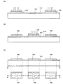
次に、ボンド基板100を部分的に除去する。本実施の形態では、図1(C)に示すように、マスク104を用い、絶縁膜101と共にボンド基板100を部分的にエッチングにより除去し、複数の凸部103を有するボンド基板100を形成する。
Next, the
ボンド基板100は、複数の凸部103のボンド基板100に対して垂直方向(深さ方向)における幅dが、欠陥層102の深さと同じか、それ以上の大きさを有する。なお、複数の凸部103のボンド基板100に対して垂直方向(深さ方向)における幅dは、必ずしも一定である必要はなく、場所によって異なる値を有していてもよい。具体的に、幅dは、半導体膜106の厚さを考慮して、例えば10nm以上、好ましくは200nm以上とする。
The
なお、ボンド基板100は、反りや撓みを有している場合や、端部に若干丸みを帯びている場合がある。そして、ボンド基板100から半導体膜を剥離するために水素または希ガス、あるいは水素イオンまたは希ガスイオンを照射する際、ボンド基板100の端部において上記ガスまたはイオンの添加を十分に行うことができない場合もある。そのため、ボンド基板100の端部に位置する部分は、半導体膜を剥離させるのが難しい。よって、ボンド基板100が有する複数の凸部103は、ボンド基板100の縁から所定の間隔を有するよう、離れた位置に形成するのが望ましい。ボンド基板100の縁から所定の間隔を有するよう、離れた位置に凸部103を形成することで、再現性よく分離または劈開による半導体膜の形成を行うことができる。例えば、最も端部に位置する凸部103と、ボンド基板100の縁との間隔は、数十μm乃至数十mmとするとよい。
Note that the
次に、マスク104を除去した後、熱処理を行うことにより、欠陥層102において隣接する微小ボイドどうしが結合して、微小ボイドの体積が増大する。その結果、欠陥層102においてボンド基板100が分離または劈開し、凸部103の一部であった半導体膜106が、絶縁膜101と共に、ボンド基板100から剥離する。熱処理は、例えば400℃乃至600℃の温度範囲内で行えばよい。
Next, after the
なお、熱処理は、マイクロ波などの高周波による誘電加熱を用いて行ってもよい。上記誘電加熱による熱処理は、高周波発生装置において生成された周波数300MHz乃至3THzの高周波をボンド基板100に照射することで行うことができる。具体的には、例えば、2.45GHzのマイクロ波を900W、14分間照射することで、欠陥層において隣接する微小ボイドどうしを結合させ、最終的にボンド基板100を分離または劈開させることができる。
Note that the heat treatment may be performed using dielectric heating by a high frequency such as a microwave. The heat treatment by the dielectric heating can be performed by irradiating the
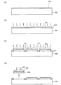
そして、図1(D)に示すように、コレット105を半導体膜106上に形成された絶縁膜101に固着させ、半導体膜106をボンド基板100から引き離す。上記熱処理によるボンド基板100の分離または劈開が不完全である場合でも、コレット105を用いて力を加えることで、半導体膜106をボンド基板100から完全に剥離させることができる。コレット105として、真空チャック、メカニカルチャックなどのチャック、先端に接着剤が付着したマイクロニードルなど、凸部103の1つに選択的に固着させることができる手段を用いる。図1(D)では、コレット105として真空チャックを用いる場合を例示している。
Then, as shown in FIG. 1D, the
また、マイクロニードルに付着させる接着剤として、エポキシ系接着剤、セラミック系接着剤、シリコーン系接着剤、低温凝固剤などを用いることができる。低温凝固剤は、例えばMW−1(株式会社エミネントサプライ製)を用いることができる。MW−1は、凝固点が17度付近であり、凝固点以下の温度(好ましくは、10度以下)で接着効果を有し、凝固点以上の温度(好ましくは25度程度)では接着効果を有さない。 In addition, as an adhesive to be attached to the microneedle, an epoxy adhesive, a ceramic adhesive, a silicone adhesive, a low-temperature coagulant, or the like can be used. For example, MW-1 (manufactured by Eminent Supply Co., Ltd.) can be used as the low temperature coagulant. MW-1 has a freezing point near 17 degrees, has an adhesive effect at a temperature below the freezing point (preferably 10 degrees or less), and has no adhesive effect at a temperature above the freezing point (preferably about 25 degrees). .
なお、ボンド基板100を分離または劈開させる前に、ボンド基板100に水素化処理を行うようにしてもよい。水素化処理は、例えば、水素雰囲気中において350℃、2時間程度行う。
Note that hydrogenation treatment may be performed on the
次に、図2(A)に示すように、半導体膜106の剥離により露出した面がベース基板107側を向くように、半導体膜106とベース基板107とを貼り合わせる。本実施の形態では、ベース基板107上に絶縁膜114が形成されており、絶縁膜114と半導体膜106とが接合することで、半導体膜106とベース基板107とを貼り合わせることができる。半導体膜106と絶縁膜114とを接合させた後、該接合をさらに強固にするため、400℃乃至600℃の熱処理を行うのが好ましい。
Next, as illustrated in FIG. 2A, the
接合の形成はファン・デル・ワールス力を用いて行われているため、室温でも強固な接合が形成される。なお、上記接合は低温で行うことが可能であるため、ベース基板107は様々なものを用いることが可能である。例えばベース基板107としては、アルミノシリケートガラス、バリウムホウケイ酸ガラス、アルミノホウケイ酸ガラスなどのガラス基板の他、石英基板、サファイア基板などの基板を用いることができる。さらにベース基板107として、シリコン、ガリウムヒ素、インジウムリンなどの半導体基板などを用いることができる。あるいは、ステンレス基板を含む金属基板をベース基板107として用いてもよい。
Since the bond is formed using van der Waals force, a strong bond is formed even at room temperature. Note that since the bonding can be performed at a low temperature, a variety of
なお、ベース基板107は、その表面に絶縁膜114が必ずしも形成されていなくともよい。絶縁膜114が形成されていない場合でも、ベース基板107と半導体膜106とを接合させることは可能である。ただし、ベース基板107の表面に絶縁膜114を形成しておくことで、ベース基板107から半導体膜106に、アルカリ金属やアルカリ土類金属などの不純物が入り込むのを防ぐことができる。
Note that the insulating
絶縁膜114を形成する場合、ベース基板107ではなく絶縁膜114が半導体膜106と接合するので、ベース基板107として用いることができる基板の種類がさらに広がる。プラスチック等の可撓性を有する合成樹脂からなる基板は耐熱温度が一般的に低い傾向にあるが、作製工程における処理温度に耐え得るのであれば、絶縁膜114を形成する場合において、ベース基板107として用いることが可能である。プラスチック基板として、ポリエチレンテレフタレート(PET)に代表されるポリエステル、ポリエーテルスルホン(PES)、ポリエチレンナフタレート(PEN)、ポリカーボネート(PC)、ポリエーテルエーテルケトン(PEEK)、ポリスルホン(PSF)、ポリエーテルイミド(PEI)、ポリアリレート(PAR)、ポリブチレンテレフタレート(PBT)、ポリイミド、アクリロニトリルブタジエンスチレン樹脂、ポリ塩化ビニル、ポリプロピレン、ポリ酢酸ビニル、アクリル樹脂などが挙げられる。
In the case where the insulating
なお、半導体膜106をベース基板107上に貼り合わせる前または貼り合わせた後に、半導体膜106の剥離により露出した面に、レーザ光の照射による熱アニールを施してもよい。半導体膜106をベース基板107上に貼り合わせる前に熱アニールを施すと、剥離により露出した面が平坦化され、接合の強度をより高めることができる。また、半導体膜106をベース基板107上に貼り合わせた後に熱アニールを施すと、半導体膜106が一部溶解し、接合の強度をより高めることができる。
Note that before or after the
レーザ光の照射による熱アニールを行う場合、半導体に選択的に吸収される固体レーザの基本波または第2高調波のレーザ光を照射することが望ましい。例えば、連続発振のYAGレーザから射出された出力100Wのレーザ光を用いる。そして、好ましくは光学系により照射面にて矩形状または楕円形状のレーザ光に成形して、半導体膜106の剥離により露出した面に照射する。このときのパワー密度は1kW/cm2〜100MW/cm2程度(好ましくは0.1〜10MW/cm2)が必要である。そして、走査速度を10〜2000cm/sec程度とし、照射する。
In the case of performing thermal annealing by laser light irradiation, it is desirable to irradiate a fundamental wave or second harmonic laser light of a solid-state laser that is selectively absorbed by a semiconductor. For example, laser light having an output of 100 W emitted from a continuous wave YAG laser is used. Then, it is preferably formed into a rectangular or elliptical laser beam on the irradiation surface by an optical system, and the surface exposed by peeling of the
レーザ光の照射による熱アニールには、連続発振の気体レーザであるArレーザ、Krレーザなどを用いることができる。また、連続発振の固体レーザであるYAGレーザ、YVO4レーザ、YLFレーザ、YAlO3レーザ、フォルステライト(Mg2SiO4)レーザ、GdVO4レーザ、Y2O3レーザ、ガラスレーザ、ルビーレーザ、アレキサンドライトレーザ、Ti:サファイアレーザなどを用いることができる。また、パルス発振のレーザである、Arレーザ、Krレーザ、エキシマレーザ、CO2レーザ、YAGレーザ、Y2O3レーザ、YVO4レーザ、YLFレーザ、YAlO3レーザ、ガラスレーザ、ルビーレーザ、アレキサンドライトレーザ、Ti:サファイアレーザ、銅蒸気レーザまたは金蒸気レーザなどを用いることができる。 For thermal annealing by laser light irradiation, an Ar laser, a Kr laser, or the like that is a continuous wave gas laser can be used. Further, a continuous wave solid-state laser, YAG laser, YVO 4 laser, YLF laser, YAlO 3 laser, forsterite (Mg 2 SiO 4 ) laser, GdVO 4 laser, Y 2 O 3 laser, glass laser, ruby laser, alexandrite A laser, a Ti: sapphire laser, or the like can be used. Further, Ar laser, Kr laser, excimer laser, CO 2 laser, YAG laser, Y 2 O 3 laser, YVO 4 laser, YLF laser, YAlO 3 laser, glass laser, ruby laser, and alexandrite laser are pulse oscillation lasers. Ti: sapphire laser, copper vapor laser, gold vapor laser, or the like can be used.
また、半導体膜106をベース基板107上に接合のみによって貼り合わせるのではなく、半導体膜106に10MHz〜1THz程度の高周波数の振動を加えることで、半導体膜106とベース基板107の間に摩擦熱を生じさせ、該熱により半導体膜106を部分的に溶解させ、半導体膜106をベース基板107上に貼り合わせるようにしてもよい。
In addition, the
なお、MW−1を低温凝固剤として用いる場合、まず低温凝固剤が接着効果を有しない温度(例えば25度程度)において、マイクロニードルの先端に付着した低温凝固剤を、凸部103上の絶縁膜101に接触させる。次に、低温凝固剤が接着効果を有する温度(例えば5度程度)まで温度を下げて、低温凝固剤を凝固させることで、マイクロニードルと凸部103上の絶縁膜101とを固着させる。そして、ボンド基板100から引き離した半導体膜106を、ベース基板107上に貼り合わせた後、再び接着効果を有しない温度(例えば25度程度)まで低温凝固剤の温度を高めることで、マイクロニードルを半導体膜106から引き離すことができる。
When MW-1 is used as a low-temperature coagulant, first, the low-temperature coagulant adhering to the tip of the microneedle is insulated on the
次に図2(B)に示すように、半導体膜106を形成するボンド基板100とは異なる結晶面方位を有するボンド基板から、半導体膜106と同様の手法を用いて半導体膜108を剥離し、ベース基板107上に貼り合わせる。
Next, as illustrated in FIG. 2B, the
半導体中における多数キャリアの移動度は、結晶面方位によって異なる。よって、形成する半導体素子に適した結晶面方位を有するボンド基板を、適宜選択して半導体膜106または半導体膜108を形成すればよい。例えば半導体膜106を用いてn型の半導体素子を形成するならば、{100}面を有する半導体膜106を形成することで、該半導体素子における多数キャリアの移動度を高めることができる。また、例えば半導体膜108を用いてp型の半導体素子を形成するならば、{110}面を有する半導体膜108を形成することで、該半導体素子における多数キャリアの移動度を高めることができる。そして、半導体素子としてトランジスタを形成するならば、チャネルの向きと結晶面方位とを考慮し、半導体膜106または半導体膜108の貼り合わせの方向を定めるようにする。
The mobility of majority carriers in a semiconductor varies depending on the crystal plane orientation. Therefore, the
なお、上述したように、ボンド基板は、反りや撓みを有している場合や、端部に若干丸みを帯びている場合がある。また、ボンド基板から半導体膜を剥離するために水素または希ガス、あるいは水素イオンまたは希ガスイオンを照射する際、ボンド基板の端部において上記ガスまたはイオンの添加を十分に行うことができない場合もある。そのため、ボンド基板の端部に位置する部分は、半導体膜を剥離させるのが難しく、ボンド基板をベース基板に貼り合わせた後にボンド基板を分離または劈開して半導体膜を形成する場合、半導体膜間の間隔が数mm〜数cmとなってしまう。しかし、本発明では、ボンド基板をベース基板107に貼り合わせる前に、ボンド基板を分離または劈開させて半導体膜106と半導体膜108を形成している。よって、半導体膜106と半導体膜108をベース基板107上に貼り合わせる際、半導体膜106と半導体膜108の間隔を、数十μm程度に小さく抑えることができ、半導体膜106と半導体膜108の隙間をまたぐように半導体装置を作製することが容易となる。
Note that, as described above, the bond substrate may be warped or bent, or the end may be slightly rounded. In addition, when irradiation with hydrogen or a rare gas, or hydrogen ions or rare gas ions in order to peel the semiconductor film from the bond substrate, the gas or ions may not be sufficiently added at the edge of the bond substrate. is there. Therefore, it is difficult to peel off the semiconductor film at the portion located at the edge of the bond substrate. When the semiconductor substrate is formed by separating or cleaving the bond substrate after bonding the bond substrate to the base substrate, Will be several mm to several cm. However, in the present invention, the
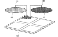
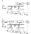
図4に、結晶面方位が互いに異なるボンド基板160とボンド基板161から、それぞれ半導体膜163と半導体膜164を剥離し、該半導体膜163と半導体膜164をベース基板162上に貼り合わせている様子を示す。ベース基板162上において半導体膜163と半導体膜164を貼り合わせる位置は、半導体素子のマスク図面の情報を元に決めることができる。なお、図4では2つのボンド基板160、ボンド基板161から半導体膜163と半導体膜164を剥離する例について示しているが、ボンド基板は3つ以上用いていてもよい。
4A and 4B, the
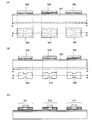
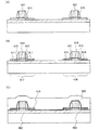
次に図2(C)に示すように、半導体膜106および半導体膜108上に形成されている絶縁膜101を除去する。図2(C)には、半導体膜106および半導体膜108の断面図に加えて、半導体膜106および半導体膜108の上面図も示す。図2(C)に示す断面図は、上面図の破線A−A’における断面に相当する。
Next, as illustrated in FIG. 2C, the
次に、図3(A)に示すように、半導体膜106と半導体膜108を部分的にエッチングすることで、半導体膜106から半導体膜109を、半導体膜108から半導体膜110を形成する。図3(A)には、半導体膜109および半導体膜110の断面図に加えて、半導体膜109および半導体膜110の上面図も示す。図3(A)に示す断面図は、上面図の破線A−A’における断面に相当する。半導体膜106および半導体膜108をさらにエッチングすることで、半導体膜106および半導体膜108の端部において接合の強度が不十分である領域を、除去することができる。
Next, as illustrated in FIG. 3A, the
なお、本実施の形態では、1つの半導体膜106をエッチングすることで1つの半導体膜109を形成し、1つの半導体膜108をエッチングすることで1つの半導体膜110を形成しているが、本発明はこの構成に限定されない。例えば、1つの半導体膜106をエッチングすることで複数の半導体膜109を形成してもよいし、1つの半導体膜108をエッチングすることで複数の半導体膜110を形成してもよい。
Note that in this embodiment, one
図3(A)に示すように半導体膜109および半導体膜110が形成された後、半導体膜109および半導体膜110の表面を平坦化してもよい。平坦化は必ずしも必須ではないが、平坦化を行うことで、後に形成されるトランジスタにおいて半導体膜109および半導体膜110とゲート絶縁膜の界面の特性を向上させることができる。具体的に平坦化は、化学的機械的研磨(CMP:Chemical Mechanical Polishing)または液体ジェット研磨などにより、行うことができる。半導体膜109および半導体膜110の厚さは、上記平坦化により薄膜化される。上記平坦化は、エッチングにより形成された半導体膜109および半導体膜110に施してもよいし、エッチングする前の半導体膜106および半導体膜108に施してもよい。
After the
なお、分離または劈開により露出される半導体膜の表面と、ゲート絶縁膜とが接するように、半導体膜をベース基板上に貼り合わせることもできる。ただし、本実施の形態のように、分離または劈開により露出される半導体膜の表面をベース基板側に向けると、より平坦性の高い側の表面がゲート絶縁膜に接するため、半導体膜とゲート絶縁膜の間の界面準位密度を低く、なおかつ均一にすることができる。よって、ゲート絶縁膜に接する半導体膜の表面を平坦化するための研磨を省略、もしくは研磨時間を短縮化することができ、コストを抑えスループットを向上させることができる。 Note that the semiconductor film can be attached to the base substrate so that the surface of the semiconductor film exposed by separation or cleavage is in contact with the gate insulating film. However, as in this embodiment, when the surface of the semiconductor film exposed by separation or cleavage is directed to the base substrate side, the surface with higher flatness is in contact with the gate insulating film; The interface state density between the films can be made low and uniform. Accordingly, polishing for planarizing the surface of the semiconductor film in contact with the gate insulating film can be omitted or the polishing time can be shortened, and cost can be reduced and throughput can be improved.
また、半導体膜109および半導体膜110、あるいはエッチングを行う前の半導体膜106および半導体膜108にエネルギービームを照射して、結晶欠陥を補修してもよい。エネルギービームは、半導体に選択的に吸収されるもの、例えばレーザ光を用いるのが望ましい。レーザ光は、エキシマレーザなどの気体レーザ、YAGレーザなどの固体レーザを光源として用いることができる。レーザ光の波長は、紫外光から近赤外光であることが好ましく、波長190nm〜2000nmの領域のレーザ光を用いるのが望ましい。その他、ハロゲンランプ若しくはキセノンランプなどを用いたフラッシュランプアニールを、結晶欠陥の補修のために用いてもよい。
Alternatively, the
なお本実施の形態では、欠陥層102の形成により半導体膜106と半導体膜108とを、ボンド基板100からそれぞれ剥離するスマートカット法を用いる場合について示すが、ELTRAN(Epitaxial Layer Transfer)、誘電体分離法、PACE(Plasma Assisted Chemical Etching)法などの、他の貼り合わせ法を用いてもよい。
Note that in this embodiment mode, a smart cut method in which the
上記工程を経て形成された半導体膜109、半導体膜110を用い、図3(B)に示すようにトランジスタ111〜113などの各種半導体素子を形成することができる。
Various semiconductor elements such as the
本実施の形態の半導体装置の作製方法では、複数のボンド基板100を用いて1つのベース基板に複数の半導体膜を貼り合わせるので、大型のベース基板107に対しても高スループットで処理を行うことができる。また、半導体素子の有する極性に合わせて半導体膜の面方位を適宜選択することができるので、半導体素子の移動度を高めることができ、より高速駆動が可能な半導体装置を提供することができる。
In the method for manufacturing a semiconductor device of this embodiment mode, a plurality of semiconductor films are attached to one base substrate using a plurality of
また、本発明の半導体装置の作製方法の1つでは、ボンド基板100を複数箇所において分離または劈開することで複数の半導体膜106を形成し、該複数の半導体膜をベース基板上に貼り合わせることができるので、半導体装置における半導体素子の極性およびレイアウトに合わせて、複数の各半導体膜106を貼り合わせる位置を選択することができる。
In one method for manufacturing a semiconductor device of the present invention, a plurality of
なお本発明は、マイクロプロセッサ、画像処理回路などの集積回路や、質問器とデータの送受信が非接触でできるRFタグ、半導体表示装置等、ありとあらゆる半導体装置の作製に用いることができる。半導体表示装置には、液晶表示装置、有機発光素子(OLED)に代表される発光素子を各画素に備えた発光装置、DMD(Digital Micromirror Device)、PDP(Plasma Display Panel)、FED(Field Emission Display)等や、半導体膜を用いた回路素子を駆動回路に有しているその他の半導体表示装置がその範疇に含まれる。 Note that the present invention can be used for manufacturing various kinds of semiconductor devices such as an integrated circuit such as a microprocessor and an image processing circuit, an RF tag capable of transmitting and receiving data to and from an interrogator, and a semiconductor display device. The semiconductor display device includes a liquid crystal display device, a light-emitting device including a light-emitting element typified by an organic light-emitting element (OLED) in each pixel, DMD (Digital Micromirror Device), PDP (Plasma Display Panel), FED (Field Emission Display). ) And other semiconductor display devices having a circuit element using a semiconductor film in a drive circuit are included in the category.
(実施の形態2)
本実施の形態では、実施の形態1に示した作製方法において、エッチングによりボンド基板に凸部を形成する代わりに、ドーピングを用いてボンド基板に欠陥層を形成する、本発明の半導体装置の作製方法の1つについて説明する。
(Embodiment 2)
In this embodiment mode, in the manufacturing method described in
まず図5(A)に示すように、ボンド基板200上に絶縁膜201を形成する。ボンド基板200として、シリコン、ゲルマニウムなどの単結晶半導体基板または多結晶半導体基板を用いることができる。その他に、ガリウムヒ素、インジウムリンなどの化合物半導体で形成された単結晶半導体基板または多結晶半導体基板を、ボンド基板200として用いることができる。またボンド基板200として、結晶格子に歪みを有するシリコン、シリコンに対しゲルマニウムが添加されたシリコンゲルマニウムなどの半導体基板を用いていてもよい。歪みを有するシリコンは、シリコンよりも格子定数の大きいシリコンゲルマニウムまたは窒化珪素上における成膜により、形成することができる。
First, as illustrated in FIG. 5A, the insulating
絶縁膜201は、酸化珪素、窒化酸化珪素、酸化窒化珪素、窒化珪素等の絶縁性を有する材料を用いて形成する。絶縁膜201は、単数の絶縁膜を用いたものであっても、複数の絶縁膜を積層して用いたものであってもよい。例えば本実施の形態では、酸化珪素を絶縁膜201として用いる。
The insulating
酸化珪素を絶縁膜201として用いる場合、絶縁膜201はシランと酸素、TEOS(テトラエトキシシラン)と酸素等の混合ガスを用い、熱CVD、プラズマCVD、常圧CVD、バイアスECRCVD等の気相成長法によって形成することができる。この場合、絶縁膜201の表面を酸素プラズマ処理で緻密化してもよい。また、窒化珪素を絶縁膜201として用いる場合、シランとアンモニアの混合ガスを用い、プラズマCVD等の気相成長法によって形成することができる。また、窒化酸化珪素を絶縁膜201として用いる場合、シランとアンモニアの混合ガス、またはシランと酸化窒素の混合ガスを用い、プラズマCVD等の気相成長法によって形成することができる。
When silicon oxide is used as the insulating
また、有機シランガスを用いて化学気相成長法により作製される酸化珪素を、絶縁膜201として用いてもよい。有機シランガスとしては、テトラエトキシシラン(TEOS:化学式Si(OC2H5)4)、テトラメチルシラン(TMS:化学式Si(CH3)4)、テトラメチルシクロテトラシロキサン(TMCTS)、オクタメチルシクロテトラシロキサン(OMCTS)、ヘキサメチルジシラザン(HMDS)、トリエトキシシラン(SiH(OC2H5)3)、トリスジメチルアミノシラン(SiH(N(CH3)2)3)等のシリコン含有化合物を用いることができる。
Alternatively, silicon oxide formed by a chemical vapor deposition method using an organosilane gas may be used as the insulating
次に図5(B)に示すように、ボンド基板200に、矢印で示すように水素または希ガス、あるいは水素イオンまたは希ガスイオンを照射し、ボンド基板200の表面から一定の深さの領域に、微小ボイドを有する欠陥層202を形成する。欠陥層202が形成される位置は、上記照射の加速電圧によって決まる。そして欠陥層202の位置により、ボンド基板200から形成される半導体膜206の厚さが決まるので、照射の加速電圧は上記半導体膜206の厚さを考慮して行う。また上記照射の加速電圧のみならず、絶縁膜201の膜厚によっても、欠陥層202の位置を変えることができる。例えば、絶縁膜201の膜厚をより大きくすることで、半導体膜206の膜厚をより小さくすることができる。半導体膜206の厚さは、例えば10nm乃至200nm、好ましくは10nm乃至50nmの厚さとする。例えば水素をボンド基板200に照射する場合、ドーズ量は1×10¹⁶乃至1×10¹⁷/cm2とするのが望ましい。本実施の形態では、ドーズ量を1.75×1016/cm2、加速電圧を40kVとし、水素または水素イオンの照射を行う。
Next, as illustrated in FIG. 5B, the
なお、欠陥層202を形成する上記工程において、ボンド基板200に高い濃度の水素または希ガス、あるいは水素イオンまたは希ガスイオンを照射するので、ボンド基板200の表面が粗くなってしまい、ボンド基板200から形成される半導体膜と、該半導体膜に接するゲート絶縁膜との界面準位密度にばらつきが生じてしまう場合がある。絶縁膜201を設けることで、水素または希ガス、あるいは水素と希ガスのイオンを照射する際にボンド基板200の表面が保護され、ボンド基板200の表面が荒れるのを防ぎ、上記界面準位密度にばらつきが生じるのを防ぐことができる。
Note that in the above step of forming the
また、ボンド基板200にレーザ光を照射し、ボンド基板200に多光子吸収を起こすことで、欠陥層202を形成してもよい。この方法を用いると、ボンド基板200にダメージを与えることなく、半導体膜をボンド基板200から剥離することができる。
Alternatively, the
次に、絶縁膜201上にマスク210を形成し、矢印で示すように水素または希ガス、あるいは水素イオンまたは希ガスイオンをボンド基板200に選択的に添加し、微小ボイドを有する欠陥層211を形成する。欠陥層211を形成する場合、欠陥層202を形成する場合よりも、照射するガスまたはイオンのドーズ量を多くするか、もしくはより大きい質量を有するガスまたはイオンを照射する。上記構成により、ボンド基板200の深さ方向における欠陥層211の幅を広くすることができる。例えば水素をボンド基板200に照射する場合、ドーズ量は5×10¹⁷乃至5×10¹⁸/cm2とするのが望ましい。本実施の形態では、ドーズ量を1×1018/cm2、加速電圧を40kVとし、水素または水素イオンの照射を行う。
Next, a mask 210 is formed over the insulating
また、ボンド基板200にレーザ光を照射し、ボンド基板200に多光子吸収を起こすことで、欠陥層211を形成してもよい。
Alternatively, the
欠陥層211のボンド基板200に対して垂直方向(深さ方向)における幅dは、欠陥層202の深さと同じか、それ以上の大きさを有することが望ましい。具体的に、幅dは、半導体膜206の厚さを考慮して、例えば10nm以上、好ましくは200nm以上とする。
It is desirable that the width d of the
なお、ボンド基板200は、反りや撓みを有している場合や、端部に若干丸みを帯びている場合がある。そして、ボンド基板200から半導体膜を剥離するためにガスまたはイオンを照射する際、ボンド基板200の端部においてイオン等の添加を十分に行うことができない場合もある。そのため、ボンド基板200の端部に位置する部分は、半導体膜を剥離させるのが難しい。よって、欠陥層211を、ボンド基板200の端部においても形成することが望ましい。ボンド基板200の端部に欠陥層211を形成することで、端部の分離または劈開しにくい箇所を避けて、再現性よく分離または劈開による半導体膜の形成を行うことができる。例えば、端部に位置する欠陥層211の、幅dに対して垂直方向における幅は、数十μm乃至数十mmとするとよい。
Note that the
次に、マスク210を除去した後に熱処理を行うことにより、欠陥層202および欠陥層211において隣接する微小ボイドどうしが結合して、微小ボイドの体積が増大する。その結果、欠陥層202および欠陥層211においてボンド基板200が分離または劈開し、半導体膜206が絶縁膜201と共に、ボンド基板200から剥離する。熱処理は、例えば400℃乃至600℃の温度範囲内で行えばよい。
Next, heat treatment is performed after the mask 210 is removed, whereby adjacent microvoids in the
なお、熱処理は、マイクロ波などの高周波による誘電加熱を用いて行ってもよい。上記誘電加熱による熱処理は、高周波発生装置において生成された周波数300MHz乃至3THzの高周波をボンド基板200に照射することで行うことができる。具体的には、例えば、2.45GHzのマイクロ波を900W、14分間照射することで、欠陥層において隣接する微小ボイドどうしを結合させ、最終的にボンド基板200を分離または劈開させることができる。
Note that the heat treatment may be performed using dielectric heating by a high frequency such as a microwave. The heat treatment by the dielectric heating can be performed by irradiating the
そして、図5(D)に示すように、コレット205を半導体膜206上に形成された絶縁膜201に固着させ、半導体膜206をボンド基板200から引き離す。上記熱処理によるボンド基板200の分離または劈開が不完全である場合でも、コレット205を用いて力を加えることで、半導体膜206をボンド基板200から完全に剥離させることができる。コレット205として、真空チャック、メカニカルチャックなどのチャック、先端に接着剤が付着したマイクロニードルなど、半導体膜206の1つに選択的に固着させることができる手段を用いる。図5(D)では、コレット205として真空チャックを用いる場合を例示している。
Then, as shown in FIG. 5D, the
なお、ボンド基板200を分離または劈開させる前に、ボンド基板200に水素化処理を行うようにしてもよい。水素化処理は、例えば、水素雰囲気中において350℃、2時間程度行う。
Note that the
また、マイクロニードルに付着させる接着剤として、エポキシ系接着剤、セラミック系接着剤、シリコーン系接着剤、低温凝固剤などを用いることができる。低温凝固剤は、例えばMW−1(株式会社エミネントサプライ製)を用いることができる。 In addition, as an adhesive to be attached to the microneedle, an epoxy adhesive, a ceramic adhesive, a silicone adhesive, a low-temperature coagulant, or the like can be used. For example, MW-1 (manufactured by Eminent Supply Co., Ltd.) can be used as the low temperature coagulant.
以下、実施の形態1と同様の作製方法を経て、本発明の半導体装置を作製することができる。
Hereinafter, the semiconductor device of the present invention can be manufactured through a manufacturing method similar to that of
(実施の形態3)
本実施の形態では、本発明の半導体装置の作製方法の1つについて説明する。
(Embodiment 3)
In this embodiment, one method for manufacturing a semiconductor device of the present invention will be described.
まず図6(A)に示すように、ボンド基板300上に絶縁膜301を形成する。ボンド基板300として、シリコン、ゲルマニウムなどの単結晶半導体基板または多結晶半導体基板を用いることができる。その他に、ガリウムヒ素、インジウムリンなどの化合物半導体で形成された単結晶半導体基板または多結晶半導体基板を、ボンド基板300として用いることができる。またボンド基板300として、結晶格子に歪みを有するシリコン、シリコンに対しゲルマニウムが添加されたシリコンゲルマニウムなどの半導体基板を用いていてもよい。歪みを有するシリコンは、シリコンよりも格子定数の大きいシリコンゲルマニウムまたは窒化珪素上における成膜により、形成することができる。
First, as illustrated in FIG. 6A, an insulating
絶縁膜301は、酸化珪素、窒化酸化珪素、酸化窒化珪素、窒化珪素等の絶縁性を有する材料を用いて形成する。絶縁膜301は、単数の絶縁膜を用いたものであっても、複数の絶縁膜を積層して用いたものであってもよい。例えば本実施の形態では、ボンド基板300に近い側から、窒素よりも酸素の含有量が高い酸化窒化珪素、酸素よりも窒素の含有量が高い窒化酸化珪素の順に積層された絶縁膜301を用いる。
The insulating
酸化珪素を絶縁膜301として用いる場合、絶縁膜301はシランと酸素、TEOS(テトラエトキシシラン)と酸素等の混合ガスを用い、熱CVD、プラズマCVD、常圧CVD、バイアスECRCVD等の気相成長法によって形成することができる。この場合、絶縁膜301の表面を酸素プラズマ処理で緻密化してもよい。また、窒化珪素を絶縁膜301として用いる場合、シランとアンモニアの混合ガスを用い、プラズマCVD等の気相成長法によって形成することができる。また、窒化酸化珪素を絶縁膜301として用いる場合、シランとアンモニアの混合ガス、またはシランと酸化窒素の混合ガスを用い、プラズマCVD等の気相成長法によって形成することができる。
When silicon oxide is used as the insulating
また、有機シランガスを用いて化学気相成長法により作製される酸化珪素を、絶縁膜301として用いてもよい。有機シランガスとしては、テトラエトキシシラン(TEOS:化学式Si(OC2H5)4)、テトラメチルシラン(TMS:化学式Si(CH3)4)、テトラメチルシクロテトラシロキサン(TMCTS)、オクタメチルシクロテトラシロキサン(OMCTS)、ヘキサメチルジシラザン(HMDS)、トリエトキシシラン(SiH(OC2H5)3)、トリスジメチルアミノシラン(SiH(N(CH3)2)3)等のシリコン含有化合物を用いることができる。
Alternatively, silicon oxide formed by a chemical vapor deposition method using an organosilane gas may be used for the insulating
次に、ボンド基板300に、矢印で示すように水素または希ガス、あるいは水素イオンまたは希ガスイオンを照射し、ボンド基板300の表面から一定の深さの領域に、微小ボイドを有する欠陥層302を形成する。欠陥層302が形成される位置は、上記照射の加速電圧によって決まる。そして欠陥層302の位置により、ボンド基板300から形成される半導体膜306、半導体膜308の厚さが決まるので、照射の加速電圧は上記半導体膜306、半導体膜308の厚さを考慮して行う。また上記照射の加速電圧のみならず、絶縁膜301の膜厚によっても、欠陥層302の位置を変えることができる。例えば、絶縁膜301の膜厚をより大きくすることで、半導体膜306、半導体膜308の膜厚をより小さくすることができる。半導体膜306、半導体膜308の厚さは、例えば10nm乃至200nm、好ましくは10nm乃至50nmの厚さとする。例えば水素をボンド基板300に照射する場合、ドーズ量は1×10¹⁶乃至1×10¹⁷/cm2とするのが望ましい。本実施の形態では、ドーズ量を1.75×1016/cm2、加速電圧を40kVとし、水素または水素イオンの照射を行う。
Next, the
なお、欠陥層302を形成する上記工程において、ボンド基板300に高い濃度の水素または希ガス、あるいは水素イオンまたは希ガスイオンを照射するので、ボンド基板300の表面が粗くなってしまい、ベース基板307との間における接合で十分な強度が得られない場合がある。絶縁膜301を設けることで、水素または希ガス、あるいは水素と希ガスのイオンを照射する際にボンド基板300の表面が保護され、半導体膜306、半導体膜308とベース基板307の間における接合を良好に行うことができる。
Note that in the above step of forming the
また、ボンド基板300にレーザ光を照射し、ボンド基板300に多光子吸収を起こすことで、欠陥層302を形成してもよい。この方法を用いると、ボンド基板300にダメージを与えることなく、半導体膜をボンド基板300から剥離することができる。
Alternatively, the
次に図6(B)に示すように、絶縁膜301上に絶縁膜320を形成する。絶縁膜320は、絶縁膜301と同様に、酸化珪素、窒化酸化珪素、酸化窒化珪素、窒化珪素等の絶縁性を有する材料を用いて形成する。絶縁膜320は、単数の絶縁膜を用いたものであっても、複数の絶縁膜を積層して用いたものであってもよい。また、有機シランガスを用いて化学気相成長法により作製される酸化珪素を、絶縁膜320として用いてもよい。本実施の形態では、有機シランガスを用いて化学気相成長法により作製される酸化珪素を、絶縁膜320として用いる。
Next, as illustrated in FIG. 6B, the insulating
なお絶縁膜301または絶縁膜320に窒化珪素、窒化酸化珪素などのバリア性の高い絶縁膜を用いることで、アルカリ金属やアルカリ土類金属などの不純物が、ベース基板307から、ベース基板307上に形成される半導体膜306および半導体膜308に入るのを防ぐことができる。
Note that by using an insulating film with a high barrier property such as silicon nitride or silicon nitride oxide for the insulating
なお本実施の形態では、欠陥層302を形成した後に絶縁膜320を形成しているが、絶縁膜320は必ずしも設ける必要はない。ただし絶縁膜320は欠陥層302を形成した後に形成されるので、欠陥層302を形成する前に形成される絶縁膜301よりも、その表面の平坦性は高い。よって、絶縁膜320を形成することで、後に行われる接合の強度をより高めることができる。
Note that in this embodiment, the insulating
次に、ボンド基板300を部分的に除去する。本実施の形態では、図6(C)に示すように、マスク304を用い、絶縁膜301と共にボンド基板300を部分的にエッチングにより除去し、複数の凸部303を有するボンド基板300を形成する。
Next, the
ボンド基板300は、複数の凸部303のボンド基板300に対して垂直方向(深さ方向)における幅dが、欠陥層302の深さと同じか、それ以上の大きさを有する。なお、複数の凸部303のボンド基板300に対して垂直方向(深さ方向)における幅dは、必ずしも一定である必要はなく、場所によって異なる値を有していてもよい。具体的に、幅dは、半導体膜306の厚さを考慮して、例えば10nm以上、好ましくは200nm以上とする。
The
なお、ボンド基板300は、反りや撓みを有している場合や、端部に若干丸みを帯びている場合がある。そして、ボンド基板300から半導体膜を剥離するために水素または希ガス、あるいは水素イオンまたは希ガスイオンを照射する際、ボンド基板300の端部において上記ガスまたはイオンの添加を十分に行うことができない場合もある。そのため、ボンド基板300の端部に位置する部分は、半導体膜を剥離させるのが難しい。よって、ボンド基板300が有する複数の凸部303は、ボンド基板300の縁から所定の間隔を有するよう、離れた位置に形成するのが望ましい。ボンド基板300の縁から所定の間隔を有するよう、離れた位置に凸部303を形成することで、再現性よく分離または劈開による半導体膜の形成を行うことができる。例えば、最も端部に位置する凸部303と、ボンド基板300の縁との間隔は、数十μm乃至数十mmとするとよい。
Note that the
次に、マスク304を除去した後、ボンド基板300を保持手段321に固着させる。ボンド基板300の固着は、凸部303が保持手段321側を向くように行う。保持手段321として、後の熱処理に耐えることができ、なおかつ複数の凸部303と重なるように固着させることができる大型の真空チャックまたはメカニカルチャック、具体的には多孔質真空チャック、非接触式真空チャックなどを用いることができる。本実施の形態では、真空チャックを保持手段321として用いる例を示す。
Next, after removing the
次に、熱処理を行うことにより、欠陥層302において隣接する微小ボイドどうしが結合して、微小ボイドの体積が増大する。その結果、図7(A)に示すように、欠陥層302においてボンド基板300が分離または劈開し、凸部303の一部であった半導体膜306が、絶縁膜301、絶縁膜320と共に、ボンド基板300から剥離する。熱処理は、例えば400℃乃至600℃の温度範囲内で行えばよい。
Next, by performing heat treatment, adjacent microvoids in the
なお、熱処理は、マイクロ波などの高周波による誘電加熱を用いて行ってもよい。上記誘電加熱による熱処理は、高周波発生装置において生成された周波数300MHz乃至3THzの高周波をボンド基板300に照射することで行うことができる。具体的には、例えば、2.45GHzのマイクロ波を900W、14分間照射することで、欠陥層において隣接する微小ボイドどうしを結合させ、最終的にボンド基板300を分離または劈開させることができる。
Note that the heat treatment may be performed using dielectric heating by a high frequency such as a microwave. The heat treatment by dielectric heating can be performed by irradiating the
また、ボンド基板300を分離または劈開させる前に、ボンド基板300に水素化処理を行うようにしてもよい。水素化処理は、例えば、水素雰囲気中において350℃、2時間程度行う。
Alternatively, the
そして、図7(B)に示すように、コレット305を半導体膜306の分離または劈開により露出した面に固着させ、半導体膜306を保持手段321から引き離す。コレット305として、真空チャック、メカニカルチャックなどのチャック、先端に接着剤が付着したマイクロニードルなど、凸部303の1つに選択的に固着させることができる手段を用いる。図7(B)では、コレット305として真空チャックを用いる場合を例示している。
Then, as shown in FIG. 7B, the
なお、本実施の形態では、コレット305が半導体膜306の分離または劈開により露出した面に固着している例を示しているがコレット305により傷つくのを防ぐために、絶縁膜などの保護膜を形成してもよい。ただし、上記保護膜は、後にベース基板307に半導体膜306を貼り合わせた後に、除去する。
Note that although an example in which the
また、マイクロニードルに付着させる接着剤として、エポキシ系接着剤、セラミック系接着剤、シリコーン系接着剤、低温凝固剤などを用いることができる。低温凝固剤は、例えばMW−1(株式会社エミネントサプライ製)を用いることができる。MW−1は、凝固点が17度付近であり、凝固点以下の温度(好ましくは、10度以下)で接着効果を有し、凝固点以上の温度(好ましくは25度程度)では接着効果を有さない。 In addition, as an adhesive to be attached to the microneedle, an epoxy adhesive, a ceramic adhesive, a silicone adhesive, a low-temperature coagulant, or the like can be used. For example, MW-1 (manufactured by Eminent Supply Co., Ltd.) can be used as the low temperature coagulant. MW-1 has a freezing point near 17 degrees, has an adhesive effect at a temperature below the freezing point (preferably 10 degrees or less), and has no adhesive effect at a temperature above the freezing point (preferably about 25 degrees). .
次に、図7(C)に示すように、絶縁膜320がベース基板307側を向くように、すなわち分離または劈開により露出した面の反対側の面がベース基板307側を向くように、半導体膜306とベース基板307とを貼り合わせる。本実施の形態では、ベース基板307上に絶縁膜314が形成されており、絶縁膜314と絶縁膜320とが接合することで、半導体膜306とベース基板307とを貼り合わせることができる。絶縁膜314と絶縁膜320とを接合させた後、該接合をさらに強固にするため、400℃乃至600℃の熱処理を行うのが好ましい。
Next, as illustrated in FIG. 7C, the semiconductor film is formed so that the insulating
接合の形成はファン・デル・ワールス力を用いて行われているため、室温でも強固な接合が形成される。なお、上記接合は低温で行うことが可能であるため、ベース基板307は様々なものを用いることが可能である。例えばベース基板307としては、アルミノシリケートガラス、バリウムホウケイ酸ガラス、アルミノホウケイ酸ガラスなどのガラス基板の他、石英基板、サファイア基板などの基板を用いることができる。さらにベース基板307として、シリコン、ガリウムヒ素、インジウムリンなどの半導体基板などを用いることができる。あるいは、ステンレス基板を含む金属基板をベース基板307として用いてもよい。
Since the bond is formed using van der Waals force, a strong bond is formed even at room temperature. Note that since the bonding can be performed at a low temperature,
なお、ベース基板307は、その表面に絶縁膜314が必ずしも形成されていなくともよい。絶縁膜314が形成されていない場合でも、ベース基板307と絶縁膜320とを接合させることは可能である。ただし、ベース基板307の表面に絶縁膜314を形成しておくことで、ベース基板307から半導体膜306に、アルカリ金属やアルカリ土類金属などの不純物が入り込むのを防ぐことができる。
Note that the insulating
絶縁膜314を形成する場合、ベース基板307ではなく絶縁膜314が絶縁膜320と接合するので、ベース基板307として用いることができる基板の種類がさらに広がる。プラスチック等の可撓性を有する合成樹脂からなる基板は耐熱温度が一般的に低い傾向にあるが、作製工程における処理温度に耐え得るのであれば、絶縁膜314を形成する場合において、ベース基板307として用いることが可能である。プラスチック基板として、ポリエチレンテレフタレート(PET)に代表されるポリエステル、ポリエーテルスルホン(PES)、ポリエチレンナフタレート(PEN)、ポリカーボネート(PC)、ポリエーテルエーテルケトン(PEEK)、ポリスルホン(PSF)、ポリエーテルイミド(PEI)、ポリアリレート(PAR)、ポリブチレンテレフタレート(PBT)、ポリイミド、アクリロニトリルブタジエンスチレン樹脂、ポリ塩化ビニル、ポリプロピレン、ポリ酢酸ビニル、アクリル樹脂などが挙げられる。
In the case where the insulating
なお、半導体膜306をベース基板307上に貼り合わせる前に、絶縁膜320の表面を研磨してもよい。保持手段321が絶縁膜320に接触することで絶縁膜320の表面に傷が付いた場合でも、研磨によりその表面の平坦性を高めることができるので、接合の強度を確保することができる。
Note that the surface of the insulating
なお、MW−1を低温凝固剤として用いる場合、まず低温凝固剤が接着効果を有しない温度(例えば25度程度)において、マイクロニードルの先端に付着した低温凝固剤を、凸部303上の絶縁膜320に接触させる。次に、低温凝固剤が接着効果を有する温度(例えば5度程度)まで温度を下げて、低温凝固剤を凝固させることで、マイクロニードルと凸部303上の絶縁膜320とを固着させる。そして、保持手段321から引き離した半導体膜306を、ベース基板307上に貼り合わせた後、再び接着効果を有しない温度(例えば25度程度)まで低温凝固剤の温度を高めることで、マイクロニードルを半導体膜306から引き離すことができる。
When MW-1 is used as a low-temperature coagulant, first, the low-temperature coagulant adhering to the tip of the microneedle is insulated on the
また図7(C)では、半導体膜306を形成するボンド基板300とは異なる結晶面方位を有するボンド基板から、半導体膜306と同様の手法を用いて半導体膜308を剥離し、ベース基板307上に貼り合わせる。
In FIG. 7C, the
半導体中における多数キャリアの移動度は、結晶面方位によって異なる。よって、形成する半導体素子に適した結晶面方位を有するボンド基板を、適宜選択して半導体膜306または半導体膜308を形成すればよい。例えば半導体膜306を用いてn型の半導体素子を形成するならば、{100}面を有する半導体膜306を形成することで、該半導体素子における多数キャリアの移動度を高めることができる。また、例えば半導体膜308を用いてp型の半導体素子を形成するならば、{110}面を有する半導体膜308を形成することで、該半導体素子における多数キャリアの移動度を高めることができる。そして、半導体素子としてトランジスタを形成するならば、チャネルの向きと結晶面方位とを考慮し、半導体膜306または半導体膜308の貼り合わせの方向を定めるようにする。
The mobility of majority carriers in a semiconductor varies depending on the crystal plane orientation. Therefore, the
なお、上述したように、ボンド基板300は、反りや撓みを有している場合や、端部に若干丸みを帯びている場合がある。また、ボンド基板300から半導体膜を剥離するために水素または希ガス、あるいは水素イオンまたは希ガスイオンを照射する際、ボンド基板300の端部において上記ガスまたはイオンの添加を十分に行うことができない場合もある。そのため、ボンド基板300の端部に位置する部分は、半導体膜を剥離させるのが難しく、ボンド基板をベース基板に貼り合わせた後にボンド基板を分離または劈開して半導体膜を形成する場合、半導体膜間の間隔が数mm〜数cmとなってしまう。しかし、本発明では、ボンド基板300をベース基板307に貼り合わせる前に、ボンド基板300を分離または劈開させて半導体膜306と半導体膜308を形成している。よって、半導体膜306と半導体膜308をベース基板307上に貼り合わせる際、半導体膜306と半導体膜308の間隔を、数十μm程度に小さく抑えることができ、半導体膜306と半導体膜308の隙間をまたぐように半導体装置を作製することが容易となる。
Note that, as described above, the
次に、半導体膜306および半導体膜308の表面を平坦化してもよい。平坦化は必ずしも必須ではないが、平坦化を行うことで、後に形成される半導体膜309および半導体膜310とゲート絶縁膜の界面の特性を向上させることができる。具体的に平坦化は、化学的機械的研磨(CMP:Chemical Mechanical Polishing)または液体ジェット研磨などにより、行うことができる。半導体膜306および半導体膜308の厚さは、上記平坦化により薄膜化される。上記平坦化は、エッチングにより形成された半導体膜309および半導体膜310に施してもよい。
Next, the surfaces of the
上記作製方法を経ることで、図8(A)に示すように、半導体膜306および半導体膜308をベース基板307上に形成することができる。図8(A)には、半導体膜306および半導体膜308の断面図に加えて、半導体膜306および半導体膜308の上面図も示す。図8(A)に示す断面図は、上面図の破線A−A’における断面に相当する。
Through the above manufacturing method, the
次に、図8(B)に示すように、半導体膜306と半導体膜308を部分的にエッチングすることで、半導体膜306から半導体膜309を、半導体膜308から半導体膜310を形成する。図8(B)には、半導体膜309および半導体膜310の断面図に加えて、半導体膜309および半導体膜310の上面図も示す。図8(B)に示す断面図は、上面図の破線A−A’における断面に相当する。半導体膜306および半導体膜308をさらにエッチングすることで、半導体膜306および半導体膜308の端部において接合の強度が不十分である領域を、除去することができる。
Next, as illustrated in FIG. 8B, the
なお、本実施の形態では、1つの半導体膜306をエッチングすることで1つの半導体膜309を形成し、1つの半導体膜308をエッチングすることで1つの半導体膜310を形成しているが、本発明はこの構成に限定されない。例えば、1つの半導体膜306をエッチングすることで複数の半導体膜309を形成してもよいし、1つの半導体膜308をエッチングすることで複数の半導体膜310を形成してもよい。
Note that in this embodiment, one
なお、半導体膜309および半導体膜310、あるいはエッチングを行う前の半導体膜306および半導体膜308にエネルギービームを照射して、結晶欠陥を補修してもよい。エネルギービームは、半導体に選択的に吸収されるもの、例えばレーザ光を用いるのが望ましい。レーザ光は、エキシマレーザなどの気体レーザ、YAGレーザなどの固体レーザを光源として用いることができる。レーザ光の波長は、紫外光から近赤外光であることが好ましく、波長190nm〜2000nmの領域のレーザ光を用いるのが望ましい。その他、ハロゲンランプ若しくはキセノンランプなどを用いたフラッシュランプアニールを、結晶欠陥の補修のために用いてもよい。
Note that the
なお本実施の形態では、欠陥層302の形成により半導体膜306と半導体膜308とを、ボンド基板300からそれぞれ剥離するスマートカット法を用いる場合について示すが、ELTRAN(Epitaxial Layer Transfer)、誘電体分離法、PACE(Plasma Assisted Chemical Etching)法などの、他の貼り合わせ法を用いてもよい。
Note that in this embodiment, a case of using a smart cut method in which the
上記工程を経て形成された半導体膜309、半導体膜310を用い、図8(C)に示すようにトランジスタ311〜313などの各種半導体素子を形成することができる。
Various semiconductor elements such as the
なお、本実施の形態では、保持手段321を用いて複数の半導体膜306をボンド基板300から引き離した後、保持手段321から複数の半導体膜306をコレット305で選択しているが、本発明は構成に限定されない。保持手段321またはコレット305で、複数の半導体膜306を複数まとめてもしくは1つずつボンド基板300から引き離して平坦性の高い基板上に載置した後、該複数の半導体膜306を反転させてからコレット305で選択してベース基板上に貼り合わせてもよい。
Note that in this embodiment mode, the plurality of
本実施の形態の半導体装置の作製方法では、複数のボンド基板300を用いて1つのベース基板に複数の半導体膜を貼り合わせるので、大型のベース基板307に対しても高スループットで処理を行うことができる。また、半導体素子の有する極性に合わせて半導体膜の面方位を適宜選択することができるので、半導体素子の移動度を高めることができ、より高速駆動が可能な半導体装置を提供することができる。
In the method for manufacturing a semiconductor device of this embodiment mode, a plurality of semiconductor films are attached to one base substrate using a plurality of
また、本発明の半導体装置の作製方法の1つでは、ボンド基板300を複数箇所において分離または劈開することで複数の半導体膜306を形成し、該複数の半導体膜をベース基板上に貼り合わせることができるので、半導体装置における半導体素子の極性およびレイアウトに合わせて、複数の各半導体膜306を貼り合わせる位置を選択することができる。
In one method for manufacturing a semiconductor device of the present invention, a plurality of
本実施の形態は、上記実施の形態と適宜組み合わせて実施することが可能である。 This embodiment can be implemented in combination with any of the above embodiments as appropriate.
(実施の形態4)
本実施の形態では、本発明の製造装置の構成について説明する。
(Embodiment 4)
In the present embodiment, the configuration of the manufacturing apparatus of the present invention will be described.
図9(A)に、本発明の製造装置の構成を一例として示す。図9(A)に示す製造装置は、ボンド基板901を載置するステージ902と、ベース基板903を載置するステージ904とを有する。なお図9(A)では、ボンド基板901とベース基板903とを、互いに異なるステージに載置する例を示しているが、本発明はこの構成に限定されない。ボンド基板901とベース基板903とを同一のステージに載置することも可能である。
FIG. 9A shows an example of the structure of the manufacturing apparatus of the present invention. The manufacturing apparatus illustrated in FIG. 9A includes a
また図9(A)では、1つのボンド基板901に対応するステージ902のみを示しているが、本発明はこの構成に限定されない。例えば本発明の製造装置は、1つのボンド基板901に対応するステージ902を複数有していてもよいし、ステージ902上に複数のボンド基板901が載置できるようにしてもよい。
In FIG. 9A, only the
さらに図9(A)に示す製造装置は、ボンド基板901の分離または劈開により形成される半導体膜に固着し、なおかつ該半導体膜をベース基板903の所定の位置に貼り合わせるコレット905を有する。コレット905として、真空チャック、メカニカルチャックなどのチャック、先端に接着剤が付着したマイクロニードルなど、半導体膜の1つに選択的に固着させることができる手段を用いる。
Further, the manufacturing apparatus illustrated in FIG. 9A includes a
また図9(A)に示す製造装置は、上記コレット905の位置を制御するコレット駆動部906と、ステージ902、ステージ904の位置を制御するステージ駆動部907と、コレットの位置情報およびステージの位置情報に従って、コレット駆動部906とステージ駆動部907の動作を制御するCPU908とを少なくとも有する。
The manufacturing apparatus shown in FIG. 9A includes a
コレットの位置情報およびステージの位置情報は、ボンド基板901のどの位置に形成される半導体膜を、ベース基板903上のどの位置に貼り合わせるか、といった位置情報を元に作製することができる。なお、ボンド基板901の位置合わせまたはベース基板903の位置合わせを行うために、図9(A)に示す製造装置に、CCD(電荷結合素子)などの撮像素子を有するカメラを設けてもよい。
Collet position information and stage position information can be produced based on position information such as which position on the
次に図9(B)に、レーザ光を用いて欠陥層の形成を行うことができるに製造装置の構成を、一例として示す。 Next, FIG. 9B illustrates an example of a structure of a manufacturing apparatus in which a defect layer can be formed using laser light.
図9(B)に示す製造装置は、図9(A)に示す製造装置と同様に、ボンド基板901を載置するステージ902と、ベース基板903を載置するステージ904と、コレット905と、コレット駆動部906と、ステージ駆動部907と、CPU908とを少なくとも有する。さらに図9(B)に示す製造装置は、レーザ光を発振するレーザ発振器920と、レーザ発振器920から出力されたレーザ光を加工する光学系921とを少なくとも有する。
The manufacturing apparatus illustrated in FIG. 9B is similar to the manufacturing apparatus illustrated in FIG. 9A in that a
レーザ発振器920から出力されたレーザ光は、光学系921において加工された後、ボンド基板901に照射される。ボンド基板901に照射されるレーザ光は、ボンド基板901において多光子吸収される高さのエネルギー密度を有している。CPU908は、欠陥層を形成する位置情報に従って、ステージ駆動部907の動作を制御し、ボンド基板901の所望の位置に上記レーザ光の焦点を合わせることができる。レーザ光の照射によりボンド基板901において欠陥層が形成された後、ボンド基板901に熱処理を施すことで、欠陥層においてボンド基板901が分離または劈開し、複数の半導体膜を形成することができる。
The laser light output from the
レーザ発振器920に用いることができるレーザとして、例えばチタンサファイアレーザに代表されるフェムト秒レーザや、パルス幅をナノ秒以下まで短くすることができるYAGレーザまたはYVO4などの固体レーザなどを用いることができる。
As a laser that can be used for the
図10に、図9(B)の製造装置が有する光学系921等の、より具体的な構成を示す。図10では、光学系921としてガルバノミラー923と、fθレンズ924を用いている。レーザ発振器920から出力されたレーザ光は、複数のガルバノミラー923によってその向きが調整された後、焦点がボンド基板901の内部に位置するようにfθレンズ924によって集光される。
FIG. 10 shows a more specific configuration of the optical system 921 and the like included in the manufacturing apparatus of FIG. In FIG. 10, a
なお図10では、ステージ902上に、ボンド基板901が有する熱を吸収または発散させるためのヒートシンク925が設けられ、ボンド基板901がヒートシンク925上に載置されている例を示している。本発明の製造装置は、必ずしもヒートシンク925を設ける必要はない。ただし、コレット905としてマイクロニードルの先端に低温凝固剤を付着させたものを用いる場合において、ヒートシンク925を用いることでボンド基板901の温度を効率的に下げることができる。
Note that FIG. 10 illustrates an example in which a heat sink 925 for absorbing or dissipating heat of the
図9(A)、図9(B)に示す本発明の製造装置は、複数のボンド基板901から形成される複数の半導体膜を、適宜ベース基板903上の所望の位置に移送し、貼り合わせることができる。
In the manufacturing apparatus of the present invention shown in FIGS. 9A and 9B, a plurality of semiconductor films formed from a plurality of
また図9(B)に示す製造装置は、ボンド基板901をステージ902に載置した状態で、レーザ光の照射と、コレット905による複数の半導体膜の選択との2つの工程を連続して行うことができる。よって、上記2つの工程においてボンド基板901の位置合わせを一度で済ませることができ、位置合わせが容易となる。
In addition, the manufacturing apparatus illustrated in FIG. 9B continuously performs two processes of laser light irradiation and selection of a plurality of semiconductor films by the
本実施の形態は、上記実施の形態と適宜組み合わせて実施することが可能である。 This embodiment can be implemented in combination with any of the above embodiments as appropriate.
本実施例では、本発明の半導体装置が有する各種回路の具体的な構成について、インバータを例に挙げて説明する。インバータの回路図を図11(A)に、また図11(A)に示すインバータの上面図を図11(D)に、一例として示す。 In this embodiment, specific structures of various circuits included in the semiconductor device of the present invention will be described using an inverter as an example. FIG. 11A shows a circuit diagram of the inverter, and FIG. 11D shows a top view of the inverter shown in FIG. 11A as an example.
図11(A)に示すインバータは、pチャネル型のトランジスタ2001と、nチャネル型のトランジスタ2002とを有する。トランジスタ2001とトランジスタ2002は直列に接続されている。具体的には、トランジスタ2001のドレインと、トランジスタ2002のドレインが接続されている。そして、トランジスタ2001のドレインおよびトランジスタ2002のドレインの電位は、出力端子OUTに与えられる。
The inverter illustrated in FIG. 11A includes a p-
またトランジスタ2001のゲートとトランジスタ2002のゲートは接続されている。そして、入力端子INに入力された信号の電位は、トランジスタ2001のゲートおよびトランジスタ2002のゲートに与えられる。トランジスタ2001のソースにはハイレベルの電圧VDDが与えられ、トランジスタ2002のソースにはローレベルの電圧VSSが与えられる。
The gate of the
図11(A)に示すインバータを形成するために、本発明の作製方法では、図11(B)に示すように、結晶面方位が{100}である半導体膜2030と、結晶面方位が{110}である半導体膜2031とをベース基板上に貼り合わせる。次に、図11(C)に示すように、半導体膜2030を部分的にエッチングすることで半導体膜2008を形成し、また半導体膜2031を部分的にエッチングすることで半導体膜2010を形成する。
In order to form the inverter shown in FIG. 11A, in the manufacturing method of the present invention, as shown in FIG. 11B, the
そして図11(D)に示すように、半導体膜2008を用いてnチャネル型のトランジスタ2002を形成し、半導体膜2010を用いてpチャネル型のトランジスタ2001を形成することで、インバータを形成することができる。
Then, as illustrated in FIG. 11D, an n-
具体的に図11(D)に示すインバータでは、トランジスタ2001のドレインと、トランジスタ2002のドレインは、配線2003を介して電気的に接続されている。そして配線2003は配線2004に接続されている。よって、トランジスタ2001のドレインおよびトランジスタ2002のドレインの電位は、配線2003および配線2004を介して、出力端子OUTの電位として後段の回路に与えられる。
Specifically, in the inverter illustrated in FIG. 11D, the drain of the
また図11(B)に示すインバータでは、配線2005の一部がトランジスタ2001のゲートおよびトランジスタ2002のゲートとして機能している。そして配線2005に与えられた電位が、入力端子INの電位としてトランジスタ2001のゲートおよびトランジスタ2002のゲートに与えられる。そしてトランジスタ2001のソースには、配線2006を介して電圧VDDが与えられ、トランジスタ2002のソースには、配線2007を介して電圧VSSが与えられている。
In the inverter illustrated in FIG. 11B, part of the
本実施例は、上記実施の形態と適宜組み合わせて実施することが可能である。 This example can be implemented in combination with any of the above embodiments as appropriate.
本実施例では、本発明の半導体装置が有する各種回路の具体的な構成について、NAND回路を例に挙げて説明する。NAND回路の回路図を図12(A)に、また図12(A)に示すNAND回路の上面図を図12(D)に、一例として示す。 In this embodiment, specific structures of various circuits included in the semiconductor device of the present invention will be described using a NAND circuit as an example. A circuit diagram of the NAND circuit is shown in FIG. 12A, and a top view of the NAND circuit shown in FIG. 12A is shown as an example in FIG.
図12(A)に示すNAND回路は、pチャネル型のトランジスタ3001と、pチャネル型のトランジスタ3002と、nチャネル型のトランジスタ3003と、nチャネル型のトランジスタ3004とを有する。トランジスタ3001と、トランジスタ3003と、トランジスタ3004とは、順に直列に接続されている。またトランジスタ3001と、トランジスタ3002とは並列に接続されている。
The NAND circuit illustrated in FIG. 12A includes a p-
具体的にトランジスタ3001のソースとドレインは、一方にはハイレベルの電圧VDDが与えられ、他方は出力端子OUTに接続されている。トランジスタ3002のソースとドレインは、一方にはハイレベルの電圧VDDが与えられ、他方は出力端子OUTに接続されている。トランジスタ3004のソースとドレインは、一方にはローレベルの電圧VSSが与えられている。トランジスタ3003のソースとドレインは、一方は出力端子OUTに接続されている。そして、トランジスタ3003のソースとドレインの他方と、トランジスタ3004のソースとドレインの他方とが接続されている。トランジスタ3001のゲートと、トランジスタ3003のゲートには、入力端子IN1の電位が与えられる。またトランジスタ3002のゲートと、トランジスタ3004のゲートには、入力端子IN2の電位が与えられる。
Specifically, one of the source and the drain of the
図12(A)に示すNAND回路を形成するために、本発明の作製方法では、図12(B)に示すように、結晶面方位が{100}である半導体膜3030と、結晶面方位が{110}である半導体膜3031とをベース基板上に貼り合わせる。次に、図12(C)に示すように、半導体膜3030を部分的にエッチングすることで半導体膜3006を形成し、また半導体膜3031を部分的にエッチングすることで半導体膜3005を形成する。
In order to form the NAND circuit shown in FIG. 12A, in the manufacturing method of the present invention, as shown in FIG. 12B, the
そして図12(D)に示すように、半導体膜3006を用いてnチャネル型のトランジスタ3003とトランジスタ3004を形成し、半導体膜3005を用いてpチャネル型のトランジスタ3001とトランジスタ3002を形成することで、NAND回路を形成することができる。
Then, as illustrated in FIG. 12D, an n-
図12(D)に示すNAND回路では、並列に接続されているトランジスタ3001とトランジスタ3002とが、半導体膜3005を共有している。また直列に接続されているトランジスタ3003とトランジスタ3004とが、半導体膜3006を共有している。また配線3007の一部はトランジスタ3001のゲートおよびトランジスタ3003のゲートとして機能している。そして配線3007に与えられた電位が、入力端子IN1の電位としてトランジスタ3001のゲートおよびトランジスタ3003のゲートに与えられる。配線3008の一部はトランジスタ3002のゲートおよびトランジスタ3004のゲートとして機能している。そして配線3008に与えられた電位が、入力端子IN2の電位としてトランジスタ3002のゲートおよびトランジスタ3004のゲートに与えられる。
In the NAND circuit illustrated in FIG. 12D, the
ハイレベルの電圧VDDは、配線3009を介してトランジスタ3001のソースとドレインの一方、およびトランジスタ3002のソースとドレインの一方に与えられる。またローレベルの電圧VSSは、配線3010を介してトランジスタ3004のソースとドレインの一方に与えられる。トランジスタ3001のソースとドレインの他方、トランジスタ3002のソースとドレインの他方、およびトランジスタ3003のソースとドレインの一方は、その電位が配線3011および配線3012を介して出力端子OUTの電位として後段の回路に与えられる。
The high-level voltage VDD is supplied to one of a source and a drain of the
本実施例は、上記実施の形態または実施例と適宜組み合わせて実施することが可能である。 This example can be implemented in combination with any of the above embodiment modes or examples as appropriate.
本実施例では、本発明に用いられるトランジスタの具体的な作製方法の一例について説明する。 In this embodiment, an example of a specific method for manufacturing a transistor used in the present invention will be described.
まず図13(A)に示すように、ベース基板601上に{100}面を有する半導体膜603、{110}面を有する半導体膜604を形成する。本実施例では、ベース基板601と、半導体膜603および半導体膜604との間に、絶縁膜602が設けられている場合を例示している。絶縁膜は複数の絶縁膜が積層されることで形成されていてもよいし、単層の絶縁膜で形成されていてもよい。
First, as illustrated in FIG. 13A, a
半導体膜603と半導体膜604には、閾値電圧を制御するために不純物が添加されていてもよい。例えば、p型を付与する不純物としてボロンを添加する場合、5×1017cm−3以上1×1018cm−3以下の濃度で添加すればよい。閾値電圧を制御するための不純物の添加は、ベース基板601上に半導体膜を貼り合わせる前に行ってもよいし、貼り合わせた後に行ってもよい。
An impurity may be added to the
また半導体膜603と半導体膜604を形成した後、ゲート絶縁膜606を形成する前に水素化処理を行ってもよい。水素化処理は、例えば、水素雰囲気中において350℃、2時間程度行う。
Alternatively, hydrogen treatment may be performed after the
次に図13(B)に示すように、半導体膜603と半導体膜604を覆うように、ゲート絶縁膜606を形成する。ゲート絶縁膜606は、高密度プラズマ処理を行うことにより半導体膜603と半導体膜604の表面を酸化または窒化することで形成することができる。高密度プラズマ処理は、例えばHe、Ar、Kr、Xeなどの希ガスと酸素、酸化窒素、アンモニア、窒素、水素などの混合ガスとを用いて行う。この場合プラズマの励起をマイクロ波の導入により行うことで、低電子温度で高密度のプラズマを生成することができる。このような高密度のプラズマで生成された酸素ラジカル(OHラジカルを含む場合もある)や窒素ラジカル(NHラジカルを含む場合もある)によって、半導体膜の表面を酸化または窒化することにより、1〜20nm、望ましくは5〜10nmの絶縁膜が半導体膜に接するように形成される。この5〜10nmの絶縁膜をゲート絶縁膜606として用いる。
Next, as illustrated in FIG. 13B, a
上述した高密度プラズマ処理による半導体膜の酸化または窒化は固相反応で進むため、ゲート絶縁膜606と半導体膜603および半導体膜604との界面準位密度をきわめて低くすることができる。また高密度プラズマ処理により半導体膜を直接酸化または窒化することで、形成される絶縁膜の厚さのばらつきを抑えることができる。また半導体膜が結晶性を有する場合、高密度プラズマ処理を用いて半導体膜の表面を固相反応で酸化させることにより、結晶粒界においてのみ酸化が速く進んでしまうのを抑え、均一性がよく、界面準位密度の低いゲート絶縁膜を形成することができる。高密度プラズマ処理により形成された絶縁膜を、ゲート絶縁膜の一部または全部に含んで形成されるトランジスタは、特性のばらつきを抑えることができる。
Since the oxidation or nitridation of the semiconductor film by the high-density plasma treatment described above proceeds by a solid phase reaction, the interface state density between the
あるいは、半導体膜603と半導体膜604を熱酸化させることで、ゲート絶縁膜606を形成するようにしてもよい。また、プラズマCVD法またはスパッタリング法などを用い、酸化珪素、窒化酸化珪素、酸化窒化珪素、窒化珪素、酸化ハフニウム、酸化アルミニウムまたは酸化タンタルを含む膜を、単層で、または積層させることで、ゲート絶縁膜606を形成してもよい。
Alternatively, the
次に図13(C)に示すように、ゲート絶縁膜606上に導電膜を形成した後、該導電膜を所定の形状に加工(パターニング)することで、半導体膜603と半導体膜604の上方に電極607を形成する。導電膜の形成にはCVD法、スパッタリング法等を用いることができる。導電膜は、タンタル(Ta)、タングステン(W)、チタン(Ti)、モリブデン(Mo)、アルミニウム(Al)、銅(Cu)、クロム(Cr)、ニオブ(Nb)等を用いることができる。また上記金属を主成分とする合金を用いてもよいし、上記金属を含む化合物を用いてもよい。または、半導体膜に導電性を付与するリン等の不純物元素をドーピングした、多結晶珪素などの半導体を用いて形成してもよい。
Next, as illustrated in FIG. 13C, after a conductive film is formed over the
2つの導電膜を用いる場合、1層目に窒化タンタルまたはタンタル(Ta)を、2層目にタングステン(W)を用いることができる。上記例の他に、窒化タングステンとタングステン、窒化モリブデンとモリブデン、アルミニウムとタンタル、アルミニウムとチタン等が挙げられる。タングステンや窒化タンタルは、耐熱性が高いため、2層の導電膜を形成した後の工程において、熱活性化を目的とした加熱処理を行うことができる。また、2つの導電膜の組み合わせとして、例えば、n型を付与する不純物がドーピングされた珪素とニッケルシリサイド、または、n型を付与する不純物がドーピングされたSiとWSix等も用いることができる。 When two conductive films are used, tantalum nitride or tantalum (Ta) can be used for the first layer, and tungsten (W) can be used for the second layer. In addition to the above examples, tungsten nitride and tungsten, molybdenum nitride and molybdenum, aluminum and tantalum, aluminum and titanium, and the like can be given. Since tungsten and tantalum nitride have high heat resistance, heat treatment for thermal activation can be performed in the step after forming the two-layer conductive film. As a combination of the two conductive films, for example, silicon and nickel silicide doped with an impurity imparting n-type, or Si and WSix doped with an impurity imparting n-type can be used.
また、本実施例では電極607を単層の導電膜で形成しているが、本実施例はこの構成に限定されない。電極607は積層された複数の導電膜で形成されていてもよい。3つ以上の導電膜を積層する多層構造の場合は、モリブデン膜とアルミニウム膜とモリブデン膜の積層構造を採用するとよい。
In this embodiment, the
なお電極607を形成する際に用いるマスクとして、レジストの代わりに酸化珪素、酸化窒化珪素、窒化酸化珪素等をマスクとして用いてもよい。この場合、パターニングして酸化珪素、酸化窒化珪素、窒化酸化珪素等のマスクを形成する工程が加わるが、エッチング時におけるマスクの膜減りがレジストよりも少ないため、所望の幅を有する電極607を形成することができる。またマスクを用いずに、液滴吐出法を用いて選択的に電極607を形成してもよい。
Note that as a mask used for forming the
なお液滴吐出法とは、所定の組成物を含む液滴を細孔から吐出または噴出することで所定のパターンを形成する方法を意味し、インクジェット法などがその範疇に含まれる。 The droplet discharge method means a method of forming a predetermined pattern by discharging or ejecting droplets containing a predetermined composition from the pores, and includes an ink jet method and the like in its category.
また電極607は、導電膜を形成後、ICP(Inductively Coupled Plasma:誘導結合型プラズマ)エッチング法を用い、エッチング条件(コイル型の電極層に印加される電力量、基板側の電極層に印加される電力量、基板側の電極温度等)を適宜調節することにより、所望のテーパー形状を有するようにエッチングすることができる。また、テーパー形状は、マスクの形状によっても角度等を制御することができる。なお、エッチング用ガスとしては、塩素、塩化硼素、塩化珪素もしくは四塩化炭素などの塩素系ガス、四弗化炭素、弗化硫黄もしくは弗化窒素などのフッ素系ガスまたは酸素を適宜用いることができる。
The
次に図13(D)に示すように、電極607をマスクとして一導電型を付与する不純物元素を半導体膜603、半導体膜604に添加する。本実施の形態では、半導体膜604にp型を付与する不純物元素(例えばボロン)を、半導体膜603にn型を付与する不純物元素(例えばリンまたはヒ素)を添加する。なお、p型を付与する不純物元素を半導体膜604に添加する際、n型の不純物が添加される半導体膜603はマスク等で覆い、p型を付与する不純物元素の添加が選択的に行われるようにする。逆にn型を付与する不純物元素を半導体膜603に添加する際、p型の不純物が添加される半導体膜604はマスク等で覆い、n型を付与する不純物元素の添加が選択的に行われるようにする。あるいは、先に半導体膜603および半導体膜604にp型もしくはn型のいずれか一方を付与する不純物元素を添加した後、一方の半導体膜のみに選択的により高い濃度でp型もしくはn型のうちの他方を付与する不純物元素のいずれか一方を添加するようにしてもよい。上記不純物の添加により、半導体膜603に不純物領域608、半導体膜604に不純物領域609が形成される。
Next, as illustrated in FIG. 13D, an impurity element imparting one conductivity type is added to the
次に、図14(A)に示すように、電極607の側面にサイドウォール610を形成する。サイドウォール610は、例えば、ゲート絶縁膜606および電極607を覆うように新たに絶縁膜を形成し、垂直方向を主体とした異方性エッチングにより、新たに形成された該絶縁膜を部分的にエッチングすることで、形成することができる。上記異方性エッチングにより、新たに形成された絶縁膜が部分的にエッチングされて、電極607の側面にサイドウォール610が形成される。なお上記異方性エッチングにより、ゲート絶縁膜606も部分的にエッチングしてもよい。サイドウォール610を形成するための絶縁膜は、プラズマCVD法やスパッタリング法等により、珪素膜、酸化珪素膜、酸化窒化珪素、窒化酸化珪素膜や、有機樹脂などの有機材料を含む膜を、単層または積層して形成することができる。本実施例では、膜厚100nmの酸化珪素膜をプラズマCVD法によって形成する。またエッチングガスとしては、CHF3とヘリウムの混合ガスを用いることができる。なお、サイドウォール610を形成する工程は、これらに限定されるものではない。
Next, as illustrated in FIG. 14A, sidewalls 610 are formed on the side surfaces of the
次に図14(B)に示すように、電極607およびサイドウォール610をマスクとして、半導体膜603、半導体膜604に一導電型を付与する不純物元素を添加する。なお、半導体膜603、半導体膜604には、それぞれ先の工程で添加した不純物元素と同じ導電型の不純物元素をより高い濃度で添加する。なお、p型を付与する不純物元素を半導体膜604に添加する際、n型の不純物が添加される半導体膜603はマスク等で覆い、p型を付与する不純物元素の添加が選択的に行われるようにする。逆にn型を付与する不純物元素を半導体膜603に添加する際、p型の不純物が添加される半導体膜604はマスク等で覆い、n型を付与する不純物元素の添加が選択的に行われるようにする。
Next, as illustrated in FIG. 14B, an impurity element imparting one conductivity type is added to the
上記不純物元素の添加により、半導体膜603に、一対の高濃度不純物領域611と、一対の低濃度不純物領域612と、チャネル形成領域613とが形成される。また上記不純物元素の添加により、半導体膜604に、一対の高濃度不純物領域614と、一対の低濃度不純物領域615と、チャネル形成領域616とが形成される。高濃度不純物領域611、614はソースまたはドレインとして機能し、低濃度不純物領域612、615はLDD(Lightly Doped Drain)領域として機能する。
By the addition of the impurity element, a pair of high-
なお、半導体膜604上に形成されたサイドウォール610と、半導体膜603上に形成されたサイドウォール610は、キャリアが移動する方向における幅が同じになるように形成してもよいが、該幅が異なるように形成してもよい。p型トランジスタとなる半導体膜604上のサイドウォール610の幅は、n型トランジスタとなる半導体膜603上のサイドウォール610の幅よりも長くするとよい。なぜならば、p型トランジスタにおいてソースおよびドレインを形成するために注入されるボロンは拡散しやすく、短チャネル効果を誘起しやすいためである。p型トランジスタにおいて、サイドウォール610の幅より長くすることで、ソースおよびドレインに高濃度のボロンを添加することが可能となり、ソースおよびドレインを低抵抗化することができる。
Note that the
次に、ソースおよびドレインをさらに低抵抗化するために、半導体膜603、半導体膜604をシリサイド化することで、シリサイド層を形成してもよい。シリサイド化は、半導体膜に金属を接触させ、加熱処理、GRTA法、LRTA法等により、半導体膜中の珪素と金属とを反応させて行う。シリサイド層としては、コバルトシリサイド若しくはニッケルシリサイドを用いればよい。半導体膜603、半導体膜604の厚さが薄い場合には、この領域の半導体膜603、半導体膜604の底部までシリサイド反応を進めてもよい。シリサイド化に用いる金属の材料として、チタン(Ti)、ニッケル(Ni)、タングステン(W)、モリブデン(Mo)、コバルト(Co)、ジルコニウム(Zr)、ハフニウム(Hf)、タンタル(Ta)、バナジウム(V)、ネオジム(Nb)、クロム(Cr)、白金(Pt)、パラジウム(Pd)等を用いることができる。また、レーザ照射やランプなどの光照射によってシリサイドを形成してもよい。
Next, a silicide layer may be formed by siliciding the
上述した一連の工程により、nチャネル型トランジスタ617と、pチャネル型トランジスタ618とが形成される。なお、p型の半導体だと、多数キャリアである正孔の移動度が最も高くなる結晶の方位が{110}面であり、n型の半導体だと、多数キャリアである電子の移動度が最も高くなる結晶の方位が{100}面である。よって本発明では、半導体素子の有する極性に合わせて半導体膜の面方位を適宜選択することができるので、半導体素子の移動度を高めることができ、より高速駆動が可能な半導体装置を提供することができる。
Through the series of steps described above, an n-
次に図14(C)に示すように、トランジスタ617、トランジスタ618を覆うように絶縁膜619を形成する。絶縁膜619は必ずしも設ける必要はないが、絶縁膜619を形成することで、アルカリ金属やアルカリ土類金属などの不純物がトランジスタ617、トランジスタ618へ侵入するのを防ぐことができる。具体的に絶縁膜619として、窒化珪素、窒化酸化珪素、窒化アルミニウム、酸化アルミニウム、酸化窒化珪素、酸化珪素などを用いるのが望ましい。本実施の形態では、膜厚600nm程度の窒化酸化珪素膜を、絶縁膜619として用いる。この場合、上記水素化の工程は、該窒化酸化珪素膜を形成した後に行ってもよい。
Next, as illustrated in FIG. 14C, an insulating
次に、トランジスタ617、トランジスタ618を覆うように、絶縁膜619上に絶縁膜620を形成する。絶縁膜620は、ポリイミド、アクリル、ベンゾシクロブテン、ポリアミド、エポキシ等の、耐熱性を有する有機材料を用いることができる。また上記有機材料の他に、低誘電率材料(low−k材料)、シロキサン系樹脂、酸化珪素、窒化珪素、酸化窒化珪素、窒化酸化珪素、PSG(リンガラス)、BPSG(リンボロンガラス)、アルミナ等を用いることができる。シロキサン系樹脂は、置換基に水素の他、フッ素、アルキル基、または芳香族炭化水素のうち少なくとも1種を有していてもよい。なお、これらの材料で形成される絶縁膜を複数積層させることで、絶縁膜620を形成してもよい。絶縁膜620は、その表面をCMP法などにより平坦化させてもよい。
Next, an insulating
なお、半導体膜603と半導体膜604が、実施の形態3で示す方法でベース基板601上に貼り合わされている場合、半導体膜603、半導体膜604と、ベース基板601との間に、互いに分離している絶縁膜がそれぞれ存在する。しかし、例えば上記ポリイミド、シロキサン系樹脂などを用いて塗布法で絶縁膜620を形成することで、分離して存在する上記絶縁膜間に段差が存在していても、絶縁膜620の表面の平坦性が損なわれるのを防ぐことができる。よって、上記絶縁膜間に段差が存在することで絶縁膜620の表面に凹凸が生じ、後に絶縁膜620上に形成される導電膜621、導電膜622が部分的に極端に薄くなることや、最悪の場合、段切れを起こしてしまうことを防ぐことができる。したがって、塗布法で絶縁膜620を形成することにより、結果的に本発明を用いて形成される半導体装置の歩留まりおよび信頼性を高めることができる。
Note that in the case where the
なおシロキサン系樹脂とは、シロキサン系材料を出発材料として形成されたSi−O−Si結合を含む樹脂に相当する。シロキサン系樹脂は、置換基に水素の他、フッ素、アルキル基、または芳香族炭化水素のうち、少なくとも1種を有していてもよい。 Note that the siloxane-based resin corresponds to a resin including a Si—O—Si bond formed using a siloxane-based material as a starting material. The siloxane-based resin may have at least one of fluorine, alkyl groups, and aromatic hydrocarbons in addition to hydrogen as a substituent.
絶縁膜620の形成には、その材料に応じて、CVD法、スパッタ法、SOG法、スピンコート、ディップ、スプレー塗布、液滴吐出法(インクジェット法、スクリーン印刷、オフセット印刷等)、ドクターナイフ、ロールコーター、カーテンコーター、ナイフコーター等を用いることができる。
In order to form the insulating
次に図15に示すように、半導体膜603と半導体膜604がそれぞれ一部露出するように絶縁膜619および絶縁膜620にコンタクトホールを形成する。そして、該コンタクトホールを介して半導体膜603と半導体膜604に接する導電膜621、622を形成する。コンタクトホール開口時のエッチングに用いられるガスは、CHF3とHeの混合ガスを用いたが、これに限定されるものではない。
Next, as shown in FIG. 15, contact holes are formed in the insulating
導電膜621、622は、CVD法やスパッタリング法等により形成することができる。具体的に導電膜621、622として、アルミニウム(Al)、タングステン(W)、チタン(Ti)、タンタル(Ta)、モリブデン(Mo)、ニッケル(Ni)、白金(Pt)、銅(Cu)、金(Au)、銀(Ag)、マンガン(Mn)、ネオジム(Nd)、炭素(C)、珪素(Si)等を用いることができる。また上記金属を主成分とする合金を用いてもよいし、上記金属を含む化合物を用いてもよい。導電膜621、622は、上記金属が用いられた膜を単層または複数積層させて形成することができる。
The
アルミニウムを主成分とする合金の例として、アルミニウムを主成分としニッケルを含むものが挙げられる。また、アルミニウムを主成分とし、ニッケルと、炭素または珪素の一方または両方とを含むものも例として挙げることができる。アルミニウムやアルミニウムシリコンは抵抗値が低く、安価であるため、導電膜621、622を形成する材料として最適である。特にアルミニウムシリコン(Al−Si)膜は、導電膜621、622をパターニングで形成するとき、レジストベークにおけるヒロックの発生をアルミニウム膜に比べて防止することができる。また、珪素(Si)の代わりに、アルミニウム膜に0.5重量%程度のCuを混入させてもよい。
As an example of an alloy containing aluminum as a main component, an alloy containing aluminum as a main component and containing nickel can be given. In addition, a material containing aluminum as a main component and containing nickel and one or both of carbon and silicon can be given as an example. Aluminum and aluminum silicon are optimal materials for forming the
導電膜621、622は、例えば、バリア膜とアルミニウムシリコン(Al−Si)膜とバリア膜の積層構造、バリア膜とアルミニウムシリコン(Al−Si)膜と窒化チタン膜とバリア膜の積層構造を採用するとよい。なお、バリア膜とは、チタン、チタンの窒化物、モリブデンまたはモリブデンの窒化物を用いて形成された膜である。アルミニウムシリコン(Al−Si)膜を間に挟むようにバリア膜を形成すると、アルミニウムやアルミニウムシリコンのヒロックの発生をより防止することができる。また、還元性の高い元素であるチタンを用いてバリア膜を形成すると、半導体膜603と半導体膜604上に薄い酸化膜ができていたとしても、バリア膜に含まれるチタンがこの酸化膜を還元し、導電膜621、622と、半導体膜603および半導体膜604とがそれぞれよ好なコンタクトをとることができる。またバリア膜を複数積層するようにして用いてもよい。その場合、例えば、導電膜621、622を下層からチタン、窒化チタン、アルミニウムシリコン、チタン、窒化チタンの5層構造とすることができる。
For the
なお、導電膜621はnチャネル型トランジスタ617の高濃度不純物領域611に接続されている。導電膜622はpチャネル型トランジスタ618の高濃度不純物領域614に接続されている。
Note that the
図15下部には、nチャネル型トランジスタ617およびpチャネル型トランジスタ618の上面図が示されている。ただし図15の上面図では導電膜621、622、絶縁膜619、絶縁膜620を省略した図を示している。
A top view of the n-
また本実施例では、nチャネル型トランジスタ617とpチャネル型トランジスタ618が、それぞれゲートとして機能する電極607を1つずつ有する場合を例示しているが、本発明はこの構成に限定されない。本発明で作製されるトランジスタは、ゲートとして機能する電極を複数有し、なおかつ該複数の電極が電気的に接続されているマルチゲート構造を有していてもよい。
In this embodiment, the n-
また本発明で作製される半導体装置が有するトランジスタは、ゲートプレナー構造を有していてもよい。 In addition, the transistor included in the semiconductor device manufactured according to the present invention may have a gate planar structure.
本実施例は、上記実施の形態と適宜組み合わせて実施することが可能である。 This example can be implemented in combination with any of the above embodiments as appropriate.
本実施例では、本発明の半導体装置の1つであるRFタグの構成について説明する。図16(A)は本発明のRFタグの一形態を示すブロック図である。図16(A)においてRFタグ500は、アンテナ501と、集積回路502とを有している。集積回路502は、電源回路503、復調回路504、変調回路505、レギュレータ506、制御回路507、メモリ509を有している。本発明によって得られる半導体膜を用いて、集積回路502を形成することができる。
In this embodiment, the structure of an RF tag which is one of the semiconductor devices of the present invention will be described. FIG. 16A is a block diagram illustrating one mode of an RF tag of the present invention. In FIG. 16A, an RF tag 500 includes an
質問器から電波が送られてくると、アンテナ501において該電波が交流電圧に変換される。電源回路503では、アンテナ501からの交流電圧を整流し、電源用の電圧を生成する。電源回路503において生成された電源用の電圧は、制御回路507とレギュレータ506に与えられる。レギュレータ506は、電源回路503からの電源用の電圧を安定化させるか、またはその高さを調整した後、集積回路502内の復調回路504、変調回路505、制御回路507またはメモリ509などの各種回路に供給する。
When a radio wave is sent from the interrogator, the radio wave is converted into an AC voltage by the
復調回路504は、アンテナ501が受信した交流信号を復調して、後段の制御回路507に出力する。制御回路507は復調回路504から入力された信号に従って演算処理を行い、別途信号を生成する。上記演算処理を行う際に、メモリ509は一次キャッシュメモリまたは二次キャッシュメモリとして用いることができる。また制御回路507は、復調回路504から入力された信号を解析し、質問器から送られてきた命令の内容に従って、メモリ509内の情報の出力、またはメモリ509内における命令の内容の保存を行う。制御回路507から出力される信号は符号化され、変調回路505に送られる。変調回路505は該信号に従ってアンテナ501が受信している電波を変調する。アンテナ501において変調された電波は質問器で受け取られる。そしてRFタグ500から出力された情報を知ることができる。
このようにRFタグ500と質問器との通信は、キャリア(搬送波)として用いる電波を変調することで行われる。キャリアは、125kHz、13.56MHz、950MHzなど規格により様々である。また変調の方式も規格により振幅変調、周波数変調、位相変調など様々な方式があるが、規格に即した変調方式であればどの変調方式を用いてもよい。 As described above, communication between the RF tag 500 and the interrogator is performed by modulating a radio wave used as a carrier (carrier wave). Carriers vary depending on standards such as 125 kHz, 13.56 MHz, and 950 MHz. There are various modulation methods such as amplitude modulation, frequency modulation, and phase modulation depending on the standard. Any modulation method may be used as long as the modulation method conforms to the standard.
信号の伝送方式は、キャリアの波長によって電磁結合方式、電磁誘導方式、マイクロ波方式など様々な種類に分類することができる。 The signal transmission method can be classified into various types such as an electromagnetic coupling method, an electromagnetic induction method, and a microwave method depending on the wavelength of the carrier.
メモリ509は不揮発性メモリであっても揮発性メモリであってもどちらでもよい。メモリ509として、例えばSRAM、DRAM、フラッシュメモリ、EEPROM、FeRAMなどを用いることができる。
The
本実施例では、アンテナ501を有するRFタグ500の構成について説明しているが、本発明のRFタグは必ずしもアンテナを有していなくともよい。また図16(A)に示したRFタグに、発振回路または二次電池を設けてもよい。
In this embodiment, the configuration of the RF tag 500 having the
また図16(A)では、アンテナを1つだけ有するRFタグの構成について説明したが、本発明はこの構成に限定されない。電力を受信するためのアンテナと、信号を受信するためのアンテナとの、2つのアンテナを有していてもよい。アンテナが1つだと、例えば950MHzの電波で電力の供給と信号の伝送を両方行う場合、遠方まで大電力が伝送され、他の無線機器の受信妨害を起こす可能性がある。そのため、電力の供給は電波の周波数を下げて近距離にて行う方が望ましいが、この場合通信距離は必然的に短くなってしまう。しかしアンテナが2つあると、電力を供給する電波の周波数と、信号を送るための電波の周波数とを使い分けることができる。例えば電力を送る際は電波の周波数を13.56MHzとして電磁誘導方式を用い、信号を送る際は電波の周波数を950MHzとして電波方式を用いることができる。このように機能合わせてアンテナを使い分けることによって、電力の供給は近距離のみの通信とし、信号の伝送は遠距離も可能なものとすることができる。 In FIG. 16A, the structure of an RF tag having only one antenna is described; however, the present invention is not limited to this structure. You may have two antennas, the antenna for receiving electric power, and the antenna for receiving a signal. If there is only one antenna, for example, when both power supply and signal transmission are performed using radio waves of 950 MHz, a large amount of power may be transmitted far away, which may cause interference with reception of other wireless devices. For this reason, it is desirable to supply power at a short distance by lowering the frequency of radio waves. In this case, however, the communication distance is inevitably shortened. However, if there are two antennas, the frequency of the radio wave for supplying power and the frequency of the radio wave for sending signals can be used properly. For example, when sending power, the electromagnetic induction method can be used with a radio wave frequency of 13.56 MHz, and when sending signals, the radio wave method can be used with a radio wave frequency of 950 MHz. By properly using the antennas in accordance with the functions in this way, power can be supplied only for short distance communication, and signal transmission can be performed over long distances.
本発明の半導体装置の1つであるRFタグは、絶縁表面を有する基板もしくは絶縁基板上に接合された単結晶半導体膜によって集積回路502が形成されているので、処理速度の高速化のみならず低消費電力化を図ることができる。また、大型のベース基板に対しても高スループットで処理を行うことができ、コストを抑えることができるので、RFタグ1つあたりの価格を抑えることが可能となる。 In an RF tag which is one of the semiconductor devices of the present invention, an integrated circuit 502 is formed using a substrate having an insulating surface or a single crystal semiconductor film bonded to the insulating substrate. Low power consumption can be achieved. In addition, a large base substrate can be processed with a high throughput and the cost can be suppressed, so that the price per RF tag can be suppressed.
本実施例は、上記実施の形態または実施例と適宜組み合わせて実施することが可能である。 This example can be implemented in combination with any of the above embodiment modes or examples as appropriate.
次に、本発明の半導体装置の1つであるCPU(Central Processing Unit)の構成について説明する。 Next, the configuration of a CPU (Central Processing Unit) which is one of the semiconductor devices of the present invention will be described.
図16(B)に、本実施例のCPUの構成をブロック図で示す。図16(B)に示すCPUは、基板上に、演算回路(ALU:Arithmetic Logic Unit)801、演算回路用制御部(ALU Controller)802、命令解析部(Instruction Decoder)803、割り込み制御部(Interrupt Controller)804、タイミング制御部(Timing Controller)805、レジスタ(Register)806、レジスタ制御部(Register Controller)807、バスインターフェース(Bus I/F)808、メモリ809、メモリ用インターフェース820を主に有している。メモリ809およびメモリ用インターフェース820は、別チップに設けてもよい。勿論、図16(B)に示すCPUは、その構成を簡略化して示した一例にすぎず、実際のCPUはその用途によって多種多様な構成を有している。
FIG. 16B is a block diagram showing the configuration of the CPU of this embodiment. The CPU illustrated in FIG. 16B includes an arithmetic circuit (ALU) 801, an arithmetic circuit control unit (ALU Controller) 802, an instruction analysis unit (Instruction Decoder) 803, and an interrupt control unit (Interrupt). It has mainly a
バスインターフェース808を介してCPUに入力された命令は、命令解析部803においてデコードされた後、演算回路用制御部802、割り込み制御部804、レジスタ制御部807、タイミング制御部805に入力される。演算回路用制御部802、割り込み制御部804、レジスタ制御部807、タイミング制御部805は、デコードされた命令にもとづき、各種制御を行なう。具体的に演算回路用制御部802は、演算回路801の動作を制御するための信号を生成する。また、割り込み制御部804は、CPUのプログラム実行中に、外部の入出力装置や、周辺回路からの割り込み要求を、その優先度やマスク状態から判断し、処理する。レジスタ制御部807は、レジスタ806のアドレスを生成し、CPUの状態に応じてレジスタ806の読み出しや書き込みを行なう。
An instruction input to the CPU via the bus interface 808 is decoded by the
またタイミング制御部805は、演算回路801、演算回路用制御部802、命令解析部803、割り込み制御部804、レジスタ制御部807の動作のタイミングを制御する信号を生成する。例えばタイミング制御部805は、基準クロック信号をもとに、内部クロック信号を生成する内部クロック生成部を備えており、内部クロック信号を上記各種回路に供給する。
The
本発明の半導体装置の1つであるCPUは、絶縁表面を有する基板もしくは絶縁基板上に接合された単結晶半導体膜によって集積回路が形成されているので、処理速度の高速化のみならず低消費電力化を図ることができる。また、大型のベース基板に対しても高スループットで処理を行うことができ、コストを抑えることができるので、CPU1つあたりの価格を抑えることが可能となる。 In the CPU which is one of the semiconductor devices of the present invention, an integrated circuit is formed by a substrate having an insulating surface or a single crystal semiconductor film bonded to the insulating substrate. Electricity can be achieved. In addition, a large base substrate can be processed with a high throughput and the cost can be suppressed, so that the price per CPU can be suppressed.
本実施例は、上記実施の形態または実施例と適宜組み合わせて実施することが可能である。 This example can be implemented in combination with any of the above embodiment modes or examples as appropriate.
本実施例では、本発明で作製される半導体装置の1つである、アクティブマトリクス型の半導体表示装置の構成について説明する。 In this embodiment, a structure of an active matrix semiconductor display device which is one of semiconductor devices manufactured according to the present invention will be described.
アクティブマトリクス型の発光装置は、各画素に表示素子に相当する発光素子が設けられている。発光素子は自ら発光するため視認性が高く、液晶表示装置で必要なバックライトが要らず薄型化に最適であると共に、視野角にも制限が無い。本実施例では、発光素子の1つである有機発光素子(OLED:Organic Light Emitting Diode)を用いた発光装置について説明するが、本発明で作製される半導体表示装置は、他の発光素子を用いた発光装置であってもよい。 In an active matrix light-emitting device, each pixel is provided with a light-emitting element corresponding to a display element. Since the light emitting element emits light by itself, the visibility is high, the backlight necessary for the liquid crystal display device is not necessary, and it is optimal for thinning, and the viewing angle is not limited. In this example, a light-emitting device using an organic light-emitting element (OLED) which is one of light-emitting elements is described; however, the semiconductor display device manufactured in the present invention uses another light-emitting element. The light emitting device may be used.
OLEDは、電場を加えることで発生するルミネッセンス(Electroluminescence)が得られる材料を含む層(以下、電界発光層と記す)と、陽極層と、陰極層とを有している。エレクトロルミネッセンスには、一重項励起状態から基底状態に戻る際の発光(蛍光)と三重項励起状態から基底状態に戻る際の発光(リン光)とがあるが、本発明で作製される発光装置は、上述した発光のうちの、いずれか一方の発光を用いていてもよいし、または両方の発光を用いていてもよい。 The OLED has a layer (hereinafter, referred to as an electroluminescent layer) containing a material from which luminescence generated by applying an electric field is obtained, an anode layer, and a cathode layer. Electroluminescence includes light emission (fluorescence) when returning from the singlet excited state to the ground state and light emission (phosphorescence) when returning from the triplet excited state to the ground state. The light emitting device manufactured in the present invention May use any one of the above-mentioned light emission, or may use both light emission.
図17(A)に、本実施例の発光装置の断面図を示す。図17(A)に示す発光装置は、駆動回路に用いられるトランジスタ1601、トランジスタ1602と、画素に用いられる駆動用トランジスタ1604、スイッチング用トランジスタ1603とを素子基板1600上に有している。また図17(A)に示す発光装置は、素子基板1600上において、画素に発光素子1605を有している。
FIG. 17A is a cross-sectional view of the light-emitting device of this example. A light-emitting device illustrated in FIG. 17A includes a
発光素子1605は、画素電極1606と、電界発光層1607と、対向電極1608とを有している。画素電極1606と対向電極1608は、いずれか一方が陽極であり、他方が陰極である。
The
陽極は、酸化珪素を含むインジウム錫酸化物(ITSO)、インジウム錫酸化物(ITO)、酸化亜鉛(ZnO)、酸化インジウム亜鉛(IZO)、ガリウムを添加した酸化亜鉛(GZO)などの透光性酸化物導電材料を用いることができる。また陽極は、透光性酸化物導電材料の他に、例えば窒化チタン、窒化ジルコニウム、Ti、W、Ni、Pt、Cr、Ag、Al等の1つまたは複数からなる単層膜の他、窒化チタンとアルミニウムを主成分とする膜との積層、窒化チタン膜とアルミニウムを主成分とする膜と窒化チタン膜との三層構造等を用いることができる。ただし透光性酸化物導電材料以外の材料で陽極側から光を取り出す場合、光が透過する程度の膜厚(好ましくは、5nm〜30nm程度)で形成する。 The anode is translucent, such as indium tin oxide containing silicon oxide (ITSO), indium tin oxide (ITO), zinc oxide (ZnO), indium zinc oxide (IZO), zinc oxide added with gallium (GZO), etc. An oxide conductive material can be used. In addition to the light-transmitting oxide conductive material, the anode is made of, for example, a single layer film made of one or more of titanium nitride, zirconium nitride, Ti, W, Ni, Pt, Cr, Ag, Al, etc. A stack of a film mainly containing titanium and aluminum, a three-layer structure including a titanium nitride film, a film mainly containing aluminum, and a titanium nitride film can be used. However, when light is extracted from the anode side with a material other than the light-transmitting oxide conductive material, the light-transmitting oxide film is formed to have a film thickness that allows light to pass (preferably, about 5 nm to 30 nm).
なお、陽極として導電性高分子(導電性ポリマーともいう)を含む導電性組成物を用いることもできる。導電性組成物は、陽極となる導電膜のシート抵抗が10000Ω/□以下、波長550nmにおける透光率が70%以上であることが好ましい。また、含まれる導電性高分子の抵抗率が0.1Ω・cm以下であることが好ましい。 Note that a conductive composition including a conductive high molecule (also referred to as a conductive polymer) can be used as the anode. The conductive composition preferably has a sheet resistance of 10,000 Ω / □ or less and a light transmittance of 70% or more at a wavelength of 550 nm of the conductive film serving as the anode. Moreover, it is preferable that the resistivity of the conductive polymer contained is 0.1 Ω · cm or less.
導電性高分子としては、いわゆるπ電子共役系導電性高分子を用いることができる。例えばπ電子共役系導電性高分子として、ポリアニリンおよび/またはその誘導体、ポリピロールおよび/またはその誘導体、ポリチオフェンおよび/またはその誘導体、これらの2種以上の共重合体などがあげられる。 As the conductive polymer, a so-called π-electron conjugated conductive polymer can be used. For example, examples of the π-electron conjugated conductive polymer include polyaniline and / or a derivative thereof, polypyrrole and / or a derivative thereof, polythiophene and / or a derivative thereof, and a copolymer of two or more of these.
共役導電性高分子の具体例としては、ポリピロ−ル、ポリ(3−メチルピロ−ル)、ポリ(3−ブチルピロ−ル)、ポリ(3−オクチルピロ−ル)、ポリ(3−デシルピロ−ル)、ポリ(3,4−ジメチルピロ−ル)、ポリ(3,4−ジブチルピロ−ル)、ポリ(3−ヒドロキシピロ−ル)、ポリ(3−メチル−4−ヒドロキシピロ−ル)、ポリ(3−メトキシピロ−ル)、ポリ(3−エトキシピロ−ル)、ポリ(3−オクトキシピロ−ル)、ポリ(3−カルボキシルピロ−ル)、ポリ(3−メチル−4−カルボキシルピロ−ル)、ポリN−メチルピロール、ポリチオフェン、ポリ(3−メチルチオフェン)、ポリ(3−ブチルチオフェン)、ポリ(3−オクチルチオフェン)、ポリ(3−デシルチオフェン)、ポリ(3−ドデシルチオフェン)、ポリ(3−メトキシチオフェン)、ポリ(3−エトキシチオフェン)、ポリ(3−オクトキシチオフェン)、ポリ(3−カルボキシルチオフェン)、ポリ(3−メチル−4−カルボキシルチオフェン)、ポリ(3,4−エチレンジオキシチオフェン)、ポリアニリン、ポリ(2−メチルアニリン)、ポリ(2−オクチルアニリン)、ポリ(2−イソブチルアニリン)、ポリ(3−イソブチルアニリン)、ポリ(2−アニリンスルホン酸)、ポリ(3−アニリンスルホン酸)等が挙げられる。 Specific examples of the conjugated conductive polymer include polypyrrole, poly (3-methylpyrrole), poly (3-butylpyrrole), poly (3-octylpyrrole), and poly (3-decylpyrrole). , Poly (3,4-dimethylpyrrole), poly (3,4-dibutylpyrrole), poly (3-hydroxypyrrole), poly (3-methyl-4-hydroxypyrrole), poly (3 -Methoxypyrrole), poly (3-ethoxypyrrole), poly (3-octoxypyrrole), poly (3-carboxylpyrrole), poly (3-methyl-4-carboxylpyrrole), polyN -Methylpyrrole, polythiophene, poly (3-methylthiophene), poly (3-butylthiophene), poly (3-octylthiophene), poly (3-decylthiophene), poly (3-dodecylthiophene) ), Poly (3-methoxythiophene), poly (3-ethoxythiophene), poly (3-octoxythiophene), poly (3-carboxylthiophene), poly (3-methyl-4-carboxylthiophene), poly (3 , 4-ethylenedioxythiophene), polyaniline, poly (2-methylaniline), poly (2-octylaniline), poly (2-isobutylaniline), poly (3-isobutylaniline), poly (2-anilinesulfonic acid) ), Poly (3-anilinesulfonic acid) and the like.
上記導電性高分子を、単独で導電性組成物として陽極に使用してもよいし、導電性組成物の膜の厚さの均一性、膜強度等の膜特性を調整するために有機樹脂を添加して使用することができる。 The conductive polymer may be used alone for the anode as a conductive composition, or an organic resin may be used to adjust film characteristics such as film thickness uniformity and film strength of the conductive composition. It can be used by adding.
有機樹脂としては、導電性高分子と相溶または混合分散可能であれば熱硬化性樹脂であってもよく、熱可塑性樹脂であってもよく、光硬化性樹脂であってもよい。例えば、ポリエチレンテレフタレ−ト、ポリブチレンテレフタレ−ト、ポリエチレンナフタレ−ト等のポリエステル系樹脂、ポリイミド、ポリアミドイミド等のポリイミド系樹脂、ポリアミド6、ポリアミド6,6、ポリアミド12、ポリアミド11等のポリアミド樹脂、ポリフッ化ビニリデン、ポリフッ化ビニル、ポリテトラフルオロエチレン、エチレンテトラフルオロエチレンコポリマ−、ポリクロロトリフルオロエチレン等のフッ素樹脂、ポリビニルアルコ−ル、ポリビニルエ−テル、ポリビニルブチラ−ル、ポリ酢酸ビニル、ポリ塩化ビニル等のビニル樹脂、エポキシ樹脂、キシレン樹脂、アラミド樹脂、ポリウレタン系樹脂、ポリウレア系樹脂、メラミン樹脂、フェノ−ル系樹脂、ポリエ−テル、アクリル系樹脂およびこれらの共重合体等が挙げられる。
The organic resin may be a thermosetting resin, may be a thermoplastic resin, or may be a photocurable resin as long as it is compatible or mixed and dispersed with the conductive polymer. For example, polyester resins such as polyethylene terephthalate, polybutylene terephthalate, polyethylene naphthalate, polyimide resins such as polyimide and polyamideimide, polyamide 6, polyamide 6,6, polyamide 12,
さらに、導電性組成物の電気伝導度を調整するために、導電性組成物にアクセプタ性またはドナー性ド−パントをド−ピングすることにより、共役導電性高分子の共役電子の酸化還元電位を変化させてもよい。 Further, in order to adjust the electric conductivity of the conductive composition, an acceptor or donor dopant is doped into the conductive composition, thereby reducing the redox potential of the conjugated electron of the conjugated conductive polymer. It may be changed.
アクセプタ性ド−パントとしては、ハロゲン化合物、ルイス酸、プロトン酸、有機シアノ化合物、有機金属化合物等を使用することができる。ハロゲン化合物としては、塩素、臭素、ヨウ素、塩化ヨウ素、臭化ヨウ素、フッ化ヨウ素等が挙げられる。ルイス酸としては五フッ化燐、五フッ化ヒ素、五フッ化アンチモン、三フッ化硼素、三塩化硼素、三臭化硼素等が挙げられる。プロトン酸としては、塩酸、硫酸、硝酸、リン酸、ホウフッ化水素酸、フッ化水素酸、過塩素酸等の無機酸と、有機カルボン酸、有機スルホン酸等の有機酸を挙げることができる。有機カルボン酸および有機スルホン酸としては、前記カルボン酸化合物およびスルホン酸化合物を使用することができる。有機シアノ化合物としては、共役結合に二つ以上のシアノ基を含む化合物が使用できる。例えば、テトラシアノエチレン、テトラシアノエチレンオキサイド、テトラシアノベンゼン、テトラシアノキノジメタン、テトラシアノアザナフタレン等を挙げられる。 As the acceptor dopant, a halogen compound, a Lewis acid, a proton acid, an organic cyano compound, an organometallic compound, or the like can be used. Examples of the halogen compound include chlorine, bromine, iodine, iodine chloride, iodine bromide, and iodine fluoride. Examples of the Lewis acid include phosphorus pentafluoride, arsenic pentafluoride, antimony pentafluoride, boron trifluoride, boron trichloride, boron tribromide and the like. Examples of the protic acid include inorganic acids such as hydrochloric acid, sulfuric acid, nitric acid, phosphoric acid, borohydrofluoric acid, hydrofluoric acid, and perchloric acid, and organic acids such as organic carboxylic acid and organic sulfonic acid. As the organic carboxylic acid and organic sulfonic acid, the carboxylic acid compound and sulfonic acid compound can be used. As the organic cyano compound, a compound containing two or more cyano groups in a conjugated bond can be used. Examples thereof include tetracyanoethylene, tetracyanoethylene oxide, tetracyanobenzene, tetracyanoquinodimethane, and tetracyanoazanaphthalene.
ドナー性ドーパントとしては、アルカリ金属、アルカリ土類金属、3級アミン化合物等を挙げることができる。 Examples of the donor dopant include alkali metals, alkaline earth metals, and tertiary amine compounds.
導電性組成物を、水または有機溶剤(アルコール系溶剤、ケトン系溶剤、エステル系溶剤、炭化水素系溶剤、芳香族系溶剤など)に溶解させて、湿式法により陽極となる薄膜を形成することができる。 Dissolving the conductive composition in water or an organic solvent (alcohol solvent, ketone solvent, ester solvent, hydrocarbon solvent, aromatic solvent, etc.) to form a thin film that becomes an anode by a wet method. Can do.
導電性組成物を溶解する溶媒としては、特に限定することはなく、上記した導電性高分子および有機樹脂などの高分子樹脂化合物を溶解するものを用いればよく、例えば、水、メタノール、エタノール、プロピレンカーボネート、N‐メチルピロリドン、ジメチルホルムアミド、ジメチルアセトアミド、シクロヘキサノン、アセトン、メチルエチルケトン、メチルイソブチルケトン、トルエンなどの単独もしくは混合溶剤に溶解すればよい。 The solvent that dissolves the conductive composition is not particularly limited, and a solvent that dissolves a polymer resin compound such as the above-described conductive polymer and organic resin may be used. For example, water, methanol, ethanol, What is necessary is just to melt | dissolve in single or mixed solvents, such as propylene carbonate, N-methylpyrrolidone, dimethylformamide, dimethylacetamide, cyclohexanone, acetone, methyl ethyl ketone, methyl isobutyl ketone, toluene.
導電性組成物の成膜は上述のように溶媒に溶解した後、塗布法、コーティング法、液滴吐出法(インクジェット法ともいう)、印刷法等の湿式法を用いて成膜することができる。溶媒の乾燥は、熱処理を行ってもよいし、減圧下で行ってもよい。また、有機樹脂が熱硬化性の場合は、さらに加熱処理を行い、光硬化性の場合は、光照射処理を行えばよい。 The conductive composition can be formed by dissolving in a solvent as described above and then using a wet method such as a coating method, a coating method, a droplet discharge method (also referred to as an inkjet method), or a printing method. . The solvent may be dried by heat treatment or under reduced pressure. In addition, when the organic resin is thermosetting, heat treatment is further performed. When the organic resin is photocurable, light irradiation treatment may be performed.
陰極は、一般的に仕事関数の小さい金属、合金、電気伝導性化合物、およびこれらの混合物などを用いることができる。具体的には、LiやCs等のアルカリ金属、およびMg、Ca、Sr等のアルカリ土類金属、およびこれらを含む合金(Mg:Ag、Al:Liなど)の他、YbやEr等の希土類金属を用いて形成することもできる。また、電子注入性の高い材料を含む層を陰極に接するように形成することで、アルミニウムや、透光性酸化物導電材料等を用いた、通常の導電膜も用いることができる。 As the cathode, a metal, an alloy, an electrically conductive compound, a mixture thereof, or the like generally having a low work function can be used. Specifically, in addition to alkaline metals such as Li and Cs, alkaline earth metals such as Mg, Ca and Sr, and alloys containing these (Mg: Ag, Al: Li, etc.), rare earths such as Yb and Er It can also be formed using a metal. In addition, a normal conductive film using aluminum, a light-transmitting oxide conductive material, or the like can be used by forming a layer containing a material having a high electron-injecting property so as to be in contact with the cathode.
電界発光層1607は、単数の層で構成されていても、複数の層が積層されるように構成されていてもどちらでもよく、各層には有機材料のみならず無機材料が含まれていてもよい。電界発光層1607におけるルミネッセンスには、一重項励起状態から基底状態に戻る際の発光(蛍光)と三重項励起状態から基底状態に戻る際の発光(リン光)とが含まれる。複数の層で構成されている場合、画素電極1606が陰極だとすると、画素電極1606上に電子注入層、電子輸送層、発光層、ホール輸送層、ホール注入層の順に積層する。なお画素電極1606が陽極に相当する場合は、電界発光層1607を、ホール注入層、ホール輸送層、発光層、電子輸送層、電子注入層の順に積層して形成する。
The
また電界発光層1607は、高分子系有機化合物、中分子系有機化合物(昇華性を有さず、連鎖する分子の長さが10μm以下の有機化合物)、低分子系有機化合物、無機化合物のいずれを用いていても、液滴吐出法で形成することが可能である。また中分子系有機化合物、低分子系有機化合物、無機化合物は蒸着法で形成してもよい。
The
なお、スイッチング用トランジスタ1603、駆動用トランジスタ1604は、シングルゲート構造ではなく、ダブルゲート構造、やトリプルゲート構造などのマルチゲート構造を有していてもよい。
Note that the switching
次に図17(B)に、本実施例の液晶表示装置の断面図を示す。図17(B)に示す液晶表示装置は、駆動回路に用いられるトランジスタ1611、トランジスタ1612と、画素においてスイッチング素子として機能するトランジスタ1613とを素子基板1610上に有している。また図17(B)に示す液晶表示装置は、素子基板1610と対向基板1614の間に液晶セル1615を有している。
Next, FIG. 17B is a cross-sectional view of the liquid crystal display device of this example. A liquid crystal display device illustrated in FIG. 17B includes a
液晶セル1615は、素子基板1610に形成された画素電極1616と、対向基板1614に形成された対向電極1617と、画素電極1616と対向電極1617の間に設けられた液晶1618とを有している。画素電極1616には、例えば酸化珪素を含む酸化インジウムスズ(ITSO)、酸化インジウムスズ(ITO)、酸化亜鉛(ZnO)、酸化インジウム亜鉛(IZO)、ガリウムを添加した酸化亜鉛(GZO)などを用いることができる。
The
本実施例は、上記実施の形態または実施例と適宜組み合わせて実施することが可能である。 This example can be implemented in combination with any of the above embodiment modes or examples as appropriate.
本実施例では、本発明で作製される半導体表示装置の全体的な構成ついて説明する。図18に、本発明で作製される半導体表示装置のブロック図を、一例として示す。 In this example, an overall structure of a semiconductor display device manufactured according to the present invention will be described. FIG. 18 shows a block diagram of a semiconductor display device manufactured according to the present invention as an example.
図18に示す半導体表示装置は、画素を複数有する画素部400と、各画素をラインごとに選択する走査線駆動回路410と、選択されたラインの画素へのビデオ信号の入力を制御する信号線駆動回路420とを有する。
A semiconductor display device illustrated in FIG. 18 includes a pixel portion 400 having a plurality of pixels, a scanning
図18において信号線駆動回路420は、シフトレジスタ421、第1のラッチ422、第2のラッチ423、DA(Digital to Analog)変換回路424を有している。シフトレジスタ421には、クロック信号S−CLK、スタートパルス信号S−SPが入力される。シフトレジスタ421は、これらクロック信号S−CLKおよびスタートパルス信号S−SPに従って、パルスが順次シフトするタイミング信号を生成し、第1のラッチ422に出力する。タイミング信号のパルスの出現する順序は、走査方向切り替え信号に従って切り替えるようにしてもよい。 In FIG. 18, the signal line driver circuit 420 includes a shift register 421, a first latch 422, a second latch 423, and a DA (Digital to Analog) conversion circuit 424. A clock signal S-CLK and a start pulse signal S-SP are input to the shift register 421. The shift register 421 generates a timing signal for sequentially shifting the pulses in accordance with the clock signal S-CLK and the start pulse signal S-SP, and outputs the timing signal to the first latch 422. The order in which the pulses of the timing signal appear may be switched according to the scanning direction switching signal.
第1のラッチ422にタイミング信号が入力されると、該タイミング信号のパルスに従って、ビデオ信号が順に第1のラッチ422に書き込まれ、保持される。なお、第1のラッチ422が有する複数の記憶回路に順にビデオ信号を書き込んでもよいが、第1のラッチ422が有する複数の記憶回路をいくつかのグループに分け、該グループごとに並行してビデオ信号を入力する、いわゆる分割駆動を行ってもよい。なおこのときのグループ数を分割数と呼ぶ。例えば第1のラッチ422が有する複数の記憶回路を4つのグループに分けた場合、4分割で分割駆動することができる。 When a timing signal is input to the first latch 422, video signals are sequentially written and held in the first latch 422 in accordance with the pulse of the timing signal. Note that a video signal may be sequentially written into the plurality of memory circuits included in the first latch 422. However, the plurality of memory circuits included in the first latch 422 are divided into several groups, and the video signals are parallelized for each group. You may perform what is called a division | segmentation drive which inputs a signal. Note that the number of groups at this time is called the number of divisions. For example, in the case where the plurality of memory circuits included in the first latch 422 are divided into four groups, division driving can be performed in four divisions.
第1のラッチ422の全ての記憶回路への、ビデオ信号の書き込みが一通り終了するまでの時間を、ライン期間と呼ぶ。実際には、上記ライン期間に水平帰線期間が加えられた期間をライン期間に含むことがある。 The time until video signal writing to all the storage circuits of the first latch 422 is completed is called a line period. Actually, the line period may include a period in which a horizontal blanking period is added to the line period.
1ライン期間が終了すると、第2のラッチ423に入力されるラッチ信号S−LSのパルスに従って、第1のラッチ422に保持されているビデオ信号が、第2のラッチ423に一斉に書き込まれ、保持される。ビデオ信号を第2のラッチ423に送出し終えた第1のラッチ422には、再びシフトレジスタ421からのタイミング信号に従って、次のビデオ信号の書き込みが順次行われる。この2順目の1ライン期間中には、第2のラッチ423に書き込まれ、保持されているビデオ信号が、DA変換回路424に入力される。 When one line period ends, the video signals held in the first latch 422 are simultaneously written in the second latch 423 in accordance with the pulse of the latch signal S-LS input to the second latch 423, Retained. In the first latch 422 that has finished sending the video signal to the second latch 423, the next video signal is sequentially written in accordance with the timing signal from the shift register 421 again. During the second line of one line, the video signal written and held in the second latch 423 is input to the DA converter circuit 424.
そしてDA変換回路424は、入力されたデジタルのビデオ信号をアナログのビデオ信号に変換し、信号線を介して画素部400内の各画素に入力する。 The DA conversion circuit 424 converts the input digital video signal into an analog video signal, and inputs the analog video signal to each pixel in the pixel portion 400 via a signal line.
なお信号線駆動回路420は、シフトレジスタ421の代わりに、パルスが順次シフトする信号を出力することができる別の回路を用いてもよい。 Note that the signal line driver circuit 420 may use another circuit that can output a signal in which a pulse is sequentially shifted instead of the shift register 421.
なお図18ではDA変換回路424の後段に画素部400が直接接続されているが、本発明はこの構成に限定されない。画素部400の前段に、DA変換回路424から出力されたビデオ信号に信号処理を施す回路を設けることができる。信号処理を施す回路の一例として、例えば波形を整形することができるバッファなどが挙げられる。 In FIG. 18, the pixel portion 400 is directly connected to the subsequent stage of the DA conversion circuit 424; however, the present invention is not limited to this configuration. A circuit that performs signal processing on the video signal output from the DA converter circuit 424 can be provided in the previous stage of the pixel portion 400. An example of a circuit that performs signal processing includes a buffer that can shape a waveform, for example.
次に、走査線駆動回路410の動作について説明する。本発明で作製される半導体表示装置では、画素部400の各画素に走査線が複数設けられている。走査線駆動回路410は選択信号を生成し、該選択信号を複数の各走査線に入力することで、画素をラインごとに選択する。選択信号により画素が選択されると、走査線の1つにゲートが接続されたトランジスタがオンになり、画素へのビデオ信号の入力が行われる。
Next, the operation of the scanning
本発明では、形成される複数の半導体膜間の間隔を小さく抑えることができるので、画素部400、走査線駆動回路410、信号線駆動回路420を全て同じベース基板に形成することができる。
In the present invention, the interval between a plurality of formed semiconductor films can be reduced, so that the pixel portion 400, the scan
本実施例は、上記実施の形態または実施例と適宜組み合わせて実施することが可能である。 This example can be implemented in combination with any of the above embodiment modes or examples as appropriate.
本実施例では、本発明で作製された半導体表示装置の外観について、図19を用いて説明する。図19(A)は、ベース基板上に形成されたトランジスタおよび発光素子を、ベース基板と封止用基板の間にシール材で封止したパネルの上面図であり、図19(B)は、図19(A)のA−A’における断面図に相当する。 In this embodiment, the appearance of a semiconductor display device manufactured according to the present invention will be described with reference to FIGS. FIG. 19A is a top view of a panel in which a transistor and a light-emitting element formed over a base substrate are sealed with a sealant between the base substrate and a sealing substrate, and FIG. This corresponds to a cross-sectional view taken along line AA ′ of FIG.
ベース基板4001上に設けられた画素部4002と、信号線駆動回路4003と、走査線駆動回路4004とを囲むように、シール材4020が設けられている。また画素部4002、信号線駆動回路4003および走査線駆動回路4004の上に、封止用基板4006が設けられている。よって画素部4002、信号線駆動回路4003および走査線駆動回路4004は、ベース基板4001と封止用基板4006の間において、シール材4020により、充填材4007と共に密封されている。
A
またベース基板4001上に設けられた画素部4002、信号線駆動回路4003および走査線駆動回路4004は、それぞれトランジスタを複数有している。図19(B)では、信号線駆動回路4003に含まれるトランジスタ4008と、画素部4002に含まれる駆動用トランジスタ4009およびスイッチング用トランジスタ4010とを例示している。
The
また発光素子4011は、駆動用トランジスタ4009のソース領域またはドレイン領域と接続されている配線4017の一部を、その画素電極として用いている。また発光素子4011は、画素電極の他に対向電極4012と電界発光層4013を有している。なお発光素子4011の構成は、本実施例に示した構成に限定されない。発光素子4011から取り出す光の方向や、駆動用トランジスタ4009の極性などに合わせて、発光素子4011の構成は適宜変えることができる。
In the light-emitting
また信号線駆動回路4003、走査線駆動回路4004または画素部4002に与えられる各種信号および電圧は、図19(B)に示す断面図では図示されていないが、引き出し配線4014および4015を介して、接続端子4016から供給されている。
Various signals and voltages supplied to the signal
本実施例では、接続端子4016が、発光素子4011が有する対向電極4012と同じ導電膜から形成されている。また、引き出し配線4014は、配線4017と同じ導電膜から形成されている。また引き出し配線4015は、駆動用トランジスタ4009、スイッチング用トランジスタ4010、トランジスタ4008がそれぞれ有するゲート電極と、同じ導電膜から形成されている。
In this embodiment, the
接続端子4016は、FPC4018が有する端子と、異方性導電膜4019を介して電気的に接続されている。
The
なお、封止用基板4006として、ガラス、金属(代表的にはステンレス)、セラミックス、プラスチックを用いることができる。ただし、発光素子4011からの光の取り出し方向に位置する封止用基板4006は、透光性を有していなければならない。よって封止用基板4006は、ガラス板、プラスチック板、ポリエステルフィルムまたはアクリルフィルムのような透光性を有する材料を用いることが望ましい。
Note that as the sealing
また、充填材4007としては窒素やアルゴンなどの不活性な気体の他に、紫外線硬化樹脂または熱硬化樹脂を用いることができる。本実施例では充填材4007として窒素を用いる例を示している。
Further, as the
本実施例は、上記実施の形態または実施例と適宜組み合わせて実施することが可能である。 This example can be implemented in combination with any of the above embodiment modes or examples as appropriate.
本発明では、より画面サイズの大きい半導体表示装置を低コストで作製することができる。よって、本発明で作製された半導体表示装置は、表示装置、ノート型パーソナルコンピュータ、記録媒体を備えた画像再生装置(代表的にはDVD:Digital Versatile Disc等の記録媒体を再生し、その画像を表示しうるディスプレイを有する装置)に用いることが好ましい。その他に、本発明で作製された半導体装置を用いることができる電子機器として、携帯電話、携帯型ゲーム機または電子書籍、ビデオカメラ、デジタルスチルカメラ、ゴーグル型ディスプレイ(ヘッドマウントディスプレイ)、ナビゲーションシステム、音響再生装置(カーオーディオ、オーディオコンポ等)、などが挙げられる。これら電子機器の具体例を図20に示す。 In the present invention, a semiconductor display device having a larger screen size can be manufactured at low cost. Therefore, a semiconductor display device manufactured according to the present invention reproduces an image reproduction device (typically a DVD: Digital Versatile Disc) including a display device, a notebook personal computer, and a recording medium, and displays the image. It is preferably used for a device having a display capable of displaying. In addition, as an electronic device that can use the semiconductor device manufactured according to the present invention, a mobile phone, a portable game machine or an electronic book, a video camera, a digital still camera, a goggle type display (head mounted display), a navigation system, Sound reproducing devices (car audio, audio components, etc.) are listed. Specific examples of these electronic devices are shown in FIGS.
図20(A)は表示装置であり、筐体5001、表示部5002、スピーカー部5003等を含む。本発明で作製された半導体表示装置は、表示部5002に用いることができる。なお、表示装置には、パーソナルコンピュータ用、TV放送受信用、広告表示用などの全ての情報表示用表示装置が含まれる。また本発明で作製された半導体装置を、信号処理用の回路として用いてもよい。
FIG. 20A illustrates a display device, which includes a
図20(B)はノート型パーソナルコンピュータであり、本体5201、筐体5202、表示部5203、キーボード5204、マウス5205等を含む。本発明で作製された半導体表示装置は、表示部5203に用いることができる。また本発明で作製された半導体装置を、信号処理用の回路として用いてもよい。
FIG. 20B illustrates a laptop personal computer, which includes a
図20(C)は記録媒体を備えた携帯型の画像再生装置(具体的にはDVD再生装置)であり、本体5401、筐体5402、表示部5403、記録媒体(DVD等)読み込み部5404、操作キー5405、スピーカー部5406等を含む。記録媒体を備えた画像再生装置には家庭用ゲーム機器なども含まれる。本発明で作製された半導体表示装置は、表示部5403に用いることができる。また本発明で作製された半導体装置を、信号処理用の回路として用いてもよい。
FIG. 20C illustrates a portable image reproducing device (specifically, a DVD reproducing device) including a recording medium, which includes a
以上の様に、本発明の適用範囲は極めて広く、あらゆる分野の電子機器に用いることが可能である。 As described above, the applicable range of the present invention is so wide that it can be used for electronic devices in various fields.
本実施例は、上記実施の形態または上記実施例と適宜組み合わせて実施することができる。 This example can be implemented in combination with any of the above embodiment modes and the above example as appropriate.
100 ボンド基板
101 絶縁膜
102 欠陥層
103 凸部
104 マスク
105 コレット
106 半導体膜
107 ベース基板
108 半導体膜
109 半導体膜
110 半導体膜
111 トランジスタ
114 絶縁膜
160 ボンド基板
161 ボンド基板
162 ベース基板
163 半導体膜
164 半導体膜
200 ボンド基板
201 絶縁膜
202 欠陥層
205 コレット
206 半導体膜
210 マスク
211 欠陥層
300 ボンド基板
301 絶縁膜
302 欠陥層
303 凸部
304 マスク
305 コレット
306 半導体膜
307 ベース基板
308 半導体膜
309 半導体膜
310 半導体膜
311 トランジスタ
314 絶縁膜
320 絶縁膜
321 保持手段
400 画素部
410 走査線駆動回路
420 信号線駆動回路
421 シフトレジスタ
422 ラッチ
423 ラッチ
424 DA変換回路
500 RFタグ
501 アンテナ
502 集積回路
503 電源回路
504 復調回路
505 変調回路
506 レギュレータ
507 制御回路
509 メモリ
601 ベース基板
602 絶縁膜
603 半導体膜
604 半導体膜
606 ゲート絶縁膜
607 電極
608 不純物領域
609 不純物領域
610 サイドウォール
611 高濃度不純物領域
612 低濃度不純物領域
613 チャネル形成領域
614 高濃度不純物領域
615 低濃度不純物領域
616 チャネル形成領域
617 トランジスタ
618 トランジスタ
619 絶縁膜
620 絶縁膜
621 導電膜
622 導電膜
801 演算回路
802 演算回路用制御部
803 命令解析部
804 制御部
805 タイミング制御部
806 レジスタ
807 レジスタ制御部
808 バスインターフェース
809 メモリ
820 メモリ用インターフェース
901 ボンド基板
902 ステージ
903 ベース基板
904 ステージ
905 コレット
906 コレット駆動部
907 ステージ駆動部
908 CPU
920 レーザ発振器
921 光学系
923 ガルバノミラー
924 fθレンズ
925 ヒートシンク
1600 素子基板
1601 トランジスタ
1602 トランジスタ
1603 スイッチング用トランジスタ
1604 駆動用トランジスタ
1605 発光素子
1606 画素電極
1607 電界発光層
1608 対向電極
1610 素子基板
1611 トランジスタ
1612 トランジスタ
1613 トランジスタ
1614 対向基板
1615 液晶セル
1616 画素電極
1617 対向電極
1618 液晶
2001 トランジスタ
2002 トランジスタ
2003 配線
2004 配線
2005 配線
2006 配線
2007 配線
2008 半導体膜
2010 半導体膜
2030 半導体膜
2031 半導体膜
3001 トランジスタ
3002 トランジスタ
3003 トランジスタ
3004 トランジスタ
3005 半導体膜
3006 半導体膜
3007 配線
3008 配線
3009 配線
3010 配線
3011 配線
3012 配線
3030 半導体膜
3031 半導体膜
4001 ベース基板
4002 画素部
4003 信号線駆動回路
4004 走査線駆動回路
4006 封止用基板
4007 充填材
4008 トランジスタ
4009 駆動用トランジスタ
4010 スイッチング用トランジスタ
4011 発光素子
4012 対向電極
4013 電界発光層
4014 配線
4015 配線
4016 接続端子
4017 配線
4018 FPC
4019 異方性導電膜
4020 シール材
5001 筐体
5002 表示部
5003 スピーカー部
5201 本体
5202 筐体
5203 表示部
5204 キーボード
5205 マウス
5401 本体
5402 筐体
5403 表示部
5404 部
5405 操作キー
5406 スピーカー部
100 Bond substrate 101 Insulating film 102 Defective layer 103 Projection 104 Mask 105 Collet 106 Semiconductor film 107 Base substrate 108 Semiconductor film 109 Semiconductor film 110 Semiconductor film 111 Transistor 114 Insulating film 160 Bond substrate 161 Bond substrate 162 Base substrate 163 Semiconductor film 164 Semiconductor Film 200 Bond substrate 201 Insulating film 202 Defective layer 205 Collet 206 Semiconductor film 210 Mask 211 Defective layer 300 Bond substrate 301 Insulating film 302 Defective layer 303 Projection 304 Mask 305 Collet 306 Semiconductor film 307 Base substrate 308 Semiconductor film 309 Semiconductor film 310 Semiconductor Film 311 Transistor 314 Insulating film 320 Insulating film 321 Holding means 400 Pixel unit 410 Scan line driving circuit 420 Signal line driving circuit 421 Shift register 422 Latch 4 3 latch 424 DA conversion circuit 500 RF tag 501 antenna 502 integrated circuit 503 power supply circuit 504 demodulation circuit 505 modulation circuit 506 regulator 507 control circuit 509 memory 601 base substrate 602 insulating film 603 semiconductor film 604 semiconductor film 606 gate insulating film 607 electrode 608 impurity Region 609 Impurity region 610 Side wall 611 High concentration impurity region 612 Low concentration impurity region 613 Channel formation region 614 High concentration impurity region 615 Low concentration impurity region 616 Channel formation region 617 Transistor 618 Transistor 619 Insulating film 620 Insulating film 621 Conductive film 622 Conductive Membrane 801 Arithmetic circuit 802 Arithmetic circuit control unit 803 Instruction analysis unit 804 Control unit 805 Timing control unit 806 Register 807 Register control unit 808 Busy Interface 809 memory 820 memory interface 901 bond substrate 902 stage 903 the base substrate 904 stage 905 the collet 906 collet driving portion 907 stage drive unit 908 CPU
920 Laser oscillator 921
4019 Anisotropic
Claims (2)
前記レーザ光を前記第1のボンド基板に選択的に照射して、前記第1のボンド基板に第2の欠陥層を選択的に形成する工程と、
前記第1の欠陥層及び前記第2の欠陥層において前記第1のボンド基板を分離させて、複数の第1の半導体膜を形成する工程と、
前記レーザ光を第2のボンド基板に照射して、前記第2のボンド基板の表面から所定の深さの領域に第3の欠陥層を形成する工程と、
前記レーザ光を第2のボンド基板に選択的に照射して、前記第2のボンド基板に第4の欠陥層を選択的に形成する工程と、
前記第3の欠陥層及び前記第4の欠陥層において前記第2のボンド基板を分離させて、複数の第2の半導体膜を形成する工程と、
前記複数の第1の半導体膜とベース基板とを貼り合わせ、前記複数の第2の半導体膜と前記ベース基板とを貼り合わせる工程と、を有し、
前記レーザ光は、前記第1のボンド基板および前記第2のボンド基板において多光子吸収される高さのエネルギー密度を有しており、
前記複数の第1の半導体膜と前記複数の第2の半導体膜とは、互いに異なる結晶面方位を有することを特徴とする半導体装置の作製方法。 The laser light is morphism light of the first bonding substrate, forming a first defect layer in the area of the surface from a predetermined depth of the first bonding substrate,
Selectively irradiating the first bond substrate with the laser beam to selectively form a second defect layer on the first bond substrate;
Wherein by separating the first bonding substrate in the first defect layer and the second defect layer, and forming a plurality of first semiconductor film,
Irradiating the second bond substrate with the laser beam to form a third defect layer in a region having a predetermined depth from the surface of the second bond substrate;
Selectively irradiating the laser beam to the second bonding substrate, selectively forming a fourth defect layer of the second bonding substrate,
And forming the third in the defect layer and the fourth defect layer to separate the second bonding substrate, a plurality of the second semiconductor film,
Said plurality of first semiconductor film and bonded to a base substrate, anda step of said plurality of second semiconductor film Ru bonded to said base substrate,
The laser beam has an energy density that is high enough to be absorbed by multiphotons in the first bond substrate and the second bond substrate,
Wherein the plurality of first semiconductor film and the plurality of second semiconductor film, the method for manufacturing a semiconductor device characterized by having a different crystal orientation from each other.
前記第1のボンド基板を部分的にエッチングして、前記第1の欠陥層を有する複数の第1の凸部を形成する工程と、
前記第1のボンド基板に熱処理を行い、前記第1の欠陥層において前記第1のボンド基板を分離させて、複数の第1の半導体膜を形成する工程と、
第2のドーピングにより第2のボンド基板に第2の欠陥層を形成する工程と、
前記第2のボンド基板を部分的にエッチングして、前記第2の欠陥層を有する複数の第2の凸部を形成する工程と、
前記第2のボンド基板に熱処理を行い、前記第2の欠陥層において前記第2のボンド基板を分離させて、複数の第2の半導体膜を形成する工程と、を有し、
前記複数の第1の半導体膜とベース基板とを貼り合わせ、前記複数の第2の半導体膜と前記ベース基板とを貼り合わせ、
前記複数の第1の半導体膜と前記複数の第2の半導体膜とは、互いに異なる結晶面方位を有することを特徴とする半導体装置の作製方法。 Forming a first defect layer on a first bond substrate by a first doping;
The first bond substrate is partially etched, forming a first protrusion multiple having the first defect layer,
The first to bond substrate by heat treatment, by separating the first bonding substrate in the first defect layer, and forming a plurality of first semiconductor film,
Forming a second defect layer on the second bond substrate by a second doping;
Said second partially etching the bond substrate, and forming a second protrusion multiple having the second defect layer,
The second the bond substrate by heat treatment, the by separating the second bonding substrate in the second defect layer comprises a step of forming a plurality of second semiconductor film, and
Bonding the plurality of first semiconductor films and the base substrate, bonding the plurality of second semiconductor films and the base substrate ,
Wherein the plurality of first semiconductor film and the plurality of second semiconductor film, the method for manufacturing a semiconductor device characterized by having a different crystal orientation from each other.
Priority Applications (1)
| Application Number | Priority Date | Filing Date | Title |
|---|---|---|---|
| JP2008203852A JP5460984B2 (en) | 2007-08-17 | 2008-08-07 | Method for manufacturing semiconductor device |
Applications Claiming Priority (3)
| Application Number | Priority Date | Filing Date | Title |
|---|---|---|---|
| JP2007212679 | 2007-08-17 | ||
| JP2007212679 | 2007-08-17 | ||
| JP2008203852A JP5460984B2 (en) | 2007-08-17 | 2008-08-07 | Method for manufacturing semiconductor device |
Publications (3)
| Publication Number | Publication Date |
|---|---|
| JP2009071287A JP2009071287A (en) | 2009-04-02 |
| JP2009071287A5 JP2009071287A5 (en) | 2011-09-15 |
| JP5460984B2 true JP5460984B2 (en) | 2014-04-02 |
Family
ID=40363296
Family Applications (1)
| Application Number | Title | Priority Date | Filing Date |
|---|---|---|---|
| JP2008203852A Expired - Fee Related JP5460984B2 (en) | 2007-08-17 | 2008-08-07 | Method for manufacturing semiconductor device |
Country Status (2)
| Country | Link |
|---|---|
| US (2) | US7981766B2 (en) |
| JP (1) | JP5460984B2 (en) |
Families Citing this family (20)
| Publication number | Priority date | Publication date | Assignee | Title |
|---|---|---|---|---|
| JP5498670B2 (en) * | 2007-07-13 | 2014-05-21 | 株式会社半導体エネルギー研究所 | Method for manufacturing semiconductor substrate |
| JP5268305B2 (en) | 2007-08-24 | 2013-08-21 | 株式会社半導体エネルギー研究所 | Method for manufacturing semiconductor device |
| US8232598B2 (en) * | 2007-09-20 | 2012-07-31 | Semiconductor Energy Laboratory Co., Ltd. | Display device and method for manufacturing the same |
| JP5452900B2 (en) * | 2007-09-21 | 2014-03-26 | 株式会社半導体エネルギー研究所 | Method for manufacturing substrate with semiconductor film |
| JP5250228B2 (en) * | 2007-09-21 | 2013-07-31 | 株式会社半導体エネルギー研究所 | Method for manufacturing semiconductor device |
| JP2009094488A (en) * | 2007-09-21 | 2009-04-30 | Semiconductor Energy Lab Co Ltd | Method of manufacturing substrate provided with semiconductor film |
| TWI437696B (en) * | 2007-09-21 | 2014-05-11 | Semiconductor Energy Lab | Semiconductor device and method for manufacturing the same |
| US9157167B1 (en) | 2008-06-05 | 2015-10-13 | Soraa, Inc. | High pressure apparatus and method for nitride crystal growth |
| US20120000415A1 (en) * | 2010-06-18 | 2012-01-05 | Soraa, Inc. | Large Area Nitride Crystal and Method for Making It |
| WO2011044554A1 (en) | 2009-10-09 | 2011-04-14 | Soraa, Inc. | Method for synthesis of high quality large area bulk gallium based crystals |
| US9543392B1 (en) | 2008-12-12 | 2017-01-10 | Soraa, Inc. | Transparent group III metal nitride and method of manufacture |
| US9564320B2 (en) | 2010-06-18 | 2017-02-07 | Soraa, Inc. | Large area nitride crystal and method for making it |
| JP2012038932A (en) * | 2010-08-06 | 2012-02-23 | Sumco Corp | Semiconductor wafer thinning method and bonded wafer manufacturing method |
| JP2012150029A (en) * | 2011-01-20 | 2012-08-09 | Yokogawa Electric Corp | Vibration type transducer and method of manufacturing the same |
| JP5417399B2 (en) * | 2011-09-15 | 2014-02-12 | 信越化学工業株式会社 | Manufacturing method of composite wafer |
| US9543197B2 (en) * | 2012-12-19 | 2017-01-10 | Intel Corporation | Package with dielectric or anisotropic conductive (ACF) buildup layer |
| US9433077B2 (en) | 2014-02-14 | 2016-08-30 | International Business Machines Corporation | Substrate device and electric circuit arrangement having first substrate section perpendicular to second substrate section |
| DE102014014422A1 (en) * | 2014-09-29 | 2016-03-31 | Siltectra Gmbh | Combined wafer production process with a hole-containing receiving layer |
| US10438838B2 (en) * | 2016-09-01 | 2019-10-08 | Taiwan Semiconductor Manufacturing Co., Ltd. | Semiconductor structure and related method |
| DE102017117873B4 (en) | 2016-09-01 | 2023-11-23 | Taiwan Semiconductor Manufacturing Co., Ltd. | Semiconductor structure and associated process |
Family Cites Families (34)
| Publication number | Priority date | Publication date | Assignee | Title |
|---|---|---|---|---|
| JPH0590117A (en) | 1991-09-27 | 1993-04-09 | Toshiba Corp | Single crystal thin film semiconductor device |
| JPH07297377A (en) | 1994-04-21 | 1995-11-10 | Mitsubishi Electric Corp | Semiconductor device and manufacture thereof |
| EP1744365B1 (en) * | 1996-08-27 | 2009-04-15 | Seiko Epson Corporation | Exfoliating method and transferring method of thin film device |
| JPH1145862A (en) * | 1997-07-24 | 1999-02-16 | Denso Corp | Manufacture of semiconductor substrate |
| JPH1174208A (en) * | 1997-08-27 | 1999-03-16 | Denso Corp | Manufacture of semiconductor substrate |
| US6540861B2 (en) * | 1998-04-01 | 2003-04-01 | Canon Kabushiki Kaisha | Member separating apparatus and processing apparatus |
| JP2000012864A (en) | 1998-06-22 | 2000-01-14 | Semiconductor Energy Lab Co Ltd | Manufacture of semiconductor device |
| JP3432187B2 (en) | 1999-09-22 | 2003-08-04 | シャープ株式会社 | Method for manufacturing semiconductor device |
| US20020031909A1 (en) | 2000-05-11 | 2002-03-14 | Cyril Cabral | Self-aligned silicone process for low resistivity contacts to thin film silicon-on-insulator mosfets |
| JP4708577B2 (en) * | 2001-01-31 | 2011-06-22 | キヤノン株式会社 | Method for manufacturing thin film semiconductor device |
| FR2823599B1 (en) * | 2001-04-13 | 2004-12-17 | Commissariat Energie Atomique | DEMOMTABLE SUBSTRATE WITH CONTROLLED MECHANICAL HOLDING AND METHOD OF MAKING |
| US7589032B2 (en) * | 2001-09-10 | 2009-09-15 | Semiconductor Energy Laboratory Co., Ltd. | Laser apparatus, laser irradiation method, semiconductor manufacturing method, semiconductor device, and electronic equipment |
| JP4800524B2 (en) * | 2001-09-10 | 2011-10-26 | ルネサスエレクトロニクス株式会社 | Semiconductor device manufacturing method and manufacturing apparatus |
| CN100403543C (en) | 2001-12-04 | 2008-07-16 | 信越半导体株式会社 | Pasted wafer and method for producing pasted wafer |
| JP2004047691A (en) * | 2002-07-11 | 2004-02-12 | Seiko Epson Corp | Method for manufacturing semiconductor device, electrooptic device and electronic apparatus |
| US6818529B2 (en) * | 2002-09-12 | 2004-11-16 | Applied Materials, Inc. | Apparatus and method for forming a silicon film across the surface of a glass substrate |
| JP4151420B2 (en) * | 2003-01-23 | 2008-09-17 | セイコーエプソン株式会社 | Device manufacturing method |
| JP2004311576A (en) * | 2003-04-03 | 2004-11-04 | Toshiba Corp | Method of manufacturing semiconductor device |
| JP3927165B2 (en) | 2003-07-03 | 2007-06-06 | 株式会社東芝 | Semiconductor device |
| US6821826B1 (en) | 2003-09-30 | 2004-11-23 | International Business Machines Corporation | Three dimensional CMOS integrated circuits having device layers built on different crystal oriented wafers |
| DE102004031708B4 (en) | 2004-06-30 | 2008-02-07 | Advanced Micro Devices, Inc., Sunnyvale | Method for producing a substrate with crystalline semiconductor regions of different properties |
| JP2006040911A (en) * | 2004-07-22 | 2006-02-09 | Renesas Technology Corp | Semiconductor device and its manufacturing method |
| KR100539271B1 (en) * | 2004-07-26 | 2005-12-27 | 삼성전자주식회사 | Method for die attaching a chip having a warpage prevention materials |
| JP4604594B2 (en) * | 2004-07-30 | 2011-01-05 | 株式会社デンソー | Manufacturing method of semiconductor substrate |
| US7312487B2 (en) | 2004-08-16 | 2007-12-25 | International Business Machines Corporation | Three dimensional integrated circuit |
| US7298009B2 (en) | 2005-02-01 | 2007-11-20 | Infineon Technologies Ag | Semiconductor method and device with mixed orientation substrate |
| JP2007012810A (en) * | 2005-06-29 | 2007-01-18 | Renesas Technology Corp | Method of manufacturing semiconductor integrated circuit device |
| FR2888402B1 (en) * | 2005-07-06 | 2007-12-21 | Commissariat Energie Atomique | METHOD FOR ASSEMBLING SUBSTRATES BY DEPOSITING A THIN OXIDE OR NITRIDE BONDING LAYER AND STRUCTURE THUS ASSEMBLED |
| US7691730B2 (en) * | 2005-11-22 | 2010-04-06 | Corning Incorporated | Large area semiconductor on glass insulator |
| US7288458B2 (en) * | 2005-12-14 | 2007-10-30 | Freescale Semiconductor, Inc. | SOI active layer with different surface orientation |
| US20070283958A1 (en) * | 2006-05-23 | 2007-12-13 | Ray Naghavi | Positive airway pressure device |
| JP4380709B2 (en) * | 2007-01-31 | 2009-12-09 | セイコーエプソン株式会社 | Manufacturing method of semiconductor device |
| EP1993130A3 (en) | 2007-05-17 | 2011-09-07 | Semiconductor Energy Laboratory Co., Ltd. | Semiconductor device and method for manufacturing the same |
| JP5268305B2 (en) | 2007-08-24 | 2013-08-21 | 株式会社半導体エネルギー研究所 | Method for manufacturing semiconductor device |
-
2008
- 2008-08-07 JP JP2008203852A patent/JP5460984B2/en not_active Expired - Fee Related
- 2008-08-12 US US12/222,546 patent/US7981766B2/en not_active Expired - Fee Related
-
2011
- 2011-06-16 US US13/161,776 patent/US8445359B2/en not_active Expired - Fee Related
Also Published As
| Publication number | Publication date |
|---|---|
| US20090047771A1 (en) | 2009-02-19 |
| US7981766B2 (en) | 2011-07-19 |
| JP2009071287A (en) | 2009-04-02 |
| US8445359B2 (en) | 2013-05-21 |
| US20110245958A1 (en) | 2011-10-06 |
Similar Documents
| Publication | Publication Date | Title |
|---|---|---|
| JP5460984B2 (en) | Method for manufacturing semiconductor device | |
| JP5205012B2 (en) | Display device and electronic apparatus including the display device | |
| JP5268305B2 (en) | Method for manufacturing semiconductor device | |
| JP5294724B2 (en) | Method for manufacturing semiconductor device | |
| JP5507063B2 (en) | Method for manufacturing semiconductor device | |
| JP5728049B2 (en) | Semiconductor device | |
| US8101501B2 (en) | Method of manufacturing semiconductor device | |
| JP5250228B2 (en) | Method for manufacturing semiconductor device | |
| US7816234B2 (en) | Method for manufacturing semiconductor device | |
| JP5255801B2 (en) | Method for manufacturing semiconductor device |
Legal Events
| Date | Code | Title | Description |
|---|---|---|---|
| A521 | Request for written amendment filed |
Free format text: JAPANESE INTERMEDIATE CODE: A523 Effective date: 20110803 |
|
| A621 | Written request for application examination |
Free format text: JAPANESE INTERMEDIATE CODE: A621 Effective date: 20110803 |
|
| RD02 | Notification of acceptance of power of attorney |
Free format text: JAPANESE INTERMEDIATE CODE: A7422 Effective date: 20110803 |
|
| A977 | Report on retrieval |
Free format text: JAPANESE INTERMEDIATE CODE: A971007 Effective date: 20130725 |
|
| A131 | Notification of reasons for refusal |
Free format text: JAPANESE INTERMEDIATE CODE: A131 Effective date: 20130806 |
|
| A521 | Request for written amendment filed |
Free format text: JAPANESE INTERMEDIATE CODE: A523 Effective date: 20130920 |
|
| TRDD | Decision of grant or rejection written | ||
| A01 | Written decision to grant a patent or to grant a registration (utility model) |
Free format text: JAPANESE INTERMEDIATE CODE: A01 Effective date: 20131224 |
|
| A61 | First payment of annual fees (during grant procedure) |
Free format text: JAPANESE INTERMEDIATE CODE: A61 Effective date: 20140115 |
|
| R150 | Certificate of patent or registration of utility model |
Ref document number: 5460984 Country of ref document: JP Free format text: JAPANESE INTERMEDIATE CODE: R150 |
|
| R250 | Receipt of annual fees |
Free format text: JAPANESE INTERMEDIATE CODE: R250 |
|
| LAPS | Cancellation because of no payment of annual fees |