JP5419103B2 - System and method for monitoring debug events - Google Patents
System and method for monitoring debug events Download PDFInfo
- Publication number
- JP5419103B2 JP5419103B2 JP2010526984A JP2010526984A JP5419103B2 JP 5419103 B2 JP5419103 B2 JP 5419103B2 JP 2010526984 A JP2010526984 A JP 2010526984A JP 2010526984 A JP2010526984 A JP 2010526984A JP 5419103 B2 JP5419103 B2 JP 5419103B2
- Authority
- JP
- Japan
- Prior art keywords
- debug
- instruction
- dac
- bit
- data
- Prior art date
- Legal status (The legal status is an assumption and is not a legal conclusion. Google has not performed a legal analysis and makes no representation as to the accuracy of the status listed.)
- Expired - Fee Related
Links
- 238000012544 monitoring process Methods 0.000 title claims description 4
- 238000000034 method Methods 0.000 title description 23
- 238000012545 processing Methods 0.000 claims description 59
- 101100015484 Saccharomyces cerevisiae (strain ATCC 204508 / S288c) GPA1 gene Proteins 0.000 description 80
- 101000629392 Caenorhabditis elegans DNA-dependent metalloprotease dvc-1 Proteins 0.000 description 61
- 102100026816 DNA-dependent metalloprotease SPRTN Human genes 0.000 description 61
- 101000629403 Homo sapiens DNA-dependent metalloprotease SPRTN Proteins 0.000 description 61
- 101100067427 Saccharomyces cerevisiae (strain ATCC 204508 / S288c) FUS3 gene Proteins 0.000 description 36
- 239000004020 conductor Substances 0.000 description 27
- 230000006870 function Effects 0.000 description 20
- 238000013500 data storage Methods 0.000 description 14
- 238000010586 diagram Methods 0.000 description 12
- 230000008569 process Effects 0.000 description 10
- 230000004044 response Effects 0.000 description 10
- 239000000872 buffer Substances 0.000 description 3
- 238000001514 detection method Methods 0.000 description 3
- 229920005994 diacetyl cellulose Polymers 0.000 description 3
- 230000000694 effects Effects 0.000 description 3
- 230000010365 information processing Effects 0.000 description 3
- 230000001960 triggered effect Effects 0.000 description 3
- 230000006399 behavior Effects 0.000 description 2
- 230000008901 benefit Effects 0.000 description 2
- 230000002457 bidirectional effect Effects 0.000 description 2
- 230000005540 biological transmission Effects 0.000 description 2
- 238000012986 modification Methods 0.000 description 2
- 230000004048 modification Effects 0.000 description 2
- 238000011084 recovery Methods 0.000 description 2
- 239000004065 semiconductor Substances 0.000 description 2
- 238000012360 testing method Methods 0.000 description 2
- 238000006243 chemical reaction Methods 0.000 description 1
- 238000004590 computer program Methods 0.000 description 1
- 230000008878 coupling Effects 0.000 description 1
- 238000010168 coupling process Methods 0.000 description 1
- 238000005859 coupling reaction Methods 0.000 description 1
- 230000001419 dependent effect Effects 0.000 description 1
- 230000005294 ferromagnetic effect Effects 0.000 description 1
- 230000005291 magnetic effect Effects 0.000 description 1
- 238000007726 management method Methods 0.000 description 1
- 230000000873 masking effect Effects 0.000 description 1
- 238000005259 measurement Methods 0.000 description 1
- 230000005055 memory storage Effects 0.000 description 1
- 230000003287 optical effect Effects 0.000 description 1
- 230000002093 peripheral effect Effects 0.000 description 1
- 238000012913 prioritisation Methods 0.000 description 1
- 230000002123 temporal effect Effects 0.000 description 1
- 238000013519 translation Methods 0.000 description 1
Images


Classifications
-
- G—PHYSICS
- G06—COMPUTING; CALCULATING OR COUNTING
- G06F—ELECTRIC DIGITAL DATA PROCESSING
- G06F11/00—Error detection; Error correction; Monitoring
- G06F11/36—Preventing errors by testing or debugging software
-
- G—PHYSICS
- G06—COMPUTING; CALCULATING OR COUNTING
- G06F—ELECTRIC DIGITAL DATA PROCESSING
- G06F9/00—Arrangements for program control, e.g. control units
- G06F9/06—Arrangements for program control, e.g. control units using stored programs, i.e. using an internal store of processing equipment to receive or retain programs
- G06F9/30—Arrangements for executing machine instructions, e.g. instruction decode
- G06F9/38—Concurrent instruction execution, e.g. pipeline or look ahead
- G06F9/3861—Recovery, e.g. branch miss-prediction, exception handling
Landscapes
- Engineering & Computer Science (AREA)
- Theoretical Computer Science (AREA)
- Software Systems (AREA)
- Physics & Mathematics (AREA)
- General Engineering & Computer Science (AREA)
- General Physics & Mathematics (AREA)
- Computer Hardware Design (AREA)
- Quality & Reliability (AREA)
- Debugging And Monitoring (AREA)
- Advance Control (AREA)
Description
本開示は、一般的に、データ処理システムに関し、特に、デバッグイベントを監視するためのシステム及び方法に関する。 The present disclosure relates generally to data processing systems, and more particularly to systems and methods for monitoring debug events.
データ値ブレークポイントには、ブレークポイント例外を発生させるか否かを判定するために、データアクセスアドレスと、そのデータアクセスアドレスに関係するデータとの両方の比較が含まれる。しかしながら、通常のパイプライン・プロセッサでは、データは、アクセスアドレスが利用可能になった後、何サイクルも経過するまで利用可能にならないことがある。従って、アクセスデータがまだ利用可能でないときにデータアクセスに続く1つ以上の命令が実行され得るので、命令ストリームのどこでブレークポイントが発生したか正確には不明である。現在利用可能なデータ処理システムには、アクセスデータがまだ利用可能でない間に命令が実行されないように、通常の実行に追加のストールを付加するものがある。しかしながら、このことは追加のオーバーヘッドを必要とし、また、通常の実行タイミングを乱すものであり、デバッグ時、望ましくないことがある。 A data value breakpoint includes a comparison of both the data access address and the data associated with the data access address to determine whether to generate a breakpoint exception. However, in a typical pipeline processor, data may not be available until many cycles have elapsed after the access address is available. Thus, it is unclear exactly where the breakpoint occurred in the instruction stream, since one or more instructions following the data access can be executed when the access data is not yet available. Some currently available data processing systems add additional stalls to normal execution so that instructions are not executed while access data is not yet available. However, this requires additional overhead and disturbs normal execution timing, which may be undesirable during debugging.
本発明は、一例として示すものであり、添付図によって限定されない。図では、同様な参照符号は、同様な要素を示す。図の要素は、簡単明瞭に示されており、必ずしも縮尺通りに描かれていない。 The present invention is shown by way of example and is not limited by the attached figures. In the figures, like reference numerals indicate like elements. The elements of the figures are shown in a simple and clear manner and are not necessarily drawn to scale.
コードのデバッグ時、実際にどの命令がデバッグ例外発生を引き起こしたか知ることは、困難であることが多い。例えば、データ値ブレークポイントの場合、データアクセスアドレスの比較及びアクセスしたデータとのデータ値の比較の双方が実施されるので、比較結果によって通常の命令ストリームの実行を中断するデバッグ例外を発生させることがある。アクセスに対するデータが、そのアクセスの開始から何サイクルも後に返されることがあるが、これは、データアクセス要求及びアクセスアドレスを供給することによって起こる。要求したアクセスに基づくデータアドレス比較と受信データに基づくデータ値比較との間の遅れにより、命令ストリーム中のどの命令が実際に命令ストリームを中断したか判定することは、格段に困難なことがある。一実施形態では、データ値ブレークポイントを引き起こした命令と命令ストリーム中におけるブレークポイント例外が実際に発生するポイントとの間で幾つの命令が実行されたかを示すために、オフセット値が用いられる。このようにして、デバッグ機能の改善が達成される。 When debugging code, it is often difficult to know which instruction actually caused the debug exception. For example, in the case of a data value breakpoint, since both the comparison of the data access address and the comparison of the data value with the accessed data are performed, a debug exception that interrupts the execution of the normal instruction stream is generated according to the comparison result. There is. Data for an access may be returned many cycles after the start of the access, which occurs by supplying a data access request and an access address. Due to the delay between the data address comparison based on the requested access and the data value comparison based on the received data, it can be very difficult to determine which instruction in the instruction stream actually interrupted the instruction stream. . In one embodiment, an offset value is used to indicate how many instructions were executed between the instruction that caused the data value breakpoint and the point in the instruction stream where the breakpoint exception actually occurred. In this way, an improved debugging function is achieved.
本明細書に用いる用語「バス」は、データ、アドレス、制御、又は状態等の、1つ又は複数の様々な種類の情報を伝達するのに用い得る複数の信号又はコンダクタ(導体)を参照するために用いる。本明細書で述べる導体は、単一の導体、複数の導体、単方向の導体、又は双方向の導体であることに関連して例示又は記述し得る。しかしながら、異なる実施形態では、導体の実装も異なり得る。例えば、双方向の導体よりもむしろ別個の単方向導体を用いたり、その逆の場合もあったりする。また、直列に又は時分割多重方式で複数の信号を伝達する単一の導体で複数の導体を置き換えることがある。同様に、複数の信号を搬送する単一の導体は、これらの信号の一部を搬送する様々な異なる導体に分離し得る。従って、信号を伝達するための多くのオプションが存在する。 As used herein, the term “bus” refers to a plurality of signals or conductors that can be used to convey one or more different types of information, such as data, address, control, or status. Use for. The conductors described herein may be illustrated or described in connection with being a single conductor, multiple conductors, unidirectional conductors, or bidirectional conductors. However, in different embodiments, the conductor implementation may also be different. For example, separate unidirectional conductors may be used rather than bidirectional conductors, and vice versa. In some cases, a plurality of conductors may be replaced with a single conductor that transmits a plurality of signals in series or in a time division multiplexing manner. Similarly, a single conductor carrying multiple signals can be separated into a variety of different conductors carrying portions of these signals. Thus, there are many options for conveying the signal.
用語「アサート」又は「設定」及び「ネゲート」(又は「ディアサート」又は「クリア」)は、信号、状態ビット、又は同様の装置をそれぞれその論理的に真又は論理的に偽の状態にすることを参照する際に用いる。論理的に真の状態が論理レベル1である場合、論理的に偽の状態は、論理レベル0である。また、論理的に真の状態が論理レベル0である場合、論理的に偽の状態は、論理レベル1である。
The terms “assert” or “set” and “negate” (or “deassert” or “clear”) place a signal, status bit, or similar device in its logically true or logically false state, respectively. Used when referring to If the logically true state is
本明細書に述べた各信号は、正又は負論理として構成し得る。この場合、負論理は、信号名称上のバー又は名称に続くアスタリスク記号(*)によって示し得る。負論理信号の場合、信号は、アクティブ「ロー」であり、この場合、論理的に真の状態は、論理レベル0に対応する。正論理信号の場合、信号は、アクティブ「ハイ」であり、この場合、論理的に真の状態は、論理レベル1に対応する。本明細書で述べる信号は、いずれも負又は正のいずれかの論理信号として構成し得ることに留意されたい。従って、他の実施形態では、正論理信号として述べた信号は、負論理信号として実現してもよく、また、負論理信号として述べた信号は、正論理信号として実現してよい。
Each signal described herein may be configured as positive or negative logic. In this case, negative logic may be indicated by a bar on the signal name or an asterisk symbol (*) following the name. For negative logic signals, the signal is active “low”, where a logically true state corresponds to a logic level of zero. In the case of a positive logic signal, the signal is active “high”, where a logically true state corresponds to a
角括弧は、本明細書では、バスの導体又は値のビット位置を示すために用いる。例えば、「バス60[7:0]」又は「バス60の導体[7:0]」は、バス60の8つの下位導体を示し、「アドレスビット[7:0]」又は「ADDRESS[7:0]」は、アドレス値の8つの下位ビットを示す。数に先行する記号「$」は、その数が16進数、即ち、基数16の形式で表されることを示す。数に先行する記号「%」又は「0b」は、その数が2進数、即ち、基数2の形式で表されることを示す。
Square brackets are used herein to indicate the bit position of a bus conductor or value. For example, “Bus 60 [7: 0]” or “
図1は、本発明の実施形態と整合性のあるデータ処理システム10を示す。データ処理システムは、システム・オン・チップであってよい。データ処理システム10は、単一の集積回路又は複数の集積回路上に実装し得る。データ処理システム10には、プロセッサ12、外部デバッグ回路14、I/Oモジュール16、及びメモリ18が含まれ、これらは、バス20を介して結合し得る。他の実施形態では、メモリ18は、任意の種類のメモリであってよく、また、プロセッサ12と同じ集積回路上に配置してもよく、又はプロセッサ12と異なる集積回路上に配置してもよい。メモリ18は、任意の種類のメモリであってよく、例えば、読み出し専用メモリ(ROM)、ランダムアクセスメモリ(RAM)、不揮発性メモリ(例えば、フラッシュメモリ)等であってよい。更に、メモリ18は、他の周辺装置もしくはスレーブ内又は異なる集積回路上に配置されたメモリ又は他のデータ記憶装置であってよい。
FIG. 1 shows a
図2は、図1のデータ処理システム10に関係するプロセッサ12のブロック図である。プロセッサ12には、命令パイプ22、実行ユニット24、命令フェッチユニット26、制御回路28、汎用レジスタ30、ロード/記憶ユニット32、バス・インターフェイス・ユニット(BIU)34、及び内部デバッグ回路40を含み得る。プロセッサ12は、BIU(34)に結合したバス20を介して、データ処理システム10の他の構成要素と通信を行い得る。内部デバッグ回路40は、図2に示すデバッグポートを介して外部デバッグ処理ユニットに結合してよく、例えば、IEEE ISTO−5001準拠のNexus(商標)デバッグ処理ユニットに結合してよい。Nexus(商標)は、テキサス州オースティン所在のフリースケール・セミコンダクタ(Freescale Semiconductor)社の商標である。デバッグポートは、JTAG等のシリアルインターフェイスであってよく、又はパラレルポート、シリアル及びパラレルポートの組合せ、又はイーサネット(登録商標)ポートとして実装してよい。内部デバッグ回路40には、デバッグレジスタ42及びデバッグ制御回路44を含み得る。デバッグ制御回路44には、1つ又は複数のオフセットカウンタ41を含んでもよく、これらは、デバッグイベントを引き起こした命令と、そのデバッグイベントが処理される時の命令実行中の一つのポイントとの間で命令実行を完了させる命令(存在する場合)の数を求めるために用い得る。デバッグレジスタ42には、命令ブレークポイント、データブレークポイント、ウォッチポイント、及びデバッグ処理に関連する他のメッセージ伝達を含む様々なデバッグ関連イベントを制御するためのフィールドにグループ分けされたビットを含み得る。これらのデバッグ処理資源は、プロセッサ12と外部デバッグ回路14との間で共有し得る。更に、デバッグ制御回路44は、導体35を経由してBIU(34)とアドレス及びデータを通信し得る。
FIG. 2 is a block diagram of the
次に、図3において、デバッグレジスタ42内のレジスタは、更に、命令及び/又はデータアクセスブレークポイント及びウォッチポイントイベント、並びに他のデバッグ制御基準を実現するための1つ又は複数のアドレス比較値、アドレス範囲、及びデータマッチ値を記憶するために提供し得る。これらのアドレス及びデータ値は、様々な制御基準値と共に用いられ、プロセッサ12が、ブレークポイント又はウォッチポイントイベントを発生させる目的で、1つ又は複数の所定の命令アドレス又はデータアドレスにいつアクセスするか判定される。これによって、内部デバッグモードが有効な場合、プロセッサ12は、デバッグ例外のための例外処理を開始することができるようになる。あるいは、外部デバッグモードが有効な場合、プロセッサ12は、デバッグ休止モードに入ることができるようになり、この場合、内部デバッグユニット40のデバッグポートを通して外部デバッグ回路14によって提供されたコマンドに応答する。一例として、デバッグレジスタ42には、様々なデバッグ制御レジスタを含んでよく、例えば、デバッグ制御レジスタ50(DBCR0)及び他のデバッグ制御レジスタ43(DBCR1、DBCR2、DBCR3、及びDBCR4)を含んでよい。デバッグレジスタ42には、更に、命令アドレス比較レジスタ45(IAC1及びIAC2)を含み得る。命令アドレス比較レジスタ45は、アドレス比較の目的のために命令アドレスを記憶し得る。デバッグレジスタ42には、更に、データアドレス比較レジスタ47(DAC1及びDAC2)を含み得る。データアドレス比較レジスタ47は、アドレス比較の目的のためにデータアクセスアドレスを記憶し得る。デバッグレジスタ42には、更に、デバッグ状態レジスタ49、デバッグカウンタ51(DBCNT1及びDBCNT2)、及びデータ値比較レジスタ53(DVC1及びDVC2)を含み得る。デバッグレジスタ42は、ユーザのソフトウェア・プログラミング・モデルの一部であってよい。デバッグカウンタ51は、1つ又は複数の計数割込可能なイベントが発生すると、カウントダウンするように構成し得る。カウント値が0に達すると、デバッグ計測イベントが通知され、割込可能ならば、デバッグ割込を生成し得る。データ値比較レジスタ53は、データ比較の目的のためにデータ値を記憶し得る。
Next, in FIG. 3, the registers in
内部デバッグモードにおいて、これらのレジスタ資源は、ソフトウェアによって管理され、外部デバッグ回路は、用いる必要が無い。ソフトウェアは、専用レジスタ命令への及び専用レジスタ命令からのムーブ(move)を用いたデータ移動によりレジスタを構成することができるが、これらの専用レジスタ命令は、ソフトウェアベースのデバッグ処理アクティビティを実施するために個々のデバッグレジスタを初期化するためのプログラマ・モデルのソフトウェア命令であり、この場合、割込可能なデバッグイベントによりソフトウェアデバッグ割込が発生する。すると、ソフトウェア割込ハンドラは、データ処理システム10のソフトウェア・プログラマによって判定される様々な所望のアクティビティを実施し得る。外部デバッグモードでは、外部デバッグ回路14は、これらの共有デバッグイベント設定レジスタの所有権を割り当てられ、また、設定されたデバッグイベントが発生すると、プロセッサ12は、休止状態に入り、コマンドが外部デバッグ回路14によって提供されるのを待つことができる。ソフトウェアは、外部デバッグモードが割込可能である場合、もはや共有デバッグ資源を制御しない。外部デバッグ回路14は、デバッグレジスタ42を含む共有デバッグ資源にデバッグポート(図2に示す)を介して直接アクセスすることができるが、デバッグポートは、例えば、JTAG TAPポートとして実現し得る。一実施形態では、デバッグレジスタ42は、様々なJTAG命令用の1つ又は複数のフィールド内にレジスタ選択符号が含まれるJTAGデータレジスタとしてマッピングし得るが、これらJTAG命令は、JTAG IR及びDR動作を介したデバッガによるレジスタの読込及び書出アクセスを規定する。
In the internal debug mode, these register resources are managed by software, and an external debug circuit need not be used. Software can configure registers by moving data to and from dedicated register instructions using moves, but these dedicated register instructions perform software-based debug processing activities Is a programmer-model software instruction for initializing individual debug registers. In this case, a software debug interrupt is generated by an interruptable debug event. The software interrupt handler can then perform various desired activities as determined by the software programmer of the
一組のレジスタを共有すると、実装すべきプロセッサ12の資源が低減され、これにより、データ処理システム10のユーザ向けのプログラミングモデルが簡素化される。内部デバッグユニット40は、プロセッサ12内のアクティビティを監視し、また、記憶したデバッグ設定情報に基づく1つ又は複数の所定条件の検出に応じて、1つ又は複数のデータブレークポイントイベント、命令ブレークポイントイベントを発生させることができ、更に、分岐又はトラップ発生イベント、命令完了イベント等の命令実行イベントを発生させることができる。このような動作では、プロセッサ12は、当業者が認識できるように機能する。
Sharing a set of registers reduces the resources of the
図4は、図1のデータ処理システムに関係するデバッグ制御レジスタ50の図である。デバッグ制御レジスタ50は、デバッグレジスタ42の一部として含むことができ、デバッグレジスタ42は、更に、内部デバッグユニット40の一部として含み得る。デバッグ制御レジスタ50は、デバッグ設定情報を記憶するために用い得る。図4は、特定のビットフィールドを用いる本発明の特定の実施形態を示すが、本発明の他の実施形態では、各フィールドに様々な数のビットを有する異なるビットフィールドを用い得る。図4に示す特定のビットフィールドは、例示のみの目的で示す。一例として、デバッグ制御レジスタ50には、32ビットを含み得る。デバッグ制御レジスタ50には、EDM(52)、IDM(54)、ICMP(58)、BRT(60)、IAC1(62)、IAC2(64)、DAC1(66)、DAC2(68)、DVC1(70)、及びDVC2(72)と表記したビットフィールドを含み得る。これらのビットフィールドは、単なる例であり、デバッグ制御レジスタ50には、これより少ない又は追加のビットフィールドを含み得る。更に、これらのビットフィールドは、様々に構成し得る。デバッグ制御レジスタ50には、更に、将来用い得る予約ビットフィールド56、61、及び74を含み得る。様々なビットフィールドの機能は、図5及び図6で後述する。一例として、デバッグ制御レジスタ50は、書込可能レジスタであってよく、更に読込可能であってもよいが、これは、ユーザのソフトウェア・プログラミング・モデルの一部であってよい。本発明の他の実施形態では、デバッグ制御レジスタ50は、ユーザのソフトウェア・プログラミング・モデル内の制御レジスタでなくてよいが、その代わり、ユーザのソフトウェア・プログラミング・モデル外に実装してよい。任意の種類の記憶回路をデバッグ制御レジスタ50の実現のために用い得る。
FIG. 4 is a diagram of a debug control register 50 related to the data processing system of FIG. The debug control register 50 can be included as part of the
図5は、図4のデバッグ制御レジスタ50の一部の機能を表形式で示す。EDMビット52は、外部デバッグモードが有効か無効かを示し得る。例えば、EDMビット52を1に設定すると、デバッグ制御レジスタ50等の制御レジスタは、外部デバッグ回路14の排他的制御下に置かれ、データ処理システム10のソフトウェアは、これらの制御レジスタに情報を書き込めない。他の選択肢として、EDMビット52を1に設定すると、ソフトウェアは、デバッグ制御レジスタの特定の部分に書き込めない。従って、EDMビット52は、デバッグ制御及びセットアップ情報を含み得るデバッグ制御レジスタ50及び他のデバッグ資源に記憶された情報が何らかのリセットイベントにより消去されるのを選択的に阻止するために用いられる。IDMビット54は、内部デバッグモードが有効か無効かを示し、従って、デバッグ例外が有効か無効かを示し得る。ICMPビット58は、命令完了デバッグイベントが有効か無効かを示すために用い得る。BRTビット60は、分岐発生デバッグイベントが有効か無効かを示すために用い得る。ビット6:7(61)は、将来の用途のために予約し得る。次に、図6を参照すると、図6は、図4のデバッグ制御レジスタ50の一部の機能を表形式で示す。IAC1ビット62は、命令アドレス比較1デバッグイベントが有効か無効かを示すために用い得る。IAC2ビット62は、命令アドレス比較2デバッグイベントが有効か無効かを示すために用い得る。DAC1ビット66は、データアドレス比較1デバッグイベントが有効か無効かを示すために用い得る。有効な場合、DAC1ビット66は、更に、どの種類の記憶アクセスに対してデータアドレス比較1デバッグイベントが有効かを示す(例えば、記憶(ストア)型のデータ記憶アクセス、ロード型のデータ記憶アクセス、又はロード型もしくは記憶型両方のデータ記憶アクセス)。DAC2ビット68は、データアドレス比較2デバッグイベントが有効か無効かを示すために用い得る。有効な場合、DAC2ビット68は、更に、どの種類の記憶アクセスに対してデータアドレス比較1デバッグイベントが有効かを示す(例えば、記憶型のデータ記憶アクセス、ロード型のデータ記憶アクセス、又はロード型もしくは記憶型両方のデータ記憶アクセス)。DVC1ビット70は、データ値比較1修飾子が有効か否かを示すために用い得る。DVC2ビット72は、データ値比較2修飾子が有効か否かを示すために用い得る。ビット16:31は、将来の用途のために予約し得る。図5及び6は、デバッグイベントに関係する異なる設定情報を提供するための特定の数のビットフィールドについて述べるが、これらの図に示したものと異なる数のビットフィールドも用いてよい。
FIG. 5 shows some functions of the debug control register 50 of FIG. 4 in a table format.
図7は、図1のデータ処理システムに関係するデバッグ状態レジスタ49の図である。デバッグ状態レジスタ49は、デバッグレジスタ42の一部として含むことができ、デバッグレジスタ42は、更に、内部デバッグユニット40の一部として含み得る。デバッグ状態レジスタ49は、デバッグイベントに関する状態情報を記憶するために用い得る。図7は、特定のビットフィールドを用いる本発明の特定の実施形態を示すが、本発明の他の実施形態は、各フィールドに様々な数のビットを有する異なるビットフィールドを用い得る。図7に示す特定のビットフィールドは、例示だけの目的で示す。一例として、デバッグ状態レジスタ49には、32ビットを含み得る。デバッグ状態レジスタ49には、IDE(76)、ICMP(78)、BRT(80)、IAC1(82)、IAC2(84)、IAC3(86)、IAC4(88)、DAC1R(90)、DAC1W(92)、DAC2R(94)、DAC2W(96)、及びDAC_OFST(98)と表記したビットフィールドを含み得る。これらのビットフィールドは、単なる例であり、デバッグ状態レジスタ49には、これより少ない又は追加のビットフィールドを含み得る。更に、これらのビットフィールドは、様々に構成し得る。デバッグ状態レジスタ49には、更に、将来用い得る予約ビットフィールド100を含み得る。様々なビットフィールドの機能は、図8で以下に述べる。更に、デバッグ状態レジスタ49において、ビットの設定は、論理レベル1の書込を意味し、ビットのクリアは、論理レベル0の書込を意味する。一例として、デバッグ状態レジスタ49は、そのビットがハードウェアを介して設定され、ソフトウェアを介して読込及びクリアされるレジスタであってよく、また、ユーザのソフトウェア・プログラミング・モデルの一部であってよい。本発明の他の実施形態では、デバッグ状態レジスタ49は、ユーザのソフトウェア・プログラミング・モデル内になくてもよく、その代わり、ユーザのソフトウェア・プログラミング・モデル外に実装してもよい。一実施形態では、デバッグ状態レジスタ49のデバッグ状態ビットは、内部デバッグモードが有効か又は外部デバッグモードが有効の間だけデバッグイベントによって設定される。また、一実施形態では、デバッグ割込が有効な場合、デバッグ状態レジスタ49の設定済みビットによって、デバッグ割込を生成し得るが、この場合、デバッグ割込ハンドラが、通常実行に戻る前に、デバッグ状態レジスタ49のビットをクリアする役割を担っている。更に、任意の種類の記憶回路を用いて、デバッグ状態レジスタ49を実現し得る。
FIG. 7 is a diagram of a debug status register 49 related to the data processing system of FIG. Debug status register 49 can be included as part of
図8は、図7のデバッグ状態レジスタ49の機能を表形式で示す。IDEビット76は、曖昧なデバッグイベントの発生を示すために用いられ、従って、デバッグ例外が無効であり、且つ、デバッグイベントによってそのそれぞれのデバッグ状態レジスタビットが1に設定される場合、1に設定されることがある。即ち、デバッグイベントは、起こり得るが、デバッグ例外は、パイプラインの現在の状態により割込がまだ起こり得ないことから、無効のままであり得る。ICMPビット78は、命令完了デバッグイベントが発生した場合、1に設定し得る。BRTビット80は、分岐発生デバッグイベントが発生した場合、1に設定し得る。IAC1ビット82は、IAC1デバッグイベントが発生した場合、1に設定し得る。IAC2ビット84は、IAC2デバッグイベントが発生した場合、1に設定し得る。IAC3ビット86は、IAC3デバッグイベントが発生した場合、1に設定し得る。IAC4ビット88は、IAC4デバッグイベントが発生した場合、1に設定し得る。DAC1Rビット90は、DAC1ビット66が%10又は%11に等しい(図6に示すように、DAC1デバッグイベントがロード型のデータ記憶アクセスに対して有効であることを示す)間に、読込型のDAC1デバッグイベントが発生した場合、1に設定し得る。DAC1Wビット92は、DAC1ビット66が%01又は%11に等しい(図6に示すように、DAC1デバッグイベントが記憶型のデータ記憶アクセスに対して有効であることを示す)間に、書込型のDAC1デバッグイベントが発生した場合、1に設定し得る。DAC2Rビット94は、DAC2ビット68が%10又は%11に等しい(図6に示すように、DAC2デバッグイベントがロード型のデータ記憶アクセスに対して有効であることを示す)間に、読込型のDAC2デバッグイベントが発生した場合、1に設定し得る。DAC2Wビット96は、DAC2ビット68が%01又は%11に等しい(図6に示すように、DAC2デバッグイベントが記憶型のデータ記憶アクセスに対して有効であることを示す)間に、書込型のDAC2デバッグイベントが発生した場合、1に設定し得る。DAC_OFSTビット98は、データアドレス比較オフセットを示すために用い得る。一実施形態では、ビット13乃至31は、考えられる将来の用途のために予約される。
FIG. 8 shows the function of the debug status register 49 of FIG. 7 in tabular form. The
DAC1又はDAC2用にデータ値比較修飾子が、デバッグ制御レジスタ50に示されている場合、DVC1 DAC1又はDVC2 DAC2デバッグイベントを示すために、データアクセスアドレスの一致並びにデータ値の一致(そのデータアクセスアドレスに関係するデータ値に対する)が起こらなければならない。即ち、それぞれDAC1Rビット90、DAC1Wビット92、DAC2Rビット94、及びDAC2Wビット96は、データ値も一致するまで、DVC1 DAC1又はDVC2 DAC2デバッグイベントを示すようには設定されない。尚、一致すべき値は、データアドレス比較レジスタ47及びデータ値比較レジスタ53等のデバッグレジスタ42に記憶し得る。例えば、デバッグ制御レジスタ50のDVC1ビット70を設定する場合、DAC1デバッグイベントは、データ値比較によって限定される。これは、DVC1 DAC1デバッグイベントを示すには、アドレスがDAC1データアドレス比較レジスタに一致しなければならず、また、そのアドレスに対する関連データ値が、DVC1データ値比較レジスタに一致しなければならないことを意味する。しかしながら、プロセッサ12のパイプラインの性質により、データは、アクセスアドレスが利用可能になった後何サイクルも比較に利用できないことがある。更に、データが利用可能になりDVC DACが示されても、その瞬間に命令ストリームが割込可能でないことがある(即ち、デバッグ例外が無効である可能性がある)。これは、実際のデータ値ブレークポイントが、DVC DACが示される瞬間に起こり得ないことを意味する。この場合、IDEビット76は、デバッグイベントが示された時、デバッグ例外が起こり得ないという曖昧なデバッグイベントを示ために1に設定し得る。即ち、実際のデータ値ブレークポイントは、デバッグ例外が有効になるまで起こり得ず、これは、図9乃至11を参照して説明するように、後続の命令ストリームにおける様々な(及び予測不可能な)ポイントで起こり得る。デバッグ例外が起こると、割込処理が始まり、デバッグイベントが処理される。
If a data value comparison qualifier for DAC1 or DAC2 is shown in
従って、DAC_OFSTビット98を用いると、DVC DACを示させた命令と、データ値ブレークポイントが起こり且つデバッグ例外が発生するポイントと、の間に実行される命令の数を示し得る。DAC_OFSTビット98は、データアドレス比較デバッグ例外を起こしたロード又は記憶(ストア)命令のアドレスからのセーブしたDSRR0値の「オフセット−1」を記憶するために用い得る。尚、DSRR0は、デバッグセーブ復旧レジスタ0に対応し、セーブしたDSRR0値は、ブレークポイント割込用の復帰ポインタに対応する。従って、データ値ブレークポイントが発生した場合、セーブしたDSRR0アドレス値は、割込処理前に実行された最後の命令に続く命令のアドレス値に対応する。このようにして、DVC1 DAC1を引き起こしたアドレスと、命令ストリームが中断されデータ値ブレークポイントが生じるポイントとの間で幾つの命令が実行されたかを求めることができる。これによって、ユーザは、どの命令が実際にデータ値ブレークポイントを引き起こしたか判定し得る。一実施形態では、DAC_OFSTビット98は、通常%00に設定され、DVC DACは、このフィールドを、「オフセット−1」を表す%01、%10、又は%11に設定する。図9乃至11に関して、後で例を示す。しかしながら、アクセス許可エラー又は他のアクセス関連エラーにより、同時変換索引バッファミス(DTLBエラーとも称する)又はデータ記憶割込(例えば、DSI)エラーが起こった場合、DAC_OFSTビット98は、%00に設定され、IDEビット76は、1に設定し得ることに留意されたい。これらの場合、これらのエラーの内の1つが起こることにより、そのアドレスに関係するデータは、決して利用可能になり得ないことに留意されたい。
Thus, the
様々な状況及び条件が、データアドレス比較を実施する時とデータ値ブレークポイントが実際に発生する時との間に実行される命令の数に影響を及ぼし得る。図9乃至11が示すタイミング図は、どのように一連の4つのロード命令(I0、I1、I2、及びI3、によって表され、この場合、I0がDVC DACデバッグイベントを発生させる)が異なるDACオフセット値をもたらすかを表す。これらのDACオフセット値は、DACオフセットカウンタ41によって追跡し得るが、I0と、I0のDVC DACが示された後、データ値ブレークポイントのデバッグ例外が起こる時点と、の間で実行される命令の数を表す又は符号化する。図9乃至11の場合、I0が、DVC1 DAC1デバッグイベントを発生させると仮定する。従って、DAC1ビット66は、%10又は%11であり、DAC1デバッグイベントが読込型のデータ記憶アクセスに対して有効であり、DVC1ビット70は、DAC1デバッグイベントがデータ値比較によって限定されることを示すように設定される。I0のDVC1 DAC1デバッグイベントに対応する状態ビットは、DAC1Rビット90であり、これは、同じアクセスに関するアドレス値比較及びデータ値比較の各々が一致するまで設定されない。尚、本例では、データアドレス比較の場合、データアドレス比較レジスタ47のDAC1値は、I0によって演算されたデータアドレスとの比較に用い得る。また、データ値比較の場合、データ値比較レジスタ53のDVC1値は、I0に関係する読込結果のデータとの比較に用い得ることに留意されたい。他の実施形態では、I0は、DAC2ビット68、DVC2ビット72、DAC2Rビット90等を用いて、DAC2 DVC2に対応してもよい。
Various situations and conditions can affect the number of instructions executed between performing a data address comparison and when the data value breakpoint actually occurs. The timing diagrams shown in FIGS. 9-11 show how DAC offsets differ in how a series of four load instructions (represented by I0, I1, I2, and I3, where I0 generates a DVC DAC debug event). Represents a value. These DAC offset values may be tracked by the DAC offset counter 41, but after the I0 and the DVC DAC for I0 are indicated, the data value breakpoint debug exception will occur and the instruction executed Represents or encodes a number. For FIGS. 9-11, assume that I0 generates a DVC1 DAC1 debug event. Therefore,
図9乃至11の各々は、六段パイプラインについて例示しており、これらの段には、フェッチ、デコード、有効アドレス(EA)/E0、メモリ1(mem1)/E1、メモリ2(mem2)/E2、及び書き戻しを含むことに留意されたい。これは、プロセッサ12の命令パイプ22のパイプライン例として提供されるが、他の実施形態には、例えば、異なる数の段を有する異なるパイプラインを含んでもよいことに留意されたい。図9乃至11で参照される六段パイプライン等の命令パイプラインの動作は、当分野で公知であり、従って、本明細書では詳述しない。更に、図9乃至11の各々には、プロセッサ12のプロセッサ・クロックに対応し得るクロック信号が含まれる。プロセッサ・クロックは、システムクロック又はプロセッサ12の一部だけに供給されるクロックであってよく、当分野で公知なように生成し得る。
Each of FIGS. 9 to 11 illustrates a six-stage pipeline that includes fetch, decode, effective address (EA) / E0, memory 1 (mem1) / E1, memory 2 (mem2) / Note that E2 and writeback are included. Note that this is provided as an example pipeline of the
図9において、I0は、クロックサイクル1においてフェッチ段に入り、クロックサイクル2においてデコード段に入り、クロックサイクル3においてEA/E0段に入り、ここでI0の有効アドレスが計算され、そして、クロックサイクル4においてmem1/E1段に入る。従って、有効アドレスは、クロックサイクル3の終わりに準備が整っており、導体35のアドレス部でデバッグ制御回路44に提供され、I0の有効アドレスとデータアドレス比較レジスタ47に記憶されたDAC1値との間でアドレス比較を実施できるようにする(尚、この時点で、BIU(34)によってバス20上にもアドレスを配置し得る)。このDAC1アドレス比較は、DAC1アドレス比較信号の正のパルスによって示されるように、クロックサイクル4において実施するが、DAC1アドレス比較信号は、命令I0に対してDAC1アドレス比較の一致が起こっていることを示すためにデバッグ制御回路44内でアサートされる制御信号であってよい。しかしながら、DAC1は、DVC1修飾子を必要とすることから(DVC1ビット70の設定により)、DAC1Rデバッグイベントは、アドレス比較が一致してもまだ示されない。命令処理は、I0に関係する(I0ロード命令に応じて検索される)データがまだデータ値比較のために利用可能でないため、継続する。次に、I0は、mem2/E2段に進み、この間、データがメモリ(例えば、図1のメモリ18等)から読み込まれる。この読み込んだデータは、この段の終わりで利用可能となり得る(また、例えば、バス20を介してBIU(34)によって受信される)。そして、導体35のデータ部でデバッグ制御回路44に提供され、I0に関連する読み込んだデータ値とデータ値比較レジスタ53に記憶されたDVC1値との間でデータ値比較を実施できるようにする。従って、データ値比較は、DVC1データ比較信号の正のパルスによって示されるように、次のクロックサイクルであるクロックサイクル6において実施するが、DVC1データ比較信号は、命令I0に関してDVC1データ比較の一致が起こっていることを示すためにデバッグ制御回路44内でアサートされる制御信号であってよい。データ値比較レジスタ53に記憶したDVC1値に一致すると、DVC1 DAC1デバッグイベントが示され、従って、ハードウェアが、DAC1Rビット90を設定する。
In FIG. 9, I0 enters the fetch stage at
サイクル6内においてI0上でDVC1 DAC1を検出すると、DACオフセットカウンタが0にクリアされ、また、後続の各完了した命令の計数が開始できるようになることに留意されたい。しかしながら、パイプラインは、I1及びI2がメモリ段(mem1及びmem2)にあるため、クロックサイクル6ではまだ中断できない。従って、I1及びI2は、メモリアクセスが開始されると、中断できず、完了しなければならないことから、待ち状態のデバッグ例外を更に処理する前に完了しなければならない。後続のメモリアクセスは、しかしながら、DVC1 DAC1例外が現在待ち状態であることから、起動されない。I1及びI2の各メモリアクセスは、書き戻し段に入った後、完了と見なされる。I2(命令I1及びI2の後側)は、クロックサイクル8の書き戻し段にあり、その後、待ち状態のデバッグ例外を発生させることができ、割込処理を開始できることに留意されたい。即ち、DVC1 DAC1デバッグイベントの割込処理は、クロックサイクル8の後(例えば、クロックサイクル9)まで開始されない。DVC1 DAC1を検出する時点で、I3は、まだパイプラインのEA/E0段にあり、従って、キルし得ることに留意されたい。即ち、命令ストリームは、I3において中断される(即ち、デバッグ例外は、I2の実行後、I3の実行前に起こる)。通常の実行は、従って、割込処理の完了後に、I3で再開し得る。従って、DSRR0レジスタは、I3のアドレスを記憶し得るが、その理由は、これが、データブレークポイントデバッグ割込の復帰ポインタに対応するためである。デバッグ割込ハンドラのソフトウェア・ルーチンの完了に続いて、通常の実行は、割込命令からの復帰を実行することによって再開されるが、通常の(非割込)命令実行を継続するために、復帰すべき命令(この場合、I3)へのポインタとしてDSRR0にセーブした値が用いられる。
Note that detecting DVC1 DAC1 on I0 in
DVC1 DAC1デバッグイベントを検出してDACオフセットカウンタをクリアした後、後続の各命令が完了した状態で、DACオフセットカウンタは、デバッグ例外が発生する(この時点で割込処理が起こる)まで、1ずつ増加することに留意されたい。従って、DACオフセットカウンタは、後続の命令I1及びI2が、それぞれクロックサイクル7及び8で完了することから、クロックサイクル8において2まで増加し、従って、デバッグ状態レジスタ49のDAC_OFSTビット98は、%10に設定される。即ち、DVC1 DAC1を引き起こした命令(本例では、I0)の後で且つデバッグイベント割込処理に先立って実行される命令の数は、2であり、これは、DAC_OFSTとして記憶される。この場合、ユーザは、データ値ブレークポイントが発生すると、そのデータ値ブレークポイントを実際に引き起こしたのは、前の命令(本例では、I2)ではなく、I2から更に2命令前であることを知ることができる(ここで、この値「2」は、DAC_OFSTに対応する)。I2から更に2命令前の命令は、I0であり、本例においてデータ値ブレークポイントを引き起こしたのは、これである。DAC_OFSTビット98に関して上述したように、DVC DACが起こると、これは、DACデバッグ例外を起こした命令(これは、I0である)のアドレスからのセーブしたDSRR0値の「オフセット−1」を示す。I0からのセーブしたDSRR0値(本例では、I3のアドレスに対応する)のオフセットは、3であり、従って、DAC_OFSTビット98は、2を示すが、これは、「3−1」である。他の実施形態では、DAC_OFSTを計算するために異なる境界を用いることが可能であり、あるいは、異なる計数方法を用いて、DAC_OFSTが本例のI0を示すようにしてもよいことに留意されたい。
After detecting the DVC1 DAC1 debug event and clearing the DAC offset counter, the DAC offset counter is incremented by one until a debug exception occurs (interrupt processing occurs at this point) with each subsequent instruction completed. Note that it increases. Thus, the DAC offset counter is incremented to 2 in
図10において、I0は、クロックサイクル1においてフェッチ段に入り、クロックサイクル2においてデコード段に入り、クロックサイクル3においてEA/E0段に入り、ここでI0の有効アドレスを計算し、そして、クロックサイクル4においてmem1/E1段に入る。有効アドレスは、導体35のアドレス部でデバッグ制御回路44に提供され、I0の有効アドレスとデータアドレス比較レジスタ47に記憶されたDAC1値との間でアドレス比較を実施できるようにする。I0に対するこのDAC1アドレス比較は、クロックサイクル4において実施され、DAC1アドレス比較信号の正のパルスによって示されるように、アドレス比較の一致が起こる。しかしながら、DAC1は、DVC1修飾子を必要とすることから(DVC1ビット70の設定により)、DAC1Rデバッグイベントは、アドレス比較が一致してもまだ示されない。命令処理は、I0に関係する(I0ロード命令に応じて検索される)データが、まだデータ値比較に利用可能でないため、継続する。次に、I0は、mem2/E2段に進み、この間、データをメモリ(例えば、図1のメモリ18等)から読み込む。しかしながら、クロックサイクル5では、I0用の読込データは、メモリ待ち状態によってストールされる(I0のストールは、パイプラインのストールになり、この場合、I1乃至I3は、各々、クロックサイクル5でストールすることに留意されたい)。従って、I0用の読込データは、クロックサイクル5の終わりに提供される(図9のように)のではなく、クロックサイクル6の終わりまで、導体35のデータ部でデバッグ制御回路44に提供されない。次に、データ値比較は、次のクロックサイクルであるクロックサイクル7において実施され、DVC1データ比較信号の正のパルスによって示されるように、データの一致が起こる。データ値比較レジスタ53に記憶されたDVC1値に一致すると、DVC1 DAC1デバッグイベントが示され、従って、ハードウェアは、DAC1Rビット90を設定する。
In FIG. 10, I0 enters the fetch stage at
サイクル7内においてI0上でDVC1 DAC1を検出すると、DACオフセットカウンタが0にクリアされ、また、後続の各完了した命令の計数が開始できるようになることに留意されたい。しかしながら、パイプラインは、I1がメモリ段(mem2)にあるため、クロックサイクル7ではまだ中断できない。従って、I1は、メモリアクセスが開始されると、中断することはできず、完了しなければならないことから、待ち状態のデバッグ例外の更なる処理に先立って、これを完了しなければならない。後続のメモリアクセスは、しかしながら、DVC1 DAC1例外が現在待ち状態であることから、起動されない。しかしながら、図10の例では、命令I2は、アクセス許可が破られ且つメモリがI2の読込データを何も返さないことを示すDSIエラーを返す。従って、I2もメモリ段(mem1)にあるが、DSIエラーによりキルし得る。I3は、EA/E0段にあり、通常パイプライン段mem1で起こるメモリアクセスをまだ開始していないことから、同様にキルし得る。命令I1は、クロックサイクル8において書き戻し段にあり、この後、待ち状態のデバッグ例外を更に処理することができ、これによりデバッグ例外を発生させて割込処理を開始し得る。即ち、DVC1 DAC1デバッグイベントの割込処理は、クロックサイクル8の後(例えば、クロックサイクル9)まで開始されない。従って、命令ストリームは、I2において中断される(即ち、デバッグ例外は、I1の実行後、I2の実行に先立って起こる)。そして、通常の実行は、デバッグ割込用の割込処理の完了後に、I2から再開し得る。従って、DSRR0レジスタは、I2のアドレスを記憶し得るが、その理由は、これが、データブレークポイントデバッグ割込の復帰ポインタに対応するためである。デバッグ割込ハンドラのソフトウェア・ルーチンの完了に続いて、通常の実行は、割込命令からの復帰を実行することによって再開されるが、通常の(非割込)命令実行を継続するために、復帰すべき命令(この場合、I2)へのポインタとしてDSRR0にセーブした値が用いられる。
Note that detecting DVC1 DAC1 on I0 in
DVC1 DAC1を検出してDACオフセットカウンタをクリアした後、後続の各命令が完了した状態で、DACオフセットカウンタは、デバッグ例外が発生する(この時点で割込処理が起こる)まで、1ずつ増加することに留意されたい。従って、本例では、DACオフセットカウンタは、1だけ増加し、従って、デバッグ状態レジスタ49のDAC_OFSTビット98が%01に設定される。即ち、DVC1 DAC1を引き起こした命令(本例では、I0)の後で且つデバッグイベント割込処理前に実行される命令の数は、1であり、これは、DAC_OFSTとして記憶される。この場合、ユーザは、データ値ブレークポイントが発生すると、そのデータ値ブレークポイントを実際に引き起こしたのは、前の命令(本例では、I1)ではなく、I2から更に1命令前であることを知ることができる。I1から更に1命令前の命令は、I0であり、本例においてデータ値ブレークポイントを引き起こしたのは、これである。DAC_OFSTビット98に関して上述したように、DVC DACが起こると、これは、DACデバッグ例外を起こした命令(これは、I0である)のアドレスからのセーブしたDSRR0値の「オフセット−1」を示す。I0からのセーブしたDSRR0値(本例では、I2のアドレスに対応する)のオフセットは、2であり、従って、DAC_OFSTビット98は、1を示すが、これは、「2−1」である。他の実施形態では、DAC_OFSTを計算するために異なる境界を用いることが可能であり、あるいは、異なる計数方法を用いて、DAC_OFSTが本例のI0を示すようにしてもよいことに留意されたい。
DVC1 After detecting DAC1 and clearing the DAC offset counter, the DAC offset counter is incremented by 1 until a debug exception occurs (interrupt processing occurs at this point) with each subsequent instruction completed. Please note that. Thus, in this example, the DAC offset counter is incremented by 1, and therefore the
図11において、I0は、クロックサイクル1においてフェッチ段に入り、クロックサイクル2においてデコード段に入り、クロックサイクル3においてEA/E0段に入り、ここでI0の有効アドレスを計算し、また、クロックサイクル4においてmem1/E1段に入る。有効アドレスは、導体35のアドレス部でデバッグ制御回路44に提供され、I0の有効アドレスとデータアドレス比較レジスタ47に記憶されたDAC1値との間でアドレス比較を実施できるようにする。このDAC1アドレス比較は、クロックサイクル4においてI0に対して実施され、DAC1アドレス比較信号の正のパルスによって示されるように、アドレスの一致が起こる。しかしながら、DAC1がDVC1修飾子を必要とすることから(DVC1ビット70の設定により)、DAC1Rデバッグイベントは、アドレス比較で一致してもまだ示されない。命令処理は、I0に関係する(I0ロード命令に応じて検索される)データが、まだデータ値比較のために利用可能でないため、継続する。次に、I0は、mem2/E2段に進み、この間、データをメモリ(例えば、図1のメモリ18等)から読み込む。I0用の読込データは、クロックサイクル5の終わりに準備が整っており、導体35のデータ部でデバッグ制御回路44に提供される。そして、I0のデータ値比較は、次のクロックサイクルであるクロックサイクル6において実施され、DVC1データ比較信号の正のパルスによって示されるように、データの一致が起こる。データ値比較レジスタ53に記憶したDVC1値に一致すると、DVC1 DAC1デバッグイベントが示され、従って、ハードウェアは、DAC1Rビット90を設定する。
In FIG. 11, I0 enters the fetch stage at
サイクル6内においてI0上でDVC1 DAC1を検出すると、DACオフセットカウンタが0にクリアされ、また、後続の各完了した命令の計数が開始できるようになる。図11の例では、I1が、メモリ段mem1において、変換索引バッファ(TLB)のアドレス変換ミスによりエラーを引き起こし、従って、I1は、実行を継続しないことに留意されたい(尚、TLBは、図示しないが、当分野で公知なように、メモリ管理ユニット(MMU)と共にプロセッサ12に配置することができ、この場合、TLB及びMMUは、双方共、当分野で公知なように動作し得る)。従って、クロックサイクル6では、命令I1乃至I3の全てをキルし得る。従って、デバッグ例外は、クロックサイクル7の間に直ちに有効にすることができ、これにより、デバッグ例外を発生させることができ、割込処理を開始できる。即ち、命令I0に対するDVC1 DAC1デバッグイベントの割込処理は、クロックサイクル6の後(例えば、クロックサイクル7において)開始し得る。従って、命令ストリームは、I1において中断される(即ち、デバッグ例外は、I0の実行後、I1の実行の前に起こる)。次に、実行は、割込処理の完了後、I1から再開し得る。従って、DSRR0レジスタは、I1のアドレスがデータブレークポイントデバッグ割込の復帰ポインタに対応することから、I1のアドレスを記憶し得る。本例では、DACオフセットカウンタは、0のままである。従って、デバッグ状態レジスタ49のDAC_OFSTビット98は、%00のままである。即ち、DVC1 DAC1を引き起こした命令(本例では、I0)は、中断された命令(I1)の前の命令である。この時、通常の実行は、デバッグ割込用の割込処理が完了した後、I1から再開し得る。従って、DSRR0レジスタは、I1のアドレスがデータブレークポイントデバッグ割込の復帰ポインタに対応することから、I1のアドレスを記憶し得る。デバッグ割込ハンドラのソフトウェア・ルーチンの完了に続いて、通常の実行は、割込命令からの復帰を実行することによって再開されるが、通常の(非割込処理)命令実行を継続するために、復帰すべき命令(この場合、I1)へのポインタとしてDSRR0にセーブした値が用いられる。
Upon detection of DVC1 DAC1 on I0 in
従って、DVC DACを基準にしたデータ値ブレークポイントのタイミングは、様々な要因に依存して変動することがあり、それらの多くは、予測不可能であり、事前には分からないことに留意されたい。しかしながら、DAC_OFSTを利用して、デバッグ例外が実際に発生すると、ユーザは、どの命令が実際にデータ値ブレークポイントを引き起こしたか(即ち、実際にデバッグ例外を発生させたか)判定し得る。 Therefore, it should be noted that the timing of data value breakpoints relative to the DVC DAC can vary depending on various factors, many of which are unpredictable and not known in advance. . However, using DAC_OFST, when a debug exception actually occurs, the user can determine which instruction actually caused the data value breakpoint (ie, which actually caused the debug exception).
状況によっては、例えば、ユーザが、割込マスク制御でデバッグ割込を明示的にマスクして無効にした場合、IDEビット76は、ユーザに対して、デバッグイベント(DVC DACデバッグイベント等)が起こったことを通知するが、デバッグ例外がユーザによって一括して無効にされたことから、それが曖昧であることも通知する。即ち、たとえデバッグイベントが起こっても、デバッグ例外は、ユーザによって現在マスクされている。従って、デバッグ割込のマスクが解除された後、そのデバッグ例外が実際に起こると、DAC_OFST値を用いて、どの命令がデバッグ例外を発生させたか正確に判定できない。これは、ユーザがデバッグ割込のマスクを再び解除する前に、多くの命令を実行し得るためである。この場合、IDEビット76は、実行される命令の実際の数を反映しないことから、DAC_OFSTの妥当性を限定するためにソフトウェアによって用いてよい。
In some situations, for example, if the user explicitly disables debug interrupts by interrupt mask control, the
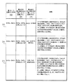
図12乃至16は、DAC及びDVC DACデバッグイベントの発生、並びに一実施形態における、例えば、DAC_OFSTビット98に対するデバッグ状態レジスタ49の更新結果を示す様々な例を表形式で示す。図12乃至16の表では、一連の3つの命令I0、I1、及びI2を各例に用いる。第1命令I0は、ロード/記憶クラスの命令であり、第2命令I1は、他に規定されない限り、ロード/記憶クラス命令であり、また、第3命令I2は、他に規定されない限り、ロード/記憶命令である。図12には、行201乃至208が含まれ、図13には、行209乃至212が含まれ、図14には、行213乃至215が含まれ、図15には、行216乃至218が含まれ、また、図16には、行219乃至220が含まれることに留意されたい。
FIGS. 12-16 illustrate in tabular form various examples illustrating the occurrence of DAC and DVC DAC debug events and the results of updating the
例を示す表の行201では、I0がDTLBエラーになり、DACデバッグイベントが起こらないと仮定する。この場合、DTLB例外が起こり、デバッグ状態レジスタは、更新されない。行202が表す例では、I0が、データ記憶割込(DSI)エラーになり、また、DACデバッグイベントが起こらない。この場合、DSI例外が生じ、デバッグ状態レジスタは、更新されない。行203が表す例では、I0が、DTLBエラーになるが、DACxデバッグイベントが示される(例えば、DAC1又はDAC2デバッグイベント)。この場合、DACxデバッグイベントに起因するデバッグ例外が発生し、また、対応するDACxビットフィールドが設定され(例えば、DAC1R、DAC1W、DAC2R、DAC2W)、IDEビット76が設定され、また、DAC_OFSTビット98が%00に設定される。DSRR0レジスタは、I0を指す(即ち、I0のアドレスを記憶する)。行204が表す例では、I0が、DSIエラーになるが、DACxデバッグイベントが示される(例えば、DAC1又はDAC2デバッグイベント)。この場合、DACxデバッグイベントに起因するデバッグ例外が発生し、また、対応するDACxビットフィールドが設定され(例えば、DAC1R、DAC1W、DAC2R、DAC2W)、IDEビット76が設定され、また、DAC_OFSTビット98が、%00に設定される。DSRR0レジスタは、I0を指す(即ち、I0のアドレスを記憶する)。行205が表す例では、I0がDACxデバッグイベント(例えば、DAC1又はDAC2デバッグイベント)を発生させる。この場合、DACxデバッグイベントに起因するデバッグ例外が発生し、また、対応するDACxビットフィールドが設定され(例えば、DAC1R、DAC1W、DAC2R、DAC2W)、DAC_OFSTビット98が、%00に設定される。DSRR0レジスタは、I1を指す(即ち、I1のアドレスを記憶する)。行203及び204に示された条件の場合、IDEビット76が設定されるが、行205の場合、IDEビット76は設定されないことに留意されたい。このことを用いて、行203及び204の%00のDAC_OFST設定値が、命令I0が割込を発生させたことを示していることが示され、また、DAC1又はDAC2イベントによりI0上でデバッグ割込が起こる時、DSRR0のセーブしたプログラムカウンタ値は、I0を指しており、通常の位置(I1)ではないことが示される。これが起こる理由は、I0上には、同時にDTLB又はDSI例外もあり、従って、I0は、実行が完了していないことから、デバッグ割込の後、再実行するべきためである。再実行時、DAC1、DAC2イベントは、ユーザによって無効にされることがあり、その場合、通常のDTLB又はDSI例外が発生し、適切に処理される。しかしながら、行205の場合、命令I0は、実行を完了しており、従って、セーブしたDSRR0値がI1を指し、DAC_OFST値が%00であり、また、IDEがクリアされ、DAC_OFST値が%00の場合のDSRR0の通常の境界条件を示す。
In
行206乃至220が表す様々な例では、I0がDVCx DACxデバッグイベント(例えば、DVC1 DAC1又はDVC2 DAC2デバッグイベントのいずれか)を発生させる。行206が表す例では、I1は、例外を起こさず、任意の命令であってよく、また、I3は、例外を起こさず、ロード/記憶型の命令ではない。この場合、DVCx DACxデバッグイベントに起因するデバッグ例外が発生し、また、対応するDACxビットフィールドが設定され(例えば、DAC1R、DAC1W、DAC2R、DAC2W)、DAC_OFSTビット98が%01に設定される。DSRR0レジスタは、I2の後の命令を指す。DAC_OFSTビット98を調べることによって、I0がDVCx DACxイベントを引き起こしたことを判定できる。
In the various examples represented by lines 206-220, I0 generates a DVCx DACx debug event (eg, either a DVC1 DAC1 or a DVC2 DAC2 debug event). In the example represented by
行207は、図9と同様な例を表し、この例では、I1が例外を起こさず、また、I3が例外を起こさないが、I3は、ロード/記憶クラス命令である。この場合、DVCx DACxデバッグイベントに起因するデバッグ例外が発生し、そして、対応するDACxビットフィールドが設定され(例えば、DAC1R、DAC1W、DAC2R、DAC2W)、DAC_OFSTビット98が%10に設定される。DSRR0レジスタは、I2の後の命令を指す。本例では、命令I2は、メモリアクセスを開始したことから、完了できるようにすべきである。行208は、図11と同様な例を表し、この例では、I1は、DTLBエラーを起こし、DACを引き起こさない。この場合、DVCx DACxデバッグイベントに起因するデバッグ例外が発生し、そして、対応するDACxビットフィールドが設定され(例えば、DAC1R、DAC1W、DAC2R、DAC2W)、DAC_OFSTビット98が%00に設定される。DSRR0レジスタは、I1が、DTLBエラーを引き起こし、実行を完了しなかったことから、I1を指す。DAC_OFSTビット98を調べることによって、I0がDVCx DACxイベントを引き起こしたことを判定できる。
行209が表す例では、I1がDSIエラーを起こし、DACを引き起こさない。この場合、DVCx DACxデバッグイベントに起因するデバッグ例外が発生し、そして、対応するDACxビットフィールドが設定され(例えば、DAC1R、DAC1W、DAC2R、DAC2W)、DAC_OFSTビット98が%00に設定される。DSRR0レジスタは、I1が、DSI例外を引き起こし、実行を完了しなかったことから、I1を指す。行210が表す例では、I1がDTLBエラー及びDACy(例えば、DAC1又はDAC2デバッグイベント)を発生させる。この場合、DVCx DACxデバッグイベントに起因するデバッグ例外が発生し、そして、対応するDACxビットフィールドが設定され(例えば、DAC1R、DAC1W、DAC2R、DAC2W)、DAC_OFSTビット98が%00に設定される。DSRR0レジスタは、I1を指す。この場合、I1のDACyイベントは、I1のDTLBエラーによりいずれにせよ再実行すべきであることから、報告されない。行211が表す例では、I1がDSIエラー及びDACy(例えば、DAC1又はDAC2デバッグイベント)を発生させる。この場合、DVCx DACxデバッグイベントに起因するデバッグ例外が発生し、そして、対応するDACxビットフィールドが設定され(例えば、DAC1R、DAC1W、DAC2R、DAC2W)、DAC_OFSTビット98が%00に設定される。DSRR0レジスタは、I1を指す。この場合、I1のDACyイベントは、I1のDTLBエラーによりいずれにせよ再実行すべきであることから、報告されない。行208乃至211の例の場合、I1例外は、マスクされるが、このことは、実施例に依存するものであり、他のプロセッサでは異なり得ることに留意されたい。
In the example represented by
行212が表す例では、I1がDACy(例えば、DAC1又はDAC2デバッグイベント)を発生させる。この場合、デバッグ例外が発生し、そして、対応するDACxビットフィールドが設定され(例えば、DAC1R、DAC1W、DAC2R、DAC2W)、対応するDACyビットフィールドが設定され(例えば、DAC1R、DAC1W、DAC2R、DAC2W)、また、DAC_OFSTビット98が%01に設定される。DSRR0レジスタは、I2を指す。行213が表す例では、I1は、DVCy DACy(例えば、DVC1 DAC1又はDVC2 DAC2デバッグイベント)を引き起こし、また、通常のロード/記憶命令であり、I2は、ロード/記憶命令ではない。この場合、デバッグ例外が発生し、そして、対応するDACxビットフィールドが設定され(例えば、DAC1R、DAC1W、DAC2R、DAC2W)、対応するDACyビットフィールドが設定され(例えば、DAC1R、DAC1W、DAC2R、DAC2W)、また、DAC_OFSTビット98が%01に設定される。DSRR0レジスタは、I2を指す。この場合、xがyに等しければ、デバッグ状態レジスタ及びDSRR0に結果的に生じる状態は、「DACyなし」の場合(即ち、I2がDACyを引き起こさない場合)と区別できなくなり得ることにも留意されたい。
In the example represented by
行214が表す例では、I1は、DVCy DACy(例えば、DVC1 DAC1又はDVC2 DAC2デバッグイベント)を引き起こし、また、通常のロード/記憶命令であり、I2は、例外を引き起こさないロード/記憶命令である。この場合、デバッグ例外は、I2がメモリアクセスを開始したことから、その完了後に発生し、そして、対応するDACxビットフィールドが設定され(例えば、DAC1R、DAC1W、DAC2R、DAC2W)、対応するDACyビットフィールドが設定され(例えば、DAC1R、DAC1W、DAC2R、DAC2W)、また、DAC_OFSTビット98が%10に設定される。DSRR0レジスタは、I2の後の命令を指す。この場合、xがyに等しければ、デバッグ状態レジスタ及びDSRR0に結果的に生じる状態は、「DACyなし」の場合(即ち、I2がDACyを引き起こさない場合)と区別できなくなり得ることにも留意されたい。
In the example represented by line 214, I1 is a DVCy DACy (eg, DVC1 DAC1 or DVC2 DAC2 debug event) and is a normal load / store instruction, and I2 is a load / store instruction that does not cause an exception. . In this case, a debug exception occurs after I2 has started memory access, and after that, and the corresponding DACx bit field is set (eg, DAC1R, DAC1W, DAC2R, DAC2W) and the corresponding DACy bitfield Is set (eg, DAC1R, DAC1W, DAC2R, DAC2W), and the
行215が表す例では、I1は、DVCy DACy(例えば、DVC1 DAC1又はDVC2 DAC2デバッグイベント)を引き起こし、また、通常のロード/記憶命令であり、I2は、DSIエラーを発生させる。行216が表す例では、I1は、DVCy DACy(例えば、DVC1 DAC1又はDVC2 DAC2デバッグイベント)を引き起こし、また、通常のロード/記憶命令であり、I2は、DTLBエラーを発生させる。これらの場合のいずれにおいても、デバッグ例外が発生し、そして、対応するDACxビットフィールドが設定され(例えば、DAC1R、DAC1W、DAC2R、DAC2W)、対応するDACyビットフィールドが設定され(例えば、DAC1R、DAC1W、DAC2R、DAC2W)、また、DAC_OFSTビット98が%01に設定される。DSRR0レジスタは、I2を指す。この場合、xがyに等しければ、デバッグ状態レジスタ及びDSRR0に結果として生じる状態は、「DACyなし」の場合(即ち、I2がDACyを引き起こさない場合)と区別できなくなり得ることにも留意されたい。更に、これらの場合、命令I2は、マスクされるが、この振舞いは、実施例に依存するものであり、他のプロセッサでは異なり得ることに留意されたい。
In the example represented by
行217が表す例では、I1は、DVCy DACy(例えば、DVC1 DAC1又はDVC2 DAC2デバッグイベント)を引き起こし、また、通常のロード/記憶命令であり、I2は、DACy又はDVCy DACyを発生させる通常のロード/記憶命令又は複数ワードのロード/記憶命令である。この場合、デバッグ例外が発生し、そして、対応するDACxビットフィールドが設定され(例えば、DAC1R、DAC1W、DAC2R、DAC2W)、対応するDACyビットフィールドが設定され(例えば、DAC1R、DAC1W、DAC2R、DAC2W)、また、DAC_OFSTビット98が%10に設定される。DSRR0レジスタは、I2の後の命令を指す。この場合、xがyに等しければ、デバッグ状態レジスタ及びDSRR0に結果として生じる状態は、「DACyなし」の場合(即ち、I1又はI2がDACyを引き起こさない場合)と区別できなくなり得ることにも留意されたい。
In the example represented by
行218が表す例では、I1は、DVCy DACy(例えば、DVC1 DAC1又はDVC2 DAC2デバッグイベント)を引き起こし、また、複数ワードのロード/記憶命令であり、I2は、任意の命令である。この場合、デバッグ例外が発生し、そして、対応するDACxビットフィールドが設定され(例えば、DAC1R、DAC1W、DAC2R、DAC2W)、対応するDACyビットフィールドが設定され(例えば、DAC1R、DAC1W、DAC2R、DAC2W)、また、DAC_OFSTビット98が%01に設定される。DSRR0レジスタは、I2を指す。この場合、I1は、複数のレジスタに読込又は書込を行うことから、I2のメモリへのアクセスを防止するのに充分な時間があり、従って、I0にDVCx DACxの条件が現れると、それをキルし得る。この場合、xがyに等しければ、デバッグ状態レジスタ及びDSRR0に結果として生じる状態は、「DACyなし」の場合(即ち、I2がDACyを引き起こさない場合)と区別できなくなり得ることにも留意されたい。
In the example represented by
行219が表す例では、I1は、任意の命令であり、また、例外を起こさず、I2は、DSIエラーを発生させる通常のロード/記憶又は複数ワードのロード/記憶命令であって、DACを発生させる場合も発生させない場合もある命令である。この場合、デバッグ例外が発生し、そして、対応するDACxビットフィールドが設定され(例えば、DAC1R、DAC1W、DAC2R、DAC2W)、対応するDACyビットフィールドが設定され(例えば、DAC1R、DAC1W、DAC2R、DAC2W)、また、DAC_OFSTビット98が%01に設定される。DSRR0レジスタは、I2を指す。この場合、命令I2は、マスクされるが、この振舞いは、実施例に依存するものであり、他のプロセッサでは異なり得ることに留意されたい。
In the example represented by
行220が表す例では、I1は、任意の命令であり、また、例外を起こさず、I2は、DACy又はDVCy DACyを発生させる通常のロード/記憶又は複数ワードのロード/記憶命令である。この場合、デバッグ例外が発生し、そして、対応するDACxビットフィールドが設定され(例えば、DAC1R、DAC1W、DAC2R、DAC2W)、対応するDACyビットフィールドが設定され(例えば、DAC1R、DAC1W、DAC2R、DAC2W)、また、DAC_OFSTビット98が%10に設定される。DSRR0レジスタは、I2の後の命令を指す。この場合、xがyに等しければ、デバッグ状態レジスタ及びDSRR0に結果として生じる状態は、「DACyなし」の場合(即ち、I2がDACyを引き起こさない場合)と区別できなくなり得ることにも留意されたい。
In the example represented by
図17は、本発明の他の実施形態に基づく、図1のデータ処理システムに関係するデバッグ状態レジスタ49の図である。図17の例では、デバッグ状態レジスタ49には、IDE(76)、ICMP(78)、BRT(80)、IAC1(82)、IAC2(84)、IAC3(86)、IAC4(88)、DAC1R(90)、DAC1W(92)、DAC2R(94)、DAC2W(96)、DAC_OFSTA(102)、OCCA(104)、DAC_OFSTB(106)、及びOCCB(108)と表記したビットフィールドが含まれる。図17の例には、更に、将来の用途のために予約し得る予約ビットフィールド110を含み得る。尚、デバッグ状態レジスタ49、並びにビットフィールドIDE(76)、ICMP(78)、BRT(80)、IAC1(82)、IAC2(84)、IAC3(86)、IAC4(88)、DAC1R(90)、DAC1W(92)、DAC2R(94)、及びDAC2W(96)に関する上記説明(例えば、図7及び8の説明等)は、図17に同様に当てはまり、従って、ここでは繰り返さない。しかしながら、図7の例と異なり、図17の例には、DAC_OFST(98)ではなく複数のDACオフセットフィールド(例えば、DAC_OFSTA(102)及びDAC_OFSTB(106))が含まれる。複数のDACオフセットフィールドを用いると、複数のオフセットを追跡することができ、この場合、各DACオフセットフィールドは、DAC_OFST(98)に関して上述したように動作し得る。しかしながら、複数のDACオフセットフィールドが存在することにより、各DACオフセットフィールド(例えば、DAC_OFSTA(102)及びDAC_OFSTB(106))は、対応する発生フィールドを有する(例えば、それぞれOCCA(104)及びOCCB(108))。
FIG. 17 is a diagram of a debug status register 49 related to the data processing system of FIG. 1, in accordance with another embodiment of the present invention. In the example of FIG. 17, the
従って、DAC_OFSTAビット102を用いると、第1DVC DAC(DVC1 DAC1又はDVC2 DAC2のいずれか)を示させた命令と、データ値ブレークポイントが起こり、DVC DAC用のデバッグ例外が発生するポイントとの間に実行した命令の数を示し得る。DAC_OFSTAビット102を用いると、DAC_OFST(98)と同様に、第1データアドレス比較デバッグ例外を起こしたロード又は記憶命令のアドレスからのセーブしたDSRR0値の「オフセット−1」を記憶し得る。上述したように、DSRR0は、デバッグセーブ復旧レジスタ0に対応し、セーブしたDSRR0値は、デバッグ割込用の復帰ポインタに対応する。このようにして、第1DVC DACを引き起こしたアドレスと、命令ストリームが中断されてデータ値ブレークポイントが発生したポイント(この場合、そのデータ値ブレークポイントが、第1DVC DAC又は他のDVC DACの結果として発生し得る)との間の期間内に幾つの命令が実行されたかを判定し得る。これによって、ユーザは、どの命令が第1DVC DACを引き起こしたかを判定し得る。一実施形態では、DAC_OFSTAビット102は、通常、%00に設定され、DVC DACが、このフィールドを%00、%01、%10、又は%11に設定するが、これは、「オフセット−1」を表す。DAC_OFSTAビット102は、既定値として通常%00に設定されることから、OCCA(104)は、第1DVC DACの発生時に設定され、DAC_OFSTAが、DVC DACオフセットを示す値を保持していることを示し得る。DAC_OFSTBビット106を用いると、従って、第2DVC DACを示させた命令と、データ値ブレークポイントが起こり、DVC DAC用のデバッグ例外が発生するポイントとの間に実行される命令の数を示し得る。DAC_OFSTBビット106を用いると、第2データアドレス比較デバッグ例外を起こしたロード又は記憶命令のアドレスからのセーブしたDSRR0値の「オフセット−1」を記憶し得る。このようにして、第2DVC DACを引き起こしたアドレスと、命令ストリームが中断されてデータ値ブレークポイントが発生したポイント(ここでもまた、そのデータ値ブレークポイントが、第1DVC DAC又は第2DVC DACの結果として発生し得る)との間の期間内に幾つの命令が実行されたかを判定し得る。一実施形態では、DAC_OFSTBビット106は、通常、%00に設定され、DVC DACが、このフィールドを%00、%01、%10、又は%11に設定するが、これは、「オフセット−1」を表す。DAC_OFSTBビット106は、通常、既定値として%00に設定されることから、OCCB(108)は、第2DVC DACの発生時に設定し得る(更に、上述したように、DVC DACに対して同時にDTLBエラー又はDSIエラーが起こる場合、DAC_OFSTビット98に関して上述したように、対応するDACオフセットビットは、%00に設定され、IDEビット76は、1に設定され得ることに留意されたい)。
Therefore, using the
従って、複数の命令が、DVC DACをもたらすことがあり、また、命令ストリームが中断されてデータ値ブレークポイントが発生するポイントにおいて、オフセットフィールドDAC_OFSTA(102)及びDAC_OFSTB(104)の各々は、対応する発生ビットが設定されていると仮定すると、命令ストリームのどの命令(1つ又は複数)が、データ値ブレークポイントをもたらし得るDVC DACを引き起こしたかを示せることに留意されたい。OCCAビット104及びOCCBビット108の双方が設定され、2つのDVC DACが発生したことを示す場合、ユーザは、どの命令が実際に各DVC DACを引き起こしたかを示すために、対応するオフセット値を用い得るが、これら2つの命令の内のどちらが(即ち、2つのDVC DACの内のどちらが)命令ストリームを中断したデータ値ブレークポイントを実際にもたらしたかについてユーザが実際に判定することが必要なこともある。
Thus, multiple instructions may result in a DVC DAC, and at the point where the instruction stream is interrupted and a data value breakpoint occurs, each of the offset fields DAC_OFSTA (102) and DAC_OFSTB (104) Note that assuming that the generation bit is set, it can indicate which instruction (s) in the instruction stream caused a DVC DAC that could result in a data value breakpoint. If both
図18は、図17について述べたように、複数のオフセットフィールドの使用方法を示すタイミング図を表す。図18の例の場合、I0乃至I4の各々は、ロード命令であり、I0は、第1DAC DVCデバッグイベント(DVCx DACx、ここで、xは、1又は2のいずれかであり得る)を発生させ、I2は、第2DAC DVCデバッグイベント(DVCy DACy、ここで、yは、1又は2のいずれかであり得る)を発生させるものと仮定する。図18は、更に、六段パイプラインについて描かれているが、他の実施形態には、例えば、異なる数の段を有する異なるパイプラインを含んでもよい。図18で参照する六段パイプライン等の命令パイプラインの動作は、当分野で公知であり、従って、本明細書では詳述しない。更に、図18には、プロセッサ12のプロセッサ・クロックに対応し得るクロック信号が含まれる。プロセッサ・クロックは、システムクロック又はプロセッサ12の一部だけに供給されるクロックであってよく、当分野で公知なように生成し得る。
FIG. 18 depicts a timing diagram illustrating how to use multiple offset fields as described with respect to FIG. In the example of FIG. 18, each of I0 through I4 is a load instruction, and I0 generates a first DAC DVC debug event (DVCx DACx, where x can be either 1 or 2). , I2 is assumed to generate a second DAC DVC debug event (DVCy DACy, where y can be either 1 or 2). Although FIG. 18 is further depicted for a six-stage pipeline, other embodiments may include, for example, different pipelines having different numbers of stages. The operation of an instruction pipeline, such as the six-stage pipeline referenced in FIG. 18, is well known in the art and therefore will not be described in detail herein. In addition, FIG. 18 includes a clock signal that may correspond to the processor clock of
図18において、I0は、クロックサイクル1においてフェッチ段に入り、クロックサイクル2においてデコード段に入り、クロックサイクル3においてEA/E0段に入り、ここでI0の有効アドレスを計算し、そして、クロックサイクル4においてmem1/E1段に入る。従って、有効アドレスは、クロックサイクル3の終わりに準備が整っており、導体35のアドレス部でデバッグ制御回路44に提供され、I0の有効アドレスとデータアドレス比較レジスタ47に記憶したDAC値(DAC1及びDAC2)との間でアドレス比較を実施できるようにする(更に、この時点で、BIU(34)によってバス20上にもアドレスを配置し得ることに留意されたい)。このDACxアドレス比較は、DACアドレス比較信号の正のパルスによって示されるように、クロックサイクル4において命令I0に対して実施され、一致が起こるが、DACアドレス比較信号は、DACxアドレス比較が実施され、一致が起こっていることを示すためにデバッグ制御回路44内でアサートされる制御信号であってよい。しかしながら、DACxは、DVCx修飾子を必要とすることから(DVCxビットの設定、例えば、DVC1ビット70又はDVC2ビット72の設定により)、デバッグイベントは、DACxアドレス比較で一致しても、まだ示されない。命令処理は、I0に関係する(I0ロード命令に応じて検索される)データが、まだデータ値比較のために利用可能でないため、継続する。次に、I0は、mem2/E2段に進み、この間、データをメモリ(例えば、図1のメモリ18等)から読み込む。この読み込んだデータは、この段の終わりで利用可能となり得る(また、例えば、バス20を介してBIU(34)によって受信される)。そして、導体35のデータ部でデバッグ制御回路44に提供され、I0に関連する読み込んだデータ値と、データ値比較レジスタ53に記憶したDVCx値との間でデータ値比較を実施できるようにする。従って、データ値比較は、DVCxデータ比較信号の正のパルスによって示されるように、次のクロックサイクルであるクロックサイクル6において実施され、一致が起こるが、DVCxデータ比較信号は、DVCデータ比較が起こっていることを示すためにデバッグ制御回路44内でアサートされる制御信号であってよい。データ値比較レジスタ53に記憶したDVCx値に一致すると、DVCx DACxデバッグイベントが示され、従って、ハードウェアは、対応する状態ビットを設定する(例えば、DAC1Rビット90又はDAC2Rビット94。I0がDAC1 DVC1を引き起こしたか又はDAC2 DVC2を引き起こしたかに依存する)。
In FIG. 18, I0 enters the fetch stage at
サイクル6内においてI0上でDVCx DACxを検出すると、DACオフセットAカウンタを0にクリアし、また、後続の各完了した命令の計数を開始できるようにすることに留意されたい(DACオフセットAカウンタは、カウンタ41に含み得る)。しかしながら、パイプラインは、I1及びI2がメモリ段(mem1及びmem2)にあるため、クロックサイクル6ではまだ中断できない。従って、I1及びI2は、メモリアクセスが開始すると、中断することはできず、完了しなければならないことから、待ち状態のデバッグ例外の更なる処理に先立って、完了しなければならない。後続のメモリアクセスは、しかしながら、DVCx DACx例外が現在待ち状態であることから、起動されない。I1及びI2の各メモリアクセスは、書き戻し段に入った後、完了と見なされる。I2(命令I1及びI2の後半)は、クロックサイクル8において書き戻し段にあり、その後、デバッグ例外が発生し、また、割込処理を開始できるように、待ち状態のデバッグ例外を処理し得ることに留意されたい。即ち、DVC1 DAC1デバッグイベントの割込処理は、クロックサイクル8の後(例えば、クロックサイクル9)まで、開始できない。DVCx DACxが検出される時点で、I3は、まだパイプラインのEA/E0段にあり、従って、キルし得ることに留意されたい。即ち、命令ストリームは、I3において中断される。実行は、従って、割込処理の完了後に、I3から再開し得る。従って、DSRR0レジスタは、I3のアドレスがデータブレークポイントデバッグ割込の復帰ポインタに対応することから、I3のアドレスを記憶し得る。デバッグ割込ハンドラのソフトウェア・ルーチンの完了に続いて、通常の実行は、割込命令からの復帰を実行することによって再開されるが、通常の(非割込)命令実行を継続するために、復帰すべき命令(この場合、I3)へのポインタとしてDSRR0にセーブした値が用いられる。
Note that detecting DVCx DACx on I0 in
DVCx DACxデバッグイベントを検出してDACオフセットAカウンタをクリアした後、後続の各命令が完了した状態で、DACオフセットAカウンタは、デバッグ例外が発生する(この時点で割込処理が起こる)まで、1ずつ増加することに留意されたい。従って、DACオフセットAカウンタは、クロックサイクル8において2まで増加し、従って、デバッグ状態レジスタ49のDAC_OFSTAビット102が%10に設定され、更に、OCCAビット104が設定される。即ち、DVCx DACxを引き起こした命令(本例では、I0)の後で且つ割込処理の前に実行される命令の数は、2であり、これは、DAC_OFSTAとして記憶される。
After detecting the DVCx DACx debug event and clearing the DAC offset A counter, with each subsequent instruction completed, the DAC offset A counter will continue until a debug exception occurs (at this point interrupt processing occurs) Note that it increases by one. Thus, the DAC offset A counter is incremented to 2 in
I2は、クロックサイクル5においてEA/E0段に入ることに留意されたい。従って、有効アドレスは、クロックサイクル5の終わりに準備が整っており、導体35のアドレス部でデバッグ制御回路44に提供され、I2の有効アドレスとデータアドレス比較レジスタ47に記憶したDAC値(DAC1及びDAC2)との間でアドレス比較を実施できるようにする(更に、この時点で、BIU(34)によってバス20上にもアドレスを配置し得ることに留意されたい)。このDACyアドレス比較は、DACyアドレス比較信号の正のパルスによって示されるように、クロックサイクル6において実施され、一致が起こるが、DACyアドレス比較信号は、DACアドレス比較が実施されて一致が起こっていることを示すためにデバッグ制御回路44内でアサートされる制御信号であってよい。しかしながら、DACyは、DVCy修飾子を必要とすることから(DVCyビット、例えば、DVC1ビット70又はDVC2ビット72の設定により)、デバッグイベントは、DACyアドレス比較で一致しても、まだ示されない。命令処理は、I2に関係する(I2ロード命令に応じて検索される)データが、まだデータ値比較のために利用可能でないため、継続する。次に、I2は、mem2/E2段に進み、この間、データをメモリ(例えば、図1のメモリ18等)から読み込む。この読み込んだデータは、この段の終わりで利用可能となり得る(また、例えば、バス20を介してBIU(34)によって受信し得る)。そして、導体35のデータ部でデバッグ制御回路44に提供され、I2に関連する読み込んだデータ値と、データ値比較レジスタ53に記憶したDVCy値との間でデータ値比較を実施できるようにする。従って、データ値比較は、DVCyデータ比較信号の正のパルスによって示されるように、次のクロックサイクルであるクロックサイクル8において実施され、一致が起こるが、DVCyデータ比較信号は、DVCデータ比較が実施されて一致が起こっていることを示すためにデバッグ制御回路44内でアサートされる制御信号であってよい。データ値比較レジスタ53に記憶したDVCy値に一致すると、DVCy DACyデバッグイベントが示され、従って、ハードウェアは、対応する状態ビット(例えば、DAC1Rビット90又はDAC2Rビット94。I2がDAC1 DVC1を引き起こしたか又はDAC2 DVC2を引き起こしたかに依存する)。
Note that I2 enters the EA / E0 stage in
サイクル8内においてI2上でDVCy DACyを検出すると、DACオフセットBカウンタを0にクリアし、また、後続の各完了した命令の計数を開始できるようにすることに留意されたい(DACオフセットBカウンタは、カウンタ41に含み得る)。パイプラインは、クロックサイクル8において、まだ中断されていない。その理由は、I0によって引き起こされたDVCx DACxに応じてデータ値ブレークポイントが発生する前に、I1及びI2の双方が完了しなければならないためである。従って、I2に対応するデータも返され、DVCy DACyがデバッグ例外の発生前に起こり得る。上述したように、命令ストリームは、サイクル8の後、I3において中断され、これは、DACオフセットBカウンタが、増加せず、デバッグ例外発生時に0のままであることを意味する。従って、デバッグ状態レジスタ49のDAC_OFSTBビット106が%00に設定され、更に、OCCBビット108が設定される(これにより、ユーザは、%00が、実際のオフセット値を示すものであって、第2DVC DACが起こらなかった場合に返される単なる既定値ではないことを知ることができる)。従って、DVCy DACyを引き起こした命令(本例では、I2)の後で且つ割込処理前に実行される命令の数は、0である。このようにして、DAC_OFSTBビット106及びOCCBビット108は、第1デバッグイベント(例えば、DVCx DACx)と、その第1デバッグイベントのデバッグ例外が起こるポイントとの間で起こるデバッグイベント(例えば、DVCy DACy)に関する情報を提供し得ることに留意されたい。
Note that upon detection of DVCy DACy on I2 within
従って、図18の例では、各々異なる命令によって引き起こされた2つのDVC DACが、サイクル8の後、デバッグ例外の発生の前に起こることに留意されたい。DAC_OFSTAビット102及びDAC_OFSTBビット104を、対応するOCCAビット104及びOCCBビット108と共に用いて、I0(命令ストリームが中断したポイントに対応する前の命令I2から更に2命令前)及びI2(命令ストリームが中断したポイントに対応する前の命令I2から更に0命令前)の各々がDVC DACを引き起こしたことが分かる。そして、ユーザは、どちらの命令が実際にデータ値ブレークポイントをもたらしたかをデコードし得る(本例では、I0であり、これが第1DVC DAC、DVCx DACxを引き起こした)。更に、I0がDVC1 DAC1又はDVC2 DAC2の1つを引き起こし、I2がDVC1 DAC1及びDVC2 DAC2の他方を発生させるように、x及びyが異なってよいことに留意されたい。他の選択肢として、I0及びI2の双方が、DVC1 DAC1又はDVC2 DAC2のいずれかを発生させるように、xがyに等しくてもよい。更に、一実施形態では、DAC Aオフセットカウンタ及びDAC Bオフセットカウンタは、オフセットカウンタ(1つ又は複数)41内に配置し得ることに留意されたい。
Therefore, note that in the example of FIG. 18, two DVC DACs, each caused by a different instruction, occur after
従って、デバッグイベントの発生とデバッグ例外の発生との間(即ち、デバッグイベントの発生とそのデバッグイベントの割込処理の開始との間)で実行する命令の数の判定を支援するために、どのように1つ又は複数のオフセット値を用いるかについて認識することができる。これによって、デバッグ処理を改善でき、ユーザは、これらの1つ又は複数のオフセット値を用いて、実際にどの命令がデバッグ例外を発生させたか良く理解できるようになる。上記の説明は、データ値ブレークポイントに帰着するDVC DACデバッグイベントに関して行ったが、これらのオフセット値(DAC_OFST、DAC_OFSTA、及びDAC_OFSTB等)は、他の種類のデバッグイベントに用いてよい。即ち、DAC_OFST、DAC_OFSTA、及びDAC_OFSTB等のオフセットフィールドは、任意の種類のデバッグイベントの発生と、対応するデバッグ例外の発生との間(即ち、任意の種類のデバッグイベント発生と、特定のデバッグイベントの割込処理開始との間)に実行する命令の数を示すために用い得る。 Therefore, to assist in determining the number of instructions to execute between the occurrence of a debug event and the occurrence of a debug exception (ie, between the occurrence of a debug event and the start of interrupt processing for that debug event) How to use one or more offset values. This can improve the debugging process and allow the user to better understand which instruction actually caused the debug exception using these one or more offset values. Although the above description has been made with respect to DVC DAC debug events that result in data value breakpoints, these offset values (DAC_OFST, DAC_OFSTA, and DAC_OFSTB, etc.) may be used for other types of debug events. That is, the offset fields such as DAC_OFST, DAC_OFSTA, and DAC_OFSTB are between the occurrence of any type of debug event and the corresponding debug exception (ie, any type of debug event occurrence and a specific debug event Can be used to indicate the number of instructions to be executed (between the start of the interrupt process).
更に、デバッグイベントを引き起こした命令の位置ではなく、そのイベントが起こってから実行される命令の数を知ることは、有用であり得ることに留意されたい。その理由は、待ち状態のデバッグイベントの場合、命令ストリームを中断できるパイプライン境界に達する前に、(同じ位置の)同じ命令を何回も実行可能であり、従って、位置情報が、それ自体では、実際の一連のイベントを判定するには不充分な場合があり得ることを理解できるためである。 Furthermore, it should be noted that it may be useful to know the number of instructions that are executed since the event occurred, rather than the location of the instruction that caused the debug event. The reason is that in the case of a waiting debug event, the same instruction (at the same location) can be executed multiple times before reaching the pipeline boundary where the instruction stream can be interrupted, so the location information by itself This is because it can be understood that it may be insufficient to determine the actual series of events.
一実施形態では、システムは、複数の命令について、フェッチ、デコード、および実行と、各命令の実行に関連した結果の書込とを連続的に行うことによって、複数の命令を実行するためのパイプライン・プロセッサと、パイプライン・プロセッサに結合されており、複数の命令の実行を監視してデバッグイベントが発生する時を判定し、デバッグ例外を発生させて命令処理フローを中断するためのデバッグ回路と、を含む。デバッグ回路は、デバッグイベントを引き起こした命令と命令実行においてデバッグ例外が発生するポイントとの間で命令実行を完了させる命令(存在する場合)の数を表す値を示すための制御回路をさらに含む。 In one embodiment, the system includes a pipe for executing a plurality of instructions by sequentially fetching, decoding, and executing the instructions and writing a result associated with the execution of each instruction. A debug circuit that is coupled to the line processor and the pipeline processor, monitors execution of multiple instructions to determine when a debug event occurs, generates a debug exception, and interrupts the instruction processing flow And including. The debug circuit further includes a control circuit for indicating a value representing the number of instructions (if any) that complete instruction execution between the instruction that caused the debug event and the point at which a debug exception occurs during instruction execution.
更なる一実施形態では、デバッグ回路の制御回路は、デバッグイベントを引き起こした命令に続き命令実行を完了させる命令の数を表す値としてカウント値を計数して与えるためのカウンタをさらに含む。更に他の実施形態では、カウント値が0より大きいことはデバッグイベントの処理が曖昧であることを示す。 In a further embodiment, the control circuit of the debug circuit further includes a counter for counting and providing a count value as a value representing the number of instructions that complete instruction execution following the instruction that caused the debug event. In yet another embodiment, a count value greater than 0 indicates that the debug event processing is ambiguous.
更なる他の実施形態では、デバッグ回路は、デバッグイベントを引き起こした命令に続き命令実行を完了させる1つ以上の追加の命令もデバッグイベントの発生を引き起こしたことを示す。 In yet another embodiment, the debug circuit indicates that one or more additional instructions that complete instruction execution following the instruction that caused the debug event also caused the occurrence of the debug event.
更なる他の実施形態では、パイプライン・プロセッサはデバッグイベントを各々引き起こす2つ以上の命令を実行し、制御回路は複数のカウンタをさらに含み、各カウンタは、デバッグイベントを引き起こす2つ以上の命令のそれぞれの命令に続き命令実行を完了させる追加の命令の数によって決定される、それぞれのカウント値を与える。 In still other embodiments, the pipeline processor executes two or more instructions that each cause a debug event, the control circuit further includes a plurality of counters, each counter including two or more instructions that cause a debug event. Each count value is given a respective count value determined by the number of additional instructions that complete instruction execution.
更なる他の実施形態では、デバッグ回路は、デバッグイベントを引き起こした命令に続き命令実行においてデバッグ例外が発生する所定のポイントまでに命令実行を完了させる追加の命令(存在する場合)の数を表す値を保持するためのフィールドを有するデバッグ状態レジスタをさらに含む。 In yet another embodiment, the debug circuit represents the number of additional instructions (if any) that complete instruction execution by a predetermined point where a debug exception occurs in instruction execution following the instruction that caused the debug event. It further includes a debug status register having a field for holding a value.
更なる他の実施形態では、デバッグ回路は、複数の命令のうちの1つのデコードを行い、パイプライン・プロセッサによって形成されたアドレスを1つ以上の所定のデバッグアドレスと比較してデータアドレス一致が発生したか否かを判定し、パイプライン・プロセッサによってアクセスの行われたデータ値を1つ以上の所定のデータ値と比較してデータ値一致が発生したか否かを判定することとに応じて、デバッグイベントが発生したことを判定し、デバッグイベントは両比較演算について一致が発生することを必要とする。 In yet another embodiment, the debug circuit decodes one of the plurality of instructions and compares the address formed by the pipeline processor with one or more predetermined debug addresses to ensure data address match. In response to determining whether a data value match has occurred by comparing the data value accessed by the pipeline processor with one or more predetermined data values. Thus, it is determined that a debug event has occurred, and the debug event requires that a match occurs for both comparison operations.
他の実施形態では、システムは、複数の命令について、フェッチ、デコード、および実行と、各命令の実行に関連した結果の書込とを連続的に行うことによって、複数の命令を実行するためのパイプライン処理回路と、パイプライン処理回路に結合されており、1つ以上のデバッグアドレスを命令実行によって形成されるアドレスと選択的に比較することと、1つ以上のデバッグデータ値を命令実行によって形成されるデータと選択的に比較することとによって、複数の命令の実行を監視するデバッグ回路と、を含む。デバッグ回路は、両方の比較が一致を生じるときを判定し、該判定に応答してデバッグイベントを示し、デバッグイベントを引き起こした命令の後に命令実行においてデータ値ブレークポイントが発生する所定のポイントまでに実行される命令の数を示す。 In other embodiments, the system is configured to execute a plurality of instructions by sequentially fetching, decoding, and executing the plurality of instructions and writing a result associated with the execution of each instruction. A pipeline processing circuit, coupled to the pipeline processing circuit, selectively comparing one or more debug addresses with an address formed by instruction execution and one or more debug data values by instruction execution And a debug circuit that monitors execution of the plurality of instructions by selectively comparing with the formed data. The debug circuit determines when both comparisons result in a match, indicates a debug event in response to the determination, and by a predetermined point at which a data value breakpoint occurs in instruction execution after the instruction that caused the debug event. Indicates the number of instructions to be executed.
他の実施形態の更なる実施形態では、データ値ブレークポイントは曖昧であり、試験回路は、曖昧なデータ値ブレークポイントが発生したか否かを示すビットフィールドを有するレジスタをさらに含む。 In a further embodiment of another embodiment, the data value breakpoint is ambiguous and the test circuit further includes a register having a bit field that indicates whether an ambiguous data value breakpoint has occurred.
他の実施形態の更なる他の実施形態では、試験回路は、デバッグイベントが発生する時とデータ値ブレークポイントが発生する時との間に発生するイベントに関する状態情報を示すための状態レジスタをさらに含む。更に他の実施形態では、デバッグイベントが発生する時とデータ値ブレークポイントが発生する時との間に発生するイベントのうちの1つは、第2のデバッグイベントをさらに含む。 In yet another embodiment of the other embodiment, the test circuit further includes a status register for indicating status information regarding an event that occurs between when the debug event occurs and when the data value breakpoint occurs. Including. In yet another embodiment, one of the events that occurs between when the debug event occurs and when the data value breakpoint occurs further includes a second debug event.
他の実施形態の更なる他の実施形態では、デバッグ回路は、デバッグイベントを引き起こした命令に続き命令実行を完了させる命令の数のカウント値を計数して与えるためのカウンタをさらに含む。 In yet another embodiment of the other embodiments, the debug circuit further includes a counter for counting and providing a count value of the number of instructions that complete instruction execution following the instruction that caused the debug event.
他の実施形態の更なる他の実施形態では、デバッグ回路は、デバッグイベントを引き起こした命令に続き、命令実行においてデータ値ブレークポイントが発生する所定のポイントまでに命令実行を完了させる追加の命令(存在する場合)の数を示す値を保持するためのフィールドを有する状態デバッグレジスタをさらに含む。 In yet another embodiment of other embodiments, the debug circuit includes an additional instruction (following the instruction that caused the debug event, which completes the instruction execution by a predetermined point where a data value breakpoint occurs in the instruction execution. It further includes a state debug register having a field for holding a value indicating the number (if any).
更に他の実施形態では、方法は、複数の命令について、フェッチ、デコード、および実行と、各命令の実行に関連した結果の書込とを連続的に行うことによって、複数の命令を実行する工程と、複数の命令の実行を監視してデバッグイベントが発生する時を判定する工程と、デバッグ例外を発生させて命令処理フローを中断する工程と、デバッグイベントを引き起こした命令と命令実行においてデバッグ例外が発生するポイントとの間で命令実行を完了させる命令(存在する場合)の数を示す工程と、を含む。 In yet another embodiment, the method executes the plurality of instructions by sequentially fetching, decoding, and executing the plurality of instructions and writing a result associated with the execution of each instruction. Monitoring the execution of multiple instructions to determine when a debug event occurs, generating a debug exception and interrupting the instruction processing flow, and the instruction that caused the debug event and the debug exception in the instruction execution Indicating the number of instructions (if any) that complete instruction execution with the point at which the occurrence occurs.
更に他の実施形態の更なる実施形態では、方法は、デバッグイベントを引き起こした命令に続き命令実行を完了させる命令の数のカウント値を計数して与える工程をさらに含む。更なる実施形態では、方法は、デバッグイベントの処理が曖昧であることを示す0より大きいカウント値を形成する工程をさらに含む。 In a further embodiment of yet another embodiment, the method further includes counting and providing a count value of the number of instructions that complete instruction execution following the instruction that caused the debug event. In a further embodiment, the method further includes forming a count value greater than zero indicating that processing of the debug event is ambiguous.
他の実施形態の更なる他の実施形態では、方法は、デバッグイベントを引き起こした命令に続き命令実行を完了させる1つ以上の追加の命令もデバッグイベントの発生を引き起こしたことを判定する工程をさらに含む。 In still other embodiments of other embodiments, the method includes determining that one or more additional instructions that complete instruction execution following the instruction that caused the debug event also caused the occurrence of the debug event. In addition.
他の実施形態の更なる他の実施形態では、方法は、2つ以上の命令が各々デバッグイベントを引き起こすことを判定する工程と、2つ以上の命令の各々に続き命令実行を完了させる追加の命令の数のそれぞれのカウント値を異なるカウンタに記憶する工程と、をさらに含む。 In still other embodiments of other embodiments, the method includes determining that two or more instructions each cause a debug event and an additional to complete instruction execution following each of the two or more instructions. Storing each count value of the number of instructions in a different counter.
他の実施形態の更なる他の実施形態では、方法は、デバッグ回路にデバッグ状態レジスタを与える工程と、状態レジスタは、デバッグイベントを引き起こした命令に続き命令実行においてデバッグ例外が発生する所定のポイントまでに命令実行を完了させる追加の命令(存在する場合)の数を示すための値を保持するためのフィールドを有することと、をさらに含む。 In yet another embodiment of another embodiment, the method includes providing a debug status register to the debug circuit, and the status register includes a predetermined point at which a debug exception occurs in instruction execution following the instruction that caused the debug event. Further comprising having a field to hold a value to indicate the number of additional instructions (if any) to complete instruction execution.
他の実施形態の更なる他の実施形態では、方法は、複数の命令のうちの1つのデコードを行うことに応答して、デバッグイベントが発生したと判定する工程と、パイプライン・プロセッサによって形成されるアドレスを1つ以上の所定のデバッグアドレスと比較してデータアドレス一致が発生したか否かを判定する工程と、パイプライン・プロセッサによって形成されるデータ値を1つ以上の所定のデータ値と比較してデータ値一致が発生したか否かを判定する工程と、デバッグイベントは両比較演算について一致が発生することを必要とすることと、をさらに含む。 In yet another embodiment of the other embodiments, a method is provided for determining that a debug event has occurred in response to performing decoding of one of a plurality of instructions and formed by a pipeline processor. Comparing the address to be compared with one or more predetermined debug addresses to determine whether a data address match has occurred, and the data value formed by the pipeline processor to be one or more predetermined data values And determining whether a data value match has occurred and the debug event requires a match to occur for both comparison operations.
本発明を実装する装置は、ほとんど当業者には既知の電子部品や回路から構成されるため、回路の詳細については、本発明の根底にある概念の理解や認識のために、また、本発明の教示内容が不明瞭になったり注意が逸れたりしないように、上述した如く必要と思われる以上の説明はしない。 Since the apparatus for implementing the present invention is mostly composed of electronic components and circuits known to those skilled in the art, the details of the circuit are described in order to understand and recognize the concept underlying the present invention, and the present invention. In order not to obscure the contents of the teachings or to distract attention, no further explanation will be given as it seems necessary.
本明細書に用いる用語「プログラム」は、コンピュータシステム上での実行用に設計された一連の命令と定義する。プログラム、即ち、コンピュータプログラムには、サブルーチン、関数、手順、オブジェクト・メソッド、オブジェクト実装、実行可能なアプリケーション、アプレット、サーブレット、ソースコード、オブジェクトコード、共有ライブラリ/動的読込ライブラリ、及び/又はコンピュータシステム上での実行用に設計された他の一連の命令を含み得る。 The term “program” as used herein is defined as a series of instructions designed for execution on a computer system. Programs, ie computer programs, include subroutines, functions, procedures, object methods, object implementations, executable applications, applets, servlets, source code, object code, shared libraries / dynamically loaded libraries, and / or computer systems Other series of instructions designed for execution above may be included.
上述した実施形態の一部は、適用可能であれば、様々な異なる情報処理システムを用いて実現し得る。例えば、図1及びそれについての説明では、代表的な情報処理構成について述べるが、この代表的な構成は、本発明の様々な態様の説明において有用な基準を提供するためだけに示している。勿論、構成の説明は、説明のために簡素化しており、また、この構成は、本発明に基づいて用い得る多くの異なる種類の適切な構成の内の1つに過ぎない。当業者は、論理ブロック間の境界は、説明のためだけであり、他の実施形態では、論理ブロック又は回路素子を併合したり、様々な論理ブロック又は回路素子に機能を分解して代替させたりしてよいことを認識されるであろう。 Some of the above-described embodiments can be realized using various different information processing systems if applicable. For example, in FIG. 1 and the description thereof, a representative information processing arrangement is described, which is shown only to provide a useful reference in the description of various aspects of the present invention. Of course, the description of the configuration has been simplified for purposes of illustration, and this configuration is only one of many different types of suitable configurations that can be used in accordance with the present invention. Those skilled in the art will recognize that the boundaries between logic blocks are for illustrative purposes only; in other embodiments, the logic blocks or circuit elements may be merged, or the various logic blocks or circuit elements may be functionally replaced. It will be recognized that
従って、本明細書に示した構成は代表例に過ぎず、実際には、同じ機能を実現する任意の他の構成を実装し得ることを理解されたい。抽象的ではあるが明確に、同じ機能を達成する構成要素の任意の構成は、所望の機能を達成するように有効に「関連付けられる」。従って、本明細書において特定の機能を達成するために組み合わせた任意の2つの構成要素は、構成又は中間構成要素にかかわらず、所望の機能を達成するように互いに「関連付けられている」と理解し得る。同様に、そのように関連付けた任意の2つの構成要素は、所望の機能を達成するために互いに「動作可能に接続された」又は「動作可能に結合された」とも見なし得る。 Thus, it should be understood that the configurations shown herein are merely representative, and in fact any other configuration that implements the same function may be implemented. Clearly, but abstractly, any configuration of components that accomplish the same function is effectively “associated” to achieve the desired function. Thus, any two components combined to accomplish a particular function herein are understood to be "associated" with each other to achieve the desired function, regardless of configuration or intermediate components. Can do. Similarly, any two components so associated may also be considered “operably connected” or “operably coupled” to each other to achieve a desired function.
更に、例えば、一実施形態では、システム10の図示した要素は、単一の集積回路上又は同一装置内に配置された回路である。他の選択肢として、システム10には、相互接続された任意の数の別個の集積回路又は別個の装置を含み得る。更に、例えば、システム10又はその一部は、物理的な回路又は物理的な回路に転換可能な論理表現のソフト又はコード表現であってよい。このように、システム10は、任意の適切な種類のハードウェア記述言語で具現化し得る。
Further, for example, in one embodiment, the illustrated elements of
更に、当業者は、上述した動作の機能間の境界は、単なる例示であることを認識されるであろう。複数動作の機能は、単一動作に集約してもよく、及び/又は単一動作の機能は、追加の動作に分散してもよい。更に、他の実施形態には、特定の動作の複数のインスタンスを含んでもよく、動作順序は、様々な他の実施形態では、変更してもよい。 Furthermore, those skilled in the art will recognize that the boundaries between the functions of operation described above are merely exemplary. Multiple operation functions may be aggregated into a single operation, and / or single operation functions may be distributed over additional operations. Furthermore, other embodiments may include multiple instances of a particular operation, and the order of operations may be changed in various other embodiments.
本明細書に述べたソフトウェアの全て又は一部は、データ処理システム10の受信される要素であってよく、例えば、メモリ18等のコンピュータ判読可能媒体又は他のコンピュータシステム上の他の媒体から受信し得る。そのようなコンピュータ判読可能媒体は、データ処理システム10等の情報処理システムに、恒久的に、着脱可能に、又は遠隔的に結合してよい。コンピュータ判読可能媒体には、例えば、これらに限定するものではないが、ほんの一例を挙げると、ディスク及びテープ記憶媒体を含む磁気記憶媒体と、コンパクトディスク媒体(例えば、CD−ROM、CD−R等)及びデジタル映像ディスク記憶媒体等の光学記憶媒体と、FLASHメモリ、EEPROM、EPROM、ROM等の半導体ベースのメモリユニットを含む不揮発性メモリ記憶媒体と、強磁性デジタルメモリと、MRAMと、レジスタ、バッファ又はキャッシュ、主記憶装置、RAM等を含む揮発性記憶媒体と、コンピュータネットワーク、二地点間電気通信設備、及び搬送波伝送媒体を含むデータ伝送媒体と、の内から任意の数のものを含んでよい。
All or part of the software described herein may be a received element of the
本発明について、本明細書では特定の実施形態を参照して述べたが、様々な修正や変更は、以下の請求項に記載した本発明の範囲から逸脱することなく行い得る。従って、明細書及び図は、限定的であるというよりもむしろ例示であると解釈すべきであり、また、そのような全ての修正は、本発明の範囲内に含まれるものとする。本明細書において具体的な実施形態に関して述べたあらゆる恩恵、利点、又は問題に対する解決策も、全ての請求項の不可欠、必須、又は本質的な特徴もしくは要素であると解釈しようとするものではない。 Although the invention has been described herein with reference to particular embodiments, various modifications and changes can be made without departing from the scope of the invention as set forth in the claims below. The specification and drawings are accordingly to be regarded as illustrative rather than restrictive, and all such modifications are intended to be included within the scope of the present invention. Any benefit, advantage, or solution to a problem described herein with respect to a particular embodiment is not intended to be interpreted as an essential, essential, or essential feature or element of every claim. .
本明細書に用いた用語「結合された」は、直接結合又は機械的結合に限定するものではない。
更に、本明細書に用いた用語「a又はan(不定冠詞)」は、1つ又は2つ以上と定義する。更に、請求項において「少なくとも1つの」及び「1つ又は複数の」等の導入節を用いることは、不定冠詞「a」又は「an」による他の請求項要素の導入が、同じ請求項に導入節「1つ又は複数の」又は「少なくとも1つの」及び「a」又は「an」等の不定冠詞が含まれる場合でも、そのように導入した請求項要素を含む任意の特定の請求項を、そのような要素を1つだけ含む発明に限定することを意味すると解釈すべきではない。同じことは、定冠詞の使用にも当てはまる。
The term “coupled” as used herein is not limited to direct or mechanical coupling.
Furthermore, the term “a or an” (an indefinite article) as used herein is defined as one or more. Furthermore, the use of introductory clauses such as “at least one” and “one or more” in a claim means that the introduction of other claim elements by the indefinite article “a” or “an” Any particular claim including claim elements so introduced, even if the introductory clause "one or more" or "at least one" and indefinite articles such as "a" or "an" are included Should not be construed to mean limited to the invention comprising only one such element. The same applies to the use of definite articles.
特に明記しない限り、「第1」及び「第2」等の用語は、そのような用語が述べる要素間を任意に区別するために用いる。従って、これらの用語は、必ずしもそのような要素の時間的な又は他の優先順位付けを示そうとするものではない。 Unless stated otherwise, terms such as “first” and “second” are used to arbitrarily distinguish between the elements such terms describe. Thus, these terms are not necessarily intended to indicate temporal or other prioritization of such elements.
Claims (5)
前記パイプライン・プロセッサに結合されており、前記複数の命令の実行を監視してデバッグイベントが発生する時を判定し、デバッグ例外を発生させて命令処理フローを中断するためのデバッグ回路と、を含むシステムであって、前記デバッグ回路は、前記デバッグイベントの発生から該デバッグイベントの発生に応じたデバッグ例外の発生までに書き戻しによって完了する命令の数のカウントを行うための制御回路をさらに含む、システム。 A pipeline processor for executing a plurality of instructions by sequentially fetching, decoding, and executing the plurality of instructions and writing a result associated with the execution of each instruction;
A debug circuit coupled to the pipeline processor for monitoring execution of the plurality of instructions to determine when a debug event occurs, and generating a debug exception to interrupt the instruction processing flow; The debug circuit further includes a control circuit for counting the number of instructions that are completed by writing back from the occurrence of the debug event to the occurrence of a debug exception according to the occurrence of the debug event. ,system.
前記デバッグイベントの発生から前記デバッグ例外の発生までに書き戻しによって完了する命令の数のカウントとしてカウント値を計数して与えるためのカウンタをさらに含む請求項1に記載のシステム。 The control circuit of the debug circuit is:
The system of claim 1, further comprising a counter for counting and providing a count value as a count of the number of instructions completed by rewriting from the occurrence of the debug event until the occurrence of the debug exception.
前記パイプライン処理回路に結合されており、1つ以上のデバッグアドレスを命令実行によって形成されるアドレスと選択的に比較することと、1つ以上のデバッグデータ値を命令実行によって形成されるデータと選択的に比較することとによって、前記複数の命令の実行を監視するデバッグ回路と、を含むシステムであって、前記デバッグ回路は、両方の比較が一致を生じるときを判定し、該判定に応答してデバッグイベントの発生を示すことと、前記デバッグ回路は、前記デバッグイベントの発生から該デバッグイベントの発生に応じたデータ値ブレークポイントの発生までに実行される命令の数のカウントを行う、システム。 A pipeline processing circuit for executing a plurality of instructions by sequentially fetching, decoding, and executing the plurality of instructions and writing a result related to the execution of each instruction;
Coupled to the pipeline processing circuit, selectively comparing one or more debug addresses with an address formed by instruction execution, and one or more debug data values formed by instruction execution; A debug circuit that monitors execution of the plurality of instructions by selectively comparing, wherein the debug circuit determines when both comparisons produce a match and responds to the determination Indicating the occurrence of a debug event, and the debug circuit counts the number of instructions executed from the occurrence of the debug event to the occurrence of a data value breakpoint according to the occurrence of the debug event. .
Applications Claiming Priority (3)
| Application Number | Priority Date | Filing Date | Title |
|---|---|---|---|
| US11/864,292 | 2007-09-28 | ||
| US11/864,292 US8407457B2 (en) | 2007-09-28 | 2007-09-28 | System and method for monitoring debug events |
| PCT/US2008/072109 WO2009045628A1 (en) | 2007-09-28 | 2008-08-04 | System and method for monitoring debug events |
Publications (3)
| Publication Number | Publication Date |
|---|---|
| JP2010541067A JP2010541067A (en) | 2010-12-24 |
| JP2010541067A5 JP2010541067A5 (en) | 2011-09-22 |
| JP5419103B2 true JP5419103B2 (en) | 2014-02-19 |
Family
ID=40509716
Family Applications (1)
| Application Number | Title | Priority Date | Filing Date |
|---|---|---|---|
| JP2010526984A Expired - Fee Related JP5419103B2 (en) | 2007-09-28 | 2008-08-04 | System and method for monitoring debug events |
Country Status (4)
| Country | Link |
|---|---|
| US (1) | US8407457B2 (en) |
| JP (1) | JP5419103B2 (en) |
| CN (1) | CN101809542B (en) |
| WO (1) | WO2009045628A1 (en) |
Families Citing this family (18)
| Publication number | Priority date | Publication date | Assignee | Title |
|---|---|---|---|---|
| US9417987B2 (en) * | 2008-06-12 | 2016-08-16 | International Business Machines Corporation | Advisory warning and workaround indications to user when stopped between load and store conditional instructions while using source level debuggers |
| CN101826052B (en) * | 2010-05-04 | 2012-07-04 | 中国人民解放军国防科学技术大学 | Implementation method of break point for maintaining time-delay consistency in NUAL (Non-unit Assumed Operation Latencies) execution semantic microprocessor |
| DE102011110151B4 (en) * | 2011-08-16 | 2018-07-26 | Texas Instruments Deutschland Gmbh | A semiconductor device and method for operating a pipeline equalizer in a semiconductor device |
| KR101991680B1 (en) * | 2012-01-25 | 2019-06-21 | 삼성전자 주식회사 | Hardware debugging apparatus and method of software pipelined program |
| US9170920B2 (en) * | 2013-03-26 | 2015-10-27 | International Business Machines Corporation | Identifying and tagging breakpoint instructions for facilitation of software debug |
| US9619214B2 (en) | 2014-08-13 | 2017-04-11 | International Business Machines Corporation | Compiler optimizations for vector instructions |
| US9588746B2 (en) | 2014-12-19 | 2017-03-07 | International Business Machines Corporation | Compiler method for generating instructions for vector operations on a multi-endian processor |
| US10169014B2 (en) | 2014-12-19 | 2019-01-01 | International Business Machines Corporation | Compiler method for generating instructions for vector operations in a multi-endian instruction set |
| US10686539B2 (en) * | 2015-05-29 | 2020-06-16 | Avago Technologies International Sales Pte. Limited | Flexible debug observation point insertion in pipeline designs |
| US9880821B2 (en) | 2015-08-17 | 2018-01-30 | International Business Machines Corporation | Compiler optimizations for vector operations that are reformatting-resistant |
| US9594668B1 (en) * | 2015-09-04 | 2017-03-14 | International Business Machines Corporation | Debugger display of vector register contents after compiler optimizations for vector instructions |
| US10222775B2 (en) * | 2015-11-30 | 2019-03-05 | Hubbell Incorporated | Interrupt exception window protocol on a data communication bus and methods and apparatuses for using same |
| CN105760321B (en) * | 2016-02-29 | 2019-08-13 | 福州瑞芯微电子股份有限公司 | The debug clock domain circuit of SOC chip |
| CN106126360B (en) * | 2016-06-28 | 2020-08-25 | 海信视像科技股份有限公司 | Address hole shielding method and device |
| CN108460296A (en) * | 2016-12-09 | 2018-08-28 | 上海新微技术研发中心有限公司 | SOC chip with debugging interface security mechanism and method |
| KR102396448B1 (en) | 2017-10-19 | 2022-05-11 | 삼성전자주식회사 | Nonvolatile memory device and operation method thereof |
| US11256605B2 (en) | 2017-10-19 | 2022-02-22 | Samsung Electronics Co., Ltd. | Nonvolatile memory device |
| US11599445B2 (en) * | 2018-06-15 | 2023-03-07 | Board Of Regents, The University Of Texas System | Watcher: precise and fully-automatic on-site failure diagnosis |
Family Cites Families (24)
| Publication number | Priority date | Publication date | Assignee | Title |
|---|---|---|---|---|
| JPS62239238A (en) | 1986-04-10 | 1987-10-20 | Nec Corp | Break circuit |
| US5257358A (en) * | 1989-04-18 | 1993-10-26 | Nec Electronics, Inc. | Method for counting the number of program instruction completed by a microprocessor |
| JPH06139107A (en) * | 1992-10-30 | 1994-05-20 | Nec Corp | Brake address detecting circuit |
| US5850562A (en) * | 1994-06-27 | 1998-12-15 | International Business Machines Corporation | Personal computer apparatus and method for monitoring memory locations states for facilitating debugging of post and BIOS code |
| JP2752592B2 (en) * | 1994-12-28 | 1998-05-18 | 日本ヒューレット・パッカード株式会社 | Microprocessor, signal transmission method between microprocessor and debug tool, and tracing method |
| DE69616917T2 (en) * | 1995-08-30 | 2002-06-06 | Motorola Inc | Data processor with built-in emulation circuit |
| US5889981A (en) * | 1996-05-07 | 1999-03-30 | Lucent Technologies Inc. | Apparatus and method for decoding instructions marked with breakpoint codes to select breakpoint action from plurality of breakpoint actions |
| GB9626401D0 (en) * | 1996-12-19 | 1997-02-05 | Sgs Thomson Microelectronics | Diagnostic procedures in an integrated circuit device |
| JP3397230B2 (en) * | 1997-05-28 | 2003-04-14 | 松下電器産業株式会社 | Debug system |
| US6356960B1 (en) * | 1997-10-29 | 2002-03-12 | Sgs-Thomson Microelectronics Limited | Microprocessor having an on-chip CPU fetching a debugging routine from a memory in an external debugging device in response to a control signal received through a debugging port |
| US6016555A (en) * | 1997-11-19 | 2000-01-18 | Texas Instruments Incorporated | Non-intrusive software breakpoints in a processor instruction execution pipeline |
| US6321331B1 (en) * | 1998-04-22 | 2001-11-20 | Transwitch Corporation | Real time debugger interface for embedded systems |
| DE19835610A1 (en) * | 1998-08-06 | 2000-02-10 | Siemens Ag | Program-controlled unit and method for debugging the same |
| US6389557B1 (en) * | 1998-09-16 | 2002-05-14 | Advanced Micro Devices, Inc. | Freezing mechanism for debugging |
| JP2001134461A (en) * | 1999-11-05 | 2001-05-18 | Fujitsu Ltd | System and method for controlling reset |
| US6591378B1 (en) * | 2000-02-22 | 2003-07-08 | Motorola, Inc. | Debug controller in a data processor and method therefor |
| JP2002163126A (en) * | 2000-11-28 | 2002-06-07 | Nec Microsystems Ltd | Event detecting circuit embedded in debugging cpu, event detecting method, and external peripheral circuit |
| US6829701B2 (en) * | 2000-12-15 | 2004-12-07 | Intel Corporation | Watchpoint engine for a pipelined processor |
| US6862694B1 (en) * | 2001-10-05 | 2005-03-01 | Hewlett-Packard Development Company, L.P. | System and method for setting and executing breakpoints |
| US7051197B2 (en) * | 2002-11-22 | 2006-05-23 | Texas Instruments Incorporated | Tracing through reset |
| US7275148B2 (en) | 2003-09-08 | 2007-09-25 | Freescale Semiconductor, Inc. | Data processing system using multiple addressing modes for SIMD operations and method thereof |
| US20050188186A1 (en) * | 2004-02-23 | 2005-08-25 | Wolczko Mario I. | Obtaining execution path information in an instruction sampling system |
| US7249285B2 (en) * | 2004-03-25 | 2007-07-24 | International Business Machines Corporation | Address watch breakpoints in a hardware synchronization range |
| US7334161B2 (en) * | 2004-04-30 | 2008-02-19 | Arm Limited | Breakpoint logic unit, debug logic and breakpoint method for a data processing apparatus |
-
2007
- 2007-09-28 US US11/864,292 patent/US8407457B2/en not_active Expired - Fee Related
-
2008
- 2008-08-04 WO PCT/US2008/072109 patent/WO2009045628A1/en active Application Filing
- 2008-08-04 JP JP2010526984A patent/JP5419103B2/en not_active Expired - Fee Related
- 2008-08-04 CN CN2008801089547A patent/CN101809542B/en not_active Expired - Fee Related
Also Published As
| Publication number | Publication date |
|---|---|
| US8407457B2 (en) | 2013-03-26 |
| WO2009045628A1 (en) | 2009-04-09 |
| CN101809542A (en) | 2010-08-18 |
| JP2010541067A (en) | 2010-12-24 |
| CN101809542B (en) | 2013-06-19 |
| US20090089547A1 (en) | 2009-04-02 |
Similar Documents
| Publication | Publication Date | Title |
|---|---|---|
| JP5419103B2 (en) | System and method for monitoring debug events | |
| US7681078B2 (en) | Debugging a processor through a reset event | |
| JP5335887B2 (en) | Debugging method, control method, and debugging device for authenticating conditional debug instruction based on address | |
| US9575816B2 (en) | Deadlock/livelock resolution using service processor | |
| US9201749B2 (en) | Diagnosing code using single step execution | |
| US11513804B2 (en) | Pipeline flattener with conditional triggers | |
| US7991985B2 (en) | System and method for implementing and utilizing a zero overhead loop | |
| JP2011501265A (en) | Debug instructions for use in data processing systems | |
| KR20110044790A (en) | Debug instruction for use in a multi-threaded data processing system | |
| US7607047B2 (en) | Method and system of identifying overlays | |
| US7870430B2 (en) | Method and apparatus for sharing debug resources | |
| US6760864B2 (en) | Data processing system with on-chip FIFO for storing debug information and method therefor | |
| US20080155236A1 (en) | System and method for implementing a zero overhead loop | |
| KR20200088760A (en) | Checksum generation | |
| US11294787B2 (en) | Apparatus and method for controlling assertion of a trigger signal to processing circuitry | |
| US10747647B2 (en) | Method, apparatus and system for diagnosing a processor executing a stream of instructions | |
| GB2380831A (en) | Debug exception handler and registers | |
| WO2003034224A2 (en) | Debug exception registers |
Legal Events
| Date | Code | Title | Description |
|---|---|---|---|
| A521 | Written amendment |
Free format text: JAPANESE INTERMEDIATE CODE: A523 Effective date: 20110804 |
|
| A621 | Written request for application examination |
Free format text: JAPANESE INTERMEDIATE CODE: A621 Effective date: 20110804 |
|
| RD04 | Notification of resignation of power of attorney |
Free format text: JAPANESE INTERMEDIATE CODE: A7424 Effective date: 20120227 |
|
| A977 | Report on retrieval |
Free format text: JAPANESE INTERMEDIATE CODE: A971007 Effective date: 20121228 |
|
| A131 | Notification of reasons for refusal |
Free format text: JAPANESE INTERMEDIATE CODE: A131 Effective date: 20130108 |
|
| A521 | Written amendment |
Free format text: JAPANESE INTERMEDIATE CODE: A523 Effective date: 20130408 |
|
| A131 | Notification of reasons for refusal |
Free format text: JAPANESE INTERMEDIATE CODE: A131 Effective date: 20130618 |
|
| A521 | Written amendment |
Free format text: JAPANESE INTERMEDIATE CODE: A523 Effective date: 20130910 |
|
| TRDD | Decision of grant or rejection written | ||
| A01 | Written decision to grant a patent or to grant a registration (utility model) |
Free format text: JAPANESE INTERMEDIATE CODE: A01 Effective date: 20131022 |
|
| A61 | First payment of annual fees (during grant procedure) |
Free format text: JAPANESE INTERMEDIATE CODE: A61 Effective date: 20131113 |
|
| R150 | Certificate of patent or registration of utility model |
Ref document number: 5419103 Country of ref document: JP Free format text: JAPANESE INTERMEDIATE CODE: R150 |
|
| R250 | Receipt of annual fees |
Free format text: JAPANESE INTERMEDIATE CODE: R250 |
|
| S533 | Written request for registration of change of name |
Free format text: JAPANESE INTERMEDIATE CODE: R313533 |
|
| R250 | Receipt of annual fees |
Free format text: JAPANESE INTERMEDIATE CODE: R250 |
|
| R350 | Written notification of registration of transfer |
Free format text: JAPANESE INTERMEDIATE CODE: R350 |
|
| R250 | Receipt of annual fees |
Free format text: JAPANESE INTERMEDIATE CODE: R250 |
|
| LAPS | Cancellation because of no payment of annual fees |