JP5392190B2 - Substrate processing system and substrate processing method - Google Patents
Substrate processing system and substrate processing method Download PDFInfo
- Publication number
- JP5392190B2 JP5392190B2 JP2010126034A JP2010126034A JP5392190B2 JP 5392190 B2 JP5392190 B2 JP 5392190B2 JP 2010126034 A JP2010126034 A JP 2010126034A JP 2010126034 A JP2010126034 A JP 2010126034A JP 5392190 B2 JP5392190 B2 JP 5392190B2
- Authority
- JP
- Japan
- Prior art keywords
- processing
- carrier
- substrate
- devices
- lot
- Prior art date
- Legal status (The legal status is an assumption and is not a legal conclusion. Google has not performed a legal analysis and makes no representation as to the accuracy of the status listed.)
- Active
Links
Images


Classifications
-
- H—ELECTRICITY
- H01—ELECTRIC ELEMENTS
- H01L—SEMICONDUCTOR DEVICES NOT COVERED BY CLASS H10
- H01L21/00—Processes or apparatus adapted for the manufacture or treatment of semiconductor or solid state devices or of parts thereof
- H01L21/67—Apparatus specially adapted for handling semiconductor or electric solid state devices during manufacture or treatment thereof; Apparatus specially adapted for handling wafers during manufacture or treatment of semiconductor or electric solid state devices or components ; Apparatus not specifically provided for elsewhere
- H01L21/67005—Apparatus not specifically provided for elsewhere
- H01L21/67242—Apparatus for monitoring, sorting or marking
- H01L21/67276—Production flow monitoring, e.g. for increasing throughput
-
- H—ELECTRICITY
- H01—ELECTRIC ELEMENTS
- H01L—SEMICONDUCTOR DEVICES NOT COVERED BY CLASS H10
- H01L21/00—Processes or apparatus adapted for the manufacture or treatment of semiconductor or solid state devices or of parts thereof
- H01L21/67—Apparatus specially adapted for handling semiconductor or electric solid state devices during manufacture or treatment thereof; Apparatus specially adapted for handling wafers during manufacture or treatment of semiconductor or electric solid state devices or components ; Apparatus not specifically provided for elsewhere
- H01L21/677—Apparatus specially adapted for handling semiconductor or electric solid state devices during manufacture or treatment thereof; Apparatus specially adapted for handling wafers during manufacture or treatment of semiconductor or electric solid state devices or components ; Apparatus not specifically provided for elsewhere for conveying, e.g. between different workstations
- H01L21/67739—Apparatus specially adapted for handling semiconductor or electric solid state devices during manufacture or treatment thereof; Apparatus specially adapted for handling wafers during manufacture or treatment of semiconductor or electric solid state devices or components ; Apparatus not specifically provided for elsewhere for conveying, e.g. between different workstations into and out of processing chamber
- H01L21/67745—Apparatus specially adapted for handling semiconductor or electric solid state devices during manufacture or treatment thereof; Apparatus specially adapted for handling wafers during manufacture or treatment of semiconductor or electric solid state devices or components ; Apparatus not specifically provided for elsewhere for conveying, e.g. between different workstations into and out of processing chamber characterized by movements or sequence of movements of transfer devices
-
- H—ELECTRICITY
- H01—ELECTRIC ELEMENTS
- H01L—SEMICONDUCTOR DEVICES NOT COVERED BY CLASS H10
- H01L21/00—Processes or apparatus adapted for the manufacture or treatment of semiconductor or solid state devices or of parts thereof
- H01L21/67—Apparatus specially adapted for handling semiconductor or electric solid state devices during manufacture or treatment thereof; Apparatus specially adapted for handling wafers during manufacture or treatment of semiconductor or electric solid state devices or components ; Apparatus not specifically provided for elsewhere
- H01L21/677—Apparatus specially adapted for handling semiconductor or electric solid state devices during manufacture or treatment thereof; Apparatus specially adapted for handling wafers during manufacture or treatment of semiconductor or electric solid state devices or components ; Apparatus not specifically provided for elsewhere for conveying, e.g. between different workstations
- H01L21/67763—Apparatus specially adapted for handling semiconductor or electric solid state devices during manufacture or treatment thereof; Apparatus specially adapted for handling wafers during manufacture or treatment of semiconductor or electric solid state devices or components ; Apparatus not specifically provided for elsewhere for conveying, e.g. between different workstations the wafers being stored in a carrier, involving loading and unloading
- H01L21/67778—Apparatus specially adapted for handling semiconductor or electric solid state devices during manufacture or treatment thereof; Apparatus specially adapted for handling wafers during manufacture or treatment of semiconductor or electric solid state devices or components ; Apparatus not specifically provided for elsewhere for conveying, e.g. between different workstations the wafers being stored in a carrier, involving loading and unloading involving loading and unloading of wafers
Landscapes
- Engineering & Computer Science (AREA)
- Physics & Mathematics (AREA)
- Condensed Matter Physics & Semiconductors (AREA)
- General Physics & Mathematics (AREA)
- Manufacturing & Machinery (AREA)
- Computer Hardware Design (AREA)
- Microelectronics & Electronic Packaging (AREA)
- Power Engineering (AREA)
- Automation & Control Theory (AREA)
- Container, Conveyance, Adherence, Positioning, Of Wafer (AREA)
- Exposure Of Semiconductors, Excluding Electron Or Ion Beam Exposure (AREA)
- Exposure And Positioning Against Photoresist Photosensitive Materials (AREA)
Description
本発明は、基板に対し、フォトリソグラフィー工程を含む処理を行う基板処理システムおよび基板搬送方法に関する。 The present invention relates to a substrate processing system and a substrate transfer method for performing processing including a photolithography process on a substrate.
半導体デバイスの製造プロセスにおいては、半導体ウエハ(以下、「ウエハ」と記す)にパターン形成を行なうべく、フォトリソグラフィー工程が行われる。フォトリソグラフィー工程においては、ウエハへのレジスト塗布処理と、レジスト塗布後のウエハに対して露光マスクを使用して露光を行なう露光処理と、露光後のウエハを現像する現像処理とが行われる。 In a semiconductor device manufacturing process, a photolithography process is performed to form a pattern on a semiconductor wafer (hereinafter referred to as “wafer”). In the photolithography process, a resist coating process on the wafer, an exposure process for exposing the wafer after the resist coating using an exposure mask, and a developing process for developing the exposed wafer are performed.
半導体製造プロセスにおけるフォトリソグラフィー工程は、工場内のキャリアの自動搬送システムに接続されたレジストパターン形成システムにより行なわれる。キャリアには複数枚の同種のウエハからなるロットが格納されている。そして、前記レジストパターン形成システムは、レジスト塗布及び現像を行う塗布、現像装置と、露光装置とを直列に接続して構成されており、キャリアから搬出されたウエハWは、塗布、現像装置→露光装置→塗布、現像装置の順で受け渡されて処理を受け、一連のフォトリソグラフィー処理が行なわれる。 The photolithography process in the semiconductor manufacturing process is performed by a resist pattern forming system connected to an automatic carrier transport system in a factory. The carrier stores a lot of a plurality of wafers of the same type. The resist pattern forming system is configured by connecting a coating / developing apparatus for performing resist coating and developing, and an exposure apparatus in series, and the wafer W unloaded from the carrier is applied to the coating / developing apparatus → exposure. A series of photolithography processes are carried out in the order of apparatus → coating and developing apparatus.
しかし、このようなレジストパターン形成システムでは、キャリアの搬送先のシステムを決めると、使用する塗布装置、現像装置、露光装置が一義的に決められることになる。従って、これら塗布、現像、露光装置のうち、いずれかでトラブルが生じたり、ウエハWの処理が遅れたりすると他の装置の処理にも影響が出てしまい、レジストパターン形成システム全体の処理効率が低下してしまう。特に露光装置の運用には比較的高いコストを要するので、そのように処理効率が低下すると無駄なコストが大きくなり、得策ではない。 However, in such a resist pattern forming system, when the carrier transport destination system is determined, the coating device, the developing device, and the exposure device to be used are uniquely determined. Therefore, if trouble occurs in any of these coating, developing, and exposure apparatuses or the processing of the wafer W is delayed, the processing of other apparatuses is affected, and the processing efficiency of the entire resist pattern forming system is increased. It will decline. In particular, since the operation of the exposure apparatus requires a relatively high cost, such a decrease in processing efficiency increases the useless cost and is not a good idea.
そこで、特許文献1に示すように塗布装置、現像装置及び露光装置を夫々個別の処理装置として構成し、各処理装置間を自動搬送システムによりキャリアが順番に搬送されるように基板処理システムを構成することが考えられている。ところで、フォトリソグラフィー工程においては、一つの処理を行った後、所定の時間内にその後の処理を行わないと、製品の品質が低下したり、その後の処理が正常に行えない場合がある。そうなるとリワークと呼ばれるウエハの再生処理が必要になってしまい、コストがかかってしまう。
Therefore, as shown in
しかし、前記基板処理システムにおいて、塗布装置でレジスト塗布後のウエハW1を、キャリア1を介して露光装置へ搬入したときに、当該露光装置では先に露光装置に搬送されたキャリア2のウエハW2の処理が行われていたり、メンテナンスが行われていたり、突発的に装置に不具合が生じたりすることにより、ウエハW1にレジスト塗布後、所定の時間内に露光処理を行えない場合が有る。特許文献1ではこのような問題については記載されておらず、この問題を解決できるものではない。
However, in the substrate processing system, when the wafer W1 after application of the resist by the coating apparatus is carried into the exposure apparatus via the
本発明はこのような事情の下になされたものであり、その目的は、フォトリソグラフィー工程においてスループットを高めると共に基板に無駄な処理を行うことを防ぐことができる基板処理システム及び基板処理方法を提供することである。 The present invention has been made under such circumstances, and an object of the present invention is to provide a substrate processing system and a substrate processing method capable of increasing throughput in a photolithography process and preventing performing unnecessary processing on a substrate. It is to be.
本発明の基板処理システムは、基板をロット毎に収納したキャリアから基板を取り出して処理を行う基板処理システムにおいて、
(1) 基板に対してレジスト膜を形成するための複数の塗布装置と、基板上のレジスト膜を露光するための複数の露光装置と、露光後の基板を現像液により現像するための複数の現像装置と、を含む処理装置群を備えたこと、
(2) 前記塗布装置、露光装置及び現像装置の各々は、キャリアが搬入出される搬入出ステージと、キャリアを待機させるためのキャリア待機部と、前記搬入出ステージとキャリア待機部との間でキャリアを移載するキャリア移載機と、前記搬入出ステージに載置されたキャリアに対して基板の受け渡しを行う受け渡し機構と、この受け渡し機構により受け渡された基板に対して目的とする処理を行う処理部と、を含むこと、
(3) 処理装置群に対して共通化され、自動搬送装置からキャリアを受け取るための搬入ポート、及び処理装置群に対して共通化され、自動搬送装置にキャリアを受け渡すための搬出ポートを設けたこと、
(4) 互いに隣接する処理装置の間をキャリアを搬送する専用の搬送機構を設けたこと、
(5) 前記処理装置群に対して管理を行うと共に前記キャリア移載機及び前記専用の搬送機構を制御するグループコントローラを設けたこと、
(6) 前記自動搬送装置により運ばれるキャリア内の基板について処理レシピをグループコントローラに対して送信するホストコンピュータを設けたこと、
からなり、
(7) 前記グループコントローラは、
(7−1) 前記搬入ポートに搬入されたキャリア内の基板に対し順次複数の処理装置により処理を行ったときに最終の処理装置にて処理が終了する時点が最も早い処理装置の組み合わせを、基板の処理レシピ及び各処理装置における処理状況に基づいて決定するステップ
(7−2) 決定された処理装置の組み合わせにおいて、予め決めた一の処理装置によるロットの処理終了時点から当該ロットについて、予め決めた下流側の処理装置による処理開始時点までの予測経過時間を、基板の処理レシピ及び各処理装置における処理状況に基づいて計算し、予測経過時間が設定時間を越えているときには、予測経過時間が設定時間内に収まるように前記一の処理装置または当該一の処理装置よりも上流側の処理装置に基板を払い出すタイミングを決定するステップ
(7−3) 前記複数の処理装置による一連の処理が終了した基板を収納したキャリアを搬出ポートに搬出するステップ
を実行するためのプログラムを備えていることを特徴とする。
The substrate processing system of the present invention is a substrate processing system that performs processing by taking out a substrate from a carrier that stores substrates for each lot.
(1) A plurality of coating devices for forming a resist film on a substrate, a plurality of exposure devices for exposing a resist film on the substrate, and a plurality of devices for developing the exposed substrate with a developer. A processing device group including a developing device;
(2) Each of the coating device, the exposure device, and the developing device includes a carrier loading / unloading stage in which a carrier is loaded / unloaded, a carrier standby unit for waiting the carrier, and a carrier between the loading / unloading stage and the carrier standby unit. A carrier transfer machine, a delivery mechanism for delivering the substrate to the carrier placed on the carry-in / out stage, and a target process for the substrate delivered by the delivery mechanism Including a processing unit,
(3) A common loading port for receiving a carrier from the automatic transfer device and a common carry-out port for delivering the carrier to the automatic conveying device are provided for the processing device group. Was it,
(4) Providing a dedicated transport mechanism for transporting carriers between processing devices adjacent to each other;
(5) Provided with a group controller for controlling the processing device group and controlling the carrier transfer machine and the dedicated transport mechanism;
(6) A host computer is provided for transmitting a processing recipe to the group controller for the substrate in the carrier carried by the automatic transfer device,
Consists of
(7) The group controller
(7-1) A combination of processing devices having the earliest point in time when processing is completed in the final processing device when a plurality of processing devices sequentially process the substrate in the carrier carried into the carry-in port. Step of determining based on substrate processing recipe and processing status in each processing apparatus (7-2) In the determined combination of processing apparatuses, the lot is processed in advance from the time when the processing of the lot by one predetermined processing apparatus is completed. The estimated elapsed time until the processing start time by the determined downstream processing apparatus is calculated based on the processing recipe of the substrate and the processing status in each processing apparatus, and when the estimated elapsed time exceeds the set time, the estimated elapsed time Is a timing at which the substrate is dispensed to the one processing apparatus or a processing apparatus upstream of the one processing apparatus so as to be within a set time. Characterized in that it comprises a program for executing a step of unloading the carriers step (7-3) series of processing by the multiple processing units accommodating a substrate that ended with a constant to discharge port.
本発明の他の基板処理システムは、基板をロット毎に収納したキャリアから基板を取り出して処理を行う基板処理システムにおいて、
(1) 基板に対してレジスト膜を形成するための複数の塗布装置と、基板上のレジスト膜を露光するための複数の露光装置と、露光後の基板を現像液により現像するための複数の現像装置と、を含む処理装置群を備えたこと、
(2) 前記塗布装置、露光装置及び現像装置の各々は、キャリアが搬入出される搬入出ステージと、キャリアを待機させるためのキャリア待機部と、前記搬入出ステージとキャリア待機部との間でキャリアを移載するキャリア移載機と、前記搬入出ステージに載置されたキャリアに対して基板の受け渡しを行う受け渡し機構と、この受け渡し機構により受け渡された基板に対して目的とする処理を行う処理部と、を含むこと、
(3) 前記処理装置群に対して管理を行うと共に前記キャリア移載機を制御するグループコントローラを設けたこと、
(4) 前記各搬入出ステージへ前記キャリアを搬送するための自動搬送装置により運ばれる当該キャリア内の基板について処理レシピをグループコントローラに対して送信するホストコンピュータを設けたこと、
からなり、
(5) 前記グループコントローラは、
(5−1) 前記自動搬送装置により搬送されるキャリア内の基板に対し順次複数の処理装置により処理を行ったときに最終の処理装置にて処理が終了する時点が最も早い処理装置の組み合わせを、基板の処理レシピ及び各処理装置における処理状況に基づいて決定するステップ
(5−2) 決定された処理装置の組み合わせにおいて、自動搬送装置により最初の処理装置のキャリア待機部にキャリアを搬入するステップ
(5−3) 自動搬送装置により、上流側の処理装置のキャリア待機部から下流側の処理装置のキャリア待機部に順次キャリアを搬送するステップ
(5−4) 決定された処理装置の組み合わせにおいて、予め決めた一の処理装置によるロットの処理終了時点から当該ロットについて、予め決めた下流側の処理装置による処理開始時点までの予測経過時間を、基板の処理レシピ及び各処理装置における処理状況に基づいて計算し、予測経過時間が設定時間を越えているときには、予測経過時間が設定時間内に収まるように前記一の処理装置または当該一の処理装置よりも上流側の処理装置に基板を払い出すタイミングを決定するステップ
(5−5) 一連の処理を終了した基板を収納したキャリアを、最終処理を行った処理装置のキャリア待機部から自動搬送装置により搬出するステップ
を実行するためのプログラムを備えていることを特徴とする。
Another substrate processing system of the present invention is a substrate processing system that performs processing by taking out a substrate from a carrier storing substrates for each lot.
(1) A plurality of coating devices for forming a resist film on a substrate, a plurality of exposure devices for exposing a resist film on the substrate, and a plurality of devices for developing the exposed substrate with a developer. A processing device group including a developing device;
(2) Each of the coating device, the exposure device, and the developing device includes a carrier loading / unloading stage in which a carrier is loaded / unloaded, a carrier standby unit for waiting the carrier, and a carrier between the loading / unloading stage and the carrier standby unit. A carrier transfer machine, a delivery mechanism for delivering the substrate to the carrier placed on the carry-in / out stage, and a target process for the substrate delivered by the delivery mechanism Including a processing unit,
(3) providing a group controller for managing the processing device group and controlling the carrier transfer machine ;
(4) A host computer is provided that transmits a processing recipe to a group controller for a substrate in the carrier that is carried by an automatic carrying device for carrying the carrier to each carry-in / out stage .
Consists of
(5) The group controller
(5-1) A combination of processing devices having the earliest point at which processing is completed in the final processing device when a plurality of processing devices sequentially process the substrate in the carrier transported by the automatic transport device. Step of determining based on substrate processing recipe and processing status in each processing apparatus (5-2) Step of carrying carrier into carrier waiting section of first processing apparatus by automatic transfer device in determined combination of processing apparatuses (5-3) Step of sequentially transferring carriers from the carrier standby unit of the upstream processing device to the carrier standby unit of the downstream processing device by the automatic transfer device. (5-4) In the determined combination of processing devices, Processing by a predetermined downstream processing device for the lot from the end of processing of the lot by one predetermined processing device The estimated elapsed time up to the start time is calculated based on the processing recipe of the substrate and the processing status in each processing apparatus, and when the estimated elapsed time exceeds the set time, the estimated elapsed time falls within the set time. Step for determining timing for delivering a substrate to one processing device or a processing device upstream of the one processing device (5-5) A carrier storing a substrate for which a series of processing has been completed is subjected to final processing A program for executing the step of unloading from the carrier standby section of the processing apparatus by the automatic transfer apparatus is provided.
上記の基板処理システムの具体的な態様としては、次の通りである。
a)前記処理装置の組み合わせ及び前記予測経過時間は、さらに各処理装置におけるメンテナンス情報に基づいて決定される。
b)前記処理装置群は、現像装置により現像された基板を検査する複数の検査装置が含まれ、
前記検査装置は、キャリアが搬入出される搬入出ステージと、キャリアを待機させるためのキャリア待機部と、前記搬入出ステージとキャリア待機部との間でキャリアを移載するキャリア移載機と、前記搬入出ステージに載置されたキャリアに対して基板の受け渡しを行う受け渡し機構と、この受け渡し機構により受け渡された基板に対して検査を行う検査部と、を含む。
c)前記処理装置群は、現像装置により現像された基板を洗浄する複数の洗浄装置が含まれ、
前記洗浄装置は、キャリアが搬入出される搬入出ステージと、キャリアを待機させるためのキャリア待機部と、前記搬入出ステージとキャリア待機部との間でキャリアを移載するキャリア移載機と、前記搬入出ステージに載置されたキャリアに対して基板の受け渡しを行う受け渡し機構と、この受け渡し機構により受け渡された基板に対して洗浄を行う洗浄部と、を含む。
Specific embodiments of the substrate processing system are as follows.
a) The combination of the processing devices and the predicted elapsed time are further determined based on maintenance information in each processing device.
b) The processing device group includes a plurality of inspection devices for inspecting the substrate developed by the developing device,
The inspection apparatus includes a loading / unloading stage in which a carrier is loaded / unloaded, a carrier standby unit for waiting a carrier, a carrier transfer machine that transfers a carrier between the loading / unloading stage and the carrier standby unit, A delivery mechanism for delivering the substrate to the carrier placed on the carry-in / out stage; and an inspection unit for inspecting the substrate delivered by the delivery mechanism.
c) The processing device group includes a plurality of cleaning devices for cleaning the substrate developed by the developing device,
The cleaning device includes a loading / unloading stage where a carrier is loaded / unloaded, a carrier standby unit for waiting a carrier, a carrier transfer machine for transferring a carrier between the loading / unloading stage and the carrier standby unit, A delivery mechanism that delivers the substrate to the carrier placed on the carry-in / out stage; and a cleaning unit that cleans the substrate delivered by the delivery mechanism.
本発明の基板処理方法は、基板に対してレジスト膜を形成するための複数の塗布装置と、基板上のレジスト膜を露光するための複数の露光装置と、露光後の基板を現像液により現像するための複数の現像装置と、を含む処理装置群を備え、
前記塗布装置、露光装置及び現像装置の各々は、キャリアが搬入出される搬入出ステージと、キャリアを待機させるためのキャリア待機部と、前記搬入出ステージとキャリア待機部との間でキャリアを移載するキャリア移載機と、前記搬入出ステージに載置されたキャリアに対して基板の受け渡しを行う受け渡し機構と、この受け渡し機構により受け渡された基板に対して目的とする処理を行う処理部と、を含む基板処理方法において、
ロット毎に基板を収納したキャリアを自動搬送装置により、処理装置群に対して共通化された搬入ポートに搬入する工程と、
自動搬送装置により運ばれるキャリア内の基板についてホストコンピュータから処理レシピをグループコントローラに対して送信する工程と、
前記搬入ポートに搬入されたキャリア内の基板に対し順次複数の処理装置により処理を行ったときに最終の処理装置にて処理が終了する時点が最も早い処理装置の組み合わせを、基板の処理レシピ及び各処理装置における処理状況に基づいて前記グループコントローラが決定する工程と、
決定された処理装置の組み合わせにおいて、予め決めた一の処理装置によるロットの処理終了時点から当該ロットについて、予め決めた下流側の処理装置による処理開始時点までの予測経過時間を、基板の処理レシピ及び各処理装置における処理状況に基づいて計算する工程と、
予測経過時間が設定時間を越えているときには、予測経過時間が設定時間内に収まるように前記一の処理装置または当該一の処理装置よりも上流側の処理装置に基板を払い出すタイミングを前記グループコントローラが決定する工程と、
上流側の処理装置により処理が終了した基板を収納したキャリアを、互いに隣接する処理装置の間をキャリアを搬送する専用の搬送機を介して下流側の処理装置に搬送する工程と、
前記複数の処理装置による一連の処理が終了した基板を収納したキャリアを、処理装置群に対して共通化された搬出ポートに搬出する工程と、を含むことを特徴とする。
The substrate processing method of the present invention includes a plurality of coating apparatuses for forming a resist film on a substrate, a plurality of exposure apparatuses for exposing the resist film on the substrate, and developing the exposed substrate with a developer. A plurality of developing devices, and a processing device group including:
Each of the coating device, the exposure device, and the developing device transfers a carrier between a carry-in / out stage where the carrier is carried in / out, a carrier standby unit for waiting the carrier, and the carry-in / out stage and the carrier standby unit A carrier transfer machine, a delivery mechanism that delivers a substrate to the carrier placed on the carry-in / out stage, and a processing unit that performs a target process on the substrate delivered by the delivery mechanism; In a substrate processing method including:
A step of loading a carrier storing a substrate for each lot into a loading port shared by a processing device group by an automatic transfer device;
Transmitting a processing recipe from the host computer to the group controller for the substrate in the carrier carried by the automatic transfer device;
When a substrate in the carrier carried into the carry-in port is sequentially processed by a plurality of processing devices, a combination of the processing devices with the earliest timing at which the processing ends in the final processing device, A step of determining the group controller based on a processing status in each processing apparatus;
In the determined combination of processing apparatuses, the estimated elapsed time from the processing end time of a lot by a predetermined processing apparatus to the processing start time by a predetermined downstream processing apparatus for the lot is determined as a substrate processing recipe. And a step of calculating based on the processing status in each processing device,
When the predicted elapsed time exceeds the set time, the timing for dispensing the substrate to the one processing device or a processing device upstream of the one processing device so that the predicted elapsed time is within the set time is the group. The process determined by the controller;
A step of transporting a carrier containing a substrate that has been processed by an upstream processing apparatus to a downstream processing apparatus via a dedicated transporter that transports the carrier between adjacent processing apparatuses;
And a step of unloading a carrier containing a substrate for which a series of processing by the plurality of processing apparatuses has been completed to an unloading port shared with the processing apparatus group.
本発明の他の基板処理方法は、基板に対してレジスト膜を形成するための複数の塗布装置と、基板上のレジスト膜を露光するための複数の露光装置と、露光後の基板を現像液により現像するための複数の現像装置と、を含む処理装置群を備え、
前記塗布装置、露光装置及び現像装置の各々は、キャリアが搬入出される搬入出ステージと、キャリアを待機させるためのキャリア待機部と、前記搬入出ステージとキャリア待機部との間でキャリアを移載するキャリア移載機と、前記搬入出ステージに載置されたキャリアに対して基板の受け渡しを行う受け渡し機構と、この受け渡し機構により受け渡された基板に対して目的とする処理を行う処理部と、を含む基板処理方法において、
ロット毎に基板を収納したキャリアを自動搬送装置により搬送する工程と、
自動搬送装置により運ばれるキャリア内の基板についてホストコンピュータから処理レシピをグループコントローラに対して送信する工程と、
前記キャリア内の基板に対し順次複数の処理装置により処理を行ったときに最終の処理装置にて処理が終了する時点が最も早い処理装置の組み合わせを、基板の処理レシピ及び各処理装置における処理状況に基づいて前記グループコントローラが決定する工程と、
決定された処理装置の組み合わせの中で最も上流側に位置する処理装置のキャリア待機部に自動搬送装置によりキャリアを受け渡す工程と、
決定された処理装置の組み合わせにおいて、予め決めた一の処理装置によるロットの処理終了時点から当該ロットについて、予め決めた下流側の処理装置による処理開始時点までの予測経過時間を、基板の処理レシピ及び各処理装置における処理状況に基づいて前記グループコントローラが計算する工程と、
予測経過時間が設定時間を越えているときには、予測経過時間が設定時間内に収まるように前記一の処理装置または当該一の処理装置よりも上流側の処理装置に基板を払い出すタイミングを前記グループコントローラが決定する工程と、
自動搬送装置により、上流側の処理装置のキャリア待機部から下流側の処理装置のキャリア待機部に順次キャリアを搬送する工程と、
一連の処理を終了した基板を収納したキャリアを、最終処理を行った処理装置のキャリア待機部から自動搬送装置により搬出する工程と、を含む。
Another substrate processing method of the present invention includes: a plurality of coating apparatuses for forming a resist film on a substrate; a plurality of exposure apparatuses for exposing a resist film on the substrate; A plurality of developing devices for developing by the processing unit group,
Each of the coating device, the exposure device, and the developing device transfers a carrier between a carry-in / out stage where the carrier is carried in / out, a carrier standby unit for waiting the carrier, and the carry-in / out stage and the carrier standby unit A carrier transfer machine, a delivery mechanism that delivers a substrate to the carrier placed on the carry-in / out stage, and a processing unit that performs a target process on the substrate delivered by the delivery mechanism; In a substrate processing method including:
A process of transporting a carrier containing a substrate for each lot by an automatic transport device;
Transmitting a processing recipe from the host computer to the group controller for the substrate in the carrier carried by the automatic transfer device;
When the substrate in the carrier is sequentially processed by a plurality of processing devices, the combination of the processing devices with the earliest point in time at which the processing ends in the final processing device is the processing recipe of the substrate and the processing status in each processing device. The group controller determines based on:
A step of delivering a carrier by an automatic transfer device to a carrier standby part of a processing device located on the most upstream side in the determined combination of processing devices;
In the determined combination of processing apparatuses, the estimated elapsed time from the processing end time of a lot by a predetermined processing apparatus to the processing start time by a predetermined downstream processing apparatus for the lot is determined as a substrate processing recipe. And the step of calculating by the group controller based on the processing status in each processing device,
When the predicted elapsed time exceeds the set time, the timing for dispensing the substrate to the one processing device or a processing device upstream of the one processing device so that the predicted elapsed time is within the set time is the group. The process determined by the controller;
A step of sequentially transporting the carrier from the carrier standby part of the upstream processing apparatus to the carrier standby part of the downstream processing apparatus by the automatic transport apparatus;
And a step of unloading the carrier containing the substrate that has undergone a series of processing from the carrier standby unit of the processing apparatus that has performed the final processing by an automatic transport device.
上記の基板処理方法の具体的態様としては、下記の通りである。
a)前記処理装置の組み合わせの決定及び前記予測経過時間の決定は、さらに各処理装置におけるメンテナンス情報に基づいて決定される。
b)前記処理装置群は、現像装置により現像された基板を検査する複数の検査装置が含まれ、
前記検査装置は、キャリアが搬入出される搬入出ステージと、キャリアを待機させるためのキャリア待機部と、前記搬入出ステージとキャリア待機部との間でキャリアを移載するキャリア移載機と、前記搬入出ステージに載置されたキャリアに対して基板の受け渡しを行う受け渡し機構と、この受け渡し機構により受け渡された基板に対して検査を行う検査部と、を含む。
c)前記処理装置群は、現像装置により現像された基板を洗浄する複数の洗浄装置が含まれ、
前記洗浄装置は、キャリアが搬入出される搬入出ステージと、キャリアを待機させるためのキャリア待機部と、前記搬入出ステージとキャリア待機部との間でキャリアを移載するキャリア移載機と、前記搬入出ステージに載置されたキャリアに対して基板の受け渡しを行う受け渡し機構と、この受け渡し機構により受け渡された基板に対して洗浄を行う洗浄部と、を含む。
Specific embodiments of the substrate processing method are as follows.
a) Determination of the combination of the processing devices and determination of the predicted elapsed time are further determined based on maintenance information in each processing device.
b) The processing device group includes a plurality of inspection devices for inspecting the substrate developed by the developing device,
The inspection apparatus includes a loading / unloading stage in which a carrier is loaded / unloaded, a carrier standby unit for waiting a carrier, a carrier transfer machine that transfers a carrier between the loading / unloading stage and the carrier standby unit, A delivery mechanism for delivering the substrate to the carrier placed on the carry-in / out stage; and an inspection unit for inspecting the substrate delivered by the delivery mechanism.
c) The processing device group includes a plurality of cleaning devices for cleaning the substrate developed by the developing device,
The cleaning device includes a loading / unloading stage where a carrier is loaded / unloaded, a carrier standby unit for waiting a carrier, a carrier transfer machine for transferring a carrier between the loading / unloading stage and the carrier standby unit, A delivery mechanism that delivers the substrate to the carrier placed on the carry-in / out stage; and a cleaning unit that cleans the substrate delivered by the delivery mechanism.
本発明によれば、最終の処理装置におけるロットの処理の終了時点が早くなるように複数の塗布装置、複数の露光装置、複数の現像装置を含む処理装置群の中から使用する処理装置の組み合わせを決定し、さらに一の処理装置または当該一の処理装置よりも上流側の処理装置に基板を払い出すタイミングが決定される。従って、スループットの向上を図ると共に基板に無駄な処理が行われることを抑えることができる。 According to the present invention, a combination of processing apparatuses used from a group of processing apparatuses including a plurality of coating apparatuses, a plurality of exposure apparatuses, and a plurality of developing apparatuses so that the end time of lot processing in the final processing apparatus is advanced. And the timing for delivering the substrate to one processing apparatus or a processing apparatus upstream of the one processing apparatus is determined. Therefore, it is possible to improve throughput and to prevent unnecessary processing from being performed on the substrate.
(第1の実施形態)
図1は、本発明の実施形態である基板処理システム1の全体構成図である。基板処理システム1は、処理装置群40により構成されており、キャリアCを処理装置間で搬送して、ウエハWにレジストパターンを形成する。1つのキャリアCには複数枚の同種のウエハWが格納されており、この同種のウエハWをロットと称する。基板処理システム1は、ホストコンピュータ10と、クラスタコントローラ31と、天井搬送装置12と、前記処理装置群40とを備えている。処理装置群40には、塗布装置4A、4Bと、露光、加熱装置5A〜5Cと、現像装置6A、6Bと、が含まれる。
(First embodiment)
FIG. 1 is an overall configuration diagram of a
ホストコンピュータ10には、自動搬送制御部11を介して天井搬送装置12が接続されている。また、ホストコンピュータ10には、クラスタコントローラ21が接続され、クラスタコントローラ21の下流側には処理装置群40が接続されている。処理装置群40を構成する塗布装置4A、4Bと、露光、加熱装置5A〜5Cと、現像装置6A、6Bと、はクラスタコントローラ21から見て夫々並列に接続されている。さらに、ホストコンピュータ10は、基板処理システム1の上流側でウエハWに処理を行う上流側装置に接続されている。上流側装置からキャリアCに格納された状態でウエハWは基板処理システム1に搬送される。上流側装置でロットの処理が終了すると、上流側装置はその旨を示す信号をホストコンピュータ10に送信する。
A
ホストコンピュータ10は、プログラム13及びメモリ14を備えている。プログラム13は、基板処理システム1の動作を制御し、後述のようにキャリアCやウエハWの搬送及びウエハWへの各処理を行うことができるようにステップ群が組まれている。前記メモリ14には、ウエハWに形成されるレジスト膜の膜厚やレジストパターンの線幅などについて設定された各種のレシピが格納されている。各レシピには、処理装置群40でウエハWを処理するためのパラメータが対応付けられて記憶されている。前記パラメータとしては、例えば各処理装置で供給する薬液の供給量、薬液の供給時間、ウエハWの加熱温度及び露光時の照度などが含まれる。基板処理システム1のユーザが、ホストコンピュータ10に設けられる不図示の入力部からロットと、当該ロットに処理を行うレシピとを対応付けて設定する。
The
続いて、クラスタコントローラ(グループコントローラ)21について説明する。図中22はバスであり、バス22には、各種の演算を行うCPU23、プログラム格納部24及びメインメモリ25が接続されている。プログラム格納部24は、各処理装置の選択プログラム31、ロットの払い出し制御プログラム32及びキャリア搬送制御プログラム33を備えており、各プログラムは、例えばハードディスク、コンパクトディスク、マグネットオプティカルディスクまたはメモリーカードなどの記憶媒体に収納された状態でプログラム格納部24に格納される。
Next, the cluster controller (group controller) 21 will be described. In the figure,
処理装置の選択プログラム31は、後述の装置内のモジュールの整定に要する時間、各処理装置でのメンテナンス状況または処理状況に基づいてキャリアCの搬送先を決定する。塗布装置4A,4B間や露光、加熱装置5A〜5C間など、ウエハWに同様の処理を行う同種の処理装置の間で、どの処理装置にキャリアCを搬送するかが決定される。
The processing apparatus selection program 31 determines the carrier C transport destination based on the time required for setting a module in the apparatus, which will be described later, and the maintenance status or processing status of each processing apparatus. It is determined to which processing apparatus the carrier C is transferred between the same types of processing apparatuses that perform the same processing on the wafer W, such as between the
ロットの払い出し制御プログラム32は、後述の予測経過時間を演算し、この演算結果に基づいて塗布装置4A,4Bに搬送されたキャリアCから、これら塗布装置4A,4BへウエハWの払い出し開始のタイミングを制御する。キャリア搬送制御プログラム33は、処理装置の選択プログラム31により選択された処理装置にキャリアCを搬送する役割を有しており、後述のキャリア搬送手段81、82の動作を制御し、処理装置間及び処理装置内でのキャリアCの受け渡しを制御する。
The lot
メインメモリ25には、レシピ格納部34と、状況情報データ格納部35とが設けられている。レシピ格納部34には、ホストコンピュータ10から送信されたロットのIDと、当該ロットについて設定したレシピと、当該レシピに対応付けられた処理パラメータと、ロットを構成するウエハW枚数などの付帯情報とが互いに対応付けられて格納される。
The
各処理装置からクラスタコントローラ21に状況情報データがリアルタイムで送信され、前記状況情報データ格納部35に格納されると共に格納される状況情報データが更新される。この状況情報データとしては、各処理装置における処理状況、メンテナンス情報及び装置内のモジュールの整定に要する時間が含まれる。前記処理状況としては、処理装置が稼働しているか否かのデータ、稼働していない場合は稼働再開時刻、現在処理中のキャリアの処理が終了するまでの時間、これから処理を行うキャリアの処理時間が含まれる。メンテナンス情報としては、処理装置のメンテナンスを行う時刻、前記メンテナンス開始から当該メンテナンスが終了するまでの時間が含まれる。
The situation information data is transmitted from each processing device to the
現在処理中のキャリアの処理が終了するまでの時間とは、現在時刻から当該キャリアに含まれるロットの最後のウエハWが、キャリアCに戻されるまでの時間と、当該キャリアの排出時間との合計である。キャリアの処理時間とは、ロットの先頭のウエハが装置へ搬入されてからロットの最後のウエハがキャリアに戻されるまでの時間と、キャリアの排出時間と、キャリアの準備時間との合計である。キャリアの準備時間及び排出時間については後述する。 The time until the processing of the carrier currently being processed ends is the sum of the time from the current time until the last wafer W of the lot included in the carrier is returned to the carrier C and the discharge time of the carrier. It is. The carrier processing time is the sum of the time from when the first wafer of the lot is loaded into the apparatus until the last wafer of the lot is returned to the carrier, the carrier discharge time, and the carrier preparation time. The carrier preparation time and discharge time will be described later.
装置内のモジュールの整定に要する時間とは、処理装置が1つのロットの処理を終了した後、後続のロットの処理を行うために各モジュールの環境を調整するために要する時間である。このモジュールの環境の調整としては、例えば加熱モジュールでウエハWを加熱する熱板の温度を整定することや露光、加熱装置5の露光照度を整定することなどが含まれる。この整定に要する時間は、当該整定の前後で処理を行うロットに設定されたレシピに基づいて、例えば各処理装置が決定する。
The time required for setting the modules in the apparatus is the time required for adjusting the environment of each module in order to process the subsequent lot after the processing apparatus has completed processing of one lot. The adjustment of the environment of the module includes, for example, setting the temperature of a hot plate that heats the wafer W with the heating module, setting the exposure, and setting the exposure illuminance of the
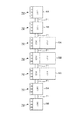
続いて、処理装置群40について説明する。図2は、塗布装置4A、4B、露光、加熱装置5A、5B、5C、現像装置6A、6Bの配置のレイアウトを示している。この図に示すように、塗布装置4A、4B、露光、加熱装置5A、5B、5C、現像装置6A、6Bが、この順に一列に並んでいる。そして各装置間はキャリアCの専用搬送路71により接続されている。
Next, the
図3では、説明を容易にするために図2の処理装置群40の構成を簡略化し、塗布装置4A、露光、加熱装置5A及び現像装置6Bのみ示している。各処理装置は、キャリアCを搬入するためのキャリアステーション72を備えている。キャリアステーション72はロードポート73を備えており、前記専用搬送路71により隣り合う処理装置間のロードポート73、73が接続されている。図4はそのように互いに接続された2基のロードポート73、73の正面を示している。ロードポート73には搬入出ステージをなすキャリア載置部74が設けられており、キャリア載置部74は、キャリアCを保持する保持機構を備えている。キャリア載置部74は、キャリアCの受け渡しを行う後退位置と、キャリアステーション72内にキャリアCからウエハWを払い出す前進位置との間で進退する。
In FIG. 3, for ease of explanation, the configuration of the
前記キャリアCの準備時間は、キャリア載置部74が後退位置でキャリアCを受け取ってから前進位置に移動して装置にウエハWの払い出しを行うまでの時間であり、この準備時間にキャリア載置部74の保持機構によるキャリアCの保持、キャリアCの蓋の開放及びキャリア載置部74によるキャリアCの高さ位置の調整が行われる。前記キャリアCの排出時間は、キャリアCにすべてのウエハWが戻されてから、後退位置に移動するまでの時間であり、この間にキャリアCの蓋の閉鎖及び前記保持機構によるキャリアCの保持の解除が行われる。
The preparation time of the carrier C is a time from when the
キャリア載置部74の上方側には、棚部75、76が設けられており、これら棚部75、76は処理装置に搬入されたキャリアCを一時的に退避させるキャリア待機部をなす退避領域70を備えている。処理装置に搬送されたキャリアCは、キャリア載置部74が塞がっている場合、キャリア載置部74が空くまでキャリアCは退避領域70に退避される。そして、処理装置に搬送された順にキャリアCは退避領域70からキャリア載置部74に搬送される。また、塗布装置4Aを除く処理装置において、棚部76の塗布装置4A側は、当該塗布装置4A側に隣接する処理装置からキャリアCを受け取るための搬入ポート77として構成されている。
塗布装置4Aを除く各処理装置において、各処理装置の棚部76の塗布装置4A側は、当該塗布装置4A側に隣接する処理装置からキャリアCを受け取るための搬入ポート77として構成されている。また、図3に示すように塗布装置4Aには搬入ポート77の代わりに、天井搬送装置12からキャリアCを受け取るための共用搬入ポート78が設けられている。
In each processing apparatus excluding the
現像装置6Bを除く各処理装置において、各処理装置の棚部76の現像装置6B側には、当該現像装置6B側に隣接する処理装置へキャリアCを受け渡すためのキャリア移載機をなす装置間キャリア搬送手段81が設けられている。また、現像装置6Bの棚部76においては、図3に示すように装置間キャリア搬送手段81の代わりに天井搬送装置12へキャリアCを受け渡すための共用搬出ポート79が設けられている。
In each processing apparatus excluding the developing
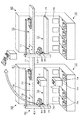
さらにロードポート73は装置内キャリア搬送手段82を備えている。このキャリア搬送手段82は、昇降軸83に沿って昇降自在な基部84とその基部84に接続され、当該基部84に対して鉛直軸まわりに回転自在な多関節の搬送アーム85とを備えている。この昇降軸83は、ガイドレール86に沿って横方向に移動自在に構成されている。キャリア搬送手段82により、棚部75、76の退避領域70、装置間キャリア搬送手段81及びキャリア載置部74間でキャリアCの受け渡しが行われる。図4中矢印の先には、このように受け渡しを行うために搬送アーム85がキャリアCを把持した状態を示している。
Furthermore, the
天井搬送装置12について説明する。天井搬送装置12は、図3に点線で示すレール14と搬送装置本体15とを備え、レール14に沿って搬送装置本体15が移動する。図示を省略しているが搬送装置本体15は、キャリアCを把持する把持部を備え、上流側装置から塗布装置4Aの共用搬入ポート78にキャリアCを搬送すると共に、現像装置6Bに設けられる共用搬出ポート79からキャリアCを搬出する。
The
続いて、塗布装置4Aについて図5を参照しながら説明する。塗布装置4Aに設けられたキャリアステーション72には、処理ステーション101が接続されている。キャリアステーション72内に設けられる搬送アーム102は、キャリア載置台74に載置されたキャリアCと、処理ステーション101に設けられた受け渡しモジュール103との間でウエハWを受け渡す。処理ステーション101では、受け渡しモジュール103と複数段に積層された塗布モジュール104と、複数段に積層された加熱モジュール105とが周方向に設けられている。また、これらのモジュールに囲まれるようにメイン搬送アーム106が設けられる。メイン搬送アーム106は、昇降、回動及び進退自在に構成され、各モジュール間でウエハWを受け渡す。塗布モジュール104は、ウエハWに薬液としてレジストを供給し、レジスト膜を形成する。塗布装置4Bは、塗布装置4Aと同様に構成されているため、詳細な説明を省略する。
Next, the
現像装置6A、6Bは、塗布モジュール104に対応する現像モジュール107を備えており、この現像モジュール107では、ウエハWにレジストの代わりに現像液が供給される。また、塗布装置4の加熱モジュール105に対応する加熱モジュール108が設けられている。これらの違いを除いて現像装置6A、6Bは、塗布装置4Aと同様に構成されている。
The developing devices 6 </ b> A and 6 </ b> B include a developing
続いて、露光、加熱装置5Aについて図6を参照しながら説明する。露光、加熱装置5Aが備えるキャリアステーション72には処理ステーション111が接続されており、キャリアステーション72内に設けられる搬送アーム102は、キャリア載置台74に載置されたキャリアCと処理ステーション111に設けられた受け渡しモジュール113との間でウエハWを受け渡す。処理ステーション111では、受け渡しモジュール113と、複数段に積層された加熱モジュール114と、受け渡しモジュール115とが周方向に設けられ、これらのモジュールに囲まれるようにメイン搬送アーム116が設けられる。
Next, the exposure and
メイン搬送アーム116は、昇降、回動、進退自在に構成され、各モジュール間でウエハWを受け渡す。処理ステーション111には、インターフェイスブロック117を介して露光装置118に接続されている。インターフェイスアーム119は、受け渡しモジュール115と、露光装置118との間でウエハWを受け渡す。露光、加熱装置5B、5Cは、露光、加熱装置5Aと同様に構成されている。
The
処理装置群40の各処理装置間でのキャリアCの受け渡しについて図7を参照しながら説明する。前記装置間キャリア搬送手段81は多関節のアームとして構成され、装置内キャリア搬送手段82によりアームの先端部にキャリアCが受け渡されると、この先端部はキャリアCを保持した状態で、現像装置6側に隣接する処理装置の搬入ポート77に向けて移動する。搬入ポート77は、例えば昇降自在な支持ピン81aを備え、支持ピン81aと装置間キャリア搬送手段81との協働作業により前記搬入ポート77にキャリアCが受け渡される。
The delivery of the carrier C between the processing devices of the
キャリア搬送手段81、82及び搬入ポート77の電源やコントローラは、これら搬送手段及びポートが設けられる処理装置の電源やコントローラから分離されている。これにより、キャリアCが搬送される経路の処理装置で電源が落ちたり、メンテナンスが行われたり、突然に処理が停止しても、この処理装置で処理を行わないロットを含むキャリアCは、次の工程を行う処理装置に搬送されるようになっている。
The power supplies and controllers of the carrier transfer means 81 and 82 and the carry-in
続いて、基板処理システム1の作用について図8のフローを参照しながら説明する。この例では塗布装置4におけるロットの処理終了から露光加熱装置における前記ロットの処理開始までの経過時間が制御される。ホストコンピュータ10が、上流側装置からキャリアCのロットの処理が終了したことを示す信号を受信する(ステップS1)。ホストコンピュータ10が天井搬送装置12に信号を送信し、天井搬送装置12は上流側装置でキャリアCを受け取り、共用搬入ポート78にキャリアCを搬入する(ステップS2)。
Next, the operation of the
ホストコンピュータ10が、クラスタコントローラ21に前記キャリアC内のロットのID、レシピ、当該レシピに対応する処理パラメータ及びウエハWの枚数などの付帯情報を送信し、これらのデータが、クラスタコントローラ21のメインメモリ25に格納される(ステップS3)。
The
そして、クラスタコントローラ21は、より早く前記ロットの処理を開始できる塗布装置4を選択する。この塗布装置4の選択について、一例として図9のタイムチャートを参照しながら説明する。共用搬入ポート78に前記キャリアCが搬入された時刻t0において、例えば塗布装置4AにはロットA、Bが既に搬入されており、塗布装置4BにはロットC、Dが既に搬入されているものとし、今回新たに基板処理システム1に搬入されるロットはロットEとする。また、塗布装置4A、4BではロットA、Bが処理中であるものとする。
Then, the
クラスタコントローラ21は、ロットA、Bのキャリアの処理が終了するまでの時間、各ロット処理間でモジュールの整定に要する時間、ロットC、Dのキャリアの処理時間に基づいて、ロットC、Dのキャリアの処理が終了する時刻t1、t2を夫々演算する。続いて、クラスタコントローラ21は、ロットEについてウエハWの枚数やレシピ、処理パラメータなどのデータを塗布装置4A、4Bに送信する。塗布装置4A、4Bは、送信されたデータに基づきロットEのキャリアの処理時間を演算すると共にモジュールの整定に要する時間を演算する。クラスタコントローラ21は、演算されたこれらの情報を受信して、塗布装置4A、4Bで夫々ロットEを処理するとした場合におけるロットEのキャリアの処理終了時刻t3、t4を演算する。ここでは前記整定の開始時刻は、ロットC、Dのキャリアの処理が終了する時刻t1、t2であるものとする。
Based on the time until the processing of the carriers of the lots A and B, the time required for setting the module between the lot processing, and the processing time of the carriers of the lots C and D, the
続いて、クラスタコントローラ21は、時刻t1−t3間、時刻t2−t4間が夫々装置でメンテナンスを行う時間と重なっていないかどうかを判定する。重なっていなければ、時刻t1、t2後に前記整定が終わる時刻t5、t6をロットEの処理開始時刻とする。時刻t1−t3間、時刻t2−t4間が夫々装置でメンテナンスを行う時間に重なっている場合、例えば当該メンテナンス終了時から前記整定を行うものとして、改めてロットEのキャリアの処理開始時刻t5、t6を演算する。図9の例では時刻t1−t3間が、塗布装置4Aでメンテナンスを行う時間に重なっている。そこで、図中矢印で示すように、メンテナンス終了後に、前記整定、ロットEのキャリアの処理が順次行われるように、これら整定及びキャリアの処理時間をずらして前記処理開始時刻t5が演算されている。
Subsequently, the
そして、クラスタコントローラ21は、塗布装置4AでのロットEのキャリアの処理開始時刻t5と、塗布装置4BでのロットEのキャリアの処理開始時刻t6とのうちどちらが早い時刻か判定し、時刻が早いほうの塗布装置4にロットEを含むキャリアCを搬送するように決定する。
Then, the
このようにクラスタコントローラ21は、塗布装置4A、4Bにおいて、先に塗布装置4A、4Bで処理されることが決まっているロットの処理状況に基づいて、各塗布装置で夫々ロットEを処理するために整定を行うことが可能になる時刻を検出する。そして、各塗布装置において、当該ロットEの整定時間及びロットEの処理時間がメンテナンス時間と重なるか否か判定する。重なる場合は、メンテナンス終了時刻に整定を行う時刻をずらし、各装置4A、4BでロットEの処理が可能になる時刻を検出して、その時刻に基づきロットEの搬送先を決定する。
In this way, the
塗布装置4の決定方法について説明したが、クラスタコントローラ21は、露光、加熱装置5及び現像装置6についても、塗布装置4と同様に各処理装置における処理状況、メンテナンス情報及び整定時間に基づいて、ロットEのキャリアCの処理開始時刻を決定する。そして、露光、加熱装置5A〜5Cのうち、処理開始時刻が最も早い装置にロットEのキャリアCを搬送するように決定する。また、現像装置6A〜6Bのうち、処理開始時刻が最も早い装置にロットEのキャリアを搬送するように決定する(ステップS4)。つまり、最も早くロットEの処理を終了できるように、処理装置の選択が行われる。
Although the determination method of the coating device 4 has been described, the
クラスタコントローラ21は、ステップS4で選択した各処理装置に送信したロットEの処理パラメータで処理を行うように指示を出す。そして、共用搬入ポート77からキャリア搬送手段81及び82を介して選択した塗布装置4(図9の場合は塗布装置4B)のキャリア載置台74または退避領域70にキャリアCを搬送する(ステップS5)。退避領域70にキャリアCを搬送した場合は、キャリア載置台74が空き次第、当該載置台74にキャリアCが搬送される。
The
続いて、クラスタコントローラ21は、選択した塗布装置4におけるロットEのキャリアの処理終了時刻(図9の例では時刻t4がロットEの処理終了時刻である)と、選択した露光、加熱装置5のロットEの処理開始時刻との差分を演算し、塗布処理終了から露光処理開始までの予測経過時間Ta1を演算する(ステップS6)。
Subsequently, the
続いて、クラスタコントローラ21は、前記予測経過時間Ta1が予め設定された時間Ta0以内であるか否かを判定する(ステップS7)。ステップS7で予測経過時間Ta1が設定時間Ta0以内であると判定した場合は、選択した塗布装置4で、ロットEの手前のロット(図9ではロットD)のキャリアの処理、ロットEを処理するためのモジュールの整定が順次終わり、ロットEのキャリアが処理可能になった時点で、当該キャリアの処理を開始する(ステップS8)。ステップS7で予測待ち時間Taが設定時間T0以内では無いと判定した場合は、ロットEが処理可能になった時点から(Ta1−Ta0)経過後にロットEの処理を開始する(ステップS9)。
Subsequently, the
以降、ウエハWの搬送経路を示した図10も参照しながら説明する。キャリアCから払い出されたウエハWは、塗布装置4を受け渡しモジュール103→塗布モジュール104の順で搬送され、塗布モジュール104でウエハWにレジストが塗布される。続いてウエハWは、加熱モジュール105で加熱処理を受け、受け渡しモジュール103→キャリアCの順番で搬送される。
Hereinafter, description will be made with reference to FIG. 10 showing the transfer path of the wafer W. The wafer W delivered from the carrier C is transferred in the order of the
塗布装置4でキャリアC内のすべてのウエハWについて処理が終了すると、キャリアCは搬送手段81、82により選択された露光、加熱装置5のキャリア載置部74へ前記キャリアCを搬送する。露光、加熱装置5でウエハWの処理が可能になると、キャリアCからウエハWが順次払い出される。前記ウエハWは、受け渡しモジュール113→受け渡しモジュール115→露光装置118の順で搬送され、露光処理をうける。露光処理を受けたウエハWは、受け渡しモジュール115→加熱モジュール114の順で搬送され、加熱モジュール114で加熱処理(ポストエクスポージャベーク)を行う。加熱処理を受けたウエハWは、受け渡しモジュール113を経由してキャリアCに戻される。
When the processing is completed for all the wafers W in the carrier C by the coating apparatus 4, the carrier C transports the carrier C to the
続いて、キャリアCは選択された現像装置6に搬送される。そして、キャリアCから払い出されたウエハWは、現像装置6の受け渡しモジュール103→現像モジュール107の順で搬送され、現像が供給される。続いてウエハWは、加熱モジュール108で加熱処理(ポストベーク)を受け、受け渡しモジュール103→キャリアCの順番で搬送される(ステップS10)。
Subsequently, the carrier C is conveyed to the selected developing device 6. Then, the wafer W delivered from the carrier C is transported in the order of the
すべてのロットEのウエハWがキャリアCに搬送された後、キャリアCは共用搬出ポート79に搬送され(ステップS11)、クラスタコントローラ21はキャリアCの搬出準備ができた旨を示す信号をホストコンピュータ10に出力する。ホストコンピュータ10が天井搬送装置12に信号を送信し、天井搬送装置12が共用搬出ポート79でキャリアCを受け取り、下流側の装置へ当該キャリアCを搬送する(ステップS12)。
After the wafers W of all the lots E are transferred to the carrier C, the carrier C is transferred to the common transfer port 79 (step S11), and the
この基板処理システム1によれば、クラスタコントローラ21が、処理装置のロットの処理状況及びメンテナンス状況に基づいて、同種の処理装置の中でロットの処理の開始時点が早い装置を選択する。これによって、例えば塗布、現像装置に露光装置を接続した基板処理システムに比べて、ロットの搬送先を上述のように処理装置の状況に応じて選択できるので、各処理装置で効率よくロットの処理を行うことができ、スループットの向上を図ることができる。さらに、選択した塗布装置4での処理終了時刻から露光処理開始時刻までの予測経過時間Ta1を計算し、その予測経過時間に基づいてウエハWの払い出しが制御される。従って、ウエハWにレジスト塗布後、露光するまでの時間が長くなることが抑えられるので、ウエハWへ無駄に処理を行うことを防ぐことができ、コストの低下を図ることができる。
According to this
この基板処理システム1においては、天井搬送装置12が、1つのキャリアCに対して共用搬入ポート78に搬入するとき及び共用搬出ポート79から搬出するときの2回のみアクセスする。そして、各処理装置間でキャリアCは、基板処理システム1の専用の装置間キャリア搬送手段81により受け渡される。従って、天井搬送装置12が処理装置ごとにウエハWの搬入出を行う場合よりも、天井搬送装置12の負荷が軽くなるし、天井搬送装置1の動作状況によらず、処理装置間でキャリアCを搬送できるため、スループットの向上を図ることができる。
In this
続いて、第1の実施形態の第1の変形例のフローを図10に示す。この変形例ではレジスト塗布処理終了後から露光処理開始までの予測経過時間が制御される代わりに、露光、加熱処理終了後から現像処理開始までの予測経過時間が制御される。先ず、既述のステップS1〜S5に従って処理が行われる。そして、クラスタコントローラ21は、第1の実施形態と同様に、各処理装置における処理状況、メンテナンス情報及び整定時間に基づいて、任意のロットのキャリアCの露光、加熱装置の処理終了時点と、現像処理開始時点とを演算する。さらに前記露光加熱処理終了時点から現像処理開始時点までの予測経過時間Tb1を演算する(ステップS101)。続いて、クラスタコントローラ21は、演算した予測経過時間Tb1が、予め設定された時間Tb0以内であるか否かを判定する(ステップS102)。
Subsequently, FIG. 10 shows a flow of a first modification of the first embodiment. In this modification, instead of controlling the estimated elapsed time from the end of the resist coating process to the start of the exposure process, the estimated elapsed time from the end of the exposure and heating processes to the start of the development process is controlled. First, processing is performed according to steps S1 to S5 described above. Then, as in the first embodiment, the
ステップS102で予測経過時間Tb1が設定時間Tb0以内であると判定した場合は、前記キャリアCが処理可能になった時点で、選択した塗布装置4でロットの処理を開始する(ステップS103)。ステップS103で予測経過時間Tb1が設定時間Tb0以内では無いと判定した場合は、前記キャリアCが処理可能になった時点から(Tb1−Tb0)経過後にロットEの処理を開始する(ステップS104)。その後は、既述のステップS10〜S12に従って処理が進行する。 If it is determined in step S102 that the estimated elapsed time Tb1 is within the set time Tb0, the lot application process is started by the selected coating apparatus 4 when the carrier C becomes processable (step S103). If it is determined in step S103 that the predicted elapsed time Tb1 is not within the set time Tb0, the processing of the lot E is started after the time (Tb1-Tb0) has elapsed since the carrier C can be processed (step S104). Thereafter, the process proceeds according to steps S10 to S12 described above.
第1の実施形態の第2の変形例のフローを図12に示す。この第2の変形例では、レジスト塗布処理終了後から露光処理開始までの予測経過時間及び露光、加熱処理終了後から現像処理開始までの予測経過時間の両方が制御される。先ず、既述のステップS1〜S5に従って処理が行われ、その後クラスタコントローラ21は、第1の実施形態のステップS6と同様に、各処理装置における処理状況、メンテナンス情報及び整定時間に基づいて、任意のロットのキャリアCにおける塗布装置での処理終了時点から露光開始時点までの予測経過時間Ta1を計算する。また、クラスタコントローラ21は、第1の変形例のステップS101と同様に、露光加熱処理終了時点から現像処理開始時点までの予測経過時間Tb1を演算する(ステップS201)。
FIG. 12 shows a flow of a second modification of the first embodiment. In the second modification, both the estimated elapsed time from the end of the resist coating process to the start of the exposure process and the estimated elapsed time from the end of exposure and the heating process to the start of the development process are controlled. First, processing is performed in accordance with the above-described steps S1 to S5, and thereafter, the
続いて、クラスタコントローラ21は、演算した予測経過時間Ta1が、予め設定された時間Ta0以内であるか否かを判定する。さらに、予測経過時間Tb1が、予め設定された時間Tb0以内であるか否かを判定する(ステップS202)。
Subsequently, the
予測経過時間Ta1が設定時間Ta0以内であり、且つ予測経過時間Tb1が設定時間Tb0以内であると判定したときは、選択した塗布装置4で前記ロットが処理可能になった時点で、当該ロットの処理を開始する(ステップS203)。 When it is determined that the predicted elapsed time Ta1 is within the set time Ta0 and the predicted elapsed time Tb1 is within the set time Tb0, when the lot can be processed by the selected coating apparatus 4, the lot Processing is started (step S203).
予測経過時間Ta1が設定時間Ta0を超えているか、または予測経過時間Tb1が設定時間Tb1を超えている場合、クラスタコントローラ21は、その超えている時間を演算する。そして、選択した塗布装置4で前記ロットが処理可能になった時点から、演算した時間が経過したときに当該ロットの処理を開始する(ステップS204)。
If the predicted elapsed time Ta1 exceeds the set time Ta0 or the predicted elapsed time Tb1 exceeds the set time Tb1, the
予測経過時間Ta1が設定時間Ta0を超えており、且つ予測経過時間Tb1が設定時間Tb1を超えている場合、クラスタコントローラ21は、各予測経過時間Ta1、Tb1について夫々超えている時間を演算する。そして、選択した塗布装置4で、前記ロットが処理可能になった時点から、超えている時間が長い方の時間が経過したときに当該ロットの処理を開始する(ステップS204)。その後は、既述のステップS10〜S12に従って処理が進行する。
When the predicted elapsed time Ta1 exceeds the set time Ta0 and the predicted elapsed time Tb1 exceeds the set time Tb1, the
基板処理システム1において、ロットについて、上記のようにどの工程の処理を終了してから、どの工程の処理を開始するまでの時間を制御するかは、例えばユーザが任意に選択できるようになっている。
In the
(第2の実施形態)
図13には第2の実施形態の基板処理システム121のレイアウトを示している。塗布装置4A、4B、露光、加熱装置5A、5B、現像装置6A、6B、検査装置7A、7Bが、この順に接続されている。
(Second Embodiment)
FIG. 13 shows a layout of the substrate processing system 121 of the second embodiment.
検査装置7A、7Bは、現像後のウエハWの表面状態を検査する検査モジュールを備えており、検査装置7A、7Bは、処理ステーション101に塗布モジュールの代わりに前記検査モジュールが搭載されていることを除けば、塗布装置4Aと同様に構成されている。現像後のウエハWは、検査装置7Aまたは7Bで検査される。キャリアCは、塗布装置4A側から検査装置7B側へ向かって搬送され、検査装置7Bのキャリアステーション72には共用搬出ポート79が設けられている。
The inspection apparatuses 7A and 7B include an inspection module that inspects the surface state of the wafer W after development. The inspection apparatuses 7A and 7B include the inspection module mounted on the
この基板処理システム121においては、基板処理システム1と同様に各装置からメンテナンス情報とウエハWの処理状況とレシピに基づいて決定される整定時間とがクラスタコントローラ21に送信され、クラスタコントローラ21はこれらに基づいて、ロットの搬送先を決定する。塗布装置4、露光、加熱装置5、現像装置6の他に検査装置についても7A、7Bのどちらにロットを搬送するか、処理開始時刻の早いほうに決定する。その後は、第1の実施形態と同様に塗布装置4へのロットの払い出しが制御される。
In this substrate processing system 121, as in the
この基板処理システム121においては、第1の実施形態の各例と同様に、検査装置の処理開始時点と、その上流側の処理装置の処理終了時点との間の予測経過時間を演算し、その予測経過時間に応じて塗布装置にウエハWを払い出すように制御することができる。 In this substrate processing system 121, as in each example of the first embodiment, the estimated elapsed time between the processing start time of the inspection apparatus and the processing end time of the upstream processing apparatus is calculated, Control can be performed so that the wafer W is dispensed to the coating apparatus according to the predicted elapsed time.
検査装置7A、7Bの代わりに現像処理後のウエハWに洗浄処理を行う複数の洗浄装置を設けてもよい。洗浄装置は、検査モジュールの代わりに、ウエハWに洗浄液を供給して洗浄を行う洗浄モジュールを備える他は検査装置7A、7Bと同様の構成である。洗浄装置は、検査モジュール7A,7Bの前段に設けてもよいし、検査モジュール7A,7Bの後段に設けてもよい。
Instead of the
クラスタコントローラ21及びホストコンピュータ10の接続としては図1の例に限られるものではなく、図14のように接続してもよい。この例ではクラスタコントローラ21がホストコンピュータ10の下流に処理装置群40と並列に接続されている。この例ではホストコンピュータ10からロットのID、ロットのレシピ及び処理パラメータがクラスタコントローラ21及び処理装置群へ送信される。クラスタコントローラ21が故障した場合には、上記のような処理装置40の選択、予測経過時間に基づいたロットの払い出し制御はできなくなるが、処理装置群40が個別に動作し、処理装置間でウエハWを搬送し、処理を行うことができる。
The connection between the
上記の各例では装置間キャリア搬送機構81を設けているが、このようなキャリア搬送機構を設ける代わりに天井搬送装置12を用いて各装置間でキャリアCを搬送することができる。例えば各処理装置にキャリア搬送機構81の代わりに搬出ポートを設け、処理装置で処理を終えたキャリアCを当該搬出ポートに搬送する。そして、天井搬送装置12が前記搬出ポートからキャリアCを受け取り、選択された後段の処理装置の搬入ポート77に当該キャリアCを載置するようにしてもよい。
In each of the above examples, the inter-device
例えば、各実施形態において、クラスタコントローラ21は、各処理装置のメンテナンス時間に関わらず、ロットの処理状況及び整定時間に基づいて、ロットの搬送先の処理装置を決定し、さらにキャリアCからウエハWの払い出しを制御してもよい。以下、そのような一例について説明する。この例では第1の実施形態と同様に塗布装置4での処理後から露光、加熱装置5の処理開始までの時間が制御されているものとする。
For example, in each embodiment, the
第1の実施形態の図9のようにロットA〜ロットDの処理時間及び各ロットC〜ロットEを処理するための整定時間が設定されているとした場合、メンテナンス時間を考慮しなければ、ロットEが処理可能になる時刻は塗布装置4Aの方が早いため、クラスタコントローラ21は、当該塗布装置4AにロットEのキャリアを搬送するように決定する。そして、上記のステップS5〜S6に従って、ロットEのキャリアが塗布装置4Aに搬送され、予測経過時間Ta1が演算される。
As shown in FIG. 9 of the first embodiment, when the processing time for lot A to lot D and the settling time for processing each lot C to lot E are set, if the maintenance time is not considered, Since the time when the lot E can be processed is earlier in the
ここで、各塗布装置4では、例えばロットの整定時間及び処理時間にメンテナンス時間が重なると、メンテナンスの開始時刻を当該ロットの処理終了時刻にずらすように変更するように構成されているものとする。具体的に、前記ロットEについて見ると図15(a)に示すように、塗布装置4Aのメンテナンス時間が当該ロットEの整定時間及び処理時間に重なっているので、塗布装置4Aは、図15(b)に示すようにロットEの処理が終了する時刻t3からメンテナンスが開始されるようにメンテナンス時間の設定を変更する。ロットEについては、これ以降、既述のS7以降のステップに従って処理が行われる。
Here, each coating apparatus 4 is configured to change the maintenance start time to shift to the lot processing end time when the maintenance time overlaps with the settling time and processing time of the lot, for example. . Specifically, when looking at the lot E, as shown in FIG. 15A, the maintenance time of the
この設定変更により発生する塗布装置4Aに搬入される後続のロット(図15ではロットFとしている)の処理開始時刻の変更についての情報が、塗布装置4Aからクラスタコントローラ21に送信される。クラスタコントローラ21はこのように更新された塗布装置4Aの処理状況に基づいて、搬送先が未決定の後続のロットについて、ロットEと同様に搬送先を決定し、処理を行う。このような実施形態においても、上記の各実施形態と同様の効果があるが、第1の実施形態のようにクラスタコントローラ21が、メンテナンス時間も参照して処理装置の選定及び予測経過時間Ta1の演算が行われることで、より確実にウエハWの払い出し時刻を管理することができ、ウエハWに無駄な処理を行うことを抑えることができる。
Information about a change in the processing start time of the subsequent lot (referred to as lot F in FIG. 15) carried into the
1 基板処理システム
10 ホストコンピュータ
11 自動搬送制御部
12 天井搬送装置
21 クラスタコントローラ
25 メインメモリ
31 選択プログラム
32 払い出し制御プログラム
33 キャリア搬送制御プログラム
40 処理装置群
4A、4B 塗布装置
5A、5B、5C 露光、加熱装置
6A、6B 現像装置
71 専用搬送路
72 キャリアステーション
81 装置間キャリア搬送手段
82 装置内キャリア搬送手段
DESCRIPTION OF
Claims (10)
(1) 基板に対してレジスト膜を形成するための複数の塗布装置と、基板上のレジスト膜を露光するための複数の露光装置と、露光後の基板を現像液により現像するための複数の現像装置と、を含む処理装置群を備えたこと、
(2) 前記塗布装置、露光装置及び現像装置の各々は、キャリアが搬入出される搬入出ステージと、キャリアを待機させるためのキャリア待機部と、前記搬入出ステージとキャリア待機部との間でキャリアを移載するキャリア移載機と、前記搬入出ステージに載置されたキャリアに対して基板の受け渡しを行う受け渡し機構と、この受け渡し機構により受け渡された基板に対して目的とする処理を行う処理部と、を含むこと、
(3) 処理装置群に対して共通化され、自動搬送装置からキャリアを受け取るための搬入ポート、及び処理装置群に対して共通化され、自動搬送装置にキャリアを受け渡すための搬出ポートを設けたこと、
(4) 互いに隣接する処理装置の間をキャリアを搬送する専用の搬送機構を設けたこと、
(5) 前記処理装置群に対して管理を行うと共に前記キャリア移載機及び前記専用の搬送機構を制御するグループコントローラを設けたこと、
(6) 前記自動搬送装置により運ばれるキャリア内の基板について処理レシピをグループコントローラに対して送信するホストコンピュータを設けたこと、
からなり、
(7) 前記グループコントローラは、
(7−1) 前記搬入ポートに搬入されたキャリア内の基板に対し順次複数の処理装置により処理を行ったときに最終の処理装置にて処理が終了する時点が最も早い処理装置の組み合わせを、基板の処理レシピ及び各処理装置における処理状況に基づいて決定するステップ
(7−2) 決定された処理装置の組み合わせにおいて、予め決めた一の処理装置によるロットの処理終了時点から当該ロットについて、予め決めた下流側の処理装置による処理開始時点までの予測経過時間を、基板の処理レシピ及び各処理装置における処理状況に基づいて計算し、予測経過時間が設定時間を越えているときには、予測経過時間が設定時間内に収まるように前記一の処理装置または当該一の処理装置よりも上流側の処理装置に基板を払い出すタイミングを決定するステップ
(7−3) 前記複数の処理装置による一連の処理が終了した基板を収納したキャリアを搬出ポートに搬出するステップ
を実行するためのプログラムを備えていることを特徴とする基板処理システム。 In a substrate processing system that takes out a substrate from a carrier that stores substrates for each lot and performs processing,
(1) A plurality of coating devices for forming a resist film on a substrate, a plurality of exposure devices for exposing a resist film on the substrate, and a plurality of devices for developing the exposed substrate with a developer. A processing device group including a developing device;
(2) Each of the coating device, the exposure device, and the developing device includes a carrier loading / unloading stage in which a carrier is loaded / unloaded, a carrier standby unit for waiting the carrier, and a carrier between the loading / unloading stage and the carrier standby unit. A carrier transfer machine, a delivery mechanism for delivering the substrate to the carrier placed on the carry-in / out stage, and a target process for the substrate delivered by the delivery mechanism Including a processing unit,
(3) A common loading port for receiving a carrier from the automatic transfer device and a common carry-out port for delivering the carrier to the automatic conveying device are provided for the processing device group. Was it,
(4) Providing a dedicated transport mechanism for transporting carriers between processing devices adjacent to each other;
(5) Provided with a group controller for controlling the processing device group and controlling the carrier transfer machine and the dedicated transport mechanism;
(6) A host computer is provided for transmitting a processing recipe to the group controller for the substrate in the carrier carried by the automatic transfer device,
Consists of
(7) The group controller
(7-1) A combination of processing devices having the earliest point in time when processing is completed in the final processing device when a plurality of processing devices sequentially process the substrate in the carrier carried into the carry-in port. Step of determining based on substrate processing recipe and processing status in each processing apparatus (7-2) In the determined combination of processing apparatuses, the lot is processed in advance from the time when the processing of the lot by one predetermined processing apparatus is completed. The estimated elapsed time until the processing start time by the determined downstream processing apparatus is calculated based on the processing recipe of the substrate and the processing status in each processing apparatus, and when the estimated elapsed time exceeds the set time, the estimated elapsed time Is a timing at which the substrate is dispensed to the one processing apparatus or a processing apparatus upstream of the one processing apparatus so as to be within a set time. (7-3) A substrate processing system comprising: a program for executing a step of unloading a carrier containing a substrate for which a series of processing by the plurality of processing apparatuses has been completed to an unloading port .
(1) 基板に対してレジスト膜を形成するための複数の塗布装置と、基板上のレジスト膜を露光するための複数の露光装置と、露光後の基板を現像液により現像するための複数の現像装置と、を含む処理装置群を備えたこと、
(2) 前記塗布装置、露光装置及び現像装置の各々は、キャリアが搬入出される搬入出ステージと、キャリアを待機させるためのキャリア待機部と、前記搬入出ステージとキャリア待機部との間でキャリアを移載するキャリア移載機と、前記搬入出ステージに載置されたキャリアに対して基板の受け渡しを行う受け渡し機構と、この受け渡し機構により受け渡された基板に対して目的とする処理を行う処理部と、を含むこと、
(3) 前記処理装置群に対して管理を行うと共に前記キャリア移載機を制御するグループコントローラを設けたこと、
(4) 前記各搬入出ステージへ前記キャリアを搬送するための自動搬送装置により運ばれる当該キャリア内の基板について処理レシピをグループコントローラに対して送信するホストコンピュータを設けたこと、
からなり、
(5) 前記グループコントローラは、
(5−1) 前記自動搬送装置により搬送されるキャリア内の基板に対し順次複数の処理装置により処理を行ったときに最終の処理装置にて処理が終了する時点が最も早い処理装置の組み合わせを、基板の処理レシピ及び各処理装置における処理状況に基づいて決定するステップ
(5−2) 決定された処理装置の組み合わせにおいて、自動搬送装置により最初の処理装置のキャリア待機部にキャリアを搬入するステップ
(5−3) 自動搬送装置により、上流側の処理装置のキャリア待機部から下流側の処理装置のキャリア待機部に順次キャリアを搬送するステップ
(5−4) 決定された処理装置の組み合わせにおいて、予め決めた一の処理装置によるロットの処理終了時点から当該ロットについて、予め決めた下流側の処理装置による処理開始時点までの予測経過時間を、基板の処理レシピ及び各処理装置における処理状況に基づいて計算し、予測経過時間が設定時間を越えているときには、予測経過時間が設定時間内に収まるように前記一の処理装置または当該一の処理装置よりも上流側の処理装置に基板を払い出すタイミングを決定するステップ
(5−5) 一連の処理を終了した基板を収納したキャリアを、最終処理を行った処理装置のキャリア待機部から自動搬送装置により搬出するステップ
を実行するためのプログラムを備えていることを特徴とする基板処理システム。 In a substrate processing system that takes out a substrate from a carrier that stores substrates for each lot and performs processing,
(1) A plurality of coating devices for forming a resist film on a substrate, a plurality of exposure devices for exposing a resist film on the substrate, and a plurality of devices for developing the exposed substrate with a developer. A processing device group including a developing device;
(2) Each of the coating device, the exposure device, and the developing device includes a carrier loading / unloading stage in which a carrier is loaded / unloaded, a carrier standby unit for waiting the carrier, and a carrier between the loading / unloading stage and the carrier standby unit. A carrier transfer machine, a delivery mechanism for delivering the substrate to the carrier placed on the carry-in / out stage, and a target process for the substrate delivered by the delivery mechanism Including a processing unit,
(3) providing a group controller for managing the processing device group and controlling the carrier transfer machine ;
(4) A host computer is provided that transmits a processing recipe to a group controller for a substrate in the carrier that is carried by an automatic carrying device for carrying the carrier to each carry-in / out stage .
Consists of
(5) The group controller
(5-1) A combination of processing devices having the earliest point at which processing is completed in the final processing device when a plurality of processing devices sequentially process the substrate in the carrier transported by the automatic transport device. Step of determining based on substrate processing recipe and processing status in each processing apparatus (5-2) Step of carrying carrier into carrier waiting section of first processing apparatus by automatic transfer device in determined combination of processing apparatuses (5-3) Step of sequentially transferring carriers from the carrier standby unit of the upstream processing device to the carrier standby unit of the downstream processing device by the automatic transfer device. (5-4) In the determined combination of processing devices, Processing by a predetermined downstream processing device for the lot from the end of processing of the lot by one predetermined processing device The estimated elapsed time up to the start time is calculated based on the processing recipe of the substrate and the processing status in each processing apparatus, and when the estimated elapsed time exceeds the set time, the estimated elapsed time falls within the set time. Step for determining timing for delivering a substrate to one processing device or a processing device upstream of the one processing device (5-5) A carrier storing a substrate for which a series of processing has been completed is subjected to final processing A substrate processing system comprising a program for executing a step of unloading from a carrier standby section of a processing apparatus by an automatic transfer apparatus.
前記検査装置は、キャリアが搬入出される搬入出ステージと、キャリアを待機させるためのキャリア待機部と、前記搬入出ステージとキャリア待機部との間でキャリアを移載するキャリア移載機と、前記搬入出ステージに載置されたキャリアに対して基板の受け渡しを行う受け渡し機構と、この受け渡し機構により受け渡された基板に対して検査を行う検査部と、を含むことを特徴とする請求項1ないし3のいずれか一項に記載の基板処理システム。 The processing device group includes a plurality of inspection devices for inspecting a substrate developed by a developing device,
The inspection apparatus includes a loading / unloading stage in which a carrier is loaded / unloaded, a carrier standby unit for waiting a carrier, a carrier transfer machine that transfers a carrier between the loading / unloading stage and the carrier standby unit, 2. A delivery mechanism for delivering a substrate to a carrier placed on a carry-in / out stage, and an inspection unit for inspecting a substrate delivered by the delivery mechanism. The substrate processing system as described in any one of thru | or 3.
前記洗浄装置は、キャリアが搬入出される搬入出ステージと、キャリアを待機させるためのキャリア待機部と、前記搬入出ステージとキャリア待機部との間でキャリアを移載するキャリア移載機と、前記搬入出ステージに載置されたキャリアに対して基板の受け渡しを行う受け渡し機構と、この受け渡し機構により受け渡された基板に対して洗浄を行う洗浄部と、を含むことを特徴とする請求項1ないし4のいずれか一項に記載の基板処理システム。 The processing device group includes a plurality of cleaning devices for cleaning the substrate developed by the developing device,
The cleaning device includes a loading / unloading stage where a carrier is loaded / unloaded, a carrier standby unit for waiting a carrier, a carrier transfer machine for transferring a carrier between the loading / unloading stage and the carrier standby unit, 2. A transfer mechanism for transferring a substrate to a carrier placed on a carry-in / out stage, and a cleaning unit for cleaning the substrate transferred by the transfer mechanism. The substrate processing system as described in any one of thru | or 4.
前記塗布装置、露光装置及び現像装置の各々は、キャリアが搬入出される搬入出ステージと、キャリアを待機させるためのキャリア待機部と、前記搬入出ステージとキャリア待機部との間でキャリアを移載するキャリア移載機と、前記搬入出ステージに載置されたキャリアに対して基板の受け渡しを行う受け渡し機構と、この受け渡し機構により受け渡された基板に対して目的とする処理を行う処理部と、を含む基板処理方法において、
ロット毎に基板を収納したキャリアを自動搬送装置により、処理装置群に対して共通化された搬入ポートに搬入する工程と、
自動搬送装置により運ばれるキャリア内の基板についてホストコンピュータから処理レシピをグループコントローラに対して送信する工程と、
前記搬入ポートに搬入されたキャリア内の基板に対し順次複数の処理装置により処理を行ったときに最終の処理装置にて処理が終了する時点が最も早い処理装置の組み合わせを、基板の処理レシピ及び各処理装置における処理状況に基づいて前記グループコントローラが決定する工程と、
決定された処理装置の組み合わせにおいて、予め決めた一の処理装置によるロットの処理終了時点から当該ロットについて、予め決めた下流側の処理装置による処理開始時点までの予測経過時間を、基板の処理レシピ及び各処理装置における処理状況に基づいて計算する工程と、
予測経過時間が設定時間を越えているときには、予測経過時間が設定時間内に収まるように前記一の処理装置または当該一の処理装置よりも上流側の処理装置に基板を払い出すタイミングを前記グループコントローラが決定する工程と、
上流側の処理装置により処理が終了した基板を収納したキャリアを、互いに隣接する処理装置の間をキャリアを搬送する専用の搬送機を介して下流側の処理装置に搬送する工程と、
前記複数の処理装置による一連の処理が終了した基板を収納したキャリアを、処理装置群に対して共通化された搬出ポートに搬出する工程と、を含むことを特徴とする基板処理方法。 A plurality of coating devices for forming a resist film on the substrate; a plurality of exposure devices for exposing the resist film on the substrate; and a plurality of developing devices for developing the exposed substrate with a developer; And a processing device group including
Each of the coating device, the exposure device, and the developing device transfers a carrier between a carry-in / out stage where the carrier is carried in / out, a carrier standby unit for waiting the carrier, and the carry-in / out stage and the carrier standby unit A carrier transfer machine, a delivery mechanism that delivers a substrate to the carrier placed on the carry-in / out stage, and a processing unit that performs a target process on the substrate delivered by the delivery mechanism; In a substrate processing method including:
A step of loading a carrier storing a substrate for each lot into a loading port shared by a processing device group by an automatic transfer device;
Transmitting a processing recipe from the host computer to the group controller for the substrate in the carrier carried by the automatic transfer device;
When a substrate in the carrier carried into the carry-in port is sequentially processed by a plurality of processing devices, a combination of the processing devices with the earliest timing at which the processing ends in the final processing device, A step of determining the group controller based on a processing status in each processing apparatus;
In the determined combination of processing apparatuses, the estimated elapsed time from the processing end time of a lot by a predetermined processing apparatus to the processing start time by a predetermined downstream processing apparatus for the lot is determined as a substrate processing recipe. And a step of calculating based on the processing status in each processing device,
When the predicted elapsed time exceeds the set time, the timing for dispensing the substrate to the one processing device or a processing device upstream of the one processing device so that the predicted elapsed time is within the set time is the group. The process determined by the controller;
A step of transporting a carrier containing a substrate that has been processed by an upstream processing apparatus to a downstream processing apparatus via a dedicated transporter that transports the carrier between adjacent processing apparatuses;
And a step of unloading a carrier containing a substrate that has been subjected to a series of processes by the plurality of processing apparatuses to an unloading port that is made common to the processing apparatus group.
前記塗布装置、露光装置及び現像装置の各々は、キャリアが搬入出される搬入出ステージと、キャリアを待機させるためのキャリア待機部と、前記搬入出ステージとキャリア待機部との間でキャリアを移載するキャリア移載機と、前記搬入出ステージに載置されたキャリアに対して基板の受け渡しを行う受け渡し機構と、この受け渡し機構により受け渡された基板に対して目的とする処理を行う処理部と、を含む基板処理方法において、
ロット毎に基板を収納したキャリアを自動搬送装置により搬送する工程と、
自動搬送装置により運ばれるキャリア内の基板についてホストコンピュータから処理レシピをグループコントローラに対して送信する工程と、
前記キャリア内の基板に対し順次複数の処理装置により処理を行ったときに最終の処理装置にて処理が終了する時点が最も早い処理装置の組み合わせを、基板の処理レシピ及び各処理装置における処理状況に基づいて前記グループコントローラが決定する工程と、
決定された処理装置の組み合わせの中で最も上流側に位置する処理装置のキャリア待機部に自動搬送装置によりキャリアを受け渡す工程と、
決定された処理装置の組み合わせにおいて、予め決めた一の処理装置によるロットの処理終了時点から当該ロットについて、予め決めた下流側の処理装置による処理開始時点までの予測経過時間を、基板の処理レシピ及び各処理装置における処理状況に基づいて前記グループコントローラが計算する工程と、
予測経過時間が設定時間を越えているときには、予測経過時間が設定時間内に収まるように前記一の処理装置または当該一の処理装置よりも上流側の処理装置に基板を払い出すタイミングを前記グループコントローラが決定する工程と、
自動搬送装置により、上流側の処理装置のキャリア待機部から下流側の処理装置のキャリア待機部に順次キャリアを搬送する工程と、
一連の処理を終了した基板を収納したキャリアを、最終処理を行った処理装置のキャリア待機部から自動搬送装置により搬出する工程と、を含むことを特徴とする基板処理方法。 A plurality of coating devices for forming a resist film on the substrate; a plurality of exposure devices for exposing the resist film on the substrate; and a plurality of developing devices for developing the exposed substrate with a developer; And a processing device group including
Each of the coating device, the exposure device, and the developing device transfers a carrier between a carry-in / out stage where the carrier is carried in / out, a carrier standby unit for waiting the carrier, and the carry-in / out stage and the carrier standby unit A carrier transfer machine, a delivery mechanism that delivers a substrate to the carrier placed on the carry-in / out stage, and a processing unit that performs a target process on the substrate delivered by the delivery mechanism; In a substrate processing method including:
A process of transporting a carrier containing a substrate for each lot by an automatic transport device;
Transmitting a processing recipe from the host computer to the group controller for the substrate in the carrier carried by the automatic transfer device;
When the substrate in the carrier is sequentially processed by a plurality of processing devices, the combination of the processing devices with the earliest point in time at which the processing ends in the final processing device is the processing recipe of the substrate and the processing status in each processing device. The group controller determines based on:
A step of delivering a carrier by an automatic transfer device to a carrier standby part of a processing device located on the most upstream side in the determined combination of processing devices;
In the determined combination of processing apparatuses, the estimated elapsed time from the processing end time of a lot by a predetermined processing apparatus to the processing start time by a predetermined downstream processing apparatus for the lot is determined as a substrate processing recipe. And the step of calculating by the group controller based on the processing status in each processing device,
When the predicted elapsed time exceeds the set time, the timing for dispensing the substrate to the one processing device or a processing device upstream of the one processing device so that the predicted elapsed time is within the set time is the group. The process determined by the controller;
A step of sequentially transporting the carrier from the carrier standby part of the upstream processing apparatus to the carrier standby part of the downstream processing apparatus by the automatic transport apparatus;
And a step of unloading a carrier containing a substrate that has been subjected to a series of processes from a carrier standby unit of a processing apparatus that has performed a final process, using an automatic transport apparatus.
前記検査装置は、キャリアが搬入出される搬入出ステージと、キャリアを待機させるためのキャリア待機部と、前記搬入出ステージとキャリア待機部との間でキャリアを移載するキャリア移載機と、前記搬入出ステージに載置されたキャリアに対して基板の受け渡しを行う受け渡し機構と、この受け渡し機構により受け渡された基板に対して検査を行う検査部と、を含むことを特徴とする請求項6ないし8のいずれか一項に記載の基板処理方法。 The processing device group includes a plurality of inspection devices for inspecting a substrate developed by a developing device,
The inspection apparatus includes a loading / unloading stage in which a carrier is loaded / unloaded, a carrier standby unit for waiting a carrier, a carrier transfer machine that transfers a carrier between the loading / unloading stage and the carrier standby unit, 7. A delivery mechanism for delivering a substrate to a carrier placed on a carry-in / out stage, and an inspection unit for inspecting the substrate delivered by the delivery mechanism. The substrate processing method as described in any one of thru | or 8.
前記洗浄装置は、キャリアが搬入出される搬入出ステージと、キャリアを待機させるためのキャリア待機部と、前記搬入出ステージとキャリア待機部との間でキャリアを移載するキャリア移載機と、前記搬入出ステージに載置されたキャリアに対して基板の受け渡しを行う受け渡し機構と、この受け渡し機構により受け渡された基板に対して洗浄を行う洗浄部と、を含むことを特徴とする請求項6ないし9のいずれか一項に記載の基板処理方法。 The processing device group includes a plurality of cleaning devices for cleaning the substrate developed by the developing device,
The cleaning device includes a loading / unloading stage where a carrier is loaded / unloaded, a carrier standby unit for waiting a carrier, a carrier transfer machine for transferring a carrier between the loading / unloading stage and the carrier standby unit, 7. A delivery mechanism for delivering a substrate to a carrier placed on a carry-in / out stage, and a cleaning unit for cleaning the substrate delivered by the delivery mechanism. The substrate processing method as described in any one of thru | or 9.
Priority Applications (5)
| Application Number | Priority Date | Filing Date | Title |
|---|---|---|---|
| JP2010126034A JP5392190B2 (en) | 2010-06-01 | 2010-06-01 | Substrate processing system and substrate processing method |
| KR1020110036893A KR101535317B1 (en) | 2010-06-01 | 2011-04-20 | Substrate processing system and substrate processing method |
| US13/114,103 US8909364B2 (en) | 2010-06-01 | 2011-05-24 | Substrate processing system and substrate processing method |
| TW100119001A TWI502624B (en) | 2010-06-01 | 2011-05-31 | Substrate processing system and substrate processing method |
| CN201110153507.7A CN102270562B (en) | 2010-06-01 | 2011-06-01 | Substrate processing system and substrate processing method |
Applications Claiming Priority (1)
| Application Number | Priority Date | Filing Date | Title |
|---|---|---|---|
| JP2010126034A JP5392190B2 (en) | 2010-06-01 | 2010-06-01 | Substrate processing system and substrate processing method |
Publications (3)
| Publication Number | Publication Date |
|---|---|
| JP2011253897A JP2011253897A (en) | 2011-12-15 |
| JP2011253897A5 JP2011253897A5 (en) | 2013-02-21 |
| JP5392190B2 true JP5392190B2 (en) | 2014-01-22 |
Family
ID=45021860
Family Applications (1)
| Application Number | Title | Priority Date | Filing Date |
|---|---|---|---|
| JP2010126034A Active JP5392190B2 (en) | 2010-06-01 | 2010-06-01 | Substrate processing system and substrate processing method |
Country Status (5)
| Country | Link |
|---|---|
| US (1) | US8909364B2 (en) |
| JP (1) | JP5392190B2 (en) |
| KR (1) | KR101535317B1 (en) |
| CN (1) | CN102270562B (en) |
| TW (1) | TWI502624B (en) |
Cited By (1)
| Publication number | Priority date | Publication date | Assignee | Title |
|---|---|---|---|---|
| KR20200063251A (en) | 2015-09-30 | 2020-06-04 | 가부시키가이샤 스크린 홀딩스 | Substrate processing system |
Families Citing this family (21)
| Publication number | Priority date | Publication date | Assignee | Title |
|---|---|---|---|---|
| WO2012143548A2 (en) * | 2011-04-22 | 2012-10-26 | Mapper Lithography Ip B.V. | Network architecture and protocol for cluster of lithography machines |
| US9405194B2 (en) | 2012-11-30 | 2016-08-02 | Semes Co., Ltd. | Facility and method for treating substrate |
| KR101559027B1 (en) * | 2012-11-30 | 2015-10-13 | 세메스 주식회사 | Facility and method for treating substrate |
| JP5793527B2 (en) * | 2013-03-26 | 2015-10-14 | 東京エレクトロン株式会社 | Transport device control system and method for adjusting access position of transport device |
| JP6298318B2 (en) * | 2014-02-25 | 2018-03-20 | 株式会社Screenホールディングス | Substrate processing method and substrate processing apparatus |
| KR20160050948A (en) | 2014-10-31 | 2016-05-11 | 세메스 주식회사 | aging method of Apparatus for Processing Substrate and Substrate Processing system |
| JP6821377B2 (en) | 2016-10-11 | 2021-01-27 | キヤノン株式会社 | Image reader and image forming device |
| JP6849378B2 (en) | 2016-10-11 | 2021-03-24 | キヤノン株式会社 | Image reader and image forming device |
| US10542168B2 (en) | 2016-10-11 | 2020-01-21 | Canon Kabushiki Kaisha | Image reading device and image forming apparatus |
| JP6821378B2 (en) * | 2016-10-11 | 2021-01-27 | キヤノン株式会社 | Image reader and image forming device |
| JP6759044B2 (en) | 2016-10-11 | 2020-09-23 | キヤノン株式会社 | Image reader and image forming device |
| JP6838922B2 (en) | 2016-10-11 | 2021-03-03 | キヤノン株式会社 | Image reader and image forming device |
| JP6863114B2 (en) * | 2017-06-16 | 2021-04-21 | 東京エレクトロン株式会社 | Substrate processing equipment, substrate processing method and storage medium |
| JP6981918B2 (en) * | 2018-05-11 | 2021-12-17 | 株式会社Screenホールディングス | Board processing methods, board processing equipment, and computer programs |
| JP6993580B2 (en) * | 2018-08-03 | 2022-01-13 | 日本電信電話株式会社 | Control system and control method |
| JP2022507368A (en) | 2018-11-14 | 2022-01-18 | ラム リサーチ コーポレーション | How to make a hard mask useful for next generation lithography |
| TW202137380A (en) * | 2019-12-13 | 2021-10-01 | 日商東京威力科創股份有限公司 | Substrate processing apparatus and substrate processing method |
| JP7189375B2 (en) | 2020-01-15 | 2022-12-13 | ラム リサーチ コーポレーション | Underlayer for photoresist adhesion and dose reduction |
| KR20230159618A (en) * | 2020-07-07 | 2023-11-21 | 램 리써치 코포레이션 | Integrated dry processes for patterning radiation photoresist patterning |
| CN113299587B (en) * | 2021-05-21 | 2022-04-26 | 无锡亚电智能装备有限公司 | Wafer cleaning process task arrangement method and device |
| US11804394B2 (en) * | 2021-08-30 | 2023-10-31 | Taiwan Semiconductor Manufacturing Company Limited | Methods and systems for improving transfer efficiency of an automated material handling system |
Family Cites Families (42)
| Publication number | Priority date | Publication date | Assignee | Title |
|---|---|---|---|---|
| US5442561A (en) * | 1992-05-12 | 1995-08-15 | Nippon Telegraph And Telephone Corporation | Production management system and its application method |
| JP3392461B2 (en) * | 1993-05-12 | 2003-03-31 | 株式会社東芝 | Interlocking reservation processing equipment for semiconductor wafers |
| TW276353B (en) * | 1993-07-15 | 1996-05-21 | Hitachi Seisakusyo Kk | |
| JPH07297258A (en) * | 1994-04-26 | 1995-11-10 | Tokyo Electron Ltd | Carrying equipment of plate body |
| US5993081A (en) * | 1995-10-24 | 1999-11-30 | Canon Kabushiki Kaisha | In-line processing system |
| US5975740A (en) * | 1996-05-28 | 1999-11-02 | Applied Materials, Inc. | Apparatus, method and medium for enhancing the throughput of a wafer processing facility using a multi-slot cool down chamber and a priority transfer scheme |
| US5928389A (en) * | 1996-10-21 | 1999-07-27 | Applied Materials, Inc. | Method and apparatus for priority based scheduling of wafer processing within a multiple chamber semiconductor wafer processing tool |
| US6201999B1 (en) * | 1997-06-09 | 2001-03-13 | Applied Materials, Inc. | Method and apparatus for automatically generating schedules for wafer processing within a multichamber semiconductor wafer processing tool |
| KR100646906B1 (en) * | 1998-09-22 | 2006-11-17 | 동경 엘렉트론 주식회사 | Substrate processing apparatus and substrate processing method |
| US6604624B2 (en) * | 1998-09-22 | 2003-08-12 | Hirata Corporation | Work conveying system |
| US6678572B1 (en) * | 1998-12-31 | 2004-01-13 | Asml Holdings, N.V. | Recipe cascading in a wafer processing system |
| JP3442686B2 (en) * | 1999-06-01 | 2003-09-02 | 東京エレクトロン株式会社 | Substrate processing equipment |
| JP3635214B2 (en) * | 1999-07-05 | 2005-04-06 | 東京エレクトロン株式会社 | Substrate processing equipment |
| TW494523B (en) * | 2000-04-05 | 2002-07-11 | Tokyo Electron Ltd | Processing device |
| SG94851A1 (en) * | 2000-07-12 | 2003-03-18 | Tokyo Electron Ltd | Substrate processing apparatus and substrate processing method |
| US6535784B2 (en) * | 2001-04-26 | 2003-03-18 | Tokyo Electron, Ltd. | System and method for scheduling the movement of wafers in a wafer-processing tool |
| JP2003188229A (en) * | 2001-12-18 | 2003-07-04 | Hitachi Kasado Eng Co Ltd | System and method for manufacturing wafer |
| JP3862596B2 (en) * | 2002-05-01 | 2006-12-27 | 東京エレクトロン株式会社 | Substrate processing method |
| KR100974141B1 (en) * | 2002-11-28 | 2010-08-04 | 도쿄엘렉트론가부시키가이샤 | Wafer processing apparatus |
| US7221993B2 (en) * | 2003-01-27 | 2007-05-22 | Applied Materials, Inc. | Systems and methods for transferring small lot size substrate carriers between processing tools |
| JP4129215B2 (en) * | 2003-09-17 | 2008-08-06 | 大日本スクリーン製造株式会社 | Substrate processing equipment |
| US20070276531A1 (en) * | 2003-11-06 | 2007-11-29 | Applied Materials, Inc. | Methods and apparatus for enhanced operation of substrate carrier handlers |
| US20070269297A1 (en) * | 2003-11-10 | 2007-11-22 | Meulen Peter V D | Semiconductor wafer handling and transport |
| JP4376072B2 (en) * | 2004-01-16 | 2009-12-02 | 東京エレクトロン株式会社 | Substrate processing apparatus and substrate processing method |
| US7177716B2 (en) * | 2004-02-28 | 2007-02-13 | Applied Materials, Inc. | Methods and apparatus for material control system interface |
| KR101018525B1 (en) * | 2004-03-31 | 2011-03-03 | 도쿄엘렉트론가부시키가이샤 | Substrate processing apparatus and substrate processing method |
| WO2006057319A1 (en) * | 2004-11-24 | 2006-06-01 | Hitachi Kokusai Electric Inc. | Substrate processing equipment |
| JP4610317B2 (en) * | 2004-12-06 | 2011-01-12 | 東京エレクトロン株式会社 | Substrate processing apparatus and substrate transfer method for substrate processing apparatus |
| US7819079B2 (en) * | 2004-12-22 | 2010-10-26 | Applied Materials, Inc. | Cartesian cluster tool configuration for lithography type processes |
| US7798764B2 (en) * | 2005-12-22 | 2010-09-21 | Applied Materials, Inc. | Substrate processing sequence in a cartesian robot cluster tool |
| US7699021B2 (en) * | 2004-12-22 | 2010-04-20 | Sokudo Co., Ltd. | Cluster tool substrate throughput optimization |
| US7255747B2 (en) * | 2004-12-22 | 2007-08-14 | Sokudo Co., Ltd. | Coat/develop module with independent stations |
| US20060182535A1 (en) * | 2004-12-22 | 2006-08-17 | Mike Rice | Cartesian robot design |
| US7651306B2 (en) * | 2004-12-22 | 2010-01-26 | Applied Materials, Inc. | Cartesian robot cluster tool architecture |
| US20070250202A1 (en) * | 2006-04-17 | 2007-10-25 | Tokyo Electron Limited | Coating and developing system, method of controlling coating and developing system and storage medium |
| JP4614455B2 (en) * | 2006-04-19 | 2011-01-19 | 東京エレクトロン株式会社 | Substrate transfer processing equipment |
| JP4849969B2 (en) * | 2006-06-15 | 2012-01-11 | 東京エレクトロン株式会社 | Substrate processing system and substrate transfer method |
| WO2008008727A2 (en) * | 2006-07-10 | 2008-01-17 | Applied Materials, Inc. | Scheduling method for processing equipment |
| JP2008078630A (en) * | 2006-08-24 | 2008-04-03 | Hitachi Kokusai Electric Inc | Substrate processing system |
| JP5072380B2 (en) * | 2007-02-07 | 2012-11-14 | 東京エレクトロン株式会社 | Substrate processing system |
| CN101546186B (en) * | 2008-03-25 | 2012-01-25 | 中芯国际集成电路制造(上海)有限公司 | Processing system and processing method of target output of machine tables |
| US8452437B2 (en) * | 2009-11-10 | 2013-05-28 | International Business Machines Corporation | Product release control into time-sensitive processing environments |
-
2010
- 2010-06-01 JP JP2010126034A patent/JP5392190B2/en active Active
-
2011
- 2011-04-20 KR KR1020110036893A patent/KR101535317B1/en active IP Right Grant
- 2011-05-24 US US13/114,103 patent/US8909364B2/en active Active
- 2011-05-31 TW TW100119001A patent/TWI502624B/en active
- 2011-06-01 CN CN201110153507.7A patent/CN102270562B/en active Active
Cited By (1)
| Publication number | Priority date | Publication date | Assignee | Title |
|---|---|---|---|---|
| KR20200063251A (en) | 2015-09-30 | 2020-06-04 | 가부시키가이샤 스크린 홀딩스 | Substrate processing system |
Also Published As
| Publication number | Publication date |
|---|---|
| JP2011253897A (en) | 2011-12-15 |
| KR101535317B1 (en) | 2015-07-08 |
| TW201209885A (en) | 2012-03-01 |
| US8909364B2 (en) | 2014-12-09 |
| US20110292356A1 (en) | 2011-12-01 |
| CN102270562A (en) | 2011-12-07 |
| CN102270562B (en) | 2015-03-04 |
| KR20110132220A (en) | 2011-12-07 |
| TWI502624B (en) | 2015-10-01 |
Similar Documents
| Publication | Publication Date | Title |
|---|---|---|
| JP5392190B2 (en) | Substrate processing system and substrate processing method | |
| JP4376072B2 (en) | Substrate processing apparatus and substrate processing method | |
| US7934880B2 (en) | Coating and developing apparatus, coating and developing method, and storage medium | |
| KR101553417B1 (en) | Substrate processing apparatus and substrate processing method | |
| JP4560022B2 (en) | Coating, developing device, coating and developing device control method, and storage medium | |
| JP2004260129A (en) | Substrate treatment apparatus, substrate carrying method in apparatus and substrate treatment method | |
| JP5246184B2 (en) | Substrate processing apparatus, substrate processing method, and storage medium | |
| JP2006203075A (en) | Coating and developing apparatus and its method | |
| JP5223778B2 (en) | Substrate processing apparatus, substrate processing method, and storage medium | |
| JP4541966B2 (en) | Coating processing method, coating processing apparatus, and computer program | |
| JP6723110B2 (en) | Substrate processing apparatus and substrate processing method | |
| JP2005294460A (en) | Coating and developing device | |
| JP4770938B2 (en) | Substrate processing equipment | |
| JP2007287909A (en) | Application/development device, control method for application/development device, and storage medium | |
| JP2009026916A (en) | Coating and developing device, operating method of coating and developing device, and storage medium | |
| JP5348290B2 (en) | Substrate processing apparatus, substrate processing method, and storage medium | |
| KR102172308B1 (en) | Coating and developing apparatus, coating and developing method and storage medium | |
| JP4640469B2 (en) | Coating and developing apparatus, method and storage medium | |
| WO2021205918A1 (en) | Substrate processing device and substrate processing method | |
| JP4259968B2 (en) | Substrate processing equipment | |
| JP5904294B2 (en) | Substrate processing apparatus and substrate processing method | |
| KR20240003731A (en) | Substrate transfer method, substrate processing apparatus, and recording medium | |
| JP2011211218A (en) | Coating and developing device, method of controlling coating and developing device, and storage medium | |
| JP2024007375A (en) | Substrate transfer method, substrate processing apparatus, and program | |
| JP2009177193A (en) | Control method of substrate processing apparatus, and substrate processing apparatus |
Legal Events
| Date | Code | Title | Description |
|---|---|---|---|
| A621 | Written request for application examination |
Free format text: JAPANESE INTERMEDIATE CODE: A621 Effective date: 20120622 |
|
| A521 | Request for written amendment filed |
Free format text: JAPANESE INTERMEDIATE CODE: A523 Effective date: 20121228 |
|
| A977 | Report on retrieval |
Free format text: JAPANESE INTERMEDIATE CODE: A971007 Effective date: 20130620 |
|
| A131 | Notification of reasons for refusal |
Free format text: JAPANESE INTERMEDIATE CODE: A131 Effective date: 20130625 |
|
| A521 | Request for written amendment filed |
Free format text: JAPANESE INTERMEDIATE CODE: A523 Effective date: 20130723 |
|
| TRDD | Decision of grant or rejection written | ||
| A01 | Written decision to grant a patent or to grant a registration (utility model) |
Free format text: JAPANESE INTERMEDIATE CODE: A01 Effective date: 20130917 |
|
| A61 | First payment of annual fees (during grant procedure) |
Free format text: JAPANESE INTERMEDIATE CODE: A61 Effective date: 20130930 |
|
| R150 | Certificate of patent or registration of utility model |
Ref document number: 5392190 Country of ref document: JP Free format text: JAPANESE INTERMEDIATE CODE: R150 Free format text: JAPANESE INTERMEDIATE CODE: R150 |
|
| R250 | Receipt of annual fees |
Free format text: JAPANESE INTERMEDIATE CODE: R250 |
|
| R250 | Receipt of annual fees |
Free format text: JAPANESE INTERMEDIATE CODE: R250 |
|
| R250 | Receipt of annual fees |
Free format text: JAPANESE INTERMEDIATE CODE: R250 |
|
| R250 | Receipt of annual fees |
Free format text: JAPANESE INTERMEDIATE CODE: R250 |
|
| R250 | Receipt of annual fees |
Free format text: JAPANESE INTERMEDIATE CODE: R250 |
|
| R250 | Receipt of annual fees |
Free format text: JAPANESE INTERMEDIATE CODE: R250 |