JP5381721B2 - Display device, light detection method, electronic device - Google Patents
Display device, light detection method, electronic device Download PDFInfo
- Publication number
- JP5381721B2 JP5381721B2 JP2010001877A JP2010001877A JP5381721B2 JP 5381721 B2 JP5381721 B2 JP 5381721B2 JP 2010001877 A JP2010001877 A JP 2010001877A JP 2010001877 A JP2010001877 A JP 2010001877A JP 5381721 B2 JP5381721 B2 JP 5381721B2
- Authority
- JP
- Japan
- Prior art keywords
- light
- signal output
- potential
- output transistor
- detection signal
- Prior art date
- Legal status (The legal status is an assumption and is not a legal conclusion. Google has not performed a legal analysis and makes no representation as to the accuracy of the status listed.)
- Active
Links
- 238000001514 detection method Methods 0.000 title claims description 902
- 239000003990 capacitor Substances 0.000 claims description 64
- 230000008859 change Effects 0.000 claims description 56
- 230000008878 coupling Effects 0.000 claims description 33
- 238000010168 coupling process Methods 0.000 claims description 33
- 238000005859 coupling reaction Methods 0.000 claims description 33
- 238000000034 method Methods 0.000 claims description 24
- 238000002360 preparation method Methods 0.000 claims description 21
- 239000011159 matrix material Substances 0.000 claims description 10
- 241000750042 Vini Species 0.000 description 132
- 238000005401 electroluminescence Methods 0.000 description 77
- 238000010586 diagram Methods 0.000 description 42
- 230000006866 deterioration Effects 0.000 description 21
- 238000005070 sampling Methods 0.000 description 20
- 230000008569 process Effects 0.000 description 19
- 230000003287 optical effect Effects 0.000 description 17
- 238000012937 correction Methods 0.000 description 16
- 230000007423 decrease Effects 0.000 description 13
- 101100153525 Homo sapiens TNFRSF25 gene Proteins 0.000 description 10
- 102100022203 Tumor necrosis factor receptor superfamily member 25 Human genes 0.000 description 10
- 230000007547 defect Effects 0.000 description 7
- 230000035945 sensitivity Effects 0.000 description 5
- 230000003071 parasitic effect Effects 0.000 description 4
- 230000009467 reduction Effects 0.000 description 4
- 230000008901 benefit Effects 0.000 description 3
- 230000000694 effects Effects 0.000 description 3
- 239000002184 metal Substances 0.000 description 3
- 238000012545 processing Methods 0.000 description 3
- 239000010408 film Substances 0.000 description 2
- 230000004048 modification Effects 0.000 description 2
- 238000012986 modification Methods 0.000 description 2
- 206010034972 Photosensitivity reaction Diseases 0.000 description 1
- 229910021417 amorphous silicon Inorganic materials 0.000 description 1
- 230000015556 catabolic process Effects 0.000 description 1
- 238000004891 communication Methods 0.000 description 1
- 239000000470 constituent Substances 0.000 description 1
- 238000006731 degradation reaction Methods 0.000 description 1
- 238000013461 design Methods 0.000 description 1
- 230000002542 deteriorative effect Effects 0.000 description 1
- 230000001678 irradiating effect Effects 0.000 description 1
- 239000000463 material Substances 0.000 description 1
- 230000036211 photosensitivity Effects 0.000 description 1
- 230000002265 prevention Effects 0.000 description 1
- 230000004044 response Effects 0.000 description 1
- 239000010409 thin film Substances 0.000 description 1
Images


Classifications
-
- G—PHYSICS
- G09—EDUCATION; CRYPTOGRAPHY; DISPLAY; ADVERTISING; SEALS
- G09G—ARRANGEMENTS OR CIRCUITS FOR CONTROL OF INDICATING DEVICES USING STATIC MEANS TO PRESENT VARIABLE INFORMATION
- G09G3/00—Control arrangements or circuits, of interest only in connection with visual indicators other than cathode-ray tubes
- G09G3/20—Control arrangements or circuits, of interest only in connection with visual indicators other than cathode-ray tubes for presentation of an assembly of a number of characters, e.g. a page, by composing the assembly by combination of individual elements arranged in a matrix no fixed position being assigned to or needed to be assigned to the individual characters or partial characters
- G09G3/22—Control arrangements or circuits, of interest only in connection with visual indicators other than cathode-ray tubes for presentation of an assembly of a number of characters, e.g. a page, by composing the assembly by combination of individual elements arranged in a matrix no fixed position being assigned to or needed to be assigned to the individual characters or partial characters using controlled light sources
- G09G3/30—Control arrangements or circuits, of interest only in connection with visual indicators other than cathode-ray tubes for presentation of an assembly of a number of characters, e.g. a page, by composing the assembly by combination of individual elements arranged in a matrix no fixed position being assigned to or needed to be assigned to the individual characters or partial characters using controlled light sources using electroluminescent panels
- G09G3/32—Control arrangements or circuits, of interest only in connection with visual indicators other than cathode-ray tubes for presentation of an assembly of a number of characters, e.g. a page, by composing the assembly by combination of individual elements arranged in a matrix no fixed position being assigned to or needed to be assigned to the individual characters or partial characters using controlled light sources using electroluminescent panels semiconductive, e.g. using light-emitting diodes [LED]
- G09G3/3208—Control arrangements or circuits, of interest only in connection with visual indicators other than cathode-ray tubes for presentation of an assembly of a number of characters, e.g. a page, by composing the assembly by combination of individual elements arranged in a matrix no fixed position being assigned to or needed to be assigned to the individual characters or partial characters using controlled light sources using electroluminescent panels semiconductive, e.g. using light-emitting diodes [LED] organic, e.g. using organic light-emitting diodes [OLED]
- G09G3/3225—Control arrangements or circuits, of interest only in connection with visual indicators other than cathode-ray tubes for presentation of an assembly of a number of characters, e.g. a page, by composing the assembly by combination of individual elements arranged in a matrix no fixed position being assigned to or needed to be assigned to the individual characters or partial characters using controlled light sources using electroluminescent panels semiconductive, e.g. using light-emitting diodes [LED] organic, e.g. using organic light-emitting diodes [OLED] using an active matrix
- G09G3/3233—Control arrangements or circuits, of interest only in connection with visual indicators other than cathode-ray tubes for presentation of an assembly of a number of characters, e.g. a page, by composing the assembly by combination of individual elements arranged in a matrix no fixed position being assigned to or needed to be assigned to the individual characters or partial characters using controlled light sources using electroluminescent panels semiconductive, e.g. using light-emitting diodes [LED] organic, e.g. using organic light-emitting diodes [OLED] using an active matrix with pixel circuitry controlling the current through the light-emitting element
-
- G—PHYSICS
- G09—EDUCATION; CRYPTOGRAPHY; DISPLAY; ADVERTISING; SEALS
- G09G—ARRANGEMENTS OR CIRCUITS FOR CONTROL OF INDICATING DEVICES USING STATIC MEANS TO PRESENT VARIABLE INFORMATION
- G09G2300/00—Aspects of the constitution of display devices
- G09G2300/08—Active matrix structure, i.e. with use of active elements, inclusive of non-linear two terminal elements, in the pixels together with light emitting or modulating elements
- G09G2300/0809—Several active elements per pixel in active matrix panels
- G09G2300/0842—Several active elements per pixel in active matrix panels forming a memory circuit, e.g. a dynamic memory with one capacitor
-
- G—PHYSICS
- G09—EDUCATION; CRYPTOGRAPHY; DISPLAY; ADVERTISING; SEALS
- G09G—ARRANGEMENTS OR CIRCUITS FOR CONTROL OF INDICATING DEVICES USING STATIC MEANS TO PRESENT VARIABLE INFORMATION
- G09G2320/00—Control of display operating conditions
- G09G2320/04—Maintaining the quality of display appearance
- G09G2320/043—Preventing or counteracting the effects of ageing
- G09G2320/046—Dealing with screen burn-in prevention or compensation of the effects thereof
-
- G—PHYSICS
- G09—EDUCATION; CRYPTOGRAPHY; DISPLAY; ADVERTISING; SEALS
- G09G—ARRANGEMENTS OR CIRCUITS FOR CONTROL OF INDICATING DEVICES USING STATIC MEANS TO PRESENT VARIABLE INFORMATION
- G09G2360/00—Aspects of the architecture of display systems
- G09G2360/14—Detecting light within display terminals, e.g. using a single or a plurality of photosensors
- G09G2360/145—Detecting light within display terminals, e.g. using a single or a plurality of photosensors the light originating from the display screen
- G09G2360/147—Detecting light within display terminals, e.g. using a single or a plurality of photosensors the light originating from the display screen the originated light output being determined for each pixel
- G09G2360/148—Detecting light within display terminals, e.g. using a single or a plurality of photosensors the light originating from the display screen the originated light output being determined for each pixel the light being detected by light detection means within each pixel
Landscapes
- Engineering & Computer Science (AREA)
- Physics & Mathematics (AREA)
- Computer Hardware Design (AREA)
- General Physics & Mathematics (AREA)
- Theoretical Computer Science (AREA)
- Control Of Indicators Other Than Cathode Ray Tubes (AREA)
- Control Of El Displays (AREA)
- Electroluminescent Light Sources (AREA)
Description
本発明は、例えば有機エレクトロルミネッセンス素子(有機EL素子)等の自発光素子を画素回路に用いた表示装置と、その画素回路に対して設けられる光検出部の光検出方法、さらに電子機器に関する。 The present invention relates to a display device using a self-luminous element such as an organic electroluminescence element (organic EL element) in a pixel circuit, a light detection method of a light detection unit provided for the pixel circuit, and an electronic device.
有機エレクトロルミネッセンス(EL:Electroluminescence)発光素子を画素に用いたアクティブマトリクス方式の表示装置では、各画素回路内部の発光素子に流れる電流を、画素回路内部に設けた能動素子(一般には薄膜トランジスタ:TFT)によって制御する。有機ELは電流発光素子のため、EL素子に流れる電流量をコントロールすることで発色の階調を得ている。
即ち有機EL素子を有する画素回路では、与えられた信号値電圧に応じた電流を有機EL素子に流すことで、信号値に応じた階調の発光が行われるようにしている。
In an active matrix type display device using an organic electroluminescence (EL) light emitting element as a pixel, an active element (generally a thin film transistor: TFT) provided in the pixel circuit with a current flowing through the light emitting element inside each pixel circuit. Control by. Since the organic EL is a current light emitting element, a color gradation is obtained by controlling the amount of current flowing through the EL element.
That is, in a pixel circuit having an organic EL element, a current corresponding to a given signal value voltage is caused to flow through the organic EL element so that light emission with a gradation corresponding to the signal value is performed.
このような有機EL素子を用いた表示装置など、自発光素子を用いた表示装置では、画素間の発光輝度のばらつきを無くして画面上に生じるムラを無くすことが重要である。
画素の発光輝度のばらつきは、パネル製造時の初期状態でも生じるが、経時変化によっても生じる。
有機EL素子は時間経過によって発光効率が低下してしまう。つまり同じ電流を流してもその発光輝度が時間と共に低下してしまうこととなる。
その結果、例えば図59(a)のように、黒表示に白いWINDOWパターンを表示した後再び白表示に戻すとWINDOWパターンを表示した部分の輝度が暗くなるという焼き付きが発生してしまう。
In a display device using a self-luminous element such as a display device using such an organic EL element, it is important to eliminate unevenness in light emission luminance between pixels and to eliminate unevenness generated on the screen.
The variation in the light emission luminance of the pixel occurs even in the initial state when the panel is manufactured, but also due to a change with time.
The light emitting efficiency of the organic EL element decreases with time. In other words, even if the same current is supplied, the emission luminance is lowered with time.
As a result, for example, as shown in FIG. 59 (a), when a white WINDOW pattern is displayed on a black display and then returned to a white display again, a burn-in occurs in which the luminance of the portion displaying the WINDOW pattern becomes dark.
このような状況に対処するものとして、上記特許文献1,2では、各画素回路内に光センサを配置して、光センサの検出値をパネル内でフィードバックして発光輝度を補正する方式や、光センサからシステムにフィードバックして補正する方式が開示されている。
In order to deal with such a situation, in
本発明は、画素回路に対して、画素回路の発光素子による光を検出する光検出部を備えた表示装置を対象とする。例えば光検出部で検出された光量情報に応じて信号値を補正することで、上記のような焼き付きが発生しないようにする表示装置を実現する。そして、その場合に、光検出部が精度良く検出を行うことができ、かつ少ない素子数や制御ライン数等で構成できる光検出部を提供することを目的とする。 The present invention is directed to a display device including a light detection unit that detects light from a light emitting element of a pixel circuit with respect to the pixel circuit. For example, a display device is realized in which the above burn-in does not occur by correcting the signal value according to the light amount information detected by the light detection unit. In that case, an object of the present invention is to provide a photodetection unit that can be accurately detected by the photodetection unit and that can be configured with a small number of elements, the number of control lines, and the like.
本発明の表示装置は、信号線と所要数の走査線が交差する部分にマトリクス状に配置され、それぞれが発光素子を有する画素回路と、上記各画素回路に信号値を与えて、各画素回路で信号値に応じた輝度の発光を行わせる発光駆動部と、オン状態及びオフ状態とされてスイッチ素子として機能するとともにオフ状態において上記画素回路の上記発光素子からの光を検出する光センサとして機能するセンサ・スイッチ兼用素子、及び光検出線に接続され上記センサ・スイッチ兼用素子のオフ状態での電流の変動分に応じた光検出情報を上記光検出線に出力する検出信号出力用トランジスタとを有する光検出部とを備えている。
特に、上記光検出部は、上記センサ・スイッチ兼用素子がオン状態とされることで、上記検出信号出力用トランジスタのゲートノードに、所定の基準電位を供給し、上記センサ・スイッチ兼用素子がオフ状態とされているときに、上記発光素子からの光を受光することに応じた電流を上記検出信号出力用トランジスタのゲートノードに与えて上記検出信号出力用トランジスタのゲート電位を変化させ、上記検出信号出力用トランジスタが上記ゲート電位の変化に応じた光検出情報を出力する構成とされている。
また、上記光検出部に対しては、所定の動作電源電位と上記基準電位が切り換えられる電源線が導入され、上記電源線に、上記センサ・スイッチ兼用素子及び上記検出信号出力用トランジスタが接続されており、上記電源線が上記基準電位とされているときに上記センサ・スイッチ兼用素子がオン状態とされることで、上記検出信号出力用トランジスタのゲートノードに、上記基準電位が供給され、上記センサ・スイッチ兼用素子がオフ状態とされ、また上記電源線が上記動作電源電位とされることで、上記センサ・スイッチ兼用素子が上記発光素子からの光を受光することに応じた電流を上記検出信号出力用トランジスタのゲートノードに与えて上記検出信号出力用トランジスタのゲート電位を変化させ、上記検出信号出力用トランジスタが上記ゲート電位の変化に応じた光検出情報を出力する。
The display device of the present invention is arranged in a matrix at a portion where a signal line and a required number of scanning lines intersect, each of which has a pixel circuit having a light emitting element, and gives a signal value to each of the pixel circuits. A light emission drive unit that emits light with a luminance according to a signal value, and an optical sensor that functions as a switch element in an on state and an off state and detects light from the light emitting element of the pixel circuit in the off state A sensor / switch combined element that functions, and a detection signal output transistor that is connected to the light detection line and outputs light detection information to the light detection line in accordance with a change in current in an off state of the sensor switch combined element; And a light detection unit.
In particular, the light detection unit supplies a predetermined reference potential to the gate node of the detection signal output transistor by turning on the sensor / switch combination element, and the sensor / switch combination element is turned off. In this state, a current corresponding to receiving light from the light emitting element is applied to the gate node of the detection signal output transistor to change the gate potential of the detection signal output transistor, thereby detecting the detection. The signal output transistor is configured to output light detection information corresponding to the change in the gate potential.
In addition, a power supply line for switching between a predetermined operating power supply potential and the reference potential is introduced to the light detection unit, and the sensor switch combined element and the detection signal output transistor are connected to the power supply line. When the power supply line is set to the reference potential, the sensor switch switch element is turned on, whereby the reference potential is supplied to the gate node of the detection signal output transistor, and The sensor / switch combination element is turned off, and the power line is set to the operating power supply potential, so that the current corresponding to the sensor / switch combination element receiving light from the light emitting element is detected. The detection signal output transistor is applied to the gate node of the signal output transistor to change the gate potential of the detection signal output transistor. Outputs light detection information corresponding to the change of the gate potential.
また、上記光検出部にはさらに、上記検出信号出力用トランジスタのゲートと固定電位の間に接続された第1の容量と、上記検出信号出力用トランジスタのゲートと上記電源線の間に接続された第2の容量とを備えている。
またこの場合において、上記センサ・スイッチ兼用素子がオフ状態とされ、さらに上記電源線が上記動作電源電位とされることで、上記第2の容量を介して、上記センサ・スイッチ兼用素子としてのトランジスタのゲート・ドレイン間電圧に電位差を発生させ、また上記検出信号出力用トランジスタのゲート電位を上昇させて光検出情報の出力を開始させる構成である。
また上記センサ・スイッチ兼用素子としてのトランジスタのゲートには、上記電源線が上記基準電位であるときにセンサ・スイッチ兼用素子がオンとなり、上記電源線が上記動作電源電位であるときにセンサ・スイッチ兼用素子がオフとなる、固定のゲート電位が与えられる。
或いは、上記センサ・スイッチ兼用素子としてのトランジスタのゲートは、上記光検出線に接続されているとともに、上記光検出線は、少なくとも2つの固定電位に充電できる構成である。
The photodetection unit is further connected between a first capacitor connected between the gate of the detection signal output transistor and a fixed potential, and between the gate of the detection signal output transistor and the power supply line. And a second capacity.
In this case, the sensor / switch combined element is turned off, and the power supply line is set to the operating power supply potential, whereby the transistor serving as the sensor / switch combined element is connected via the second capacitor. In this configuration, a potential difference is generated in the gate-to-drain voltage, and the gate potential of the detection signal output transistor is raised to start outputting photodetection information.
Further, the sensor switch combined element is turned on when the power supply line is at the reference potential, and the sensor switch combined with the sensor switch combined element when the power supply line is at the operating power supply potential. A fixed gate potential is applied to turn off the dual-purpose element.
Alternatively, the gate of the transistor serving as the sensor / switch combination element is connected to the light detection line, and the light detection line can be charged to at least two fixed potentials.
また、本発明の光検出方法は発光素子を有する画素回路と、上記画素回路の上記発光素子からの光を検出して光検出情報を出力する光検出部とを有し、上記光検出部に、オン状態及びオフ状態とされてスイッチ素子として機能するとともにオフ状態において上記画素回路の上記発光素子からの光を検出する光センサとして機能するセンサ・スイッチ兼用素子と、光検出線に接続され上記センサ・スイッチ兼用素子のオフ状態での電流の変動分に応じた光検出情報を上記光検出線に出力する検出信号出力用トランジスタとを設け、所定の動作電源電位と基準電位が切り換えられる電源線が導入され、上記電源線に、上記センサ・スイッチ兼用素子及び上記検出信号出力用トランジスタが接続されており、上記検出信号出力用トランジスタのゲートと固定電位の間に接続された第1の容量と、上記検出信号出力用トランジスタのゲートと上記電源線の間に接続された第2の容量とを備えた表示装置における光検出方法として、上記電源線が上記基準電位とされているときに上記センサ・スイッチ兼用素子がオン状態とされることで、上記検出信号出力用トランジスタのゲートノードに、上記基準電位が供給され、上記センサ・スイッチ兼用素子がオフ状態とされ、また上記電源線が上記動作電源電位とされることで、上記センサ・スイッチ兼用素子が上記発光素子からの光を受光することに応じた電流を上記検出信号出力用トランジスタのゲートノードに与えて上記検出信号出力用トランジスタのゲート電位を変化させ、上記検出信号出力用トランジスタが上記ゲート電位の変化に応じた光検出情報を出力する。 Further, the light detection method of the present invention is a pixel circuit having a light emitting element, and a light detection unit that outputs a light detection information by detecting the light from the light emitting element of the pixel circuits, in the optical detection unit A sensor switch combined element which functions as a light sensor for detecting light from the light emitting element of the pixel circuit in the off state and is connected to a light detection line. A power supply line provided with a detection signal output transistor for outputting light detection information corresponding to a change in current when the sensor switch combined element is in an off state to the light detection line so that a predetermined operating power supply potential and a reference potential can be switched. The sensor / switch combination element and the detection signal output transistor are connected to the power line, and the gate of the detection signal output transistor is connected. And a first capacitor connected between a fixed potential, as a light detection method in the display device and a second capacitor connected between the gate and the power supply line of the detection signal output transistor, the When the power supply line is set to the reference potential, the sensor switch combined element is turned on, whereby the reference potential is supplied to the gate node of the detection signal output transistor, and the sensor switch combined use is performed. When the element is turned off and the power supply line is set to the operating power supply potential, a current corresponding to the light received from the light emitting element is received by the sensor switch combined element. The detection signal output transistor changes the gate potential in response to the change in the gate potential. And outputs a light detection information.
本発明の電子機器は、信号線と所要数の走査線が交差する部分にマトリクス状に配置され、それぞれが発光素子を有する画素回路と、上記各画素回路に信号値を与えて、各画素回路で信号値に応じた輝度の発光を行わせる発光駆動部と、オン状態及びオフ状態とされてスイッチ素子として機能するとともにオフ状態において上記画素回路の上記発光素子からの光を検出する光センサとして機能するセンサ・スイッチ兼用素子、及び光検出線に接続され上記センサ・スイッチ兼用素子のオフ状態での電流の変動分に応じた光検出情報を上記光検出線に出力する検出信号出力用トランジスタとを有する光検出部とを備え、上記光検出部は、上記センサ・スイッチ兼用素子がオン状態とされることで、上記検出信号出力用トランジスタのゲートノードに、所定の基準電位を供給し、上記センサ・スイッチ兼用素子がオフ状態とされているときに、上記発光素子からの光を受光することに応じた電流を上記検出信号出力用トランジスタのゲートノードに与えて上記検出信号出力用トランジスタのゲート電位を変化させ、上記検出信号出力用トランジスタが上記ゲート電位の変化に応じた光検出情報を出力する構成とされ、上記光検出部に対しては、所定の動作電源電位と上記基準電位が切り換えられる電源線が導入され、上記電源線に、上記センサ・スイッチ兼用素子及び上記検出信号出力用トランジスタが接続されており、上記電源線が上記基準電位とされているときに上記センサ・スイッチ兼用素子がオン状態とされることで、上記検出信号出力用トランジスタのゲートノードに、上記基準電位が供給され、上記センサ・スイッチ兼用素子がオフ状態とされ、また上記電源線が上記動作電源電位とされることで、上記センサ・スイッチ兼用素子が上記発光素子からの光を受光することに応じた電流を上記検出信号出力用トランジスタのゲートノードに与えて上記検出信号出力用トランジスタのゲート電位を変化させ、上記検出信号出力用トランジスタが上記ゲート電位の変化に応じた光検出情報を出力し、上記光検出部にはさらに、上記検出信号出力用トランジスタのゲートと固定電位の間に接続された第1の容量と、上記検出信号出力用トランジスタのゲートと上記電源線の間に接続された第2の容量とを備えている。 The electronic device according to the present invention is arranged in a matrix at a portion where a signal line and a required number of scanning lines intersect, each of which has a pixel circuit having a light emitting element, and gives a signal value to each of the pixel circuits. A light emission drive unit that emits light with a luminance according to a signal value, and an optical sensor that functions as a switch element in an on state and an off state and detects light from the light emitting element of the pixel circuit in the off state A sensor / switch combined element that functions, and a detection signal output transistor that is connected to the light detection line and outputs light detection information to the light detection line in accordance with a change in current in an off state of the sensor switch combined element; and a light detector having the above light detecting unit, by the sensor switch combined element is turned on, Getono of the detection signal output transistor In addition, when a predetermined reference potential is supplied and the sensor / switch combination element is turned off, a current corresponding to receiving light from the light emitting element is supplied to the gate node of the detection signal output transistor. The detection signal output transistor changes the gate potential of the detection signal output transistor, and the detection signal output transistor outputs light detection information according to the change of the gate potential. A power supply line capable of switching between a predetermined operating power supply potential and the reference potential is introduced, and the sensor switch combined element and the detection signal output transistor are connected to the power supply line, and the power supply line is connected to the reference potential. When the sensor / switch combination element is turned on, the detection signal output transistor has the gate node When the quasi-potential is supplied, the sensor switch combined element is turned off, and the power line is set to the operating power supply potential, so that the sensor switch combined element receives light from the light emitting element. Is applied to the gate node of the detection signal output transistor to change the gate potential of the detection signal output transistor, and the detection signal output transistor outputs light detection information corresponding to the change in the gate potential. The photodetector is further connected between a first capacitor connected between the gate of the detection signal output transistor and a fixed potential, and between the gate of the detection signal output transistor and the power supply line. And a second capacity .
このような本発明では、光検出素子を、オン状態及びオフ状態とされてスイッチ素子として機能し、かつオフ状態において発光素子からの光を検出する光センサとして機能するセンサ・スイッチ兼用素子を用いる。これによって光検出部による検出のための準備動作と検出動作を1つの素子で実現できるようにする。
また、光検出情報の出力を、光検出線に直接接続された検出信号出力用トランジスタによって行う。
これらの構成により光検出部を構成する素子数の削減や、動作制御のためのラインやドライバの削減を図る。
In the present invention, a sensor / switch combination element that functions as a switch element in an on state and an off state and functions as an optical sensor that detects light from the light emitting element in the off state is used. . Thus, the preparatory operation and detection operation for detection by the light detection unit can be realized by one element.
Further, the output of the light detection information is performed by a detection signal output transistor directly connected to the light detection line.
With these configurations, the number of elements constituting the light detection unit is reduced, and the lines and drivers for operation control are reduced.
本発明によれば、光検出素子をセンサ・スイッチ兼用素子を用い、オン状態ではスイッチング素子、オフ状態では光検出素子として用いることや、検出信号出力用トランジスタを光検出線に直接接続することで光検出部の構成を簡略化を図ることができる。即ち光検出部を構成するトランジスタ数及びその制御線を削減することができる。
その結果、高歩留まり化が実現可能であり、尚且つ焼き付き等の発光素子の効率劣化による画質不良を対策することができる。
According to the present invention, the light detection element is used as a sensor / switch combination element, and is used as a switching element in the on state, as a light detection element in the off state, or by directly connecting the detection signal output transistor to the light detection line. The configuration of the light detection unit can be simplified. That is, it is possible to reduce the number of transistors constituting the light detection unit and its control line.
As a result, a high yield can be realized, and image quality defects due to deterioration of the efficiency of the light emitting element such as burn-in can be taken.
以下、本発明の実施の形態について次の順序で説明する。
<1.表示装置の構成>
<2.本発明に至る過程で考慮された構成:構成例1〜3>
<3.第1の実施の形態>
[3−1 回路構成]
[3−2 光検出動作期間]
[3−3 光検出動作]
<4.第2の実施の形態>
<5.第3の実施の形態>
<6.第4の実施の形態>
<7.第5の実施の形態>
<8.第6の実施の形態>
<9.第7の実施の形態>
<10.変形例、応用例>
Hereinafter, embodiments of the present invention will be described in the following order.
<1. Configuration of display device>
<2. Configurations considered in the process leading to the present invention: Configuration examples 1 to 3>
<3. First Embodiment>
[3-1 Circuit configuration]
[3-2 Photodetection operation period]
[3-3 Light detection operation]
<4. Second Embodiment>
<5. Third Embodiment>
<6. Fourth Embodiment>
<7. Fifth embodiment>
<8. Sixth Embodiment>
<9. Seventh Embodiment>
<10. Modified example, application example>
<1.表示装置の構成>
図1に実施の形態の有機EL表示装置の構成を示す。この有機EL表示装置は各種電子機器において表示デバイスとして搭載される。例えばテレビジョン受像器、モニタ装置、記録再生装置、通信機器、コンピュータ機器、オーディオ機器、ビデオ機器、ゲーム機、家電機器等の電子機器である。
なお、この図1に示す構成は、後述する第1〜第4の実施の形態に対応するものとしている。
<1. Configuration of display device>
FIG. 1 shows a configuration of an organic EL display device according to an embodiment. This organic EL display device is mounted as a display device in various electronic devices. For example, there are electronic devices such as a television receiver, a monitor device, a recording / reproducing device, a communication device, a computer device, an audio device, a video device, a game machine, and a home appliance.
The configuration shown in FIG. 1 corresponds to first to fourth embodiments described later.
この有機EL表示装置は、有機EL素子を発光素子とし、アクティブマトリクス方式で発光駆動を行う画素回路10を含むものである。
図示のように、有機EL表示装置は、多数の画素回路10が列方向と行方向(m行×n列)にマトリクス状に配列された画素アレイ20を有する。なお、画素回路10のそれぞれは、R(赤)、G(緑)、B(青)のいずれかの発光画素となり、各色の画素回路10が所定規則で配列されてカラー表示装置が構成される。
This organic EL display device includes a
As illustrated, the organic EL display device includes a
各画素回路10を発光駆動するための構成として、水平セレクタ11、ライトスキャナ12を備える。
また水平セレクタ11により選択され、表示データとしての輝度信号の信号値(階調値)に応じた電圧を画素回路10に供給する信号線DTL(DTL1、DTL2・・・)が、画素アレイ上で列方向に配されている。信号線DTL1、DTL2・・・は、画素アレイ20においてマトリクス配置された画素回路10の列数分だけ配される。
As a configuration for driving each
Signal lines DTL (DTL1, DTL2,...) That are selected by the
また画素アレイ20上において、行方向に書込制御線WSL(WSL1,WSL2・・・)が配されている。書込制御線WSLは、画素アレイ20においてマトリクス配置された画素回路10の行数分だけ配される。
書込制御線WSL(WSL1,WSL2・・・)はライトスキャナ12により駆動される。ライトスキャナ12は、設定された所定のタイミングで、行状に配設された各書込制御線WSL1,WSL2・・・に順次、走査パルスWSを供給して、画素回路10を行単位で線順次走査する。
On the
Write control lines WSL (WSL1, WSL2,...) Are driven by the
水平セレクタ11は、ライトスキャナ12による線順次走査に合わせて、列方向に配された信号線DTL1、DTL2・・・に対して、画素回路10に対する入力信号としての信号値電位(Vsig)を供給する。
The
各画素回路10に対応して、光検出部30が設けられる。光検出部30は、内部に光センサとして機能する素子(後述するセンサ兼用トランジスタT10)と、検出信号出力用トランジスタ(後述するT5)を有する検出信号出力回路構成を有しており、対応する画素回路10の発光素子の発光光量の検出情報を出力する。
また、光検出部30の動作を制御する検出動作制御部21が設けられる。検出動作制御部21からは制御線TLb(TLb1,TLb2・・・)が、各光検出部30に対して配されている。
光検出部30内の回路構成については後述するが、制御線TLbは、光検出部30内のセンサ兼用トランジスタT10に対して、そのオン/オフ制御のための制御パルスpT10を供給する制御線となる。
また、光検出部30の動作電源電圧を供給する電源線VL(VL1,VL2・・・)が各光検出部30に対して配されている。この電源線VL(VL1,VL2・・・)に対しては、検出動作制御部21が動作電源電圧Vccと基準電圧Viniから成るパルス電圧を与える。
A
Further, a detection
The circuit configuration in the
In addition, power supply lines VL (VL1, VL2,...) That supply an operating power supply voltage of the
また各光検出部30に対応して、例えば列方向に、光検出線DETL(DETL1、DETL2・・・)が配設されている。この光検出線DETLは、光検出部30が、検出情報としての電圧を出力するラインとされる。
各光検出線DETL(DETL1、DETL2・・・)は、光検出ドライバ22に導入されている。光検出ドライバ22は、各光検出線DETLについての電圧検出を行うことで、各光検出部30による光量検出情報を検出する。
Corresponding to each
Each photodetection line DETL (DETL1, DETL2,...) Is introduced into the
光検出ドライバ22は、各光検出部30による各画素回路10についての光量検出情報を、水平セレクタ11内の信号値補正部11aに与える。
信号値補正部11aは、光量検出情報により、各画素回路10内の有機EL素子の発光効率の劣化具合を判定し、それに応じて、各画素回路10に与える信号値Vsigの補正処理を行う。
The
The signal value correction unit 11a determines the deterioration degree of the light emission efficiency of the organic EL element in each
有機EL素子は時間経過によって発光効率が低下してしまう。つまり同じ電流を流してもその発光輝度が時間と共に低下してしまうこととなる。そこで本例の表示装置は、各画素回路10の発光光量を検出し、これによって発光輝度の劣化を判定する。そして劣化具合に応じて信号値Vsig自体を補正する。例えば或る電圧値V1としての信号値Vsigを与える場合に、発光輝度の低下具合に応じた補正値αを設定し、電圧値V1+αとしての信号値Vsigを与えるように補正する。
このように検出した各画素回路10の発光輝度の劣化を、信号値Vsigにフィードバックする補正を行うことで焼き付きを減少させる。
例えば図59(a)のように焼き付きが発生してしまう状況で、図59(b)のように焼き付きを低減するものである。
The light emitting efficiency of the organic EL element decreases with time. In other words, even if the same current is supplied, the emission luminance is lowered with time. Therefore, the display device of this example detects the light emission amount of each
The burn-in is reduced by performing a correction that feeds back the deterioration of the emission luminance of each
For example, in a situation where image sticking occurs as shown in FIG. 59 (a), image sticking is reduced as shown in FIG. 59 (b).
なお図1には示していないが、画素回路10及び光検出部30には、所要の固定電位としてのカソード電位Vcatを供給する電位線が接続される(図17等に示す)。
また、この図1は第1〜第4の実施の形態に対応する構成としているが、第2,第3の実施の形態の場合、破線で示すように、検出動作制御部21は光検出ドライバ22に対して制御信号pSW1を供給する構成が加わる。
Although not shown in FIG. 1, a potential line for supplying a cathode potential Vcat as a required fixed potential is connected to the
1 shows a configuration corresponding to the first to fourth embodiments, but in the case of the second and third embodiments, the detection
ところで図1では、画素回路10のそれぞれに対して光検出部30が1つ設けられるように図示しているが、必ずしも画素回路10の1つに対応して光検出部30が1つ設けられるようにしなくてもよい。
例えば図2に示すように4つの画素回路10に対して1つの光検出部30を配置するなどのように、1つの光検出部30が複数の画素回路10に対応して光検出を行うような構成も考えられる。例えば、図2の画素回路10a,10b,10c,10dについての光検出を行う場合、画素回路10a,10b,10c,10dを順番に発光させながら順次光検出部30aで光検出を行うなどの手法を用いればよい。また、これら複数の画素回路10について同時に発光させ、例えば画素回路10a,10b,10c,10dから成る画素ブロック単位で光量を検出するという手法をとってもよい。
In FIG. 1, one
For example, as shown in FIG. 2, one
<2.本発明に至る過程で考慮された構成:構成例1〜3>
ここで、本発明の実施の形態の回路構成及び動作を説明するのに先立って、本実施の形態の理解のため、本発明に至る過程で考慮された光検出部についての構成例1〜3を述べておく。なお、構成例1〜3はいわゆる公知発明ではないと出願人が認識するものである。
<2. Configurations considered in the process leading to the present invention: Configuration examples 1 to 3>
Here, before explaining the circuit configuration and operation of the embodiment of the present invention, in order to understand the present embodiment, the first to third configuration examples of the light detection unit considered in the process leading to the present invention. Let me mention. In addition, the applicant recognizes that the configuration examples 1 to 3 are not so-called known inventions.
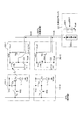
まず構成例1として、図3は、画素回路10と、焼き付きの低減のために考えられた光検出部100を示している。
画素回路10は、駆動トランジスタTd、サンプリングトランジスタTs、保持容量Cs、及び有機EL素子1から成る。このような構成の画素回路10については第1の実施の形態において後述する。
このような画素回路10の有機EL素子1の発光効率の低下を補正するために、固定の電源電圧(Vcc)と光検出線DETL間に光検出素子(光センサ)S1とスイッチングトランジスタT1が挿入された構成の光検出部100を設ける。
First, as a configuration example 1, FIG. 3 shows a
The
In order to correct such a decrease in the light emission efficiency of the
この場合、例えばフォトダイオードによる光センサS1は、有機EL素子1の発光光量に応じたリーク電流を流すことになる。
一般に光を検出するダイオードは光を検出するとその電流が増加する。また、電流の増加量はダイオードに入射する光量によって変化する。具体的には光量が多ければ電流増加量は大きく、少なければ電流増加量は小さくなる。
この光センサS1を流れる電流は、スイッチングトランジスタT1が導通されることで光検出線DETLに流れる。
光検出線DETLに接続された外部ドライバ101は、光センサS1によって光検出線DETLに与えられた電流量を検出する。
外部ドライバ101が検出した電流値は検出情報信号に変換されて水平セレクタ11に供給される。水平セレクタ11では、検出情報信号から、画素回路10に与えた信号値Vsigに対応する検出電流値となっているか否かを判別する。もし有機EL素子1の発光輝度が劣化していると、検出電流量が減少する。そのような場合は、信号値Vsigを補正するようにする。
In this case, for example, the photosensor S <b> 1 using a photodiode passes a leak current according to the light emission amount of the
In general, a diode that detects light increases its current when it detects light. Further, the amount of increase in current varies depending on the amount of light incident on the diode. Specifically, the amount of increase in current is large when the amount of light is large, and the amount of increase in current is small when the amount of light is small.
The current flowing through the photosensor S1 flows to the photodetection line DETL when the switching transistor T1 is turned on.
The
The current value detected by the
図4に光検出動作波形を示す。ここでは、光検出部100が検出電流を外部ドライバ101に出力する期間(光検出期間)を1フレームとしている。
図4の信号書込期間において、画素回路10は走査パルスWSによってサンプリングトランジスタTsがオンとされ、水平セレクタ11によって信号線DTLに与えられている信号値Vsigが入力される。この信号値Vsigは駆動トランジスタTdのゲートに入力され、容量Csに保持される。このため駆動トランジスタTdは、そのゲート・ソース間電圧に応じた電流を有機EL素子1に流し、有機EL素子1を発光させる。例えば現フレームは、白表示のための信号値Vsigが与えられたとすると、有機EL素子1は現フレームにおいて白レベルの発光を行う。
この白レベルの発光が行われるフレームにおいて、光検出部100では制御パルスpT1によってスイッチングトランジスタT1が導通される。このため有機EL素子1の光を受けた光センサS1の電流変化が、光検出線DETLに反映される。
例えばその際の光センサS1に流れる電流量は、本来の発光光量であれば、図4に実線で示すものである場合、有機EL素子1の劣化によって発光光量が低下していれば、例えば点線で示すようになる。
FIG. 4 shows the light detection operation waveform. Here, the period during which the
In the signal writing period of FIG. 4, the
In the frame in which the white level light emission is performed, in the
For example, if the amount of current flowing through the optical sensor S1 at that time is the original amount of emitted light, it is shown by a solid line in FIG. 4. If the amount of emitted light is reduced due to deterioration of the
このような発光輝度の劣化に応じた電流変化が光検出線DETLに現れるため、外部ドライバ101では、この電流量を検出し、劣化具合の情報を得ることができる。そしてそれを水平セレクタ11にフィードバックし、信号値Vsigを補正して、輝度劣化の補正を行う。このようにすれば、焼き付きを低減させることができる。
Since the current change corresponding to the deterioration of the light emission luminance appears on the light detection line DETL, the
しかしながら、このような光検出方式では、次のような不都合な点が生じた。
光センサS1は、有機EL素子1の発光を受光してその電流を増加させる。この光センサS1としてのダイオードは、電流変化が大きいオフ領域(印加電圧:負で0V付近)を用いるのが望ましい。電流変化を的確に検知するためである。
ところが、このときの電流値は増加しているといっても、オン電流に対しては非常に小さいために精度よく輝度変化を検出するためには光検出線DETLの寄生容量を充電する時間が大きくなってしまう。例えば1フレームで精度良く電流変化を検出することは難しい。
この対策として光センサS1のサイズを大きくして電流量を大きくするということが考えられるが、サイズが大きくなるとそれだけ画素アレイ20内での画素レイアウトに対して光検出部100の占める割合は大きくなってしまう。
However, such a light detection method has the following disadvantages.
The optical sensor S1 receives light emitted from the
However, even if the current value at this time is increased, the time for charging the parasitic capacitance of the photodetection line DETL is required to accurately detect the luminance change because the current value is very small with respect to the on-current. It gets bigger. For example, it is difficult to accurately detect a current change in one frame.
As a countermeasure, it is conceivable to increase the current amount by increasing the size of the photosensor S1, but as the size increases, the proportion of the
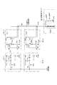
そこで、次に図5のような構成例2としての光検出部200が考えられた。
この光検出部200としての検出信号出力回路は、光センサS1と、容量C1と、nチャネルTFTによる検出信号出力用トランジスタT5,スイッチングトランジスタT3,T4、トランジスタのダイオード接続によるダイオードD1を備える。
Then, next, the
The detection signal output circuit as the
光センサS1は、電源電圧Vccと検出信号出力用トランジスタT5のゲートの間に接続されている。
この光センサS1は一般的にはPINダイオードやアモルファスシリコンを用いて作成される。
この光センサS1は、有機EL素子1で発光される光を検出するように配置されている。そして検出光量に応じて、その電流が増減する。具体的には有機EL素子1の発光光量が多ければ電流増加量は大きく、少なければ電流増加量は小さくなる。
The optical sensor S1 is connected between the power supply voltage Vcc and the gate of the detection signal output transistor T5.
The optical sensor S1 is generally made using a PIN diode or amorphous silicon.
The optical sensor S1 is disposed so as to detect light emitted from the
容量C1は、電源電圧Vccと検出信号出力用トランジスタT5のゲートの間に接続されている。
検出信号出力用トランジスタT5は、ドレインが電源電圧Vccに接続されている。そしてソースがスイッチングトランジスタT3と接続されている。
スイッチングトランジスタT3は、検出信号出力用トランジスタT5のソースと光検出線DETLの間に接続されている。このスイッチングトランジスタT3のゲートは制御線TLxから与えられる制御パルスpT3によってオン/オフされる。スイッチングトランジスタT3がオンとされることで、検出信号出力用トランジスタT5のソース電位が光検出線DETLに出力される構成となっている。
ダイオードD1は、検出信号出力用トランジスタT5のソースとカソード電位Vcatの間に接続されている。
スイッチングトランジスタT4は、そのドレイン及びソースが検出信号出力用トランジスタT5のゲートと基準電位Viniの間に接続されている。このスイッチングトランジスタT4のゲートは、制御線TLyから与えられる制御パルスpT4によってオン/オフされる。
スイッチングトランジスタT4がオンとされることで、検出信号出力用トランジスタT5のゲートに基準電位Viniが入力される構成となっている。
The capacitor C1 is connected between the power supply voltage Vcc and the gate of the detection signal output transistor T5.
The drain of the detection signal output transistor T5 is connected to the power supply voltage Vcc. The source is connected to the switching transistor T3.
The switching transistor T3 is connected between the source of the detection signal output transistor T5 and the light detection line DETL. The gate of the switching transistor T3 is turned on / off by a control pulse pT3 given from the control line TLx. When the switching transistor T3 is turned on, the source potential of the detection signal output transistor T5 is output to the photodetection line DETL.
The diode D1 is connected between the source of the detection signal output transistor T5 and the cathode potential Vcat.
The drain and source of the switching transistor T4 are connected between the gate of the detection signal output transistor T5 and the reference potential Vini. The gate of the switching transistor T4 is turned on / off by a control pulse pT4 given from the control line TLy.
When the switching transistor T4 is turned on, the reference potential Vini is input to the gate of the detection signal output transistor T5.
光検出ドライバ201には、各光検出線DETLについて、その電位を検出する電圧検出部201aが設けられている。この電圧検出部201aによって、光検出部200が出力した検出信号電圧を検出し、これを有機EL素子1の発光光量情報(輝度劣化の情報)として、水平セレクタ11に供給する。
The
図6は光検出動作時の動作波形を示している。
ここでは、画素回路10に信号値Vsigを書き込むための走査パルスWS、光検出部200に対する制御パルスpT4,pT3、検出信号出力用トランジスタT5のゲート電圧、光検出線DETLに表れる電圧を示している。
FIG. 6 shows operation waveforms during the light detection operation.
Here, the scanning pulse WS for writing the signal value Vsig to the
光検出部200では、まず検出準備期間として、制御パルスpT4,pT3によってスイッチングトランジスタT3、T4がオンとされる。このときの状態を図7に示す。
スイッチングトランジスタT4がオンとされることで、基準電圧Viniが検出信号出力用トランジスタT5のゲートに入力する。
ここで基準電圧Viniは検出信号出力用トランジスタT5、及びダイオードD1をオンする電圧とされている。つまり基準電圧Viniは、検出信号出力用トランジスタT5の閾値電圧VthT5、ダイオードD1の閾値電圧VthD1、カソード電圧Vcatの和であるVthT5+VthD1+Vcatより大きい。このため図7のように電流Iiniが流れ、スイッチングトランジスタT3もオンとされているため、光検出線DETLに電位Vxが出力される。
検出準備期間は、このような動作で、図6に示すように、検出信号出力用トランジスタT5のゲート電位=Vini,光検出線DETLの電位=Vxとなる。
In the
When the switching transistor T4 is turned on, the reference voltage Vini is input to the gate of the detection signal output transistor T5.
Here, the reference voltage Vini is a voltage for turning on the detection signal outputting transistor T5 and the diode D1. That is, the reference voltage Vini is larger than VthT5 + VthD1 + Vcat which is the sum of the threshold voltage VthT5 of the detection signal output transistor T5, the threshold voltage VthD1 of the diode D1, and the cathode voltage Vcat. Therefore, the current Iini flows as shown in FIG. 7 and the switching transistor T3 is also turned on, so that the potential Vx is output to the photodetection line DETL.
During the detection preparation period, as shown in FIG. 6, the gate potential of the detection signal output transistor T5 = Vini and the potential of the photodetection line DETL = Vx as shown in FIG.
1フレーム期間の表示のために、画素回路10では信号書込が行われる。即ち図6の信号書込期間において、走査パルスWSがHレベルとされ、サンプリングトランジスタTsが導通される。このとき水平セレクタ11は信号線DTLに白表示階調の信号値Vsigを与えている。これによって当該画素回路10において有機EL素子1で信号値Vsigに応じた発光が行われる。図8にこのときの状態を示す。
このとき、光センサS1は有機EL素子1の発光を受光し、そのリーク電流が変化するが、スイッチングトランジスタT4がオンしているため、検出信号出力用トランジスタT5のゲート電圧は基準電圧Viniのままである。
Signal display is performed in the
At this time, the photosensor S1 receives light emitted from the
信号書込終了後、画素回路10ではサンプリングトランジスタTsがオフとされる。
また光検出部200では、制御パルスpT4がLレベルとされて、スイッチングトランジスタT4がオフとされる。この状態を図9に示す。
スイッチングトランジスタT4がオフとなることで、光センサS1が有機EL素子1の発光を受光し、電源電圧Vccからリーク電流を検出信号出力用トランジスタT5のゲートに流す。
この動作によって検出信号出力用トランジスタT5のゲート電圧は、図6に示すように基準電圧Viniから上昇してゆき、それに伴って光検出線DETLの電位も電位Vxから増加してゆく。この光検出線DETLの電位変化を、電圧検出部201aが検出する。この検出電位は、有機EL素子1の発光光量に応じたものとなる。換言すれば、特定の階調表示(例えば白表示)を画素回路10で実行させているのであれば、検出電位は、有機EL素子1の劣化具合を表すものとなる。例えば光検出線DETLの電位変化として図6の実線は劣化がないとき、破線は劣化が生じているときとしている。
一定時間経過後、制御パルスpT3がLレベルとされ、スイッチングトランジスタT3がオフとされて検出動作を終了する。
例えば1フレームでの該当ラインの各画素回路10についての検出が以上のように行われる。
After the signal writing is completed, the sampling transistor Ts is turned off in the
In the
When the switching transistor T4 is turned off, the optical sensor S1 receives light emitted from the
By this operation, the gate voltage of the detection signal output transistor T5 rises from the reference voltage Vini as shown in FIG. 6, and accordingly, the potential of the photodetection line DETL also increases from the potential Vx. The
After a certain period of time, the control pulse pT3 is set to L level, the switching transistor T3 is turned off, and the detection operation is finished.
For example, the detection of each
この光検出部200の検出信号出力回路構成は、ソースフォロワ回路となっており、検出信号出力用トランジスタT5のゲート電圧が変動すればその変動分がソースに出力される構成となっている。つまり光センサS1のリーク電流変化による検出信号出力用トランジスタT5のゲート電圧の変化がソースから光検出線DETLに出力される。
また、検出信号出力用トランジスタT5のゲート・ソース間電圧Vgsは、その閾値電圧Vthよりも大きくなるように設定されている。このため、出力される電流値は先に図3に示した回路構成と比較して非常に大きく、光センサS1の電流値が小さくても検出信号出力用トランジスタT5を介することで、発光光量の検出情報を光検出ドライバ201に出力することが可能となっている。
The detection signal output circuit configuration of the
The gate-source voltage Vgs of the detection signal output transistor T5 is set to be larger than the threshold voltage Vth. For this reason, the output current value is very large as compared with the circuit configuration shown in FIG. Detection information can be output to the
このため、精度の良い光検出動作が可能であるが、光検出部200は、その素子数が多くなってしまう。即ちセンサS1、4つのトランジスタ(T3,T4,T5,D1)、容量C1が必要であり、画素回路10も含めて、画素当たりの素子数の増大、トランジスタの割合の増大が生じ、低歩留まりの原因となってしまう。
For this reason, an accurate light detection operation is possible, but the number of elements of the
さらに構成例3を図10に示す。
図10の光検出部300は、センサ兼用トランジスタT10と、容量C2と、nチャネルTFTによる検出信号出力用トランジスタT5,スイッチングトランジスタT3を備える。
Further, Configuration Example 3 is shown in FIG.
10 includes a sensor serving transistor T10, a capacitor C2, a detection signal output transistor T5 using an n-channel TFT, and a switching transistor T3.
センサ兼用トランジスタT10は、電源線VLと検出信号出力用トランジスタT5のゲートの間に接続されている。
このセンサ兼用トランジスタT10は、上記図5の構成のダイオードによる光センサS1に代えるものであり、オン状態及びオフ状態とされてスイッチ素子として機能するとともにオフ状態において光センサとして機能する。
TFTは、その構造としてチャネル層に対してゲートメタル、ソースメタル等が配されて形成される。センサ兼用トランジスタT10は、例えばソース、ドレインを形成するメタル層がチャネル層の上方においてチャネル層を比較的遮光しない構造とすることで形成できる。つまり外光がチャネル層に入射されるようにTFTを形成すればよい。
このセンサ兼用トランジスタT10は、有機EL素子1で発光される光を検出するように配置されている。そしてオフ状態において、受光光量に応じて、そのリーク電流が増減する。具体的には有機EL素子1の発光光量が多ければリーク電流の増加量は大きく、少なければリーク電流の増加量は小さくなる。
またセンサ兼用トランジスタT10のゲートは、制御線TLbに接続され、制御パルスpT10によってオン/オフされる。センサ兼用トランジスタT10がオンとされることで、検出信号出力用トランジスタT5のゲートに電源線VLの電位が入力される構成となっている。
The sensor serving transistor T10 is connected between the power supply line VL and the gate of the detection signal outputting transistor T5.
This sensor serving transistor T10 replaces the light sensor S1 using the diode having the configuration shown in FIG. 5, and functions as a switch element in an on state and an off state, and also functions as a light sensor in the off state.
The TFT has a structure in which a gate metal, a source metal, and the like are arranged on a channel layer. The sensor serving transistor T10 can be formed by, for example, a structure in which a metal layer forming a source and a drain does not shield the channel layer above the channel layer. That is, a TFT may be formed so that external light is incident on the channel layer.
The sensor serving transistor T10 is arranged to detect light emitted from the
The gate of the sensor serving transistor T10 is connected to the control line TLb and turned on / off by the control pulse pT10. When the sensor serving transistor T10 is turned on, the potential of the power supply line VL is input to the gate of the detection signal outputting transistor T5.
電源線VLには、電源電圧Vccと基準電圧Viniという2つの値を持つパルス電圧が、検出動作制御部21によって与えられる。
容量C2は、カソード電位Vcatと検出信号出力用トランジスタT5のゲートの間に接続されている。この容量C2は検出信号出力用トランジスタT5のゲート電圧を保持するために設けられる。
A pulse voltage having two values of a power supply voltage Vcc and a reference voltage Vini is applied to the power supply line VL by the detection
The capacitor C2 is connected between the cathode potential Vcat and the gate of the detection signal output transistor T5. The capacitor C2 is provided to hold the gate voltage of the detection signal output transistor T5.
検出信号出力用トランジスタT5は、ドレインが電源線VLに接続されている。そしてソースがスイッチングトランジスタT3と接続されている。
スイッチングトランジスタT3は、検出信号出力用トランジスタT5のソースと光検出線DETLの間に接続されている。このスイッチングトランジスタT3のゲートは制御線TLaに接続され、制御パルスpT3によってオン/オフされる。スイッチングトランジスタT3がオンとされることで、検出信号出力用トランジスタT5を流れる電流が光検出線DETLに出力される構成となっている。
The drain of the detection signal output transistor T5 is connected to the power supply line VL. The source is connected to the switching transistor T3.
The switching transistor T3 is connected between the source of the detection signal output transistor T5 and the light detection line DETL. The gate of the switching transistor T3 is connected to the control line TLa and is turned on / off by the control pulse pT3. When the switching transistor T3 is turned on, the current flowing through the detection signal output transistor T5 is output to the photodetection line DETL.
光検出ドライバ301には、各光検出線DETLについて、その電位を検出する電圧検出部301aが設けられている。この電圧検出部301aによって、光検出部300が出力した検出信号電圧を検出する。
なお、光検出線DETLには、例えばダイオード接続のトランジスタによるダイオードD1が接続され、固定電位(例えばカソード電位Vcat)への電流経路を設けている。
The
For example, a diode D1 formed of a diode-connected transistor is connected to the light detection line DETL, and a current path to a fixed potential (for example, a cathode potential Vcat) is provided.
図11〜図16で光検出部300による光検出動作について説明する。
図11に光検出部300の動作に関する波形を示す。ここではライトスキャナ12が画素回路10(サンプリングトランジスタTs)に与える走査パルスWSを示している。また、制御線TLb,TLaに与えられる制御パルスpT10,pT3、電源線VLの電源パルスも示している。また検出信号出力用トランジスタT5のゲート電圧、光検出線DETLに表れる電圧も示している。
そして1つの光検出部300は、対応する画素回路10についての光量検出を、図11のように1フレームの期間で行う例とする。
The light detection operation by the
FIG. 11 shows waveforms relating to the operation of the
One
まず検出準備期間を含む時点tm0〜tm6の間、電源線VLは基準電圧Viniとされる。そして、時点tm1〜tm5で制御パルスpT10がHレベルとされ、センサ兼用トランジスタT10がオンとされて検出準備が行われる。
このときの状態を図12に示す。電源線VLが基準電圧Viniとされている時点tm1でセンサ兼用トランジスタT10がオンすることで、検出信号出力用トランジスタT5のゲートに基準電圧Viniが入力される。また時点tm2で制御パルスpT3によりスイッチングトランジスタT3がオンされることで、検出信号出力用トランジスタT5のソースが光検出線DETLに接続される。
ここで基準電圧Viniは検出信号出力用トランジスタT5をオンする電圧とされている。このため図12のように電流Iiniが流れ、光検出線DETLは或る電位Vxとなる。検出準備期間ではこのような動作が行われることで、図11に示すように、検出信号出力用トランジスタT5のゲート電位=Vini,光検出線DETLの電位=Vxとなる。
First, between time points tm0 to tm6 including the detection preparation period, the power supply line VL is set to the reference voltage Vini. At time points tm1 to tm5, the control pulse pT10 is set to the H level, the sensor serving transistor T10 is turned on, and preparation for detection is performed.
The state at this time is shown in FIG. The sensor serving transistor T10 is turned on at time tm1 when the power supply line VL is set to the reference voltage Vini, whereby the reference voltage Vini is input to the gate of the detection signal output transistor T5. At the time tm2, the switching transistor T3 is turned on by the control pulse pT3, so that the source of the detection signal output transistor T5 is connected to the light detection line DETL.
Here, the reference voltage Vini is a voltage for turning on the detection signal outputting transistor T5. Therefore, the current Iini flows as shown in FIG. 12, and the light detection line DETL becomes a certain potential Vx. By performing such an operation in the detection preparation period, as shown in FIG. 11, the gate potential of the detection signal output transistor T5 = Vini and the potential of the photodetection line DETL = Vx.
図11の時点tm3〜tm4は、1フレーム期間の表示のために、画素回路10に対して信号値Vsigの書込が行われる。即ち信号書込期間において、走査パルスWSがHレベルとされ、サンプリングトランジスタTsが導通される。このとき水平セレクタ11は信号線DTLに例えば白表示階調の信号値Vsigを与えている。これによって当該画素回路10において有機EL素子1で信号値Vsigに応じた発光が行われる。図13にこのときの状態を示す。
このときセンサ兼用トランジスタT10がオンしているため、検出信号出力用トランジスタT5のゲート電圧は基準電圧Viniのままである。
At time points tm3 to tm4 in FIG. 11, the signal value Vsig is written to the
At this time, since the sensor serving transistor T10 is on, the gate voltage of the detection signal outputting transistor T5 remains the reference voltage Vini.
信号書込終了後、時点tm4で画素回路10ではサンプリングトランジスタTsがオフとされる。
また光検出部300では、時点tm5で制御パルスpT10がLレベルとされて、センサ兼用トランジスタT10がオフとされる。この状態を図14に示す。
センサ兼用トランジスタT10をオフすることで、検出信号出力用トランジスタT5のゲートには、容量C2とセンサ兼用トランジスタT10の寄生容量との容量比に応じたΔVa’というカップリング量が入力される。このため光検出線DETLの電圧もVx−ΔVaという電位に変化する。
カップリングによってセンサ兼用トランジスタT10のソース・ドレイン間には電位差が生じ、受光した光量によってそのリーク量を変化させる。しかしこのときのリーク電流によっては、検出信号出力用トランジスタT5のゲート電圧は殆ど変化しない。これはセンサ兼用トランジスタT10のソース・ドレイン間の電位差が小さいのと、次動作である電源線VLを基準電圧Viniから電源電圧Vccへ変化させる動作までの時間が短いことによる。
After completion of signal writing, the sampling transistor Ts is turned off in the
In the
By turning off the sensor serving transistor T10, a coupling amount of ΔVa ′ corresponding to the capacitance ratio between the capacitor C2 and the parasitic capacitance of the sensor serving transistor T10 is input to the gate of the detection signal outputting transistor T5. For this reason, the voltage of the photodetection line DETL also changes to a potential of Vx−ΔVa.
Due to the coupling, a potential difference is generated between the source and drain of the sensor serving transistor T10, and the amount of leakage is changed depending on the amount of received light. However, depending on the leakage current at this time, the gate voltage of the detection signal output transistor T5 hardly changes. This is because the potential difference between the source and the drain of the sensor serving transistor T10 is small and the time until the next operation of changing the power supply line VL from the reference voltage Vini to the power supply voltage Vcc is short.
一定時間経過した時点tm6で、電源線VLは基準電圧Viniから電源電圧Vccとされる。
この動作によって、検出信号出力用トランジスタT5のゲートに電源線VLからのカップリングが入力され、検出信号出力用トランジスタT5のゲート電位は上昇する。また、電源線VLが高電位へ変化することで、センサ兼用トランジスタT10のソース・ドレイン間に大きな電位差が生じ、受光した光量によって電源線VLから検出信号出力用トランジスタT5のゲートにリーク電流が流れる。
この状態を図15に示す。この動作によって、検出信号出力用トランジスタT5のゲート電圧はVini−ΔVa’から、Vini−ΔVa’+ΔV’となる。図11には、検出信号出力用トランジスタT5のゲート電圧が、時点tm6以降、Vini−ΔVa’から、Vini−ΔVa’+ΔV’に上昇していく様子を示している。
また、それに伴って光検出線DETLの電位も電位Vx−ΔVaから上昇していき、V0+ΔVとなる。なお、V0とは、低階調表示(黒表示)のときの光検出線DETLの電位としている。センサ兼用トランジスタT10が受光する光量が多いほど、そこに流れる電流量は多くなるため、高階調表示時における光検出線DETLの電圧は、低階調表示時における電圧よりも大きくなる。
At a time point tm6 when a certain time has elapsed, the power supply line VL is changed from the reference voltage Vini to the power supply voltage Vcc.
By this operation, the coupling from the power supply line VL is input to the gate of the detection signal output transistor T5, and the gate potential of the detection signal output transistor T5 rises. Further, when the power supply line VL changes to a high potential, a large potential difference occurs between the source and drain of the sensor serving transistor T10, and a leak current flows from the power supply line VL to the gate of the detection signal output transistor T5 depending on the amount of received light. .
This state is shown in FIG. By this operation, the gate voltage of the detection signal outputting transistor T5 is changed from Vini−ΔVa ′ to Vini−ΔVa ′ + ΔV ′. FIG. 11 shows how the gate voltage of the detection signal output transistor T5 increases from Vini−ΔVa ′ to Vini−ΔVa ′ + ΔV ′ after time tm6.
Along with this, the potential of the light detection line DETL also rises from the potential Vx−ΔVa and becomes V0 + ΔV. Note that V0 is the potential of the photodetection line DETL at the time of low gradation display (black display). As the amount of light received by the sensor serving transistor T10 increases, the amount of current flowing therethrough increases, and therefore the voltage of the light detection line DETL at the time of high gradation display becomes larger than the voltage at the time of low gradation display.
この光検出線DETLの電位変化を、電圧検出部301aが検出する。この検出電圧は、有機EL素子1の発光光量に応じたものとなる。換言すれば、特定の階調表示(例えば白表示)を画素回路10で実行させているのであれば、検出電位は、有機EL素子1の劣化具合を表すものとなる。
一定時間経過後、時点tm7で制御パルスpT3がLレベルとされ、スイッチングトランジスタT3がオフとされて検出動作を終了する。これにより光検出線には電流が供給されることがなくなり、その電位はVcat+VthD1という電位になる。なおVthD1はダイオードD1の閾値電圧である。
例えば1フレームでの該当ラインの各画素回路10についての検出が以上のように行われる。
The
After a certain period of time, at time tm7, the control pulse pT3 is set to L level, the switching transistor T3 is turned off, and the detection operation is finished. As a result, no current is supplied to the photodetection line, and the potential is Vcat + VthD1. VthD1 is a threshold voltage of the diode D1.
For example, the detection of each
以上のような光検出動作を行う光検出部300では、図5で述べた光検出部200と同様に精度の良い光検出動作が可能である。
そしてセンサ兼用トランジスタT10を用いることで、素子数の削減を行うことができる。しかしながら、2つのトランジスタT10、T3に対する制御線TLb,TLaが必要であること、及び電源線VLをパルス電圧電源とすることで、1つの光検出部300に対して3系統の制御系が必要になる。
In the
By using the sensor serving transistor T10, the number of elements can be reduced. However, the need for the control lines TLb and TLa for the two transistors T10 and T3 and the use of the power supply line VL as a pulse voltage power supply necessitates a three-system control system for one
例えば以上の構成例2,3では、高精度の検出が可能ではあるが、構成例2の場合、光検出部200の素子数が多くなり、構成例3では、素子数は減少するものの、制御線が3系統(つまり制御線を駆動するドライバの増加)という短所がある。
本発明の実施の形態では、このような点を踏まえ、構成例2、構成例3のように精度良く光検出を行うことができることを維持しながら、光検出部やその制御系の構成を簡易化し、高歩留まりを実現できるようにする。
For example, in the above configuration examples 2 and 3, high-precision detection is possible, but in the configuration example 2, the number of elements of the
In the embodiment of the present invention, based on such points, the configuration of the light detection unit and its control system can be simplified while maintaining that light detection can be performed with high accuracy as in Configuration Example 2 and Configuration Example 3. To achieve a high yield.
<3.第1の実施の形態>
[3−1 回路構成]
図1に示した実施の形態の画素回路10及び光検出部30の構成を図16に示す。
なお、ここでは同じ信号線DTLに接続される2つの画素回路10(10−1、10−2)、及び各画素回路10−1、10−2に対応し、同じ光検出線DETLに接続される2つの光検出部30(30−1、30−2)を示している。以下、特に区別が必要な場合を除いては、まとめて「画素回路10」「光検出部30」と表記する。
<3. First Embodiment>
[3-1 Circuit configuration]
The configuration of the
Here, the two pixel circuits 10 (10-1, 10-2) connected to the same signal line DTL and the pixel circuits 10-1, 10-2 are connected to the same light detection line DETL. The two light detection parts 30 (30-1, 30-2) are shown. Hereinafter, unless otherwise particularly required, they are collectively referred to as “
図16の画素回路10は、nチャネルTFTによるサンプリングトランジスタTs、保持容量Cs、pチャネルTFTによる駆動トランジスタTd、有機EL素子1を有する。
図1で示したように各画素回路10は、信号線DTLと書込制御線WSLとの交差部に配される。信号線DTLはサンプリングトランジスタTsのドレインに接続され、書込制御線WSLはサンプリングトランジスタTsのゲートに接続されている。
The
As shown in FIG. 1, each
駆動トランジスタTd及び有機EL素子1は、電源電位Vccとカソード電位Vcatの間で直列に接続されている。
またサンプリングトランジスタTs及び保持容量Csは、駆動トランジスタTdのゲートに接続されている。駆動トランジスタTdのゲート・ソース間電圧をVgsで表わしている。
The drive transistor Td and the
The sampling transistor Ts and the storage capacitor Cs are connected to the gate of the drive transistor Td. The gate-source voltage of the drive transistor Td is represented by Vgs.
この画素回路10では、水平セレクタ11が信号線DTLに輝度信号に応じた信号値を印加するときに、ライトスキャナ12が書込制御線WSLの走査パルスWSをHレベルとすると、サンプリングトランジスタTsが導通して信号値が保持容量Csに書き込まれる。保持容量Csに書き込まれた信号値電位が駆動トランジスタTdのゲート電位となる。
ライトスキャナ12が書込制御線WSLの走査パルスWSをLレベルとすると、信号線DTLと駆動トランジスタTdとは電気的に切り離されるが、駆動トランジスタTdのゲート電位は保持容量Csによって安定に保持される。
そして電源電位Vccからカソード電位Vcatに向かって駆動電流Idsが駆動トランジスタTd及び有機EL素子1に流れる。
このとき電流Idsは、駆動トランジスタTdのゲート・ソース間電圧Vgsに応じた値となり、有機EL素子1はその電流値に応じた輝度で発光する。
つまりこの画素回路10では、保持容量Csに信号線DTLからの信号値電位を書き込むことによって駆動トランジスタTdのゲート印加電圧を変化させ、これにより有機EL素子1に流れる電流値をコントロールして発色の階調を得る。
In the
When the
A drive current Ids flows from the power supply potential Vcc to the cathode potential Vcat through the drive transistor Td and the
At this time, the current Ids has a value corresponding to the gate-source voltage Vgs of the drive transistor Td, and the
In other words, in this
pチャネルTFTによる駆動トランジスタTdのソースは電源電圧Vccに接続されており、常に飽和領域で動作するように設計されているので、駆動トランジスタTdは次の式1に示した値を持つ定電流源となる。
Ids=(1/2)・μ・(W/L)・Cox・(Vgs−Vth)2・・・(式1)
但し、Idsは飽和領域で動作するトランジスタのドレイン・ソース間に流れる電流、μは移動度、Wはチャネル幅、Lはチャネル長、Coxはゲート容量、Vthは駆動トランジスタTdの閾値電圧を表している。
この式1から明らかな様に、飽和領域ではトランジスタのドレイン電流Idsはゲート・ソース間電圧Vgsによって制御される。駆動トランジスタTdは、ゲート・ソース間電圧Vgsが一定に保持される為、定電流源として動作し、有機EL素子1を一定の輝度で発光させることができる。
Since the source of the drive transistor Td by the p-channel TFT is connected to the power supply voltage Vcc and is always designed to operate in the saturation region, the drive transistor Td is a constant current source having the value shown in the
Ids = (1/2) · μ · (W / L) · Cox · (Vgs−Vth) 2 (Equation 1)
Where Ids is the current flowing between the drain and source of a transistor operating in the saturation region, μ is the mobility, W is the channel width, L is the channel length, Cox is the gate capacitance, and Vth is the threshold voltage of the driving transistor Td. Yes.
As is apparent from
ここで一般的に、有機EL素子1の電流−電圧特性は時間が経過すると劣化してしまう。そして画素回路10においては、有機EL素子1の経時変化とともに、駆動トランジスタTdのドレイン電圧が変化してゆく。ところが画素回路10ではゲート・ソース間電圧Vgsが一定であるので、有機EL素子1には一定量の電流が流れ、発光輝度は変化しない。つまり安定した階調制御ができる。
Here, in general, the current-voltage characteristics of the
しかしながら、有機EL素子1は時間変化と共にその駆動電圧だけでなく、発光効率も低下してしまう。つまり同じ電流を流してもその発光輝度が時間と共に低下してしまうこととなる。その結果、上述した図59(a)のように焼き付きが発生してしまう。
そこで光検出部30を設け、発光輝度の劣化に応じた補正が行われるようにしている。
本例の光検出部30は、図16に示すようにセンサ兼用トランジスタT10と、容量C2と、nチャネルTFTによる検出信号出力用トランジスタT5のみで構成される。
However, as the
Therefore, the
As shown in FIG. 16, the
センサ兼用トランジスタT10は、電源線VLと検出信号出力用トランジスタT5のゲートの間に接続されている。
このセンサ兼用トランジスタT10は、上記図5の構成のダイオードによる光センサS1に代えるものであり、オン状態及びオフ状態とされてスイッチ素子として機能するとともにオフ状態において光センサとして機能する。
このセンサ兼用トランジスタT10は、有機EL素子1で発光される光を検出するように配置されている。そしてオフ状態において、受光光量に応じて、そのリーク電流が増減する。具体的には有機EL素子1の発光光量が多ければリーク電流の増加量は大きく、少なければリーク電流の増加量は小さくなる。
またセンサ兼用トランジスタT10のゲートは、制御線TLbに接続されている。従って図1に示した検出動作制御部21の制御パルスpT10によってオン/オフされる。センサ兼用トランジスタT10がオンとされることで、検出信号出力用トランジスタT5のゲートに電源線VLの電圧が入力される構成となっている。
なお、図1で述べたように、電源線VLには、電源電圧Vccと基準電圧Viniという2つの値を持つパルス電圧が、検出動作制御部21によって与えられる。
The sensor serving transistor T10 is connected between the power supply line VL and the gate of the detection signal outputting transistor T5.
This sensor serving transistor T10 replaces the light sensor S1 using the diode having the configuration shown in FIG. 5, and functions as a switch element in an on state and an off state, and also functions as a light sensor in the off state.
The sensor serving transistor T10 is arranged to detect light emitted from the
The gate of the sensor serving transistor T10 is connected to the control line TLb. Therefore, it is turned on / off by the control pulse pT10 of the detection
As described with reference to FIG. 1, a pulse voltage having two values of the power supply voltage Vcc and the reference voltage Vini is applied to the power supply line VL by the detection
容量C2は、カソード電位Vcatと検出信号出力用トランジスタT5のゲートの間に接続されている。この容量C2は検出信号出力用トランジスタT5のゲート電圧を保持するために設けられる。
検出信号出力用トランジスタT5は、ドレインが電源線VLに接続されている。そしてソースが光検出線DETLに接続されている。
The capacitor C2 is connected between the cathode potential Vcat and the gate of the detection signal output transistor T5. The capacitor C2 is provided to hold the gate voltage of the detection signal output transistor T5.
The drain of the detection signal output transistor T5 is connected to the power supply line VL. The source is connected to the light detection line DETL.
光検出ドライバ22には、各光検出線DETLについて、その電位を検出する電圧検出部22aが設けられている。この電圧検出部22aによって、光検出部30が出力した検出信号電圧を検出し、これを有機EL素子1の発光光量情報(輝度劣化の情報)として、図1の水平セレクタ11(信号値補正部11a)に供給する。
なお、光検出線DETLには、例えばダイオード接続のトランジスタによるダイオードD1が接続され、固定電位(例えばカソード電位Vcat)への電流経路を設けている。
これは、図5における光検出部200内のダイオードD1を画素アレイ20の外部(光検出ドライバ22側)に配置するものであり、本例の光検出部30の素子数の削減のための一要素となっている。
The
For example, a diode D1 formed of a diode-connected transistor is connected to the light detection line DETL, and a current path to a fixed potential (for example, a cathode potential Vcat) is provided.
This is to dispose the diode D1 in the
このように本例の光検出部30では、センサ兼用トランジスタT10を設けること、及びダイオードD1を外部配置すること、検出信号出力用トランジスタT5を光検出線DETLに直接接続することで、2つのトランジスタ(T5,T10)と容量C2によって構成されるようにしている。さらに、1つの光検出部30に対する制御線は、センサ兼用トランジスタT10をオン/オフ制御するための制御パルスpT10を与える制御線TLbと、パルス電圧を与える電源線VLの2系統のみとなる。
As described above, in the
[3−2 光検出動作期間]
図16に示した光検出部30によって、画素回路10の有機EL素子1の発光光量を検出する光検出動作が行われるが、まずここで、光検出部30の光検出動作等の実行期間について説明する。
なお、ここで説明する光検出動作期間は、後述する第2〜第7の実施の形態でも同様となる。
[3-2 Photodetection operation period]
The
The light detection operation period described here is the same in the second to seventh embodiments described later.
図17(a)は、通常映像表示終了後に光検出動作を行う例を示している。
なお、「通常映像表示」とは、表示装置に供給された映像信号に基づく信号値Vsigを各画素回路10に与えて、通常の動画や静止画としての映像表示を行っている状態を言うこととする。
FIG. 17A shows an example in which the light detection operation is performed after the normal video display ends.
Note that “normal video display” refers to a state in which a signal value Vsig based on a video signal supplied to the display device is given to each
図17(a)の場合、時点t0で表示装置の電源がオンとされたとする。
ここで時点t1までに電源投入時の各種初期動作が行われ、時点t1から通常映像表示を開始するとする。そして時点t1以降、通常映像表示として、映像のフレームF1,F2・・・の表示が実行される。
この間、光検出部30は光検出動作は行わない。
時点t2で通常映像表示が終了されるとする。例えば電源オフ操作が行われた場合などである。
この図17(a)の例の場合、この時点t2以降で光検出部30が光検出動作を実行する。
この場合、例えば1フレーム期間に1ライン分の画素についての光検出動作を行う。
例えば光検出動作を開始する場合、水平セレクタ11は最初のフレームFaでは、図17(b)に示すように1ライン目を白表示とするような表示を各画素回路10に実行させる。つまり1ライン目の画素回路10のみ白表示(高輝度階調表示)を行わせ、他の全ての画素回路10には黒表示を実行させるように、各画素回路10に信号値Vsigを与える。
このフレームFaの期間において、1ライン目の画素に対応する各光検出部30は、対応する画素の発光光量を検出する。光検出ドライバ22は、各列の光検出線DETLの電圧検出を行い、1ライン目の各画素の発光輝度情報を得る。そして、それを水平セレクタ11にフィードバックする。
In the case of FIG. 17A, it is assumed that the power of the display device is turned on at time t0.
Here, various initial operations at the time of power-on are performed by time t1, and normal video display is started from time t1. After time t1, display of video frames F1, F2,... Is executed as normal video display.
During this time, the
It is assumed that the normal video display ends at time t2. For example, when a power-off operation is performed.
In the case of the example of FIG. 17A, the
In this case, for example, the light detection operation is performed on pixels for one line in one frame period.
For example, when the light detection operation is started, the
In the period of the frame Fa, each
次のフレームFbでは、水平セレクタ11は図17(b)に示すように2ライン目を白表示とするような表示を各画素回路10に実行させる。つまり2ライン目の画素回路10のみ白表示(高輝度階調表示)を行わせ、他の全ての画素回路10には黒表示を実行させる。
このフレームFbの期間において、2ライン目の画素に対応する光検出部30は、対応する画素の発光光量を検出する。光検出ドライバ22は、各列の光検出線DETLの電圧検出を行い、2ライン目の各画素の発光輝度情報を得る。そして、それを水平セレクタ11にフィードバックする。
このような動作を、最終ラインまで続けていく。最終ラインの各画素の発光輝度情報を検出し、水平セレクタ11にフィードバックした段階で、光検出動作は終了する。
水平セレクタ11は、各画素の発光輝度情報に基づいて信号値補正処理を行う。
時点t3で以上の光検出動作が完了したら、例えば表示装置の電源をオフにするなど、所要の処理を行う。
In the next frame Fb, the
In the period of the frame Fb, the
Such an operation is continued until the final line. At the stage where the light emission luminance information of each pixel in the final line is detected and fed back to the
The
When the above light detection operation is completed at time t3, for example, a necessary process is performed such as turning off the power of the display device.
なお、各ラインの光検出動作において、該当ラインの画素に対応する光検出部30が選択されるが、その選択は、検出動作制御部21が電源線VLに与える電源パルスと、センサ兼用トランジスタT10に対する制御パルスpT10によって行われる。
即ち各フレームで、該当ラインの画素に対応する光検出部30のみによる光検出に応じた電圧変化が光検出線DETL上に表れるように、各光検出部30の動作が制御される。
Note that, in the light detection operation of each line, the
That is, in each frame, the operation of each
図18(a)は、通常映像表示実行中に、或る周期で光検出動作を行う例である。
例えば時点t10で通常映像表示が開始されたとする。光検出部30による光検出動作は、この通常映像表示の開始とともに、1フレームの期間に1ライン毎行われる。即ち上記図17の時点t2〜t3で示した動作と同様の検出動作を行う。但し、各画素回路10の表示は通常の映像表示の状態であり、図17(b)のような光検出動作用の表示ではない。
1ライン目〜最終ラインまでについての光検出動作を完了したら、一旦、光検出部30は光検出動作を終了する。
FIG. 18A shows an example in which the light detection operation is performed at a certain period during the normal video display execution.
For example, assume that normal video display is started at time t10. The light detection operation by the
When the light detection operation for the first line to the last line is completed, the
光検出動作は、所定周期毎に行うものとし、ある時点t12で、その検出動作周期のタイミングに至ったとすると、その時点t12から、同様に1ライン目〜最終ラインまでの光検出動作を行う。そして光検出動作を完了したら、その後所定期間、光検出動作を行わない。
例えばこのように、通常映像表示実行中に並行して、所定周期で光検出動作を行うことも考えられる。
It is assumed that the light detection operation is performed every predetermined cycle. If the detection operation cycle timing is reached at a certain time t12, the light detection operation from the first line to the last line is similarly performed from that time t12. When the light detection operation is completed, the light detection operation is not performed for a predetermined period thereafter.
For example, in this way, it is conceivable to perform the light detection operation in a predetermined cycle in parallel with the normal video display execution.
図18(b)は、電源オン時に光検出動作を行う例である。
時点t20で表示装置の電源がオンとされたとする。ここで電源投入時の立ち上げ等の各種初期動作が行われた直後、時点t21から光検出動作を行う。即ち上記図17(a)の時点t2〜t3で示した動作と同様の検出動作を行う。各画素回路10についても、図17(b)のように、各フレーム毎に、1ラインのみ白表示とする光検出動作用の表示を実行させる。
FIG. 18B shows an example in which the light detection operation is performed when the power is turned on.
It is assumed that the display device is turned on at time t20. Here, immediately after various initial operations such as start-up when the power is turned on, the light detection operation is performed from time t21. That performs the operation similar to the detection operation shown at t2~t3 of FIG 17 (a). Also for each
1ライン目〜最終ラインまでについての光検出動作を完了したら、時点t22で、水平セレクタ11は各画素回路10に対して通常映像表示を開始させる。光検出部30では光検出動作を行わない。
When the light detection operation from the first line to the last line is completed, the
例えば以上のように、通常映像表示終了後、通常映像表示実行中、通常の映像表示開始前などに、光検出動作を行い、その検出に基づいて信号値補正処理を行うことで、発光輝度劣化に対応できる。
なお、例えば通常映像表示終了後と通常の映像表示開始前の両方で光検出動作を行うような例も考えられる。
For example, as described above, after the normal video display is finished, during the normal video display execution, before the normal video display start, etc., the light detection operation is performed, and the signal value correction processing is performed based on the detection, thereby deteriorating the emission luminance. It can correspond to.
An example in which the light detection operation is performed both after the end of normal video display and before the start of normal video display is also conceivable.
通常映像表示終了後と通常の映像表示開始前の一方、又は両方で光検出動作を行う場合は、図17(b)に示したような光検出動作用の表示を実行できるので、その白表示などの高い階調の発光で検出ができるという利点がある。また任意の階調の表示を実行させて階調毎の劣化具合を検出するようにもできる。
一方、通常映像表示実行中に行う場合、実際に表示中の映像内容は不定であるため、階調を特定して光検出動作を行うことができない。このため、検出値は、発光階調(その際に検出対象画素に与えた信号値Vsig)を考慮したものとして判定し、信号値補正処理を行う必要がある。但し、通常映像表示実行中に繰り返し光検出動作及び補正処理ができることで、有機EL素子1の輝度劣化に対して、ほぼ常時対応できるという利点がある。
When the light detection operation is performed after one or both of the normal image display and the normal image display start, the display for the light detection operation as shown in FIG. 17B can be executed. There is an advantage that detection is possible with light emission of high gradation. It is also possible to execute display of any gradation and detect the degree of deterioration for each gradation.
On the other hand, when it is performed during execution of normal video display, the actual video content being displayed is indefinite, so that it is not possible to perform light detection operation by specifying the gradation. For this reason, it is necessary to determine the detection value as considering the light emission gradation (the signal value Vsig given to the detection target pixel at that time), and to perform signal value correction processing. However, since the light detection operation and the correction process can be repeatedly performed during the normal video display execution, there is an advantage that the luminance degradation of the
[3−3 光検出動作]
図19〜図25で第1の実施の形態の光検出部30による光検出動作について説明する。例えば上記図17の通常映像表示終了後などに実行する動作である。
[3-3 Light detection operation]
The light detection operation by the
図19には、画素回路10−1,10−2に対する走査パルスWS、光検出部30−1に対する制御パルスpT10、光検出部30−2に対する制御パルスpT10をそれぞれ示している。例えば図17のように、通常映像表示終了後などに1ライン毎に光検出を行うものとし、1回の検出は1フレームで行うとした例である。
即ち、画素回路10−1において、或るタイミングで信号値Vsigの書込が行われ1フレームの発光が行われるが、そのときに光検出部30−1では、制御パルスpT10及び電源線VLのパルス電圧に応じて光検出動作が行われる。
次のフレーム期間では、画素回路10−2において、或るタイミングで信号値Vsigの書込が行われ1フレームの発光が行われ、そのときに光検出部30−2では制御パルスpT10及び電源線VLのパルス電圧に応じて光検出動作が行われる。
FIG. 19 shows a scanning pulse WS for the pixel circuits 10-1 and 10-2, a control pulse pT10 for the light detection unit 30-1, and a control pulse pT10 for the light detection unit 30-2. For example, as shown in FIG. 17, light detection is performed for each line after the end of normal video display, and one detection is performed for one frame.
That is, in the pixel circuit 10-1, the signal value Vsig is written at a certain timing and light emission of one frame is performed. At that time, the light detection unit 30-1 performs the control pulse pT10 and the power supply line VL. The light detection operation is performed according to the pulse voltage.
In the next frame period, in the pixel circuit 10-2, the signal value Vsig is written at a certain timing and light emission of one frame is performed. At that time, the light detection unit 30-2 controls the control pulse pT10 and the power supply line. The light detection operation is performed according to the pulse voltage of VL.
画素回路10−1、光検出部30−1側に注目して、図20〜図25により、光検出動作を詳しく述べる。
図20には、光検出部30−1の動作に関する波形として、ライトスキャナ12が画素回路10−1(サンプリングトランジスタTs)に与える走査パルスWSを示している。
また、電源線VLの電源パルスも示している。図のように検出動作制御部21は、光検出期間に先立つ検出準備期間に、電源線VLに基準電圧Viniを与えており、光検出を実行する期間には電源線VLに電源電圧Vccを与える。
また、検出動作制御部21が、制御線TLb1に与える制御パルスpT10を示している。制御パルスpT10によって光検出部30のセンサ兼用トランジスタT10がオン/オフされる。
また検出信号出力用トランジスタT5のゲート電圧、及び光検出線DETLに表れる電圧も示している。
Focusing on the pixel circuit 10-1 and the light detection unit 30-1 side, the light detection operation will be described in detail with reference to FIGS.
FIG. 20 shows a scanning pulse WS that the
In addition, a power pulse of the power line VL is also shown. As shown in the figure, the detection
Further, the control pulse pT10 given to the control line TLb1 by the detection
The gate voltage of the detection signal output transistor T5 and the voltage appearing on the light detection line DETL are also shown.
上記図19にも示したように、各光検出部30に対して、光検出を行う期間以外は、検出動作制御部21は、制御パルスpT10をHレベルとし、また電源線VLを基準電位Viniとしている。
図20でいえば、光検出部30−1に対しては、検出動作制御部21は、時点tm22に至るまでは、制御線TLb1の制御パルスpT10をHレベルとし、センサ兼用トランジスタT10をオンとさせている。また時点tm23に至るまで、電源線VL1を基準電位Viniとしている。
センサ兼用トランジスタT10がオンとされている期間が検出準備期間となる。
As shown in FIG. 19 described above, the detection
In FIG. 20, for the light detection unit 30-1, the detection
A period during which the sensor serving transistor T10 is on is a detection preparation period.
図21に時点tm20に至るまでの状態の等価回路を示している。
光検出部30−1、30−2共に、センサ兼用トランジスタT10はオン状態であり、電源線VL1,VL2は基準電位Viniである。このため光検出部30−1、30−2の各検出信号出力用トランジスタT5のゲートには、基準電位Viniが入力される。
各検出信号出力用トランジスタT5のソースは光検出線DETLに接続されているため、各検出信号出力用トランジスタT5を通って電流Iiniが光検出線DETLに流れる。これにより光検出線DETLは或る電位Vxとなる。
FIG. 21 shows an equivalent circuit in a state up to time tm20.
In both the light detection units 30-1 and 30-2, the sensor serving transistor T10 is in the on state, and the power supply lines VL1 and VL2 are at the reference potential Vini. Therefore, the reference potential Vini is input to the gates of the detection signal output transistors T5 of the light detection units 30-1 and 30-2.
Since the source of each detection signal output transistor T5 is connected to the light detection line DETL, the current Iini flows to the light detection line DETL through each detection signal output transistor T5. As a result, the photodetection line DETL becomes a certain potential Vx.
但し、基準電圧Viniは検出信号出力用トランジスタT5をオンする電圧とされていることが必要である。具体的には、基準電位Viniが、検出信号出力用トランジスタT5の閾値電圧VthT5と、光検出線DETLに接続されたダイオードD1の閾値電圧VthD1と、ダイオードD1のソースに接続されている電源の和より大きいことが必要である。図の例ではダイオードD1のソースに接続されている電源を、例えば有機EL素子1のカソード電圧Vcatとしているが、すると、
基準電圧Vini>VthT5+VthD1+Vcat
であることが必要となる。
なお、ダイオードD1のソースに接続される電源は、カソード電圧Vcatに限定されるものではない。
However, the reference voltage Vini needs to be a voltage that turns on the detection signal output transistor T5. Specifically, the reference potential Vini is the sum of the threshold voltage VthT5 of the detection signal output transistor T5, the threshold voltage VthD1 of the diode D1 connected to the photodetection line DETL, and the power supply connected to the source of the diode D1. It needs to be bigger. In the example of the figure, the power source connected to the source of the diode D1 is, for example, the cathode voltage Vcat of the
Reference voltage Vini> VthT5 + VthD1 + Vcat
It is necessary to be.
Note that the power source connected to the source of the diode D1 is not limited to the cathode voltage Vcat.
図20の時点tm20〜tm21では、1フレーム期間の表示のために、画素回路10−1に対して信号値Vsigの書込が行われる。
即ち、この信号書込期間において、走査パルスWSがHレベルとされ、サンプリングトランジスタTsが導通される。このとき水平セレクタ11は信号線DTLに例えば白表示階調の信号値Vsigを与えている。これによって当該画素回路10において有機EL素子1で信号値Vsigに応じた発光が行われる。図22にこのときの状態を示す。
このときセンサ兼用トランジスタT10がオンしているため、検出信号出力用トランジスタT5のゲート電圧は基準電圧Viniのままであり、光検出線DETLの電位も電位Vxのままである。
At time points tm20 to tm21 in FIG. 20, the signal value Vsig is written to the pixel circuit 10-1 for display during one frame period.
That is, in this signal writing period, the scanning pulse WS is set to H level, and the sampling transistor Ts is turned on. At this time, the
At this time, since the sensor serving transistor T10 is on, the gate voltage of the detection signal output transistor T5 remains at the reference voltage Vini, and the potential of the light detection line DETL also remains at the potential Vx.
信号書込終了後、時点tm21で画素回路10−1ではサンプリングトランジスタTsがオフとされる。
また光検出部30−1では、時点tm22で制御パルスpT10がLレベルとされて、センサ兼用トランジスタT10がオフとされる。この状態を図23に示す。
センサ兼用トランジスタT10をオフすることで、検出信号出力用トランジスタT5のゲートには、容量C2とセンサ兼用トランジスタT10の寄生容量との容量比に応じたΔVa’というカップリング量が入力される。これにより検出信号出力用トランジスタT5のゲート電位はVini−ΔVa’に低下する。そして光検出線DETLの電圧もVx−ΔVaという電位に変化する。「−ΔVa」は、検出信号出力用トランジスタT5のゲート電位の低下分「−ΔVa’」に応じた検出線DETLの電位変化を示している。
After completion of signal writing, the sampling transistor Ts is turned off in the pixel circuit 10-1 at time tm21.
In the light detection unit 30-1, the control pulse pT10 is set to L level at time tm22, and the sensor serving transistor T10 is turned off. This state is shown in FIG.
By turning off the sensor serving transistor T10, a coupling amount of ΔVa ′ corresponding to the capacitance ratio between the capacitor C2 and the parasitic capacitance of the sensor serving transistor T10 is input to the gate of the detection signal outputting transistor T5. As a result, the gate potential of the detection signal output transistor T5 drops to Vini−ΔVa ′. The voltage of the photodetection line DETL also changes to a potential of Vx−ΔVa. “−ΔVa” indicates a potential change of the detection line DETL in accordance with the decrease “−ΔVa ′” of the gate potential of the detection signal output transistor T5.
上記カップリングによってセンサ兼用トランジスタT10のソース・ドレイン間には電位差が生じ、受光した光量によってそのリーク量を変化させる。しかしこのときのリーク電流によっては、検出信号出力用トランジスタT5のゲート電圧はほとんど変化しない。これはセンサ兼用トランジスタT10のソース・ドレイン間の電位差が小さいのと、次動作として電源線VL1を基準電位Viniから電源電位Vccへ変化させる動作までの時間(tm22〜tm23)が短いことによる。 Due to the coupling, a potential difference is generated between the source and drain of the sensor serving transistor T10, and the amount of leakage is changed depending on the amount of received light. However, the gate voltage of the detection signal output transistor T5 hardly changes depending on the leakage current at this time. This is because the potential difference between the source and drain of the sensor serving transistor T10 is small and the time (tm22 to tm23) until the operation for changing the power supply line VL1 from the reference potential Vini to the power supply potential Vcc is short as the next operation.
一定時間経過した時点tm23で、検出動作制御部21は、電源線VL1を基準電圧Viniから電源電圧Vccへと変化させる。
この動作によって、検出信号出力用トランジスタT5のゲートに電源線VLからのカップリングが入力され、検出信号出力用トランジスタT5のゲート電位は上昇する。また、電源線VL1が高電位へ変化することで、センサ兼用トランジスタT10のソース・ドレイン間に大きな電位差が生じ、受光した光量によって電源線VL1から検出信号出力用トランジスタT5のゲートにリーク電流が流れる。
この状態を図24に示す。この動作によって、検出信号出力用トランジスタT5のゲート電圧はVini−ΔVa’から、Vini−ΔVa’+ΔV’となる。ΔV’はセンサ兼用トランジスタT10のリーク電流による検出信号出力用トランジスタT5のゲート電圧の上昇分である。
図20には、検出信号出力用トランジスタT5のゲート電圧が、時点tm23以降、Vini−ΔVa’から、Vini−ΔVa’+ΔV’に上昇していく様子を示している。
また、それに伴って光検出線DETLの電位も電位Vx−ΔVaから上昇していき、V0+ΔVとなる。なお、V0とは、低階調表示(黒表示)のときの光検出線DETLの電位としている。またΔVは、検出信号出力用トランジスタT5のゲート電圧の上昇(ΔV’)に伴った電位上昇分である。
センサ兼用トランジスタT10が受光する光量が多いほど、そこに流れる電流量は多くなるため、高階調表示時における光検出線DETLの電圧は、低階調表示時における電圧よりも大きくなる。
At a time point tm23 when a certain time has elapsed, the detection
By this operation, the coupling from the power supply line VL is input to the gate of the detection signal output transistor T5, and the gate potential of the detection signal output transistor T5 rises. Further, since the power supply line VL1 changes to a high potential, a large potential difference is generated between the source and drain of the sensor serving transistor T10, and a leak current flows from the power supply line VL1 to the gate of the detection signal output transistor T5 depending on the amount of received light. .
This state is shown in FIG. By this operation, the gate voltage of the detection signal outputting transistor T5 is changed from Vini−ΔVa ′ to Vini−ΔVa ′ + ΔV ′. ΔV ′ is an increase in the gate voltage of the detection signal output transistor T5 due to the leakage current of the sensor serving transistor T10.
FIG. 20 shows a state in which the gate voltage of the detection signal output transistor T5 increases from Vini−ΔVa ′ to Vini−ΔVa ′ + ΔV ′ after time tm23.
Along with this, the potential of the light detection line DETL also rises from the potential Vx−ΔVa and becomes V0 + ΔV. Note that V0 is the potential of the photodetection line DETL at the time of low gradation display (black display). Further, ΔV is a potential increase accompanying an increase (ΔV ′) in the gate voltage of the detection signal output transistor T5 .
As the amount of light received by the sensor serving transistor T10 increases, the amount of current flowing therethrough increases, and therefore the voltage of the light detection line DETL at the time of high gradation display becomes larger than the voltage at the time of low gradation display.
この光検出線DETLの電位変化を、電圧検出部22aが検出する。この検出電圧は、有機EL素子1の発光光量に応じたものとなる。換言すれば、特定の階調表示(例えば白表示)を画素回路10で実行させているのであれば、検出電位は、有機EL素子1の劣化具合を表すものとなる。
一定時間経過後、時点tm24で、検出動作制御部21は電源線VL1を基準電位Viniとする。このとき、検出信号出力用トランジスタT5のゲート電位が基準電位Viniより大きければ、検出信号出力用トランジスタT5のゲートから電源線VL1に電流が流れ、検出信号出力用トランジスタT5のゲート電位は低下する。
その後時点tm25で、検出動作制御部21により制御パルスpT10がHレベルとされ、センサ兼用トランジスタT10がオンとされる。これにより検出信号出力用トランジスタT5のゲートに基準電位Viniが入力される。図25にこのときの状態を示している。
光検出線DETLの電位は、電源線VL1を基準電位Viniとしたとき(時点tm24)に低下し、その後、時点tm25でセンサ兼用トランジスタT10がオンされることで電位Vxとなる。
例えば1フレームでの該当ラインの各画素回路10についての検出が以上のように行われる。
The
After a certain time has elapsed, at time tm24, the detection
Thereafter, at time tm25, the detection
The potential of the photodetection line DETL decreases when the power supply line VL1 is set to the reference potential Vini (time tm24), and then becomes the potential Vx by turning on the sensor serving transistor T10 at time tm25.
For example, the detection of each
以上のような光検出動作を行う本実施の形態の光検出部30では、図5で述べた光検出部200や図10で述べた光検出部300と同様に精度の良い光検出動作が可能である。
つまり光検出部30の検出信号出力回路構成は、ソースフォロワ回路となっており、検出信号出力用トランジスタT5のゲート電圧が変動すればその変動分がソースに出力される。このためセンサ兼用トランジスタT10のリーク電流変化による検出信号出力用トランジスタT5のゲート電圧の変化がソースから光検出線DETLに出力される。
また、検出信号出力用トランジスタT5のゲート・ソース間電圧Vgsは、その閾値電圧Vthよりも大きくなるように設定されている。このため、出力される電流値は先に図3に示した回路構成と比較して非常に大きく、センサ兼用トランジスタT10の電流値が小さくても検出信号出力用トランジスタT5を介することで、発光光量の検出情報を適切に光検出ドライバ22に出力できる。
In the
That is, the detection signal output circuit configuration of the
The gate-source voltage Vgs of the detection signal output transistor T5 is set to be larger than the threshold voltage Vth. Therefore, the output current value is very large as compared with the circuit configuration shown in FIG. 3 earlier, and even if the current value of the sensor serving transistor T10 is small, the amount of emitted light is transmitted through the detection signal output transistor T5. Can be appropriately output to the
その上で、光検出部30を、2つのトランジスタ(T10,T5)と1つの容量C2、更に2つの制御線(VL、TLb)で構成することができる。即ち光検出部30の構成の簡略化が実現でき、また制御線を用いた制御も複雑とならない。
つまり、図5の光検出部200と比べて、光検出部30は構成素子数を大きく削減できる。これにより光検出部30自体の構成の簡略化が実現できる。
また図10で述べた光検出部300と比べて、制御線数を3つ(VL、TLa、TLb)から2つ(VL、TLb)に削減でき、制御線の配線や、検出動作制御部21における制御線駆動のためのドライバを大幅に削減できる。
従ってパネル構成の簡略化、低コスト化、高歩留まり化が実現可能である。
また画素アレイ20上の素子の配置にも余裕が生じ、設計に好適である。
そして、光検出ドライバ22が、検出した光量情報を水平セレクタ11に対して、信号値Vsigの補正のための情報としてフィードバックすることで、焼き付き等の画質不良を対策することができる。
In addition, the
That is, compared with the
Compared with the
Therefore, simplification of the panel configuration, cost reduction, and high yield can be realized.
Further, there is a margin in the arrangement of elements on the
Then, the
なお、図16では、映像信号書き込みと同時に有機EL素子1が発光する画素回路10を示しているが、発光/非発光をスイッチや電源ラインで制御する画素回路を採用する場合も本実施の形態は適用可能である。この場合、非発光時に光検出準備動作を行い、電源線VLを低電位から高電位に変化させた後に画素回路10で発光動作を開始させ、光検出動作を行っても問題なく光検出を行うことができる。このような点は後述の各実施の形態でも同様である。
16 shows the
<4.第2の実施の形態>
第2実施の形態を図26〜図33で説明する。
図26では、光検出部30の構成は上記第1の実施の形態と同様であり、同一符号を付して重複説明を避ける。
また、この第2の実施の形態から第7の実施の形態まで、画素回路10については同一の構成の例で述べ、改めて説明しないものとする。
<4. Second Embodiment>
A second embodiment will be described with reference to FIGS.
In FIG. 26, the configuration of the
Moreover, until this second form state or al seventh embodiment of the embodiment, described in the example of the same configuration for the
この図26の構成は、光検出ドライバ22内において光検出線DETLに接続されたダイオードD1をスイッチSW1と固定電源(例えばカソード電位Vcat)に置き換えたものである。
スイッチSW1は、例えば検出動作制御部21からの制御信号pSW1によってオン/オフされる。
この構成の場合も、同様に光量検出を行うことができる。
In the configuration of FIG. 26, the diode D1 connected to the light detection line DETL in the
The switch SW1 is turned on / off by a control signal pSW1 from the detection
In the case of this configuration, the light amount can be similarly detected.
図27には、上記図19と同様に、画素回路10−1,10−2に対する走査パルスWS、光検出部30−1に対する制御パルスpT3、pT10、光検出部30−2に対する制御パルスpT3、pT10をそれぞれ示している。これらの波形は図19と同様であるが、加えてスイッチSW1に対する制御信号pSW1を示している。
即ち、画素回路10−1において、或るタイミングで信号値Vsigの書込が行われ1フレームの発光が行われるが、そのときに光検出部30−1では、制御パルスpT10及び電源線VLのパルス電圧に応じて光検出動作が行われる。
次のフレーム期間では、画素回路10−2において、或るタイミングで信号値Vsigの書込が行われ1フレームの発光が行われ、そのときに光検出部30−2では制御パルスpT10及び電源線VLのパルス電圧に応じて光検出動作が行われる。
制御信号pSW1は、各光検出部30での光検出期間に先立って所定期間のみHレベルとされ、スイッチSW1がオンとされる。光検出期間はスイッチSW1はオフとされることになる。
In FIG. 27, similarly to FIG. 19, the scanning pulse WS for the pixel circuits 10-1 and 10-2, the control pulses pT3 and pT10 for the light detection unit 30-1, the control pulse pT3 for the light detection unit 30-2, pT10 is shown respectively. These waveforms are the same as those in FIG. 19, but in addition, the control signal pSW1 for the switch SW1 is shown.
That is, in the pixel circuit 10-1, the signal value Vsig is written at a certain timing and light emission of one frame is performed. At that time, the light detection unit 30-1 performs the control pulse pT10 and the power supply line VL. The light detection operation is performed according to the pulse voltage.
In the next frame period, in the pixel circuit 10-2, the signal value Vsig is written at a certain timing and light emission of one frame is performed. At that time, the light detection unit 30-2 controls the control pulse pT10 and the power supply line. The light detection operation is performed according to the pulse voltage of VL.
The control signal pSW1 is set to the H level only for a predetermined period prior to the light detection period in each
画素回路10−1、光検出部30−1側に注目して、図28〜図33により、光検出動作を詳しく述べる。
図28には、光検出部30−1の動作に関する波形として、上記図20と同様に、走査パルスWS、電源線VL1の電源パルス、制御線TLb1に与える制御パルスpT10、検出信号出力用トランジスタT5のゲート電圧、光検出線DETLの電圧を示している。これらに加え、制御信号pSW1を示している。
Paying attention to the pixel circuit 10-1 and the light detection unit 30-1 side, the light detection operation will be described in detail with reference to FIGS. 28 to 33.
In FIG. 28, as waveforms related to the operation of the light detection unit 30-1, the scan pulse WS, the power supply pulse of the power supply line VL1, the control pulse pT10 applied to the control line TLb1, and the detection signal output transistor T5, as in FIG. The gate voltage and the voltage of the photodetection line DETL are shown. In addition to these, the control signal pSW1 is shown.
上記図27にも示したように、各光検出部30に対して、光検出を行う期間以外は、検出動作制御部21は、制御パルスpT10をHレベルとし、また電源線VLを基準電位Viniとしている。
図28でいえば、光検出部30−1に対しては、検出動作制御部21は、時点tm33に至るまでは、制御線TLb1の制御パルスpT10をHレベルとし、センサ兼用トランジスタT10をオンとさせている。また時点tm35に至るまで、電源線VL1を基準電位Viniとしている。センサ兼用トランジスタT10がオンとされている期間が検出準備期間となる。
As shown in FIG. 27 described above, the detection
In FIG. 28, for the light detection unit 30-1, until the time tm33, the detection
図29に時点tm30〜31の状態の等価回路を示している。
光検出部30−1、30−2共に、センサ兼用トランジスタT10はオン状態であり、電源線VL1,VL2は基準電位Viniである。従って各検出信号出力用トランジスタT5のゲート電圧は基準電位Viniとなる。
時点tm30で制御信号pSW1がHレベルとされ、光検出線DETLに接続されたスイッチSW1がオンする。
このとき、スイッチSW1のオン抵抗が無視できるぐらい小さければ、検出信号出力用トランジスタT5のゲート・ソース間電圧VgsはVini−Vcatとなる。この値が検出信号出力用トランジスタT5の閾値電圧VthT5よりも大きければ、図29に示すように電流Iiniが流れる。
なお、ここでは一例として光検出線DETLの初期化電位を有機EL素子1のカソード電源Vcatとしているが、これに限定するものではなく、例えば別電源としてもよい。
FIG. 29 shows an equivalent circuit in the state at time points tm30 to 31.
In both the light detection units 30-1 and 30-2, the sensor serving transistor T10 is in the on state, and the power supply lines VL1 and VL2 are at the reference potential Vini. Accordingly, the gate voltage of each detection signal output transistor T5 becomes the reference potential Vini.
At time tm30, the control signal pSW1 is set to H level, and the switch SW1 connected to the light detection line DETL is turned on.
At this time, if the ON resistance of the switch SW1 is negligibly small, the gate-source voltage Vgs of the detection signal output transistor T5 is Vini−Vcat. If this value is larger than the threshold voltage VthT5 of the detection signal output transistor T5, a current Iini flows as shown in FIG.
Here, as an example, the initialization potential of the photodetection line DETL is the cathode power supply Vcat of the
時点tm31〜tm32に、ライトスキャナ12が画素回路10−1に対する走査パルスWSをHレベルとし、サンプリングトランジスタTsをオンする。図30に示すように、信号線DTLから信号値Vsigが駆動トランジスタTdのゲートに入力される。
このとき水平セレクタ11は信号線DTLに例えば白表示階調の信号値Vsigを与えている。これによって当該画素回路10において有機EL素子1で信号値Vsigに応じた発光が行われる。
このときセンサ兼用トランジスタT10がオンしているため、検出信号出力用トランジスタT5のゲート電圧は基準電圧Viniのままであり、光検出線DETLの電位もカソード電位Vcatのままである。
From time tm31 to tm32, the
At this time, the
At this time, since the sensor serving transistor T10 is on, the gate voltage of the detection signal output transistor T5 remains the reference voltage Vini, and the potential of the photodetection line DETL also remains the cathode potential Vcat.
一定時間経過後の時点tm33で、光検出部30−1では、制御パルスpT10がLレベルとされて、センサ兼用トランジスタT10がオフとされる。この状態を図31に示す。センサ兼用トランジスタT10をオフすることで、検出信号出力用トランジスタT5のゲートには、容量C2とセンサ兼用トランジスタT10の寄生容量との容量比に応じたΔVa’というカップリング量が入力される。これにより検出信号出力用トランジスタT5のゲート電位はVini−ΔVa’に低下する。
このとき、光検出線DETLに流れる電流値は、検出信号出力用トランジスタT5のゲート電圧変化に応じて「Iini」から「Iini2」へ変化する。前述のようにスイッチSW1のオン抵抗が無視できるぐらい小さければ、光検出線DETLの電位は殆どVcatのままとなる。
At a time point tm33 after the lapse of a certain time, in the light detection unit 30-1, the control pulse pT10 is set to the L level, and the sensor serving transistor T10 is turned off. This state is shown in FIG. By turning off the sensor serving transistor T10, a coupling amount of ΔVa ′ corresponding to the capacitance ratio between the capacitor C2 and the parasitic capacitance of the sensor serving transistor T10 is input to the gate of the detection signal outputting transistor T5. As a result, the gate potential of the detection signal output transistor T5 drops to Vini−ΔVa ′.
At this time, the value of the current flowing through the photodetection line DETL changes from “Iini” to “Iini2” in accordance with the change in the gate voltage of the detection signal output transistor T5. If the on-resistance of the switch SW1 is negligibly small as described above, the potential of the photodetection line DETL remains almost Vcat.
上記カップリングによってセンサ兼用トランジスタT10のソース・ドレイン間には電位差が生じ、受光した光量によってそのリーク量を変化させる。しかしこのときのリーク電流によっては、検出信号出力用トランジスタT5のゲート電圧はほとんど変化しない。これはセンサ兼用トランジスタT10のソース・ドレイン間の電位差が小さいのと、次動作として電源線VL1を基準電圧Viniから電源電圧Vccへ変化させる動作までの時間(tm33〜tm35)が短いことによる。 Due to the coupling, a potential difference is generated between the source and drain of the sensor serving transistor T10, and the amount of leakage is changed depending on the amount of received light. However, the gate voltage of the detection signal output transistor T5 hardly changes depending on the leakage current at this time. This is because the potential difference between the source and drain of the sensor serving transistor T10 is small and the time (tm33 to tm35) until the operation for changing the power supply line VL1 from the reference voltage Vini to the power supply voltage Vcc is short as the next operation.
そして更に一定時間経過後の時点tm34で、制御信号pSW1によりスイッチSW1がオフされ、また時点tm35で電源線VL1を基準電位Viniから電源電位Vccへ変化させる。このときの状態を図32に示す。
スイッチSW1をオフすることで、光検出線DETLの電位は検出信号出力用トランジスタT5の閾値補正を行う方向に徐々に上昇を開始する。また電源線VLを高電位(Vcc)に変化させることで、検出信号出力用トランジスタT5のゲートに電源線VLからのカップリングが入力され、更にセンサ兼用トランジスタT10のソース・ドレイン間電圧は大きくなる。
Further, at time tm34 after a predetermined time has elapsed, the switch SW1 is turned off by the control signal pSW1, and at time tm35, the power supply line VL1 is changed from the reference potential Vini to the power supply potential Vcc. The state at this time is shown in FIG.
By turning off the switch SW1, the potential of the light detection line DETL gradually starts to rise in the direction in which the threshold correction of the detection signal output transistor T5 is performed. Further, by changing the power supply line VL to a high potential (Vcc), the coupling from the power supply line VL is input to the gate of the detection signal output transistor T5, and the source-drain voltage of the sensor serving transistor T10 further increases. .
ここで光検出線DETLの電位について考える。
光検出線DETLの電位は前述のようにスイッチSW1をオフした直後から上昇してゆく(図28参照)。
光検出動作を行う或るラインの光検出部30(例えば光検出部30−1)以外、例えば光検出部30−2では、検出信号出力用トランジスタT5のゲートは、センサ兼用トランジスタT10がオンとされており、基準電位Viniとなっている。
このため、光検出線DETLの電位がVini−VthT5以下である場合には電流値は大きくなる。逆にVini−VthT5以上となれば、光検出動作を行う或るラインの光検出部30(光検出部30−1)の検出信号出力用トランジスタT5のゲート電圧の値によって流れる電流が決定される。
つまり光検出部30−1の検出信号出力用トランジスタT5のゲート電位がVini以上となれば、光検出線DETLには電位が出力されるということである。
Here, the potential of the light detection line DETL will be considered.
As described above, the potential of the light detection line DETL increases immediately after the switch SW1 is turned off (see FIG. 28).
For example, in the light detection unit 30-2 other than the light detection unit 30 (for example, the light detection unit 30-1) of a certain line that performs the light detection operation, the sensor signal transistor T10 is turned on at the gate of the detection signal output transistor T5. The reference potential Vini is set.
For this reason, when the potential of the light detection line DETL is Vini−VthT5 or less, the current value increases. On the other hand, if Vini−VthT5 or more, the current that flows is determined by the value of the gate voltage of the detection signal output transistor T5 of the light detection unit 30 (light detection unit 30-1) of a certain line that performs the light detection operation. .
That is, if the gate potential of the detection signal output transistor T5 of the light detection unit 30-1 is equal to or higher than Vini, a potential is output to the light detection line DETL.
上記の一連の動作によって、図32のように、最終的に光検出部30−1の検出信号出力用トランジスタT5のゲート電圧は、Vini−ΔVa’から、Vini−ΔVa’+ΔV’となる。ΔV’はセンサ兼用トランジスタT10のリーク電流による検出信号出力用トランジスタT5のゲート電圧の上昇分である。
それに伴って光検出線DETLの電位もV0+ΔVとなる。なおV0は低階調表示時の光検出線DETLの電位としている。またΔVは、上記ΔV’に応じた変動分である。
センサ兼用トランジスタT10が受光する光量が多いほど、そこに流れる電流量は多くなるため、高階調表示時における検出電圧が低階調表示時における電圧よりも大きくなって外部に出力される。
As a result of the above series of operations, as shown in FIG. 32, the gate voltage of the detection signal output transistor T5 of the light detection unit 30-1 finally changes from Vini−ΔVa ′ to Vini−ΔVa ′ + ΔV ′. ΔV ′ is an increase in the gate voltage of the detection signal output transistor T5 due to the leakage current of the sensor serving transistor T10.
Accordingly, the potential of the light detection line DETL also becomes V0 + ΔV. Note that V0 is the potential of the light detection line DETL at the time of low gradation display. ΔV is a variation corresponding to ΔV ′.
As the amount of light received by the sensor serving transistor T10 increases, the amount of current flowing therethrough increases, so that the detection voltage during high gradation display is larger than the voltage during low gradation display and is output to the outside.
この光検出線DETLの電位変化を、電圧検出部22aが検出する。この検出電圧は、有機EL素子1の発光光量に応じたものとなる。特定の階調表示(例えば白表示)を画素回路10で実行させているのであれば、検出電位は、有機EL素子1の劣化具合を表すものとなる。
The
一定時間経過後、時点tm36で、検出動作制御部21は電源線VL1を基準電位Viniとする。このとき、検出信号出力用トランジスタT5のゲート電位が基準電位Viniより大きければ、検出信号出力用トランジスタT5のゲートから電源線VL1に電流が流れ、検出信号出力用トランジスタT5のゲート電位は低下する。
その後時点tm37で、検出動作制御部21により制御パルスpT10がHレベルとされ、センサ兼用トランジスタT10がオンとされる。これにより検出信号出力用トランジスタT5のゲートに基準電位Viniが入力される。さらに時点tm38で制御信号pSW1によりスイッチSW1がオンとされる。図33にこのときの状態を示している。
光検出線DETLの電位は、スイッチSW1がオンとされることで、カソード電位Vcatとなる。
After a certain time has elapsed, at time tm36, the detection
Thereafter, at time tm37, the detection
The potential of the photodetection line DETL becomes the cathode potential Vcat when the switch SW1 is turned on.
例えば1フレームでの該当ラインの各画素回路10についての検出が以上のように行われる。
この第2の実施の形態でも、第1の実施の形態と同様の効果を得ることができる。
また、第2の実施の形態では、スイッチSW1がオフしているときは、電源線VLから固定電源(例えばカソード電位Vcatライン)への貫通電流は流れないため、消費電力は第1の実施の形態と比較して小さく抑えることができるという利点がある。
For example, the detection of each
In the second embodiment, the same effect as that of the first embodiment can be obtained.
In the second embodiment, when the switch SW1 is off, the through current does not flow from the power supply line VL to the fixed power supply (for example, the cathode potential Vcat line), so the power consumption is the same as in the first embodiment. There is an advantage that it can be reduced as compared with the form.
<5.第3の実施の形態>
第3の実施の形態を図34〜図40で説明する。
図34において、光検出部30は、上記各実施の形態のと同様に、センサ兼用トランジスタT10と、検出信号出力用トランジスタT5を有する。
そしてこの場合、検出信号出力用トランジスタT5のゲートと固定電位Vcatの間に接続された第1の容量C2と、検出信号出力用トランジスタT5のゲートと電源線VLの間に接続された第2の容量C3とを備えている。
電源線VL(VL1、VL2)には、検出動作制御部21によって、電源電位Vccと基準電位Viniとしてのパルス電圧が与えられる。
<5. Third Embodiment>
A third embodiment will be described with reference to FIGS.
In FIG. 34, the
In this case, the first capacitor C2 connected between the gate of the detection signal output transistor T5 and the fixed potential Vcat, and the second capacitor connected between the gate of the detection signal output transistor T5 and the power supply line VL. And a capacitor C3.
The power supply line VL (VL1, VL2) is supplied with a pulse voltage as the power supply potential Vcc and the reference potential Vini by the detection
光検出ドライバ22は、上記第2の実施の形態と同様、検出動作制御部21からの制御信号pSW1によってオン/オフされるスイッチSW1と、電圧検出部22aを備えている。但しこの場合、スイッチSW1が接続される固定電位は、基準電位Viniのラインとされている。
Similar to the second embodiment, the
画素回路10−1、光検出部30−1側に注目して、図35〜図40により、光検出動作を詳しく述べる。
図35には、光検出部30−1の動作に関する波形として、上記図28と同様、走査パルスWS、制御信号pSW1、電源線VL1の電源パルス、制御線TLb1に与える制御パルスpT10、検出信号出力用トランジスタT5のゲート電圧、光検出線DETLの電圧を示している。
検出信号出力用トランジスタT5のゲート電圧と光検出線DETLの電圧については、太線と細線により区別できるように示している。
Focusing on the pixel circuit 10-1 and the light detection unit 30-1 side, the light detection operation will be described in detail with reference to FIGS.
In FIG. 35, the waveforms relating to the operation of the light detection unit 30-1 are the same as in FIG. The gate voltage of the transistor T5 and the voltage of the photodetection line DETL are shown.
The gate voltage of the detection signal output transistor T5 and the voltage of the photodetection line DETL are shown so as to be distinguished by a thick line and a thin line.
なお、この図35では1フレーム期間での波形を示しているが、2フレーム期間で光検出部30−1、30−2に対する制御パルスpT10、電源線VLの電圧パルス、制御信号pSW1、走査パルスWSを見た場合は、第2の実施の形態の図27と同様の波形となる。 In FIG. 35, the waveform in one frame period is shown. However, in two frame periods, the control pulse pT10, the voltage pulse of the power supply line VL, the control signal pSW1, and the scanning pulse for the photodetectors 30-1 and 30-2 are shown. When WS is viewed, the waveform is the same as that in FIG. 27 of the second embodiment.
各光検出部30に対して、光検出を行う期間以外は、検出動作制御部21は、制御パルスpT10をHレベルとし、また電源線VLを基準電位Viniとしている(図27参照)。
図35でいえば、光検出部30−1に対しては、検出動作制御部21は、時点tm43に至るまでは、制御線TLb1の制御パルスpT10をHレベルとし、センサ兼用トランジスタT10をオンとさせている。また時点tm45に至るまで、電源線VL1を基準電位Viniとしている。センサ兼用トランジスタT10がオンとされている期間が検出準備期間となる。
For each
35, for the light detection unit 30-1, until the time tm43, the detection
図36に時点tm40〜41の状態を示している。
まず光検出部30−1、30−2共に、センサ兼用トランジスタT10はオン状態であり、電源線VL1,VL2は基準電位Viniである。これにより検出信号出力用トランジスタT5のゲートに基準電位Viniが入力される。
また時点tm40で制御信号pSW1がHレベルとされ、光検出線DETLに接続されたスイッチSW1がオンする。これにより光検出線DETLの電位も基準電位Viniに充電される。
このとき、検出信号出力用トランジスタT5のゲート・ソース間電圧は0Vとなり、検出信号出力用トランジスタT5はオフ状態となる。
なお、ここでは一例として光検出線DETLの初期化電位を基準電位Viniとしているが、これに限定するものではなく、検出信号出力用トランジスタT5がオフ状態となるならば基準電位Viniとは別電源でも問題ない。
FIG. 36 shows a state at time points tm40 to 41.
First, in both the light detection units 30-1 and 30-2, the sensor serving transistor T10 is in the on state, and the power supply lines VL1 and VL2 are at the reference potential Vini. As a result, the reference potential Vini is input to the gate of the detection signal output transistor T5.
At time tm40, the control signal pSW1 is set to H level, and the switch SW1 connected to the light detection line DETL is turned on. As a result, the potential of the light detection line DETL is also charged to the reference potential Vini.
At this time, the gate-source voltage of the detection signal output transistor T5 is 0 V, and the detection signal output transistor T5 is turned off.
Here, as an example, the initialization potential of the photodetection line DETL is set to the reference potential Vini. However, the present invention is not limited to this. But no problem.
時点tm41〜tm42で、走査パルスWSにより画素回路10−1のサンプリングトランジスタTsをオンして、その駆動トランジスタTdのゲートに信号値電圧Vsigを入力する。この動作によってEL素子は発光を開始する。このときの状態を図37に示している。
このとき、光検出部30−1では、センサ兼用トランジスタT10はオンしているので、検出信号出力用トランジスタT5のゲート電圧はViniのままであり、光検出線DETLの電位も同じく基準電位Viniのままである。
At time points tm41 to tm42, the sampling transistor Ts of the pixel circuit 10-1 is turned on by the scanning pulse WS, and the signal value voltage Vsig is input to the gate of the driving transistor Td. By this operation, the EL element starts to emit light. The state at this time is shown in FIG.
At this time, since the sensor serving transistor T10 is on in the light detection unit 30-1, the gate voltage of the detection signal output transistor T5 remains Vini, and the potential of the light detection line DETL is also equal to the reference potential Vini. It remains.
一定時間経過後、時点tm43で、検出動作制御部21は制御パルスpT10をLレベルとし、センサ兼用トランジスタT10をオフする。図38に示す。
センサ兼用トランジスタT10をオフすることで、検出信号出力用トランジスタT5のゲートにはΔVa’というカップリング量が入力される。
このときもスイッチSW1はオン状態であるので、光検出線DETLの電位に変化はない。
また、センサ兼用トランジスタT10のソース・ドレイン間には、カップリングによって電位差が生じ、受光した光量によってそのリーク量を変化させる。しかしこのときはセンサ兼用トランジスタT10のリーク電流によっては検出信号出力用トランジスタT5のゲート電圧は殆ど変化しない。この時点では、センサ兼用トランジスタT10のソース・ドレイン間の電位差が小さいのと、次動作であるスイッチSW1のオフ、及び電源線VL1を基準電位Viniから電源電位Vccへ変化させる動作までの時間が短いためである。
After a certain period of time, at time tm43, the detection
By turning off the sensor serving transistor T10, a coupling amount ΔVa ′ is input to the gate of the detection signal outputting transistor T5.
At this time as well, the switch SW1 is in the ON state, so that the potential of the light detection line DETL does not change.
Further, a potential difference is generated between the source and drain of the sensor serving transistor T10 by coupling, and the amount of leakage is changed depending on the amount of received light. However, at this time, the gate voltage of the detection signal outputting transistor T5 hardly changes depending on the leakage current of the sensor serving transistor T10. At this time, when the potential difference between the source and drain of the sensor serving transistor T10 is small, the time until the next operation of turning off the switch SW1 and changing the power supply line VL1 from the reference potential Vini to the power supply potential Vcc is short. Because.
そして更に一定時間経過後の時点tm44で、検出動作制御部21は制御信号pSW1によりスイッチSW1をオフし、さらに時点tm45で、電源線VL1を基準電位Viniから電源電位Vccへ変化させる。このときの状態を図39に示す。
電源線VL1を基準電位Viniから電源電位Vccへ変化させることで、検出信号出力用トランジスタT5のゲートには、容量C3を介した電源線VL1からのカップリング量ΔVbが入力される。
このカップリング量ΔVbは容量C3に依存した値となるため、容量C3の値によって検出信号出力用トランジスタT5のゲート電位をVini+VthT5(VthT5は検出信号出力用トランジスタの閾値電圧)より大きくすることが可能である。
検出信号出力用トランジスタT5のゲート電位をVini+VthT5よりも大きくできれば、検出信号出力用トランジスタT5はオンし、電源線VL(電源電位Vcc)から光検出線DETLへ電流が流れ始める。
また、容量C3を介したカップリングによってセンサ兼用トランジスタT10のソース・ドレイン間電圧も大きくなり、受光した光量によって電源線VL(電源電位Vcc)から検出信号出力用トランジスタT5のゲートに光リーク電流が流れる。
Further, at time tm44 after the elapse of a predetermined time, the detection
By changing the power supply line VL1 from the reference potential Vini to the power supply potential Vcc, the coupling amount ΔVb from the power supply line VL1 through the capacitor C3 is input to the gate of the detection signal output transistor T5.
Since the coupling amount ΔVb depends on the capacitance C3, the gate potential of the detection signal output transistor T5 can be made larger than Vini + VthT5 (VthT5 is the threshold voltage of the detection signal output transistor) by the value of the capacitance C3. It is.
If the gate potential of the detection signal output transistor T5 can be made larger than Vini + VthT5, the detection signal output transistor T5 is turned on, and a current starts to flow from the power supply line VL (power supply potential Vcc) to the light detection line DETL.
In addition, the voltage between the source and the drain of the sensor serving transistor T10 increases due to the coupling via the capacitor C3, and a light leakage current is generated from the power supply line VL (power supply potential Vcc) to the gate of the detection signal output transistor T5 by the received light quantity. Flowing.
この動作によって一定時間後、検出信号出力用トランジスタT5のゲート電圧はVini−ΔVa’+ΔVbから、Vini−ΔVa’+ΔVb+ΔV’という電位になり、それに伴って光検出線DETLの電位もV0+ΔVとなる。ΔV’はリーク電流によるゲート電圧の上昇分、ΔVはゲート電圧の上昇分ΔV’に応じた光検出線DETLの電位上昇分である。
一般に光検出素子は受光する光量が多いほどその光リーク量は多くなるため、高階調表示時における検出電圧が低階調表示時における電圧よりも大きくなって外部に出力される。この光検出線DETLの電位変化を、電圧検出部22aが検出する。この検出電圧は、有機EL素子1の発光光量に応じたものとなる。
After a certain time by this operation, the gate voltage of the detection signal output transistor T5 changes from Vini−ΔVa ′ + ΔVb to Vini−ΔVa ′ + ΔVb + ΔV ′, and accordingly, the potential of the photodetection line DETL also becomes V0 + ΔV. ΔV ′ is an increase in the gate voltage due to the leak current, and ΔV is an increase in the potential of the photodetection line DETL corresponding to the increase ΔV ′ in the gate voltage.
In general, the greater the amount of light received by a light detection element, the greater the amount of light leakage. Therefore, the detection voltage at the time of high gradation display is larger than the voltage at the time of low gradation display and is output to the outside. The
一定時間経過後の時点tm46で、検出動作制御部21は、電源線VLを基準電位Viniとする。このとき、再び容量C3を介して検出信号出力用トランジスタT5のゲートに電源線VL1(基準電位Vini)からのカップリング量ΔVbが入力される。図40に示す。
この動作により検出信号出力用トランジスタT5のゲート・ソース間電圧Vgsはその閾値電圧以下となってしまうため、検出信号出力用トランジスタT5はオフする。
その後、時点tm47で、検出動作制御部21は制御パルスpT10をHレベルとし、センサ兼用トランジスタT10をオンする。検出信号出力用トランジスタT5のゲートには基準電位Viniが入力される。
時点tm48で検出動作制御部21は制御信号pSW1によりスイッチSW1をオンする。この動作により検出信号出力用トランジスタT5のゲート電位及び光検出線DETLの電位はViniとなる。
At a time point tm46 after a certain time has elapsed, the detection
By this operation, the gate-source voltage Vgs of the detection signal output transistor T5 becomes equal to or lower than the threshold voltage, so that the detection signal output transistor T5 is turned off.
After that, at time tm47, the detection
At time tm48, the detection
例えば1フレームでの該当ラインの各画素回路10についての検出が以上のように行われる。
即ちこの第3の実施の形態では、検出信号出力用トランジスタT5が光検出情報の出力を開始する前の検出準備動作において、光検出線DETLを基準電位Viniに充電する動作が行われる。
そして、センサ兼用トランジスタT10がオフ状態とされ、さらに電源線VLが電源電位Vccとされる。これにより第2の容量C3を介して、センサ兼用トランジスタT10のゲート・ドレイン間電圧に電位差を発生させ、また検出信号出力用トランジスタT5のゲート電位を上昇させて光検出情報の出力を開始させるものである。
For example, the detection of each
That is, in the third embodiment, an operation for charging the photodetection line DETL to the reference potential Vini is performed in the detection preparation operation before the detection signal output transistor T5 starts outputting photodetection information.
Then, the sensor serving transistor T10 is turned off, and the power supply line VL is set to the power supply potential Vcc. Thus through the second capacitor C3, to generate a potential difference in the gate-drain voltage of the sensor combined transistor T10, also raises the gate potential of the detection signal output transistor T 5 to start output of the light detection information Is.
この第3の実施の形態でも、第1、第2の実施の形態と同様、精度の良い光検出動作が可能であり、尚且つ焼き付き等の画質不良を対策することができる。また光検出部30に対する制御系は2系統(VL、TLb)でよくパネル構成的にも有利である。
その上で、光検出動作時に電源線VLからの貫通電流をなくすことができる。このため著しい低消費電力化が実現できる。特に上記第2の実施の形態では、スイッチSW1がオンするときは、検出信号出力用トランジスタT5のゲートが基準電位Viniに充電されているので全ライン分の貫通電流が流れていた。本例では、スイッチSW1がオンのときでも貫通電流は流れない。
In the third embodiment, as in the first and second embodiments, an accurate light detection operation is possible, and image quality defects such as burn-in can be taken. The control system for the
In addition, the through current from the power supply line VL can be eliminated during the light detection operation. For this reason, a significant reduction in power consumption can be realized. In particular, in the second embodiment, when the switch SW1 is turned on, the gate of the detection signal output transistor T5 is charged to the reference potential Vini, so that a through current for all lines flows. In this example, no through current flows even when the switch SW1 is on.
<6.第4の実施の形態>
第4の実施の形態を図41,図42で説明する。
図41において光検出部30の構成は上記第3の実施の形態と同様である。この図41では、光検出ドライバ22が、電圧検出部22aとダイオードD1による構成とされている。ダイオードD1は、基準電位Viniのラインに接続されている。
<6. Fourth Embodiment>
A fourth embodiment will be described with reference to FIGS.
In FIG. 41, the configuration of the
画素回路10−1、光検出部30−1側に注目して、図42により光検出動作を述べる。図42には、光検出部30−1の動作に関する波形として、走査パルスWS、電源線VL1の電源パルス、制御線TLb1に与える制御パルスpT10、検出信号出力用トランジスタT5のゲート電圧、光検出線DETLの電圧を示している。検出信号出力用トランジスタT5のゲート電圧と光検出線DETLの電圧については、太線と細線により区別できるようにしている。
なお、この図42では1フレーム期間での波形を示しているが、2フレーム期間で光検出部30−1、30−2に対する制御パルスpT10、電源線VLの電圧パルス、走査パルスWSを見た場合は、第1の実施の形態の図19と同様の波形となる。
Focusing on the pixel circuit 10-1 and the light detection unit 30-1 side, the light detection operation will be described with reference to FIG. In FIG. 42, as waveforms relating to the operation of the light detection unit 30-1, the scanning pulse WS, the power supply pulse of the power supply line VL1, the control pulse pT10 applied to the control line TLb1, the gate voltage of the detection signal output transistor T5, the light detection line The voltage of DETL is shown. The gate voltage of the detection signal output transistor T5 and the voltage of the photodetection line DETL can be distinguished by a thick line and a thin line.
42 shows a waveform in one frame period, but in two frame periods, the control pulse pT10, the voltage pulse of the power supply line VL, and the scanning pulse WS for the light detection units 30-1 and 30-2 were seen. In this case, the waveform is the same as that in FIG. 19 of the first embodiment.
各光検出部30に対して、光検出を行う期間以外は、検出動作制御部21は、制御パルスpT10をHレベルとし、また電源線VLを基準電位Viniとしている(図19参照)。図42でいえば、光検出部30−1に対しては、検出動作制御部21は、時点tm52に至るまでは、制御線TLb1の制御パルスpT10をHレベルとし、センサ兼用トランジスタT10をオンとさせている。また時点tm53に至るまで、電源線VL1を基準電位Viniとしている。センサ兼用トランジスタT10がオンとされている期間が検出準備期間となる。
この検出準備期間では、光検出部30−1、30−2共に、センサ兼用トランジスタT10はオン状態であり、電源線VL1,VL2は基準電位Viniである。このため光検出部30−1、30−2の各検出信号出力用トランジスタT5のゲートには、基準電位Viniが入力される。
光検出線DETLの電位は、Vini+VthD1となっている。VthD1はダイオードD1の閾値電圧である。
For each
In this detection preparation period, in both the light detection units 30-1 and 30-2, the sensor serving transistor T10 is in the on state, and the power supply lines VL1 and VL2 are at the reference potential Vini. Therefore, the reference potential Vini is input to the gates of the detection signal output transistors T5 of the light detection units 30-1 and 30-2.
The potential of the photodetection line DETL is Vini + VthD1. VthD1 is a threshold voltage of the diode D1.
時点tm50〜tm51で、走査パルスWSにより画素回路10−1のサンプリングトランジスタTsをオンして、その駆動トランジスタTdのゲートに信号値電圧Vsigを入力する。この動作によってEL素子は発光を開始する。
このとき、光検出部30−1では、センサ兼用トランジスタT10はオンしているので、検出信号出力用トランジスタT5のゲート電圧はViniのままであり、光検出線DETLの電位はVini+VthD1のままである。
From time tm50 to tm51, the sampling transistor Ts of the pixel circuit 10-1 is turned on by the scanning pulse WS, and the signal value voltage Vsig is input to the gate of the driving transistor Td. By this operation, the EL element starts to emit light.
At this time, since the sensor serving transistor T10 is on in the light detection unit 30-1, the gate voltage of the detection signal output transistor T5 remains Vini, and the potential of the light detection line DETL remains Vini + VthD1. .
時点tm52で、検出動作制御部21は制御パルスpT10をLレベルとし、センサ兼用トランジスタT10をオフする。
センサ兼用トランジスタT10をオフすることで、検出信号出力用トランジスタT5のゲートにはΔVa’というカップリング量が入力され、ゲート電圧はVini−ΔVa’となる。
At time tm52, the detection
By turning off the sensor serving transistor T10, a coupling amount of ΔVa ′ is input to the gate of the detection signal output transistor T5, and the gate voltage becomes Vini−ΔVa ′.
時点tm53で、検出動作制御部21は電源線VL1を基準電位Viniから電源電位Vccへ変化させる。
上記第3の実施の形態の場合と同様、電源線VL1を基準電位Viniから電源電位Vccへ変化させることで、検出信号出力用トランジスタT5のゲートには、容量C3を介した電源線VL1からのカップリング量ΔVbが入力される。
容量C3の値の設定により、このカップリング量ΔVbの入力で、検出信号出力用トランジスタT5のゲート電位をVini+VthT5+VthD1より大きくすることができる。(VthT5は検出信号出力用トランジスタの閾値電圧)
これにより検出信号出力用トランジスタT5はオンし、電源線VL(電源電位Vcc)から光検出線DETLへ電流が流れ始める。
また、容量C3を介したカップリングによってセンサ兼用トランジスタT10のソース・ドレイン間電圧も大きくなり、受光した光量によって電源線VL(電源電位Vcc)から検出信号出力用トランジスタT5のゲートに光リーク電流が流れる。
At time tm53, the detection
As in the case of the third embodiment, by changing the power supply line VL1 from the reference potential Vini to the power supply potential Vcc, the detection signal output transistor T5 has a gate connected to the power supply line VL1 via the capacitor C3. A coupling amount ΔVb is input.
By setting the value of the capacitor C3, the gate potential of the detection signal output transistor T5 can be made larger than Vini + VthT5 + VthD1 at the input of the coupling amount ΔVb. (VthT5 is the threshold voltage of the detection signal output transistor)
As a result, the detection signal output transistor T5 is turned on, and a current starts to flow from the power supply line VL (power supply potential Vcc) to the light detection line DETL.
In addition, the voltage between the source and the drain of the sensor serving transistor T10 increases due to the coupling via the capacitor C3, and a light leakage current is generated from the power supply line VL (power supply potential Vcc) to the gate of the detection signal output transistor T5 by the received light quantity. Flowing.
この動作によって一定時間後、検出信号出力用トランジスタT5のゲート電圧はVini−ΔVa’+ΔVbから、Vini−ΔVa’+ΔVb+ΔV’という電位になり、それに伴って検出線の電位もV0+ΔVとなる。ΔV’はリーク電流によるゲート電圧の上昇分、ΔVはゲート電圧の上昇分ΔV’に応じた光検出線DETLの電位上昇分である。
光検出素子は受光する光量が多いほどその光リーク量は多くなるため、高階調表示時における検出電圧が低階調表示時における電圧よりも大きくなって外部に出力される。この光検出線DETLの電位変化を、電圧検出部22aが検出する。この検出電圧は、有機EL素子1の発光光量に応じたものとなる。
After a certain time by this operation, the gate voltage of the detection signal output transistor T5 changes from Vini−ΔVa ′ + ΔVb to a potential of Vini−ΔVa ′ + ΔVb + ΔV ′, and accordingly, the potential of the detection line also becomes V0 + ΔV. ΔV ′ is an increase in the gate voltage due to the leak current, and ΔV is an increase in the potential of the photodetection line DETL corresponding to the increase ΔV ′ in the gate voltage.
The amount of light leakage of the light detection element increases as the amount of light received increases, so that the detection voltage at the time of high gradation display is larger than the voltage at the time of low gradation display and is output to the outside. The
一定時間経過後の時点tm54で、検出動作制御部21は、電源線VLを基準電位Viniとする。このとき、再び容量C3を介して検出信号出力用トランジスタT5のゲートに電源線VL1(基準電位Vini)からのカップリング量ΔVbが入力される。
この動作により検出信号出力用トランジスタT5のゲート・ソース間電圧Vgsはその閾値電圧以下となり、検出信号出力用トランジスタT5はオフする。
時点tm55で、検出動作制御部21は制御パルスpT10をHレベルとし、センサ兼用トランジスタT10をオンする。検出信号出力用トランジスタT5のゲートには基準電位Viniが入力される。
その後、光検出線DETLの電位はVini+VthD1に戻る。
At a time point tm54 after the elapse of a certain time, the detection
By this operation, the gate-source voltage Vgs of the detection signal output transistor T5 becomes equal to or lower than the threshold voltage, and the detection signal output transistor T5 is turned off.
At time tm55, the detection
Thereafter, the potential of the photodetection line DETL returns to Vini + VthD1.
例えば1フレームでの該当ラインの各画素回路10についての検出が以上のように行われる。
この第4の実施の形態でも、第3の実施の形態と同様の効果が得られる。
For example, the detection of each
In the fourth embodiment, the same effect as in the third embodiment can be obtained.
<7.第5の実施の形態>
第5の実施の形態を図43,図44で説明する。
この第5の実施の形態は、第3の実施の形態(図34)に対し、スイッチングトランジスタT3を加えたものである。
<7. Fifth embodiment>
A fifth embodiment will be described with reference to FIGS.
In the fifth embodiment, a switching transistor T3 is added to the third embodiment (FIG. 34).
この場合、検出信号出力用トランジスタT5は、ドレインが電源線VLに接続されている。そしてソースがスイッチングトランジスタT3と接続されている。
スイッチングトランジスタT3は、検出信号出力用トランジスタT5のソースと光検出線DETLの間に接続されている。このスイッチングトランジスタT3のゲートは制御線TLa(TLa1,TLa2)に接続されている。
例えば図1に示した検出動作制御部21が、制御線TLaに制御パルスpT3を与えることで、スイッチングトランジスタT3をオン/オフ制御する。スイッチングトランジスタT3がオンとされることで、検出信号出力用トランジスタT5を流れる電流が光検出線DETLに出力される構成となっている。
In this case, the drain of the detection signal output transistor T5 is connected to the power supply line VL. The source is connected to the switching transistor T3.
The switching transistor T3 is connected between the source of the detection signal output transistor T5 and the light detection line DETL. The gate of the switching transistor T3 is connected to the control line TLa (TLa1, TLa2).
For example, the detection
2フレーム期間で示した動作波形を図44に示す。この図44は、上記図27と同様の各信号波形に、光検出部30−1、30−2の各スイッチングトランジスタT3に対する制御パルスpT3を示したものである。
この場合、光検出線DETLに、センサ兼用トランジスタT10の光リーク電流に応じた電位変化が現れ、電圧検出部22aが電圧検出を行う光検出期間は、制御パルスpT3と電源線VLの電位によって決まる。
上述の第3の実施の形態の場合、1フレーム内の光検出期間は電源線VLが電源電位Vccとなっている期間であった(図35、図27参照)。
これに対して、図43の例の光検出部30の場合、スイッチングトランジスタT3がオンとされることで光検出線DETLへの出力が行われる。従って図44に示すように、光検出期間は、制御パルスpT3がHレベルでスイッチングトランジスタT3がオンであり、かつ電源線VLが電源電位Vccとなっている期間となる。
The operation waveforms shown in the two-frame period are shown in FIG. FIG. 44 shows control pulses pT3 for the switching transistors T3 of the light detection units 30-1 and 30-2 in the same signal waveforms as in FIG.
In this case, a potential change corresponding to the light leakage current of the sensor serving transistor T10 appears in the light detection line DETL, and the light detection period during which the
In the case of the third embodiment described above, the light detection period in one frame is a period in which the power supply line VL is at the power supply potential Vcc (see FIGS. 35 and 27).
On the other hand, in the case of the
このため光検出期間を電源線VLのパルス電圧のみでなく、電源線VLの電位の立ち上がりとスイッチングトランジスタT3のオフで決めることができる。さらに電源線VLが電源電位Vccとなっている期間内で、スイッチングトランジスタT3を制御して、光検出期間を短く設定することもできる。
Therefore, the light detection period can be determined not only by the pulse voltage of the power supply line VL but also by the rise of the potential of the power supply line VL and the switching transistor T3 being turned off. Further, the light detection period can be shortened by controlling the switching transistor T3 within the period in which the power supply line VL is at the power supply potential Vcc.
<8.第6の実施の形態>
第6の実施の形態について図45〜図48で説明する。
なお、第6及び後述する第7の実施の形態の場合、有機EL表示装置の構成は図45に示すようになる。上述した図1の構成と異なる点を述べる。図1と同一部分は同一符号を付し、各部の詳細な説明は省略する。
図45の場合、検出動作制御部21から各光検出部30に対しては、電源線VL(VL1、VL2・・・)により電源パルスを与えるのみとなる。即ち検出動作制御部21が電源線VLによって各光検出部30に対して電源電圧Vccと基準電圧Viniとしてのパルス電圧を与える。
<8. Sixth Embodiment>
A sixth embodiment will be described with reference to FIGS.
In the case of the sixth and seventh embodiments described later, the configuration of the organic EL display device is as shown in FIG. A different point from the structure of FIG. 1 mentioned above is described. The same parts as those in FIG.
In the case of FIG. 45, the detection
そして上述した第1〜第4の実施の形態では、検出動作制御部21は図1に示した制御線TLbによって制御パルスpT10を各光検出部30に与えていたが、第6,第7の実施の形態では、この制御パルスpT10による制御は行われない。つまり光検出部30内のセンサ兼用トランジスタT10のオン/オフ制御は検出動作制御部21によっては行われない。
これは、検出動作制御部21内において制御パルスpT10を発生させるドライバは不要となることを意味する。
In the first to fourth embodiments described above, the detection
This means that a driver for generating the control pulse pT10 in the detection
なお、第6の実施の形態の場合、検出動作制御部21は光検出ドライバ22に対して制御信号pSW1を供給する。
また、第7の実施の形態の場合、検出動作制御部21は光検出ドライバ22に対して制御信号pSW1、pSW2を供給する。
In the case of the sixth embodiment, the detection
In the case of the seventh embodiment, the detection
図46に第6の実施の形態の画素回路10及び光検出部30の構成を示す。
光検出部30は、センサ兼用トランジスタT10、検出信号出力用トランジスタT5、第1の容量C2,第2の容量C3が設けられること、電源線VLが導入されること、及び上記各素子間の接続構成は、上記第3の実施の形態と同様である。
但し、センサ兼用トランジスタT10のゲートは固定電位Vcc2のラインに接続される。さらに、第1の容量C2の一端も、固定電位Vcc2のラインに接続される。
画素回路10及び光検出ドライバ22の構成は図34(第3の実施の形態)と同様としている。
FIG. 46 shows configurations of the
The
However, the gate of the sensor serving transistor T10 is connected to the line of the fixed potential Vcc2. Furthermore, one end of the first capacitor C2 is also connected to the line of the fixed potential Vcc2.
The configurations of the
図47に2フレーム期間での各信号波形を示している。基本的には第3の実施の形態の場合(第3の実施の形態で参照する図27)と同様であるが、この図47の場合、制御パルスpT10は存在しない。
そして、各光検出部30では、電源線VLが基準電位Viniであるときに検出準備が行われ、電源線VLが電源電位Vccとなっている期間が光検出期間となる。
FIG. 47 shows signal waveforms in two frame periods. Basically, it is the same as in the case of the third embodiment (FIG. 27 referred to in the third embodiment), but in this case of FIG. 47, the control pulse pT10 does not exist.
In each
この第6の実施の形態の場合、センサ兼用トランジスタT10のゲートが固定電位Vcc2という電源に接続されていることを特徴としている。
この固定電位Vcc2は、基準電位Viniとセンサ兼用トランジスタT10の閾値電圧VthT10の和よりも大きい。さらに固定電位Vcc2は、電源線VLが基準電位Viniから電源電位Vccへ変化した後の検出信号出力用トランジスタT5のゲート電位と、センサ兼用トランジスタT10の閾値電圧VthT10の和よりも小さく設定されている。
つまり固定電位Vcc2は、電源線VLの電位が基準電位Viniの時にはセンサ兼用トランジスタT10をオンし、かつ電源線VLの電位が基準電位Viniから電源電位Vccへ変化した時は、センサ兼用トランジスタT10をオフする電位に設定されている。
The sixth embodiment is characterized in that the gate of the sensor serving transistor T10 is connected to a power source of a fixed potential Vcc2.
This fixed potential Vcc2 is larger than the sum of the reference potential Vini and the threshold voltage VthT10 of the sensor serving transistor T10. Further, the fixed potential Vcc2 is set smaller than the sum of the gate potential of the detection signal output transistor T5 after the power supply line VL changes from the reference potential Vini to the power supply potential Vcc and the threshold voltage VthT10 of the sensor serving transistor T10. .
That is, the fixed potential Vcc2 turns on the sensor serving transistor T10 when the potential of the power supply line VL is the reference potential Vini, and turns on the sensor serving transistor T10 when the potential of the power supply line VL changes from the reference potential Vini to the power supply potential Vcc. The potential is set to turn off.
固定電位Vcc2をこのような電源設定として、センサ兼用トランジスタT10のゲートに入力することで、電源線VLが基準電位Viniのときは、センサ兼用トランジスタT10はスイッチとして検出信号出力用トランジスタT5のゲートに基準電位Viniを充電できる。また電源線VLが電源電位Vccとなったときはセンサ兼用トランジスタT10を光検出素子として検出信号出力用トランジスタT5のゲートに光リーク電流を流し、受光した光量によって検出信号出力用トランジスタT5のゲート電位を変化させることができる。
その結果、光検出動作時に電源線VLからの貫通電流をなくし、焼き付き等の画質不良を対策できることに加えて制御線数を削減することができる。従って検出動作制御部21内に設ける駆動回路(ドライバ)の個数を削減することが可能となり、低コスト化に貢献できる。
By inputting the fixed potential Vcc2 to such a power setting to the gate of the sensor serving transistor T10, when the power line VL is the reference potential Vini, the sensor serving transistor T10 serves as a switch to the gate of the detection signal outputting transistor T5. The reference potential Vini can be charged. When the power supply line VL becomes the power supply potential Vcc, the sensor serving transistor T10 is used as a light detection element, a light leakage current is caused to flow to the gate of the detection signal output transistor T5, and the gate potential of the detection signal output transistor T5 is determined by the amount of light received. Can be changed.
As a result, the number of control lines can be reduced in addition to eliminating the through current from the power supply line VL during the light detection operation and taking measures against image quality defects such as burn-in. Therefore, the number of drive circuits (drivers) provided in the detection
図48で光検出部30−1に注目して光検出動作を説明する。
図48には、光検出部30−1の動作に関する波形として、走査パルスWS、電源線VL1の電源パルスを示している。また検出信号出力用トランジスタT5のゲート電圧、光検出線DETLの電圧を、太線と細線により区別して示している。さらに固定電位Vcc2を一点鎖線で示している。
各光検出部30に対して、光検出を行う期間以外は、検出動作制御部21は、図47に示したように電源線VLを基準電位Viniとしている。
図48でいえば、光検出部30−1に対しては、検出動作制御部21は、時点tm64に至るまで、電源線VL1を基準電位Viniとしている。
上述の通り、電源線VL1が基準電位Viniであるときは、センサ兼用トランジスタT10がオンとされている。この期間(時点tm64まで)が検出準備期間となる。
The light detection operation will be described with attention to the light detection unit 30-1 in FIG.
FIG. 48 shows the scanning pulse WS and the power supply pulse of the power supply line VL1 as waveforms relating to the operation of the light detection unit 30-1. Further, the gate voltage of the detection signal output transistor T5 and the voltage of the photodetection line DETL are shown separately by a thick line and a thin line. Further, the fixed potential Vcc2 is indicated by a one-dot chain line.
For each
In FIG. 48, for the light detection unit 30-1, the detection
As described above, when the power supply line VL1 is at the reference potential Vini, the sensor serving transistor T10 is turned on. This period (until time tm64) is the detection preparation period.
検出準備期間において、光検出部30−1、30−2共に、センサ兼用トランジスタT10はオン状態であり、電源線VL1,VL2は基準電位Viniである。これにより検出信号出力用トランジスタT5のゲートに基準電位Viniが入力される。
また時点tm60で制御信号pSW1がHレベルとされ、光検出線DETLに接続されたスイッチSW1がオンとされ、光検出線DETLの電位は基準電位Viniに初期化される。
この状態で、検出信号出力用トランジスタT5のゲート・ソース間電圧は0Vとなり、検出信号出力用トランジスタT5はオフ状態となる。
In the detection preparation period, in both the light detection units 30-1 and 30-2, the sensor serving transistor T10 is in the on state, and the power supply lines VL1 and VL2 are at the reference potential Vini. As a result, the reference potential Vini is input to the gate of the detection signal output transistor T5.
At time tm60, the control signal pSW1 is set to H level, the switch SW1 connected to the photodetection line DETL is turned on, and the potential of the photodetection line DETL is initialized to the reference potential Vini.
In this state, the gate-source voltage of the detection signal output transistor T5 becomes 0 V, and the detection signal output transistor T5 is turned off.
時点tm61〜tm62で、走査パルスWSにより画素回路10−1のサンプリングトランジスタTsをオンして、その駆動トランジスタTdのゲートに信号値電圧Vsigを入力する。この動作によって有機EL素子1は発光を開始する。
このとき、光検出部30−1では、センサ兼用トランジスタT10はオンしているので、検出信号出力用トランジスタT5のゲート電圧はViniのままであり、光検出線DETLの電位も同じく基準電位Viniのままである。
At time tm61 to tm62, the sampling transistor Ts of the pixel circuit 10-1 is turned on by the scanning pulse WS, and the signal value voltage Vsig is input to the gate of the driving transistor Td. By this operation, the
At this time, since the sensor serving transistor T10 is on in the light detection unit 30-1, the gate voltage of the detection signal output transistor T5 remains Vini, and the potential of the light detection line DETL is also equal to the reference potential Vini. It remains.
検出動作制御部21は時点tm63で制御信号pSW1によりスイッチSW1をオフとした後、時点tm64で電源線VL1を電源電位Vccとする。
電源線VL1を基準電位Viniから電源電位Vccへ変化させることで、センサ兼用トランジスタT10がオフとなる。
そして検出信号出力用トランジスタT5のゲートには、容量C3を介した電源線VL1からのカップリング量ΔVbが入力される。図48のように検出信号出力用トランジスタT5のゲート電圧はVini+ΔVbに上昇する。
カップリング量ΔVbは容量C3に依存した値となるため、容量C3の値によって検出信号出力用トランジスタT5のゲート電位をVini+VthT5(VthT5は検出信号出力用トランジスタの閾値電圧)より大きくすることが可能である。
検出信号出力用トランジスタT5のゲート電位がVini+VthT5よりも大きくなることで、検出信号出力用トランジスタT5はオンし、電源線VL(電源電位Vcc)から光検出線DETLへ電流が流れ始める。
また、容量C3を介したカップリングによってセンサ兼用トランジスタT10のソース・ドレイン間電圧も大きくなり、受光した光量によって電源線VL(電源電位Vcc)から検出信号出力用トランジスタT5のゲートに光リーク電流が流れる。
The detection
By changing the power supply line VL1 from the reference potential Vini to the power supply potential Vcc, the sensor serving transistor T10 is turned off.
The coupling amount ΔVb from the power supply line VL1 through the capacitor C3 is input to the gate of the detection signal output transistor T5. As shown in FIG. 48, the gate voltage of the detection signal output transistor T5 rises to Vini + ΔVb.
Since the coupling amount ΔVb depends on the capacitance C3, the gate potential of the detection signal output transistor T5 can be made larger than Vini + VthT5 (VthT5 is the threshold voltage of the detection signal output transistor) by the value of the capacitance C3. is there.
When the gate potential of the detection signal output transistor T5 becomes higher than Vini + VthT5, the detection signal output transistor T5 is turned on, and a current starts to flow from the power supply line VL (power supply potential Vcc) to the light detection line DETL.
In addition, the voltage between the source and the drain of the sensor serving transistor T10 increases due to the coupling via the capacitor C3, and a light leakage current is generated from the power supply line VL (power supply potential Vcc) to the gate of the detection signal output transistor T5 by the received light quantity. Flowing.
この動作によって一定時間後、検出信号出力用トランジスタT5のゲート電圧はVini+ΔVbから、Vini+ΔVb+ΔV’という電位になり、それに伴って光検出線DETLの電位もV0+ΔVとなる。ΔV’はリーク電流によるゲート電圧の上昇分、ΔVはゲート電圧の上昇分ΔV’に応じた光検出線DETLの電位上昇分である。
一般に光検出素子は受光する光量が多いほどその光リーク量は多くなるため、高階調表示時における検出電圧が低階調表示時における電圧よりも大きくなって外部に出力される。この光検出線DETLの電位変化を、電圧検出部22aが検出する。この検出電圧は、有機EL素子1の発光光量に応じたものとなる。
After a certain time by this operation, the gate voltage of the detection signal output transistor T5 changes from Vini + ΔVb to Vini + ΔVb + ΔV ′, and accordingly, the potential of the photodetection line DETL also becomes V0 + ΔV. ΔV ′ is an increase in the gate voltage due to the leak current, and ΔV is an increase in the potential of the photodetection line DETL corresponding to the increase ΔV ′ in the gate voltage.
In general, the greater the amount of light received by a light detection element, the greater the amount of light leakage. Therefore, the detection voltage at the time of high gradation display is larger than the voltage at the time of low gradation display and is output to the outside. The
一定時間経過後の時点tm65で、検出動作制御部21は、電源線VLを基準電位Viniとする。このとき、再び容量C3を介して検出信号出力用トランジスタT5のゲートに電源線VL1(基準電位Vini)からのカップリング量ΔVbが入力される。
この動作により検出信号出力用トランジスタT5のゲート・ソース間電圧Vgsはその閾値電圧以下となってしまうため、検出信号出力用トランジスタT5はオフする。
またこのときセンサ兼用トランジスタT10はオンとなるため、検出信号出力用トランジスタT5のゲートには基準電位Viniが入力される。
時点tm66で検出動作制御部21は制御信号pSW1によりスイッチSW1をオンする。この動作により光検出線DETLの電位はViniとなる。
At a time point tm65 after a certain time has elapsed, the detection
By this operation, the gate-source voltage Vgs of the detection signal output transistor T5 becomes equal to or lower than the threshold voltage, so that the detection signal output transistor T5 is turned off.
At this time, since the sensor serving transistor T10 is turned on, the reference potential Vini is input to the gate of the detection signal outputting transistor T5.
At time tm66, the detection
例えば1フレームでの該当ラインの各画素回路10についての検出が以上のように行われる。
以上のようにこの第6の実施の形態では、センサ兼用トランジスタT10には固定電位Vcc2がゲート電圧として与えられている。そしてセンサ兼用トランジスタT10は、電源線VLが基準電位Viniであるときにオンとなり、電源線VLが電源電位Vccであるときにオフとなる。
そして、電源線VLが電源電位Vccとされ、センサ兼用トランジスタT10がオフ状態とされることで、第2の容量C3を介して、センサ兼用トランジスタT10のゲート・ドレイン間電圧に電位差を発生させ、また検出信号出力用トランジスタT5のゲート電位を上昇させて光検出情報の出力を開始させるものである。
For example, the detection of each
As described above, in the sixth embodiment, the fixed potential Vcc2 is applied as the gate voltage to the sensor serving transistor T10. The sensor serving transistor T10 is turned on when the power supply line VL is at the reference potential Vini, and is turned off when the power supply line VL is at the power supply potential Vcc.
Then, the power supply line VL is set to the power supply potential Vcc and the sensor serving transistor T10 is turned off, thereby generating a potential difference in the gate-drain voltage of the sensor serving transistor T10 via the second capacitor C3. Further raising the gate potential of the detection signal output transistor T 5 and is intended to start the output of the light detection information.
センサ兼用トランジスタT10のオン/オフ制御系が不要となることで、各光検出部30のセンサ兼用トランジスタT10のゲートラインを共通化できる。
また特に図46の例の場合、第1の容量C2の一端も固定電位Vcc2としており、C2の接続点も共通化できる。
これにより、光検出部30に対する制御線数の削減、検出動作制御部21における制御線ドライバの削減等で、パネル構成を著しく簡略化でき、高歩留まり化が実現できる。
また、光検出動作時に電源線VLからの貫通電流をなくし、消費電力の削減を図ることができる。
Since the on / off control system of the sensor serving transistor T10 is not required, the gate line of the sensor serving transistor T10 of each
In particular, in the example of FIG. 46, one end of the first capacitor C2 is also set to the fixed potential Vcc2, and the connection point of C2 can be shared.
Thereby, the panel configuration can be remarkably simplified and the yield can be increased by reducing the number of control lines for the
Further, the through current from the power supply line VL can be eliminated during the light detection operation, and the power consumption can be reduced.
<9.第7の実施の形態>
第7の実施の形態を図49〜図56で説明する。
この場合、図49に示すように、光検出部30は、センサ兼用トランジスタT10、検出信号出力用トランジスタT5、第1の容量C2,第2の容量C3が設けられること、電源線VLが導入されること、及び上記各素子間の接続構成は、上記第6の実施の形態と同様である。
但し、各光検出部30においてセンサ兼用トランジスタT10のゲートが光検出線DETLに接続されている点、及び容量C2の一端はカソード電位Vcatに接続されている点が上記第6の実施の形態と異なる。
また光検出ドライバ22では、光検出線DETLに接続されたスイッチSW1,SW2が設けられている。
スイッチSW1は、他端が基準電位Viniのラインに接続され、図45に示した検出動作制御部21からの制御信号pSW1によってオン/オフされる。
スイッチSW2は、他端が固定電位Vddのラインに接続され、検出動作制御部21からの制御信号pSW2によってオン/オフされる。
<9. Seventh Embodiment>
A seventh embodiment will be described with reference to FIGS.
In this case, as shown in FIG. 49, the
However, the point that the gate of the sensor serving transistor T10 is connected to the light detection line DETL and the one end of the capacitor C2 is connected to the cathode potential Vcat in each
The
The other end of the switch SW1 is connected to the line of the reference potential Vini, and is turned on / off by the control signal pSW1 from the detection
The other end of the switch SW2 is connected to the line of the fixed potential Vdd, and is turned on / off by the control signal pSW2 from the detection
図50に2フレーム期間の信号波形を示す。
先の第6の実施の形態と同様、各光検出部30では、電源線VLが電源電位Vccとされている期間が光検出期間となる。
そして制御信号pSW2によってスイッチSW2がオンとされた時点から、制御信号pSW1によってスイッチSW1がオフとされるまでの時点が検出準備の期間となる。
即ちスイッチSW1,SW2については、検出準備のためにまずスイッチSW2が一定期間オンとされる。そしてスイッチSW2をオフした後、スイッチSW1を一定期間オンとすることになる。
FIG. 50 shows a signal waveform for two frame periods.
As in the previous sixth embodiment, in each
Then, the time from when the switch SW2 is turned on by the control signal pSW2 to when the switch SW1 is turned off by the control signal pSW1 is a detection preparation period.
That is, for the switches SW1 and SW2, the switch SW2 is first turned on for a certain period in preparation for detection. Then, after the switch SW2 is turned off, the switch SW1 is turned on for a certain period.
図51〜図56で光検出部30−1に注目して光検出動作を説明する。
図51には、光検出部30−1の動作に関する波形として、走査パルスWS、電源線VL1の電源パルス、制御信号pSW1、pSW2を示している。また検出信号出力用トランジスタT5のゲート電圧、光検出線DETLの電圧を、太線と細線により区別して示している。
各光検出部30に対して、光検出を行う期間以外は、検出動作制御部21は、図50に示したように電源線VLを基準電位Viniとしている。
図51でいえば、光検出部30−1に対しては、検出動作制御部21は、時点tm76に至るまで、電源線VL1を基準電位Viniとしている。
上述の通り、検出準備期間はスイッチSW1,SW2により規定される。時点tm70〜tm73で制御信号pSW2によりスイッチSW2がオンとされ、また時点tm74〜tm75で制御信号pSW1によりスイッチSW1がオンとされる。
The light detection operation will be described by paying attention to the light detection unit 30-1 in FIGS.
FIG. 51 shows the scanning pulse WS, the power supply pulse of the power supply line VL1, and the control signals pSW1 and pSW2 as waveforms related to the operation of the light detection unit 30-1. Further, the gate voltage of the detection signal output transistor T5 and the voltage of the photodetection line DETL are shown separately by a thick line and a thin line.
For each
In FIG. 51, for the light detection unit 30-1, the detection
As described above, the detection preparation period is defined by the switches SW1 and SW2. From time tm70 to tm73, the switch SW2 is turned on by the control signal pSW2, and from time tm74 to tm75, the switch SW1 is turned on by the control signal pSW1.
まず光検出準備のため、検出動作制御部21は時点tm70でスイッチSW2をオンする。図52に示すが、スイッチSW2がオンとされることで、光検出線DETLの電位は電位Vddとされる。
ここで固定電位Vddは、基準電位Viniとセンサ兼用トランジスタT10の閾値電圧VthT10の和以上の値となっている。またこの時点、電源線VLは基準電位Viniとされている。
センサ兼用トランジスタT10のゲートは光検出線DETLに接続されているため、光検出線DETLが電位Vddとなることで、センサ兼用トランジスタT10はオンとなる。これにより検出信号出力用トランジスタT5のゲート電位が基準電位Viniに充電される。
このとき、検出信号出力用トランジスタT5のソースは電源線VLとなり、そのゲート・ソース間電圧は0Vとなる。その結果、検出信号出力用トランジスタT5はオフ状態となっている。
First, in preparation for light detection, the detection
Here, the fixed potential Vdd is not less than the sum of the reference potential Vini and the threshold voltage VthT10 of the sensor serving transistor T10. At this time, the power supply line VL is set to the reference potential Vini.
Since the gate of the sensor serving transistor T10 is connected to the light detection line DETL, the sensor serving transistor T10 is turned on when the light detection line DETL becomes the potential Vdd. As a result, the gate potential of the detection signal output transistor T5 is charged to the reference potential Vini.
At this time, the source of the detection signal output transistor T5 is the power supply line VL, and the gate-source voltage thereof is 0V. As a result, the detection signal outputting transistor T5 is in an off state.
次に時点tm71〜tm72で、走査パルスWSにより画素回路10−1のサンプリングトランジスタTsをオンして、その駆動トランジスタTdのゲートに信号値電圧Vsigを入力する。この動作によって有機EL素子1は発光を開始する。このときの状態を図53に示す。
このとき、スイッチSW2がオンしており、従って検出部30−1では、センサ兼用トランジスタT10はオンしているので、検出信号出力用トランジスタT5のゲート電圧はViniのままであり、光検出線DETLの電位も固定電位Vddのままである。
Next, at time points tm71 to tm72, the sampling transistor Ts of the pixel circuit 10-1 is turned on by the scanning pulse WS, and the signal value voltage Vsig is input to the gate of the driving transistor Td. By this operation, the
At this time, since the switch SW2 is turned on, and therefore the sensor serving transistor T10 is turned on in the detection unit 30-1, the gate voltage of the detection signal output transistor T5 remains Vini, and the light detection line DETL. The potential of V remains the fixed potential Vdd.
検出動作制御部21は時点tm73でスイッチSW2をオフし、また時点tm74に制御信号pSW1によりスイッチSW1をオンする。このときの状態を図54に示す。
スイッチSW1をオンすることで光検出線DETLの電位は固定電位Vddから基準電位Viniに変化する。
このためセンサ兼用トランジスタT10のゲート電位も基準電位Viniとなり、センサ兼用トランジスタT10はオフする。
このとき、センサ兼用トランジスタT10のゲート電圧の変化(光検出線DETLの電位変化)によって、検出信号出力用トランジスタT5のゲートにはΔVa’というカップリング量が入力される。
センサ兼用トランジスタT10のソース・ドレイン間にはカップリングによって電位差が生じ、受光した光量によってそのリーク量を変化させる。しかし、センサ兼用トランジスタT10の光リーク電流によっては検出信号出力用トランジスタT5のゲート電圧は殆ど変化しない。これはセンサ兼用トランジスタT10のソース・ドレイン間の電位差が小さいのと、次動作であるスイッチSW1のオフ及び電源線VLが電源電位Vccへ変化するまでの時間が短いことによる。
The detection
By turning on the switch SW1, the potential of the light detection line DETL changes from the fixed potential Vdd to the reference potential Vini.
Therefore, the gate potential of the sensor serving transistor T10 also becomes the reference potential Vini, and the sensor serving transistor T10 is turned off.
At this time, a coupling amount of ΔVa ′ is input to the gate of the detection signal output transistor T5 due to a change in the gate voltage of the sensor serving transistor T10 (a change in potential of the light detection line DETL).
A potential difference is generated by coupling between the source and drain of the sensor serving transistor T10, and the amount of leakage is changed depending on the amount of received light. However, the gate voltage of the detection signal output transistor T5 hardly changes depending on the light leakage current of the sensor serving transistor T10. This is because the potential difference between the source and the drain of the sensor serving transistor T10 is small, and the time until the next operation SW1 is turned off and the power supply line VL changes to the power supply potential Vcc is short.
そして更に一定時間経過後の時点tm75で、検出動作制御部21はスイッチSW1をオフし、また時点tm76で、電源線VL1を基準電位Viniから電源電位Vccへ変化させる。このときの状態を図55に示す。
電源線VLを基準電位Viniから電源電位Vccへ変化させることで、検出信号出力用トランジスタT5のゲートには容量C3を介した電源線VL1からのカップリング量ΔVbが入力される。
このカップリング量ΔVbは容量C3に依存した値となるため、容量C3の値によって検出信号出力用トランジスタT5のゲート電位をVini+VthT5より大きくすることが可能である。VthT5は検出信号出力用トランジスタの閾値電圧である。
検出信号出力用トランジスタT5のゲート電位がVini+VthT5よりも大きくなることで、検出信号出力用トランジスタT5はオンする。従って電源線VL(電源電位Vcc)から光検出線DETLへ電流が流れ始める。
Further, at time tm75 after a certain time has elapsed, the detection
By changing the power supply line VL from the reference potential Vini to the power supply potential Vcc, the coupling amount ΔVb from the power supply line VL1 through the capacitor C3 is input to the gate of the detection signal output transistor T5.
Since the coupling amount ΔVb depends on the capacitance C3, the gate potential of the detection signal output transistor T5 can be made larger than Vini + VthT5 by the value of the capacitance C3. VthT5 is a threshold voltage of the detection signal output transistor.
When the gate potential of the detection signal output transistor T5 becomes higher than Vini + VthT5, the detection signal output transistor T5 is turned on. Accordingly, current starts to flow from the power supply line VL (power supply potential Vcc) to the photodetection line DETL.
このとき、光検出線DETLの電位は、基準電位Viniから徐々に増加することになるが、基本的に光検出線DETLの電位は、光検出部30−1の検出信号出力用トランジスタT5のゲートの増加によって上昇する。従って、光検出線DETLの電位は検出信号出力用トランジスタT5のゲート電位からその閾値電圧を引いた値よりも小さくなっている。
これより光検出期間において光検出部30−1のセンサ兼用トランジスタT10のゲート・ソース間電位は常に負となる。またカップリングによってソース・ドレイン間電位も大きくなる。このため、光検出部30−1のセンサ兼用トランジスタT10は、受光した光量によって電源線VL1から検出信号出力用トランジスタT5のゲートに光リーク電流を流すこととなる。
At this time, the potential of the light detection line DETL gradually increases from the reference potential Vini, but basically the potential of the light detection line DETL is the gate of the detection signal output transistor T5 of the light detection unit 30-1. It rises by the increase of. Therefore, the potential of the photodetection line DETL is smaller than a value obtained by subtracting the threshold voltage from the gate potential of the detection signal output transistor T5.
Thus, the gate-source potential of the sensor serving transistor T10 of the light detection unit 30-1 is always negative during the light detection period. The coupling also increases the source-drain potential. For this reason, the sensor serving transistor T10 of the light detection unit 30-1 causes a light leakage current to flow from the power supply line VL1 to the gate of the detection signal output transistor T5 depending on the amount of received light.
この動作によって一定時間後、検出信号出力用トランジスタT5(N)のゲート電圧はVini−ΔVa’+ΔVbからVini−ΔVa’+ΔVb+ΔV’という電位になり、それに伴って光検出線の電位もV0+ΔVとなる。
また検出線DETLの電位が、基準電位Viniと光検出部30−2のセンサ兼用トランジスタT10の閾値電圧の和を超えた時、光検出部30−2のセンサ兼用トランジスタT10はオンし、光検出部30−2の検出信号出力用トランジスタT5のゲート電位は基準電位Viniとなる。
After a certain time by this operation, the gate voltage of the detection signal output transistor T5 (N) changes from Vini−ΔVa ′ + ΔVb to Vini−ΔVa ′ + ΔVb + ΔV ′, and accordingly, the potential of the light detection line also becomes V0 + ΔV.
Further, when the potential of the detection line DETL exceeds the sum of the reference potential Vini and the threshold voltage of the sensor serving transistor T10 of the light detecting unit 30-2, the sensor serving transistor T10 of the light detecting unit 30-2 is turned on to detect light. The gate potential of the detection signal outputting transistor T5 of the unit 30-2 becomes the reference potential Vini.
一般に光検出素子は受光する光量が多いほどその光リーク量は多くなるため、高階調表示時における検出電圧が低階調表示時における電圧よりも大きくなって外部に出力される。図51に示す光検出線DETLの電位変化を、電圧検出部22aが検出する。この検出電圧は、有機EL素子1の発光光量に応じたものとなる。
In general, the greater the amount of light received by a light detection element, the greater the amount of light leakage. Therefore, the detection voltage at the time of high gradation display is larger than the voltage at the time of low gradation display and is output to the outside. The
一定時間経過した時点tm77で、検出動作制御部21は光検出動作終了として電源線VL1を基準電位Viniとする。
このとき再び容量C3を介して検出信号出力用トランジスタT5のゲートに電源線VL1からのカップリング量ΔVbが入力される。この動作により検出信号出力用トランジスタT5のゲート・ソース間電圧Vgsはその閾値電圧以下となってしまうため、検出信号出力用トランジスタT5はオフする。このときの状態を図56に示す。
ここで、カップリングによって検出信号出力用トランジスタT5のゲート電圧とセンサ兼用トランジスタT10の閾値電圧の和より光検出線DETLの電位が大きくなった場合、センサ兼用トランジスタT10はオンし、検出信号出力用トランジスタT5のゲート電位を基準電位Viniに充電する。
なお、大きくなければ検出信号出力用トランジスタT5の電位は保持される。しかしその後、時点tm78でスイッチSW2がオンすることで光検出線DETLの電位が固定電位Vddとなるため、センサ兼用トランジスタT10はオンし検出信号出力用トランジスタT5のゲート電位はViniに充電される。
At a time tm77 when a certain time has elapsed, the detection
At this time, the coupling amount ΔVb from the power supply line VL1 is input to the gate of the detection signal output transistor T5 again through the capacitor C3. By this operation, the gate-source voltage Vgs of the detection signal output transistor T5 becomes equal to or lower than the threshold voltage, so that the detection signal output transistor T5 is turned off. The state at this time is shown in FIG.
Here, when the potential of the photodetection line DETL becomes larger than the sum of the gate voltage of the detection signal output transistor T5 and the threshold voltage of the sensor serving transistor T10 due to the coupling, the sensor serving transistor T10 is turned on to detect the detection signal output. The gate potential of the transistor T5 is charged to the reference potential Vini.
If it is not larger, the potential of the detection signal output transistor T5 is maintained. However, the switch SW2 is turned on at time tm78, so that the potential of the photodetection line DETL becomes the fixed potential Vdd. Therefore, the sensor serving transistor T10 is turned on and the gate potential of the detection signal output transistor T5 is charged to Vini.
例えば1フレームでの該当ラインの各画素回路10についての検出が以上のように行われる。
以上のように第7の実施の形態では、センサ兼用トランジスタT10はゲートが光検出線DETLに接続されているとともに、光検出線DETLは、スイッチSW1,SW2により2つの固定電位(Vdd,Vini)に充電できる構成とされている。
また光検出部30は、検出信号出力用トランジスタT5のゲートと固定電位(Vcat)の間に接続された第1の容量C2と、検出信号出力用トランジスタT5のゲートと電源線VLの間に接続された第2の容量C3とを備えている。
そして光検出線DETLに充電する2つの固定電位のうち、高電位の方(Vdd)は、センサ兼用トランジスタT10をオンさせる電位である。また低電位の方は、第2の容量C3を介して電源線VLからのカップリングが入力される検出信号出力用トランジスタT5をオンとさせるために設定された電位である。低電位の方は例えば基準電位Viniとされる。
For example, the detection of each
As described above, in the seventh embodiment, the gate of the sensor serving transistor T10 is connected to the photodetection line DETL, and the photodetection line DETL has two fixed potentials (Vdd, Vini) by the switches SW1 and SW2. It can be recharged.
The
Of the two fixed potentials that charge the photodetection line DETL, the higher potential (Vdd) is a potential that turns on the sensor serving transistor T10. The lower potential is a potential set to turn on the detection signal output transistor T5 to which the coupling from the power supply line VL is input via the second capacitor C3. The lower potential is, for example, the reference potential Vini.
この第7の実施の形態の場合、センサ兼用トランジスタT10のゲートに与える固定電源を削減することができる点で、第6の実施の形態よりも構成の簡略化、高歩留まり化が実現できる。
また、第6の実施の形態と同様、光検出動作時に電源線VLからの貫通電流をなくし、焼き付き等の画質不良を対策できることに加えて制御線数を削減することができるので、検出動作制御部21に設ける駆動回路(ドライバ)の個数を削減できる。このため低コスト化に貢献できる。
In the case of the seventh embodiment, the configuration can be simplified and the yield can be increased compared to the sixth embodiment in that the fixed power supplied to the gate of the sensor serving transistor T10 can be reduced.
Further, as in the sixth embodiment, the through current from the power supply line VL can be eliminated during the light detection operation, and the number of control lines can be reduced in addition to the prevention of image quality defects such as burn-in. The number of drive circuits (drivers) provided in the
なお上記例では、スイッチSW1,SW2を設けて光検出線DETLに2つの固定電位(Vdd,Vini)を充電する構成とした。これに代えて、電位Vdd,Viniのパルス電圧を発生させるようにし、1つのスイッチを介してそれぞれ所定タイミングで光検出線DETLに与える構成としてもよい。
In the above example, the switches SW1 and SW2 are provided to charge the light detection line DETL with two fixed potentials (Vdd, Vini). Instead of this, a configuration may be adopted in which pulse voltages of the potentials Vdd and Vini are generated and given to the light detection line DETL at a predetermined timing through one switch.
<10.変形例、応用例>
以上、第1〜第7の実施の形態を説明してきたが、ここで各実施の形態に適用できる変形例を説明する。
<10. Modified example, application example>
The first to seventh embodiments have been described above, but here, modifications that can be applied to each embodiment will be described.
まず、異なる波長の光を検出する光検出部30において、光検出線DETLに出力される電圧レベルを一定とするために、光検出部30内におけるセンサ兼用トランジスタT10の感度を変えることが考えられる。
First, in the
具体的にはエネルギーが高い光を検出するセンサ兼用トランジスタT10の感度を低く、逆にエネルギーが低い光を検出するセンサ兼用トランジスタT10の感度を高く設定する。一例として、光感度を変えるにはセンサ兼用トランジスタT10としてのトランジスタのチャネル長、チャネル幅で決定されるトランジスタサイズや、チャネル材料の膜厚を変更すればよい。
即ち、エネルギーの強い光(例えばB光)を検出する光検出部30におけるセンサ兼用トランジスタT10のチャネル膜厚は薄く、トランジスタのチャネル幅は小さいものとする。また逆にエネルギーの弱い光を検出する光検出部30におけるセンサ兼用トランジスタT10のチャネル膜厚は厚く、トランジスタのチャネル幅は大きくする。
例えばB光画素、G光画素、R光画素に対応する各光検出部30において、B光を検出するセンサ兼用トランジスタT10のチャネル膜厚は最も薄く、R光を検出するセンサ兼用トランジスタT10のチャネル膜厚は最も厚くする。或いはB光を検出するセンサ兼用トランジスタT10のチャネル幅は最も小さく、R光を検出するセンサ兼用トランジスタT10のチャネル幅は最も大きくする。或いはこの両方を行う。
Specifically, the sensitivity of the sensor serving transistor T10 that detects light with high energy is set low, and conversely, the sensitivity of the sensor serving transistor T10 that detects light with low energy is set high. As an example, in order to change the photosensitivity, the transistor size determined by the channel length and channel width of the transistor serving as the sensor serving transistor T10 and the film thickness of the channel material may be changed.
That is, the channel thickness of the sensor serving transistor T10 in the
For example, in each
一般的には光検出素子は受光する光の波長が短いほど、つまり光のエネルギーが大きいほど多くのリーク電流を流すこととなる。このため、受光する光の波長に応じて、センサ兼用トランジスタT10の感度設定を行っておくことで、受光する光のエネルギーによらず、各光検出部30についての検出信号出力用トランジスタT5のゲート電位の変化を一定値とすることができる。その結果、光検出線DETLに出力される電圧を同じ電圧(発光波長によっては異ならない電圧)とすることができる。それによって、光検出ドライバ22の簡略化が可能となる。
In general, the light detection element causes more leakage current to flow as the wavelength of received light is shorter, that is, as the light energy is larger. For this reason, by setting the sensitivity of the sensor serving transistor T10 in accordance with the wavelength of the received light, the gate of the detection signal output transistor T5 for each
また、画素回路10の構成については全く上記例に限定されず、他にも多様な構成が採用できる。即ち図16等に示した画素回路10の構成にかかわらず、発光動作を行う画素回路を採用する表示装置であって、画素回路の外部に、その画素回路の発光光量を検出する光検出部を設ける表示装置に、各実施の形態は広く採用できる。
Further, the configuration of the
また、各実施の形態において、光検出部30や光検出ドライバ22においてカソード電位Vcatを利用している例があるが、それらはカソード電位Vcatに限らず、他の固定電位を用いてもよい。
In each embodiment, there is an example in which the cathode potential Vcat is used in the
また、複数ラインでの光検出を同一タイミングで行ったり、若しくは複数ラインの光検出期間を時間的にオーバーラップさせる例も考えられる。このようなタイミングを採る事で光検出素子数を増加させることができるため、光検出精度を増加させ、更に光検出期間を短くすることが可能となる。 In addition, examples are also possible in which light detection on a plurality of lines is performed at the same timing, or the light detection periods of a plurality of lines are temporally overlapped. By adopting such timing, the number of light detection elements can be increased, so that the light detection accuracy can be increased and the light detection period can be further shortened.
例えばある特定のラインにおいてEL素子の発光輝度を検出する際に複数ラインでの光検出期間を同時とするか、或いはオーバーラップさせる。つまり複数の光検出部30で、同時に1つの画素回路10の有機EL素子1の光を検出する期間が得られるようにする。
図57は、第1の実施の形態で図19に示した各波形を示している。図57(a)は光検出部30−1、30−2に対しての、電源線VL1,VL2の電源パルス、及び制御線TLb1,TLb2の制御パルスpT10を、同時のタイミングで与える例である。光検出部30−1、30−2における光検出期間が同一期間となる。
即ち、図16の画素回路10−1を発光させたときに、2つの光検出部30−1で、同時に光検出動作を行うことになる。
また図57(b)は、光検出部30−1、30−2に対しての、電源線VL1,VL2の電源パルス、及び制御線TLb1,TLb2の制御パルスpT10により、光検出期間がオーバラップしている例である。この場合、光検出部30−1、30−2における光検出期間が同時に行われる期間が生ずる。つまりオーバラップ期間では、図16の画素回路10−1を発光させたときに、2つの光検出部30−1で、同時に光検出動作を行うことになる。
なお、ここでは2ラインの画素の例のみで示しているが、複数ラインの光検出部30が同時もしくは時間的にオーバラップして光検出情報を出力する例としては、もちろん3ライン以上の光検出部30に適用しても良い。
For example, when detecting the light emission luminance of an EL element in a specific line, the light detection periods in a plurality of lines are made simultaneous or overlapped. That is, a plurality of
FIG. 57 shows the waveforms shown in FIG. 19 in the first embodiment. FIG. 57A shows an example in which the power supply lines VL1 and VL2 and the control pulses pT10 of the control lines TLb1 and TLb2 are given to the light detection units 30-1 and 30-2 at the same timing. . The light detection periods in the light detection units 30-1 and 30-2 are the same period.
That is, when the pixel circuit 10-1 of FIG. 16 is caused to emit light, the two light detection units 30-1 perform the light detection operation simultaneously.
FIG. 57B shows that the light detection period overlaps with the power supply pulses of the power supply lines VL1 and VL2 and the control pulse pT10 of the control lines TLb1 and TLb2 with respect to the light detection units 30-1 and 30-2. This is an example. In this case, a period in which the light detection periods in the light detection units 30-1 and 30-2 are performed simultaneously occurs. That is, in the overlap period, when the pixel circuit 10-1 in FIG. 16 emits light, the two light detection units 30-1 perform the light detection operation simultaneously.
Here, only an example of pixels of two lines is shown, but as an example in which the
例えばこのように光検出期間を同時とするか、オーバーラップさせることにより光検出感度を増加させることができ、また光検出線DETLへのリークに応じた電圧上昇を早めることができる。すると、光検出期間を短くしたり光検出素子を小さくしたりすることも可能となる。その結果、高歩留まり化が実現可能であり、尚且つ焼き付き等の発光素子の効率劣化による画質不良を対策することができる。
図57では第1の実施の形態に準じて示したが、第2〜第7の実施の形態でも、それぞれ光検出期間を設定するパルスのタイミング設定により、光検出期間を複数のラインの光検出部30で同時又はオーバラップさせることで、同様の効果が得られる。
For example, the photodetection sensitivity can be increased by making the photodetection periods simultaneous or overlapping in this way, and the voltage rise corresponding to the leak to the photodetection line DETL can be accelerated. Then, the light detection period can be shortened or the light detection element can be reduced. As a result, a high yield can be realized, and image quality defects due to deterioration of the efficiency of the light emitting element such as burn-in can be taken.
FIG. 57 shows the first embodiment according to the first embodiment. However, also in the second to seventh embodiments, the light detection period is set to light detection for a plurality of lines by setting the timing of the pulse for setting the light detection period. Similar effects can be obtained by making the
次に本発明の応用例について述べる。
これは画面に対して外部から光を照射して情報入力を行う電子機器としての例である。
例えば図58(a)は、ユーザがレーザポインタ100によって表示パネル101に光を当てている状態を示している。
表示パネル101は、上述した図1,図45の有機EL表示パネルである。
表示パネル101上で、例えば全画面を黒表示している状態で、レーザポインタ100の光で例えば円形を描く。すると、その円形が表示パネル101の画面上に表示されるような装置である。
つまり、レーザポインタ100の光を、画素アレイ20上の光検出部30で検出する。そして光検出部30はレーザ光の検出情報を水平セレクタ11(信号補正部11a)に伝達する。
水平セレクタ11はレーザ光を検出した光検出部30に対応する画素回路10に対して、所定の輝度の信号値Vsigを与えるようにする。
すると、表示パネル101の画面上でのレーザ光の照射位置のみ、高輝度の発光を行わせることができ、つまりレーザ照射によりパネル上に図形、文字、記号等の描画を行うような表示が可能となる。
Next, application examples of the present invention will be described.
This is an example of an electronic device that inputs information by irradiating light to the screen from the outside.
For example, FIG. 58A shows a state where the user is shining light on the
The
On the
That is, the light of the
The
Then, only the irradiation position of the laser beam on the screen of the
また図58(b)は、レーザポインタ100による方向の入力を検出する例である。
レーザポインタ100によってレーザ光を例えば右から左に移動するように照射する。表示パネル101内の各光検出部30による検出結果として、画面上のレーザ照射位置の変化を検出できるため、ユーザがどのような方向性でレーザ光を当てたかが検出できる。
この方向を操作入力として認識するようにし、例えば表示内容の切り換えなどを行う。
もちろん画面上に表示させた操作アイコン等にレーザを当てることで、操作内容を認識するといったことも可能である。
FIG. 58B is an example in which a direction input by the
Laser light is emitted by the
This direction is recognized as an operation input, and, for example, display contents are switched.
Of course, it is also possible to recognize the operation content by applying a laser to an operation icon or the like displayed on the screen.
これらのように、外部からの光を表示パネル101上の座標入力の形で認識し、各種の動作、アプリケーションに適用することが可能である。
また、このような描画や操作入力に適用する場合、上述した図57の例のように、複数の光検出部30が同時もしくは時間的にオーバラップして光検出情報を出力するようにすると、外部光の検出能力を上げることができ、好適である。
例えば外部から与えられる光を検出する際に複数ラインで光検出期間をオーバーラップさせることで光検出感度を増加させることができ、光検出期間を短くしたり光検出素子を小さくしたりすることが可能となる。その結果、高歩留まり化が実現可能であり、尚且つ焼き付き等の発光素子の効率劣化による画質不良を対策することができる。
As described above, it is possible to recognize light from the outside in the form of coordinate input on the
Further, when applied to such drawing and operation input, as shown in the example of FIG. 57 described above, when the plurality of
For example, when detecting light applied from the outside, the light detection period can be increased by overlapping the light detection period with a plurality of lines, and the light detection period can be shortened or the light detection element can be reduced. It becomes possible. As a result, a high yield can be realized, and image quality defects due to deterioration of the efficiency of the light emitting element such as burn-in can be taken.
1 有機EL素子、10 画素回路、11 水平セレクタ、11a 信号値補正部、12 ライトスキャナ、20 画素アレイ、21 検出動作制御部、22 光検出ドライバ、22a 電圧検出部、30 光検出部、T10 センサ兼用トランジスタ、C2,C3 容量、T5 検出信号出力用トランジスタ、DETL 光検出線、VL 電源線
DESCRIPTION OF
Claims (9)
上記各画素回路に信号値を与えて、各画素回路で信号値に応じた輝度の発光を行わせる発光駆動部と、
オン状態及びオフ状態とされてスイッチ素子として機能するとともにオフ状態において上記画素回路の上記発光素子からの光を検出する光センサとして機能するセンサ・スイッチ兼用素子、及び光検出線に接続され上記センサ・スイッチ兼用素子のオフ状態での電流の変動分に応じた光検出情報を上記光検出線に出力する検出信号出力用トランジスタとを有する光検出部とを備え、
上記光検出部は、
上記センサ・スイッチ兼用素子がオン状態とされることで、上記検出信号出力用トランジスタのゲートノードに、所定の基準電位を供給し、
上記センサ・スイッチ兼用素子がオフ状態とされているときに、上記発光素子からの光を受光することに応じた電流を上記検出信号出力用トランジスタのゲートノードに与えて上記検出信号出力用トランジスタのゲート電位を変化させ、上記検出信号出力用トランジスタが上記ゲート電位の変化に応じた光検出情報を出力する構成とされ、
上記光検出部に対しては、所定の動作電源電位と上記基準電位が切り換えられる電源線が導入され、
上記電源線に、上記センサ・スイッチ兼用素子及び上記検出信号出力用トランジスタが接続されており、
上記電源線が上記基準電位とされているときに上記センサ・スイッチ兼用素子がオン状態とされることで、上記検出信号出力用トランジスタのゲートノードに、上記基準電位が供給され、
上記センサ・スイッチ兼用素子がオフ状態とされ、また上記電源線が上記動作電源電位とされることで、上記センサ・スイッチ兼用素子が上記発光素子からの光を受光することに応じた電流を上記検出信号出力用トランジスタのゲートノードに与えて上記検出信号出力用トランジスタのゲート電位を変化させ、上記検出信号出力用トランジスタが上記ゲート電位の変化に応じた光検出情報を出力し、
上記光検出部にはさらに、
上記検出信号出力用トランジスタのゲートと固定電位の間に接続された第1の容量と、
上記検出信号出力用トランジスタのゲートと上記電源線の間に接続された第2の容量とを備えている
表示装置。 Pixel circuits arranged in a matrix at portions where the signal lines and the required number of scanning lines intersect, each having a light emitting element,
A light emission drive unit that gives a signal value to each of the pixel circuits and causes each pixel circuit to emit light with a luminance according to the signal value;
A sensor switch combined element that functions as a switch element that is turned on and off, and that functions as a light sensor that detects light from the light emitting element of the pixel circuit in the off state, and the sensor connected to a light detection line A light detection unit including a detection signal output transistor that outputs light detection information corresponding to a change in current in an off state of the switch serving element to the light detection line ;
The light detection unit is
By turning on the sensor switch combined element, a predetermined reference potential is supplied to the gate node of the detection signal output transistor,
When the sensor switch combined element is in an OFF state, a current corresponding to receiving light from the light emitting element is applied to the gate node of the detection signal output transistor, and the detection signal output transistor The gate potential is changed, and the detection signal output transistor is configured to output light detection information according to the change in the gate potential.
A power line for switching between a predetermined operating power supply potential and the reference potential is introduced to the light detection unit,
The sensor / switch combined element and the detection signal output transistor are connected to the power line,
The reference potential is supplied to the gate node of the detection signal output transistor by turning on the sensor switch combined element when the power supply line is at the reference potential.
The sensor / switch combination element is turned off, and the power line is set to the operating power supply potential, so that a current corresponding to the sensor / switch combination element receiving light from the light emitting element is The detection signal output transistor is applied to the gate node of the detection signal output transistor to change the gate potential of the detection signal output transistor, and the detection signal output transistor outputs light detection information corresponding to the change in the gate potential,
The light detection unit further includes
A first capacitor connected between the gate of the detection signal output transistor and a fixed potential;
A display device comprising: a gate of the detection signal output transistor; and a second capacitor connected between the power supply lines .
請求項1に記載の表示装置。 The sensor switch combined element is turned off, and the power supply line is set to the operating power supply potential so that the gate and drain of the transistor serving as the sensor switch combined element are connected via the second capacitor. The display device according to claim 1 , wherein the display device has a configuration in which a potential difference is generated between the voltages, and a gate potential of the detection signal output transistor is increased to start outputting light detection information.
請求項1に記載の表示装置。 The gate of the transistor as the sensor switch combined element is turned on when the power supply line is at the reference potential, and the sensor switch combined element is turned on when the power supply line is at the operating power supply potential. The display device according to claim 1 , wherein the fixed potential is applied to turn off the element.
上記各画素回路に信号値を与えて、各画素回路で信号値に応じた輝度の発光を行わせる発光駆動部と、
オン状態及びオフ状態とされてスイッチ素子として機能するとともにオフ状態において上記画素回路の上記発光素子からの光を検出する光センサとして機能するセンサ・スイッチ兼用素子、及び光検出線に接続され上記センサ・スイッチ兼用素子のオフ状態での電流の変動分に応じた光検出情報を上記光検出線に出力する検出信号出力用トランジスタとを有する光検出部とを備え、
上記光検出部は、
上記センサ・スイッチ兼用素子がオン状態とされることで、上記検出信号出力用トランジスタのゲートノードに、所定の基準電位を供給し、
上記センサ・スイッチ兼用素子がオフ状態とされているときに、上記発光素子からの光を受光することに応じた電流を上記検出信号出力用トランジスタのゲートノードに与えて上記検出信号出力用トランジスタのゲート電位を変化させ、上記検出信号出力用トランジスタが上記ゲート電位の変化に応じた光検出情報を出力する構成とされ、
上記光検出部に対しては、所定の動作電源電位と上記基準電位が切り換えられる電源線が導入され、
上記電源線に、上記センサ・スイッチ兼用素子及び上記検出信号出力用トランジスタが接続されており、
上記電源線が上記基準電位とされているときに上記センサ・スイッチ兼用素子がオン状態とされることで、上記検出信号出力用トランジスタのゲートノードに、上記基準電位が供給され、
上記センサ・スイッチ兼用素子がオフ状態とされ、また上記電源線が上記動作電源電位とされることで、上記センサ・スイッチ兼用素子が上記発光素子からの光を受光することに応じた電流を上記検出信号出力用トランジスタのゲートノードに与えて上記検出信号出力用トランジスタのゲート電位を変化させ、上記検出信号出力用トランジスタが上記ゲート電位の変化に応じた光検出情報を出力し、
上記センサ・スイッチ兼用素子としてのトランジスタのゲートは、上記光検出線に接続されているとともに、
上記光検出線は、少なくとも2つの固定電位に充電できる構成である
表示装置。 Pixel circuits arranged in a matrix at portions where the signal lines and the required number of scanning lines intersect, each having a light emitting element,
A light emission drive unit that gives a signal value to each of the pixel circuits and causes each pixel circuit to emit light with a luminance according to the signal value;
A sensor switch combined element that functions as a switch element that is turned on and off, and that functions as a light sensor that detects light from the light emitting element of the pixel circuit in the off state, and the sensor connected to a light detection line A light detection unit including a detection signal output transistor that outputs light detection information corresponding to a change in current in an off state of the switch serving element to the light detection line;
The light detection unit is
By turning on the sensor switch combined element, a predetermined reference potential is supplied to the gate node of the detection signal output transistor,
When the sensor switch combined element is in an OFF state, a current corresponding to receiving light from the light emitting element is applied to the gate node of the detection signal output transistor, and the detection signal output transistor The gate potential is changed, and the detection signal output transistor is configured to output light detection information according to the change in the gate potential.
A power line for switching between a predetermined operating power supply potential and the reference potential is introduced to the light detection unit,
The sensor / switch combined element and the detection signal output transistor are connected to the power line,
The reference potential is supplied to the gate node of the detection signal output transistor by turning on the sensor switch combined element when the power supply line is at the reference potential.
The sensor / switch combination element is turned off, and the power line is set to the operating power supply potential, so that a current corresponding to the sensor / switch combination element receiving light from the light emitting element is The detection signal output transistor is applied to the gate node of the detection signal output transistor to change the gate potential of the detection signal output transistor, and the detection signal output transistor outputs light detection information corresponding to the change in the gate potential,
The gate of the transistor serving as the sensor switch combined element is connected to the light detection line,
The photodetection line can be charged to at least two fixed potentials.
Viewing equipment.
上記検出信号出力用トランジスタのゲートと固定電位の間に接続された第1の容量と、
上記検出信号出力用トランジスタのゲートと上記電源線の間に接続された第2の容量とを備えており、
上記光検出線に充電する上記2つの固定電位のうち、高電位の方は、上記センサ・スイッチ兼用素子をオンさせる電位であり、低電位の方は、上記第2の容量を介して上記電源線からのカップリングが入力される上記検出信号出力用トランジスタをオンとさせるために設定された電位である
請求項5に記載の表示装置。 The light detection unit further includes
A first capacitor connected between the gate of the detection signal output transistor and a fixed potential;
A second capacitor connected between the gate of the detection signal output transistor and the power supply line;
Of the two fixed potentials that charge the photodetection line, the higher potential is a potential that turns on the sensor switch combined element, and the lower potential is the power supply via the second capacitor. The display device according to claim 5 , wherein the detection signal output transistor to which coupling from a line is input is a potential set to turn on.
請求項6に記載の表示装置。 The display device according to claim 6 , wherein the lower one of the two fixed potentials is the reference potential.
上記電源線が上記基準電位とされているときに上記センサ・スイッチ兼用素子がオン状態とされることで、上記検出信号出力用トランジスタのゲートノードに、上記基準電位が供給され、
上記センサ・スイッチ兼用素子がオフ状態とされ、また上記電源線が上記動作電源電位とされることで、上記センサ・スイッチ兼用素子が上記発光素子からの光を受光することに応じた電流を上記検出信号出力用トランジスタのゲートノードに与えて上記検出信号出力用トランジスタのゲート電位を変化させ、上記検出信号出力用トランジスタが上記ゲート電位の変化に応じた光検出情報を出力する
光検出方法。 A pixel circuit having a light-emitting element; and a light detection unit that detects light from the light-emitting element of the pixel circuit and outputs light detection information . The light detection unit is turned on and off. A sensor switch combined element that functions as a switch element and functions as a light sensor that detects light from the light emitting element of the pixel circuit in an off state, and a sensor switch combined element that is connected to a light detection line in an off state. And a detection signal output transistor for outputting light detection information corresponding to the fluctuation amount of the current to the light detection line, and a power line for switching between a predetermined operating power supply potential and a reference potential is introduced. The sensor / switch combined element and the detection signal output transistor are connected, and are connected between the gate of the detection signal output transistor and a fixed potential. A first capacitor, a light detection method in the display device and a second capacitor connected between the gate and the power supply line of the detection signal output transistor,
The reference potential is supplied to the gate node of the detection signal output transistor by turning on the sensor switch combined element when the power supply line is at the reference potential.
The sensor / switch combination element is turned off, and the power line is set to the operating power supply potential, so that a current corresponding to the sensor / switch combination element receiving light from the light emitting element is A photodetection method in which a gate potential of the detection signal output transistor is changed by applying the detection signal output transistor to a gate node of the detection signal output transistor, and the detection signal output transistor outputs photodetection information corresponding to the change in the gate potential .
上記各画素回路に信号値を与えて、各画素回路で信号値に応じた輝度の発光を行わせる発光駆動部と、
オン状態及びオフ状態とされてスイッチ素子として機能するとともにオフ状態において上記画素回路の上記発光素子からの光を検出する光センサとして機能するセンサ・スイッチ兼用素子、及び光検出線に接続され上記センサ・スイッチ兼用素子のオフ状態での電流の変動分に応じた光検出情報を上記光検出線に出力する検出信号出力用トランジスタとを有する光検出部とを備え、
上記光検出部は、
上記センサ・スイッチ兼用素子がオン状態とされることで、上記検出信号出力用トランジスタのゲートノードに、所定の基準電位を供給し、
上記センサ・スイッチ兼用素子がオフ状態とされているときに、上記発光素子からの光を受光することに応じた電流を上記検出信号出力用トランジスタのゲートノードに与えて上記検出信号出力用トランジスタのゲート電位を変化させ、上記検出信号出力用トランジスタが上記ゲート電位の変化に応じた光検出情報を出力する構成とされ、
上記光検出部に対しては、所定の動作電源電位と上記基準電位が切り換えられる電源線が導入され、
上記電源線に、上記センサ・スイッチ兼用素子及び上記検出信号出力用トランジスタが接続されており、
上記電源線が上記基準電位とされているときに上記センサ・スイッチ兼用素子がオン状態とされることで、上記検出信号出力用トランジスタのゲートノードに、上記基準電位が供給され、
上記センサ・スイッチ兼用素子がオフ状態とされ、また上記電源線が上記動作電源電位とされることで、上記センサ・スイッチ兼用素子が上記発光素子からの光を受光することに応じた電流を上記検出信号出力用トランジスタのゲートノードに与えて上記検出信号出力用トランジスタのゲート電位を変化させ、上記検出信号出力用トランジスタが上記ゲート電位の変化に応じた光検出情報を出力し、
上記光検出部にはさらに、
上記検出信号出力用トランジスタのゲートと固定電位の間に接続された第1の容量と、
上記検出信号出力用トランジスタのゲートと上記電源線の間に接続された第2の容量とを備えている
電子機器。 Pixel circuits arranged in a matrix at portions where the signal lines and the required number of scanning lines intersect, each having a light emitting element,
A light emission drive unit that gives a signal value to each of the pixel circuits and causes each pixel circuit to emit light with a luminance according to the signal value;
A sensor switch combined element that functions as a switch element that is turned on and off, and that functions as a light sensor that detects light from the light emitting element of the pixel circuit in the off state, and the sensor connected to a light detection line A light detection unit including a detection signal output transistor that outputs light detection information corresponding to a change in current in an off state of the switch serving element to the light detection line ;
The light detection unit is
By turning on the sensor switch combined element, a predetermined reference potential is supplied to the gate node of the detection signal output transistor,
When the sensor switch combined element is in an OFF state, a current corresponding to receiving light from the light emitting element is applied to the gate node of the detection signal output transistor, and the detection signal output transistor The gate potential is changed, and the detection signal output transistor is configured to output light detection information according to the change in the gate potential.
A power line for switching between a predetermined operating power supply potential and the reference potential is introduced to the light detection unit,
The sensor / switch combined element and the detection signal output transistor are connected to the power line,
The reference potential is supplied to the gate node of the detection signal output transistor by turning on the sensor switch combined element when the power supply line is at the reference potential.
The sensor / switch combination element is turned off, and the power line is set to the operating power supply potential, so that a current corresponding to the sensor / switch combination element receiving light from the light emitting element is The detection signal output transistor is applied to the gate node of the detection signal output transistor to change the gate potential of the detection signal output transistor, and the detection signal output transistor outputs light detection information corresponding to the change in the gate potential,
The light detection unit further includes
A first capacitor connected between the gate of the detection signal output transistor and a fixed potential;
An electronic apparatus comprising: a second capacitor connected between the gate of the detection signal output transistor and the power supply line .
Priority Applications (3)
| Application Number | Priority Date | Filing Date | Title |
|---|---|---|---|
| JP2010001877A JP5381721B2 (en) | 2010-01-07 | 2010-01-07 | Display device, light detection method, electronic device |
| US12/929,006 US20110164011A1 (en) | 2010-01-07 | 2010-12-22 | Display apparatus, light detection method and electronic apparatus |
| CN201010610428.XA CN102122485B (en) | 2010-01-07 | 2010-12-28 | Display apparatus, light detection method and electronic apparatus |
Applications Claiming Priority (1)
| Application Number | Priority Date | Filing Date | Title |
|---|---|---|---|
| JP2010001877A JP5381721B2 (en) | 2010-01-07 | 2010-01-07 | Display device, light detection method, electronic device |
Publications (3)
| Publication Number | Publication Date |
|---|---|
| JP2011141417A JP2011141417A (en) | 2011-07-21 |
| JP2011141417A5 JP2011141417A5 (en) | 2013-01-17 |
| JP5381721B2 true JP5381721B2 (en) | 2014-01-08 |
Family
ID=44224457
Family Applications (1)
| Application Number | Title | Priority Date | Filing Date |
|---|---|---|---|
| JP2010001877A Active JP5381721B2 (en) | 2010-01-07 | 2010-01-07 | Display device, light detection method, electronic device |
Country Status (3)
| Country | Link |
|---|---|
| US (1) | US20110164011A1 (en) |
| JP (1) | JP5381721B2 (en) |
| CN (1) | CN102122485B (en) |
Families Citing this family (11)
| Publication number | Priority date | Publication date | Assignee | Title |
|---|---|---|---|---|
| US9823771B2 (en) * | 2014-11-12 | 2017-11-21 | Crucialtec Co., Ltd. | Display apparatus capable of image scanning and driving method thereof |
| KR20160117817A (en) * | 2015-03-31 | 2016-10-11 | 삼성디스플레이 주식회사 | Pixel and display device using the same |
| US20170289805A1 (en) * | 2016-03-30 | 2017-10-05 | Motorola Mobility Llc | Embedded active matrix organic light emitting diode (amoled) fingerprint sensor and self-compensating amoled |
| KR20180020830A (en) * | 2016-08-19 | 2018-02-28 | 삼성전자주식회사 | Videowall system, the control method and a display apparatus |
| TWI595288B (en) * | 2016-12-05 | 2017-08-11 | 友達光電股份有限公司 | Display and control method thereof |
| JP6767886B2 (en) * | 2017-01-19 | 2020-10-14 | 株式会社Joled | Photodetector and photodetector |
| CN110164370B (en) * | 2018-05-14 | 2021-08-10 | 京东方科技集团股份有限公司 | Pixel circuit, compensation assembly, display device and driving method thereof |
| CN112750402A (en) * | 2019-10-29 | 2021-05-04 | 上海和辉光电有限公司 | Display panel, array substrate and driving method thereof |
| KR20210064483A (en) * | 2019-11-25 | 2021-06-03 | 삼성디스플레이 주식회사 | Display panel having input sensing function and display device |
| CN112992026A (en) * | 2021-02-25 | 2021-06-18 | 厦门天马微电子有限公司 | Detection circuit, display panel, display device and driving method of display panel |
| CN113889033B (en) * | 2021-10-22 | 2022-11-11 | 厦门天马微电子有限公司 | Display panel, manufacturing method thereof and display device |
Family Cites Families (14)
| Publication number | Priority date | Publication date | Assignee | Title |
|---|---|---|---|---|
| US6747638B2 (en) * | 2000-01-31 | 2004-06-08 | Semiconductor Energy Laboratory Co., Ltd. | Adhesion type area sensor and display device having adhesion type area sensor |
| US20040257352A1 (en) * | 2003-06-18 | 2004-12-23 | Nuelight Corporation | Method and apparatus for controlling |
| GB0315455D0 (en) * | 2003-07-02 | 2003-08-06 | Koninkl Philips Electronics Nv | Electroluminescent display devices |
| GB0318613D0 (en) * | 2003-08-08 | 2003-09-10 | Koninkl Philips Electronics Nv | Electroluminescent display devices |
| KR100589324B1 (en) * | 2004-05-11 | 2006-06-14 | 삼성에스디아이 주식회사 | Light emitting display device and driving method thereof |
| JP2006030317A (en) * | 2004-07-12 | 2006-02-02 | Sanyo Electric Co Ltd | Organic el display device |
| US7602380B2 (en) * | 2004-08-10 | 2009-10-13 | Toshiba Matsushita Display Technology Co., Ltd. | Display device with optical input function |
| TWI288377B (en) * | 2004-09-01 | 2007-10-11 | Au Optronics Corp | Organic light emitting display and display unit thereof |
| GB0424112D0 (en) * | 2004-10-29 | 2004-12-01 | Koninkl Philips Electronics Nv | Active matrix display devices |
| JP2006253236A (en) * | 2005-03-08 | 2006-09-21 | Sanyo Electric Co Ltd | Display device |
| JP2007241358A (en) * | 2006-03-06 | 2007-09-20 | Hitachi Displays Ltd | Image display |
| JP5240538B2 (en) * | 2006-11-15 | 2013-07-17 | カシオ計算機株式会社 | Display driving device and driving method thereof, and display device and driving method thereof |
| JP5495510B2 (en) * | 2007-06-19 | 2014-05-21 | キヤノン株式会社 | Display device and electronic apparatus using the same |
| JP2010286814A (en) * | 2009-05-12 | 2010-12-24 | Sony Corp | Display apparatus, light detection method, and electronic apparatus |
-
2010
- 2010-01-07 JP JP2010001877A patent/JP5381721B2/en active Active
- 2010-12-22 US US12/929,006 patent/US20110164011A1/en not_active Abandoned
- 2010-12-28 CN CN201010610428.XA patent/CN102122485B/en active Active
Also Published As
| Publication number | Publication date |
|---|---|
| JP2011141417A (en) | 2011-07-21 |
| US20110164011A1 (en) | 2011-07-07 |
| CN102122485A (en) | 2011-07-13 |
| CN102122485B (en) | 2015-05-20 |
Similar Documents
| Publication | Publication Date | Title |
|---|---|---|
| JP5381721B2 (en) | Display device, light detection method, electronic device | |
| JP2010286814A (en) | Display apparatus, light detection method, and electronic apparatus | |
| JP2011141418A (en) | Display apparatus, light detection method and electronic apparatus | |
| JP5272885B2 (en) | Display device and control method of light detection operation | |
| US7764248B2 (en) | Display and method for driving display | |
| US8174466B2 (en) | Display device and driving method thereof | |
| TWI428889B (en) | Light-emitting apparatus and drive control method thereof as well as electronic device | |
| US7898509B2 (en) | Pixel circuit, display, and method for driving pixel circuit | |
| US10535299B2 (en) | Pixel circuit, array substrate, display device and pixel driving method | |
| US20080048955A1 (en) | Pixel circuit | |
| KR101706239B1 (en) | Organic light emitting diode display device and method for driving the same | |
| US9633598B2 (en) | Pixel circuit and driving method thereof | |
| JP2008233123A (en) | Display device | |
| US20110157118A1 (en) | Drive circuit and display device | |
| KR101768473B1 (en) | Organic light emitting diode display device and method for driving the same | |
| JP4590831B2 (en) | Display device and pixel circuit driving method | |
| JP2007108380A (en) | Display device and driving method of display device | |
| KR20160069986A (en) | Display device and displaying method of the same, and programing method of the same | |
| JP4984863B2 (en) | Display device and driving method thereof | |
| JP2008185874A (en) | Pixel circuit, display device and driving method therefor | |
| US8963902B2 (en) | Drive circuit and display device | |
| JP2011209369A (en) | Display device and photodetection method | |
| JP2008241948A (en) | Display device and its driving method | |
| JP2011154154A (en) | Display device and photodetection method of the same | |
| JP2011141419A (en) | Display apparatus, light detection method and electronic apparatus |
Legal Events
| Date | Code | Title | Description |
|---|---|---|---|
| RD02 | Notification of acceptance of power of attorney |
Free format text: JAPANESE INTERMEDIATE CODE: A7422 Effective date: 20110616 |
|
| A521 | Request for written amendment filed |
Free format text: JAPANESE INTERMEDIATE CODE: A523 Effective date: 20121126 |
|
| A621 | Written request for application examination |
Free format text: JAPANESE INTERMEDIATE CODE: A621 Effective date: 20121126 |
|
| A131 | Notification of reasons for refusal |
Free format text: JAPANESE INTERMEDIATE CODE: A131 Effective date: 20130625 |
|
| A977 | Report on retrieval |
Free format text: JAPANESE INTERMEDIATE CODE: A971007 Effective date: 20130626 |
|
| A521 | Request for written amendment filed |
Free format text: JAPANESE INTERMEDIATE CODE: A523 Effective date: 20130808 |
|
| TRDD | Decision of grant or rejection written | ||
| A01 | Written decision to grant a patent or to grant a registration (utility model) |
Free format text: JAPANESE INTERMEDIATE CODE: A01 Effective date: 20130903 |
|
| A61 | First payment of annual fees (during grant procedure) |
Free format text: JAPANESE INTERMEDIATE CODE: A61 Effective date: 20130916 |
|
| R151 | Written notification of patent or utility model registration |
Ref document number: 5381721 Country of ref document: JP Free format text: JAPANESE INTERMEDIATE CODE: R151 |
|
| S111 | Request for change of ownership or part of ownership |
Free format text: JAPANESE INTERMEDIATE CODE: R313111 |
|
| R350 | Written notification of registration of transfer |
Free format text: JAPANESE INTERMEDIATE CODE: R350 |
|
| R250 | Receipt of annual fees |
Free format text: JAPANESE INTERMEDIATE CODE: R250 |
|
| R250 | Receipt of annual fees |
Free format text: JAPANESE INTERMEDIATE CODE: R250 |
|
| R250 | Receipt of annual fees |
Free format text: JAPANESE INTERMEDIATE CODE: R250 |
|
| R250 | Receipt of annual fees |
Free format text: JAPANESE INTERMEDIATE CODE: R250 |
|
| R250 | Receipt of annual fees |
Free format text: JAPANESE INTERMEDIATE CODE: R250 |
|
| R250 | Receipt of annual fees |
Free format text: JAPANESE INTERMEDIATE CODE: R250 |
|
| R250 | Receipt of annual fees |
Free format text: JAPANESE INTERMEDIATE CODE: R250 |
|
| S303 | Written request for registration of pledge or change of pledge |
Free format text: JAPANESE INTERMEDIATE CODE: R316303 |
|
| R350 | Written notification of registration of transfer |
Free format text: JAPANESE INTERMEDIATE CODE: R350 |
|
| S803 | Written request for registration of cancellation of provisional registration |
Free format text: JAPANESE INTERMEDIATE CODE: R316803 |
|
| R350 | Written notification of registration of transfer |
Free format text: JAPANESE INTERMEDIATE CODE: R350 |
|
| R250 | Receipt of annual fees |
Free format text: JAPANESE INTERMEDIATE CODE: R250 |
|
| S111 | Request for change of ownership or part of ownership |
Free format text: JAPANESE INTERMEDIATE CODE: R313113 |