JP5377993B2 - Plasma processing method - Google Patents
Plasma processing method Download PDFInfo
- Publication number
- JP5377993B2 JP5377993B2 JP2009018958A JP2009018958A JP5377993B2 JP 5377993 B2 JP5377993 B2 JP 5377993B2 JP 2009018958 A JP2009018958 A JP 2009018958A JP 2009018958 A JP2009018958 A JP 2009018958A JP 5377993 B2 JP5377993 B2 JP 5377993B2
- Authority
- JP
- Japan
- Prior art keywords
- film
- wafer
- metal
- etching
- plasma
- Prior art date
- Legal status (The legal status is an assumption and is not a legal conclusion. Google has not performed a legal analysis and makes no representation as to the accuracy of the status listed.)
- Expired - Fee Related
Links
- 238000003672 processing method Methods 0.000 title claims description 11
- 238000012545 processing Methods 0.000 claims abstract description 163
- 238000005530 etching Methods 0.000 claims abstract description 72
- 229910052751 metal Inorganic materials 0.000 claims abstract description 64
- 239000002184 metal Substances 0.000 claims abstract description 64
- 239000000463 material Substances 0.000 claims abstract description 47
- 229910021420 polycrystalline silicon Inorganic materials 0.000 claims description 29
- 229920005591 polysilicon Polymers 0.000 claims description 25
- ATJFFYVFTNAWJD-UHFFFAOYSA-N Tin Chemical group [Sn] ATJFFYVFTNAWJD-UHFFFAOYSA-N 0.000 claims description 17
- 239000012528 membrane Substances 0.000 claims description 9
- 238000009832 plasma treatment Methods 0.000 claims description 9
- 238000001020 plasma etching Methods 0.000 claims description 4
- 239000000126 substance Substances 0.000 abstract description 9
- 239000002923 metal particle Substances 0.000 abstract 1
- 235000012431 wafers Nutrition 0.000 description 71
- 239000007789 gas Substances 0.000 description 45
- 238000000034 method Methods 0.000 description 44
- 239000010410 layer Substances 0.000 description 32
- 235000011194 food seasoning agent Nutrition 0.000 description 22
- 239000007769 metal material Substances 0.000 description 15
- 239000000460 chlorine Substances 0.000 description 11
- 238000004140 cleaning Methods 0.000 description 11
- 230000005684 electric field Effects 0.000 description 9
- 239000004065 semiconductor Substances 0.000 description 8
- 239000000047 product Substances 0.000 description 7
- 239000003507 refrigerant Substances 0.000 description 7
- 238000004833 X-ray photoelectron spectroscopy Methods 0.000 description 5
- 230000000694 effects Effects 0.000 description 4
- 229910052731 fluorine Inorganic materials 0.000 description 4
- 150000002500 ions Chemical class 0.000 description 4
- 239000010453 quartz Substances 0.000 description 4
- 229920006395 saturated elastomer Polymers 0.000 description 4
- VYPSYNLAJGMNEJ-UHFFFAOYSA-N silicon dioxide Inorganic materials O=[Si]=O VYPSYNLAJGMNEJ-UHFFFAOYSA-N 0.000 description 4
- PXGOKWXKJXAPGV-UHFFFAOYSA-N Fluorine Chemical compound FF PXGOKWXKJXAPGV-UHFFFAOYSA-N 0.000 description 3
- XUIMIQQOPSSXEZ-UHFFFAOYSA-N Silicon Chemical compound [Si] XUIMIQQOPSSXEZ-UHFFFAOYSA-N 0.000 description 3
- 238000007796 conventional method Methods 0.000 description 3
- 230000007423 decrease Effects 0.000 description 3
- 238000001514 detection method Methods 0.000 description 3
- 239000011737 fluorine Substances 0.000 description 3
- 238000005259 measurement Methods 0.000 description 3
- 229910052710 silicon Inorganic materials 0.000 description 3
- 239000010703 silicon Substances 0.000 description 3
- 229910004541 SiN Inorganic materials 0.000 description 2
- 229910004298 SiO 2 Inorganic materials 0.000 description 2
- 229910003077 Ti−O Inorganic materials 0.000 description 2
- 239000007795 chemical reaction product Substances 0.000 description 2
- 238000009826 distribution Methods 0.000 description 2
- 238000005516 engineering process Methods 0.000 description 2
- 238000001459 lithography Methods 0.000 description 2
- 229910052814 silicon oxide Inorganic materials 0.000 description 2
- 230000002123 temporal effect Effects 0.000 description 2
- 238000012360 testing method Methods 0.000 description 2
- OKTJSMMVPCPJKN-UHFFFAOYSA-N Carbon Chemical compound [C] OKTJSMMVPCPJKN-UHFFFAOYSA-N 0.000 description 1
- ZAMOUSCENKQFHK-UHFFFAOYSA-N Chlorine atom Chemical compound [Cl] ZAMOUSCENKQFHK-UHFFFAOYSA-N 0.000 description 1
- 238000009825 accumulation Methods 0.000 description 1
- 229910052782 aluminium Inorganic materials 0.000 description 1
- XAGFODPZIPBFFR-UHFFFAOYSA-N aluminium Chemical compound [Al] XAGFODPZIPBFFR-UHFFFAOYSA-N 0.000 description 1
- 229910003481 amorphous carbon Inorganic materials 0.000 description 1
- 238000013459 approach Methods 0.000 description 1
- QVGXLLKOCUKJST-UHFFFAOYSA-N atomic oxygen Chemical compound [O] QVGXLLKOCUKJST-UHFFFAOYSA-N 0.000 description 1
- 238000005513 bias potential Methods 0.000 description 1
- 238000004364 calculation method Methods 0.000 description 1
- 229910052799 carbon Inorganic materials 0.000 description 1
- 229910052801 chlorine Inorganic materials 0.000 description 1
- 239000003989 dielectric material Substances 0.000 description 1
- 230000005611 electricity Effects 0.000 description 1
- 229910000449 hafnium oxide Inorganic materials 0.000 description 1
- WIHZLLGSGQNAGK-UHFFFAOYSA-N hafnium(4+);oxygen(2-) Chemical compound [O-2].[O-2].[Hf+4] WIHZLLGSGQNAGK-UHFFFAOYSA-N 0.000 description 1
- 238000009616 inductively coupled plasma Methods 0.000 description 1
- 230000007774 longterm Effects 0.000 description 1
- 238000004519 manufacturing process Methods 0.000 description 1
- 238000012544 monitoring process Methods 0.000 description 1
- 150000004767 nitrides Chemical class 0.000 description 1
- 230000003647 oxidation Effects 0.000 description 1
- 238000007254 oxidation reaction Methods 0.000 description 1
- 239000001301 oxygen Substances 0.000 description 1
- 229910052760 oxygen Inorganic materials 0.000 description 1
- 239000002245 particle Substances 0.000 description 1
- 238000007789 sealing Methods 0.000 description 1
- 239000002356 single layer Substances 0.000 description 1
- 238000005507 spraying Methods 0.000 description 1
- 238000004544 sputter deposition Methods 0.000 description 1
- 230000003068 static effect Effects 0.000 description 1
- 238000003860 storage Methods 0.000 description 1
- 239000000758 substrate Substances 0.000 description 1
- 238000004381 surface treatment Methods 0.000 description 1
- 239000013077 target material Substances 0.000 description 1
- 230000008685 targeting Effects 0.000 description 1
- WFKWXMTUELFFGS-UHFFFAOYSA-N tungsten Chemical compound [W] WFKWXMTUELFFGS-UHFFFAOYSA-N 0.000 description 1
- 229910052721 tungsten Inorganic materials 0.000 description 1
- 239000010937 tungsten Substances 0.000 description 1
- 238000004876 x-ray fluorescence Methods 0.000 description 1
- RUDFQVOCFDJEEF-UHFFFAOYSA-N yttrium(III) oxide Inorganic materials [O-2].[O-2].[O-2].[Y+3].[Y+3] RUDFQVOCFDJEEF-UHFFFAOYSA-N 0.000 description 1
Images


Classifications
-
- H—ELECTRICITY
- H01—ELECTRIC ELEMENTS
- H01L—SEMICONDUCTOR DEVICES NOT COVERED BY CLASS H10
- H01L21/00—Processes or apparatus adapted for the manufacture or treatment of semiconductor or solid state devices or of parts thereof
- H01L21/02—Manufacture or treatment of semiconductor devices or of parts thereof
- H01L21/04—Manufacture or treatment of semiconductor devices or of parts thereof the devices having potential barriers, e.g. a PN junction, depletion layer or carrier concentration layer
- H01L21/18—Manufacture or treatment of semiconductor devices or of parts thereof the devices having potential barriers, e.g. a PN junction, depletion layer or carrier concentration layer the devices having semiconductor bodies comprising elements of Group IV of the Periodic Table or AIIIBV compounds with or without impurities, e.g. doping materials
- H01L21/30—Treatment of semiconductor bodies using processes or apparatus not provided for in groups H01L21/20 - H01L21/26
- H01L21/31—Treatment of semiconductor bodies using processes or apparatus not provided for in groups H01L21/20 - H01L21/26 to form insulating layers thereon, e.g. for masking or by using photolithographic techniques; After treatment of these layers; Selection of materials for these layers
- H01L21/3205—Deposition of non-insulating-, e.g. conductive- or resistive-, layers on insulating layers; After-treatment of these layers
- H01L21/321—After treatment
- H01L21/3213—Physical or chemical etching of the layers, e.g. to produce a patterned layer from a pre-deposited extensive layer
- H01L21/32133—Physical or chemical etching of the layers, e.g. to produce a patterned layer from a pre-deposited extensive layer by chemical means only
- H01L21/32135—Physical or chemical etching of the layers, e.g. to produce a patterned layer from a pre-deposited extensive layer by chemical means only by vapour etching only
- H01L21/32136—Physical or chemical etching of the layers, e.g. to produce a patterned layer from a pre-deposited extensive layer by chemical means only by vapour etching only using plasmas
-
- H—ELECTRICITY
- H01—ELECTRIC ELEMENTS
- H01J—ELECTRIC DISCHARGE TUBES OR DISCHARGE LAMPS
- H01J37/00—Discharge tubes with provision for introducing objects or material to be exposed to the discharge, e.g. for the purpose of examination or processing thereof
- H01J37/32—Gas-filled discharge tubes
- H01J37/32917—Plasma diagnostics
- H01J37/32935—Monitoring and controlling tubes by information coming from the object and/or discharge
- H01J37/32972—Spectral analysis
-
- H—ELECTRICITY
- H01—ELECTRIC ELEMENTS
- H01L—SEMICONDUCTOR DEVICES NOT COVERED BY CLASS H10
- H01L21/00—Processes or apparatus adapted for the manufacture or treatment of semiconductor or solid state devices or of parts thereof
- H01L21/02—Manufacture or treatment of semiconductor devices or of parts thereof
- H01L21/04—Manufacture or treatment of semiconductor devices or of parts thereof the devices having potential barriers, e.g. a PN junction, depletion layer or carrier concentration layer
- H01L21/18—Manufacture or treatment of semiconductor devices or of parts thereof the devices having potential barriers, e.g. a PN junction, depletion layer or carrier concentration layer the devices having semiconductor bodies comprising elements of Group IV of the Periodic Table or AIIIBV compounds with or without impurities, e.g. doping materials
- H01L21/30—Treatment of semiconductor bodies using processes or apparatus not provided for in groups H01L21/20 - H01L21/26
- H01L21/31—Treatment of semiconductor bodies using processes or apparatus not provided for in groups H01L21/20 - H01L21/26 to form insulating layers thereon, e.g. for masking or by using photolithographic techniques; After treatment of these layers; Selection of materials for these layers
- H01L21/3105—After-treatment
- H01L21/311—Etching the insulating layers by chemical or physical means
- H01L21/31105—Etching inorganic layers
- H01L21/31111—Etching inorganic layers by chemical means
- H01L21/31116—Etching inorganic layers by chemical means by dry-etching
- H01L21/31122—Etching inorganic layers by chemical means by dry-etching of layers not containing Si, e.g. PZT, Al2O3
Landscapes
- Engineering & Computer Science (AREA)
- Physics & Mathematics (AREA)
- Chemical & Material Sciences (AREA)
- Plasma & Fusion (AREA)
- Manufacturing & Machinery (AREA)
- Condensed Matter Physics & Semiconductors (AREA)
- General Physics & Mathematics (AREA)
- General Chemical & Material Sciences (AREA)
- Computer Hardware Design (AREA)
- Microelectronics & Electronic Packaging (AREA)
- Power Engineering (AREA)
- Chemical Kinetics & Catalysis (AREA)
- Analytical Chemistry (AREA)
- Inorganic Chemistry (AREA)
- Spectroscopy & Molecular Physics (AREA)
- Drying Of Semiconductors (AREA)
Abstract
Description
本発明は、真空容器内の処理室内部に配置された半導体ウエハ等の基板状の試料表面に配置された複数の膜層を処理室内に形成したプラズマを用いて処理するプラズマ処理装置またはプラズマ処理方法に係り、特に、プラズマを用いて半導体基板等の表面処理を行うのに好適なプラズマ処理方法に関する。 The present invention relates to a plasma processing apparatus or a plasma processing for processing using a plasma in which a plurality of film layers disposed on the surface of a substrate-like sample such as a semiconductor wafer disposed in a processing chamber inside a vacuum vessel is formed in the processing chamber. In particular, the present invention relates to a plasma processing method suitable for performing surface treatment of a semiconductor substrate or the like using plasma.
近年の半導体素子は微細化により、リソグラフィーにより形成されたマスクを下層膜に転写するエッチング工程にはより高い精度の寸法精度、つまりCD(Critical Dimension)精度が要求されている。量産現場において高いCD制御性に加えて、CDの再現性を確保することが重要な課題である。一般にエッチング工程でCDが変動する要因としては、エッチングチャンバー内壁に被処理材から発生した反応生成物が付着する、チャンバー内部材が長期的な使用により消耗する、チャンバー内部材の温度等が変動し、チャンバー内内壁等へのラジカルの付着確率が変化し、エッチング性能へ影響するプラズマ状態が変動する等の要因が挙げられる。 Due to miniaturization of recent semiconductor elements, higher accuracy in dimensional accuracy, that is, CD (Critical Dimension) accuracy is required for an etching process for transferring a mask formed by lithography onto a lower layer film. In addition to high CD controllability in mass production sites, ensuring CD reproducibility is an important issue. In general, the factors that cause the CD to fluctuate in the etching process are that reaction products generated from the material to be processed adhere to the inner wall of the etching chamber, the chamber member is consumed due to long-term use, and the temperature of the chamber member varies. For example, the probability of radical adhesion to the inner wall of the chamber changes, and the plasma state that affects the etching performance fluctuates.
次に微細トランジスタでは、短チャンネル効果を制御する上で、ゲート絶縁膜の容量を増加させる必要があり、従来ゲート酸化膜の厚みを低減することで、本課題を達成してきた。しかしゲート酸化膜の薄膜化によりリーク電流が増加することから、ゲート絶縁膜としてより高い誘電率を持つ材料(High−k)が導入された。酸化膜を置き換えるHigh−k材として、ハフニウム酸化膜(HfO2)が挙げられる。しかしながら従来のポリシリコン(Poly−Si)電極とHfO2間では材料の不適合が存在することから、適正な仕事関数を持つ金属(メタル)膜を有する構造が必要である。メタル材料としては種々挙げられるが、Semiconductor International 2008/1号(非特許文献1)記載のようにTiN,Laなどが用いられている。 Next, in the fine transistor, it is necessary to increase the capacity of the gate insulating film in order to control the short channel effect, and this problem has been achieved by reducing the thickness of the conventional gate oxide film. However, since the leakage current increases as the gate oxide film becomes thinner, a material having a higher dielectric constant (High-k) has been introduced as the gate insulating film. As a high-k material that replaces the oxide film, a hafnium oxide film (HfO 2 ) can be given. However, since there is a material mismatch between the conventional polysilicon (Poly-Si) electrode and HfO 2 , a structure having a metal film having an appropriate work function is required. There are various metal materials, and TiN, La, etc. are used as described in Semiconductor International 2008/1 (Non-patent Document 1).
従来、プラズマ処理装置はウエハ毎、又は、ロット毎にプラズマを用いたクリーニングが実施され、カーボン(C),酸化膜,Poly−Si,窒化膜等を対象としたプロセスには、主にフッ素(F),塩素(Cl),酸素(O)を含むプラズマでのクリーニングが用いられてきた。またエッチングチャンバー内壁部材が消耗することにより発生する金属等(例えばAl)等がチャンバー内に付着等する場合は、プラズマでのクリーニングだけで除去することは困難なため、予め製品用ウエハのエッチング処理前にシーズニング等の処理を行って、チャンバー内雰囲気を一定に保つ等の技術が検討されている。 Conventionally, plasma processing apparatuses have been cleaned using plasma for each wafer or lot, and for processes targeting carbon (C), oxide film, poly-Si, nitride film, etc., mainly fluorine ( F), cleaning with plasma containing chlorine (Cl), oxygen (O) has been used. In addition, when metal or the like (for example, Al) generated by the consumption of the inner wall member of the etching chamber adheres to the chamber, it is difficult to remove it only by cleaning with plasma. Techniques such as performing a seasoning process or the like to keep the atmosphere in the chamber constant have been studied.
このような従来の技術としては、特開2004−031308号公報(特許文献1)に記載のものが知られている。この従来技術では、真空容器内の処理室内部で被エッチング対象であるシリコンウエハをこの処理室内で形成したプラズマを用いてエッチングする際に、予め、処理室内にSiを組成として含む反応生成物を処理室の内壁面に付着させるシーズニングを行う技術が開示されている。例えば、半導体デバイスのゲートを形成するためのポリシリコン膜を処理するエッチングにおいて、シリコンウエハをHBrとCl2,O2の単独または混合したガスを用いてプラズマを形成してシーズニングするもの、さらには、処理室をウエットクリーニングした直後に、Al膜が堆積しているウエハをSF6ガスとCl2ガスとを混合したガスを用いてプラズマを形成して該ウエハをエッチング処理し処理室内の石英部材の表面にAlF被膜を形成する処理を行うものが開示されている。 As such a conventional technique, one described in Japanese Patent Application Laid-Open No. 2004-031308 (Patent Document 1) is known. In this prior art, when a silicon wafer to be etched is etched in a processing chamber inside a vacuum vessel using plasma formed in the processing chamber, a reaction product containing Si as a composition in the processing chamber is previously stored. A technique for performing seasoning that adheres to the inner wall surface of a processing chamber is disclosed. For example, in etching for processing a polysilicon film for forming a gate of a semiconductor device, a silicon wafer is seasoned by forming a plasma using a gas of HBr, Cl 2 , O 2 alone or mixed, and Immediately after wet cleaning of the processing chamber, the wafer on which the Al film is deposited is subjected to etching processing by forming plasma using a gas in which SF 6 gas and Cl 2 gas are mixed, and the quartz member in the processing chamber is formed. The thing which performs the process which forms an AlF film on the surface of this is disclosed.
また、J. Vac. Sci. Technol. B24, 2191(2006)(非特許文献2)記載のように、メタル材料(例えばTiN)をエッチングすると、このメタル材がチャンバー内壁に付着し前記ガス系を用いたプラズマによるクリーニングでは十分にこれを除去することが困難な場合があることが知られていた。 Further, as described in J. Vac. Sci. Technol. B24, 2191 (2006) (Non-Patent Document 2), when a metal material (for example, TiN) is etched, the metal material adheres to the inner wall of the chamber, and the gas system is It has been known that there are cases where it is difficult to sufficiently remove this by the plasma cleaning used.
上記の従来技術では、次の点について考慮が不十分であり、問題が生じていた。すなわち、上記高誘電率の材料から構成された膜層をエッチングする場合に、このような材料に含まれるメタル材料が処理室内に残留し、この残留物により、この処理の後に実施される処理の結果、形状,CDの値等の性能が処理中あるいはウエハの枚数が増加するに伴って変動してしまい、ひいては歩留まりが低下してしまうという虞が有った。 In the above-described prior art, the following points are not sufficiently considered, causing problems. That is, when etching a film layer composed of the high dielectric constant material, the metal material contained in such a material remains in the processing chamber, and this residue causes a treatment performed after this treatment. As a result, there is a concern that the performance such as the shape and the value of the CD fluctuates during processing or as the number of wafers increases, and as a result, the yield decreases.
本発明の目的は、性能の変動を抑制したプラズマ処理装置またはプラズマ処理方法を提供することにある。 An object of the present invention is to provide a plasma processing apparatus or a plasma processing method in which fluctuations in performance are suppressed.
上記目的は、金属を有する膜およびHigh−kの材料を有する膜の膜層の構造を有する被処理材を備えたウエハの処理の実施前に、このような層構造に含まれる金属の材料と同種のメタルの膜を表面に備えたウエハを処理することにより達成される。このことによって処理室内のメタル残留量を安定化させ、プロセス変動が抑制される。また、処理室内のメタル物質の残留の量をプラズマ発光をモニターすることにより監視,処理条件を調節してもよい。 The object is to provide a metal material contained in such a layer structure prior to the processing of a wafer having a film layer structure of a film having a metal and a film having a high-k material. This is achieved by processing a wafer having the same type of metal film on its surface. This stabilizes the amount of metal remaining in the processing chamber and suppresses process variations. Further, the amount of remaining metal material in the processing chamber may be monitored by monitoring the plasma emission, and the processing conditions may be adjusted.
より具体的には、上記目的は、金属を含有する第一の膜と、前記第一の膜の上方に配置されたポリシリコン膜と、前記第一の膜の下方に配置された酸化膜または前記第一の膜の下方に配置された、高誘電率である材料を含有する第二の膜とを有するウエハを処理室内に形成されたプラズマによりプラズマエッチングするプラズマ処理方法において、前記金属と同種の金属を含有する第三の膜を表面に有するウエハをプラズマ処理した後に、前記ウエハのポリシリコン膜をエッチングし、前記第三の膜を表面に有するウエハのプラズマ処理は、前記第一の膜をエッチングするガスと同じガスを用いてプラズマ処理する第一のステップと、前記第二の膜をエッチングするガスと同じガスを用いてプラズマ処理する第二のステップとを有し、前記処理室内の発光を用いて前記処理室内に堆積している金属の量を検出しながら、前記検出された金属の量の積分値が前記ポリシリコンのエッチングレートが安定する値となるまで行われ、前記第一のステップ時間に対する前記第二のステップ時間の比は、前記第一の膜をエッチングする時間に対する前記第二の膜をエッチングする時間の比と同等または20%以内であることを特徴とするプラズマ処理方法によって達成される。
また、金属を含有する第一の膜と、前記第一の膜の上方に配置されたポリシリコン膜と、前記第一の膜の下方に配置された酸化膜または前記第一の膜の下方に配置された、高誘電率である材料を含有する第二の膜とを有するウエハを処理室内に形成されたプラズマによりプラズマエッチングするプラズマ処理方法において、前記金属と同種の金属を含有する第三の膜を表面に有するウエハをプラズマ処理した後に、前記ウエハのポリシリコン膜をエッチングし、前記第三の膜を表面に有するウエハのプラズマ処理は、前記処理室内の発光を用いて前記処理室内に堆積している金属の量を検出しながら、前記検出された金属の量の積分値が前記ポリシリコンのエッチングレートが安定する値となるまで行われるとともに、前記第一の膜をエッチングするガスと同じガスを用いてプラズマ処理する第一のステップと、前記第二の膜をエッチングするガスと同じガスを用いてプラズマ処理する第二のステップとを有することを特徴とするプラズマ処理方法によっても達成される。
More specifically, the object is achieved by a first film containing metal, said a first layer polysilicon film disposed above the first membrane oxidation film disposed below or In a plasma processing method of plasma-etching a wafer having a second film containing a material having a high dielectric constant disposed below the first film with plasma formed in a processing chamber, the same kind as the metal After the plasma treatment of the wafer having the third film containing the metal on the surface, the polysilicon film of the wafer is etched, and the plasma treatment of the wafer having the third film on the surface is the first film. the used a first step of plasma treatment using the same gas as the gas for etching, the same gas as the gas for etching the second film and a second step of plasma treatment, the treatment While detecting the amount of metal deposited in the processing chamber using light emission in the room, the integrated value of the detected amount of metal is performed until the etching rate of the polysilicon becomes stable, The ratio of the second step time to the first step time is equal to or less than 20% of the ratio of the time to etch the second film to the time to etch the first film. This is achieved by the plasma processing method.
Also, a first film containing metal, below the polysilicon film located above the first film, the first film of oxide film located below or the first membrane In a plasma processing method of plasma-etching a wafer having a second film containing a material having a high dielectric constant disposed by plasma formed in a processing chamber, a third method containing a metal of the same type as the metal After the wafer having the film on the surface is subjected to plasma processing, the polysilicon film of the wafer is etched, and the plasma processing of the wafer having the third film on the surface is deposited in the processing chamber using light emission in the processing chamber. and while detecting the amount of metal are, along with the integral value of the detected amount of metal etching rate of the polysilicon is performed until the value of stability, etching the first film Plasma treatment, characterized in that it comprises a first step of plasma treatment using the same gas as the grayed gases, and a second step of plasma treatment using the same gas as the gas for etching the second film It is also achieved by the method.
本発明の実施の形態について、以下図面を用いて説明する。 Embodiments of the present invention will be described below with reference to the drawings.
以下、本発明の実施例を図1乃至図7を用いて説明する。図1は、本発明の実施例に係るマイクロ波によるECR(Electron Cyclotron Resonance)を用いてプラズマを形成してウエハを処理するプラズマ処理装置の構成の概略を示す縦断面図である。本図では、真空容器及びこの内部に配置された処理室と処理室内に配置された試料台,電極,真空容器の外周及び上部に配置された電界,磁界の供給手段、これらに電力を供給する電源を模式的に示している。これら以外の機器,装置は、本実施例に係る技術分野の通常の知識を有する者により、本実施例に係る発明の作用,効果を著しく損なわないように、求められる性能或いは仕様に応じて配置または削除可能である。 Embodiments of the present invention will be described below with reference to FIGS. FIG. 1 is a longitudinal sectional view schematically showing the configuration of a plasma processing apparatus for processing a wafer by forming plasma using microwave ECR (Electron Cyclotron Resonance) according to an embodiment of the present invention. In this figure, the vacuum vessel, the processing chamber arranged in the chamber, the sample stage arranged in the processing chamber, the electrodes, the electric field and magnetic field supply means arranged on the outer periphery and the upper portion of the vacuum vessel, and power are supplied to these. A power supply is shown schematically. Equipment and devices other than these are arranged according to required performance or specifications so as not to significantly impair the operation and effect of the invention according to this embodiment by those who have ordinary knowledge in the technical field according to this embodiment. Or it can be deleted.
本図に示すプラズマ処理装置では、上部が開放された円筒形状を有した真空容器101の上部に、真空容器101内の円筒形状を有する処理室104内部にエッチング処理用のガスを導入するための円板形状のシャワープレート102(例えば石英製またはイットリア製で該ガスが通流する複数の貫通孔を少なくとも中心部に備えたもの)及び誘電体窓103(例えば石英製)を設置し、これらの内外を密封することによりこれらにより天井部を構成し処理室104を構成する。シャワープレート102と誘電体窓103との間の空間にはエッチングガスを流すためのガス供給装置105が連通されてこれより上記ガスが供給される。
In the plasma processing apparatus shown in this figure, an etching process gas is introduced into the inside of a processing chamber 104 having a cylindrical shape in the
また、真空容器101の下部には、処理室104の底面に面した真空排気口106を介し真空排気装置が接続され、処理室104の内部を排気して減圧可能に構成されている(図示省略)。処理室104内にプラズマを生成するための電界を処理室104に伝送するため、誘電体窓103の上方には電磁波(本実施例ではマイクロ波)を伝送する導波管107が配置されている。導波管107の下端部は円板状の誘電体窓103の上面に面して円筒形状を有した空間に連結されている。
A vacuum exhaust device is connected to the lower part of the
導波管107(またはアンテナ)へ伝送される電界は、電界発生用電源109によって発振されて形成される。処理室104内に供給される電波の周波数は、本実施例の作用・効果によって特に限定されないが、本実施例では2.45GHzのマイクロ波が使用される。このマイクロ波が電界発生用電源109により形成されて導波管107内部を伝播して誘電体窓103の上面から該部材及び下方のシャワープレート102を透過してこの下方の処理室104内部に配置された試料台である外形がおよそそれと見倣せる程度の円筒形状を備えたウエハ載置用電極111の略円形の上面上方から処理室104内部に導入される。
The electric field transmitted to the waveguide 107 (or antenna) is formed by being oscillated by the electric field generating
処理室104の側周囲及び上方の外周には、処理室104内部に磁場を形成する磁場発生コイル110が配置されている。電界発生用電源109より発振されて処理室104内部に供給された電界は、同様に処理室104内部に供給された磁場と相互作用を及ぼして、処理用ガスを励起して処理室104内にプラズマを生成する。上記の通り、シャワープレート102に対向して真空容器101内部の処理室104の下部にはウエハ載置用電極111が配置され、その上部表面は誘電体の材料が溶射されて形成された誘電体膜(図示省略)で被覆され、誘電体膜内部に配置されたタングステン等の金属製の導電性の膜には高周波フィルター115を介して直流電源116が接続されている。
A magnetic
さらに、ウエハ載置用電極111には内部にアルミやTi等の導電性金属により構成された円板状の部材が配置され、これにマッチング回路113を介して高周波電源114が接続されている。また、このウエハ載置用電極111の金属製の部材の内部は、ら旋状または同心円状の多重の冷媒用流路117が配置され、この冷媒用流路117は冷媒用配管と連結されている。冷媒用の配管は温調器118に連結されているとともに、ヒーター119とも連結され、ヒーター119は、ヒーター制御器120に接続されている。またウエハ載置用電極111には、温度センサー121が設置され、その信号はヒーター制御器120に伝送され、ウエハ112温度を所望の温度になるように、ヒーター119出力および冷媒の温度を制御する温調器118の設定温度を制御する。このような構成によって内部の冷媒の温度、ひいてはウエハ載置用電極111の調節が行われる。
Further, a disk-shaped member made of a conductive metal such as aluminum or Ti is disposed inside the
また、処理室104を構成する真空容器101の外壁には、処理室104内部の発光を測定可能な発光分光器123が連結され、該発光分光器123は発光データ処理装置124に接続されている。処理に伴って生じるプラズマ等の発光は、真空容器101側壁に配置された石英等の部材による窓を通り発光分光器123に供給され、発光データ処理装置124によりそのデータの数値的な解析が可能に構成されている。
Further, an
処理室104内に搬送されたウエハ112は、ウエハ載置用電極111上面の誘電体膜上に載せられて、直流電源116から内部の膜状の電極に印加される直流電圧によって生成された静電気力によりウエハ載置用電極111上に吸着される。この状態で温度の調節がされ、ガス供給装置105から所望のエッチング用のガスが処理室104内部にシャワープレート102を介して供給され、かつ真空排気口106から処理室104内のガスが真空排気装置により排気されて真空容器101内が所定の圧力に調節される。処理室104内に供給された電界,磁界によってガスが励起されて処理室104内にプラズマが形成される。プラズマが形成されると、ウエハ載置用電極111に接続された高周波電源114から高周波電力を印加することにより、ウエハ112上面にバイアス電位を形成して、プラズマからウエハ112上面にへイオンを引き込み、ウエハ112のエッチング処理が開始される。
The
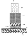
図2に、図1に示す本実施例が処理を行う被処理材の構造を模式的に示す。本図における被処理材は、ウエハ112の上面に積層され配置された膜層を有しており、本図は処理後のその膜層の一部の形状を模式的に示している。
FIG. 2 schematically shows the structure of a material to be processed which is processed by the present embodiment shown in FIG. The material to be processed in this figure has a film layer disposed on the upper surface of the
本図の膜層は、複数の膜から構成され、下地であるウエハ112のシリコン205の上面に例として4つの層からなっている。これらはレジスト(PR)又はハードマスク(SiO2,SiNまたはSiONなど)等のマスク201、その下方のPoly−Si(ポリシリコン)膜202、金属の物質から構成された材料を含む膜(例えばTiN、以下メタル膜)203、High−k(例えばHfO2)膜204の積層構造を有している。
The film layer of this figure is composed of a plurality of films, and is composed of, for example, four layers on the upper surface of the
このような膜層の構造は、半導体デバイスのゲート構造を形成するためのものであって、エッチング処理の前に所定の処理によって成膜,リソグラフィー処理によりマスク201の不要部分の除去が行われている。本図のこれらの各膜は、単一の層から構成されているが、複数の層から構成されていてもよく、特にメタル膜203は上下に各々が異なる材料からなる複数の層から構成されていても良い。また、メタル膜203の材料の種類および積層数、厚みは製造される半導体デバイスの仕様に応じNMOS部分,PMOS部分によって異なる。
Such a film layer structure is for forming a gate structure of a semiconductor device, and an unnecessary part of the
それぞれの積層膜はそれぞれ条件、ガスの組成,供給量,圧力,処理時間等の少なくとも1部が異なる所定のエッチングレシピにより処理される。またマスク201は、近年の微細加工に対応したPRだけでは、膜厚,エッチング耐性が不十分であることから、PRの下層にアモルファスカーボン(ACL)や、SiNまたはSiONおよびSiO2のハードマスクを配置して、それらをマスクに更に下層のPoly−Si膜202やメタル膜203をエッチングしてもよい。ここではマスク201のエッチング工程についての説明は省略する。
Each laminated film is processed by a predetermined etching recipe in which at least a part of conditions, gas composition, supply amount, pressure, processing time, and the like are different. Further, since the
Poly−Si膜202のエッチングの処理用ガスとしては、Cl2とフッ素(F)(例えばCF4)の混合ガス又はCl2とHBrの混合ガス等が用いられる。また必要に応じてO2等のガスも用いられる。
As a processing gas for etching the Poly-
次にメタル膜203(例えばTiN)の層のエッチング工程では、最初にメタル膜203の層の界面(上下の膜層の間でこれらの材料としての表面同士の間に形成された面であり、単一または数原子層程度の別の部材の膜が存在する場合を含めた境界部分)に形成された自然酸化膜等を除去するため、相対的に高いウエハバイアスの値にしてイオンエネルギーを増加させる。処理用のガスとしてはHBrやAr等が用いられるが、他のガス系であっても良い。 Next, in the etching process of the layer of the metal film 203 (for example, TiN), first, the interface of the layer of the metal film 203 (the surface formed between the surfaces as these materials between the upper and lower film layers, In order to remove the natural oxide film etc. formed on the boundary part including the case where a film of another member of single or several atomic layers exists, the ion energy is increased with a relatively high wafer bias value. Let As the processing gas, HBr, Ar, or the like is used, but other gas systems may be used.
この自然酸化膜除去の工程の後、メタル膜203のエッチングの為に、処理用ガスとして主にCl2またはCl2とHBrの混合ガスが用いられる。本実施例で用いられるメタル膜203のエッチングは、メタル203の層が相対的に他の膜の層より薄膜であるため、比較的低いイオンエネルギーとなるように高周波電源114からの電力によるウエハバイアスの値が調整される。
After this natural oxide film removal step, Cl 2 or a mixed gas of Cl 2 and HBr is mainly used as a processing gas for etching the
次に、高誘電率材料であるHigh−K(例えばHfO2)膜のエッチングにはBCl3又はBCl3とCl2の混合ガスが用いられる。本ステップでは相対的に低いイオンエネルギー条件を使用することにより、良好なエッチング特性(形状,選択比)等が達成される。 Next, BCl 3 or a mixed gas of BCl 3 and Cl 2 is used for etching a High-K (for example, HfO 2 ) film that is a high dielectric constant material. In this step, good etching characteristics (shape, selection ratio) and the like are achieved by using relatively low ion energy conditions.
従来は、エッチング処理したウエハの枚数が所定の枚数になると、処理室104内部のウェットクリーニング等のクリーニングを実施した後、処理室104内部を馴染ませるため、Si,PR又は酸化膜ウエハ等の非メタル系ウエハを用いたエッチングを実施して処理室104内部の部材表面のシーズニング処理を実施した後に製品用のウエハの処理を実施していた。図3は、従来の技術によりメタル/High−k積層構造の被処理材が表面に配置されたウエハを複数枚処理した際の、ウェット処理後のPoly−Siのエッチングレートの測定の結果を示すグラフである。 Conventionally, when the number of etched wafers reaches a predetermined number, after cleaning such as wet cleaning inside the processing chamber 104 is performed, the inside of the processing chamber 104 is acclimatized. After performing etching using a metal-based wafer and seasoning the surface of the member inside the processing chamber 104, the wafer for the product is processed. FIG. 3 shows the results of measurement of the etching rate of Poly-Si after wet processing when a plurality of wafers having a metal / High-k stacked structure processed material disposed thereon are processed by the conventional technique. It is a graph.
本従来技術では、複数枚のウエハの処理の枚数が増大するに伴ってエッチングレートが変化している。特に、処理開始から極初期にエッチングレートが急激に増加し、その後安定となっている。このため、クリーニングしてエッチング処理を開始した直後の製品用のウエハでの処理結果とその後所定の枚数を経て安定した結果が得られたウエハのその処理結果との間で形状に著しい差異が生じていた。 In this prior art, the etching rate changes as the number of wafers processed increases. In particular, the etching rate increases abruptly at the very beginning from the start of processing, and then becomes stable. For this reason, there is a significant difference in shape between the processing result of the product wafer immediately after cleaning and starting the etching process and the processing result of the wafer that has obtained a stable result after a predetermined number of wafers. It was.
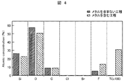
発明者らは、この原因を明らかにするため、処理室内部に処理室内壁と同種部材のテストサンプルを設置し、メタル膜203を含む膜層と含まない膜層を処理した場合の、それぞれのサンプル表面をXPS(X-ray photo-electron spectroscopy)を用いて測定した。その結果のグラフを図4として示す。この図に示すように、メタル膜203を有する膜層を処理したサンプルからはTiが検出された。更に、メタル203を含む膜層を処理したサンプルからは、フッ素(F)の増加が検出された。
In order to clarify this cause, the inventors installed a test sample of the same kind as the processing chamber wall in the processing chamber, and processed each of the film layer including the
図5は、メタル膜203とHigh−k膜204とのエッチング処理の時間をパラメータとして複数枚(本例では10枚程度)連続してエッチング処理を行って後別のウエハ112の図2に示す膜層のPoly−Si膜202のエッチング処理のレートを測定した結果を示すグラフである。図中点線は、ウエハ112を長期間処理した際の安定するPoly−Si膜202のエッチングレートである。
FIG. 5 shows another
本図に示すようにHigh−k膜204のエッチング処理の時間が少ないほどエッチングレートが高く、多いと減少する。また、ある一定以上のHigh−k膜204のエッチング処理の時間ではエッチングレートが飽和している。本実施例は、メタル膜203の材料としてTiNエッチングしたものであり、HBr/Cl2を含む処理用ガスを使用した。さらに、High−k膜204のエッチングとしてBCl3/Cl2を含む処理用ガスを使用した。また、この膜層を処理した後、Siウエハを電極上に設置し、Ar放電に暴し、その後Siウエハ表面をTRXF(Total reflection X-ray Fluorescence)により測定したものである。それぞれ検出されたTi量を右軸に示す。
As shown in this figure, the etching rate increases as the time for etching the high-
本例において、検出された金属の物質であるTiは処理室104内に粒子として残留したTiが、処理中にArのスパッタリングにより飛散し、ウエハ112上に堆積したものに起因すると考えられ、すなわち、処理室104内に残留したTiの量を示していると考えられる。従って、Poly−Si膜202のエッチング処理のレートと処理室104内に残留するTi量の間には相関があると考えられる。
In this example, Ti, which is a detected metal substance, is considered to be caused by Ti remaining as particles in the processing chamber 104 being scattered by Ar sputtering during processing and deposited on the
さらに、図4にも示したように、Tiが処理室104内に残留することによりFも同時に増加している。この原因を調べるため、XPSの測定結果を詳細に見ると(図示省略)、Ti2pピークにはTi−Oの結合の他にTi−Fのピークが観測されること、またF1sのピークには低束縛エネルギー方向へのエネルギーシフトが見られることから、Fが何らかの金属と結合していると考えられ、この場合Ti−Fの結合を有していると発明者らは考えた。このことは、処理室104内に残留するTiにより処理室104の内壁表面を構成する材料の物質がフッ化され、更にはプラズマ中のFが増加することによりPoly−Si膜の処理のレートが増加していることについても説明が可能となる。 Further, as shown in FIG. 4, F also increases at the same time as Ti remains in the processing chamber 104. In order to investigate this cause, when the XPS measurement results are viewed in detail (not shown), a Ti—F peak is observed in addition to a Ti—O bond in the Ti 2p peak, and a low in the F 1s peak. Since an energy shift toward the binding energy direction is observed, it is considered that F is bonded to some metal, and in this case, the inventors considered that it has a Ti—F bond. This is because the material of the material constituting the inner wall surface of the processing chamber 104 is fluorinated by Ti remaining in the processing chamber 104, and further, the rate of processing of the Poly-Si film is increased by increasing F in the plasma. It is possible to explain the increase.
一方、一般にTi−F,Ti−Oの結合は安定であり従来の技術によるプラズマを用いたクリーニングでは除去することが難しいと考えられる。そこで、本実施例では、製品用のウエハ112の被処理材の処理前に、予め、この被処理材に含まれるメタル(例えばTiN)膜203の材料と同じ物質を表面に有するウエハを処理して、同じ金属(メタル)の物質(例えばTi)を処理室104内部に付着させるシーズニングを行っている。このことにより、処理室104内部の処理中のガスの組成を安定化することができる。本実施例のこのような事前のクリーニングは、処理室104内部の部材の表面をウエットクリーニングした後、製品用のウエハ112を処理する前に行われる。
On the other hand, it is generally considered that Ti—F and Ti—O bonds are stable and difficult to remove by cleaning using plasma according to the conventional technique. Therefore, in this embodiment, before processing the processing material of the
本実施例のシーズニングは、複数枚のTiNを表面に配置したウエハ112を用いても良い。つまり、繰り返して事前のシーズニングを行っても良い。この際、各々異なる膜層を有する複数枚のウエハを連続して処理しても良い。処理室104内部に残留するメタル物質(Ti)の量は、シーズニングに用いるウエハ112上又はウエハ112なしの状態にて、プラズマを生成し、そのプラズマの発光を用いて検出することが可能である。図6を用いて、このメタル物質の検出について説明する。
In the seasoning of this embodiment, a
図6は、図1に示す実施例においてBCl3を含む処理用ガスを用いてプラズマを生成した場合のTiに起因する発光強度の時間変化を示すグラフである。本実施例では、この発光強度を発光データ処理装置124を用いて解析する。特に、その内部に配置された演算装置が同様に内部に配置された記憶装置内に格納された上記メタル物質を表面に配置したウエハ112をエッチング処理する間に検出した発光データを読み出して、所定のメタル物質に対応する波長の発光のデータを積分する処理を含む特定の演算を行って処理室104内に残留するTiの量を示す結果を算出し信号として出力することでTiの量が検出される。
FIG. 6 is a graph showing temporal changes in emission intensity caused by Ti when plasma is generated using a processing gas containing BCl 3 in the embodiment shown in FIG. In this embodiment, the emission intensity is analyzed using the emission
上記のように、このようなウエハ112の処理によって処理室104内部の表面に堆積する、あるいは処理室104内部に残留するTiの量が大きくなるに伴って、この後に行われる被処理材を有するウエハ112のエッチング処理のレートは変化するのであるが、Tiの量が特定の値を越えると処理のレートが所定値に漸近する、飽和状態となる。このような飽和状態になるTiの量は、飽和状態となるだけ長い時間に渡りメタル物質を含む膜を表面にウエハ112の該膜のエッチング処理を行った場合の処理室104内からの発光のデータを予め取得して解析しておいて、ウエットクリーニングを行った直後に行うメタル物質(Ti)を有する膜を表面に配置されたウエハの事前のエッチング処理を行った差異の発光強度と比較して、上記レートが飽和状態となるまでのシーズニングの終点を検出する。また、本実施例ではBCl3を含むガス系を使用したが、Ar等希ガスを用いたガス系でも同様の測定が可能である。
As described above, as the amount of Ti deposited on the surface inside the processing chamber 104 or remaining in the processing chamber 104 is increased by the processing of the
図7は、図1に示す実施例において、製品用のウエハ112表面の被処理材の処理前に上記シーズニング処理を行わなかった場合及びTiNのエッチングステップのみの処理を行った場合、TiN膜とHigh−k材料による膜の上記シーズニング処理を行い且つプラズマ発光によりシーズニングの終点判定を行った後にPoly−Si膜203をエッチング処理した際のエッチングレートの変化を示すグラフである。TiN膜とHigh−k材料による膜との処理を行った場合には、3例のなかで最もレートの変動が小さく安定な処理が実施されている。前述のようにHigh−kの材料を含む膜の処理は、BCl3を組成として含む処理用ガスを使用しており、このガスを用いた処理ではBCl3が処理室104内部に残留したTiを除去する特性がある。
FIG. 7 shows a case where, in the embodiment shown in FIG. 1, when the seasoning process is not performed before the processing of the material to be processed on the surface of the
このことから、処理室104内部の残留したTiの量を調節するためには、事前のシーズニングの処理においてTiN膜のエッチングの工程とHigh−k材料による膜のエッチングの工程との時間比又は放電条件をプラズマの発光を検出した結果得られる信号を基に調整することが重要である。このことにより事前のシーズニングの処理によって処理室104内部に残留、あるいは堆積させる金属の物質(Ti)の量を所望の量に調節することができる。 Therefore, in order to adjust the amount of Ti remaining in the processing chamber 104, the time ratio or discharge between the TiN film etching process and the high-k material film etching process in the prior seasoning process. It is important to adjust the conditions based on a signal obtained as a result of detecting plasma emission. As a result, the amount of the metal substance (Ti) remaining or deposited in the processing chamber 104 can be adjusted to a desired amount by a prior seasoning process.
また、処理室104内部の残留したTiの量を制御する際、このような膜層の構造を有する被処理材を備えたウエハ112をエッチングする際のメタル膜203とHigh−k膜204との処理に要する時間の比と等しいか20%以内の比にて、Tiシーズニング中のTiN膜/High−k材料から構成された膜の処理の時間比で処理を行うことで、シーズニング中に蓄積する処理室104内のTiの残留の分布も、実際の被処理材を処理する時と同等とする。このことは、事前のシーズニングの処理におけるTiN膜/High−k材料から構成された膜の構成を被処理材のものと同等にし、TiN膜/High−k材料から構成された膜の処理で処理室104内部のプラズマ中の金属の物質の発光の強度を被処理材を有する製品用のウエハ112の処理の際、特に、そのエッチングレート等の処理の条件が安定した状態となって得られるプラズマの発光強度と等しくなるように、事前のシーズニングでのウエハ112の処理を行うことによっても得られる。さらにまた、事前のシーズニングの処理においてTiN膜/High−k材料から構成された膜の各々を処理する際に用いられる処理用ガスの組成を含む処理の条件を被処理材を有するウエハ112の処理の条件と同じか実質的に同じと見倣せる程度に同等にすることによっても得られる。
Further, when the amount of Ti remaining in the processing chamber 104 is controlled, the
上記のような事前のシーズニングの処理は、2つ以上のステップから構成されていることになる。このような処理を行うことにより、処理室104内に残留するTiの量或いは分布をより高精度に調節することができ、プロセスの安定性を向上できる。 The prior seasoning process as described above is composed of two or more steps. By performing such processing, the amount or distribution of Ti remaining in the processing chamber 104 can be adjusted with higher accuracy, and the stability of the process can be improved.
以上のように、上記実施例では、メタル膜203およびHigh−k膜204の積層構造を有する被処理材の処理の実施前に、該被処理材に含まれるメタル膜203を構成する材料と同種のメタル物質を含む膜を表面に有するウエハを処理して当該膜をエッチング処理することで、更には、処理室104内の上記メタル物質が残留している量を、処理室内の発光をモニターすることにより検出する、或いは検出結果を用いて処理の条件を調節することにより、処理室104内のメタル物質の残留の量を安定化させ、処理の結果得られる形状の変動を抑制することが可能となる。ひいては、加工後のCD値の安定性を向上でき、処理の歩留りの低下、及び経時変化が少ないエッチング処理の装置または方法を提供することができる。
As described above, in the above-described embodiment, before the processing of the processing material having the laminated structure of the
また、処理室104内部のメタル物質の残留の量が安定化されるため、メタル物質を起因としたプロセスの変動が抑制され、CDの変動抑制が可能であるという効果がある。 In addition, since the amount of metal material remaining in the processing chamber 104 is stabilized, the process variation caused by the metal material is suppressed, and the CD variation can be suppressed.
上記の本実施例では、特にECRプラズマ装置についての実施例を述べたが、本発明は他のプラズマ生成装置または方法、例えば誘導結合型プラズマ(ICP),容量結合型プラズマ(CCP)を用いても同様の効果がある。 In the above-described embodiment, the embodiment of the ECR plasma apparatus has been described. However, the present invention uses other plasma generation apparatuses or methods, for example, inductively coupled plasma (ICP), capacitively coupled plasma (CCP). Has the same effect.
101 真空容器
102 シャワープレート
103 誘電体窓
104 処理室
105 ガス供給装置
106 真空排気口
107 導波管
108 空洞共振器
109 電界発生用電源
110 磁場発生コイル
111 ウエハ載置用電極
112 ウエハ
113 マッチング回路
114 高周波電源
115 フィルター
116 直流電源
117 冷媒用流路
118 温調器
119,122 ヒーター
120 ヒーター制御器
121 温度センサー
123 発光分光器
124 発光データ処理装置
DESCRIPTION OF
Claims (3)
前記金属と同種の金属を含有する第三の膜を表面に有するウエハをプラズマ処理した後に、前記ウエハのポリシリコン膜をエッチングし、
前記第三の膜を表面に有するウエハのプラズマ処理は、前記第一の膜をエッチングするガスと同じガスを用いてプラズマ処理する第一のステップと、前記第二の膜をエッチングするガスと同じガスを用いてプラズマ処理する第二のステップとを有し、前記処理室内の発光を用いて前記処理室内に堆積している金属の量を検出しながら、前記検出された金属の量の積分値が前記ポリシリコンのエッチングレートが安定する値となるまで行われ、
前記第一のステップ時間に対する前記第二のステップ時間の比は、前記第一の膜をエッチングする時間に対する前記第二の膜をエッチングする時間の比と同等または20%以内であることを特徴とするプラズマ処理方法。 A first film containing metal, is disposed below the first and the polysilicon film disposed above the membrane, the first oxide film disposed below the film or the first membrane In addition, in a plasma processing method of performing plasma etching on a wafer having a second film containing a material having a high dielectric constant with plasma formed in a processing chamber,
After plasma processing a wafer having a third film containing the same type of metal as the metal on the surface, the polysilicon film of the wafer is etched,
The plasma treatment of the wafer having the third film on the surface is the same as the first step of plasma treatment using the same gas as the gas for etching the first film and the gas for etching the second film. An integrated value of the detected amount of metal while detecting the amount of metal deposited in the processing chamber using light emission in the processing chamber. Is performed until the etching rate of the polysilicon becomes a stable value,
The ratio of the second step time for the first step time and wherein said first membrane is within equal to or 20% and the ratio of the time for etching the second film to the time of etching A plasma processing method.
前記金属と同種の金属を含有する第三の膜を表面に有するウエハをプラズマ処理した後に、前記ウエハのポリシリコン膜をエッチングし、
前記第三の膜を表面に有するウエハのプラズマ処理は、前記処理室内の発光を用いて前記処理室内に堆積している金属の量を検出しながら、前記検出された金属の量の積分値が前記ポリシリコンのエッチングレートが安定する値となるまで行われるとともに、前記第一の膜をエッチングするガスと同じガスを用いてプラズマ処理する第一のステップと、前記第二の膜をエッチングするガスと同じガスを用いてプラズマ処理する第二のステップとを有することを特徴とするプラズマ処理方法。 A first film containing metal, is disposed below the first and the polysilicon film disposed above the membrane, the first oxide film disposed below the film or the first membrane In addition, in a plasma processing method of performing plasma etching on a wafer having a second film containing a material having a high dielectric constant with plasma formed in a processing chamber,
After plasma processing a wafer having a third film containing the same type of metal as the metal on the surface, the polysilicon film of the wafer is etched,
In the plasma processing of the wafer having the third film on the surface, the integrated value of the detected amount of metal is detected while detecting the amount of metal deposited in the processing chamber using light emission in the processing chamber. with the etching rate of the polysilicon is performed until the value of stability, the a first step of plasma processing the first film by using the same gas as the gas for etching, a gas for etching the second film And a second step of performing plasma processing using the same gas.
前記第一の膜はTiNであり、前記第二の膜は、HfO2であり、前記HfO2は、BCl3ガスを用いてエッチングされることを特徴とするプラズマ処理方法。 The plasma processing method of placing serial to claim 1 or claim 2,
The plasma processing method, wherein the first film is TiN, the second film is HfO 2 , and the HfO 2 is etched using BCl 3 gas.
Priority Applications (4)
| Application Number | Priority Date | Filing Date | Title |
|---|---|---|---|
| JP2009018958A JP5377993B2 (en) | 2009-01-30 | 2009-01-30 | Plasma processing method |
| TW098105258A TWI442468B (en) | 2009-01-30 | 2009-02-19 | Plasma processing device and plasma processing method |
| US12/393,254 US8236701B2 (en) | 2009-01-30 | 2009-02-26 | Plasma processing apparatus and plasma processing method |
| US13/524,914 US20120252200A1 (en) | 2009-01-30 | 2012-06-15 | Plasma processing apparatus and plasma processing method |
Applications Claiming Priority (1)
| Application Number | Priority Date | Filing Date | Title |
|---|---|---|---|
| JP2009018958A JP5377993B2 (en) | 2009-01-30 | 2009-01-30 | Plasma processing method |
Publications (3)
| Publication Number | Publication Date |
|---|---|
| JP2010177480A JP2010177480A (en) | 2010-08-12 |
| JP2010177480A5 JP2010177480A5 (en) | 2012-03-15 |
| JP5377993B2 true JP5377993B2 (en) | 2013-12-25 |
Family
ID=42398059
Family Applications (1)
| Application Number | Title | Priority Date | Filing Date |
|---|---|---|---|
| JP2009018958A Expired - Fee Related JP5377993B2 (en) | 2009-01-30 | 2009-01-30 | Plasma processing method |
Country Status (3)
| Country | Link |
|---|---|
| US (2) | US8236701B2 (en) |
| JP (1) | JP5377993B2 (en) |
| TW (1) | TWI442468B (en) |
Families Citing this family (10)
| Publication number | Priority date | Publication date | Assignee | Title |
|---|---|---|---|---|
| JP5377993B2 (en) * | 2009-01-30 | 2013-12-25 | 株式会社日立ハイテクノロジーズ | Plasma processing method |
| JP5377587B2 (en) * | 2011-07-06 | 2013-12-25 | 東京エレクトロン株式会社 | Antenna, plasma processing apparatus, and plasma processing method |
| US20130115778A1 (en) * | 2011-11-04 | 2013-05-09 | Applied Materials, Inc. | Dry Etch Processes |
| JP5841917B2 (en) * | 2012-08-24 | 2016-01-13 | 株式会社日立ハイテクノロジーズ | Plasma processing apparatus and plasma processing method |
| JP6180799B2 (en) | 2013-06-06 | 2017-08-16 | 株式会社日立ハイテクノロジーズ | Plasma processing equipment |
| JP6224359B2 (en) * | 2013-06-20 | 2017-11-01 | 株式会社Screenホールディングス | Schedule creation method and schedule creation program for substrate processing apparatus |
| CN111430224B (en) | 2014-01-13 | 2023-07-28 | 应用材料公司 | Self-aligned double patterning with spatial atomic layer deposition |
| US9405089B2 (en) * | 2014-05-22 | 2016-08-02 | Texas Instruments Incorporated | High-temperature isotropic plasma etching process to prevent electrical shorts |
| JP6919350B2 (en) | 2017-06-09 | 2021-08-18 | 東京エレクトロン株式会社 | Substrate processing method and substrate processing equipment |
| US10636686B2 (en) | 2018-02-27 | 2020-04-28 | Lam Research Corporation | Method monitoring chamber drift |
Family Cites Families (16)
| Publication number | Priority date | Publication date | Assignee | Title |
|---|---|---|---|---|
| US6287977B1 (en) * | 1998-07-31 | 2001-09-11 | Applied Materials, Inc. | Method and apparatus for forming improved metal interconnects |
| US6139702A (en) * | 1999-03-05 | 2000-10-31 | United Microelectronics Corp. | Seasoning process for etcher |
| JP2002083974A (en) * | 2000-06-19 | 2002-03-22 | Semiconductor Energy Lab Co Ltd | Semiconductor device |
| JP2002025977A (en) * | 2000-07-06 | 2002-01-25 | Hitachi Ltd | Dry-etching method |
| US20030013314A1 (en) * | 2001-07-06 | 2003-01-16 | Chentsau Ying | Method of reducing particulates in a plasma etch chamber during a metal etch process |
| JP4444569B2 (en) | 2002-05-01 | 2010-03-31 | ポリマテック株式会社 | Key input device |
| US7094704B2 (en) * | 2002-05-09 | 2006-08-22 | Applied Materials, Inc. | Method of plasma etching of high-K dielectric materials |
| JP4365109B2 (en) * | 2003-01-29 | 2009-11-18 | 株式会社日立ハイテクノロジーズ | Plasma processing equipment |
| JP4504061B2 (en) * | 2004-03-29 | 2010-07-14 | 東京エレクトロン株式会社 | Plasma processing method |
| US7598167B2 (en) * | 2004-08-24 | 2009-10-06 | Micron Technology, Inc. | Method of forming vias in semiconductor substrates without damaging active regions thereof and resulting structures |
| KR100598051B1 (en) * | 2005-02-07 | 2006-07-10 | 삼성전자주식회사 | Method for fabricating semiconductor device |
| JP2007005381A (en) * | 2005-06-21 | 2007-01-11 | Matsushita Electric Ind Co Ltd | Method and apparatus for plasma etching |
| JP4849881B2 (en) * | 2005-12-08 | 2012-01-11 | 株式会社日立ハイテクノロジーズ | Plasma etching method |
| DE102006055038B4 (en) * | 2006-11-22 | 2012-12-27 | Siltronic Ag | An epitaxated semiconductor wafer and apparatus and method for producing an epitaxied semiconductor wafer |
| JP2009021584A (en) * | 2007-06-27 | 2009-01-29 | Applied Materials Inc | High temperature etching method of high k material gate structure |
| JP5377993B2 (en) * | 2009-01-30 | 2013-12-25 | 株式会社日立ハイテクノロジーズ | Plasma processing method |
-
2009
- 2009-01-30 JP JP2009018958A patent/JP5377993B2/en not_active Expired - Fee Related
- 2009-02-19 TW TW098105258A patent/TWI442468B/en not_active IP Right Cessation
- 2009-02-26 US US12/393,254 patent/US8236701B2/en not_active Expired - Fee Related
-
2012
- 2012-06-15 US US13/524,914 patent/US20120252200A1/en not_active Abandoned
Also Published As
| Publication number | Publication date |
|---|---|
| US8236701B2 (en) | 2012-08-07 |
| US20100197137A1 (en) | 2010-08-05 |
| TWI442468B (en) | 2014-06-21 |
| JP2010177480A (en) | 2010-08-12 |
| US20120252200A1 (en) | 2012-10-04 |
| TW201029064A (en) | 2010-08-01 |
Similar Documents
| Publication | Publication Date | Title |
|---|---|---|
| JP5377993B2 (en) | Plasma processing method | |
| JP5450187B2 (en) | Plasma processing apparatus and plasma processing method | |
| JP6630649B2 (en) | Plasma processing method | |
| US20090263919A1 (en) | Plasma oxidation processing method | |
| JP2004022747A (en) | Etching device and treatment method | |
| JP5750496B2 (en) | Plasma processing method | |
| US11251052B2 (en) | Plasma processing method and plasma processing apparatus | |
| JP5853087B2 (en) | Plasma processing method | |
| JP2016031955A (en) | Plasma processing apparatus and plasma processing method | |
| JP2013222910A (en) | Plasma processing method and plasma processing device | |
| JP6169666B2 (en) | Plasma processing method | |
| JP2002118095A (en) | Apparatus for manufacturing semiconductor, method for treating surface of substrate to be treated and method for observing adherence state of plasma product | |
| US6506687B1 (en) | Dry etching device and method of producing semiconductor devices | |
| US20150041060A1 (en) | Plasma processing apparatus | |
| KR101066972B1 (en) | Plasma processing apparatus and plasma processing method | |
| JP2015088696A (en) | Plasma processing method | |
| JP3661851B2 (en) | Dry etching method and dry etching apparatus | |
| JP5448945B2 (en) | Plasma processing equipment | |
| JP2017152445A (en) | Plasma processing method, and plasma processing device | |
| JPH118224A (en) | Manufacture of semiconductor device |
Legal Events
| Date | Code | Title | Description |
|---|---|---|---|
| A521 | Written amendment |
Free format text: JAPANESE INTERMEDIATE CODE: A523 Effective date: 20120110 |
|
| A621 | Written request for application examination |
Free format text: JAPANESE INTERMEDIATE CODE: A621 Effective date: 20120110 |
|
| A521 | Written amendment |
Free format text: JAPANESE INTERMEDIATE CODE: A523 Effective date: 20120110 |
|
| A977 | Report on retrieval |
Free format text: JAPANESE INTERMEDIATE CODE: A971007 Effective date: 20120830 |
|
| A131 | Notification of reasons for refusal |
Free format text: JAPANESE INTERMEDIATE CODE: A131 Effective date: 20120904 |
|
| A521 | Written amendment |
Free format text: JAPANESE INTERMEDIATE CODE: A523 Effective date: 20121030 |
|
| A131 | Notification of reasons for refusal |
Free format text: JAPANESE INTERMEDIATE CODE: A131 Effective date: 20130709 |
|
| A521 | Written amendment |
Free format text: JAPANESE INTERMEDIATE CODE: A523 Effective date: 20130718 |
|
| TRDD | Decision of grant or rejection written | ||
| A01 | Written decision to grant a patent or to grant a registration (utility model) |
Free format text: JAPANESE INTERMEDIATE CODE: A01 Effective date: 20130827 |
|
| A61 | First payment of annual fees (during grant procedure) |
Free format text: JAPANESE INTERMEDIATE CODE: A61 Effective date: 20130925 |
|
| R150 | Certificate of patent or registration of utility model |
Free format text: JAPANESE INTERMEDIATE CODE: R150 |
|
| LAPS | Cancellation because of no payment of annual fees |